JP6676888B2 - Power converter - Google Patents
Power converter Download PDFInfo
- Publication number
- JP6676888B2 JP6676888B2 JP2015123372A JP2015123372A JP6676888B2 JP 6676888 B2 JP6676888 B2 JP 6676888B2 JP 2015123372 A JP2015123372 A JP 2015123372A JP 2015123372 A JP2015123372 A JP 2015123372A JP 6676888 B2 JP6676888 B2 JP 6676888B2
- Authority
- JP
- Japan
- Prior art keywords
- base
- switching element
- capacitance
- impedance
- wiring
- Prior art date
- Legal status (The legal status is an assumption and is not a legal conclusion. Google has not performed a legal analysis and makes no representation as to the accuracy of the status listed.)
- Expired - Fee Related
Links
- 239000000758 substrate Substances 0.000 claims description 48
- 239000003990 capacitor Substances 0.000 claims description 24
- 239000002184 metal Substances 0.000 claims description 15
- 229910052751 metal Inorganic materials 0.000 claims description 15
- 238000006243 chemical reaction Methods 0.000 claims description 7
- 238000000926 separation method Methods 0.000 claims description 4
- 230000005855 radiation Effects 0.000 description 7
- 239000000919 ceramic Substances 0.000 description 5
- 238000001816 cooling Methods 0.000 description 5
- 230000008878 coupling Effects 0.000 description 5
- 238000010168 coupling process Methods 0.000 description 5
- 238000005859 coupling reaction Methods 0.000 description 5
- 230000007423 decrease Effects 0.000 description 4
- 238000010586 diagram Methods 0.000 description 4
- 239000010949 copper Substances 0.000 description 3
- 238000000034 method Methods 0.000 description 3
- 230000010355 oscillation Effects 0.000 description 3
- 230000003071 parasitic effect Effects 0.000 description 3
- 238000004519 manufacturing process Methods 0.000 description 2
- 239000000463 material Substances 0.000 description 2
- 230000002093 peripheral effect Effects 0.000 description 2
- 239000004065 semiconductor Substances 0.000 description 2
- 229910018072 Al 2 O 3 Inorganic materials 0.000 description 1
- RYGMFSIKBFXOCR-UHFFFAOYSA-N Copper Chemical compound [Cu] RYGMFSIKBFXOCR-UHFFFAOYSA-N 0.000 description 1
- 230000002411 adverse Effects 0.000 description 1
- 230000005540 biological transmission Effects 0.000 description 1
- 238000005219 brazing Methods 0.000 description 1
- 229910052802 copper Inorganic materials 0.000 description 1
- 238000005520 cutting process Methods 0.000 description 1
- 230000000694 effects Effects 0.000 description 1
- 238000009499 grossing Methods 0.000 description 1
- 230000006698 induction Effects 0.000 description 1
- 239000011810 insulating material Substances 0.000 description 1
- 230000007257 malfunction Effects 0.000 description 1
- 230000002250 progressing effect Effects 0.000 description 1
- 230000000644 propagated effect Effects 0.000 description 1
- 230000001902 propagating effect Effects 0.000 description 1
- 238000011084 recovery Methods 0.000 description 1
- 239000011347 resin Substances 0.000 description 1
- 229920005989 resin Polymers 0.000 description 1
- 238000005476 soldering Methods 0.000 description 1
- 238000001228 spectrum Methods 0.000 description 1
- 230000001629 suppression Effects 0.000 description 1
- 238000005382 thermal cycling Methods 0.000 description 1
- 229910000859 α-Fe Inorganic materials 0.000 description 1
Images


Classifications
-
- H—ELECTRICITY
- H01—ELECTRIC ELEMENTS
- H01L—SEMICONDUCTOR DEVICES NOT COVERED BY CLASS H10
- H01L2224/00—Indexing scheme for arrangements for connecting or disconnecting semiconductor or solid-state bodies and methods related thereto as covered by H01L24/00
- H01L2224/01—Means for bonding being attached to, or being formed on, the surface to be connected, e.g. chip-to-package, die-attach, "first-level" interconnects; Manufacturing methods related thereto
- H01L2224/42—Wire connectors; Manufacturing methods related thereto
- H01L2224/47—Structure, shape, material or disposition of the wire connectors after the connecting process
- H01L2224/48—Structure, shape, material or disposition of the wire connectors after the connecting process of an individual wire connector
- H01L2224/481—Disposition
- H01L2224/48135—Connecting between different semiconductor or solid-state bodies, i.e. chip-to-chip
- H01L2224/48137—Connecting between different semiconductor or solid-state bodies, i.e. chip-to-chip the bodies being arranged next to each other, e.g. on a common substrate
Description
本発明は、電力変換装置用モジュールに係わり、特にモジュールが発する高周波ノイズ信号を低減する電力変換装置用モジュールに関するものである。 The present invention relates to a power converter module, and more particularly to a power converter module that reduces a high-frequency noise signal generated by the module.
各種産業に用いられる電力変換装置のスイッチング素子としてパワーモジュールが使用されている。このパワーモジュールは、半導体素子の動作時には高周波電圧、電流振幅ノイズを発生して周辺機器へ伝導、放射して周辺機器に対し悪影響を与える。 Power modules are used as switching elements of power conversion devices used in various industries. This power module generates high-frequency voltage and current amplitude noise during the operation of the semiconductor device, and conducts and radiates the noise to peripheral devices to adversely affect the peripheral devices.
近年、パワーモジュール内で使用されるパワー半導体素子は、ゲート制御の高速化、SiCやGaN等ワイドバンドギャップ材料からなる新デバイスの採用により、ますますスイッチング時間の短縮化、スイッチング時の電圧波形の急峻化が進んでいる。これに伴い、スイッチング時の瞬間的な電圧振動(サージ電圧)、ダイオードが発する逆回復電流、ノイズ源での発生レベルが増大している。ノイズは、インピーダンスの低いループ、特に対地容量の大きい箇所を介してグランドに漏れ、グランドラインを経由して近接する他の機器に影響を与える。 In recent years, power semiconductor devices used in power modules have been increasingly shortened in switching time and voltage waveforms during switching by adopting new devices made of wide band gap materials such as SiC and GaN. The steepening is progressing. Accordingly, instantaneous voltage oscillation (surge voltage) at the time of switching, a reverse recovery current generated by a diode, and a generation level in a noise source are increasing. The noise leaks to the ground through a loop having a low impedance, particularly, a portion having a large ground capacitance, and affects other devices adjacent to the device via the ground line.
インバータ装置等の電力変換装置からグランドに漏れるノイズ電流を低減する技術として、使用されるパワーモジュールの絶縁基板のインピーダンスを高めるために、特許文献1では誘電損失が大きくなる材料からなる絶縁基板を用いることを提案している。また、特許文献2では、パワーモジュールの絶縁基板を2層構造にし、そのうち1層には絶縁基板に対し並列にインダクタンスとして寄与する配線層等を設け、LCによる並列共振によって特定周波数でのインピーダンスを高め、グランドへの漏れ電流を軽減することを提案している。
As a technique for reducing a noise current leaking from an electric power converter such as an inverter to the ground, in order to increase the impedance of an insulating substrate of a power module to be used, Patent Document 1 uses an insulating substrate made of a material having a large dielectric loss. Propose that. In
一方、特許文献3では、インバータの出力ケーブルとグランドパターン間の容量(電気的結合)を高めることで、入力ケーブルと出力ケーブル間の電気的結合を低減し、出力ケーブルに重畳する高周波ノイズが入力ケーブル、電源側に伝達、誘導され難い構成を提案している。また、特許文献4では、主なノイズ源であるインバータのスイッチング素子とグランド電位のヒートシンク間の電気的結合を広い周波数で高めるために、コンデンサとして働く容量素子(インピーダンス回路)をヒートシンク上に作成し、高周波ノイズ電流をグランドに積極的に逃がすことで、電源側に高周波電流が流れにくくした構成を提案している。
On the other hand, in
特許文献2で提案されている技術では、パワーモジュールの絶縁基板を従来の1層の絶縁層ではなく多層基板にしているため、パワーモジュールの製造コストアップに繋がり、且つ絶縁層内に配線パターンを設けること及びチップインダクタを配置すること等、製造工程も複雑化するという問題がある。また、所望のインピーダンス特性を得るには、配線パターンの長さ、太さ、位置等に詳細な制約が生じる。また、IGBT等スイッチング素子のゲート制御条件により発生するノイズの周波数も異なり、スイッチング素子の使用条件ごとにインピーダンスを高めるべき周波数帯も変動する。すなわち、絶縁基板での回路設計を、スイッチング素子の特性、及びゲート制御、動作温度条件等の使用条件ごとに設計しなおすことが必要になる。
In the technique proposed in
特許文献3,4は、システムの大型化、コストアップに繋がるノイズ部品(フェライトコアやノイズ抑制シート、LCフィルタ)の使用を最小限にするため、システム内の各部位間の電気的,磁気的結合を制御することで、ノイズの伝搬ルートを制御するものである。各制御方法では、以下のような問題が生じる。
特許文献3においては、出力ケーブルとグランド間の容量は、U相,V相,W相の出力電線とグランド電位パターン間の絶縁部材の厚み、ケーブル内の対向表面積(最接近で向かい合った部位の表面積)等で決まるが、比誘電率が3程度以下の通常の絶縁材料を用いた場合、両者間の結合容量は大きくても100pF以下であり、10MHz以下の周波数のノイズ成分を逃がす伝搬ルートとしては十分に低いインピーダンスにはならない。
In
特許文献4においては、スイッチング素子前後の各主回路電位(P電位,N電位,U相,V相,W相)とグランド間の容量は各電位で異なるため、各電位からグランドへ漏れるルート間でインピーダンス特性(インピーダンスが低下する共振周波数)が異なる。すなわち、広い周波数帯において全電位からグランドまでのインピーダンスを低下させるには、各電位と容量のバラツキを考慮した上で、最適な定数を持つ複数の容量素子を設けなければならない。また、ノイズの伝搬ルートを制御するという観点とは別に、スイッチング時の放射ノイズを抑制するという観点からは、高周波電流が循環するループをできるだけ狭い領域に制限する必要がある。 In Patent Literature 4, since the capacitance between each main circuit potential (P potential, N potential, U phase, V phase, W phase) before and after the switching element and the ground is different at each potential, between the routes leaking from each potential to the ground. Characteristic differs (resonance frequency at which the impedance decreases). That is, in order to reduce the impedance from the entire potential to the ground in a wide frequency band, it is necessary to provide a plurality of capacitance elements having optimal constants in consideration of variations in each potential and capacitance. In addition to controlling the noise propagation route, from the viewpoint of suppressing radiation noise at the time of switching, it is necessary to limit the loop in which the high-frequency current circulates to a region as narrow as possible.
本発明が目的とするところは、高周波ノイズ電流を、ノイズ発生源近傍に閉じ込めることでモジュール外部へ伝導するノイズ、放射するノイズを低減した電力変換装置用モジュールを提供することにある。 An object of the present invention is to provide a module for a power converter in which a high-frequency noise current is confined in the vicinity of a noise generation source to reduce noise conducted and radiated outside the module.
本発明は、
コンデンサと、
前記コンデンサの一端に接続され、直流電圧の正電位が印加される正極電位端と、前記コンデンサの他端に接続され、直流電圧の負電位が印加される負極電位端と、前記正極電位端と負極電位端の間に、配線を介して直列に接続された第1、第2のスイッチング素子と、前記第1のスイッチング素子に配線を介して逆並列接続された第1のダイオードと、前記第2のスイッチング素子に配線を介して逆並列接続された第2のダイオードと、から成る回路を有したモジュールと、
を備えた電力変換装置であって、
前記モジュールは、
第1の絶縁基板の一方の面に前記正極電位端を配設し、第1の絶縁基板の他方の面に金属よりなる第1のベースを配設し、
第2の絶縁基板の一方の面に、前記第1および第2のスイッチング素子の共通接続点と、第1および第2のダイオードの共通接続点で形成される交流出力端を配設し、第2の絶縁基板の他方の面に金属よりなる第2のベースを配設し、
第3の絶縁基板の一方の面に前記負極電位端を配設し、第3の絶縁基板の他方の面に金属よりなる第3のベースを配設し、
前記第1のベースと第2のベースの間に第1のインピーダンス調節用の部材を介挿し、
前記第2のベースと第3のベースの間に第2のインピーダンス調節用の部材を介挿したことを特徴としたものである。
The present invention
A capacitor,
Is connected to one end of the capacitor, and the positive electrode potential end positive potential is applied DC voltage is connected to the other end of the capacitor, the negative electrode potential ends negative potential of the DC voltage is applied, and the positive electrode potential end A first switching element connected in series via a wiring between negative electrode potential terminals, a first diode connected in anti-parallel to the first switching element via a wiring, A second diode connected in anti-parallel to the second switching element via wiring , and a module having a circuit consisting of:
A power converter comprising:
The module comprises:
The positive electrode potential end is disposed on one surface of a first insulating substrate, and a first base made of metal is disposed on the other surface of the first insulating substrate;
An AC output terminal formed on one surface of the second insulating substrate and formed by a common connection point of the first and second switching elements and a common connection point of the first and second diodes; A second base made of metal is provided on the other surface of the second insulating substrate,
Disposing the negative potential end on one surface of a third insulating substrate, disposing a third base made of metal on the other surface of the third insulating substrate,
Inserting a first impedance adjusting member between the first base and the second base;
A second impedance adjusting member is interposed between the second base and the third base.
本発明における第1および第2のインピーダンス調節用の部材は、
前記直列接続された第1および第2のスイッチング素子のうち、オフ制御された側のスイッチング素子のコレクタ−エミッタ間又はドレイン−ソース間の接合容量と、前記オフ制御されたスイッチング素子および該スイッチング素子に逆並列接続されたダイオードの配線と、前記配線および第3のベース間の容量又は前記配線および第1のベース間の容量と、前記第2のインピーダンス調節用の部材又は第1のインピーダンス調節用の部材と、前記第2のベースおよび交流出力端間の容量とを介して流れるノイズ電流が伝搬するループのLC直列共振周波数が10MHz以下になるように、各々インピーダンスが調節されていることを特徴としたものである。
The first and second impedance adjusting members according to the present invention include:
Of the first and second switching elements connected in series, a junction capacitance between a collector and an emitter or a drain and a source of the switching element on the off-controlled side, the off-controlled switching element, and the switching element And a capacitance between the wiring and the third base or a capacitance between the wiring and the first base and the second impedance adjusting member or the first impedance adjusting. features of the member, such that the second base and the LC series resonant frequency of the loop, the noise current is propagated flowing through the capacitance between the AC output terminals is below 10 MHz, that each impedance is adjusted It is what it was.
本発明における第1のインピーダンス調節用の部材は、0.1〜10μHの第1のインダクタンスとして機能する部材であり、前記第2のインピーダンス調節用の部材は、0.1〜10μHの第2のインダクタンスとして機能する部材であることを特徴としたものである。 The first impedance adjustment member according to the present invention is a member that functions as a first inductance of 0.1 to 10 μH , and the second impedance adjustment member is a second inductance of 0.1 to 10 μH. It is a member that functions as an inductance .
本発明における第1および第2のインダクタンスとして機能する部材は、各々チップインダクタであることを特徴としたものである。 In the present invention , each of the members functioning as the first and second inductances is a chip inductor .
本発明における第1および第2のインダクタンスとして機能する部材は、各々極細の線をコイル状に巻いたばね形状であることを特徴としたものである。 The member functioning as the first and second inductances according to the present invention is characterized in that each member has a spring shape in which an extremely fine wire is wound in a coil shape .
本発明は、前記第1および第2のインダクタンスとして機能する部材のインダクタンス値は、前記コンデンサの容量と、正極電位端および負極電位端と第1および第2のスイッチング素子を結ぶ配線と、第1および第2のスイッチング素子のうち、オフ制御されたスイッチング素子のコレクタ−エミッタ間又はドレイン−ソース間の接合容量とを介して流れるノイズ電流が伝搬するループのLC直列共振周波数よりも、
前記直列接続された第1および第2のスイッチング素子のうち、オフ制御された側のスイッチング素子のコレクタ−エミッタ間又はドレイン−ソース間の接合容量と、前記オフ制御されたスイッチング素子および該スイッチング素子に逆並列接続されたダイオードの配線と、前記配線および第3のベース間の容量又は前記配線および第1のベース間の容量と、前記第2のインピーダンス調節用の部材又は第1のインピーダンス調節用の部材と、前記第2のベースおよび交流出力端間の容量とを介して流れるノイズ電流が伝搬するループのLC直列共振周波数が小さくなるように各々選定されていることを特徴としたものである。
According to the present invention , the inductance value of the member functioning as the first and second inductances may be a capacitance of the capacitor, a wiring connecting a positive potential terminal and a negative potential terminal to the first and second switching elements, And the second series switching element, than the LC series resonance frequency of the loop in which the noise current flowing through the collector-emitter or drain-source junction capacitance of the off-controlled switching element propagates
Of the first and second switching elements connected in series, a junction capacitance between a collector and an emitter or a drain and a source of the switching element on the off-controlled side, the off-controlled switching element, and the switching element And a capacitance between the wiring and the third base or a capacitance between the wiring and the first base and the second impedance adjusting member or the first impedance adjusting. is obtained is characterized in that a member of, said second base and loops of the LC series resonance frequency of the noise current propagates flowing through the capacitance between the AC output terminals are respectively selected to be smaller .
本発明は、コンデンサとモジュールを備えた電力変換装置であって、
前記モジュールは、
前記コンデンサの一端に接続され、直流電圧の正電位が印加される正極電位端と、前記コンデンサの他端に接続され、直流電圧の負電位が印加される負極電位端と、前記正極電位端と負極電位端の間に、配線を介して直列に接続された第1、第2のスイッチング素子と、前記第1のスイッチング素子に配線を介して逆並列接続された第1のダイオードと、前記第2のスイッチング素子に配線を介して逆並列接続された第2のダイオードと、を備え、
金属よりなる第1のベースと、第1のベースに積層された第1の絶縁基板と、第1の絶縁基板に積層され、前記正極電位端と接続された正極配線層と、正極配線層に各々個別に積層された第1のスイッチング素子および第1のダイオードと、第1のスイッチング素子および第1のダイオードに積層された、第1および第2のスイッチング素子の共通接続点と第1および第2のダイオードの共通接続点で形成される交流出力部と、交流出力部に各々個別に積層された第2のスイッチング素子および第2のダイオードと、第2のスイッチング素子および第2のダイオードに積層され、前記負極電位端と接続された負極配線層と、負極配線層に積層された第2の絶縁基板と、第2の絶縁基板に積層された金属よりなる第2のベースとを、絶縁性の筐体内に、前記第1および第2のベースを挟んだ状態で収納し、
一端が、前記絶縁性の筐体における前記第1のベースと第2のベースの中間位置に相当する部位に貫通された交流出力部を、前記筐体内の第1のベースと第2のベースの間に収納し、
前記第1のベースにおける、前記正極配線層および第1のベース間の容量が形成される部位と、前記交流出力部および第1のベース間の容量が形成される部位の近接箇所を分離し、該分離箇所に第1のインピーダンス調節用の部材を介挿し、
前記第2のベースにおける、前記負極配線層および第2のベース間の容量が形成される部位と、前記交流出力部および第2のベース間の容量が形成される部位の近接箇所を分離し、該分離箇所に第2のインピーダンス調節用の部材を介挿したことを特徴としたものである。
The present invention is a power conversion device including a capacitor and a module,
The module comprises:
A positive potential terminal connected to one end of the capacitor, to which a positive potential of a DC voltage is applied; a negative potential terminal connected to the other end of the capacitor, to which a negative potential of a DC voltage is applied; A first switching element connected in series via a wiring between negative electrode potential terminals, a first diode connected in anti-parallel to the first switching element via a wiring, A second diode connected in anti-parallel to the second switching element via wiring.
A first base made of metal, a first insulating substrate laminated on the first base, a positive wiring layer laminated on the first insulating substrate and connected to the positive potential terminal, A first switching element and a first diode, each of which is individually stacked; a common connection point of the first and second switching elements, which are stacked on the first switching element and the first diode; An AC output section formed at a common connection point of the two diodes, a second switching element and a second diode individually stacked on the AC output section, and an AC output section stacked on the second switching element and the second diode. The negative electrode wiring layer connected to the negative electrode potential terminal, a second insulating substrate laminated on the negative electrode wiring layer, and a second base made of metal laminated on the second insulating substrate are electrically insulated. Enclosure Within, housed in a state of sandwiching the first and second base,
An AC output part having one end penetrated at a portion corresponding to an intermediate position between the first base and the second base in the insulating casing is connected to the first base and the second base in the casing. Stored in between,
In the first base, a portion where a capacitance is formed between the positive electrode wiring layer and the first base is separated from an adjacent portion where a capacitance is formed between the AC output portion and the first base, A first impedance-adjusting member is inserted into the separation point,
In the second base, a portion where a capacitance is formed between the negative electrode wiring layer and the second base is separated from an adjacent portion where a capacitance is formed between the AC output portion and the second base, It is characterized in that a second impedance adjusting member is interposed at the separation point.
本発明は、前記第1又は第2のインダクタンスとして機能する部材のうち、少なくとも何れか一方の部材の、サイズ、数量及び第1、第2の絶縁基板と対向する位置の何れかにより、前記第1又は第2のベースの少なくとも何れか一方の面積を調節して、前記正極配線層および第1のベース間の容量、前記負極配線層および第2のベース間の容量の少なくとも何れか一方を可変することを特徴としたものである。 According to the present invention , at least one of the members functioning as the first or second inductance has a size, a quantity, and a position facing the first and second insulating substrates. The area of at least one of the first and second bases is adjusted to change at least one of the capacity between the positive wiring layer and the first base and the capacity between the negative wiring layer and the second base. It is characterized by doing .
以上のとおり、本発明によれば、以下のような効果が得られるものである。
(1)電力変換装置内のスイッチング素子の電圧変動が原因で生ずる高周波ノイズ電流を低周波から高周波にわたり、ノイズ源近傍のモジュール内で周波数毎に分離して閉じ込める複数のループができるため、EMC(電磁両立性)性能が向上し、モジュールの外部に伝導するノイズ、放射ノイズが低減する。
(2)スイッチング中に、高周波電流が複数の低インピーダンスループを同時に流れることがなくなるため、スイッチング中の任意のタイミングにおいて瞬間的に伝導ノイズ、放射ノイズが増大することが低減する。これにより、スイッチング中でのスイッチング素子の誤動作が防止される。
(3)モジュールの信頼性が向上する。モジュールのベースを電位毎に分離するため、例えば活性金属ろう付け法や銅直接接合法等で作成したセラミックス基板の表面側(回路パターン側)と裏面側(ベース側)の金属の面積比が近くなるため、セラミックス基板・金属の界面にかかる応力が低減され、セラミックス基板の熱サイクルに対する信頼性が向上する。また、セラミックス間に設置するインダクタや極細のばねはセラミックス基板間の応力を緩和する役目をする。
As described above, according to the present invention, the following effects can be obtained.
(1) Since a plurality of loops for separating and confining a high-frequency noise current generated by a voltage fluctuation of a switching element in a power conversion device from a low frequency to a high frequency in a module near a noise source for each frequency are formed. Electromagnetic compatibility) performance is improved, and noise and radiation noise transmitted to the outside of the module are reduced.
(2) During switching, a high-frequency current does not flow through a plurality of low-impedance loops at the same time, so that instantaneous increase in conduction noise and radiation noise at any timing during switching is reduced. This prevents a malfunction of the switching element during switching.
(3) Module reliability is improved. Since the base of the module is separated for each potential, the area ratio of the metal on the front side (circuit pattern side) and the back side (base side) of the ceramic substrate made by, for example, active metal brazing or copper direct bonding is close. Therefore, the stress applied to the interface between the ceramic substrate and the metal is reduced, and the reliability of the ceramic substrate with respect to thermal cycling is improved. Inductors and extra-fine springs placed between the ceramics serve to relieve the stress between the ceramic substrates.
本発明は、電力変換装置に使用されるモジュールのP(正極)電位、N(負極)電位およびAC(交流)電位の電極パターンと絶縁基板を介して主要な容量を形成する金属部(ベース)を、対向する電位毎に分離し、P電位と対向するベースとAC電位と対向するベースとの間、N電位と対向するベースとAC電位と対向するベースとの間にそれぞれ0.1μH〜10μHのインダクタンスとして寄与する部材を介挿するものである。具体的な実施例の説明に先立って、本発明に至る考え方について説明する。 The present invention relates to a metal part (base) that forms a main capacitance through an electrode pattern of a P (positive electrode) potential, an N (negative electrode) potential, and an AC (alternating current) potential of a module used in a power conversion device and an insulating substrate. Are separated for each of the opposing potentials, and between the base opposing the P potential and the base opposing the AC potential, and between the base opposing the N potential and the base opposing the AC potential, respectively. Is inserted with a member that contributes as an inductance. Prior to the description of the specific embodiments, the concept leading to the present invention will be described.
図7は電力変換装置の例として一般的なインバータ装置の構成を示したものである。コンバータ3は入力配線部2を介し商用電源1に接続されて交流入力電圧を直流電圧に変換する。変換された直流電圧は平滑コンデンサやスナバコンデンサを有する直流(DC)配線部4を通してインバータ5に印加され、このインバータ5において所定の交流電圧に逆変換されて出力配線部6を介して誘導機7に印加される。
FIG. 7 shows a configuration of a general inverter device as an example of a power conversion device. The
インバータ5として、IGBTやMOSFETのスイッチング素子とダイオードをモジュール化したものが使用され、スイッチング中の電圧変化dv/dtが大きいほど、またスイッチング時の電圧の跳ね上がり、電圧のリンギングが大きいほど発するノイズレベルは増大する。すなわち、高速にスイッチングすればするほどスイッチング損失は減少し変換効率向上が図れるが、ノイズレベルは増大するという問題がある。
As the
図8は、図7で示すインバータ装置の各部の浮遊容量の等価回路を示したもので、矢印で示す方向に漏れ電流が流れ、各構成部品の対地容量を介したグランドへの漏れ電流が主なノイズ伝搬ルートになる。伝導ノイズの規格を満たすためには、ノイズ源(図8では例としてW相のみを表示)のノイズ発生量の絶対値を低減すると同時に、入力配線部側、商用電源側にノイズが回り込まないよう高周波電流が伝搬する経路のインピーダンスの制御が重要となる。特に商用電源側に高周波のノイズ信号が伝搬されないように、また、空間にノイズが放射されないようにするためには、ノイズ源のできるだけ近傍で、意図的に低いインピーダンスの伝導ループを作成し、高周波の電流を狭い流域に閉じ込めることが有用である。 FIG. 8 shows an equivalent circuit of the stray capacitance of each part of the inverter device shown in FIG. 7, in which a leakage current flows in a direction shown by an arrow, and a leakage current to the ground via a ground capacitance of each component is mainly. It becomes a noise propagation route. In order to satisfy the specification of the conducted noise, the absolute value of the noise generation amount of the noise source (only the W phase is shown in FIG. 8 as an example) is reduced, and at the same time, the noise is prevented from entering the input wiring section side and the commercial power supply side. It is important to control the impedance of the path through which the high-frequency current propagates. In particular, to prevent high-frequency noise signals from propagating to the commercial power supply and to prevent noise from being radiated into the space, intentionally create a conduction loop with low impedance as close to the noise source as possible, It is useful to confine this current to a narrow watershed.
図9は一般的なインバータの2in1モジュールの断面図、図10は両面冷却型2in1モジュールの断面図を示したものである。モジュールは、Al2O3などの絶縁基板10を介して一方の面にはCuなどよりなるベース11を配置し、他方の面にはCuなどよりなる配線層12、スイッチング素子(IGBT又はMOSFET)13およびダイオード14が配設されている。15は例えばAlなどの配線である。
FIG. 9 is a cross-sectional view of a 2in1 module of a general inverter, and FIG. 10 is a cross-sectional view of a double-sided cooling 2in1 module. In the module, a
図11はこれら2in1モジュールの等価回路を示したもので、例としてインバータの下アームスイッチング素子のターンオフ時をノイズ発生源とし、そのときの伝搬ルートを示したものである。何れも、モジュールの絶縁基板10を介してP電位、N電位、AC電位と、グランド電位に落とされることの多いベース11の間に容量CP-G,CN-G,CAC-Gが形成される。
FIG. 11 shows an equivalent circuit of these 2in1 modules, and shows a propagation route at the time of turning off the lower arm switching element of the inverter as a noise source as an example. In any case, capacitors C PG , C NG , and C AC-G are formed between the P potential, the N potential, and the AC potential and the base 11 that is often dropped to the ground potential via the insulating
また、スイッチング素子としてIGBTを用いた場合、コレクタ−エミッタ間の接合容量Cce(MOSFETの場合にはドレイン−ソース間の接合容量Cds)と、直流配線部4のスナバコンデンサ(フィルムコンデンサ)の容量Cfilmとし、スナバコンデンサを含む循環ループ(以下、この循環ループをノイズ伝搬ルート1という)の寄生インダクタンスをL、寄生抵抗をRとすると、(1)式で示される周波数fでLC直列共振が発生し、その周波数でインピーダンスが寄生抵抗Rに低下する。このため、ノイズ伝搬ルート1で示されるループでは、ノイズ源が発生するノイズスペクトルのうち、共振周波数f前後の高周波振動電流が優先的に流れる。 When an IGBT is used as the switching element, the junction capacitance Cce between the collector and the emitter (drain-source junction capacitance Cds in the case of a MOSFET) and the capacitance Cfilm of the snubber capacitor (film capacitor) of the DC wiring section 4 are used. Assuming that a parasitic inductance of a circulating loop including a snubber capacitor (hereinafter, this circulating loop is referred to as a noise propagation route 1) is L and a parasitic resistance is R, LC series resonance occurs at a frequency f represented by the equation (1). At that frequency, the impedance drops to the parasitic resistance R. For this reason, in the loop indicated by the noise propagation route 1, a high-frequency oscillation current around the resonance frequency f flows preferentially in the noise spectrum generated by the noise source.

ノイズ伝搬ルート1とは別の高周波ノイズ電流のループとして、コレクタ−エミッタ間の接合容量Cce、N電位、N電位とベース間の容量CNG、AC電位とベース間の容量CAC-G、AC電位を介してベースを循環するノイズ伝搬ルート2と、スイッチング素子と逆並列に配置されるダイオードの容量CAK、AC電位、コレクタ−エミッタ間の接合容量Cce、配線15を循環するノイズ伝搬ルート3が存在する。
As a loop of a high-frequency noise current different from the noise propagation route 1, a junction capacitance Cce between the collector and the emitter, an N potential, a capacitance C NG between the N potential and the base, a capacitance C AC-G between the AC potential and the base, AC A
それぞれのループを流れるノイズ電流は、LC直列共振によりインピーダンスが低下する周波数前後となるが、その共振周波数は図11に示すように、スイッチング中のIGBT(図11では下アームのIGBT)のコレクタ−エミッタ電圧Vceに依存する。これはスイッチング中のIGBTやダイオードの接合容量がコレクタ−エミッタ電圧Vce、或いはダイオードのアノード−カソード電圧が大きいほど接合容量Cceが低下することで変化するためである。 The noise current flowing through each loop is around the frequency at which the impedance is reduced by the LC series resonance, and the resonance frequency is the collector of the IGBT during switching (the IGBT of the lower arm in FIG. 11) as shown in FIG. It depends on the emitter voltage Vce. This is because the junction capacitance of the IGBT or the diode during switching changes as the collector-emitter voltage Vce or the anode-cathode voltage of the diode increases as the junction capacitance Cce decreases.
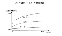
ここで問題となるのは、電圧Vceによる依存性が図12に示すように、ノイズ伝搬ルート2と3の共振周波数がある電圧Vceで非常に接近し、場合によっては一致するため、この電圧Vceではノイズ信号が両ルートに流れて伝導ノイズ、放射ノイズが大きくなる。
The problem here is that the dependence on the voltage Vce is very close to the resonance frequency of the
また、ノイズ伝搬ルート1〜3において、共振周波数が最も低いルート1の場合でも、通常10MHz以上であり、伝導ノイズの主要な成分である10MHz以下の成分を循環させるループにはなっていない。10MHz以下の低周波のノイズ信号は、図11で示すループより外部の、すなわち、図7で示す出力配線部6、直流配線部4、コンバータ3及び入力配線部2まで広がる広い領域(空間)の低インピーダンスのルートを伝搬することになる。これはインバータ装置のEMCを高めるために各種ノイズフィルタの設置、放射ノイズを抑えるための各種シールド対策が追加的に必要となり好ましくない。
よって、本発明では、ノイズ伝搬ルート1〜3等のノイズ源近傍のループのインピーダンス(共振周波数)を適切に調節設定することでノイズ信号を閉じ込めるものである。
Further, in the noise propagation routes 1 to 3, even in the case of the route 1 having the lowest resonance frequency, the frequency is usually 10 MHz or more, and does not form a loop for circulating a component of 10 MHz or less which is a main component of the conducted noise. The low-frequency noise signal of 10 MHz or less has a large area (space) outside the loop shown in FIG. 11, that is, the
Therefore, in the present invention, the noise signal is confined by appropriately adjusting and setting the impedance (resonance frequency) of the loop near the noise source such as the noise propagation routes 1 to 3.
図1は、例としてスイッチング素子をIGBTとし、U相の直列接続された上アーム用のIGBT-u1と下アーム用のIGBT-u2とを有するインバータの2in1モジュールの断面図を示したものである。各IGBTは、図9と同様に絶縁基板10を挟んで一方の面にベース11を配置し、他方の面に配線層12を介してスイッチング素子13-u1,13- u2とダイオード14-u1,14-u2を配置している。図9と異なる部分は、モジュール内におけるベース11が、IGBT-u1とIGBT-u2が直列接続されて交流を出力するAC部分と、IGBT-u2とN電位の部分で分離されている。
FIG. 1 is a cross-sectional view of a 2-in-1 module of an inverter having an IGBT as a switching element and having an upper-arm IGBT-u1 and a lower-arm IGBT-u2 connected in series in a U-phase. . In each IGBT, a
すなわち、ベース11は電位的には、対向するP電位、N電位、AC電位で分離し、その分離した位置にインピーダンス調整用の部材であるインダクタ21,22が介挿される。介挿されるインダクタ21,22は、容量数100nH〜10μH程度のインダクタンスとして機能する部材が用いられる。このインダクタとしては、例えば表面実装タイプのチップコイルとし、IGBT-u1とIGBT-u2のベース間およびIGBT-u2とN電位のベース間においてそれぞれ半田付けなどの手法で接続される。なお、インダクタ21,22としては、図2で示すようにSUS製のピアノ線をコイル状に巻いた極細のスプリングを配置してもよく、要はインダクタンス値が100nH〜10μHの範囲で作用すればよい。
That is, the
図3はインダクタ21,22を接続したときの等価回路において、IGBT-u2のターンオフ時で、IGBT-u2がノイズ源となったときのノイズ伝搬ルートを示したものである。また、図4はノイズ伝搬ルート毎の共振周波数を示したもので、インダクタンスとして動作するインダクタ21,22を配設したことで、ノイズ伝搬ルート2の共振周波数が低周波側に移動している。
FIG. 3 shows a noise propagation route when the IGBT-u2 becomes a noise source when the IGBT-u2 is turned off in an equivalent circuit when the
例えば、モジュールをIGBTで構成し、インダクタ21,22として10μH定格のチップインダクタンスを配設した場合、ノイズ伝搬ルート2の循環インダクタンスが10μH、容量CP-G=200pF,CAC-G=200pF,IGBT-u2のCce(Vce=0V時の)=20nF,IGBT-u1のCce(Vce=600V時の)=1nFの場合、ノイズ伝搬ルート2の共振周波数は、IGBTのドレイン−ソース間の接合容量Cceによらず5MHzとなる。
For example, when the module is configured by an IGBT and a chip inductance rated at 10 μH is provided as the
一方、ノイズ伝搬ルート1の共振周波数は、ルート1のループインダクタンスが30nHの場合、エミッタ−コレクタ間Vce=0Vで6.5MHz、Vce=600Vで30MHzとなる。すなわち、図4に示すようにノイズ伝搬ルート2の共振周波数は、IGBTのエミッタ−コレクタ間の接合容量Cceによらずノイズ伝搬ルート1の共振周波数に比べて低くなる。
On the other hand, when the loop inductance of the route 1 is 30 nH, the resonance frequency of the route 1 is 6.5 MHz at Vce = 0 V between the emitter and the collector, and 30 MHz at Vce = 600 V. That is, as shown in FIG. 4, the resonance frequency of the
この結果、図12で見られるような複数のノイズ伝搬ルートでの共振周波数の接近や一致による伝導ノイズ、放射ノイズの増大がなくなり、さらに周波数10MHz以下の伝導ノイズの主要成分を、ノイズ源(スイッチング素子13)近傍の循環ルート(ノイズ伝搬ルート2)に高強度で閉じ込めることができる。 As a result, conduction noise and radiation noise do not increase due to approaching or coincidence of resonance frequencies in a plurality of noise propagation routes as shown in FIG. 12, and a main component of conduction noise having a frequency of 10 MHz or less is reduced to a noise source (switching). It can be confined to the circulation route (noise propagation route 2) near the element 13) with high intensity.
なお、インダクタ21,22のインダクタンス値が大きいものを用いれば用いるほどインダクタの抵抗Rが大きくなり、共振時のインピーダンスが大きくなってノイズ電流が外部の低インピーダンスのルートを通る可能性が高まる。すなわち、インダクタ21,22のインダクタンス値は可能な限り小さな部品を用いることが望ましい。また、図1の構成とすることで、ベース11の電圧振動は図8で示す従来よりも大きくなるが、ベース11をインバータ装置のグランドに落とす方が良いか否かは系により考慮され、グランドに落とす場合は低インピーダンスを介して落とされる。
Note that the larger the
図3では、下アームのスイッチング素子のターンオフ時について説明してきたが、上アームの場合も下アームと同様に、P電位とAC電位間で形成されたインダクタンスにより、ベース電位を介するループの共振周波数を10MHz以下に低下するため、スイッチング時のノイズ閉じ込めルートが形成される。 In FIG. 3, the case where the switching element of the lower arm is turned off has been described, but also in the case of the upper arm, the resonance frequency of the loop via the base potential is determined by the inductance formed between the P potential and the AC potential, similarly to the lower arm. Is reduced to 10 MHz or less, so that a noise confinement route at the time of switching is formed.
図5は両面冷却カード型2in1モジュールに本発明を適用した場合の実施例である。両面冷却カード型2in1モジュールは、樹脂よりなるケース16によりベース11の左右一部を挟んだ状態で収納体を構成し、その内部にスイッチング素子およびダイオード等の各部品が配置されている。すなわち、P電位の配線層12Pと交流出力部(AC端子)17間にはスイッチング素子13-u1とダイオード14-u1が配置され、N電位の配線層12NとAC端子17間にはスイッチング素子13-u2とダイオード14-u2が配置されている。また、配線層12P,12Nとケース16にはそれぞれ積層された状態の絶縁基板10とベース11が配置されている。
FIG. 5 shows an embodiment in which the present invention is applied to a double-sided
上記のように構成されたモジュールにおいて、ベース11は図面左右でそれぞれに絶縁基板10と分離され、その分離された部分にそれぞれインダクタ21,22が配置されている。これにより、実施例1と同様にベース11に形成される電位部において、AC電位(AC端子17)と主要な容量CAC-Gを形成するベース電位と、P電位と主要な容量CP-Gを形成しているベース電位との間、およびN電位と主要な容量CN-Gを形成しているベース電位と、AC電位と主要な容量CAC-Gを形成するベース電位との間に、それぞれ0.1〜10μHのインダクタンスとして機能する部材を配置した構成になっている。
In the module configured as described above, the
図6は、絶縁基板10と対向配置されるベース11とインダクタ配置の他の例の平面図を示したものである。すなわち、インダクタは図面左右位置に21a(22a)を配置し、図面上下位置に21b(22b)を配置したものである。これは、絶縁基板10(或いはケース16)に接触するベース11の面積の大小で容量CP-G,CN-Gが決まることに基づく。例えば容量CP-Gは(2)式で決まる。
CP-G=絶縁基板の誘電率(ε)×S(絶縁基板に接触する面積)/絶縁基板の厚み(d)…(2)
そのため、図6で示すようにベース11をスプリング等で刻む数(図6では4箇所)を増やすか、或いは長いスプリング等で刻むことにより、絶縁基板10と対向(接触)するベース11の面積を減少させる。その結果、(2)式にしたがって容量CP-Gが減少する。図6(a)(b)ではその面積S1,S2を図6(a)>図6(b)とした例で、この大小関係でN電位とベース間容量CN-Gを例にすると、S1>S2では、CN-G1>CN-G2となる。このように、インダクタのサイズ、数量及び絶縁基板に10に対向する位置により、容量CP-G,CN-Gを可変することができる。
FIG. 6 is a plan view of another example of the arrangement of the
C PG = dielectric constant of insulating substrate (ε) × S (area in contact with insulating substrate) / thickness of insulating substrate (d) (2)
Therefore, as shown in FIG. 6, the number of
したがって、実施例2においても、実施例1と同様にノイズ源からベース電位を経由するループの共振周波数を低周波側にシフトさせることができ、伝導ノイズの主要な成分である10MHz以下の成分を循環させるためのループを形成すると共に、両面冷却カード型2in1モジュールにおいては、容量CP-G,CN-Gを任意に可変することができる。これにより、インバータのモジュール外部、すなわち出力配線部6、直流配線部4および入力配線部2等に漏れる伝導ノイズ、放射ノイズの低減が可能になる。
Therefore, also in the second embodiment, as in the first embodiment, the resonance frequency of the loop passing from the noise source to the base potential can be shifted to the low frequency side, and the component of 10 MHz or less, which is the main component of the conduction noise, is reduced. A loop for circulation is formed, and the capacities C PG and C NG can be arbitrarily varied in the double-sided
3… コンバータ
4… インバータ
10… 絶縁基板
11… 金属部(ベース)
12… 配線層
13… スイッチング素子
14… ダイオード
15… 配線
16… ケース
17… 交流出力部
18… バスバー
21,22… 部材(インダクタ)
3 Converter 4
DESCRIPTION OF
Claims (12)
前記コンデンサの一端に接続され、直流電圧の正電位が印加される正極電位端と、前記コンデンサの他端に接続され、直流電圧の負電位が印加される負極電位端と、前記正極電位端と負極電位端の間に、配線を介して直列に接続された第1、第2のスイッチング素子と、前記第1のスイッチング素子に配線を介して逆並列接続された第1のダイオードと、前記第2のスイッチング素子に配線を介して逆並列接続された第2のダイオードと、から成る回路を有したモジュールと、
を備えた電力変換装置であって、
前記モジュールは、
第1の絶縁基板の一方の面に前記正極電位端を配設し、第1の絶縁基板の他方の面に金属よりなる第1のベースを配設し、
第2の絶縁基板の一方の面に、前記第1および第2のスイッチング素子の共通接続点と、第1および第2のダイオードの共通接続点で形成される交流出力端を配設し、第2の絶縁基板の他方の面に金属よりなる第2のベースを配設し、
第3の絶縁基板の一方の面に前記負極電位端を配設し、第3の絶縁基板の他方の面に金属よりなる第3のベースを配設し、
前記第1のベースと第2のベースの間に第1のインピーダンス調節用の部材を介挿し、
前記第2のベースと第3のベースの間に第2のインピーダンス調節用の部材を介挿したことを特徴とする電力変換装置。 A capacitor,
Is connected to one end of the capacitor, and the positive electrode potential end positive potential is applied DC voltage is connected to the other end of the capacitor, the negative electrode potential ends negative potential of the DC voltage is applied, and the positive electrode potential end A first switching element connected in series via a wiring between negative electrode potential terminals, a first diode connected in anti-parallel to the first switching element via a wiring, A second diode connected in anti-parallel to the second switching element via wiring , and a module having a circuit consisting of:
A power converter comprising:
The module comprises:
The positive electrode potential end is disposed on one surface of a first insulating substrate, and a first base made of metal is disposed on the other surface of the first insulating substrate;
An AC output terminal formed on one surface of the second insulating substrate and formed by a common connection point of the first and second switching elements and a common connection point of the first and second diodes; A second base made of metal is provided on the other surface of the second insulating substrate,
Disposing the negative potential end on one surface of a third insulating substrate, disposing a third base made of metal on the other surface of the third insulating substrate,
Inserting a first impedance adjusting member between the first base and the second base;
A power converter , wherein a second impedance adjusting member is interposed between the second base and the third base.
前記直列接続された第1および第2のスイッチング素子のうち、オフ制御された側のスイッチング素子のコレクタ−エミッタ間又はドレイン−ソース間の接合容量と、前記オフ制御されたスイッチング素子および該スイッチング素子に逆並列接続されたダイオードの配線と、前記配線および第3のベース間の容量又は前記配線および第1のベース間の容量と、前記第2のインピーダンス調節用の部材又は第1のインピーダンス調節用の部材と、前記第2のベースおよび交流出力端間の容量とを介して流れるノイズ電流が伝搬するループのLC直列共振周波数が10MHz以下になるように、各々インピーダンスが調節されていることを特徴とする請求項1に記載の電力変換装置。 The first and second members for impedance adjustment include:
Of the first and second switching elements connected in series, a junction capacitance between a collector and an emitter or a drain and a source of the switching element on the off-controlled side, the off-controlled switching element, and the switching element And a capacitance between the wiring and the third base or a capacitance between the wiring and the first base and the second impedance adjusting member or the first impedance adjusting. And the impedance is adjusted such that the LC series resonance frequency of the loop through which the noise current flowing through the member and the capacitor between the second base and the AC output terminal propagates is 10 MHz or less. The power conversion device according to claim 1.
前記直列接続された第1および第2のスイッチング素子のうち、オフ制御された側のスイッチング素子のコレクタ−エミッタ間又はドレイン−ソース間の接合容量と、前記オフ制御されたスイッチング素子および該スイッチング素子に逆並列接続されたダイオードの配線と、前記配線および第3のベース間の容量又は前記配線および第1のベース間の容量と、前記第2のインピーダンス調節用の部材又は第1のインピーダンス調節用の部材と、前記第2のベースおよび交流出力端間の容量とを介して流れるノイズ電流が伝搬するループのLC直列共振周波数が小さくなるように各々選定されていることを特徴とする請求項3乃至5の何れか1項に記載の電力変換装置。 The inductance values of the members functioning as the first and second inductances are the capacitance of the capacitor, the wiring connecting the positive and negative potential ends and the first and second switching elements, the first and second switching elements, Of the switching elements, the LC series resonance frequency of a loop in which a noise current flowing through the collector-emitter or the drain-source junction capacitance of the switching element that is controlled to be off propagates,
Of the first and second switching elements connected in series, a junction capacitance between a collector and an emitter or a drain and a source of the switching element on the off-controlled side, the off-controlled switching element, and the switching element And a capacitance between the wiring and the third base or a capacitance between the wiring and the first base and the second impedance adjusting member or the first impedance adjusting. 4. The LC series resonance frequency of a loop through which a noise current flowing through the member and the capacitor between the second base and the AC output terminal propagates is selected to be small. The power converter according to any one of claims 1 to 5.
前記モジュールは、
前記コンデンサの一端に接続され、直流電圧の正電位が印加される正極電位端と、前記コンデンサの他端に接続され、直流電圧の負電位が印加される負極電位端と、前記正極電位端と負極電位端の間に、配線を介して直列に接続された第1、第2のスイッチング素子と、前記第1のスイッチング素子に配線を介して逆並列接続された第1のダイオードと、前記第2のスイッチング素子に配線を介して逆並列接続された第2のダイオードと、を備え、
金属よりなる第1のベースと、第1のベースに積層された第1の絶縁基板と、第1の絶縁基板に積層され、前記正極電位端と接続された正極配線層と、正極配線層に各々個別に積層された第1のスイッチング素子および第1のダイオードと、第1のスイッチング素子および第1のダイオードに積層された、第1および第2のスイッチング素子の共通接続点と第1および第2のダイオードの共通接続点で形成される交流出力部と、交流出力部に各々個別に積層された第2のスイッチング素子および第2のダイオードと、第2のスイッチング素子および第2のダイオードに積層され、前記負極電位端と接続された負極配線層と、負極配線層に積層された第2の絶縁基板と、第2の絶縁基板に積層された金属よりなる第2のベースとを、絶縁性の筐体内に、前記第1および第2のベースを挟んだ状態で収納し、
一端が、前記絶縁性の筐体における前記第1のベースと第2のベースの中間位置に相当する部位に貫通された交流出力部を、前記筐体内の第1のベースと第2のベースの間に収納し、
前記第1のベースにおける、前記正極配線層および第1のベース間の容量が形成される部位と、前記交流出力部および第1のベース間の容量が形成される部位の近接箇所を分離し、該分離箇所に第1のインピーダンス調節用の部材を介挿し、
前記第2のベースにおける、前記負極配線層および第2のベース間の容量が形成される部位と、前記交流出力部および第2のベース間の容量が形成される部位の近接箇所を分離し、該分離箇所に第2のインピーダンス調節用の部材を介挿したことを特徴とする電力変換装置。 A power converter including a capacitor and a module,
The module comprises:
A positive potential terminal connected to one end of the capacitor, to which a positive potential of a DC voltage is applied; a negative potential terminal connected to the other end of the capacitor, to which a negative potential of a DC voltage is applied; A first switching element connected in series via a wiring between negative electrode potential terminals, a first diode connected in anti-parallel to the first switching element via a wiring, A second diode connected in anti-parallel to the second switching element via wiring.
A first base made of metal, a first insulating substrate laminated on the first base, a positive wiring layer laminated on the first insulating substrate and connected to the positive potential terminal, A first switching element and a first diode, each of which is individually stacked; a common connection point of the first and second switching elements, which are stacked on the first switching element and the first diode; An AC output section formed at a common connection point of the two diodes, a second switching element and a second diode individually stacked on the AC output section, and an AC output section stacked on the second switching element and the second diode. The negative electrode wiring layer connected to the negative electrode potential terminal, a second insulating substrate laminated on the negative electrode wiring layer, and a second base made of metal laminated on the second insulating substrate are electrically insulated. Enclosure Within, housed in a state of sandwiching the first and second base,
An AC output part having one end penetrated at a portion corresponding to an intermediate position between the first base and the second base in the insulating casing is connected to the first base and the second base in the casing. Stored in between,
In the first base, a portion where a capacitance is formed between the positive electrode wiring layer and the first base is separated from an adjacent portion where a capacitance is formed between the AC output portion and the first base, A first impedance-adjusting member is inserted into the separation point,
In the second base, a portion where a capacitance is formed between the negative electrode wiring layer and the second base is separated from an adjacent portion where a capacitance is formed between the AC output portion and the second base, A power converter, wherein a second member for adjusting impedance is interposed at the separation point.
前記オフ制御されたスイッチング素子のコレクタ−エミッタ間又はドレイン−ソース間の接合容量と、前記オフ制御されたスイッチング素子および該スイッチング素子に逆並列接続されたダイオードが積層されている正極配線層又は負極配線層と、前記正極配線層および第1のベース間の容量又は前記負極配線層および第2のベース間の容量と、前記第1のインピーダンス調節用の部材又は第2のインピーダンス調節用の部材と、前記第1又は第2のインピーダンス調節用の部材および交流出力部間の容量とを介して流れるノイズ電流が伝搬するループのLC直列共振周波数が小さくなるように各々選定されることを特徴とする請求項7乃至10の何れか1項に記載の電力変換装置。 Noise flowing through the capacitor, the positive wiring layer and the negative wiring layer, and a junction capacitance between a collector and an emitter or a drain and a source of a switching element of the first and second switching elements that is controlled to be off. Than the LC series resonance frequency of the loop through which the current propagates,
A collector-emitter or drain-source junction capacitance of the off-controlled switching element; and a positive wiring layer or a negative electrode on which the off-controlled switching element and a diode connected in anti-parallel to the switching element are stacked. A wiring layer, a capacitance between the positive wiring layer and the first base or a capacitance between the negative wiring layer and the second base, and the first impedance adjusting member or the second impedance adjusting member; , Are selected so that the LC series resonance frequency of the loop through which the noise current flowing through the first or second impedance adjusting member and the capacitance between the AC output unit propagates is reduced. The power converter according to any one of claims 7 to 10.
Priority Applications (1)
| Application Number | Priority Date | Filing Date | Title |
|---|---|---|---|
| JP2015123372A JP6676888B2 (en) | 2015-06-19 | 2015-06-19 | Power converter |
Applications Claiming Priority (1)
| Application Number | Priority Date | Filing Date | Title |
|---|---|---|---|
| JP2015123372A JP6676888B2 (en) | 2015-06-19 | 2015-06-19 | Power converter |
Publications (2)
| Publication Number | Publication Date |
|---|---|
| JP2017011836A JP2017011836A (en) | 2017-01-12 |
| JP6676888B2 true JP6676888B2 (en) | 2020-04-08 |
Family
ID=57764259
Family Applications (1)
| Application Number | Title | Priority Date | Filing Date |
|---|---|---|---|
| JP2015123372A Expired - Fee Related JP6676888B2 (en) | 2015-06-19 | 2015-06-19 | Power converter |
Country Status (1)
| Country | Link |
|---|---|
| JP (1) | JP6676888B2 (en) |
Families Citing this family (1)
| Publication number | Priority date | Publication date | Assignee | Title |
|---|---|---|---|---|
| US10666132B2 (en) | 2018-03-22 | 2020-05-26 | Hitachi Automotive Systems, Ltd. | Electromagnetic interference suppression for vehicle inverter |
Family Cites Families (7)
| Publication number | Priority date | Publication date | Assignee | Title |
|---|---|---|---|---|
| JP4086963B2 (en) * | 1997-06-25 | 2008-05-14 | 三菱電機株式会社 | Power module |
| JP4594477B2 (en) * | 2000-02-29 | 2010-12-08 | 三菱電機株式会社 | Power semiconductor module |
| US7034345B2 (en) * | 2003-03-27 | 2006-04-25 | The Boeing Company | High-power, integrated AC switch module with distributed array of hybrid devices |
| JP2008042124A (en) * | 2006-08-10 | 2008-02-21 | Fuji Electric Holdings Co Ltd | Semiconductor power module |
| JP5591211B2 (en) * | 2011-11-17 | 2014-09-17 | 三菱電機株式会社 | Power converter |
| JP5860784B2 (en) * | 2012-09-10 | 2016-02-16 | 日立オートモティブシステムズ株式会社 | Power semiconductor module |
| JP6127847B2 (en) * | 2013-09-10 | 2017-05-17 | 株式会社デンソー | Power converter |
-
2015
- 2015-06-19 JP JP2015123372A patent/JP6676888B2/en not_active Expired - Fee Related
Also Published As
| Publication number | Publication date |
|---|---|
| JP2017011836A (en) | 2017-01-12 |
Similar Documents
| Publication | Publication Date | Title |
|---|---|---|
| JP5798412B2 (en) | Semiconductor module | |
| WO2016147492A1 (en) | Power circuit device | |
| US10283488B2 (en) | Semiconductor module | |
| US20150023081A1 (en) | Power semiconductor module and power conversion device | |
| US10256718B2 (en) | Low-inductance half-bridge arrangement | |
| JP6318563B2 (en) | Bus bar and power conversion device using the same | |
| RU2702103C2 (en) | Inverter with high specific power | |
| JP2011187809A (en) | Semiconductor device and multilayer wiring board | |
| WO2013077081A1 (en) | Semiconductor device and electronic apparatus | |
| JP6155282B2 (en) | Power semiconductor module and power converter using the same | |
| US10404186B2 (en) | Power module systems and methods having reduced common mode capacitive currents and reduced electromagnetic interference | |
| KR102039013B1 (en) | Power converter | |
| JP6327113B2 (en) | Power converter | |
| EP3171499A1 (en) | High power density inverter (i) | |
| JP2017011081A (en) | Power semiconductor module and power converter including the same | |
| JP6676888B2 (en) | Power converter | |
| JP2014528167A (en) | Circuit layout to reduce vibration tendency | |
| JP2021044996A (en) | Power conversion device and rail vehicle electrical system | |
| JP6602474B2 (en) | Semiconductor device and power conversion device | |
| JP6308017B2 (en) | Semiconductor device | |
| TWI677172B (en) | Snubber circuit and power semiconductor module and power supply device for induction heating | |
| JP7237475B2 (en) | Power modules and switching power supplies | |
| JP5119741B2 (en) | Switching module | |
| JP2021005984A (en) | Power conversion device | |
| JP2017195710A (en) | Power converter |
Legal Events
| Date | Code | Title | Description |
|---|---|---|---|
| A621 | Written request for application examination |
Free format text: JAPANESE INTERMEDIATE CODE: A621 Effective date: 20180406 |
|
| A977 | Report on retrieval |
Free format text: JAPANESE INTERMEDIATE CODE: A971007 Effective date: 20190131 |
|
| A131 | Notification of reasons for refusal |
Free format text: JAPANESE INTERMEDIATE CODE: A131 Effective date: 20190226 |
|
| A521 | Request for written amendment filed |
Free format text: JAPANESE INTERMEDIATE CODE: A523 Effective date: 20190423 |
|
| A131 | Notification of reasons for refusal |
Free format text: JAPANESE INTERMEDIATE CODE: A131 Effective date: 20191001 |
|
| A521 | Request for written amendment filed |
Free format text: JAPANESE INTERMEDIATE CODE: A523 Effective date: 20191107 |
|
| TRDD | Decision of grant or rejection written | ||
| A01 | Written decision to grant a patent or to grant a registration (utility model) |
Free format text: JAPANESE INTERMEDIATE CODE: A01 Effective date: 20200212 |
|
| A61 | First payment of annual fees (during grant procedure) |
Free format text: JAPANESE INTERMEDIATE CODE: A61 Effective date: 20200225 |
|
| R150 | Certificate of patent or registration of utility model |
Ref document number: 6676888 Country of ref document: JP Free format text: JAPANESE INTERMEDIATE CODE: R150 |
|
| LAPS | Cancellation because of no payment of annual fees |