JP6642997B2 - Image forming device - Google Patents
Image forming device Download PDFInfo
- Publication number
- JP6642997B2 JP6642997B2 JP2015152508A JP2015152508A JP6642997B2 JP 6642997 B2 JP6642997 B2 JP 6642997B2 JP 2015152508 A JP2015152508 A JP 2015152508A JP 2015152508 A JP2015152508 A JP 2015152508A JP 6642997 B2 JP6642997 B2 JP 6642997B2
- Authority
- JP
- Japan
- Prior art keywords
- charging
- exposure
- image
- photoconductor
- image forming
- Prior art date
- Legal status (The legal status is an assumption and is not a legal conclusion. Google has not performed a legal analysis and makes no representation as to the accuracy of the status listed.)
- Active
Links
Images


Classifications
-
- G—PHYSICS
- G03—PHOTOGRAPHY; CINEMATOGRAPHY; ANALOGOUS TECHNIQUES USING WAVES OTHER THAN OPTICAL WAVES; ELECTROGRAPHY; HOLOGRAPHY
- G03G—ELECTROGRAPHY; ELECTROPHOTOGRAPHY; MAGNETOGRAPHY
- G03G15/00—Apparatus for electrographic processes using a charge pattern
- G03G15/02—Apparatus for electrographic processes using a charge pattern for laying down a uniform charge, e.g. for sensitising; Corona discharge devices
- G03G15/0266—Arrangements for controlling the amount of charge
-
- G—PHYSICS
- G03—PHOTOGRAPHY; CINEMATOGRAPHY; ANALOGOUS TECHNIQUES USING WAVES OTHER THAN OPTICAL WAVES; ELECTROGRAPHY; HOLOGRAPHY
- G03G—ELECTROGRAPHY; ELECTROPHOTOGRAPHY; MAGNETOGRAPHY
- G03G15/00—Apparatus for electrographic processes using a charge pattern
- G03G15/55—Self-diagnostics; Malfunction or lifetime display
- G03G15/553—Monitoring or warning means for exhaustion or lifetime end of consumables, e.g. indication of insufficient copy sheet quantity for a job
-
- G—PHYSICS
- G03—PHOTOGRAPHY; CINEMATOGRAPHY; ANALOGOUS TECHNIQUES USING WAVES OTHER THAN OPTICAL WAVES; ELECTROGRAPHY; HOLOGRAPHY
- G03G—ELECTROGRAPHY; ELECTROPHOTOGRAPHY; MAGNETOGRAPHY
- G03G21/00—Arrangements not provided for by groups G03G13/00 - G03G19/00, e.g. cleaning, elimination of residual charge
- G03G21/06—Eliminating residual charges from a reusable imaging member
- G03G21/08—Eliminating residual charges from a reusable imaging member using optical radiation
-
- G—PHYSICS
- G03—PHOTOGRAPHY; CINEMATOGRAPHY; ANALOGOUS TECHNIQUES USING WAVES OTHER THAN OPTICAL WAVES; ELECTROGRAPHY; HOLOGRAPHY
- G03G—ELECTROGRAPHY; ELECTROPHOTOGRAPHY; MAGNETOGRAPHY
- G03G15/00—Apparatus for electrographic processes using a charge pattern
- G03G15/50—Machine control of apparatus for electrographic processes using a charge pattern, e.g. regulating differents parts of the machine, multimode copiers, microprocessor control
- G03G15/5033—Machine control of apparatus for electrographic processes using a charge pattern, e.g. regulating differents parts of the machine, multimode copiers, microprocessor control by measuring the photoconductor characteristics, e.g. temperature, or the characteristics of an image on the photoconductor
Landscapes
- Physics & Mathematics (AREA)
- General Physics & Mathematics (AREA)
- Engineering & Computer Science (AREA)
- Plasma & Fusion (AREA)
- Health & Medical Sciences (AREA)
- Toxicology (AREA)
- Electrostatic Charge, Transfer And Separation In Electrography (AREA)
- Exposure Or Original Feeding In Electrophotography (AREA)
- Control Or Security For Electrophotography (AREA)
Description
本発明は、電子写真方式を用いて記録材上に画像を形成する画像形成装置に関する。 The present invention relates to an image forming apparatus that forms an image on a recording material using an electrophotographic method.
従来より、電子写真方式の画像形成装置としては、例えば、電子写真複写機、電子写真プリンタ(LEDプリンタ、レーザビームプリンタ等)、電子写真ファクシミリ装置等がある。この種の画像形成装置においては、電子写真感光体(以下、感光ドラムまたはドラムという)の表面を一次帯電器によって一様に帯電し、帯電された感光ドラム表面を露光装置によって露光して静電潜像を形成する。そして、この静電潜像を現像装置で現像して現像剤像(以下、トナー像という)を形成し、このトナー像を転写装置によってシート等の記録材に転写する。その後、定着装置によりトナー像を記録材上に固着画像として定着して出力する。感光ドラムは、トナー像転写後に表面に残留したトナーをクリーニング装置によってクリーニングされ、次の画像形成動作に備える。 2. Description of the Related Art Conventionally, electrophotographic image forming apparatuses include, for example, electrophotographic copying machines, electrophotographic printers (LED printers, laser beam printers, etc.), electrophotographic facsimile machines, and the like. In this type of image forming apparatus, the surface of an electrophotographic photosensitive member (hereinafter, referred to as a photosensitive drum or a drum) is uniformly charged by a primary charger, and the charged photosensitive drum surface is exposed to light by an exposure device. Form a latent image. Then, the electrostatic latent image is developed by a developing device to form a developer image (hereinafter, referred to as a toner image), and the toner image is transferred to a recording material such as a sheet by a transfer device. Thereafter, the toner image is fixed as a fixed image on a recording material by a fixing device and output. The toner remaining on the surface of the photosensitive drum after the transfer of the toner image is cleaned by a cleaning device to prepare for the next image forming operation.
近年では、帯電装置として接触帯電方式のものを搭載する画像形成装置が増え、帯電装置の主流になっている。この接触帯電方式のほとんどは、接触帯電部材として導電性ローラを用い、この導電性ローラを感光ドラムに接触させて電圧を印加するローラ帯電が用いられている。そして、接触帯電部材に対して、直流電圧のみを印加して感光ドラム表面を帯電する直流方式と、直流電圧に交流電圧を重畳して印加して感光ドラム表面を帯電する交流重畳方式とがある。交流重畳方式によれば、感光ドラム表面を一様に帯電できる利点がある反面、交流電圧の周波数に応じて放電が何度も発生するため、感光ドラム表面にダメージを与え、削れ量が増大し、感光ドラムの寿命が短くなってしまう。これに対して直流方式によれば、交流重畳方式と比較して、微小空隙において発生する放電の回数は少ないため、感光ドラムへのダメージも小さく、感光ドラムの長寿命化を達成する。しかしながら、特に直流方式で感光ドラムを帯電する場合には、以下に示す課題があった。
In recent years, image forming apparatuses equipped with a contact charging type charging device have increased, and have become the mainstream of charging devices. In most of the contact charging systems, a conductive roller is used as a contact charging member, and roller charging is performed in which the conductive roller is brought into contact with a photosensitive drum to apply a voltage. The contact charging member includes a DC method in which only the DC voltage is applied to charge the surface of the photosensitive drum, and an AC superposition method in which an AC voltage is superimposed on the DC voltage to charge the surface of the photosensitive drum. . According to the AC superposition method, although there is an advantage of uniformly charging the photosensitive drum surface, since the discharge is also occur several times in accordance with the frequency of the AC voltage, damage to the photosensitive drum surface, the wear amount is increased However, the life of the photosensitive drum is shortened. On the other hand, according to the DC method, the number of discharges generated in the minute gaps is smaller than that of the AC superposition method, so that the damage to the photosensitive drum is small and the life of the photosensitive drum is extended. However, in the case where the photosensitive drum is charged by the DC method, there are the following problems.
画像形成後の感光ドラム表面は形成画像に応じて表面電位が不均一化している。この状態で次回帯電を行っても、前回の形成画像によっては均一に帯電することができず、結果、レーザー等の露光装置で露光したときの感光ドラム表面電位も不均一化してしまうことがある。すなわち、いわゆるゴースト画像が発生する場合がある。つまり、コントラストの強いパターンを形成した後にハーフトーン画像を形成した場合に、ハーフトーン中に前回の画像パターンが浮き出てしまう、いわゆるゴースト画像が発生するのである。 The surface potential of the photosensitive drum after image formation has become non-uniform according to the formed image. Even if charging is performed next time in this state, uniform charging cannot be performed depending on the previously formed image, and as a result, the photosensitive drum surface potential when exposed by an exposure device such as a laser may be uneven. . That is, a so-called ghost image may occur. That is, when a halftone image is formed after a pattern having a high contrast is formed, a so-called ghost image in which the previous image pattern emerges during the halftone occurs.
そこで特許文献1では、LED等の光源を有する帯電前露光装置により帯電前の感光ドラム上を一様に照射する構成が提案されている。これにより、露光装置で露光したときの感光ドラム表面の画像部分の電位(明部電位)と非画像部分の電位(暗部電位)とを均すことで次回の帯電で均一に帯電できるようにし、ゴースト画像の発生を無くしていた。 In view of the above, Japanese Patent Application Laid-Open No. H11-157572 proposes a configuration in which a pre-charging exposure device having a light source such as an LED uniformly irradiates the photosensitive drum before charging. This equalizes the potential of the image portion on the surface of the photosensitive drum (light portion potential) and the potential of the non-image portion (dark portion potential) when exposed by the exposure device, so that the photosensitive drum can be uniformly charged in the next charging. The occurrence of ghost images has been eliminated.
しかしながら、近年、ランニングコスト削減のため、感光ドラムを有する画像形成装置の更なる長寿命化が要求されている。直流方式は感光ドラム表面の削れ量が少ない利点を有しているが、やはり放電により感光ドラム表面が劣化し、通紙或いはクリーニング部材
の当接によって感光ドラム表面が削り取られる。そして、感光ドラムの膜厚は減少していく。また、帯電前露光はゴースト画像を抑制する一方、帯電前の感光ドラムの表面電位を下げるため、放電量が多くなり、感光ドラムの削れ量が増加する。これを解消するために、帯電前露光の照射時間を可能な限り短くするべく画像形成する直前(露光直前)に前露光を照射しつつ、感光ドラムの初期膜厚を厚くすることが考えられる。しかし、特許文献1において、前露光照射後の領域を帯電した際に帯電電位が過帯電(異常放電)し、網目状の異常放電画像が発生することがあった。これは、長寿命化の観点からドラムの初期膜厚を厚くした場合に顕著である。
However, in recent years, in order to reduce running costs, there has been a demand for a longer life of an image forming apparatus having a photosensitive drum. The DC method has an advantage that the amount of shaving on the surface of the photosensitive drum is small, but the surface of the photosensitive drum is also deteriorated by electric discharge, and the surface of the photosensitive drum is scraped off by paper passing or contact with a cleaning member. Then, the film thickness of the photosensitive drum decreases. In addition, the pre-charge exposure suppresses a ghost image while lowering the surface potential of the photosensitive drum before charging, so that the discharge amount increases and the shaving amount of the photosensitive drum increases. In order to solve this problem, it is conceivable to increase the initial film thickness of the photosensitive drum while irradiating pre-exposure immediately before forming an image (immediately before exposure) so as to shorten the irradiation time of the pre-charge exposure as much as possible. However, in
本発明の目的は、異常放電画像の発生を回避しつつ、長寿命化を実現することができる画像形成装置を提供することである。 SUMMARY OF THE INVENTION An object of the present invention is to provide an image forming apparatus that can achieve a longer life while avoiding the occurrence of an abnormal discharge image.
上記目的を達成するため、本発明の画像形成装置は、
プリント信号に基づいて記録材に画像形成を行う画像形成装置であって、
感光層を有する感光体と、
帯電位置において、パッシェン則に従って放電により前記感光体の表面を帯電する帯電部材と、
前記帯電部材によって帯電された前記感光体の表面を露光して潜像を形成する第1露光ユニットと、
前記潜像にトナーを付着させて得られるトナー像を被転写体に転写する転写位置を通過した後で前記帯電部材に到着する前の前記感光体の表面を露光する第2露光ユニットと、
前記帯電部材に帯電電圧を印加する電圧印加部と、
前記プリント信号に基づいて前記画像形成を行う際の、前記感光体の前記第2露光ユニットによって露光された部分が最初に前記帯電部材で帯電される第1のタイミングから、前記第1露光ユニットが前記潜像の形成を開始する第2のタイミングまでの第1の期間を制御する制御ユニットと、
を有し、
前記制御ユニットは、前記感光層の厚みに関する情報に基づいて、前記感光体の表面が前記第2露光ユニットによって露光された場合に前記帯電位置において前記帯電部材と前記感光体の間で前記パッシェン則に従わない異常放電が開始される第3のタイミングから前記異常放電が終了する第4のタイミングまでの第2の期間が、前記第1の期間よりも短くなるように制御することを特徴とする。
また、上記目的を達成するため、本発明の画像形成装置は、
プリント信号に基づいて記録材に画像形成を行う画像形成装置であって、
感光体と、
帯電位置において、パッシェン則に従って放電により前記感光体の表面を帯電する帯電部材と、
前記帯電部材によって帯電された前記感光体の表面を露光して潜像を形成する第1露光ユニットと、
前記潜像にトナーを付着させて得られるトナー像を被転写体に転写する転写位置を通過した後で前記帯電位置に到達する前の前記感光体の表面を露光する第2露光ユニットと、
前記帯電部材に帯電電圧を印加する電圧印加部と、
前記プリント信号に基づいて前記画像形成を行う際の、前記感光体の前記第2露光ユニットによって露光された部分が最初に前記帯電部材で帯電される第1のタイミングから、前記第1露光ユニットが前記潜像の形成を開始する第2のタイミングまでの第1の期間を制御する制御ユニットと、
を有し、
前記制御ユニットは、環境情報に関する情報に基づいて、前記感光体の表面が前記第2露光ユニットによって露光された場合に前記帯電位置において前記帯電部材と前記感光体の間で前記パッシェン則に従わない異常放電が開始される第3のタイミングから、前記異常放電が終了する第4のタイミングまでの第2の期間が前記第1の期間がよりも短くなるように制御することを特徴とする。
また、上記目的を達成するため、本発明の画像形成装置は、
記録材に画像形成を行う画像形成装置において、
感光体と、
帯電位置において、パッシェン則に従って放電により前記感光体の表面を帯電させる帯電部材と、
前記帯電部材に帯電電圧を印加する電圧印加部と、
前記帯電部材から前記感光体に流れる帯電電流を検知する電流検知部と、
前記帯電部材によって帯電された前記感光体の表面を露光して潜像を形成する第1露光ユニットと、
前記潜像にトナーを付着させて得られるトナー像を被転写体に転写する転写位置を通過した後で前記帯電位置に到達する前の前記感光体の表面を露光する第2露光ユニットと、
前記電圧印加部と、前記第1露光ユニットと、前記第2露光ユニットと、を制御する制御ユニットと、
を備える画像形成装置において、
前記制御ユニットは、
前記第2露光ユニットによって前記感光体の表面を露光した領域が前記帯電位置を通過したときに、前記電圧印加部によって第1の帯電電圧を印加した状態で検知される前記電流値が閾値を超えパッシェン則に従わない異常放電が発生している場合において、前記帯電電流の電流値が閾値以下になるように前記第1の帯電電圧よりも絶対値が小さい第2の帯電電圧を印加する制御を行い、
前記第2の帯電電圧が前記帯電部材に印加されることによって形成される前記感光体の表面を前記第1露光ユニットによって露光する第1の露光量が、前記第1の帯電電圧が前記帯電部材に印加されることによって形成される前記感光体の表面を前記第1露光ユニットによって露光する第2の露光量より大きくなるように、前記第1露光ユニットの露光量を制御することを特徴とする。
さらに、上記目的を達成するため、本発明の画像形成装置は、
記録材に画像形成を行う画像形成装置において、
感光体と、
帯電位置において、パッシェン則に従って放電により前記感光体の表面を帯電させる帯電部材と、
前記帯電部材に帯電電圧を印加する電圧印加部と、
前記帯電部材から前記感光体に流れる帯電電流を検知する電流検知部と、
前記帯電部材によって帯電された前記感光体の表面を露光して潜像を形成する第1露光ユニットと、
前記潜像にトナーを付着させて得られるトナー像を被転写体に転写する転写位置を通過した後で前記帯電位置に到達する前の前記感光体の表面を露光する第2露光ユニットと、
前記電圧印加部と、前記第1露光ユニットと、前記第2露光ユニットと、を制御する制
御ユニットと、
を備える画像形成装置において、
前記制御ユニットは、
前記第2露光ユニットによって第3の露光量で前記感光体の表面を露光した領域が前記帯電位置を通過したときに、前記電圧印加部によって前記帯電電圧を印加した状態で検知される前記帯電電流の電流値が閾値を超え、前記パッシェン則に従わない異常放電が発生している場合において、
前記電流値が閾値以下になるように、前記第2露光ユニットの露光量を前記第3の露光量より小さい第4の露光量で露光するように制御することを特徴とする。
In order to achieve the above object, an image forming apparatus according to the present invention includes:
An image forming apparatus that forms an image on a recording material based on a print signal,
A photoreceptor having a photosensitive layer,
At a charging position, a charging member that charges the surface of the photoconductor by discharging according to Paschen's law,
A first exposure unit that exposes the surface of the photoconductor charged by the charging member to form a latent image;
A second exposure unit that exposes the surface of the photoconductor before it reaches the charging member after passing through a transfer position where a toner image obtained by attaching toner to the latent image is transferred to a transfer target body;
A voltage application unit that applies a charging voltage to the charging member,
When performing the image formation based on the print signal, the first exposure unit is configured such that a portion of the photoconductor exposed by the second exposure unit is first charged by the charging member from a first timing. A control unit that controls a first period until a second timing to start forming the latent image;
Has,
The control unit is configured to control the Paschen's law between the charging member and the photoconductor at the charging position when the surface of the photoconductor is exposed by the second exposure unit, based on information on a thickness of the photoconductor layer. A second period from a third timing at which the abnormal discharge not following the abnormal discharge is started to a fourth timing at which the abnormal discharge ends is controlled to be shorter than the first period. .
Further, in order to achieve the above object, the image forming apparatus of the present invention,
An image forming apparatus that forms an image on a recording material based on a print signal,
A photoreceptor,
At a charging position, a charging member that charges the surface of the photoconductor by discharging according to Paschen's law,
A first exposure unit that exposes the surface of the photoconductor charged by the charging member to form a latent image;
A second exposure unit that exposes the surface of the photoconductor before reaching the charging position after passing a transfer position where a toner image obtained by attaching toner to the latent image is transferred to a transfer target body,
A voltage application unit that applies a charging voltage to the charging member,
When performing the image formation based on the print signal, the first exposure unit is configured such that a portion of the photoconductor exposed by the second exposure unit is first charged by the charging member from a first timing. A control unit that controls a first period until a second timing to start forming the latent image;
Has,
The control unit does not follow the Paschen rule between the charging member and the photoconductor at the charging position when the surface of the photoconductor is exposed by the second exposure unit, based on information about environmental information. The second period from the third timing when the abnormal discharge starts to the fourth timing when the abnormal discharge ends is controlled so that the first period is shorter than the first period.
Further, in order to achieve the above object, the image forming apparatus of the present invention,
In an image forming apparatus for forming an image on a recording material,
A photoreceptor,
At a charging position, a charging member that charges the surface of the photoconductor by discharging according to Paschen's law,
A voltage application unit that applies a charging voltage to the charging member,
A current detection unit that detects a charging current flowing from the charging member to the photoconductor,
A first exposure unit that exposes the surface of the photoconductor charged by the charging member to form a latent image;
A second exposure unit which exposes the surface of the photosensitive member before reaching the belt toner image obtained by adhering toner to the latent image on the charging position after passing through the transfer position for transferring to a transfer member ,
A control unit that controls the voltage application unit, the first exposure unit, and the second exposure unit;
An image forming apparatus comprising:
The control unit includes:
When a region where the surface of the photoconductor is exposed by the second exposure unit passes the charging position, the current value detected in a state where the first charging voltage is applied by the voltage applying unit exceeds a threshold value. When an abnormal discharge that does not follow the Paschen rule occurs, control is performed to apply a second charging voltage having an absolute value smaller than the first charging voltage so that the current value of the charging current is equal to or less than a threshold value. Do
The first exposure amount for exposing the surface of the photoconductor formed by applying the second charging voltage to the charging member by the first exposure unit is equal to the first charging voltage. The exposure amount of the first exposure unit is controlled so as to be larger than a second exposure amount that exposes the surface of the photoconductor formed by being applied to the first exposure unit by the first exposure unit. .
Furthermore, in order to achieve the above object, the image forming apparatus of the present invention includes:
In an image forming apparatus for forming an image on a recording material,
A photoreceptor,
In the charging position, a charging member that charges the surface of the photoconductor by discharging according to Paschen's law,
A voltage application unit that applies a charging voltage to the charging member,
A current detection unit that detects a charging current flowing from the charging member to the photoconductor,
A first exposure unit that exposes the surface of the photoconductor charged by the charging member to form a latent image;
A second exposure unit which exposes the surface of the photosensitive member before reaching the belt toner image obtained by adhering toner to the latent image on the charging position after passing through the transfer position for transferring to a transfer member ,
A control unit that controls the voltage application unit, the first exposure unit, and the second exposure unit;
An image forming apparatus comprising:
The control unit includes:
The charging current detected in a state where the charging voltage is applied by the voltage applying unit when an area where the surface of the photoconductor is exposed with the third exposure amount by the second exposure unit passes the charging position. When the current value exceeds the threshold value and abnormal discharge not following the Paschen rule occurs,
As the current value falls below the threshold value, and controls so as to expose the exposure amount of the second exposure light units with an exposure amount of the third exposure amount smaller than the fourth.
本発明によれば、異常放電画像の発生を回避しつつ、長寿命化を実現することができる画像形成装置を提供することができる。 According to the present invention, it is possible to provide an image forming apparatus capable of realizing a longer life while avoiding occurrence of an abnormal discharge image.
以下に図面を参照して、この発明を実施するための形態を、実施例に基づいて例示的に
詳しく説明する。ただし、この実施の形態に記載されている構成部品の寸法、材質、形状それらの相対配置などは、発明が適用される装置の構成や各種条件により適宜変更されるべきものである。すなわち、この発明の範囲を以下の実施の形態に限定する趣旨のものではない。
Embodiments for carrying out the present invention will be illustratively described in detail below based on embodiments with reference to the drawings. However, the dimensions, materials, shapes, relative arrangements, and the like of the components described in this embodiment should be appropriately changed depending on the configuration of the apparatus to which the invention is applied and various conditions. That is, the scope of the present invention is not intended to be limited to the following embodiments.
(実施例1)
<画像形成装置の概略構成>
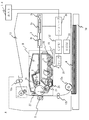
図1、図2を参照して、本発明の実施例に係る画像形成装置の概略構成について説明する。図1は、本発明の実施例に係る画像形成装置の概略構成を示す模式的断面である。図2は、本発明の実施例に係る画像形成装置における制御ブロック図である。本実施例の画像形成装置Aとしては、画像情報に応じて電子写真方式にて例えば、記録用紙、OHPシートなどの記録媒体(記録材)6に画像を形成するレーザビームプリンタが一例として挙げられる。また、本実施例の画像形成装置Aは、詳しくは後述するように、プロセスカートリッジBが画像形成装置Aの装置本体に対して着脱可能とされている。ここで、装置本体とは、画像形成装置AにおいてプロセスカートリッジBを除いた構成部分を指す。なお、本実施例では、感光ドラムに形成したトナー像(現像剤像)を被転写体としての記録材に直接転写する構成の画像形成装置について説明するが、画像形成装置の構成は特に限定されるものではない。例えば、複数の画像形成部で形成したそれぞれ色の異なるトナー像を被転写体としての中間転写体上に重畳転写してカラートナー像を形成し、これを記録材に転写する画像形成装置(カラーレーザプリンタなど)に対しても本発明は適用可能である。
(Example 1)
<Schematic Configuration of Image Forming Apparatus>
1 and 2, a schematic configuration of an image forming apparatus according to an embodiment of the present invention will be described. FIG. 1 is a schematic cross section showing a schematic configuration of an image forming apparatus according to an embodiment of the present invention. FIG. 2 is a control block diagram in the image forming apparatus according to the embodiment of the present invention. As an example of the image forming apparatus A of the present embodiment, a laser beam printer that forms an image on a recording medium (recording material) 6 such as a recording sheet or an OHP sheet in an electrophotographic manner according to image information is given as an example. . In the image forming apparatus A of the present embodiment, the process cartridge B is detachable from the apparatus main body of the image forming apparatus A, as described later in detail. Here, the apparatus main body refers to a component of the image forming apparatus A excluding the process cartridge B. In this embodiment, an image forming apparatus having a configuration in which a toner image (developer image) formed on a photosensitive drum is directly transferred to a recording material as a transfer target is described, but the configuration of the image forming apparatus is not particularly limited. Not something. For example, an image forming apparatus (color image forming apparatus) which forms a color toner image by superimposing and transferring toner images of different colors formed by a plurality of image forming units onto an intermediate transfer body as a transfer receiving body, and transfers this to a recording material (color image forming apparatus) The present invention is also applicable to a laser printer or the like.
画像形成装置Aは、パーソナルコンピュータなどのホスト14に接続されて用いられる。コントローラ部31において、ホスト14からのプリント要求信号並びに画像データを処理し、露光手段であるスキャナ3を制御することで、感光ドラム1上に静電潜像(静電像)を形成する。つまり、画像形成装置Aは、像担持体(回転体)として、図中矢印R1方向に回転駆動される円筒状の感光ドラム1を有している。本実施例において、感光ドラム1は、円筒状の基体であるアルミシリンダの周囲に感光層(電子写真感光体)として膜厚24μmのOPC層が塗工されたものである。この感光ドラム1の良好な画質を維持できる最低感光体膜厚は9μmであり、その時点で感光体寿命となる。
The image forming apparatus A is used by being connected to a
感光ドラム1は、帯電手段である、感光ドラム1に加圧当接されたローラ状の帯電部材、即ち、DC接触帯電ローラ(帯電ローラ)2によって一様に帯電される。本実施例では、帯電ローラ2は、芯金上に導電性ゴム層を設けた構成とされる。本実施例では、詳しくは後述するように、帯電ローラ2には帯電バイアスとして所定の値に固定された直流電圧が電源34から印加され、感光ドラム1の表面を負に一様に帯電させる。帯電ローラ2は感光体ドラム1の回転により、図中矢印R4方向に従動回転する。帯電ローラ2は、感光ドラム1の長手方向(記録媒体6の搬送方向に直交する方向)略全域に亙って当接されている。
The
一様に帯電された感光ドラム1は、露光手段であるスキャナ3からのレーザ光L1により露光され、その表面に静電潜像が形成される。スキャナ3は、レーザ光源3a、ポリゴンミラー3b、レンズ系3cなどを有し、コントローラ部31の制御により、感光ドラム1上を走査露光することができる。本実施例の潜像設定は、感光体膜厚によらず、Vd=−500V、Vl=−100Vとした。
The uniformly charged
その後、この静電潜像は、現像装置4によって現像剤が供給されて、トナー像として可視化される。つまり、現像装置4は、一成分現像剤として負帯電性の非磁性トナー(トナー)22を収容する現像容器21を有する。本実施例では、トナー22には、小粒径化及び低融点化を達成し、且つ、転写効率を向上させるために、重量平均粒径約7μmの略球
形トナーを用いた。
Thereafter, the developer is supplied to the electrostatic latent image by the developing
感光ドラム1と対向する現像容器21の一部は、感光ドラム1の長手方向略全域に亙り開口しており、この開口部にローラ状の現像剤担持体(現像手段)である現像ローラ23が配置されている。現像ローラ23は、現像装置4の図中左上方に位置する感光ドラム1に所定の侵入量となるように押圧、接触され、図中矢印R2方向に回転駆動される。また、その表面は、トナー22との摺擦確率を高め、且つ、トナー22の搬送を良好に行うために、適度な凹凸を有している。
A part of the developing
現像ローラ23の図中右下方には、現像ローラ23への現像剤を供給し、また未現像トナーを現像ローラ23から剥ぎ取る手段として、弾性ローラ24が当接されている。弾性ローラ24は、回転可能に現像容器21に支持されている。また、弾性ローラ24は、現像ローラ23へのトナー供給及び未現像トナーの剥ぎ取り性の点からゴムスポンジローラとし、現像ローラ23と同一方向である図中矢印R3方向に回転駆動する。また、現像装置4は、現像ローラ23に担持させるトナー量を規制する現像剤層厚規制部材として、現像ブレード25を備えている。現像ブレード25は、弾性を有するSUS製の金属薄板で構成され、自由端側の先端近傍を現像ローラ23の外周面に面接触にて当接するように設けられている。弾性ローラ24との摺擦により現像ローラ23上に担持されたトナーは、現像ブレード25との当接部を通過する際に摩擦帯電により電荷付与され、且つ、薄層に規制される。
An
このような構成の現像装置4において、現像ローラ23には、現像バイアスとして所定の値に固定された直流電圧が印加される。本実施例では、感光体膜厚によらず現像バイアスはVdc=−300Vで一定とした。これによって、本実施例では、一様に帯電された感光ドラム1の表面の、負電荷が減衰した露光部を反転現像により現像する。
In the developing
一方、記録媒体6は記録媒体収容部16から供給ローラ12aなどにより分離給送され、レジストローラ12bで一旦停止する。レジストローラ12bは、記録媒体6の記録位置と感光ドラム1へのトナー像の形成タイミングとの同期をとり、転写手段である転写ローラ5と感光ドラム1との対向部(転写部)へと、記録媒体6を送り出す。そして可視化された感光ドラム1上のトナー像は、転写ローラ5の作用によって記録媒体6に転写される。
On the other hand, the
こうしてトナー像を転写された記録媒体6は、定着装置9に搬送される。ここで、記録媒体6上の未定着のトナー像は、熱、圧力よって記録媒体6に永久定着される。その後、記録媒体6は排出ローラ12cなどにより機外に排紙される。
The
一方、記録媒体6にトナー像を転写した後の感光ドラム1は、前露光手段である前露光装置27が発するレーザ光L2により全面露光(全面光照射)されることにより、前回の形成画像によって不均一となった感光ドラム表面の電位が一様に均される。即ち、感光ドラム表面の残留電荷を除去するように感光ドラム表面に光を照射する。前露光装置27(前露光部)は、転写ローラ5よりも感光ドラム回転方向下流側で、帯電ローラ2よりも感光ドラム回転方向上流側の間に配設される。前露光手段の光源としてはLED、ハロゲンランプ等を用いることができる。使用する光源は特に限定されないが、駆動電圧が低く、また装置の小型化が容易という観点から、LEDを用いるのが好ましい。本実施例では、前露光光源としてLEDを用いた。
On the other hand, the
また、転写されずに感光ドラム1上に残留した転写残トナーは、クリーニング手段(クリーナ)10によって清掃する。つまり、クリーナ10は、クリーニング部材であるクリーニングブレード7により転写残トナーを感光ドラム1から掻き取り、廃トナー容器8に
収納する。クリーニングされた感光ドラム1は、上述と同様にして、繰り返し画像形成に供される。
Further, transfer residual toner remaining on the
本実施例では、画像形成装置Aは、像担持体としての電子写真感光体と、この像担持体に作用するプロセス手段とを一体的にカートリッジ化し、このカートリッジを装置本体に対して着脱可能とするプロセスカートリッジ方式とされている。ここで、プロセス手段としては、電子写真感光体を帯電する帯電手段、電子写真感光体に現像剤を供給する現像手段、電子写真感光体をクリーニングするクリーニング手段が含まれる。つまり、プロセスカートリッジとは、次のような構成である。すなわち、帯電手段、現像手段及びクリーニング手段と、電子写真感光体とを一体的にカートリッジ化し、このカートリッジを装置本体に着脱可能とするものである。或いは、帯電手段、現像手段、クリーニング手段のうち少なくとも1つと、電子写真感光体とを一体的にカートリッジ化し、装置本体に対して着脱可能とするものでもよい。或いは、少なくとも現像手段と電子写真感光体とを一体的にカートリッジ化し、このカートリッジを装置本体に対して着脱可能とするものでもよい。 In the present embodiment, the image forming apparatus A is configured such that an electrophotographic photosensitive member as an image carrier and a process unit acting on the image carrier are integrally formed into a cartridge, and the cartridge is detachably mountable to the apparatus main body. Process cartridge system. Here, the processing means includes a charging means for charging the electrophotographic photosensitive member, a developing means for supplying a developer to the electrophotographic photosensitive member, and a cleaning means for cleaning the electrophotographic photosensitive member. That is, the process cartridge has the following configuration. That is, the charging means, the developing means, the cleaning means, and the electrophotographic photosensitive member are integrally formed into a cartridge, and this cartridge is made detachable from the apparatus main body. Alternatively, at least one of the charging unit, the developing unit, and the cleaning unit and the electrophotographic photoreceptor may be integrally formed as a cartridge so as to be detachable from the apparatus main body. Alternatively, at least the developing means and the electrophotographic photosensitive member may be integrally formed into a cartridge, and this cartridge may be detachable from the apparatus main body.
本実施例では、感光ドラム1、帯電ローラ2、現像装置4、クリーナ10が一体的にカートリッジ化され、プロセスカートリッジBを形成し、装置本体13に着脱可能とされている。プロセスカートリッジBは、装置本体13が備えた装着手段15を介して、取り外し可能に装置本体13に装着される。また、上記記録媒体供給ローラ12a、レジストローラ12b、排出ローラ12cなどにより、プロセスカートリッジBに対して記録媒体6を搬送し、また画像形成後の記録媒体6を装置本体13から排出するための、記録媒体搬送手段が構成されている。
In the present embodiment, the
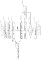
本実施例では、プロセスカートリッジBには記憶手段26(記憶部)が設けられている。記憶手段26としては、例えば、接触不揮発性メモリ、非接触不揮発性メモリ、電源を有する揮発性メモリなど、任意の形態を用いることができる。本実施例では、記憶手段として非接触不揮発性メモリ26がプロセスカートリッジBに搭載されている。非接触不揮発性メモリ26は、メモリ側の情報伝達手段であるアンテナ(図示せず)を有し、無線で画像形成装置本体13が備えた制御手段(CPU)32と通信することで、情報の読み出し及び書き込みが可能である。本実施例では、CPU32は装置本体側の情報伝達手段、メモリ26の情報の読み書き手段の機能を備えている。この記憶手段26には、後述する感光ドラム1の感光体膜厚に関する情報、帯電ローラ2の情報、使用環境に関する情報が記憶される。
以上の構成において、帯電ローラ2への電圧印加に関わる電源34や制御部35、CPU32などの構成が、本発明の電圧印加部に対応する。
In this embodiment, the process cartridge B is provided with a storage unit 26 (storage unit). As the
In the above configuration, the configuration of the
<異常放電現象について>
異常放電は、帯電ローラ2に直流電圧を印加した場合に、帯電ローラ2により形成されるニップよりも感光ドラム回転方向の上流側の長ギャップ部で発生する過放電により帯電電位が過帯電する現象である。帯電電位が過帯電すると、露光後の電位(Vl)も不安定になり、網目状の模様の異常放電画像となる。長ギャップ部では、帯電ローラへの帯電バイアスを上げていくと微弱で時間的に連続であった正常放電が、放電電流が大きく時間的にも空間的にも不連続な断続放電へと劇的に変化する。この異常放電は、正常放電時のタウンゼント放電の範疇であると考えられている。このタウンゼント放電は,電極間の電界およびガスの種類、ガスの圧力、電極材料によって変化する放電現象である。
<About abnormal discharge phenomenon>
The abnormal discharge is a phenomenon in which, when a DC voltage is applied to the charging
大気中の近接放電現象はパッシェン則に従い発生する。この現象は、遊離した電子が電界によって加速され、電極間に存在する分子や電極と衝突して電子、陽イオン及び陰イオンを生成する過程を繰り返す、電子雪崩の拡散現象である。この電子雪崩は電界に従って拡散し、拡散が最終的な放電電荷量を決定する。パッシェン則に従う条件よりも過剰な電
界となれば、局所的な強い放電、すなわち異常放電が発生しやすくなる。
The proximity discharge phenomenon in the atmosphere occurs according to the Paschen rule. This phenomenon is an electron avalanche diffusion phenomenon in which released electrons are accelerated by an electric field and collide with molecules or electrodes existing between electrodes to generate electrons, cations, and anions. The electron avalanche diffuses according to the electric field, and the diffusion determines the final discharge charge amount. If the electric field is excessive than the condition according to Paschen's rule, local strong discharge, that is, abnormal discharge is likely to occur.
この異常放電現象は、以下のような条件において発生しやすい。低温低湿下では、常温常湿下と比較して電極間に存在する分子が少ないことから、パッシェンの法則から導かれる放電開始電圧よりも放電開始電圧が高くなる傾向にある。放電開始電圧が高くなることで、パッシェン則に従う条件よりも過剰な電界になりやすく、低温低湿下では異常放電が発生しやすくなっている。 This abnormal discharge phenomenon is likely to occur under the following conditions. Under low temperature and low humidity, since the number of molecules existing between the electrodes is smaller than that under normal temperature and normal humidity, the discharge start voltage tends to be higher than the discharge start voltage derived from Paschen's law. When the discharge start voltage is increased, an excessive electric field is more likely to occur than under the conditions according to Paschen's rule, and abnormal discharge is likely to occur under low temperature and low humidity.
また、異常放電は、感光ドラム1の膜厚が厚いと発生しやすい。膜厚が厚くなると、静電容量が小さくなるため、所望の帯電電位Vdに必要な帯電電荷量Qが小さくなる。上記のように電子の衝突による電離がなだれ式に発生し、ネズミ算的に荷電粒子が増加することによって、気中が絶縁破壊し一気に大電流が流れると、必要量以上に電荷が溜まることで感光ドラム1の帯電電位は過帯電状態になると推定されている。
Further, abnormal discharge is likely to occur when the thickness of the
また、異常放電は、帯電ローラ2の抵抗が低いと発生しやすい。抵抗が低いローラに放電電流が流れると、抵抗が高いローラに対し、ローラの分担電圧が相対的に低くなる。ローラ分担電圧が低くなることにより、空気層(ギャップ部)の分担電圧が相対的に上がり、感光ドラム1へ流れる放電電流が抵抗の高いローラに比べ大きくなる。よって、抵抗の高いローラに比べ、抵抗の低いローラは異常放電の開始電圧が低く、異常放電が発生しやすいと考えられる。言い換えると、帯電ローラの帯電能に異常放電は依存する。
Abnormal discharge is likely to occur when the resistance of the charging
また、異常放電は、帯電ローラ2による帯電前後での感光ドラム1の表面電位の変化によって発生しやすくなる場合がある。具体的には、帯電ローラ2による帯電直前の感光ドラム1の表面電位(以下、帯電前電位)と、帯電直後の感光ドラム1の表面電位との電位差が大きいと、空気層(ギャップ部)の電界が強くなり、放電電流量が多くなり異常放電が発生しやすい。前露光装置27は、前回の形成画像によって不均一となった感光ドラム1表面の電位を一様に均すために、帯電ローラ2で帯電する前に感光ドラム1表面を全面露光する。そのため、前露光なしの構成に比べて、前露光ありの構成は帯電前電位と帯電電位との電位差が大きい。
Further, the abnormal discharge may be easily generated due to a change in the surface potential of the
また、帯電前電位と帯電電位(帯電直後の感光ドラム1の表面電位)との電位差は、帯電電位Vdが高いほど大きくなるため、帯電ローラ2に印加する帯電バイアスが高いほど、異常放電が発生しやすい。
In addition, since the potential difference between the pre-charging potential and the charging potential (the surface potential of the
<異常放電の発生状況>
図3は、現像位置での感光ドラム1の表面電位の時間推移を示すものである。図3(a)は異常放電発生時、図3(b)は異常放電が発生していないときをそれぞれ示している。プリント信号が入力されると、前回転動作が始まり、感光ドラム1が回転し、帯電バイアスが印加される。iは、帯電バイアスが印加されたときの感光ドラム1の帯電電位である。iiは、前露光装置27による照射後の感光ドラム1の帯電電位Vdである。iiiは、前露光装置27の照射が開始されたタイミングである。本実施例では、長寿命化の観点から、通常、前露光装置27の照射時間を可能な限り短くするべく像露光直前に前露光装置27の照射を開始している。
<Status of abnormal discharge>
FIG. 3 shows a time transition of the surface potential of the
図3に示すように、異常放電が発生する場合、前露光装置27の照射が開始された直後に感光ドラム1において前露光を受けた領域における表面電位がVdよりも高く、過帯電する(iV)。その後、時間の経過とともに、異常放電は収束し、正常の帯電電位Vdとなる。感光ドラム1が過帯電している状態で露光すると、露光後の電位(Vl)も不安定になり、網目状の異常放電画像となる。一方、異常放電が発生しない場合は、前露光27の照射が開始された直後においても、所望の帯電電位Vdとなるため、異常放電画像は発
生しない。
As shown in FIG. 3, when an abnormal discharge occurs, immediately after the irradiation of the
従って、異常放電が発生する場合には、異常放電が終了後の正常の帯電電位Vdになってから露光すれば、異常放電画像の発生を未然に防ぐことができる。画像形成前の前露光点灯時間を異常放電画像が発生しない時間まで一律に長くすれば画像発生は回避できるが、前露光時間が長くなるとドラム削れ等のトレードオフが発生する。そこで、より具体的には、異常放電時間を検知し、異常放電している場合のみ前露光27の照射開始を早める、もしくは露光開始を遅らせることで、異常放電画像の発生を回避しつつ、長寿命化を実現することができる。
Therefore, in the case where abnormal discharge occurs, exposure can be performed after reaching the normal charging potential Vd after the end of the abnormal discharge, thereby preventing occurrence of an abnormal discharge image. Image generation can be avoided if the pre-exposure lighting time before image formation is uniformly increased to a time at which no abnormal discharge image occurs, but a trade-off such as drum scraping occurs when the pre-exposure time is increased. Therefore, more specifically, the abnormal discharge time is detected, and the irradiation start of the
<異常放電時間の検知方法について>
次に異常放電時間(異常放電(過帯電状態)の持続時間)の検知方法について説明する。本実施例では、感光ドラム1の膜厚に関する情報と、使用環境に関する情報と、を用いて、異常放電時間を算出(取得)する。本実施例において、異常放電時間の取得に関わる構成が、本発明の取得部に対応する。
<How to detect abnormal discharge time>
Next, a method of detecting an abnormal discharge time (duration of abnormal discharge (overcharged state)) will be described. In the present embodiment, the abnormal discharge time is calculated (acquired) using information on the film thickness of the
図4は、感光ドラム1の膜厚の違いと使用環境(温度、湿度)の違いとにより、最大異常放電時間がどのように変化するのかを示したグラフである。なお、帯電電位はVd=−500Vである。このグラフから、高温高湿環境(H/H)である温度30℃、湿度80%では異常放電は発生していないが、低温低湿環境(L/L)である温度15℃、湿度10%では異常放電が発生する。また、低温低湿環境(L/L)において、感光ドラム1の膜厚が厚くなると、異常放電が発生し、膜厚が厚くなるほど異常放電時間が長くなっていることがわかる。また、異常放電時間は、帯電ローラ2の抵抗値が低いほど長くなる。
FIG. 4 is a graph showing how the maximum abnormal discharge time changes depending on the difference in the film thickness of the
そこで、これらの測定データ(異常放電時間と感光ドラムの膜厚との関係、異常放電時間と使用環境との関係)に基づいて、異常放電時間を算出する近似曲線を求めて、そのデータを予め画像形成装置本体側のROM33に格納する。ここで、帯電ローラ2の抵抗値は製法上、多少のばらつきがあるため、本実施例では、バラツキの中で抵抗値が最小の帯電ローラでの結果を採用した。異常放電時間の検知は、記憶手段26に記憶された感光ドラム1の膜厚に関する情報と温度、湿度の情報に対応するROM33に格納された近似曲線上のデータを採用することにより異常放電時間を算出することができる。なお、近似曲線の求め方としては、線形近似、指数近似、多項式近似、累計近似、移動平均近似などの統計手法があるが、特に制約はなく、適宜最適なものを用いることができる。
Therefore, based on these measurement data (the relationship between the abnormal discharge time and the film thickness of the photosensitive drum and the relationship between the abnormal discharge time and the use environment), an approximate curve for calculating the abnormal discharge time is obtained, and the data is obtained in advance. It is stored in the
<感光ドラム1の膜厚に関する情報、使用環境に関する情報>
感光ドラム1の膜厚に関する情報は以下の方法で算出する。前述したように、感光体膜厚は、放電によって感光ドラム1の表面が劣化し、記録媒体6の通過(通紙)或いはクリーニング部材7の当接によって感光ドラム1の表面が削り取られることにより減少する。本実施例の画像形成装置Aでは、感光ドラム1における感光体膜厚の減少は、帯電バイアス印加時間と相関がある。また、この帯電バイアス印加時間は、画像形成枚数に比例している。従って、感光ドラム1における感光体膜厚の減少率は、画像形成枚数の一次関数として表すことができる。
<Information on film thickness of
Information on the film thickness of the
使用環境に関する情報は以下の方法で算出する。本実施例の画像形成装置Aは、環境検知手段としての環境センサ(温度湿度センサ)28を装置本体に備えており、所定時間毎に温度Pと湿度Qを検知し、記憶手段26の使用環境に関する情報を書き換える。本実施例においては、プロセスカートリッジBに搭載した記憶手段26に、感光体膜厚に関する情報として画像形成枚数(P)、使用環境に関する情報として温度及び湿度を記憶する。そして、これら2つの情報を用いて、上述の方法で異常放電時間を算出して、前露光装置27による照射開始から像露光開始までの時間を変化させる。なお、感光体膜厚に関する
情報としては、上記画像形成枚数の他、感光ドラム1の回転数、通紙枚数(画像形成装置内を通過した記録材の数)、帯電時間(帯電バイアス印加時間)などが挙げられ、いずれの情報を選択しても構わない。
Information on the usage environment is calculated by the following method. The image forming apparatus A according to the present embodiment includes an environment sensor (temperature / humidity sensor) 28 as an environment detecting unit in the main body of the apparatus. Rewrite information about In the present embodiment, the
<前露光装置の照射開始とスキャナの露光開始の間隔の制御方法について>
図5のフローチャートを参照して、前露光装置27の照射開始からスキャナ3(露光部)の露光開始までの時間を変化させる方法について説明する。プロセスカートリッジBは、記憶手段26を具備しており、記憶手段26には、プロセスカートリッジBを用いて行った画像形成枚数と、温度、湿度が記憶されている。ホスト14からプリント信号が入力されると(S101)、CPU32は、プロセスカートリッジBに搭載された記憶手段26と通信を行い、そのプロセスカートリッジBの画像形成枚数(P)と温度、湿度を読み込む(S102)。次に、CPU32は、画像形成枚数、温度、湿度に応じた異常放電時間が予め格納された、画像形成装置本体側ROM33の内容と、上述のようにCPU32に読み込んだ画像形成枚数の値(P)、温度、湿度とを比較する(S103)。次いで、CPU32は、前露光装置27の照射開始からスキャナ3の露光開始までの時間を制御する制御部35により、前露光装置27の照射開始とスキャナ3の像露光開始の時間を設定し、画像形成動作に移行する(S104)。
<About the control method of the interval between the irradiation start of the pre-exposure device and the exposure start of the scanner>
A method of changing the time from the start of irradiation of the
図6は、前露光装置27の照射開始(第1タイミング)からスキャナ3の像露光開始(第2タイミング)までのタイミングチャートである。画像形成動作が始まると、感光ドラム1が回転し、所定の帯電バイアスが印加される。その後、前露光装置27が照射を開始し、スキャナ3が像露光を開始する。異常放電が発生していない場合は、前露光装置27はスキャナ3が像露光を開始する直前に照射を開始する。前露光装置27は、スキャナ3による像露光の位置よりも感光ドラム1の回転方向上流側に配置されているため、前露光位置と露光位置との距離の分だけ、前露光装置27の照射タイミングはスキャナ3の像露光タイミングよりも早めとなる。一方、異常放電が発生している場合には、スキャナ3の像露光開始時間は固定し、異常放電時間だけ前露光装置27の照射開始を早める。すなわち、スキャナ3の像露光開始時間が、異常放電が終了するタイミング(第3タイミング)よりも後となるように、前露光装置27の照射開始のタイミングを変更する。
FIG. 6 is a timing chart from the start of irradiation of the pre-exposure device 27 (first timing) to the start of image exposure of the scanner 3 (second timing). When the image forming operation starts, the
画像形成動作が終了すると画像形成枚数のカウントを1増加し(S105)、プロセスカートリッジBの記憶手段26の画像形成枚数のカウントを書き変える(S106)。続いて、連続プリントの要求があるかを判断し(S107)、要求がない場合はプリント終了動作に移行し(S108)、要求がある場合は、連続プリントの要求がなくなるまで、S103〜S107の動作を繰り返す。
When the image forming operation is completed, the count of the number of image formation is increased by 1 (S105), and the count of the number of image formation in the
<効果の確認>
本実施例の効果を確認するために、上述のような制御を行った本実施例の画像形成装置Aと、本実施例の制御を行わない、従来の制御を行う比較例1、2の画像形成装置を用いて、50000枚の画像形成を行った。それぞれにおける異常放電画像と感光ドラムの削れに起因する画像不良であるスジの発生有無について比較した。確認は、異常放電が発生しやすくかつ感光ドラム1が削れやすい低温低湿環境(温度15℃、湿度10%)において行った。
<Confirmation of effect>
In order to confirm the effect of the present embodiment, the image forming apparatus A of the present embodiment that performs the above-described control and the images of Comparative Examples 1 and 2 that perform the conventional control without performing the control of the present embodiment. Using a forming apparatus, 50,000 images were formed. The abnormal discharge image in each case was compared with the presence or absence of streaks, which are image defects caused by scraping of the photosensitive drum. The confirmation was performed in a low-temperature and low-humidity environment (temperature: 15 ° C., humidity: 10%) where abnormal discharge easily occurs and the
比較例としては、スキャナ3の像露光直前に前露光装置27の照射を開始する構成の比較例1と、比較例1に対し、スキャナ3の像露光開始時間から常に一定の時間間隔Tだけ前に前露光装置27の照射を開始する比較例2の2つを対象とした。時間間隔Tは、異常放電が最も発生しやすい低温低湿環境における最大異常放電時間とした。
As a comparative example, the comparative example 1 in which the irradiation of the

表1は、上記比較実験の結果を本実施例と従来例とで比較して示している。表1から明らかなように本実施例に従う制御を行う場合、画像形成枚数によらず長期の使用を通して、異常放電画像の発生はなく、良好な結果であった。また、感光ドラムの削れに起因するスジの発生もなかった。一方、比較例1においては、感光ドラムの削れに起因するスジの発生はなかったものの、異常放電画像が発生した。また、比較例2においては、異常放電画像の発生はなかったものの、感光ドラムの削れに起因するスジが発生した。 Table 1 shows the results of the above-mentioned comparative experiment in comparison between the present embodiment and the conventional example. As is clear from Table 1, when the control according to the present embodiment was performed, no abnormal discharge image was generated over a long period of use irrespective of the number of formed images, and good results were obtained. In addition, no streaks were generated due to scraping of the photosensitive drum. On the other hand, in Comparative Example 1, although there was no streak caused by scraping of the photosensitive drum, an abnormal discharge image occurred. Further, in Comparative Example 2, although no abnormal discharge image was generated, streaks due to scraping of the photosensitive drum were generated.
以上、本実施例によれば、異常放電時間の長さに応じて、前露光装置27の照射開始からスキャナ3の像露光開始までの時間を最適化していくことで、長期の使用を通して、異常放電画像の発生を回避しつつ、長寿命化することができる。異常放電時間は、感光ドラム1の感光体膜厚に関する情報のうちの一つである画像形成枚数と、使用環境に関する情報としての温度及び湿度と、から取得することができる。これらの情報は、プロセスカートリッジに搭載された記憶手段26に記憶する。
As described above, according to the present embodiment, the time from the start of irradiation of the
本実施例では、異常放電時間を検知し、異常放電している場合のみ前露光装置27の照射開始を早めたが、時間調整の方法としてはこれに限定されない。例えば、前露光装置27の照射開始からスキャナ3の像露光開始までの時間が長くなればよく、前露光装置27の照射開始時間は固定して、スキャナ3の像露光開始の時間を遅らせてもよい。あるいは、前露光装置27の照射開始時間を早めるとともに、スキャナ3の像露光開始の時間を遅らせて、所望の時間間隔を確保することができるように制御してもよい。
In this embodiment, the abnormal discharge time is detected, and the irradiation start of the
なお、本実施例では、記憶手段26をプロセスカートリッジBに設けた。これにより、プロセスカートリッジ自身に感光体膜厚に関する情報や、温度と湿度を保持させ得る。従って、例えば、寿命に達していないプロセスカートリッジBを装置本体13に対して交換使用するような場合でも、常に各プロセスカートリッジBに即した感光体膜厚に関する情報や、温度と湿度を装置本体で認識することができ、極めて有利である。しかし、本発明が適用可能な態様は、この態様に限定されるものではなく、本発明の原理は、装置本体に記憶手段を設ける場合にも適用でき、本実施例と同様の効果を得ることができる。
In this embodiment, the storage means 26 is provided in the process cartridge B. As a result, the process cartridge itself can hold information on the thickness of the photoconductor, temperature and humidity. Therefore, for example, even when the process cartridge B which has not reached the end of its life is exchanged for the apparatus
また、本発明は、画像形成装置がプロセスカートリッジ方式でない構成の場合にも適用することができ、本実施例と同様の効果を奏し得る。この場合、記憶手段を装置本体に設け、感光体膜厚や、温度と湿度に関する情報を記憶させる。そして、例えば、感光ドラムを個別に交換した場合などに、記憶手段内の感光体膜厚に関する情報や、温度と湿度をリセットするなどすればよい。 Further, the present invention can be applied to a case where the image forming apparatus is not of a process cartridge type, and can provide the same effects as the present embodiment. In this case, a storage unit is provided in the main body of the apparatus, and stores information relating to the thickness of the photoreceptor and the temperature and humidity. Then, for example, when the photosensitive drums are individually exchanged, the information on the thickness of the photosensitive member in the storage means, or the temperature and humidity may be reset.
また、前述のように帯電電位Vdが高くなると、異常放電しやすくなる。本実施例の潜像設定は、感光体の感光層の膜厚によらず、Vd=−500Vとしたが、使用期間に応じて帯電電位Vdが変わるような場合には、帯電電位Vdに応じて、異常放電時間を補正すればよい。また、本実施例では、感光ドラム1の膜厚に関する情報と使用環境に関する情報の2つを用いて異常放電時間を算出(取得)したが、いずれか一方の情報に基づいて算出してもよい。また、異常放電時間を直接的に算出する方法だけではなく、帯電ローラ2に流れる帯電電流などを測定して、電流が所定の範囲を超えた時間に基づいて、前露光装置27の照射開始からスキャナ3の像露光開始までの時間を変化させてもよい。
As described above, when the charging potential Vd is high, abnormal discharge is likely to occur. In the present embodiment, the latent image is set at Vd = −500 V regardless of the thickness of the photosensitive layer of the photosensitive member. However, when the charging potential Vd changes according to the use period, the latent image is set according to the charging potential Vd. Then, the abnormal discharge time may be corrected. Further, in the present embodiment, the abnormal discharge time is calculated (acquired) using the information on the film thickness of the
(実施例2)
異常放電時間は、帯電ローラ2の抵抗値に依存する。前述したように、異常放電時間は、帯電ローラ2の抵抗値が低いほど長くなり、高くなると短くなる。そこで、本発明の実施例2では、感光ドラム1の膜厚に関する情報と使用環境に関する情報に加えて、帯電ローラ2の帯電能に関する情報に基づいて、異常放電時間を算出することを特徴とする。これ以外の点は、実施例1と同じであり、実施例2において実施例1と同様の構成については説明を省略する。
(Example 2)
The abnormal discharge time depends on the resistance value of the charging
帯電ローラ2の帯電能は、帯電ローラ2の抵抗値と相関がある。抵抗値は、長期の使用によって変動するため、帯電バイアス印加時間や積算帯電電流量(帯電ローラに流れる電流量の積算値)などに比例している。また、温度や湿度によっても抵抗値は変動する。本実施例では、新品時の帯電ローラ2の抵抗値を記憶手段26に記憶する。
The charging ability of the charging
本実施例では、異常放電時間と感光ドラムの膜厚との関係、異常放電時間と帯電ローラの抵抗値との関係、異常放電時間と使用環境との関係から近似曲線を求めて、そのデータを予め画像形成装置本体側のROM33に格納しておく。異常放電時間の検知は、記憶手段26に記憶された感光ドラム1の膜厚に関する情報と、温度、湿度の情報と、帯電ローラの抵抗値に対応するROM33に格納された近似曲線上のデータを採用することにより異常放電時間を算出する。
In this embodiment, an approximate curve is obtained from the relationship between the abnormal discharge time and the thickness of the photosensitive drum, the relationship between the abnormal discharge time and the resistance value of the charging roller, and the relationship between the abnormal discharge time and the use environment, and the data is obtained. It is stored in advance in the
以上、本実施例によれば、感光ドラム1の感光体膜厚に関する情報のうちの一つである画像形成枚数と、温度と湿度と、帯電ローラ2の抵抗値を、プロセスカートリッジBに搭載された記憶手段26に記憶する。記憶手段26に記憶された情報に対応して、前露光装置27の照射開始からスキャナ3の像露光開始までの時間を最適化していくため、長期使用を通して、異常放電画像の発生を回避しつつ、長寿命化することができる。
As described above, according to the present embodiment, the number of images to be formed, the temperature and the humidity, and the resistance value of the charging
なお、本実施例では、帯電ローラ2の帯電能に関する情報として、新品時の抵抗値を採用し、異常放電時間を算出する。帯電ローラ2の帯電能に関する情報の利用の仕方はこれに限定されるものではなく、例えば、帯電バイアス印加時間や積算帯電電流量、温度、湿度などの情報から、抵抗値の長期使用による変動、環境変動も考慮して、異常放電時間を補正してもよい。
In this embodiment, the abnormal discharge time is calculated by using a resistance value at the time of a new product as information on the charging ability of the charging
(実施例3)
本発明の実施例3では、帯電ローラ2に流れる帯電電流を測定し、測定電流値が所定の範囲を超えた時間に基づいて、前露光装置27の照射開始からスキャナ3の像露光開始までの時間を変化させることを特徴とする。実施例3において実施例1、2と共通する構成については説明を省略する。実施例3においてここで説明しない事項は、実施例1、2と同様である。
(Example 3)
In the third embodiment of the present invention, the charging current flowing through the charging
<異常放電時間の検知方法について>
本実施例では、帯電ローラ2に流れる帯電電流を測定し、測定された帯電電流値の値に
基づいて、異常放電時間を算出(取得)する。帯電ローラ2に流れる帯電電流を測定するため、本実施例では図2に示すように帯電電流検知部36を有する。帯電電流検知部36は、CPU32から信号を送られることで帯電ローラ2にDC電圧を印加しながら帯電電流値を検知する。
図7は、異常放電が生じた場合の帯電電流値の時間推移を示す図である。帯電バイアス印加直後は異常放電によって帯電電流値が正常な値より大きくなるが、やがて異常放電は収束して正常な帯電電流値に戻る。
<How to detect abnormal discharge time>
In this embodiment, the charging current flowing through the charging
FIG. 7 is a diagram showing a time transition of a charging current value when an abnormal discharge occurs. Immediately after the application of the charging bias, the charging current value becomes larger than the normal value due to the abnormal discharge. However, the abnormal discharge eventually converges and returns to the normal charging current value.
図8は、図7で表記した帯電バイアス印加直後であるA点における帯電電流値と帯電バイアスの関係を示す図である。A点では帯電バイアスが増加すると、あるバイアス値で異常放電によって相転移的に帯電電流値が増加している。また、図8には、図7で表記したB点における帯電電流値と帯電バイアスの関係も表している。B点では異常放電が収束しており、正常な帯電電電流値となっている。B点では帯電バイアスと帯電電流は直線の関係にある。また、A点における異常放電が発生するバイアス以下の帯電バイアスの直線と一致している。このことから、異常放電が発生するバイアスより低いバイアスでのA点における測定点から正常な帯電電流と帯電バイアスの関係が分かる。 FIG. 8 is a diagram showing the relationship between the charging current value and the charging bias at point A immediately after the application of the charging bias shown in FIG. At the point A, when the charging bias increases, the charging current value increases in a phase transition due to abnormal discharge at a certain bias value. FIG. 8 also shows the relationship between the charging current value and the charging bias at point B shown in FIG. At the point B, the abnormal discharge has converged, and the charging current has a normal value. At point B, the charging bias and the charging current have a linear relationship. Further, it coincides with a straight line of a charging bias equal to or lower than a bias at which abnormal discharge occurs at point A. From this, the relationship between the normal charging current and the charging bias can be determined from the measurement point at the point A at a bias lower than the bias at which the abnormal discharge occurs.
本実施例では、A点(帯電バイアス印加直後)における異常放電が発生するバイアス以下での帯電バイアス値2点の測定から近似直線を引き、この近似直線から得られる帯電電流値を正常な帯電電流値とした。近似直線の求め方はこの限りでなく2点以上の測定点で求めればよく、点数を増やせば精度を上げる事が出来る。そして、正常な帯電電流と帯電バイアスの関係から所望の帯電バイアス時の正常な帯電電流値を把握することが可能になる。 In this embodiment, an approximate straight line is drawn from the measurement of two points of the charging bias value below the bias at which abnormal discharge occurs at the point A (immediately after the application of the charging bias), and the charging current value obtained from this approximate straight line is used as the normal charging current. Value. The method of obtaining the approximate straight line is not limited to this, but may be obtained at two or more measurement points, and the accuracy can be improved by increasing the number of points. Then, the normal charging current value at the time of a desired charging bias can be grasped from the relationship between the normal charging current and the charging bias.
異常放電時間の検知は、画像形成時の帯電バイアス印加時に帯電ローラ2に流れる帯電電流値と正常な放電時に帯電ローラ2に流れる帯電電流値とを比較することで算出することができる。
図9は、所望の帯電バイアス印加時に流れる帯電電流値から近似直線で得られる正常な帯電電流値を引いた値の時間推移を示している。本実施例では帯電バイアス印加時点(第4タイミング)から帯電電流値がある所定の電流値内(閾値範囲内)(δI)になるまでの時間(第5タイミング)を異常放電時間(T0)と判断した。なお、本実施例では、帯電ローラ2に流れる帯電電流Icを検知したが、転写電流、ドラムアース電流を計測しても良い。この方法で異常放電時間を算出して、前露光装置27の照射開始からスキャナ3の像露光開始までの時間を変化させる。
The detection of the abnormal discharge time can be calculated by comparing a charging current value flowing through the charging
FIG. 9 shows a time transition of a value obtained by subtracting a normal charging current value obtained by an approximate straight line from a charging current value flowing when a desired charging bias is applied. In the present embodiment, the time (fifth timing) from when the charging bias is applied (fourth timing) to when the charging current value falls within a predetermined current value (within a threshold value range) (δI) is defined as an abnormal discharge time (T0). It was judged. In this embodiment, the charging current Ic flowing through the charging
<前露光装置の照射開始とスキャナの露光開始の間隔の制御方法について>
図10のフローチャートを参照して、本実施例における前露光装置27の照射開始からスキャナ3の像露光開始までの制御方法について説明する。プロセスカートリッジBは、記憶手段26を具備しており、記憶手段26には、プロセスカートリッジBを用いて行った画像形成枚数(P)と温度、湿度が記憶されている。ホスト14からプリント信号が入力されると(S201)、CPU32は、プロセスカートリッジBに搭載された記憶手段26と通信を行い、そのプロセスカートリッジBの画像形成枚数(P)と温度、湿度を読み込む(S202)。
<About the control method of the interval between the irradiation start of the pre-exposure device and the exposure start of the scanner>
A control method from the start of irradiation of the
次に、CPU32は、異常放電時間TOを検知するタイミングかどうかを確認する(S203)。S203では、温度・湿度が事前に決められた閾値以内であるか、画像形成枚数(P)が事前に決められた所定の枚数と一致したかを確認する。本実施例では、0枚目と2000枚目ごとに1回を枚数による検知タイミング、温度・湿度から算出される絶対水分量が前回の検知値から±1g/m3変化する時点を温度・湿度による検知タイミングとしている。ただし、この限りでなく画像形成装置の寿命や帯電ローラ2の帯電能等に合
わせて適宜タイミングを設定すれば良い。
Next, the
温度・湿度が閾値を超えている、もしくは事前に決められた所定の枚数と一致する場合、検知タイミングとなり、帯電電流の検知を実施して正常な帯電電流と帯電バイアスの関係を求める(S204)。次いで、所望の帯電バイアスにおける帯電電流値を測定し(S205)、所望の帯電バイアス印加時に流れる帯電電流値と正常な放電時の帯電電流値とを比較することで異常放電時間TOを算出(取得)し、記憶部に書き込む(S206)。また、事前に決められた所定の枚数と一致しない、かつ温度・湿度が閾値以内の場合は、記憶手段から異常放電時間TOを読み込む(S207)。そして、異常放電時間TOの値に基づいて、前露光装置27の照射開始からスキャナ3の像露光開始までの時間を制御する制御部35で前露光27の照射開始と像露光開始の時間を設定し、画像形成動作に移行する(S208)。
If the temperature / humidity exceeds the threshold value or coincides with a predetermined number of sheets determined in advance, the detection timing comes, and the charging current is detected to obtain a normal relationship between the charging current and the charging bias (S204). . Next, the charging current value at the desired charging bias is measured (S205), and the abnormal discharging time TO is calculated (obtained) by comparing the charging current value flowing when the desired charging bias is applied with the charging current value during normal discharging. ) And write it to the storage unit (S206). If the number does not match the predetermined number and the temperature / humidity is within the threshold, the abnormal discharge time TO is read from the storage unit (S207). Then, based on the value of the abnormal discharge time TO, the
ここで、異常放電時間TOの値に基づいて前露光装置27の照射開始からスキャナ3の像露光開始までの時間を設定する際には、温度・湿度の閾値内での異常放電時間の変化を考慮する必要がある。本実施例では、初期膜厚状態の感光ドラム1と、バラツキの中で抵抗値が最小の帯電ローラ2における絶対水分量と、異常放電時間との関係から、絶対水分量が1g/m3変化した場合における異常放電時間の最大変化量を事前に求めておく。その最大変化量を異常放電時間TOに加えた値に基づいて、前露光装置27の照射開始からスキャナ3の像露光開始までの時間を設定する。
Here, when setting the time from the start of irradiation of the
画像形成動作が終了すると画像形成枚数のカウントを1増加し(S209)、プロセスカートリッジBの記憶手段26の画像形成枚数のカウントを書き変える(S210)。続いて、連続プリントの要求があるかを判断し(S211)、要求がない場合はプリント終了動作に移行し(S212)、要求がある場合は、連続プリントの要求がなくなるまで、S203〜S211の動作を繰り返す。
When the image forming operation is completed, the count of the number of image formation is increased by 1 (S209), and the count of the number of image formation in the
以上、本実施例によれば、帯電ローラ2に流れる帯電電流を検知し、検知した帯電電流値に基づいて異常放電時間を算出することができる。これにより、実施例1、2と同様、前露光装置27の照射開始からスキャナ3の像露光開始までの時間を最適化することができ、異常放電画像の発生を回避しつつ、長寿命化することができる。
As described above, according to the present embodiment, the charging current flowing through the charging
(実施例4)
本発明の実施例4は、前露光装置27の照射開始とスキャナ3の露光開始の間隔の制御方法が、上記実施例3と異なる構成となっている。具体的には、実施例4は、実施例3のように異常放電時間を検知するか否かの判断は行わず、画像形成動作の実行中に異常放電時間の取得を行うことを特徴とする。その他の構成は上記実施例3と同様である。実施例4においてここで説明しない事項は、実施例1〜3と同様である。
(Example 4)
The fourth embodiment of the present invention is different from the third embodiment in the method of controlling the interval between the irradiation start of the
<前露光装置の照射開始とスキャナの露光開始の間隔の制御方法について>
図11のフローチャートを参照して、本発明の実施例4における異常放電画像を回避する制御について説明する。本実施例では、前露光装置27の照射開始からスキャナ3の露光開始までの時間を以下のように変化させる。
<About the control method of the interval between the irradiation start of the pre-exposure device and the exposure start of the scanner>
The control for avoiding the abnormal discharge image according to the fourth embodiment of the present invention will be described with reference to the flowchart of FIG. In the present embodiment, the time from the start of irradiation of the
ホスト14からプリント信号が入力されると(S301)、帯電電流の検知を実施して正常な帯電電流と帯電バイアスの関係を求める(S302)。次いで、所望の帯電バイアスにおける帯電電流値を測定し(S303)、所望の帯電バイアス印加時に流れる帯電電流値と、正常な放電時の帯電電流値とを比較することで異常放電時間T0を算出する(S304)。次に、異常放電時間T0の値に基づいて、制御部35で前露光装置27の照射開始とスキャナ3の像露光開始の時間を設定し、画像形成動作に移行する(S305)。
When a print signal is input from the host 14 (S301), the charging current is detected to determine the normal relationship between the charging current and the charging bias (S302). Next, a charging current value at a desired charging bias is measured (S303), and an abnormal discharging time T0 is calculated by comparing the charging current value flowing at the time of applying the desired charging bias with the charging current value at the time of normal discharging. (S304). Next, based on the value of the abnormal discharge time T0, the
図6に示すように、画像形成動作が始まると、感光ドラム1が回転し、所定の帯電バイアスが印加される。その後、前露光装置27が照射を開始し、スキャナ3が像露光を開始する。異常放電が発生していない場合は、前露光装置27はスキャナ3が像露光を開始する直前に照射を開始する。前露光装置27は、スキャナ3の像露光位置よりも感光ドラム1の回転方向上流側に配置されているため、前露光位置と露光位置との距離の分だけ、前露光装置27の照射開始タイミングは、スキャナ3の像露光開始タイミングより早めになる。一方、異常放電が発生している場合には、スキャナ3の像露光開始時間は固定し、異常放電時間だけ前露光装置27の照射開始を早める。
As shown in FIG. 6, when the image forming operation starts, the
この際、本実施例では、帯電ローラ2に流れる帯電電流を検知する帯電電流検知部36により、前露光照射開始から画像形成動作終了まで帯電電流をモニターし、正常な帯電電流値までに回復するまでの時間(異常放電時間)を測定する(S306)。画像形成動作が終了すると、プロセスカートリッジBの記憶手段26の異常放電時間TOを書き変える(S307)。続いて、連続プリントの要求があるかを判断し(S308)、要求がある場合は、異常放電時間TOを記憶手段から読み込み(S309)、連続プリントの要求がなくなるまでS305からS309の動作を繰り返す。要求がない場合はプリント終了動作に移行する(S310)。
At this time, in the present embodiment, the charging current is monitored from the start of the pre-exposure irradiation to the end of the image forming operation by the charging current detecting
以上、本実施例によれば、帯電ローラ2に流れる帯電電流を検出し、電流値が所定の範囲を超える変動域の時間に基づいて異常放電時間を算出し、算出した異常放電時間をもとに、前露光装置27の照射開始からスキャナ3の像露光開始までの時間を最適化する。これにより、異常放電画像の発生を回避することができる。
As described above, according to the present embodiment, the charging current flowing through the charging
本実施例では、異常放電時間を検知し、異常放電している場合のみ前露光装置27の照射開始を早めたが、時間調整の方法としてはこれに限定されない。例えば、前露光装置27の照射開始からスキャナ3の像露光開始までの時間が長くなればよく、前露光装置27の照射開始時間は固定して、スキャナ3の像露光開始の時間を遅らせてもよい。あるいは、前露光装置27の照射開始時間を早めるとともに、スキャナ3の像露光開始の時間を遅らせて、所望の時間間隔を確保することができるように制御してもよい。なお、感光ドラム1は一定の速度で回転するため、時間調整がなされることで、前露光開始のタイミングから像露光開始のタイミングまでの間に感光ドラム1が回転する回数(あるいは走行距離)が変わることになる。
In this embodiment, the abnormal discharge time is detected, and the irradiation start of the
(実施例5)
異常放電時間TOは、連続プリント中(複数の記録材に連続的に画像形成を行う間)に検知することも可能である。本発明の実施例5では、連続プリント時に異常放電時間の検知を逐次実行し、その値を使用して、前露光装置27の照射開始からスキャン3の像露光開始までの時間を逐次変化させる。実施例5において上記各実施例と共通する構成については説明を省略する。実施例5においてここで説明しない事項は、上記各実施例と同様である。
(Example 5)
The abnormal discharge time TO can be detected during continuous printing (during continuous image formation on a plurality of recording materials). In the fifth embodiment of the present invention, the detection of the abnormal discharge time is sequentially performed during the continuous printing, and the time from the start of the irradiation of the
<前露光の照射開始と露光開始の間隔の制御方法について>
図12のフローチャートを参照して、実施例5における前露光装置27の照射開始からスキャナ3の露光開始までの時間を変化させる方法について説明する。本実施例では、帯電バイアスと帯電電流との関係、感光ドラムの膜厚と帯電電流との関係、使用環境と帯電電流との関係、から近似曲線を求めて、そのデータを予め画像形成装置本体側のROM33に格納している。なお、近似曲線の求め方としては、線形近似、指数近似、多項式近似、累計近似、移動平均近似などの統計手法があるが、特に制約はなく、適宜最適なものを用いることができる。
<About the control method of the interval between the irradiation start of the pre-exposure and the exposure start>
A method for changing the time from the start of irradiation of the
プロセスカートリッジBは、記憶手段26を具備しており、記憶手段26には、プロセスカートリッジBを用いて行った画像形成枚数(P)と温度、湿度と異常放電時間T0が記憶されている。ホスト14からプリント信号が入力されると(S601)、CPU32は、プロセスカートリッジBに搭載された記憶手段26と通信を行い、そのプロセスカートリッジBの画像形成枚数(P)と温度、湿度を読み込む(S602)。次に、CPU32は、画像形成枚数、温度、湿度に応じた異常放電時間が予め格納された画像形成装置本体側ROM33の内容と、上述のようにCPU32に読み込んだ画像形成枚数の値(P)、温度、湿度とを比較する(S603)。さらに、CPU32は、画像形成時の帯電バイアス印加時の異常放電時間を算出する(S603)。
The process cartridge B includes a
次いで、CPU32は、前露光装置27の照射開始からスキャナ3の露光開始までの時間を制御する制御部35により、前露光装置27の照射開始とスキャナ3の像露光開始の時間を設定し、画像形成動作に移行する(S604)。この際、本実施例では帯電ローラ2に流れる帯電電流を検知する帯電電流検知部36により、前露光照射開始から画像形成動作終了まで帯電電流をモニターし、正常な帯電電流値までに回復するまでの時間(異常放電時間)を測定する(S605)。
Next, the
画像形成動作が終了すると画像形成枚数のカウントを1増加し(S606)、プロセスカートリッジBの記憶手段26の画像形成枚数のカウントと異常放電時間TOを書き変える(S607)。続いて、連続プリントの要求があるかを判断し(S608)、要求がある場合は、異常放電時間TOを記憶手段から読み込み(S609)、連続プリントの要求がなくなるまでS603からS607の動作を繰り返す。要求がない場合はプリント終了動作に移行する(S610)。
When the image forming operation is completed, the count of the number of image formation is increased by 1 (S606), and the count of the number of image formation and the abnormal discharge time TO in the
以上、本実施例によれば、連続プリント時に帯電ローラ2に流れる帯電電流を測定して、電流値が所定の範囲を超えた時間に基づいて、異常放電時間を逐次算出した。これにより、前露光装置27の照射開始からスキャナ3の像露光開始までの時間を最適化することが可能となり、長期の使用を通して、異常放電画像の発生を回避しつつ、長寿命化することができる。
As described above, according to the present embodiment, the charging current flowing through the charging
(実施例6)
本発明の実施例6では、帯電ローラ2に流れる帯電電流を測定して、電流値が所定の範囲を超えて異常放電が発生した場合に、電流値が所定の範囲内になるように帯電バイアスを適正化する点が上記各実施例と異なる。その他の構成は上記各実施例と同様である。実施例6においてここで説明しない事項は、上記各実施例と同様である。
(Example 6)
In the sixth embodiment of the present invention, the charging current flowing through the charging
実施例4で説明したように、帯電バイアス印加直後であるA点における帯電電流値は、帯電バイアスが増加すると、あるバイアス値で異常放電によって相転移的に帯電電流値が増加する。そこで、本発明の実施例6では、電流値が所定の範囲を超えた場合には、電流が所定の範囲内になるまで帯電バイアスを下げることで異常放電画像の発生を回避する。すなわち、帯電ローラ2に流れる電流の電流値が、異常放電状態となるのを回避することができる大きさとなるように、帯電電流検知部36が検知する電流値に基づいて、帯電ローラ2に印加される電圧の大きさを調整する。さらに、調整された大きさの電圧印加によって形成される感光ドラム1の表面電位(帯電電位)と、帯電後の感光ドラム1を露光して形成される表面電位(露光電位)との絶対値の大きさの差が、適正な大きさとなるように、スキャナ3の露光光量を調整する。本実施例の構成において、スキャナ3の露光光量の調整に関わる構成、例えば、コントローラ31やCPU32などが、本発明の調整部に対応する。
As described in the fourth embodiment, as for the charging current value at the point A immediately after the application of the charging bias, when the charging bias increases, the charging current value increases in a phase transition due to abnormal discharge at a certain bias value. Therefore, in the sixth embodiment of the present invention, when the current value exceeds the predetermined range, the occurrence of the abnormal discharge image is avoided by lowering the charging bias until the current falls within the predetermined range. That is, the voltage applied to the charging
<前露光装置の照射開始とスキャナの露光開始の間隔の制御方法について>
図13のフローチャートを参照して、本発明の実施例6における異常放電画像を回避する制御について説明する。ホスト14からプリント信号が入力されると(S401)、帯電電流の検知を実施して正常な帯電電流と帯電バイアスの関係を求める(S402)。次いで、所望の帯電バイアスにおける帯電電流値を測定し(S403)、所望の帯電バイアス印加時に流れる帯電電流値と、正常な放電時の帯電電流値とを比較する(S404)。電流値が所定の範囲外であれば、異常放電が発生していると判断し、帯電バイアスを下げながら電流値が所定の範囲内になる帯電バイアスに変更する(S405)。
<About the control method of the interval between the irradiation start of the pre-exposure device and the exposure start of the scanner>
The control for avoiding the abnormal discharge image according to the sixth embodiment of the present invention will be described with reference to the flowchart of FIG. When a print signal is input from the host 14 (S401), the charging current is detected to determine the normal relationship between the charging current and the charging bias (S402). Next, the charging current value at the desired charging bias is measured (S403), and the charging current value flowing when the desired charging bias is applied is compared with the charging current value during normal discharging (S404). If the current value is out of the predetermined range, it is determined that abnormal discharge has occurred, and the charging bias is changed to a charging bias that falls within the predetermined range while lowering the charging bias (S405).
ここで、潜像設定について説明する。帯電バイアスを下げると、露光光量が同じ場合、潜像コントラスト(|Vd−Vl|)が小さくなり画像濃度等が変化してしまう。そこで、本実施例では露光光量を変化させ、潜像コントラストと現像コントラスト(|Vdc−Vl|)が同じになるように制御する。
具体的には、プロセスカートリッジBに搭載された記憶手段26と通信を行い、画像形成枚数(P)を読み込む(S406)。次に、CPU32は、画像形成枚数と帯電バイアスに応じた露光光量、現像バイアスが予め格納された画像形成装置本体側ROM33の内容と、上述のようにCPU32に読み込んだ画像形成枚数の値(P)と決定された帯電バイアスを比較する(S407)。次いで、露光光量と現像バイアスを設定し、画像形成動作に移行する(S408)。
Here, the latent image setting will be described. When the charging bias is reduced, the latent image contrast (| Vd-Vl |) becomes smaller and the image density changes when the exposure light amount is the same. Therefore, in this embodiment, the exposure light amount is changed so that the latent image contrast and the development contrast (| Vdc-Vl |) are controlled to be the same.
Specifically, it communicates with the storage means 26 mounted on the process cartridge B, and reads the number of image formations (P) (S406). Next, the
一方、電流値が所定の範囲内であれば、異常放電が発生していないと判断し、画像形成動作に移行する(S408)。画像形成動作が終了すると、プロセスカートリッジBの記憶手段26に露光光量、帯電バイアス、現像バイアスを書き変える(S409)。続いて、連続プリントの要求があるかを判断し(S410)、要求がある場合は、露光光量、帯電バイアス、現像バイアスを記憶手段から読み込み(S411)、連続プリントの要求がなくなるまでS408からS411の動作を繰り返す。要求がない場合は、露光光量、帯電バイアス、現像バイアスを変更前の設定にリセット(S412)し、プリント終了動作に移行する(S413)。
On the other hand, if the current value is within the predetermined range, it is determined that abnormal discharge has not occurred, and the process proceeds to an image forming operation (S408). When the image forming operation is completed, the exposure light amount, the charging bias, and the developing bias are rewritten in the
以上、本実施例では、帯電ローラ2に流れる帯電電流を測定して、電流値が所定の範囲を超えて異常放電が発生した場合に、電流値が所定の範囲内になるように帯電バイアスを適正化するため、異常放電画像の発生を回避することができる。
As described above, in the present embodiment, the charging current flowing through the charging
(実施例7)
本発明の実施例7では、前露光光量を変化させながら帯電ローラ2に流れる帯電電流を測定することで正常な帯電電流値を求める。電流値が所定の範囲を超えて異常放電が発生した場合に、電流値が所定の範囲内になるように前露光光量を適正化する点が上記各実施例と異なる。すなわち、帯電ローラ2に流れる電流の電流値が、異常放電状態となるのを回避することができる大きさとなるように、帯電電流検知部36が検知する電流値に基づいて、前露光装置27の露光光量を調整する。本実施例の構成において、前露光装置27の露光光量の調整に関わる構成、例えば、制御部35やCPU32などが、本発明の第2の調整部に対応する。その他の構成は上記各実施例と同様である。実施例7においてここで説明しない事項は、上記各実施例と同様である。
(Example 7)
In the seventh embodiment of the present invention, a normal charging current value is obtained by measuring the charging current flowing through the charging
<異常放電時間の検知方法について>
異常放電時間の検知方法について説明する。異常放電は、帯電前電位と帯電電位との電位差が大きいと発生しやすい。前露光装置27は、帯電ローラ2で帯電する前に感光ドラム表面を全面露光するため、前露光光量によって帯電前電位と帯電電位との電位差を変化させることができる。前述したように、帯電前電位と帯電電位との電位差は、帯電電位Vdが高いほど大きくなるため、帯電ローラ2に印加する帯電バイアスが高いほど、異常放
電が発生しやすい。
<How to detect abnormal discharge time>
A method for detecting an abnormal discharge time will be described. Abnormal discharge is likely to occur when the potential difference between the pre-charging potential and the charging potential is large. The
そのため、図8の横軸の帯電バイアスを前露光光量に置き換えても、帯電電流値は同様の推移を示す。つまり、前露光光量を弱くしていくと帯電電流値が減少し、ある光量以下になると正常の帯電電流値になる。このことから、異常放電が発生する前露光光量より低い前露光光量でのA点における測定点から正常な帯電電流と前露光光量の関係が分かる。本実施例では、A点(帯電バイアス印加直後)における異常放電が発生する前露光光量以下での2点の測定から近似直線を引き、この近似直線から得られる帯電電流値を正常な帯電電流値とした。そして、正常な帯電電流と前露光光量との関係から所望の前露光光量時の正常な帯電電流値を把握することが可能になる。 Therefore, even if the charging bias on the horizontal axis in FIG. 8 is replaced with the pre-exposure light amount, the charging current value shows the same transition. That is, the charging current value decreases as the pre-exposure light amount is reduced, and returns to a normal charging current value when the light amount becomes equal to or less than a certain light amount. From this, the relationship between the normal charging current and the pre-exposure light amount can be found from the measurement point A at the pre-exposure light amount lower than the pre-exposure light amount at which abnormal discharge occurs. In this embodiment, an approximate straight line is drawn from the measurement at two points below the pre-exposure light amount at which the abnormal discharge occurs at the point A (immediately after the application of the charging bias), and the charging current value obtained from the approximate straight line is used as the normal charging current value. And Then, from the relationship between the normal charging current and the pre-exposure light amount, it is possible to grasp the normal charging current value at the desired pre-exposure light amount.
<前露光光量の制御方法について>
前述したように、前露光光量を弱くしていくと帯電電流値が減少し、ある光量以下になると正常の帯電電流値になる。そこで、異常放電が発生した場合には、正常な帯電電流値になるまで前露光光量を適正化すれば、異常放電画像の発生を回避することができる。
<Control method of pre-exposure light amount>
As described above, the charging current value decreases as the pre-exposure light amount decreases, and returns to a normal charging current value when the light amount falls below a certain light amount. Therefore, when an abnormal discharge occurs, the occurrence of an abnormal discharge image can be avoided by optimizing the pre-exposure light amount until the normal charging current value is obtained.
図14のフローチャートを参照して、本発明の実施例6における異常放電画像を回避する制御について説明する。ホスト14からプリント信号が入力されると(S501)、帯電電流の検知を実施して正常な帯電電流と前露光光量の関係を求める(S502)。次いで、所望の前露光光量における帯電電流値を測定し(S503)、所望の前露光光量時に流れる帯電電流値と、正常な放電時の帯電電流値とを比較する(S504)。電流値が所定の範囲外であれば、異常放電が発生していると判断し、前露光光量を複数段階変化させて電流値を測定する。電流値が所定の範囲内になる前露光光量を設定し(S505)、画像形成動作に移行する。 The control for avoiding the abnormal discharge image in the sixth embodiment of the present invention will be described with reference to the flowchart of FIG. When a print signal is input from the host 14 (S501), the charging current is detected to determine the relationship between the normal charging current and the pre-exposure light amount (S502). Next, the charging current value at the desired pre-exposure light quantity is measured (S503), and the charging current value flowing at the desired pre-exposure light quantity is compared with the charging current value at the time of normal discharge (S504). If the current value is out of the predetermined range, it is determined that abnormal discharge has occurred, and the current value is measured by changing the amount of pre-exposure light in a plurality of steps. The pre-exposure light amount at which the current value falls within a predetermined range is set (S505), and the process proceeds to the image forming operation.
一方、電流値が所定の範囲内であれば、異常放電が発生していないと判断し、画像形成動作に移行する(S506)。画像形成動作が終了すると、プロセスカートリッジBの記憶手段26に前露光光量を書き変える(S507)。続いて、連続プリントの要求があるかを判断し(S508)、要求がある場合は、前露光光量を記憶手段から読み込み(S509)、連続プリントの要求がなくなるまでS506からS509の動作を繰り返す。要求がない場合は、前露光光量を変更前の設定にリセット(S510)し、プリント終了動作に移行する(S511)。 On the other hand, if the current value is within the predetermined range, it is determined that abnormal discharge has not occurred, and the process proceeds to the image forming operation (S506). When the image forming operation is completed, the pre-exposure light amount is rewritten in the storage means 26 of the process cartridge B (S507). Subsequently, it is determined whether there is a request for continuous printing (S508). If there is a request, the pre-exposure light amount is read from the storage unit (S509), and the operations from S506 to S509 are repeated until there is no request for continuous printing. If there is no request, the pre-exposure light amount is reset to the setting before the change (S510), and the operation shifts to the print end operation (S511).
以上、本実施例では、帯電ローラ2に流れる帯電電流を測定して、電流値が所定の範囲を超えて異常放電が発生した場合に、電流値が所定の範囲内になるように前露光光量を適正化するため、異常放電画像の発生を回避することができる。なお、本実施例では、異常放電検知方法として、前露光光量を変化させて帯電電流を測定したが、帯電前電位と帯電電位との電位差を変化させることができれば良い。例えば、転写バイアスを変化させることで、帯電前電位を変化させて帯電電流を測定しても良い。
As described above, in this embodiment, the charging current flowing through the charging
1…感光ドラム(像担持体)、2…帯電ローラ(帯電部材)、3…スキャナ(露光部)、4…現像装置、5…転写ローラ(転写部材)、27…前露光装置(前露光部)、32…CPU(電圧印加部、設定部、取得部)、34…電源(電圧印加部)、36…帯電電流検知部(電流検知部)
DESCRIPTION OF
Claims (18)
感光層を有する感光体と、
帯電位置において、パッシェン則に従って放電により前記感光体の表面を帯電する帯電部材と、
前記帯電部材によって帯電された前記感光体の表面を露光して潜像を形成する第1露光ユニットと、
前記潜像にトナーを付着させて得られるトナー像を被転写体に転写する転写位置を通過した後で前記帯電部材に到着する前の前記感光体の表面を露光する第2露光ユニットと、
前記帯電部材に帯電電圧を印加する電圧印加部と、
前記プリント信号に基づいて前記画像形成を行う際の、前記感光体の前記第2露光ユニットによって露光された部分が最初に前記帯電部材で帯電される第1のタイミングから、前記第1露光ユニットが前記潜像の形成を開始する第2のタイミングまでの第1の期間を制御する制御ユニットと、
を有し、
前記制御ユニットは、前記感光層の厚みに関する情報に基づいて、前記感光体の表面が前記第2露光ユニットによって露光された場合に前記帯電位置において前記帯電部材と前記感光体の間で前記パッシェン則に従わない異常放電が開始される第3のタイミングから前記異常放電が終了する第4のタイミングまでの第2の期間が前記第1の期間よりも短くなるように制御することを特徴とする画像形成装置。 An image forming apparatus that forms an image on a recording material based on a print signal,
A photoreceptor having a photosensitive layer,
At a charging position, a charging member that charges the surface of the photoconductor by discharging according to Paschen's law,
A first exposure unit that exposes the surface of the photoconductor charged by the charging member to form a latent image;
A second exposure unit that exposes the surface of the photoconductor before it reaches the charging member after passing through a transfer position where a toner image obtained by attaching toner to the latent image is transferred to a transfer target body;
A voltage application unit that applies a charging voltage to the charging member,
When performing the image formation based on the print signal, the first exposure unit is configured such that a portion of the photoconductor exposed by the second exposure unit is first charged by the charging member from a first timing. A control unit that controls a first period until a second timing to start forming the latent image;
Has,
The control unit is configured to control the Paschen's law between the charging member and the photoconductor at the charging position when the surface of the photoconductor is exposed by the second exposure unit, based on information on a thickness of the photoconductor layer. An image is controlled such that a second period from a third timing at which abnormal discharge not following the first condition is started to a fourth timing at which the abnormal discharge ends is shorter than the first period. Forming equipment.
前記取得部は、前記画像形成を行った記録材の数、回転体としての前記感光体の回転数、画像形成装置内を通過した記録材の数、前記帯電部材により前記感光体の表面を帯電した時間のうちのいずれかの情報に基づいて、前記感光層の厚みに関する情報を取得することを特徴とする請求項1または2に記載の画像形成装置。 An acquisition unit for acquiring information on the thickness of the photosensitive layer,
The acquisition unit is configured to charge the surface of the photoconductor by the charging member, the number of recording materials on which the image is formed, the number of rotations of the photoconductor as a rotating body, the number of recording materials passing through an image forming apparatus. 3. The image forming apparatus according to claim 1, wherein information on a thickness of the photosensitive layer is obtained based on any of the information on the time.
感光体と、
帯電位置において、パッシェン則に従って放電により前記感光体の表面を帯電する帯電部材と、
前記帯電部材によって帯電された前記感光体の表面を露光して潜像を形成する第1露光ユニットと、
前記潜像にトナーを付着させて得られるトナー像を被転写体に転写する転写位置を通過した後で前記帯電位置に到達する前の前記感光体の表面を露光する第2露光ユニットと、
前記帯電部材に帯電電圧を印加する電圧印加部と、
前記プリント信号に基づいて前記画像形成を行う際の、前記感光体の前記第2露光ユニットによって露光された部分が最初に前記帯電部材で帯電される第1のタイミングから、前記第1露光ユニットが前記潜像の形成を開始する第2のタイミングまでの第1の期間を制御する制御ユニットと、
を有し、
前記制御ユニットは、環境情報に関する情報に基づいて、前記感光体の表面が前記第2露光ユニットによって露光された場合に前記帯電位置において前記帯電部材と前記感光体の間で前記パッシェン則に従わない異常放電が開始される第3のタイミングから、前記異常放電が終了する第4のタイミングまでの第2の期間が前記第1の期間よりも短くなるように制御することを特徴とする画像形成装置。 An image forming apparatus that forms an image on a recording material based on a print signal,
A photoreceptor,
At a charging position, a charging member that charges the surface of the photoconductor by discharging according to Paschen's law,
A first exposure unit that exposes the surface of the photoconductor charged by the charging member to form a latent image;
A second exposure unit that exposes the surface of the photoconductor before reaching the charging position after passing a transfer position where a toner image obtained by attaching toner to the latent image is transferred to a transfer target body,
A voltage application unit that applies a charging voltage to the charging member,
When performing the image formation based on the print signal, the first exposure unit is configured such that a portion of the photoconductor exposed by the second exposure unit is first charged by the charging member from a first timing. A control unit that controls a first period until a second timing to start forming the latent image;
Has,
The control unit does not follow the Paschen rule between the charging member and the photoconductor at the charging position when the surface of the photoconductor is exposed by the second exposure unit, based on information about environmental information. An image forming apparatus, wherein control is performed such that a second period from a third timing when abnormal discharge starts to a fourth timing when abnormal discharge ends is shorter than the first period. .
前記温度湿度センサで検知された前記温度及び前記湿度に基づいて、前記環境情報を取得する取得部と、
を有することを特徴とする請求項6に記載の画像形成装置。 A temperature and humidity sensor for detecting the temperature and humidity inside the image forming apparatus,
An acquisition unit that acquires the environmental information based on the temperature and the humidity detected by the temperature and humidity sensor,
The image forming apparatus according to claim 6, further comprising:
前記取得部は、前記帯電部材の抵抗値と、前記帯電電圧を印加した時間と、前記帯電部材を流れる電流の積算値の少なくともいずれかに基づいて、前記帯電能に関する情報をさらに取得することを特徴とする請求項9に記載の画像形成装置。 In the charging position, in the image forming apparatus in which the charging member and the photoconductor contact,
The obtaining unit may further obtain information on the charging ability based on at least one of a resistance value of the charging member, a time during which the charging voltage is applied, and an integrated value of a current flowing through the charging member. The image forming apparatus according to claim 9, wherein:
前記制御ユニットは、前記感光体の表面のうち、閾値を超える前記帯電電流が流れた状態で前記帯電部材に帯電された前記感光体の領域には前記第1露光ユニットによって露光を行わないように制御することを特徴とする請求項1〜10のいずれか1項に記載の画像
形成装置。 In a state where a voltage is applied to the charging member, the charging member has a current detection unit that detects a charging current flowing from the charging member to the photoconductor,
The control unit is configured to prevent the first exposure unit from performing exposure on a region of the photoconductor charged on the charging member in a state where the charging current exceeding a threshold value flows on the surface of the photoconductor. The image forming apparatus according to claim 1, wherein the control is performed.
感光体と、
帯電位置において、パッシェン則に従って放電により前記感光体の表面を帯電させる帯電部材と、
前記帯電部材に帯電電圧を印加する電圧印加部と、
前記帯電部材から前記感光体に流れる帯電電流を検知する電流検知部と、
前記帯電部材によって帯電された前記感光体の表面を露光して潜像を形成する第1露光ユニットと、
前記潜像にトナーを付着させて得られるトナー像を被転写体に転写する転写位置を通過した後で前記帯電位置に到達する前の前記感光体の表面を露光する第2露光ユニットと、
前記電圧印加部と、前記第1露光ユニットと、前記第2露光ユニットと、を制御する制御ユニットと、
を備える画像形成装置において、
前記制御ユニットは、
前記第2露光ユニットによって前記感光体の表面を露光した領域が前記帯電位置を通過したときに、前記電圧印加部によって第1の帯電電圧を印加した状態で検知される前記帯電電流の電流値が閾値を超えパッシェン則に従わない異常放電が発生している場合において、前記電流値が閾値以下になるように前記第1の帯電電圧よりも絶対値が小さい第2の帯電電圧を印加する制御を行い、
前記第2の帯電電圧が前記帯電部材に印加されることによって形成される前記感光体の表面を前記第1露光ユニットによって露光する第1の露光量が、前記第1の帯電電圧が前記帯電部材に印加されることによって形成される前記感光体の表面を前記第1露光ユニットによって露光する第2の露光量より大きくなるように、前記第1露光ユニットの露光量を制御することを特徴とする画像形成装置。 In an image forming apparatus for forming an image on a recording material,
A photoreceptor,
At a charging position, a charging member that charges the surface of the photoconductor by discharging according to Paschen's law,
A voltage application unit that applies a charging voltage to the charging member,
A current detection unit that detects a charging current flowing from the charging member to the photoconductor,
A first exposure unit that exposes the surface of the photoconductor charged by the charging member to form a latent image;
A second exposure unit which exposes the surface of the photosensitive member before reaching the belt toner image obtained by adhering toner to the latent image on the charging position after passing through the transfer position for transferring to a transfer member ,
A control unit that controls the voltage application unit, the first exposure unit, and the second exposure unit;
An image forming apparatus comprising:
The control unit includes:
When a region where the surface of the photoconductor is exposed by the second exposure unit passes the charging position, a current value of the charging current detected in a state where the first charging voltage is applied by the voltage applying unit is When an abnormal discharge that does not comply with Paschen's rule occurs above a threshold, control is performed to apply a second charging voltage having an absolute value smaller than the first charging voltage so that the current value becomes equal to or less than the threshold. Do
The first exposure amount for exposing the surface of the photoconductor formed by applying the second charging voltage to the charging member by the first exposure unit is equal to the first charging voltage. The exposure amount of the first exposure unit is controlled so as to be larger than a second exposure amount of exposing the surface of the photoconductor formed by applying the first exposure unit to the first exposure unit. Image forming device.
感光体と、
帯電位置において、パッシェン則に従って放電により前記感光体の表面を帯電させる帯電部材と、
前記帯電部材に帯電電圧を印加する電圧印加部と、
前記帯電部材から前記感光体に流れる帯電電流を検知する電流検知部と、
前記帯電部材によって帯電された前記感光体の表面を露光して潜像を形成する第1露光ユニットと、
前記潜像にトナーを付着させて得られるトナー像を被転写体に転写する転写位置を通過
した後で前記帯電位置に到達する前の前記感光体の表面を露光する第2露光ユニットと、
前記電圧印加部と、前記第1露光ユニットと、前記第2露光ユニットと、を制御する制御ユニットと、
を備える画像形成装置において、
前記制御ユニットは、
前記第2露光ユニットによって第3の露光量で前記感光体の表面を露光した領域が前記帯電位置を通過したときに、前記電圧印加部によって前記帯電電圧を印加した状態で検知される前記帯電電流の電流値が閾値を超え、前記パッシェン則に従わない異常放電が発生している場合において、
前記電流値が閾値以下になるように、前記第2露光ユニットの露光量を前記第3の露光量より小さい第4の露光量で露光するように制御することを特徴とする画像形成装置。 In an image forming apparatus for forming an image on a recording material,
A photoreceptor,
At a charging position, a charging member that charges the surface of the photoconductor by discharging according to Paschen's law,
A voltage application unit that applies a charging voltage to the charging member,
A current detection unit that detects a charging current flowing from the charging member to the photoconductor,
A first exposure unit that exposes the surface of the photoconductor charged by the charging member to form a latent image;
A second exposure unit which exposes the surface of the photosensitive member before reaching the belt toner image obtained by adhering toner to the latent image on the charging position after passing through the transfer position for transferring to a transfer member ,
A control unit that controls the voltage application unit, the first exposure unit, and the second exposure unit;
An image forming apparatus comprising:
The control unit includes:
The charging current detected in a state where the charging voltage is applied by the voltage applying unit when a region where the surface of the photoreceptor is exposed with the third exposure amount by the second exposure unit passes through the charging position. When the current value exceeds the threshold value and abnormal discharge that does not follow the Paschen rule occurs,
Image forming apparatus, characterized in that said current value so that below the threshold, and controls so as to expose the exposure amount of the second exposure light units with an exposure amount of the third exposure amount smaller than the fourth.
The transfer medium, wherein the toner image is transferred from a recording material or the photoconductor, and is an intermediate transfer body for transferring the transferred toner image to a recording material. 18. The image forming apparatus according to any one of items 17.
Priority Applications (2)
| Application Number | Priority Date | Filing Date | Title |
|---|---|---|---|
| JP2015152508A JP6642997B2 (en) | 2015-07-31 | 2015-07-31 | Image forming device |
| US15/221,923 US9798266B2 (en) | 2015-07-31 | 2016-07-28 | Image forming apparatus for preventing abnormally discharged image |
Applications Claiming Priority (1)
| Application Number | Priority Date | Filing Date | Title |
|---|---|---|---|
| JP2015152508A JP6642997B2 (en) | 2015-07-31 | 2015-07-31 | Image forming device |
Publications (3)
| Publication Number | Publication Date |
|---|---|
| JP2017032777A JP2017032777A (en) | 2017-02-09 |
| JP2017032777A5 JP2017032777A5 (en) | 2018-09-13 |
| JP6642997B2 true JP6642997B2 (en) | 2020-02-12 |
Family
ID=57882407
Family Applications (1)
| Application Number | Title | Priority Date | Filing Date |
|---|---|---|---|
| JP2015152508A Active JP6642997B2 (en) | 2015-07-31 | 2015-07-31 | Image forming device |
Country Status (2)
| Country | Link |
|---|---|
| US (1) | US9798266B2 (en) |
| JP (1) | JP6642997B2 (en) |
Families Citing this family (3)
| Publication number | Priority date | Publication date | Assignee | Title |
|---|---|---|---|---|
| JP6590578B2 (en) * | 2015-07-31 | 2019-10-16 | キヤノン株式会社 | Image forming apparatus |
| JP2019197163A (en) * | 2018-05-10 | 2019-11-14 | キヤノン株式会社 | Electrostatic roller, cartridge, and image forming device |
| JP7115198B2 (en) * | 2018-10-01 | 2022-08-09 | コニカミノルタ株式会社 | image forming device |
Family Cites Families (22)
| Publication number | Priority date | Publication date | Assignee | Title |
|---|---|---|---|---|
| JPS6195372A (en) | 1984-10-16 | 1986-05-14 | Canon Inc | Electrophotographic device |
| JP2701889B2 (en) | 1988-11-16 | 1998-01-21 | キヤノン株式会社 | Image forming device |
| JPH07301971A (en) | 1994-05-10 | 1995-11-14 | Matsushita Electric Ind Co Ltd | Method and device for electrostatically charging photoreceptor |
| JPH08220844A (en) * | 1995-02-14 | 1996-08-30 | Canon Inc | Image forming device |
| JP4076596B2 (en) * | 1996-10-25 | 2008-04-16 | 富士ゼロックス株式会社 | Electrophotographic apparatus and image forming method |
| JP4125015B2 (en) | 2001-02-19 | 2008-07-23 | キヤノン株式会社 | Image forming apparatus |
| JP2003114554A (en) | 2001-10-05 | 2003-04-18 | Canon Inc | Image forming device |
| JP2005165217A (en) | 2003-12-05 | 2005-06-23 | Canon Inc | Image forming apparatus |
| JP4371888B2 (en) * | 2004-04-08 | 2009-11-25 | キヤノン株式会社 | Image forming apparatus |
| JP2006133333A (en) | 2004-11-02 | 2006-05-25 | Canon Inc | Image forming apparatus |
| JP2007033835A (en) * | 2005-07-26 | 2007-02-08 | Fuji Xerox Co Ltd | Electrostatic charge controller and electrostatic charge control method |
| JP2007034086A (en) * | 2005-07-28 | 2007-02-08 | Canon Inc | Image forming apparatus |
| JP4950595B2 (en) | 2005-08-30 | 2012-06-13 | キヤノン株式会社 | Image forming apparatus |
| JP4587479B2 (en) | 2005-08-31 | 2010-11-24 | キヤノン株式会社 | Image forming apparatus and density adjustment method thereof |
| JP5258389B2 (en) * | 2007-07-17 | 2013-08-07 | キヤノン株式会社 | Image forming apparatus |
| US7844200B2 (en) * | 2007-07-17 | 2010-11-30 | Canon Kabushiki Kaisha | Image forming apparatus with a pre-exposure light control feature |
| JP5264342B2 (en) | 2008-07-24 | 2013-08-14 | キヤノン株式会社 | Image forming apparatus |
| US8180257B2 (en) * | 2009-06-05 | 2012-05-15 | Kabushiki Kaisha Toshiba | Photoconductive image forming apparatus with retractable shutter unit |
| JP2013130597A (en) * | 2011-12-20 | 2013-07-04 | Canon Inc | Image forming device |
| JP5847647B2 (en) * | 2012-05-17 | 2016-01-27 | キヤノン株式会社 | Image forming apparatus |
| US9116456B2 (en) * | 2012-10-26 | 2015-08-25 | Canon Kabushiki Kaisha | Image forming apparatus |
| JP6029455B2 (en) * | 2012-12-21 | 2016-11-24 | キヤノン株式会社 | Image forming apparatus |
-
2015
- 2015-07-31 JP JP2015152508A patent/JP6642997B2/en active Active
-
2016
- 2016-07-28 US US15/221,923 patent/US9798266B2/en active Active
Also Published As
| Publication number | Publication date |
|---|---|
| US9798266B2 (en) | 2017-10-24 |
| JP2017032777A (en) | 2017-02-09 |
| US20170031258A1 (en) | 2017-02-02 |
Similar Documents
| Publication | Publication Date | Title |
|---|---|---|
| JP5855063B2 (en) | Image forming apparatus | |
| JP5197264B2 (en) | Image forming apparatus | |
| JP6590578B2 (en) | Image forming apparatus | |
| JP2009186815A (en) | Image forming apparatus and image forming method | |
| JP5253487B2 (en) | Image forming apparatus | |
| JP2013171093A (en) | Image forming apparatus | |
| JP2011138001A (en) | Image forming apparatus | |
| JP6642997B2 (en) | Image forming device | |
| WO2014077416A1 (en) | Image-forming apparatus | |
| JP5150340B2 (en) | Image forming apparatus | |
| JP5847647B2 (en) | Image forming apparatus | |
| JP2009031660A (en) | Image processing device, control program, and computer readable recording medium recording control program | |
| JP2012068289A (en) | Developing device and image forming apparatus | |
| JP6184466B2 (en) | Image forming apparatus | |
| JP2010102074A (en) | Image forming apparatus | |
| JP2017207618A (en) | Image forming apparatus and deterioration prediction method | |
| US7970320B2 (en) | Image forming apparatus having charging device using magnetic brush charger | |
| JP2009294490A (en) | Liquid development device and image forming device mounted with the same | |
| JP4731978B2 (en) | Image forming apparatus | |
| JP2007047630A (en) | Image forming apparatus | |
| US20210286288A1 (en) | Image forming apparatus | |
| JP6627797B2 (en) | Image forming device | |
| JP5328470B2 (en) | Image forming apparatus | |
| JP2009003483A (en) | Image forming apparatus | |
| JP2019144442A (en) | Image forming apparatus |
Legal Events
| Date | Code | Title | Description |
|---|---|---|---|
| A521 | Written amendment |
Free format text: JAPANESE INTERMEDIATE CODE: A523 Effective date: 20180731 |
|
| A621 | Written request for application examination |
Free format text: JAPANESE INTERMEDIATE CODE: A621 Effective date: 20180731 |
|
| RD02 | Notification of acceptance of power of attorney |
Free format text: JAPANESE INTERMEDIATE CODE: A7422 Effective date: 20181116 |
|
| A977 | Report on retrieval |
Free format text: JAPANESE INTERMEDIATE CODE: A971007 Effective date: 20190522 |
|
| A131 | Notification of reasons for refusal |
Free format text: JAPANESE INTERMEDIATE CODE: A131 Effective date: 20190611 |
|
| A521 | Written amendment |
Free format text: JAPANESE INTERMEDIATE CODE: A523 Effective date: 20190809 |
|
| A131 | Notification of reasons for refusal |
Free format text: JAPANESE INTERMEDIATE CODE: A131 Effective date: 20190910 |
|
| A521 | Written amendment |
Free format text: JAPANESE INTERMEDIATE CODE: A523 Effective date: 20191106 |
|
| TRDD | Decision of grant or rejection written | ||
| A01 | Written decision to grant a patent or to grant a registration (utility model) |
Free format text: JAPANESE INTERMEDIATE CODE: A01 Effective date: 20191203 |
|
| A61 | First payment of annual fees (during grant procedure) |
Free format text: JAPANESE INTERMEDIATE CODE: A61 Effective date: 20200106 |
|
| R151 | Written notification of patent or utility model registration |
Ref document number: 6642997 Country of ref document: JP Free format text: JAPANESE INTERMEDIATE CODE: R151 |