JP6261476B2 - Power converter and output voltage detection method of power converter - Google Patents
Power converter and output voltage detection method of power converter Download PDFInfo
- Publication number
- JP6261476B2 JP6261476B2 JP2014176913A JP2014176913A JP6261476B2 JP 6261476 B2 JP6261476 B2 JP 6261476B2 JP 2014176913 A JP2014176913 A JP 2014176913A JP 2014176913 A JP2014176913 A JP 2014176913A JP 6261476 B2 JP6261476 B2 JP 6261476B2
- Authority
- JP
- Japan
- Prior art keywords
- switching
- circuit
- switching element
- gate
- gate drive
- Prior art date
- Legal status (The legal status is an assumption and is not a legal conclusion. Google has not performed a legal analysis and makes no representation as to the accuracy of the status listed.)
- Active
Links
- 238000001514 detection method Methods 0.000 title claims description 116
- 238000006243 chemical reaction Methods 0.000 claims description 154
- 238000012937 correction Methods 0.000 claims description 53
- 239000003990 capacitor Substances 0.000 claims description 47
- 239000004065 semiconductor Substances 0.000 claims description 16
- 239000000758 substrate Substances 0.000 claims description 7
- 229910002601 GaN Inorganic materials 0.000 claims description 4
- 239000010432 diamond Substances 0.000 claims description 4
- 229910003460 diamond Inorganic materials 0.000 claims description 4
- 239000000463 material Substances 0.000 claims description 4
- HBMJWWWQQXIZIP-UHFFFAOYSA-N silicon carbide Chemical compound [Si+]#[C-] HBMJWWWQQXIZIP-UHFFFAOYSA-N 0.000 claims description 4
- 229910010271 silicon carbide Inorganic materials 0.000 claims description 4
- JMASRVWKEDWRBT-UHFFFAOYSA-N Gallium nitride Chemical compound [Ga]#N JMASRVWKEDWRBT-UHFFFAOYSA-N 0.000 claims description 2
- 238000009413 insulation Methods 0.000 description 36
- 238000010586 diagram Methods 0.000 description 20
- 230000000694 effects Effects 0.000 description 18
- 230000007257 malfunction Effects 0.000 description 13
- 238000004519 manufacturing process Methods 0.000 description 11
- 238000000034 method Methods 0.000 description 10
- 230000008859 change Effects 0.000 description 7
- 230000007935 neutral effect Effects 0.000 description 7
- 230000002093 peripheral effect Effects 0.000 description 7
- 238000002955 isolation Methods 0.000 description 5
- 230000015556 catabolic process Effects 0.000 description 4
- 238000005516 engineering process Methods 0.000 description 4
- 230000004048 modification Effects 0.000 description 4
- 238000012986 modification Methods 0.000 description 4
- 238000001816 cooling Methods 0.000 description 3
- 238000009429 electrical wiring Methods 0.000 description 3
- 238000004364 calculation method Methods 0.000 description 2
- 230000007423 decrease Effects 0.000 description 2
- 230000003111 delayed effect Effects 0.000 description 2
- 230000016507 interphase Effects 0.000 description 2
- 229910003465 moissanite Inorganic materials 0.000 description 2
- 230000003071 parasitic effect Effects 0.000 description 2
- 230000008569 process Effects 0.000 description 2
- 230000035945 sensitivity Effects 0.000 description 2
- HEZMWWAKWCSUCB-PHDIDXHHSA-N (3R,4R)-3,4-dihydroxycyclohexa-1,5-diene-1-carboxylic acid Chemical compound O[C@@H]1C=CC(C(O)=O)=C[C@H]1O HEZMWWAKWCSUCB-PHDIDXHHSA-N 0.000 description 1
- 230000005540 biological transmission Effects 0.000 description 1
- 238000007796 conventional method Methods 0.000 description 1
- 238000013461 design Methods 0.000 description 1
- 230000020169 heat generation Effects 0.000 description 1
- 238000009434 installation Methods 0.000 description 1
- 230000010354 integration Effects 0.000 description 1
- 229910052751 metal Inorganic materials 0.000 description 1
- 239000002184 metal Substances 0.000 description 1
- 230000009467 reduction Effects 0.000 description 1
- 230000004044 response Effects 0.000 description 1
- 230000000630 rising effect Effects 0.000 description 1
- 229920006395 saturated elastomer Polymers 0.000 description 1
- 230000008054 signal transmission Effects 0.000 description 1
- 230000001360 synchronised effect Effects 0.000 description 1
- XLYOFNOQVPJJNP-UHFFFAOYSA-N water Substances O XLYOFNOQVPJJNP-UHFFFAOYSA-N 0.000 description 1
Images


Classifications
-
- Y—GENERAL TAGGING OF NEW TECHNOLOGICAL DEVELOPMENTS; GENERAL TAGGING OF CROSS-SECTIONAL TECHNOLOGIES SPANNING OVER SEVERAL SECTIONS OF THE IPC; TECHNICAL SUBJECTS COVERED BY FORMER USPC CROSS-REFERENCE ART COLLECTIONS [XRACs] AND DIGESTS
- Y02—TECHNOLOGIES OR APPLICATIONS FOR MITIGATION OR ADAPTATION AGAINST CLIMATE CHANGE
- Y02B—CLIMATE CHANGE MITIGATION TECHNOLOGIES RELATED TO BUILDINGS, e.g. HOUSING, HOUSE APPLIANCES OR RELATED END-USER APPLICATIONS
- Y02B70/00—Technologies for an efficient end-user side electric power management and consumption
- Y02B70/10—Technologies improving the efficiency by using switched-mode power supplies [SMPS], i.e. efficient power electronics conversion e.g. power factor correction or reduction of losses in power supplies or efficient standby modes
Description
この発明は、複数個のスイッチング素子を内蔵した電力変換装置および電力変換装置が内蔵するスイッチング素子間の電圧検出方法に関するものである。 The present invention relates to a power conversion device including a plurality of switching elements and a voltage detection method between switching elements included in the power conversion device.
インバータ装置、サーボアンプ装置、スイッチング電源装置といった電力変換装置は複数個のスイッチング素子を内蔵している。複数個のスイッチング素子を組み合わせて電気回路を構成している。多くの電力変換装置において、正極側を第1のスイッチング部、負極側を第2のスイッチング部とし、第1のスイッチング部と第2のスイッチング部の接続点を出力端子として電力を出力する電力変換主回路を採用している。スイッチング部は、1個または複数個の直列接続されたスイッチング素子により構成される。このような電力変換主回路では直列接続されたスイッチング素子間に貫通電流が流れないように、予めスイッチング信号にデッドタイム期間を設ける必要がある。 Power conversion devices such as inverter devices, servo amplifier devices, and switching power supply devices incorporate a plurality of switching elements. An electric circuit is configured by combining a plurality of switching elements. In many power conversion devices, a power conversion that outputs power using a positive electrode side as a first switching unit, a negative electrode side as a second switching unit, and a connection point between the first switching unit and the second switching unit as an output terminal. The main circuit is adopted. The switching unit includes one or a plurality of switching elements connected in series. In such a power conversion main circuit, it is necessary to provide a dead time period in advance in the switching signal so that a through current does not flow between switching elements connected in series.
このスイッチング信号のデッドタイム期間により、電力変換主回路の出力電圧は、指令値に対して誤差を含むことになる。更に、スイッチング素子のターンオン時間、ターンオフ時間がスイッチング電圧、スイッチング電流、温度などのさまざまな条件によりバラツキを持つ。よって、電力変換装置が内蔵するスイッチング素子間の電圧が、意図した電圧とは異なる場合がある。電力変換主回路のデッドタイム期間が、意図したスイッチング信号のデッドタイム期間と異なる場合がある。そこで、電力変換装置が内蔵するスイッチング素子間の電圧を検出したいという要求がある。スイッチング信号のデッドタイム補正のため、電力変換主回路の出力電圧を検出したいという要求がある。 Due to the dead time period of the switching signal, the output voltage of the power conversion main circuit includes an error with respect to the command value. Furthermore, the turn-on time and turn-off time of the switching element vary depending on various conditions such as switching voltage, switching current, and temperature. Therefore, the voltage between switching elements built in the power converter may be different from the intended voltage. The dead time period of the power conversion main circuit may be different from the intended dead time period of the switching signal. Therefore, there is a demand for detecting a voltage between switching elements built in the power converter. There is a demand for detecting the output voltage of the power conversion main circuit in order to correct the dead time of the switching signal.
従来の電力変換装置では、インバータの2個直列に接続されたスイッチング素子の負極側のスイッチング素子の主端子間に取り付けられ、負極側のスイッチング素子の主端子間が導通状態であることを検出する導通検出手段であるセンサーと、このセンサーからの検出信号により負極側のスイッチング素子の主端子間の導通時間をカウントし、そのカウント値を電流制御演算装置に対して、電力変換主回路の出力電圧指令値の補償信号として出力する計数手段であるカウンタと、からなるデットタイム補償装置を備えた構成が知られている。(例えば、特許文献1)。 In the conventional power conversion device, two inverters connected in series are attached between the main terminals of the switching elements on the negative electrode side and detect that the main terminals of the switching elements on the negative electrode side are conductive. The conduction time between the sensor that is the continuity detection means and the main terminal of the switching element on the negative electrode side is counted based on the detection signal from this sensor, and the count value is output to the current control arithmetic unit for the output voltage of the power conversion main circuit. 2. Description of the Related Art There is known a configuration including a dead time compensation device including a counter that is a counting unit that outputs a command value compensation signal. (For example, patent document 1).
また、デッドタイムを自動制御する技術として、降圧型DC−DCコンバータにおいて、メインスイッチング素子のゲート電圧と同期整流用スイッチング素子のゲート電圧の特徴を監視し、これら検出結果に基づいて、上記の2つのスイッチング素子のON、OFFタイミングを調整することでデットタイム期間を最小にする技術が知られている。(例えば、特許文献2) As a technique for automatically controlling the dead time, in the step-down DC-DC converter, the characteristics of the gate voltage of the main switching element and the gate voltage of the switching element for synchronous rectification are monitored, and based on these detection results, the above 2 A technique for minimizing the dead time period by adjusting the ON and OFF timings of two switching elements is known. (For example, Patent Document 2)
更に、上記の特許文献2のように、スイッチング素子のゲート電圧の特徴を監視し、その検出結果に基づいて、電力変換主回路の出力電圧を検出し、上記の特許文献1のようなデッドタイム補償を実施する技術が知られている(例えば、特許文献3)。
Further, as described in
特許文献1のような構成では、導通検出手段によりスイッチング素子の主端子間の導通状態を検出し、この検出信号から計数手段により導通時間をカウントすることで、このカウント値を電圧指令値の補償信号として、電流制御演算手段によって実際の電力変換主回路の出力電圧を認識し、電圧指令値にデッドタイム補償の演算処理を行う。
In the configuration as disclosed in
しかし、一般に、電力変換主回路と電力変換主回路周辺は、寄生インダクタンスの削減のためや、発生電力損失の冷却のため、部品が複雑に入り組んでいる。よって、これら導通検出手段等を電力変換主回路へ取り付ける作業は高度な技術を要し、電力変換装置の製造が困難であるという課題があった。 However, in general, the power conversion main circuit and the periphery of the power conversion main circuit are complicated in order to reduce the parasitic inductance and to cool the generated power loss. Therefore, the task of attaching these continuity detecting means and the like to the power conversion main circuit requires advanced technology, and there is a problem that it is difficult to manufacture the power conversion device.
また、特許文献2,3のようなゲート電圧の特徴を監視する方式のものは、スイッチング素子のゲート電圧を検出して、その電圧状態から電力変換主回路の出力電圧を検出している。しかしながら、ゲート電圧に表れる特徴は、スイッチング素子の半導体特性が決めており、電力変換装置の設計者が調整することはできない。ゲート電圧に表れる特徴は、典型的には数V程度、数マイクロ秒程度の電圧変動である。このような微細な電圧変動を検出する必要があるが、電磁ノイズに弱く、電力変換装置が誤動作する場合があり、信頼性という観点で課題があった。
Moreover, the thing of the system which monitors the characteristics of the gate voltage like
この発明は、上記のような課題を解決するためになされたものであり、電力変換主回路の出力電圧を検出する電力変換装置であって、製造が容易で、かつ誤動作しない電力変換装置を提供することを目的としている。また、電力変換装置が内蔵するスイッチング素子間の電圧検出方法であって、製造が容易で、かつ誤動作しない電圧検出方法を提供することを目的としている。 The present invention has been made to solve the above-described problems, and provides a power conversion device that detects an output voltage of a power conversion main circuit and that is easy to manufacture and does not malfunction. The purpose is to do. Another object of the present invention is to provide a voltage detection method between switching elements incorporated in a power converter, which is easy to manufacture and does not malfunction.
この発明の電力変換装置は、2以上のスイッチング部を有する電力変換主回路と、前記各スイッチング部をそれぞれ駆動する複数のゲート駆動部と、前記ゲート駆動部の間に接続されるインピーダンス素子と、前記インピーダンス素子の電圧または電流を検出する検出部とを備え、前記インピーダンス素子の一端は前記複数のゲート駆動部のうちの一つと接続され、前記インピーダンス素子の他端は前記一端と接続された前記ゲート駆動部と異なる他の前記複数のゲート駆動部のうちの一つと接続されることを特徴とする。
The power conversion device of the present invention includes a power conversion main circuit having two or more switching units, a plurality of gate driving units that respectively drive the switching units, and an impedance element connected between the gate driving units, A detection unit that detects a voltage or a current of the impedance element, wherein one end of the impedance element is connected to one of the plurality of gate driving units, and the other end of the impedance element is connected to the one end. It is connected to one of the plurality of other gate driving units different from the gate driving unit .
また、この発明の電力変換装置の電圧検出方法は、第1のスイッチング部を駆動する第1のゲート駆動部と、第2のスイッチング部を駆動する第2のゲート駆動部との間に接続されるインピーダンス素子を用い、インピーダンス素子の電圧または電流を検出することにより、第1のスイッチング部と第2のスイッチング部との間の電圧を検出することを特徴とする。 The voltage detection method of the power conversion device according to the present invention is connected between the first gate driving unit that drives the first switching unit and the second gate driving unit that drives the second switching unit. The voltage between the first switching part and the second switching part is detected by detecting the voltage or current of the impedance element using the impedance element.
この発明によれば、スイッチング部の間の電位差を、それぞれ対応するゲート駆動回路の間に接続するインピーダンス素子の電圧または電流から検出することで、電力変換主回路の出力電圧を検出でき、かつ、容易に製造することができ、かつ、誤動作しない。 According to this invention, the output voltage of the power conversion main circuit can be detected by detecting the potential difference between the switching units from the voltage or current of the impedance element connected between the corresponding gate drive circuits, and It can be easily manufactured and does not malfunction.
実施の形態1.
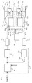
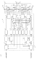
図1は、この発明の実施の形態1による電力変換装置を示す構成図であり、電力変換主回路1、ゲート駆動回路基板2a、2B、制御部3、および周辺部品の構成を図示している。図1に示すように、電力変換主回路1は、2レベルの電力変換回路として構成される。
FIG. 1 is a configuration diagram showing a power conversion device according to
この実施の形態1における電力変換主回路1は、電力変換主回路1の正極が直流母線5aに接続され、電力変換主回路1の負極が直流母線5bに接続される。電力変換主回路1は、正極側の直流母線5aに接続される第1のスイッチング部としてのスイッチング素子1aと、負極側の直流母線5bに接続される第2のスイッチング部としてのスイッチング素子1bと、スイッチング素子1aとスイッチング素子1bが直列に接続され、その電気的接続点5cに電力変換主回路1の出力端子4を備える。電力変換主回路1は、出力端子4から負荷(図示せず)に電力を供給する。第1のスイッチング部が導通すれば電力変換主回路1は直流母線5aの電位を出力端子4から負荷に供給する。第2のスイッチング部が導通すれば電力変換主回路1は直流母線5bの電位を出力端子4から負荷に供給する。このように2通りの電位を出力することから、2レベルの電力変換回路として機能する。
In power conversion
スイッチング素子1aは、トランジスタ素子10aとダイオード素子11aが並列に接続され、スイッチング素子1bは、トランジスタ素子10bとダイオード素子11bが並列に接続されている。なお、負荷の特性によっては、例えば抵抗負荷である場合にはダイオード素子11a、ダイオード素子11bの接続が省略されることがある。
The switching
なお、トランジスタ素子10a、10bは、図1ではMOSFETを図示しているが、特に限定するものではない。電気信号により低抵抗状態、高抵抗状態が切り替えられるデバイスであればよく、例えば、IGBT、バイポーラトランジスタといったデバイスを用いてもよい。スイッチング素子1a、1bの材料としては、広く用いられているSiの他に、SiC、GaN、ダイヤモンドなどのワイドバンドギャップ半導体を用いてもよい。
Although the
第1のゲート駆動部としてのゲート駆動回路2aは、スイッチング素子1aのゲート(G)−ソース(S)間に電圧印加できるように電気的に接続し、絶縁回路2gを介して入力された駆動信号に基づき、スイッチング素子1aにゲート電圧を印加する。同様に、第2のゲート駆動部としてのゲート駆動回路2bは、絶縁回路2hを介して入力された駆動信号に基づき、スイッチング素子1bにゲート電圧を印加する。
The
この発明の実施の形態1による電力変換装置では、図1に示すように、ゲート駆動回路2aとゲート駆動回路2bとの間にインピーダンス素子2eが設けられている。インピーダンス素子2eは、正極側の一端2e3がゲート駆動回路2aの接続端26aと接続されており、負極側の他端2e1がゲート駆動回路2bの接続端26bと接続されている。
In the power conversion device according to
検出部2fは、接続端26bと接続するインピーダンス素子2eの一端2e1と、中間部の接続点2e2とに接続し、インピーダンス素子2eの電圧を検出する。
The
出力端子4の電圧の変化に伴ってゲート駆動回路2aとゲート駆動回路2bの間の電圧が変化すると、インピーダンス素子2eの両端にかかる電圧が変化する。このインピーダンス素子2eの電圧を検出部2fが検出することにより、出力端子4の電位を検知できる。なお、図1では、検出部2fはインピーダンス素子2eの分圧を検出する例を示すが、検出部2fの入力耐圧が高ければ分圧は不要である。検出部2fをインピーダンス素子2eの両端に接続し、検出部2fはインピーダンス素子2eの両端にかかる電圧を検出する構成とすればよい。
When the voltage between the
図1に示す構成においては、検出部2fは絶縁回路を内蔵している。検出部2fは、絶縁回路を介して制御部3に接続され、検出部2fから制御部3に出力端子4の電位を表す出力電圧信号が入力される。なお、図1では矢印付きの線を信号線、矢印無しの線を電気的配線として図示している。
In the configuration shown in FIG. 1, the
制御部3は、補正回路としてのデッドタイム補正回路3a、第1の付加回路としてのデッドタイム付加回路3b、および第2の付加回路としてのデッドタイム付加回路3cにより構成される。デッドタイム補正回路3aは、電力変換主回路1の出力電圧指令値であるPWM信号を受け、検出部2fから検出された出力電圧信号に基づいて、デッドタイム補正を行う。
The
デッドタイム付加回路3bは、スイッチング素子1aの駆動信号に対してデッドタイムを付加してゲート駆動回路2aに駆動信号を出力する。デッドタイム付加回路3cは、反転論理部3dにより反転したスイッチング素子1bの駆動信号に対してデッドタイムを付加してゲート駆動回路2bに駆動信号を出力する。
The dead
次に、図2を参照して、出力端子4から出力される電圧の検出方法の詳細を示す。図2は、この発明の実施の形態1による電力変換装置の回路図であり、スイッチング素子1a、スイッチング素子1b、ゲート駆動回路2a、ゲート駆動回路2b、インピーダンス素子2e、および周辺の部品の回路を示す。
Next, with reference to FIG. 2, details of a method for detecting the voltage output from the
制御部3からのオン指令信号およびオフ指令信号は、制御信号絶縁部である絶縁回路2g、2hを介してゲート駆動回路2aおよびゲート駆動回路2bに伝わる。制御部3は、電力変換装置の通常動作中はゲート駆動回路2aおよびゲート駆動回路2bに対して、一方にオフ指令でもう一方にオン指令の信号を出すこともあれば、双方にオフ指令信号を出すことがある。制御部3は、電力変換装置の通常動作中はゲート駆動回路2aおよびゲート駆動回路2bに対して、双方にオン指令の信号を数十マイクロ秒以上出すことはない。
The on command signal and the off command signal from the
制御部3からのオン指令信号が、フォトカプラで構成される絶縁回路2g、2hに入力されるとフォトカプラの1次側の発光ダイオード20g、20hがそれぞれ点灯する。すると、フォトカプラの2次側のフォトトランジスタ21g、21hがそれぞれ導通状態になる。
When the ON command signal from the
ゲート駆動回路2aおよびゲート駆動回路2bの各部の電位が変化し、結局、ゲート駆動回路2aおよびゲート駆動回路2bのオン用トランジスタ20a1、20b1は導通状態に、オフ用トランジスタ20a2、20b2は非導通状態になる。
The potentials of the respective parts of the
オン用コンデンサ22a、22bに蓄えられた電荷は、それぞれオン用コンデンサ22a、22bの各正極から、それぞれオン用トランジスタ20a1、20b1、ゲート信号線23a、23b、スイッチング素子1a、1bの制御用ゲート端子12a、12b、制御用ソース端子13a、13b、ソース信号線24a、24b、オン用コンデンサ22a、22bの各負極への経路を通り、スイッチング素子1aおよびスイッチング素子1bに供給される。
The charges stored in the on-
スイッチング素子1aの制御用ゲート端子12aと制御用ソース端子13aの間、およびスイッチング素子1bの制御用ゲート端子12bと制御用ソース端子13bの間には正の電圧がかかり、スイッチング素子1aおよびスイッチング素子1bは導通状態になる。
A positive voltage is applied between the
一方、制御部3からのオフ指令信号が絶縁回路2g、2hに入力されると、フォトカプラの1次側の20g、20hがそれぞれ消灯する。すると、フォトカプラの2次側のフォトトランジスタ21g、21hがそれぞれ非導通状態になる。
On the other hand, when the off command signal from the
ゲート駆動回路2aおよびゲート駆動回路2bの各部の電位が変化し、結局、ゲート駆動回路2aおよびゲート駆動回路2bのオン用トランジスタ20a1、20b1が非導通状態に、オフ用トランジスタ20a2、20b2は導通状態になる。
The potentials of the respective parts of the
スイッチング素子1aおよびスイッチング素子1bの制御用ゲートに蓄えられた電荷は、それぞれゲート信号線23a、23b、ゲート抵抗25a1、25b1、オフ用トランジスタ20a2、20b2、ソース信号線24a、24b、制御用ソース端子13a、13bの各経路を通り、スイッチング素子1aおよびスイッチング素子1bから引き抜かれる。
Charges stored in the control gates of the
スイッチング素子1aの制御用ゲート端子12aと制御用ソース端子13aの間、およびスイッチング素子1bの制御用ゲート端子12bと制御用ソース端子13bの間は同電位となり、スイッチング素子1aおよびスイッチング素子1bは非導通状態になる。
The same potential is applied between the
このように、ゲート駆動回路2aおよびゲート駆動回路2bの構成から明らかなように、スイッチング素子1aおよびスイッチング素子1bの各ソース電位とゲート駆動回路2aおよびゲート駆動回路2bのオン用コンデンサ22a、22bの負極の電位はそれぞれ一致する。
Thus, as is apparent from the configurations of the
ここで、正極側のスイッチング素子1aのソース電位は、電力変換主回路1の出力電位に一致する。よって、ゲート駆動回路2aのオン用コンデンサ22aの負極の電位は、電力変換主回路1の出力の電位に一致する。負極側のスイッチング素子1bのソース電位は電力変換主回路1の負極の電位に一致する。よって、ゲート駆動回路2bのオン用コンデンサ22bの負極の電位は、電力変換主回路1の負極の電位に一致する。
Here, the source potential of the
また、ゲート駆動回路2aのオン用コンデンサの負極の電位は、ゲート駆動回路2aの接続端26aでの電位に一致する。ゲート駆動回路2bのオン用コンデンサ22bの負極の電位は、ゲート駆動回路2bの接続端26bでの電位と一致する。
Further, the potential of the negative electrode of the on-capacitor in the
インピーダンス素子2eは、ゲート駆動回路2aとゲート駆動回路2bとの間で電気的に接続されている。よって、インピーダンス素子2eの正極側の一端である2e3の電位は電力変換主回路1の出力電位に一致する。インピーダンス素子2eの負極側の一端である2e1の電位は電力変換主回路1の負極電位に一致する。検出部2fは、インピーダンス素子2eにかかる電圧を検出することで、電力変換主回路1の出力端子4から出力される電圧を電力変換主回路1の負極を基準電圧にして検出することができる。
The
負極電位を基準とした電力変換主回路の出力電圧値の一例としては、電気鉄道用途では750V、1500V、3000V程度、FA機器用途では300V、600Vである。車載用機器用途では48V〜750V程度まで様々である。いずれにせよインピーダンス素子2eにかかる電圧は電磁ノイズよりも十分に大きい。このように、信号レベルの低いゲート電圧の特徴を監視する方式のものとは異なり、本発明によれば検出部2fは誤動作することなく電力変換主回路の出力電圧を検出することができる。また、検出部2fからの信号に基づいて制御部により第1のゲート駆動部および第2のゲート駆動部を制御することで、誤動作することなくデッドタイムを補償することができる。
Examples of the output voltage value of the power conversion main circuit based on the negative electrode potential are about 750 V, 1500 V, and 3000 V for electric railway applications, and 300 V and 600 V for FA equipment applications. In vehicle equipment use, it is various from 48V to 750V. In any case, the voltage applied to the
以上のように、この発明の実施の形態1における電力変換装置では、寄生インダクタンスの削減や発生電力損失の冷却のために部品が複雑に入り組んでいる電力変換主回路や電力変換主回路周辺ではなく、ゲート駆動回路周辺に電力変換主回路の出力電位を検出するためのインピーダンス素子2eおよび検出部2fを設けるようにしたので、高度な技術を要することなく取り付け作業を行うことができる。このように、製造が容易でありながら、電力変換主回路の出力電圧を検出することができる。さらには、製造が容易でありながら、検出部2fからの信号に基づいて制御部により第1のゲート駆動部および第2のゲート駆動部を制御することでデッドタイムを補償することができる。
As described above, in the power conversion device according to the first embodiment of the present invention, not the power conversion main circuit or the vicinity of the power conversion main circuit in which components are complicatedly arranged for reducing the parasitic inductance and cooling the generated power loss. Since the
なお、この実施の形態1においては、図2に示すインピーダンス素子2eの接続点は、インピーダンス素子2eの負極側である一端2e1が、ゲート駆動回路2bの接続端26bに接続し、正極側である他端2e3は、ゲート駆動回路2aの接続端26aに接続するとした。接続端26bの電位はゲート駆動回路2bのオン用コンデンサ22bの負極の電位に一致し、接続端26aの電位はゲート駆動回路2aのオン用コンデンサ22aの負極の電位に一致するとしたが、これに限るものではない。
In the first embodiment, the connection point of the
接続端26aの電位がゲート駆動回路2aのオン用コンデンサ22aの正極の電位と一致するようにしてもよい。オン用コンデンサ22aの正極は、オン用コンデンサ22aの負極よりもオン用コンデンサ22aの充電電圧だけ高い電位にある。オン用コンデンサ22aの充電電圧は安定していることから好都合である。オン用コンデンサ22aの充電電圧は典型的には10Vから20Vの間にある。オン用コンデンサ22aの負極の電位は電力変換主回路1の出力の電位に一致することは先に述べた通りだが、接続端26aの電位はオン用コンデンサ22aの充電電圧だけ電力変換主回路1の出力の電位からずれることになる。インピーダンス素子2eにかかる電圧がオン用コンデンサ22aの充電電圧だけずれるものの、検出部2fがずれを考慮してインピーダンス素子2eの電圧を検出すれば本発明の効果を得られる。
You may make it the electric potential of the
同様に、接続端26aの電位がゲート駆動回路2aのゲート信号線23aの電位と一致するようにしてもよい。接続端26aの電位がゲート駆動回路2aのトランジスタ20a1、あるいはトランジスタ20a2の端子の電位と一致するようにしてもよい。このように、接続端26aの電位をゲート駆動回路2aの任意の電位と一致するようにしてもよい。いずれの場合も、接続端26aの電位は電力変換主回路1の出力の電位からずれることになる。インピーダンス素子2eにかかる電圧がずれるものの、検出部2fが電圧のずれを考慮してインピーダンス素子2eの電圧を検出すれば本発明の効果を得られる。
Similarly, the potential of the
負極電位を基準とした電力変換主回路の出力電圧が大きく、例えば300V以上の場合であれば、インピーダンス素子2eにかかる電圧がオン用コンデンサ22aの充電電圧だけずれるものの、ずれが小さいため、ずれを許容できる場合がある。この場合には検出部2fは特にずれを考慮することなく、インピーダンス素子2eの電圧を検出すればよい。
If the output voltage of the power conversion main circuit with respect to the negative electrode potential is large, for example, 300 V or more, the voltage applied to the
あるいは、電力変換主回路のスイッチング素子の電位状態(ON/OFF状態)を単に検出したい場合には、数百Vから数千Vの電位差に対して閾値を設定すればよく、数十V程度の誤差電圧の影響を考慮せずとも主回路であるスイッチング素子の電位状態(ON/OFF状態)を検出できる。電力変換主回路のスイッチング素子の電位状態(ON/OFF状態)を検出できればデッドタイム補償を行うことができる。 Alternatively, when simply detecting the potential state (ON / OFF state) of the switching element of the power conversion main circuit, a threshold value may be set for a potential difference of several hundred volts to several thousand volts, which is about several tens of volts. The potential state (ON / OFF state) of the switching element as the main circuit can be detected without considering the influence of the error voltage. If the potential state (ON / OFF state) of the switching element of the power conversion main circuit can be detected, dead time compensation can be performed.
なお、図2に示すように、ゲート駆動回路2aの中には、正極側のスイッチング素子1aのドレイン端子(IGBTであればコレクタ端子)と同電位の配線は存在しないが、ゲート駆動回路の構成によってはドレイン端子と同電位の配線が存在する場合がある。もし、接続端26aをドレイン端子と同電位の配線に設けると、接続端26aの電位と電力変換主回路1の出力の電位とのずれが大きくなってしまう。検出部2fが電位のずれを考慮してインピーダンス素子2eの電圧を検出することが困難となるため、避けることが望ましい。
As shown in FIG. 2, there is no wiring having the same potential as the drain terminal (collector terminal in the case of IGBT) of the positive-
接続端26bについても同様である。接続端26bの電位がゲート駆動回路2bのオン用コンデンサ22bの正極の電位と一致するようにしてもよい。接続端26aの電位をゲート駆動回路2bの任意の電位と一致するようにしてもよい。いずれの場合も、接続端26bの電位は電力変換主回路1の負極の電位からずれることになる。インピーダンス素子2eにかかる電圧がずれるものの、検出部2fが電圧のずれを考慮してインピーダンス素子2eの電圧を検出すれば本発明の効果を得られる。
The same applies to the
特に、トランジスタ素子に、SiC、GaN、ダイヤモンドといったSiと較べてバンドギャップが広い、いわゆるワイドバンドギャップ半導体材料を用い、高耐圧および高温動作が可能なスイッチング素子を用いて小型化を図る場合に、本発明は効果的である。電力変換主回路と電力変換主回路周辺の部品が複雑に入り組むが、本発明では、電力変換主回路の出力電位を検出するためのインピーダンス素子2eおよび検出部2fをゲート駆動回路周辺に設けるようにしたので、高度な技術を要することなく取り付け作業を行うことができる。このように、製造が容易でありながあら電力変換主回路の出力電圧を検出することができる。さらには、製造が容易でありながら、検出部2fからの信号に基づいて制御部により第1のゲート駆動部および第2のゲート駆動部を制御することでデッドタイムを補償することができる。
In particular, when a transistor element is made of a wide bandgap semiconductor material having a wider bandgap than Si such as SiC, GaN, and diamond, and a switching element capable of high withstand voltage and high temperature operation is used for miniaturization, The present invention is effective. The power conversion main circuit and components around the power conversion main circuit are complicated, but in the present invention, the
この実施の形態1において、インピーダンス素子2eは、図2に示すように、2以上直列接続した抵抗20e1、20e2、・・20enにより構成される。制御部3の電位がゲート駆動回路2aよりもゲート駆動回路2bの電位に近い場合は、2以上直列接続した抵抗20e1、20e2、・・20enのうち、一端がゲート駆動回路2bの接続端26bに接続されている抵抗20e1の両端2e1、2e2に、検出部2fを接続することが望ましい。
In the first embodiment, as shown in FIG. 2, the
なお、制御部3の電位がゲート駆動回路2bよりもゲート駆動回路2aの電位に近い場合は、2以上直列接続した抵抗20e1、20e2、・・20enのうち、一端がゲート駆動回路2aの接続端26aに接続されている抵抗20enの両端に、検出部2fが接続することが望ましい。
When the potential of the
このように、制御部3とゲート駆動回路2aとゲート駆動回路2bの電位の関係に応じて検出部2fが接続される抵抗20e1(または抵抗20en)を変更することで、検出部fに絶縁耐圧の低いフォトカプラを用いることができ、絶縁回路としても機能する。
In this way, by changing the resistor 20e1 (or the resistor 20en) to which the
このようなインピーダンス素子2eと検出部2fの構成においては、出力端子4の電位が高電位状態にある場合、インピーダンス素子2eの両端には高電圧がかかり、フォトカプラからなる検出部2fが接続された抵抗20e1(または抵抗20en)には、分圧された電圧がかかる。フォトカプラからなる検出部2fの絶縁電圧に応じてインピーダンス素子2eを構成する抵抗20e1、20e2、・・20enの直列数を調整することが望ましい。
In such a configuration of the
フォトカプラからなる検出部(絶縁回路)2fにおいては、1次側は発光ダイオード20fで構成されており、インピーダンス素子2eの端部の抵抗20e1(または抵抗20en)に接続されている。
In the detection unit (insulation circuit) 2f made of a photocoupler, the primary side is constituted by a light emitting diode 20f, and is connected to the resistor 20e1 (or resistor 20en) at the end of the
検出部2fとしてのフォトカプラの1次側に電圧がかかると、フォトカプラの1次側である発光ダイオード20fが点灯し、フォトカプラの2次側であるフォトトランジスタ21fが導通状態となる。
When a voltage is applied to the primary side of the photocoupler as the
フォトカプラの2次側であるフォトトランジスタ21fが導通状態になったことにより、制御部3は、電力変換主回路の負極の電位を基準にして出力端子4の電位が高電位状態にあることを検知する。
As the phototransistor 21f, which is the secondary side of the photocoupler, becomes conductive, the
一方、電力変換主回路の負極の電位を基準にして出力端子4の電位が低くなり電位が零になった場合、インピーダンス素子2eの両端には電圧がかからないため、フォトカプラからなる検出部2fが接続された抵抗にも電圧がかからない。
On the other hand, when the potential of the
検出部2fとしてのフォトカプラの1次側に電圧がかからないことから、フォトカプラの2次側である発光ダイオード20fが消灯し、フォトカプラの2次側であるフォトトランジスタ21fが非導通状態となる。
Since no voltage is applied to the primary side of the photocoupler as the
フォトカプラの2次側であるフォトトランジスタ21fが非導通状態になったことにより、制御部3は、電力変換主回路の負極の電位を基準にして出力端子4の電位が零であることを検知する。
When the phototransistor 21f, which is the secondary side of the photocoupler, becomes non-conductive, the
上述のように、この発明の実施の形態1では、インピーダンス素子2eを2以上直列接続した抵抗(20e1、20e2、・・20en)により電圧を分圧することで、出力電圧を検知できるだけでなく、検出部としてフォトカプラを用いることにより、絶縁回路として制御部を保護できる。なお、この発明の実施の形態1では、検出部2fはインピーダンス素子2eの分圧を検出する例を示したが、検出部2fの入力耐圧が高ければ分圧は不要である。検出部2fをインピーダンス素子2eの両端に接続し、検出部2fはインピーダンス素子2eの両端にかかる電圧を検出する構成とすればよい。この場合には、インピーダンス素子2eを2以上直列接続した抵抗で構成してもよいが1個の抵抗で構成することもできる。
As described above, in the first embodiment of the present invention, not only the output voltage can be detected but also detected by dividing the voltage by the resistors (20e1, 20e2,... 20en) in which two or
さらに、従来技術のように出力端子と直流母線の低圧側との間にセンサーを設ける場合は、ゲート駆動回路の電源とは別にセンサーの電源が必要であるのに対し、上記構成では検出部の電源をゲート駆動回路の電源より得ることができ、さらに小型かつ簡素な電力変換装置を得ることができる。 Furthermore, when a sensor is provided between the output terminal and the low voltage side of the DC bus as in the prior art, a sensor power supply is required separately from the power supply of the gate drive circuit. The power source can be obtained from the power source of the gate drive circuit, and a smaller and simpler power converter can be obtained.
上記においては、検出部2fがインピーダンス素子2eの電圧を検出する構成にて説明したが、検出部がインピーダンス素子に通流する電流を検出する構成としてもよい。図3を用いて説明する。
In the above description, the
図3の構成では、検出部2fであるフォトカプラの1次側が、ゲート駆動回路2aの接続端26aに一端を接続するインピーダンス素子2eの他端と、ゲート駆動回路2bの接続端26bとの間に、直列で挿入されている。図3ではインピーダンス素子2eは1個の抵抗で構成されているが、2以上直列接続した抵抗で構成してもよい。その他の構成は図2と同様であり、その詳細な説明は省略する。
In the configuration of FIG. 3, the primary side of the photocoupler that is the
電力変換主回路の負極の電位を基準にして出力端子4の電位が高電位状態にある場合、インピーダンス素子2eの両端には高電圧がかかり、よって電流が通流する。フォトカプラの1次側に電流が通流するため、1次側の発光ダイオード20fが点灯し、フォトカプラの2次側のフォトトランジスタ21fが導通状態となり、制御部3は、出力端子4の電位が高電位状態にあることを検知する。
When the potential of the
一方、電力変換主回路の負極の電位を基準にして出力端子4の電位が低くなり零になった場合、インピーダンス素子2eの両端には電圧がかからないため、よって電流が通流しない。フォトカプラの1次側に電流が通流しないため、1次側の発光ダイオード20fが消灯し、フォトカプラ2次側のフォトトランジスタ21fが非導通状態となり、制御部3は、出力端子4の電位が零であることを検知する。
On the other hand, when the potential of the
このように、検出部がインピーダンス素子に通流する電流を検出する構成であっても、検出部2fがインピーダンス素子2eの電圧を検出する構成と同様の効果を得ることができる。
Thus, even if the detection unit is configured to detect the current flowing through the impedance element, the same effect as the configuration in which the
なお、検出部2fではフォトカプラを用いたが、フォトカプラ以外にもホール素子を用いてインピーダンス素子に流れる電流を検出する構成としてもよい。また、シャント抵抗を用いてインピーダンス素子に流れる電流を検出する構成としてもよい。いずれにおいても、フォトカプラを用いた場合と同様の効果を得ることができる。
Although the photocoupler is used in the
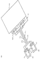
図4は、この発明の実施の形態1による電力変換装置の配置図であり、スイッチング素子1aからなるモジュール100、スイッチング素子1bからなるモジュール101、ゲート駆動回路2a、ゲート駆動回路2b、インピーダンス素子2e、および周辺の部品の配置を示す。
FIG. 4 is a layout diagram of the power conversion device according to the first embodiment of the present invention. The
図4に示すように、スイッチング素子1aおよびスイッチング素子1bは、それぞれ1つの筐体に納められた、いわゆる1in1モジュールとなっている。モジュールは1個のスイッチング半導体チップ、または2個以上のスイッチング半導体チップを内蔵している。スイッチング素子1aからなるモジュール100とスイッチング素子1bからなるモジュール101は、ブスバー110にとりつけられており、電力変換主回路1を構成している。なお、図4では、スイッチング素子を1個のモジュールにより構成したが、これに限るものではない。2個以上のモジュールを電気的に並列接続することによりスイッチング素子を構成してもよい。
As shown in FIG. 4, each of the
ゲート駆動回路2aおよびゲート駆動回路2bは、それぞれ1枚のゲート駆動回路基板2a、2Bに配設されている。モジュール100およびモジュール101は、それぞれゲート駆動回路2a、ゲート駆動回路2bとゲート信号線23a、23b、ソース信号線24a、24bで結ばれている。
The
つまり、スイッチング素子1aからなるモジュール100は、ゲート駆動回路2aのゲート・ソース間電圧がそれぞれゲート信号線23a、ソース信号線24aで接続され、伝達される。同様に、スイッチング素子1bからなるモジュール101は、ゲート駆動回路2bのゲート・ソース間電圧がそれぞれゲート信号線23b、ソース信号線24bで接続され、伝達される。
That is, in the
従来より、スイッチング素子のスイッチング動作に伴って、スイッチング素子の周辺は電磁ノイズが大きいことが知られている。電磁ノイズにより、ゲート信号線、ソース信号線の伝達信号が変形し、スイッチング素子が誤動作する恐れがある。 2. Description of the Related Art Conventionally, it is known that electromagnetic noise is large around a switching element in accordance with the switching operation of the switching element. Due to the electromagnetic noise, the transmission signal of the gate signal line and the source signal line may be deformed and the switching element may malfunction.
これに対しては、ゲート信号線、ソース信号線を隣接して配置し、ゲート信号線とソース信号線が作るループを小さくすることが行われている。電磁ノイズの影響を抑え、ゲート駆動回路のゲート・ソース間電圧が変形することなくスイッチング素子のゲート・ソース間に伝達される。 For this, a gate signal line and a source signal line are arranged adjacent to each other, and a loop formed by the gate signal line and the source signal line is reduced. The influence of electromagnetic noise is suppressed, and the gate-source voltage of the gate drive circuit is transmitted between the gate and source of the switching element without deformation.
図4の構成においても、ゲート信号線23aとソース信号線24a、およびゲート信号線23bとソース信号線24bは、隣接して配置されている。図4の構成の特徴は、ソース信号線24aとソース信号線24bも隣接して配置されていることである。すなわち、ソース信号線24aとソース信号線24bとの距離は、ゲート信号線23aとソース信号線24aとの距離およびゲート信号線23bとソース信号線24bとの距離のいずれかと同じかそれ未満である。このように、ソース信号線24aとソース信号線24bが作るループを小さくしていることである。
Also in the configuration of FIG. 4, the
この構成により、電磁ノイズの影響を抑え、出力端子の電位が変形することなくインピーダンス素子に伝達される。制御部は出力端子の電位を精度よく検知できる。 With this configuration, the influence of electromagnetic noise is suppressed, and the potential of the output terminal is transmitted to the impedance element without being deformed. The control unit can accurately detect the potential of the output terminal.
図4の構成においては、インピーダンス素子2eは、ゲート駆動回路2aとゲート駆動回路2bとの間の空間において配線して接続している。インピーダンス素子2eは、ゲート駆動回路2aとゲート駆動回路2bとの空間絶縁距離を考慮して配置すればよい。
In the configuration of FIG. 4, the
一般に、絶縁を確保するにあたっては、空間絶縁距離の方が沿面絶縁距離よりも短くて済む。図4の構成によれば、インピーダンス素子の配線長を短く抑えることができる。 Generally, in order to ensure insulation, the space insulation distance may be shorter than the creeping insulation distance. According to the configuration of FIG. 4, the wiring length of the impedance element can be kept short.
図5は、この発明の実施の形態1による電力変換装置の他の配置例を示す図である。図5の構成では、スイッチング素子1aとスイッチング素子1bが1枚のゲート駆動回路基板2で構成されている。インピーダンス素子2eは、ゲート駆動回路基板2の上に設置されており、回路パターンにより結線されている。
FIG. 5 is a diagram showing another example of arrangement of the power conversion device according to
この構成であれば、ゲート駆動回路基板の製造段階でインピーダンス素子の取り付け作業を完了することができる。インピーダンス素子の取り付け工程を別に設ける必要がないため、低コスト化を図ることができる。さらに、この構成においても、デッドタイムを補償することができる。 With this configuration, the mounting operation of the impedance element can be completed at the stage of manufacturing the gate drive circuit board. Since it is not necessary to provide a separate process for attaching the impedance element, the cost can be reduced. In addition, this configuration can also compensate for dead time.
実施の形態2.
実施の形態1では、検出部2fにフォトカプラを用いて絶縁回路と兼用したが、実施の形態2では、絶縁回路と検出部は別とし、検出部としてコンパレータを用いた場合について説明する。
In the first embodiment, the
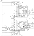
図6は、この発明の実施の形態2による電力変換装置を示す構成図であり、電力変換主回路1、ゲート駆動回路基板2、制御部3、および周辺部品の構成を図示している。なお、図6では矢印付きの線を信号線、矢印無しの線を電気的配線として図示している。
FIG. 6 is a block diagram showing a power conversion device according to
図6に示すように、ゲート駆動回路2aとゲート駆動回路2bとの間にインピーダンス素子2eが設けられている。インピーダンス素子2eは、正極側の一端2e3がゲート駆動回路2aの接続端26aと接続されており、負極側の他端2e1がゲート駆動回路2bの接続端26bと接続されている。インピーダンス素子2eには、電圧を検出する検出部2fとしてコンパレータが接続されている。コンパレータからなる検出部2fにより検出した出力電圧信号を、絶縁回路2iを介して制御部3のデッドタイム補正回路3aに出力し、また、反転論理部2kにより反転した反転出力電圧信号も、絶縁回路2jを介してデッドタイム補正回路3aに出力するように構成されている。
As shown in FIG. 6, an
図7は、この発明の実施の形態2による電力変換装置の回路図であり、スイッチング素子1a、スイッチング素子1b、ゲート駆動回路2a、ゲート駆動回路2b、インピーダンス素子2e、および周辺の部品の回路を示す。
FIG. 7 is a circuit diagram of a power conversion device according to
図7に示すように、ゲート駆動回路2aおよびゲート駆動回路2bには、それぞれオン用コンデンサ22a、22bとオフ用コンデンサ27a、27bがあり、オン用コンデンサ22a、22bの負極とオフ用コンデンサ27a、27bの正極が直列接続されている。オン用コンデンサ22a、22bとオフ用コンデンサ27a、27bの接続点は、それぞれソース信号線24a、24bを介して、スイッチング素子1aおよびスイッチング素子1bの各制御用ソース端子13a、13bに接続されている。
As shown in FIG. 7, the
その他の構成については図1および図2と同様であり、その説明を省略する。結局、ゲート駆動回路2aの接続端26aの電位はオン用コンデンサ22aの負極の電位に一致し、さらには電力変換主回路1の出力の電位に一致する。ゲート駆動回路2bの接続端26bの電位はオン用コンデンサ22bの負極の電位に一致し、さらには電力変換主回路1の負極の電位に一致する。
Other configurations are the same as those in FIGS. 1 and 2, and the description thereof is omitted. Eventually, the potential of the
次に、電力変換主回路の出力端子4から出力される電圧の検出方法の詳細について、図7を用いて説明する。図7に示すように、制御部3からのオン指令信号は、制御信号絶縁部である絶縁回路2g、2hを介してゲート駆動回路2aおよびゲート駆動回路2bに伝わる。絶縁回路2g、2hは、フォトカプラ部品により構成される。
Next, details of a method for detecting the voltage output from the
制御部3からのオン指令信号が、絶縁回路2g、2hに入力されるとフォトカプラの1次側の発光ダイオード20g、20hがそれぞれ点灯する。すると、フォトカプラの2次側のフォトトランジスタ21g、21hがそれぞれ導通状態になる。
When the ON command signal from the
ゲート駆動回路2aおよびゲート駆動回路2bの各部の電位が変化し、結局、ゲート駆動回路2aおよびゲート駆動回路2bのオン用トランジスタ20a1、20b1は導通状態に、オフ用トランジスタ20a2、20b2は非導通状態になる。
The potentials of the respective parts of the
オン用コンデンサ22a、22bに蓄えられた電荷は、それぞれオン用コンデンサ22a、22bの各正極から、それぞれオン用トランジスタ20a1、20b1、ゲート信号線23a、23b、スイッチング素子1a、1bの制御用ゲート端子12a、12b、制御用ソース端子13a、13b、ソース信号線24a、24b、オン用コンデンサ22a、22bの各負極への経路を通り、スイッチング素子1aおよびスイッチング素子1bに供給される。
The charges stored in the on-
スイッチング素子1aおよびスイッチング素子1bの制御用ゲート端子12a、12bと制御用ソース端子13a、13bには正の電圧がかかり、スイッチング素子1aおよびスイッチング素子1bは導通状態になる。
A positive voltage is applied to the
一方、制御部3からのオフ指令信号が絶縁回路2g、2hに入力されると、フォトカプラの1次側の発光ダイオード20g、20hがそれぞれ消灯する。すると、フォトカプラの2次側のフォトトランジスタ21g、21hがそれぞれ非導通状態になる。
On the other hand, when the OFF command signal from the
ゲート駆動回路2aおよびゲート駆動回路2bの各部の電位が変化し、結局、ゲート駆動回路2aおよびゲート駆動回路2bのオン用トランジスタ20a1、20b1が非導通状態に、オフ用トランジスタ20a2、20b2は導通状態になる。
The potentials of the respective parts of the
オフ用コンデンサ27a、27bに蓄えられた電荷が、オフ用コンデンサ27a、27bの各正極から、ソース信号線24a、24b、スイッチング素子1a、1bの制御用ソース端子13a、13b、スイッチング素子1a、1bの制御用ゲート端子12a、12b、ゲート信号線23a、23b、オフ用トランジスタ20a2、20b2、オフ用コンデンサ27a、27bの各負極への経路を通り、スイッチング素子1aおよびスイッチング素子1bにそれぞれ供給される。
The charges stored in the
スイッチング素子1aおよびスイッチング素子1bの制御用ゲート端子12a、12bと制御用ソース端子13a、13bには、それぞれ負の電圧がかかり、スイッチング素子1aおよびスイッチング素子1bは非導通状態となる。
Negative voltages are applied to the
このように、ゲート駆動回路2aおよびゲート駆動回路2bの構成から明らかなように、スイッチング素子1aおよびスイッチング素子1bの各ソース電位とゲート駆動回路2aおよびゲート駆動回路2bのオン用コンデンサ22a、22bの負極の電位はそれぞれ一致する。
Thus, as is apparent from the configurations of the
ここで、正極側のスイッチング素子1aのソース電位は、電力変換主回路1の出力電位に一致する。よって、ゲート駆動回路2aのオン用コンデンサ22aの負極の電位は、電力変換主回路1の出力の電位に一致する。負極側のスイッチング素子1bのソース電位は、電力変換主回路1の負極電位に一致する。よって、ゲート駆動回路2bのオン用コンデンサ22bの負極の電位は、電力変換主回路1の負極電位に一致する。
Here, the source potential of the
また、ゲート駆動回路2aのオン用コンデンサの負極の電位は、ゲート駆動回路2aの接続端26aでの電位に一致する。ゲート駆動回路2bのオン用コンデンサ22bの負極の電位は、ゲート駆動回路2bの接続端26bでの電位と一致する。
Further, the potential of the negative electrode of the on-capacitor in the
ゲート駆動回路2aとゲート駆動回路2bとの間にインピーダンス素子2eが設けられている。インピーダンス素子2eは、正極側の一端2e3がゲート駆動回路2aの接続端26aと接続されており、負極側の他端2e1がゲート駆動回路2bの接続端26bと接続されている。検出部2fは、インピーダンス素子2eでの電圧を検出することで、電力変換主回路1の出力端子4から出力される電圧を検出することができる。
An
実施の形態2においては、図7に示すように、検出部2fはコンパレータにより構成される。インピーダンス素子2eは、2以上直列接続した抵抗(20e1、20e2、・・20en)により構成される。検出部2fの入力電圧仕様に応じてインピーダンス素子2eを構成する抵抗20e1、20e2、・・20enの直列数を調整することが望ましい。なお、図7では、検出部2fはインピーダンス素子2eの分圧を検出する例を示すが、検出部2fの入力耐圧が高ければ分圧は不要である。検出部2fをインピーダンス素子2eの両端に接続し、検出部2fはインピーダンス素子2eの両端にかかる電圧を検出する構成とすればよい。この場合には、インピーダンス素子2eを2以上直列接続した抵抗で構成してもよいが1個の抵抗で構成することもできる。
In the second embodiment, as shown in FIG. 7, the
制御部3の電位がゲート駆動回路2aよりもゲート駆動回路2bの電位に近い場合、ゲート駆動回路2bの接続端26bに2以上直列接続したインピーダンス素子2eの一端、つまり、抵抗20e1の一端が接続され、抵抗20e1の他端に、検出部2fであるコンパレータの一方の入力端2f1に接続される。
When the potential of the
本実施例では検出部2fであるコンパレータの電源はゲート駆動回路2bの電源より得ている。オン用コンデンサ22b、オフ用コンデンサ27bを用いることにより両極電源を得ることができる。従来技術のように出力端子と直流母線の低圧側との間にセンサーを設ける場合は、ゲート駆動回路の電源とは別にセンサーの電源が必要であるのに対し、上記構成では検出部の電源をゲート駆動回路の電源より得ることができ、さらに小型かつ簡素な電力変換装置を得ることができる。
In this embodiment, the power source of the comparator which is the
検出部2fであるコンパレータの他方の入力端2f2には、ドライバ電源を抵抗分圧して得られる基準電圧が入力される。出力端子4の電位が高電位状態にある場合、インピーダンス素子2eの両端には高電圧がかかり、コンパレータが接続されている抵抗20e1にも分圧された電圧がかかる。コンパレータの他端の基準電圧を越えるのでコンパレータの出力はhigh状態となる。一方、出力端子4の電位が低くなり電位差が零になった場合、インピーダンス素子2eの両端には電圧がかからないため、コンパレータが接続された抵抗にも電圧がかからない。コンパレータの他端の基準電圧を越えないのでコンパレータの出力はlow状態となる。
A reference voltage obtained by resistance-dividing the driver power supply is input to the other input terminal 2f2 of the comparator which is the
一般に、コンパレータの入力端子は入力インピーダンスが高く、感度が高い。本実施の形態のように検出部2fとしてコンパレータを用いれば、インピーダンス素子2eを構成する抵抗の抵抗値を大きくしても検出部2fはインピーダンス素子2eの電圧を感度良く検出することができる。インピーダンス素子2eの通流電流を少なくすることができ、インピーダンス素子2eの発熱を抑えることができる。
In general, an input terminal of a comparator has high input impedance and high sensitivity. If a comparator is used as the
さらに、本実施の形態であれば、電力変換装置の動作時についてコンパレータの入力端子の入力電圧範囲をコンパレータの両極電源電圧値よりも内側に収めることができる。コンパレータの入力端子の入力電圧がコンパレータの両極電源電圧値に一致すると、コンパレータの内部回路が飽和し、コンパレータ動作が遅くなることがある。コンパレータの入力端子の入力電圧がコンパレータの両極電源電圧よりも外側にあると、コンパレータの内部回路の絶縁が劣化し、コンパレータが破壊することがある。本実施の形態であれば、コンパレータ動作が遅くなることはなく、コンパレータが破壊することはない。 Further, according to the present embodiment, the input voltage range of the input terminal of the comparator can be kept inside the bipolar power supply voltage value of the comparator during the operation of the power conversion device. When the input voltage at the input terminal of the comparator matches the bipolar power supply voltage value of the comparator, the internal circuit of the comparator may be saturated and the comparator operation may be delayed. If the input voltage at the input terminal of the comparator is outside the bipolar power supply voltage of the comparator, the insulation of the internal circuit of the comparator may deteriorate and the comparator may be destroyed. In the present embodiment, the comparator operation is not delayed and the comparator is not destroyed.
なお、この実施の形態2では、インピーダンス素子2eを2以上直列接続した抵抗または1個の抵抗により構成することができるとして説明したが、特に限定するものではない。インピーダンス素子2eを2以上直列接続したコンデンサまたは1個のコンデンサにより構成した場合でも、同様の効果を得られる。さらに、インピーダンス素子2eを2以上直列接続したダイオードまたは1個のダイオードにより構成した場合でも、同様の効果を得られる。
Although the second embodiment has been described on the assumption that two or
また、この実施の形態2では、検出部2fがインピーダンス素子2eの電圧を検出する構成にて説明したが、特に限定するものではない。検出部2fがインピーダンス素子に通流する電流を検出する構成とした場合においても、同様の効果を得られる。
In the second embodiment, the
なお、検出部2fであるコンパレータの他方の入力端2f2に入力される基準電圧の電圧値は、直流母線の電位に応じて適切に調整しておく必要がある。通常、電力変換装置に電力を供給する直流母線の電位は安定しており、前記基準電圧の電圧値の調整は一度行えば良い。本実施の形態では、ドライバ電源を抵抗分圧して調整することにより基準電圧を得ている。しかしながら、特殊な用途の電力変換装置においては、直流母線の通常時の電位が大きく変動することがある。この場合には検出部2fの閾値を生成する前記基準電圧の電圧値は、直流母線の電位によって可変となるように構成することが望ましい。
Note that the voltage value of the reference voltage input to the other input terminal 2f2 of the comparator, which is the
上記の変形例として、図8に示すように、直流母線5aとゲート駆動回路2b中のオフ用コンデンサ27bの負極側の接続端とを抵抗23b7と23b8で電気的に接続し、その分圧電位を利用する電力変換装置がある。この分圧電位を前記基準電圧の電圧値として用いる。これにより、直流母線5aの通常時の電位が変動しても、それに応じて閾値電圧が変動するため検出部2fの誤検知、誤動作を防止できる。さらに、本構成であれば、落雷などで母線電圧が異常に変動して瞬時低下又は瞬時上昇した場合であっても、検出部2fの誤検知、誤動作を防止できる。
As a modification of the above, as shown in FIG. 8, the
本実施の形態では図8に示すように、ゲート駆動回路2aの中には、正極側のスイッチング素子1aのドレイン端子(IGBTであればコレクタ端子)と同電位の配線は存在しないが、ゲート駆動回路の構成によっては存在する場合がある。上記図8の変形例として述べる。この場合、ゲート駆動回路2a上にある正極側のスイッチング素子1aのドレイン端子(IGBTであればコレクタ端子)と同電位の配線の電位は直流母線5aとも同電位である。したがって、上記ゲート駆動回路2a上にある同電位の配線とゲート駆動回路2b中のオフ用コンデンサ27bの負極側の接続端とを抵抗23b7と23b8で電気的に接続することで、図8と同様の効果を得ることができる。さらなる効果として、直流母線5aからの電気的な接続線を配線する必要が無く、装置の構成が容易になる。
In the present embodiment, as shown in FIG. 8, the
次に、デッドタイム補正方法について説明する。
一般に、デッドタイムは、スイッチング素子や、そのゲート駆動回路の遅延時間等を考慮して、電力変換主回路の出力端子でのデッドタイムは、下記の式(1)を満たすようスイッチング信号を出力する制御部のデッドタイム付加回路により、予め設定される。
Next, the dead time correction method will be described.
In general, the dead time considers the switching element and the delay time of its gate drive circuit, etc., and the dead time at the output terminal of the power conversion main circuit outputs a switching signal so as to satisfy the following equation (1). It is preset by the dead time addition circuit of the control unit.
Tdead+ = Tdead + Td-on − Td-off > 0 ・・・(1) Tdead + = Tdead + Td-on-Td-off> 0 (1)
ここで、
Tdead :制御部にて生成されるデッドタイム
Tdead+ :電力変換主回路1の出力端子4でのデッドタイム
Td-on :オン遅延時間
Td-off :オフ遅延時間
(Td-on、Td-offには、信号の上昇時間Tr や下降時間Tf を含む)
here,
Tdead: Dead time generated by the control unit Tdead + : Dead time at the
また、制御部から出力されたスイッチング信号は、高電圧部から低電圧部へのノイズを防止する目的や、絶縁破壊に対する安全性を確保するために、絶縁回路であるフォトカプラを介してゲート駆動回路に供給される。 The switching signal output from the control unit is driven by a gate via a photocoupler, which is an insulation circuit, to prevent noise from the high-voltage part to the low-voltage part and to ensure safety against dielectric breakdown. Supplied to the circuit.
フォトカプラは、入力電流により発光ダイオードが発光し、この光をフォトトランジスタで出力電流に変換している。しかしフォトトランジスタのベースキャリアのライフタイムの影響と、コレクタからベースへ負帰還がかかるミラー積分効果により、フォトトランジスタがオフからオンに変化するために要するオン遅延時間よりも、オンからオフに変化するために要するオフ遅延時間の方が大幅に長くなる。 In the photocoupler, a light emitting diode emits light by an input current, and this light is converted into an output current by a phototransistor. However, because of the influence of the lifetime of the base carrier of the phototransistor and the Miller integration effect that negative feedback from the collector to the base changes from the on delay time required for the phototransistor to change from off to on, it changes from on to off. The off-delay time required for is significantly longer.
このことは、ルネサスエレクトロニクス株式会社のホームページに「汎用フォトカプラの応答速度」(URL:http://japan.renesas.com/products/opto/technology/speed/index.jsp)として記載されているとおりである。 This is as described on the Renesas Electronics Corporation website as "Response speed of general-purpose photocouplers" (URL: http://japan.renesas.com/products/opto/technology/speed/index.jsp) It is.
従って、フォトトランジスタ分の遅延時間が Td-on − Td-off < 0 であるため、式(1)において、Tdead+として正の値を確保するためには、デッドタイムTdeadとして大きな値を設ける必要があった。 Therefore, since the delay time for the phototransistor is Td-on-Td-off <0, in order to secure a positive value as Tdead + in Equation (1), it is necessary to provide a large value as the dead time Tdead. was there.
さらに、上述のような遅れ要素は負荷電流や温度条件などさまざまな要因により一定の遅れ要素ではなく、実際に補正すべきデッドタイムであるTdead+は上述のような変動要因により一定値ではないことが知られている。 Furthermore, the delay element as described above is not a constant delay element due to various factors such as load current and temperature conditions, and Tdead + which is a dead time to be actually corrected is not a constant value due to the above-described fluctuation factors. It has been known.
従来技術のような出力端子の電位を検出してデッドタイム補正に用いる方法では、上述のような遅れ要素があっても、出力端子の電位を直接検出することで電力変換主回路の出力端子でのデッドタイムTdead+を正確に知ることができるので、精度よくデッドタイム補正を実施することができる。 In the method of detecting the potential of the output terminal and using it for dead time correction as in the prior art, the output terminal of the power conversion main circuit is detected directly by detecting the potential of the output terminal even if there is a delay element as described above. Since the dead time Tdead + can be accurately known, the dead time can be corrected accurately.
しかしながら、従来技術では示されていないが、実際に従来技術を実施する場合には、センサーの信号とカウンタの間にはフォトカプラのような絶縁回路が必要となる。この理由は上述と同様の理由である。 However, although not shown in the prior art, when the prior art is actually implemented, an insulation circuit such as a photocoupler is required between the sensor signal and the counter. The reason is the same as described above.
特別な例として、電力変換主回路の低圧側に接続された直流母線の低圧側の電位と制御器のグランド(接地電位)が同電位であり、ノイズ等の問題がない場合には、センサーの信号とカウンタ間の絶縁回路は省略しても問題ない場合もあるが、ほとんどの場合は、絶縁回路を介して信号を授受するのが一般的である。 As a special example, if the potential on the low-voltage side of the DC bus connected to the low-voltage side of the power conversion main circuit and the controller ground (ground potential) are the same potential and there is no problem such as noise, Although there may be no problem even if the insulation circuit between the signal and the counter is omitted, in most cases, the signal is generally transmitted and received through the insulation circuit.
したがって、従来技術ではフォトカプラのような絶縁回路の遅れ要素により、カウンタが検出したデッドタイムは絶縁回路のON遅延時間−OFF遅延時間だけ誤差を持つことになる。 Therefore, in the prior art, due to the delay element of the insulation circuit such as a photocoupler, the dead time detected by the counter has an error corresponding to the ON delay time-OFF delay time of the insulation circuit.
この発明の実施の形態2による電力変換装置では、検出部2fにより検出された出力電圧信号は、絶縁回路2iを介して制御部3に出力し、また、反転論理部2kにより反転した反転出力電圧信号も、絶縁回路2jを介して制御部3に出力するように構成している。
In the power conversion device according to
図9に、絶縁回路2i、2jのタイムチャートを示す。通常の絶縁回路2iの検出パルス時間Tout+は、式(2)で求まり、反転論理部2kを介した絶縁回路2jの検出パルス時間Tout++は、式(3)で求まる。したがって、出力端子4の電位検出パルス時間Toutは、式(4)で正確に求めることができる。
FIG. 9 shows a time chart of the insulating
Tout+ = Tout − Ton + Toff ・・・(2)
Tout++ = Tout − Toff + Ton ・・・(3)
Tout = ( Tout++ Tout++ ) / 2 ・・・(4)
Tout + = Tout-Ton + Toff (2)
Tout ++ = Tout−Toff + Ton (3)
Tout = (Tout + + Tout ++ ) / 2 ··· (4)
ここで、
Tout :出力端子4の電位検出パルス時間
Tout+ :通常の絶縁回路2iの検出パルス時間
Tout++ :反転論理部2kを介する絶縁回路2jの検出パルス時間
Ton :絶縁回路のオン遅延時間
Toff :絶縁回路のオフ遅延時間
here,
Tout: potential detection pulse time Tout + of the output terminal 4: detection pulse time Tout ++ of the
したがって、式(4)で求めた出力端子4の電位検出パルス時間を用いてデッドタイム補正を実施することで、従来技術に比べてデッドタイム補正の精度を向上することができる。ここで、2個のフォトカプラである絶縁回路2i、2jは近接して配置することが望ましい。電気的条件、温度条件が揃うことからフォトカプラの遅れ時間が揃う効果が得られる。
Therefore, by performing the dead time correction using the potential detection pulse time of the
なお、絶縁回路2i、2jの遅れが十分無視できる時間であれば、反転論理部は省略してもよい。一般に、高性能な絶縁回路ほど上記信号伝達遅れ時間が短くなるが、高価になる。反転論理部を用いることで、安価な絶縁回路であっても高精度に出力端子の電位検出パルス時間Toutを検出でき、コスト低減にも繋がる。
Note that the inversion logic unit may be omitted as long as the delay of the insulating
図10に、デッドタイム補正回路3aのブロック図を示す。デッドタイム補正回路3aでは、式(4)に基づき出力端子4の電位検出パルス時間Toutをカウントし、補正信号のカウント値Tvref+との差分から誤差電圧である電力変換主回路1の出力端子4でのデッドタイムTdead+をTvref+-Toutから算出する。このTdead+を次回の補正量Tcompとする。
FIG. 10 shows a block diagram of the dead time correction circuit 3a. In the dead time correction circuit 3a, the potential detection pulse time Tout of the
補正量Tcompが正値であれば、|Tcomp|のオフディレイ、補正量Tcompが負値であれば、|Tcomp|のオンディレイとなるように、PWM信号を補正する。なお、図示していないが、カウンタは入力信号の立ち上がりでカウントクリアするように構成し、補正量Tcompはキャリアピークでラッチするようにしている。 If the correction amount Tcomp is a positive value, the PWM signal is corrected so that | Tcomp | is an off delay, and if the correction amount Tcomp is a negative value, the on delay is | Tcomp |. Although not shown, the counter is configured to clear the count at the rising edge of the input signal, and the correction amount Tcomp is latched at the carrier peak.
図11に、負荷電流が正の場合のデッドタイム補正の動作を示すタイムチャートを示す。また、図12に負荷電流が負の場合のデッドタイム補正の動作を示すタイムチャートを示す。 FIG. 11 shows a time chart showing the operation of dead time correction when the load current is positive. FIG. 12 is a time chart showing the dead time correction operation when the load current is negative.
図11および図12に示すように、補正量Tcompが正値であれば、|Tcomp|のオフディレイ(図11)、補正量Tcompが負値であれば、|Tcomp|のオンディレイ(図12)となるように、PWM信号を補正することで、出力電流の正負によらず出力端子電圧の遅れを同一にでき、1パルス前の補正量Tcompではあるが、PWM信号のパルス時間Tverfと出力端子電圧のパルス時間Toutをほぼ同じに制御できる。 As shown in FIGS. 11 and 12, if the correction amount Tcomp is a positive value, | Tcomp | off-delay (FIG. 11), and if the correction amount Tcomp is a negative value, | Tcomp | on-delay (FIG. 12). ), The delay of the output terminal voltage can be made the same regardless of whether the output current is positive or negative, and the PWM signal pulse time Tverf and the output are the correction amount Tcomp one pulse before. The terminal voltage pulse time Tout can be controlled to be substantially the same.
なお、図10および図12において、デッドタイムTdead+のうち、BおよびCの部分は、主回路の電流により変化する部分である。 10 and 12, portions B and C of the dead time Tdead + are portions that change depending on the current of the main circuit.
以上のように、この発明の実施の形態2における電力変換装置では、検出部2fにより検出された出力電圧信号を、絶縁回路2iを介して制御部3に出力し、また、反転論理部2kにより反転した反転出力電圧信号も、絶縁回路2jを介して制御部3に出力するように構成したので、フォトカプラのような絶縁回路の遅れ要素に起因する誤差を補正することができ、デッドタイム補正の精度を向上することができる。
As described above, in the power conversion device according to
さらに、上述のとおり、スイッチング素子やダイオード素子にワイドバンドギャップ半導体を用いることで、小型、低コストも実現できる。 Furthermore, as described above, by using a wide band gap semiconductor for the switching element and the diode element, it is possible to realize a small size and a low cost.
なお、上述の実施の形態1でも述べたように、電力変換主回路1のスイッチング素子およびダイオード素子としてはどのような素子を用いてもよいが、例えば、ワイドバンドギャップ半導体を用いることができる。ワイドバンドギャップ半導体としては、例えば、炭化珪素、窒化ガリウム系材料またはダイヤモンド等により形成されたものがある。
As described in the first embodiment, any element may be used as the switching element and the diode element of the power conversion
このようなワイドバンドギャップ半導体によって形成されたスイッチング素子やダイオード素子は、耐電圧性が高く、許容電流密度も高いため、スイッチング素子やダイオード素子の小型化が可能であり、これら小型化されたスイッチング素子やダイオード素子を用いることにより、これらの素子を組み込んだ半導体モジュールの小型化が可能となる。 Switching elements and diode elements formed by such wide band gap semiconductors have high voltage resistance and high allowable current density, so that switching elements and diode elements can be miniaturized. By using elements and diode elements, it is possible to reduce the size of a semiconductor module incorporating these elements.
また、ワイドバンドギャップ半導体は、耐熱性も高いため、ヒートシンクの放熱フィンの小型化や、水冷部の空冷化が可能であるので、半導体モジュールの一層の小型化が可能になる。さらに、電力損失が低いため、スイッチング素子やダイオード素子の高効率化が可能であり、延いては半導体モジュールの高効率化が可能になる。 In addition, since the wide band gap semiconductor has high heat resistance, it is possible to reduce the size of the heat dissipating fins of the heat sink and the air cooling of the water cooling portion, thereby further reducing the size of the semiconductor module. Furthermore, since the power loss is low, it is possible to increase the efficiency of the switching element and the diode element, and further increase the efficiency of the semiconductor module.
実施の形態3
実施の形態1および実施の形態2では、2レベルの電力変換回路の場合について示したが、実施の形態3では、3レベルの電力変換回路を用いた場合について説明する。
In the first embodiment and the second embodiment, the case of a two-level power conversion circuit is shown, but in the third embodiment, a case where a three-level power conversion circuit is used will be described.
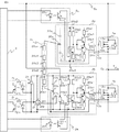
図13は、この発明の実施の形態3による電力変換装置の構成図であり、電力変換主回路1、ゲート駆動回路基板2、制御部3、および周辺部品の構成を図示している。電力変換主回路1は、3レベルの電力変換回路として構成されている。電力変換主回路1の正極には高電位を供給する直流母線5aが接続されている。電力変換主回路1の負極には零電位を供給する直流母線5bが接続されている。さらに、電力変換主回路1の中間電位端子5gには中間電位を供給する直流母線が接続されている。内蔵するスイッチング素子のオン、オフを切り替えることにより、電力変換主回路1は出力端子4より3レベルの電位(高電位、中間電位、零電位)を出力する。
FIG. 13 is a configuration diagram of a power conversion device according to
この実施の形態1における電力変換主回路1は、4つのスイッチング素子1c、1d、1e、1fと、2つの中性点クランプダイオード1g、1hと、から構成される。4つのスイッチング素子1c、1d、1e、1fは、それぞれトランジスタ素子10c、10d、10e、10fとダイオード11c、11d、11e、11fとが逆並列に接続されて構成されている。
The power conversion
電力変換主回路1では、正極側の第1のスイッチング部として、スイッチング素子1cとスイッチング素子1dが直列に接続され、負極側の第2のスイッチング部として、スイッチング素子1eとスイッチング素子1fが直列に接続される。この第1のスイッチング部と第2のスイッチング部は、正極側の下位電位側のスイッチング素子1dと負極側の上位電位側のスイッチング素子1eとで直列に接続される。
In the power conversion
正極側の上位電位側に位置するスイッチング素子1cと下位電位側に位置するスイッチング素子1dとの接続点5dに上位電位側の中性点クランプダイオード1gのカソードが接続される。 The cathode of the neutral point clamp diode 1g on the upper potential side is connected to the connection point 5d between the switching element 1c located on the higher potential side on the positive electrode side and the switching element 1d located on the lower potential side.
中性点クランプダイオード1gのアノードは、下位電位側の中性点クランプダイオード1hのカソードに接続されると共に、直列接続された2つの中性点クランプダイオード1g、1hの接続点は、中間電位端子5gに電気的に接続される。
The anode of the neutral point clamp diode 1g is connected to the cathode of the neutral
一方、負極側の上位電位側に位置するスイッチング素子1eと下位電位側に位置するスイッチング素子1fとの接続点5eに下位電位側の中性点クランプダイオード1hのアノードが接続される。
On the other hand, the anode of the neutral
中性点クランプダイオード1hのカソードは、上述の通り、中間電位端子5gに電気的に接続される。スイッチング素子1dとスイッチング素子1eの接続点5fは、出力端子4として引き出され負荷(図示しない)に接続される。
As described above, the cathode of the neutral
ゲート駆動回路基板2には、4つのゲート駆動回路2l、2m、2n、2oが設けられる。ゲート駆動回路2lとゲート駆動回路2mは、第1のゲート駆動部として、それぞれスイッチング素子1cとスイッチング素子1dに接続される。
The gate
同様に、ゲート駆動回路2nとゲート駆動回路2oは、第2のゲート駆動部として、それぞれスイッチング素子1eとスイッチング素子1fに接続される。ゲート駆動回路2l、2m、2n、2oは、それぞれをスイッチング素子1c、1d、1e、1fを駆動する。
Similarly, the
この発明の実施の形態3による電力変換装置では、図13に示すように、インピーダンス素子2Pの一端2p3は、正極側の下位電位側に位置するスイッチング素子1dを駆動するゲート駆動回路2mの接続端26mに接続されている。インピーダンス素子2Pの他端2p1は、負極側の下位電位側に位置するスイッチング素子1fを駆動するゲート駆動回路2oの接続端26oに接続されている。
In the power conversion device according to
本発明の実施の形態ではコンパレータからなる検出部を2個用いる。コンパレータからなる検出部2qの一端を、インピーダンス素子2pの中間部の接続点2p2に接続する。コンパレータからなる検出部2qの他端は、直流電圧源2qqを介してインピーダンス素子2pの一端2p1に接続する。コンパレータからなる検出部2rの一端を、インピーダンス素子2pの中間部の接続点2p2に接続する。コンパレータからなる検出部2qの他端は、直流電圧源2rrを介してインピーダンス素子2pの一端2p1に接続する。
In the embodiment of the present invention, two detection units composed of comparators are used. One end of the detection unit 2q formed of a comparator is connected to the connection point 2p2 at the intermediate portion of the
電力変換主回路1の出力端子4の電位は高電位、中間電位、零電位のいずれかにあるが、出力端子4の電位によってインピーダンス素子2eの電圧が変化する。検出部2qは、出力端子4の電位が零電位にあるのか中間電位以上(中間電位または高電位)にあるのかを検出し、検出結果を下位側出力電圧信号として送出する。検出部2rは、出力端子4の電位が高電位にあるのか中間電位以下(中間電位または零電位)にあるのかを検出し、検出結果を上位側出力電圧信号として送出する。このように、インピーダンス素子2eの電圧を、検出部2q、2rにより検出することにより、電力変換主回路1の出力端子4の電位が高電位、中間電位、零電位のいずれにあるのかを検出することができる。
Although the potential of the
直流電圧源2qq、2rrの電圧値は直流母線の電位に応じてそれぞれ適切に調整しておく。直流電圧源2qq、2rrはゲート駆動回路2oの電源を用いれば簡単に構成することができる。ゲート駆動回路2oの電源電圧を抵抗分圧すれば所望の電圧値を持つ直流電圧源を得ることができる。あるいは、レギュレータICを用いることにより、ゲート駆動回路2oの電源電圧より所望の電圧値を持つ直流電圧源を得てもよい。 The voltage values of the DC voltage sources 2qq and 2rr are adjusted appropriately according to the potential of the DC bus. The DC voltage sources 2qq and 2rr can be easily configured by using the power source of the gate drive circuit 2o. A DC voltage source having a desired voltage value can be obtained by dividing the power supply voltage of the gate drive circuit 2o by resistance. Alternatively, a DC voltage source having a desired voltage value may be obtained from the power supply voltage of the gate drive circuit 2o by using a regulator IC.
各ゲート駆動回路2l、2m、2n、2oは、それぞれスイッチング素子1c、1d、1e、1fのゲート−ソース間(トランジスタ素子がIGBTの場合はゲート−エミッタ間)に電圧印加できるように電気的に接続し、絶縁回路2x、2y、2ad、2aeを介して入力された各駆動信号に基づき、各スイッチング素子1c、1d、1e、1fにゲート電圧を印加する。
Each of the
検出部2q、2rにより検出された出力電圧信号は、絶縁回路2aa、2acを介して制御部3に出力し、また、反転論理部2t、2uにより反転した反転出力電圧信号も、絶縁回路2z、2abを介して制御部3に出力するように構成する。なお、図13も、図1、図6と同様に、矢印付きの線を信号線、矢印無しの線を電気的配線として図示している。
The output voltage signals detected by the
制御器3は、第1の補正回路であるデッドタイム補正回路3e、第1の付加回路であるデッドタイム付加回路3f、第2の付加回路であるデッドタイム付加回路3g、第2の補正回路であるデッドタイム補正回路3i、第3の付加回路であるデッドタイム付加回路3j、および第4の付加回路であるデッドタイム付加回路3kにより構成される。
The
デッドタイム補正回路3eは、電力変換主回路1の正極側の出力電圧指令値である上位PWM信号を受けて、ゲート駆動回路基板2から入力される上位側出力電圧信号とその反転出力電圧信号に基づきデッドタイム補正を行う。
The dead
デッドタイム付加回路3fは、デッドタイム補正回路3eからのスイッチング素子1cの駆動信号に対してデッドタイムを付加してゲート駆動回路2lに駆動信号を出力する。デッドタイム付加回路3gは、デッドタイム補正回路3eからの信号を反転論理部3hにより反転した第5のスイッチング素子1eの駆動信号に対してデッドタイムを付加してゲート駆動回路2nに駆動信号を出力する。
The dead
デッドタイム補正回路3iは、電力変換主回路1の負極側の出力電圧指令値である下位PWM信号を受けて、ゲート駆動回路基板2から入力された下位側出力電圧信号とその反転出力電圧信号に基づきデッドタイム補正を行う。
The dead
デッドタイム付加回路3jは、デッドタイム補正回路3iからのスイッチング素子1dの駆動信号に対してデッドタイムを付加してゲート駆動回路2mに駆動信号を出力する。デッドタイム付加回路3kは、デッドタイム補正回路3iからの信号を反転論理部3lにより反転したスイッチング素子1fの駆動信号に対してデッドタイムを付加してゲート駆動回路2oに駆動信号を出力する。
The dead
このように、実施の形態3による電力変換装置では、出力端子4から出力される電位状態は3レベル(高電位、中間電位、零電位)のいずれかであるが、出力電位を検出できるように2つの検出部2q、2rを設け、これに対応するように制御部3に、デッドタイム補正回路3e、3iと、デッドタイム付加回路3f、3g、3j、3kを設けた以外は、実施の形態2と同様の構成であるため、ここでは詳細な説明は省略する。
As described above, in the power conversion device according to the third embodiment, the potential state output from the
この構成によれば、3レベルの電圧を出力する場合であっても、基本的に、出力端子4から出力される電圧の検出方法の原理は、実施の形態1と同じであり、実施の形態1および実施の形態2と同様の効果が得られるだけでなく、上位および下位それぞれのPWM信号に対して2レベルの電力変換回路と同様のデッドタイム補正回路を用いることで、3レベルの電力変換回路においてもデッドタイム補正をすることができる。
According to this configuration, even when a three-level voltage is output, the principle of the method for detecting the voltage output from the
実施の形態3では、ゲート駆動回路2l、2m、2n、2o、絶縁回路2x、2y、2ad、2aeといった部品を同一基板であるゲート駆動回路基板2の上に構成している。本発明に特有の部品である、インピーダンス素子2p、検出部2r、2q、絶縁回路2z、2aa、2ab、2acといった部品もゲート駆動回路基板2の上に構成している。このように構成することで、ゲート駆動回路基板の製造時に本発明に特有の部品をゲート駆動回路部品と合わせて実装することができる。本発明の効果を得られる電力変換装置を製造工程が増加することなく製造することができる。
In the third embodiment, components such as
なお、本実施の形態では、直流電圧源2qq、2rrの電圧値は直流母線の電位に応じてそれぞれ適切に調整しておくことを述べた。通常、電力変換装置に電力を供給する直流母線の電位は安定しており、直流電圧源2qq、2rrの電圧値の調整は一度行えば良い。しかしながら、特殊な用途の電力変換装置においては、直流母線の通常時の電位が大きく変動することがある。この場合には検出部2q、2rの閾値をそれぞれ生成する直流電圧源2qq、2rrの電圧値は、直流母線の電位によって可変となるように構成することが望ましい。
In the present embodiment, it has been described that the voltage values of the DC voltage sources 2qq and 2rr are appropriately adjusted according to the potential of the DC bus. Normally, the potential of the DC bus that supplies power to the power converter is stable, and the voltage values of the DC voltage sources 2qq and 2rr need only be adjusted once. However, in a power converter for special applications, the normal potential of the DC bus may fluctuate greatly. In this case, it is desirable that the voltage values of the DC voltage sources 2qq and 2rr that respectively generate the threshold values of the
上記の変形例として、図14に示すように、直流母線5aとゲート駆動回路2oの接続端26oとをインピーダンス素子2afで電気的に接続し、その分圧電位を利用する電力変換装置がある。2個の分圧電位があり、それぞれ直流電圧源2qq、2rrとして用いる。これにより、直流母線5aの通常時の電位が変動しても、それに応じて閾値電圧が変動するため検出部2q、2rの誤検知、誤動作を防止できる。さらに、本構成であれば、落雷などで母線電圧が異常に変動して瞬時低下した場合であっても、検出部2q、2rの誤検知、誤動作を防止できる。
As a modification of the above, as shown in FIG. 14, there is a power converter that electrically connects the
図15では、別の変形例を示す。この電力変換装置は、実施の形態2で説明したゲート駆動回路基板2と同じものを2枚用いて、上位電位側のゲート駆動回路基板2Cはスイッチング素子1cとスイッチング素子1eを駆動するように配線し、下位電位側のゲート駆動回路基板2Dはスイッチング素子1dとスイッチング素子1fを駆動するように配線している。
FIG. 15 shows another modification. This power conversion device uses two identical gate
図15のように構成することで、2レベルの電力変換回路用のゲート駆動回路基板を流用することができることから、設計コストや部品調達コストを低減できる。 With the configuration as shown in FIG. 15, a gate drive circuit board for a two-level power conversion circuit can be used, so that design costs and component procurement costs can be reduced.
以上のように、この発明の実施の形態3における電力変換装置では、実施の形態1および実施の形態2の2レベルの電力変換装置の構成を基本として、3レベルの電力変換主回路に対応するように、出力端子4から出力される各電位差を検出できるように2つの検出部2q、2rを設け、制御部3にデッドタイム補正回路3e、3iおよびデッドタイム付加回路3f、3g、3j、3kを設けることで、3レベルの電圧を出力する場合であっても、実施の形態1および実施の形態2の2レベルの場合と同様の効果を得られる。すなわち、電力変換主回路の出力電圧を検出し、デッドタイム補償する電力変換装置であって、製造が容易で、かつ誤動作しない電力変換装置を得ることができる。また、製造が容易で、かつ誤動作しない電力変換主回路の出力電圧検出方法を得ることができる。
As described above, the power conversion device according to the third embodiment of the present invention basically corresponds to the three-level power conversion main circuit based on the configuration of the two-level power conversion device according to the first and second embodiments. As described above, two
また、3レベルの電力変換主回路に対しても従来技術に比べてフォトカプラのような絶縁素子の遅れ要素に起因する誤差を補正することができ、デッドタイム補正の精度を向上することができる。 In addition, it is possible to correct an error caused by a delay element of an insulating element such as a photocoupler as compared with the prior art for a three-level power conversion main circuit, and to improve the accuracy of dead time correction. .
さらに上述の通り、検出部2r、2qの閾値をそれぞれ生成する直流電圧源2rr、2qqを、直流母線5aの電位によって閾値が可変となるように構成することで、直流母線の電位が変動しても検出部2r、2qの誤検知、誤動作を防止できる。
Furthermore, as described above, the DC voltage sources 2rr and 2qq that generate the threshold values of the
実施の形態4.
実施の形態1では、スイッチング素子1a、1bからなるモジュール100、101とゲート駆動回路2a、2bとが分離して配置されており、配線にて接続されている場合を示した。実施の形態4においては、一体として配置されている場合について示す。
In the first embodiment, the case where the
図16および図17は、この発明の実施の形態4による電力変換装置の配置例を示す図である。ゲート駆動回路2a、ゲート駆動回路2b、インピーダンス素子2e、スイッチング素子1aとスイッチング素子1bからなるモジュール102、および周辺の部品の配置を示す。
16 and 17 are diagrams showing examples of arrangement of the power conversion device according to
モジュール102は、スイッチング素子1aおよびスイッチング素子1bが1つの筐体に納められた、いわゆる2in1モジュールとなっている。ゲート駆動回路2aおよびゲート駆動回路2bは、1枚のゲート駆動回路基板2で構成されている。
The
図16は、ゲート駆動回路2aおよびゲート駆動回路2bを搭載するゲート駆動回路基板2が、スイッチング素子1aとスイッチング素子1bとを収めたモジュール102に載設する前の、分離した状態を示す。
FIG. 16 shows a state where the gate
スイッチング素子1aとスイッチング素子1bとを収めたモジュール102には、制御用ゲート端子12a、12bと制御用ソース端子13a、13bが、金属ピンの形でそれぞれ設けられている。
The
一方、ゲート駆動回路基板2のゲート駆動回路2aとゲート駆動回路2bには、制御用ゲート端子12a、12bと制御用ソース端子13a、13bにそれぞれ対応して、制御用ゲート端子の取り付け部28a、28bと制御用ソース端子の取り付け部29a、29bが、ソケットの形で設けられている。
On the other hand, the
ゲート駆動回路基板2は、矢印Aの方向に従って、モジュール102の直上に載設され、図17に示すように、モジュール102の制御用ゲート端子12a、12bと制御用ソース端子13a、13bが、制御用ゲート端子の取り付け部28a、28bと制御用ソース端子の取り付け部29a、29bを介して、ゲート駆動回路2aおよびゲート駆動回路2bと、それぞれ電気的に接続される。
The gate
このように、外付けのソース信号線およびゲート信号線を用いずにゲート駆動回路基板2をモジュール102の直上に近づけて配置していることから、電磁ノイズの影響を抑え、電力変換主回路の出力端子4の電位が変形することなくインピーダンス素子2eに伝達される。制御部は出力端子4の電位を精度よく検出できる。
As described above, the gate
さらに、インピーダンス素子2eとゲート駆動回路2aの接続端26aがゲート駆動回路2aの制御用ソース端子13aの近傍に配置されている。すなわち、接続端26aと制御用ソース端子13aとの距離は、制御用ゲート端子12aと制御用ソース端子13aとの距離と同じか、それ未満である。また、インピーダンス素子2eとゲート駆動回路2bの接続端26bがゲート駆動回路2bの制御用ソース端子13bの近傍に配置されている。すなわち、接続端26bと制御用ソース端子13bとの距離は、制御用ゲート端子12bと制御用ソース端子13bとの距離と同じか、それ未満である。本構成により、さらに電磁ノイズの影響を抑え、電力変換主回路の出力端子4の電位が変形することなくインピーダンス素子2eに伝達される。制御部は出力端子4の電位をさらに精度よく検出できる。
Further, the
以上のように、この発明の実施の形態4による電力変換装置では、ゲート駆動回路基板2をモジュール102の直上に近づけて配置するだけでなく、インピーダンス素子2eとゲート駆動回路2aの接続端26aが、スイッチング素子1aの制御用ソース端子13aの近傍に配置し、インピーダンス素子2eとゲート駆動回路2bの接続端26bがスイッチング素子1bの制御用ソース端子13bの近傍に配置することで、電磁ノイズの影響を抑え、電力変換主回路の出力端子4の電位が変形することなくインピーダンス素子2eに伝達される。制御部は出力端子4の電位を精度よく検出できる。
As described above, in the power conversion device according to the fourth embodiment of the present invention, not only the gate
なお、この実施の形態4では、実施の形態1の電力変換主回路1とゲート駆動回路基板2との接続の場合について説明したが、これに限るものではない。実施の形態2および実施の形態3での電力変換主回路1とゲート駆動回路基板2の接続に用いた場合にも、同様の効果を得ることができる。
In the fourth embodiment, the connection between the power conversion
また、この実施の形態4では、インピーダンス素子2eを空中配線にゲート駆動回路基板と接続する構成にて説明したが、インピーダンス素子2eが回路パターンにてゲート駆動回路基板2と接続する構成とした場合においても、同様の効果を得ることができる。
In the fourth embodiment, the
以上、実施の形態1から実施の形態4においては、それぞれ電力変換主回路1が1つの構成の場合について説明したが、これに限るものではない。これらの電力変換主回路1をそれぞれ3個並列に構成して三相インバータとして構成してもよい。また、DCDCコンバータとして構成してもよい。さらに、AC/DC変換するPWMコンバータとして構成してもよい。いずれにおいても、この発明の実施の形態1から実施の形態4と同様の効果を得ることができる。
As described above, in the first to fourth embodiments, the case where the power conversion
なお、本実施の形態1から実施の形態4においては、同一の電力変換主回路に属する2個のスイッチング素子に注目し、それぞれのスイッチング素子を駆動するゲート駆動回路の間をインピーダンス素子で接続した。本発明はこの構成に限るものではなく、別々の電力変換主回路に属するスイッチング素子に着目し、それぞれのスイッチング素子を駆動するゲート駆動回路の間をインピーダンス素子で接続してもよい。 In the first to fourth embodiments, attention is paid to two switching elements belonging to the same power conversion main circuit, and the gate drive circuits that drive the respective switching elements are connected by impedance elements. . The present invention is not limited to this configuration, and attention may be paid to switching elements belonging to different power conversion main circuits, and the gate drive circuits that drive the respective switching elements may be connected by impedance elements.
例えば、3相電動機を駆動する3相2レベルインバータを考える。U相正極側のスイッチング素子を駆動するゲート駆動回路とV相正極側のスイッチング素子を駆動するゲート駆動回路をインピーダンス素子2eUVで結ぶ。インピーダンス素子2eUVの電圧または電流を検出器2fUVにより検出すれば、3相2レベルインバータのU相出力とV相出力の相間電圧を検出することができる。同様に、V相正極側のスイッチング素子を駆動するゲート駆動回路とW相正極側のスイッチング素子を駆動するゲート駆動回路をインピーダンス素子2eVWで結ぶ。インピーダンス素子2eVWの電圧または電流を検出器2fVWにより検出すれば、3相2レベルインバータのV相出力とW相出力の相間電圧を検出することができる。W相正極側のスイッチング素子を駆動するゲート駆動回路とU相正極側のスイッチング素子を駆動するゲート駆動回路をインピーダンス素子2eWUで結ぶ。インピーダンス素子2eWUの電圧または電流を検出器2fWUにより検出すれば、3相2レベルインバータのW相出力とU相出力の相間電圧を検出することができる。 For example, consider a three-phase two-level inverter that drives a three-phase motor. A gate driving circuit for driving the switching element on the U-phase positive side and a gate driving circuit for driving the switching element on the V-phase positive side are connected by the impedance element 2eUV. If the voltage or current of the impedance element 2eUV is detected by the detector 2fUV, the phase voltage between the U-phase output and the V-phase output of the three-phase two-level inverter can be detected. Similarly, a gate drive circuit that drives the switching element on the V-phase positive side and a gate drive circuit that drives the switching element on the W-phase positive side are connected by the impedance element 2eVW. If the voltage or current of the impedance element 2eVW is detected by the detector 2fVW, the phase voltage between the V-phase output and the W-phase output of the three-phase two-level inverter can be detected. A gate drive circuit that drives the switching element on the W-phase positive electrode side and a gate drive circuit that drives the switching element on the U-phase positive electrode side are connected by the impedance element 2eWU. If the voltage or current of the impedance element 2eWU is detected by the detector 2fWU, the phase voltage between the W-phase output and the U-phase output of the three-phase two-level inverter can be detected.
3相2レベルインバータの制御部は、検出器2fUV、2fVW、2fWUの出力を受けることにより、3相2レベルインバータが実際に出力した相間電圧を知ることができる。一方で、制御部は、送出したオン指令信号、オフ指令信号から3相2レベルインバータが出力した相間電圧を推定する。制御部は、両者の相間電圧のずれ時間を計ることにより、デッドタイム補正量を得ることができる。デッドタイム補正量を考慮してオン指令信号、オフ指令信号を送出するように制御部を構成すれば、デッドタイム補償を行う電力変換装置を得ることができる。 The controller of the three-phase two-level inverter can know the phase voltage actually output by the three-phase two-level inverter by receiving the outputs of the detectors 2fUV, 2fVW, and 2fWU. On the other hand, the control unit estimates the interphase voltage output by the three-phase two-level inverter from the sent on command signal and off command signal. The control unit can obtain the dead time correction amount by measuring the shift time of the interphase voltage. If the control unit is configured to send the on command signal and the off command signal in consideration of the dead time correction amount, a power conversion device that performs dead time compensation can be obtained.
1 電力変換主回路、1a、1b、1c、1d、1e、1f スイッチング素子、2、2a、2B、2C、2D ゲート駆動回路基板、 2a、2b、2l、2m、2n、2o ゲート駆動回路、2e、2p、2af インピーダンス素子、2f、2q、2r 検出部、2g、2h、2i、2j、2x、2y、2z、2aa、2ab、2ac、2ad、2ae 絶縁回路、3 制御部、3a、3e、3i デッドタイム補正回路、2k、2t、2u 反転論理部、3b、3c、3f、3g、3j、3k デッドタイム付加回路、3d、3h、3l 反転論理部、23a、23b ゲート信号線、24a、24b ソース信号線、100、101、102 モジュール
DESCRIPTION OF
Claims (21)
前記各スイッチング部をそれぞれ駆動する複数のゲート駆動部と、
前記ゲート駆動部の間に接続されるインピーダンス素子と、
前記インピーダンス素子の電圧または電流を検出する検出部と
を備え、
前記インピーダンス素子の一端は前記複数のゲート駆動部のうちの一つと接続され、前記インピーダンス素子の他端は前記一端と接続された前記ゲート駆動部と異なる他の前記複数のゲート駆動部のうちの一つと接続されることを特徴とする電力変換装置。 A power conversion main circuit having two or more switching units;
A plurality of gate driving units for driving each of the switching units;
An impedance element connected between the gate driving units;
A detection unit for detecting the voltage or current of the impedance element ,
One end of the impedance element is connected to one of the plurality of gate driving units, and the other end of the impedance element is different from the gate driving unit connected to the one end. A power conversion device connected to one .
Priority Applications (1)
| Application Number | Priority Date | Filing Date | Title |
|---|---|---|---|
| JP2014176913A JP6261476B2 (en) | 2014-09-01 | 2014-09-01 | Power converter and output voltage detection method of power converter |
Applications Claiming Priority (1)
| Application Number | Priority Date | Filing Date | Title |
|---|---|---|---|
| JP2014176913A JP6261476B2 (en) | 2014-09-01 | 2014-09-01 | Power converter and output voltage detection method of power converter |
Publications (3)
| Publication Number | Publication Date |
|---|---|
| JP2016052198A JP2016052198A (en) | 2016-04-11 |
| JP2016052198A5 JP2016052198A5 (en) | 2016-12-01 |
| JP6261476B2 true JP6261476B2 (en) | 2018-01-17 |
Family
ID=55659359
Family Applications (1)
| Application Number | Title | Priority Date | Filing Date |
|---|---|---|---|
| JP2014176913A Active JP6261476B2 (en) | 2014-09-01 | 2014-09-01 | Power converter and output voltage detection method of power converter |
Country Status (1)
| Country | Link |
|---|---|
| JP (1) | JP6261476B2 (en) |
Families Citing this family (5)
| Publication number | Priority date | Publication date | Assignee | Title |
|---|---|---|---|---|
| FR3068848B1 (en) * | 2017-07-06 | 2019-08-23 | Alstom Transport Technologies | CIRCUIT FOR PROTECTING AGAINST SWITCHING CIRCUITS FOR TRANSISTOR SIC OR GAN MOSFET AND ASSOCIATED METHOD |
| CN111213312B (en) * | 2017-11-17 | 2023-10-20 | 株式会社爱信 | Inverter control substrate |
| JP6973028B2 (en) * | 2017-12-20 | 2021-11-24 | 株式会社デンソー | Buck-boost converter circuit |
| US11831232B2 (en) | 2021-08-13 | 2023-11-28 | General Electric Company | Power converter having a gate drive circuit and method of operating |
| CN117882287A (en) * | 2021-09-06 | 2024-04-12 | 三菱电机株式会社 | Control unit for power converter and power conversion device |
Family Cites Families (3)
| Publication number | Priority date | Publication date | Assignee | Title |
|---|---|---|---|---|
| JPS6277065A (en) * | 1985-09-30 | 1987-04-09 | Mitsubishi Heavy Ind Ltd | Measuring method for output voltage of inverter |
| JPH05252795A (en) * | 1992-03-04 | 1993-09-28 | Toshiba Corp | Digital current controller for inverter |
| JP3429670B2 (en) * | 1998-03-20 | 2003-07-22 | 譲 常広 | Inverter device |
-
2014
- 2014-09-01 JP JP2014176913A patent/JP6261476B2/en active Active
Also Published As
| Publication number | Publication date |
|---|---|
| JP2016052198A (en) | 2016-04-11 |
Similar Documents
| Publication | Publication Date | Title |
|---|---|---|
| JP6261476B2 (en) | Power converter and output voltage detection method of power converter | |
| JP5029900B2 (en) | Motor control device | |
| US10134718B2 (en) | Power semiconductor module | |
| JP6261769B2 (en) | Power conversion device and power semiconductor module | |
| US10050560B1 (en) | Inverter circuit with current detection circuitry | |
| US20140226376A1 (en) | Electronic circuit | |
| KR101992559B1 (en) | Power conversion device | |
| US20180183432A1 (en) | Semiconductor apparatus and inverter system | |
| US11394288B2 (en) | Negative voltage generation circuit and power conversion device using same | |
| US10418893B2 (en) | Fast-switching circuit assembly for a converter | |
| US11711025B2 (en) | Power semiconductor module and power conversion apparatus including the same | |
| US10164530B2 (en) | Boost chopper circuit including switching device circuit and backflow prevention diode circuit | |
| US11050358B2 (en) | Power module with built-in drive circuit | |
| US11016045B2 (en) | Inverter device and method for detecting heat dissipation characteristics of inverter device | |
| JP6483963B2 (en) | Power converter | |
| US10256721B2 (en) | Step-down chopper circuit including a switching device circuit and a backflow prevention diode circuit | |
| JP6476727B2 (en) | Power supply | |
| JP6447436B2 (en) | Power converter | |
| JP2019088078A (en) | Driver circuit and power converter | |
| Mishra et al. | Evaluation of All SiC MOSFET Based Voltage Source Inverter with Open Loop Induction Motor | |
| JP6503977B2 (en) | Control method of power conversion circuit and power conversion module | |
| CN115514188A (en) | Power conversion device |
Legal Events
| Date | Code | Title | Description |
|---|---|---|---|
| A521 | Request for written amendment filed |
Free format text: JAPANESE INTERMEDIATE CODE: A523 Effective date: 20161018 |
|
| A621 | Written request for application examination |
Free format text: JAPANESE INTERMEDIATE CODE: A621 Effective date: 20161018 |
|
| A977 | Report on retrieval |
Free format text: JAPANESE INTERMEDIATE CODE: A971007 Effective date: 20170905 |
|
| A131 | Notification of reasons for refusal |
Free format text: JAPANESE INTERMEDIATE CODE: A131 Effective date: 20170912 |
|
| A521 | Request for written amendment filed |
Free format text: JAPANESE INTERMEDIATE CODE: A523 Effective date: 20171026 |
|
| TRDD | Decision of grant or rejection written | ||
| A01 | Written decision to grant a patent or to grant a registration (utility model) |
Free format text: JAPANESE INTERMEDIATE CODE: A01 Effective date: 20171114 |
|
| A61 | First payment of annual fees (during grant procedure) |
Free format text: JAPANESE INTERMEDIATE CODE: A61 Effective date: 20171212 |
|
| R151 | Written notification of patent or utility model registration |
Ref document number: 6261476 Country of ref document: JP Free format text: JAPANESE INTERMEDIATE CODE: R151 |
|
| R250 | Receipt of annual fees |
Free format text: JAPANESE INTERMEDIATE CODE: R250 |
|
| R250 | Receipt of annual fees |
Free format text: JAPANESE INTERMEDIATE CODE: R250 |
|
| R250 | Receipt of annual fees |
Free format text: JAPANESE INTERMEDIATE CODE: R250 |
|
| R250 | Receipt of annual fees |
Free format text: JAPANESE INTERMEDIATE CODE: R250 |