JP6113220B2 - Solar cell inspection apparatus and solar cell inspection method - Google Patents
Solar cell inspection apparatus and solar cell inspection method Download PDFInfo
- Publication number
- JP6113220B2 JP6113220B2 JP2015095351A JP2015095351A JP6113220B2 JP 6113220 B2 JP6113220 B2 JP 6113220B2 JP 2015095351 A JP2015095351 A JP 2015095351A JP 2015095351 A JP2015095351 A JP 2015095351A JP 6113220 B2 JP6113220 B2 JP 6113220B2
- Authority
- JP
- Japan
- Prior art keywords
- solar cell
- current
- voltage
- cell string
- circuit
- Prior art date
- Legal status (The legal status is an assumption and is not a legal conclusion. Google has not performed a legal analysis and makes no representation as to the accuracy of the status listed.)
- Active
Links
- 238000007689 inspection Methods 0.000 title claims description 103
- 238000000034 method Methods 0.000 title claims description 53
- 239000003990 capacitor Substances 0.000 claims description 42
- 238000001514 detection method Methods 0.000 claims description 39
- 238000010248 power generation Methods 0.000 claims description 25
- 238000007599 discharging Methods 0.000 claims description 3
- 239000000523 sample Substances 0.000 description 7
- 238000003745 diagnosis Methods 0.000 description 6
- 238000010586 diagram Methods 0.000 description 5
- 241000750042 Vini Species 0.000 description 4
- 230000006870 function Effects 0.000 description 4
- 230000007423 decrease Effects 0.000 description 3
- 238000005259 measurement Methods 0.000 description 3
- 230000003247 decreasing effect Effects 0.000 description 2
- 230000005855 radiation Effects 0.000 description 2
- 239000004065 semiconductor Substances 0.000 description 2
- 230000002159 abnormal effect Effects 0.000 description 1
- 238000003491 array Methods 0.000 description 1
- 230000000903 blocking effect Effects 0.000 description 1
- 244000145845 chattering Species 0.000 description 1
- 238000006243 chemical reaction Methods 0.000 description 1
- 230000006866 deterioration Effects 0.000 description 1
- 238000002405 diagnostic procedure Methods 0.000 description 1
- 230000000694 effects Effects 0.000 description 1
- 230000007935 neutral effect Effects 0.000 description 1
Images


Classifications
-
- H—ELECTRICITY
- H02—GENERATION; CONVERSION OR DISTRIBUTION OF ELECTRIC POWER
- H02S—GENERATION OF ELECTRIC POWER BY CONVERSION OF INFRARED RADIATION, VISIBLE LIGHT OR ULTRAVIOLET LIGHT, e.g. USING PHOTOVOLTAIC [PV] MODULES
- H02S50/00—Monitoring or testing of PV systems, e.g. load balancing or fault identification
- H02S50/10—Testing of PV devices, e.g. of PV modules or single PV cells
-
- H—ELECTRICITY
- H02—GENERATION; CONVERSION OR DISTRIBUTION OF ELECTRIC POWER
- H02S—GENERATION OF ELECTRIC POWER BY CONVERSION OF INFRARED RADIATION, VISIBLE LIGHT OR ULTRAVIOLET LIGHT, e.g. USING PHOTOVOLTAIC [PV] MODULES
- H02S50/00—Monitoring or testing of PV systems, e.g. load balancing or fault identification
-
- G—PHYSICS
- G01—MEASURING; TESTING
- G01N—INVESTIGATING OR ANALYSING MATERIALS BY DETERMINING THEIR CHEMICAL OR PHYSICAL PROPERTIES
- G01N21/00—Investigating or analysing materials by the use of optical means, i.e. using sub-millimetre waves, infrared, visible or ultraviolet light
- G01N21/84—Systems specially adapted for particular applications
- G01N21/88—Investigating the presence of flaws or contamination
-
- G—PHYSICS
- G01—MEASURING; TESTING
- G01R—MEASURING ELECTRIC VARIABLES; MEASURING MAGNETIC VARIABLES
- G01R31/00—Arrangements for testing electric properties; Arrangements for locating electric faults; Arrangements for electrical testing characterised by what is being tested not provided for elsewhere
- G01R31/26—Testing of individual semiconductor devices
-
- G—PHYSICS
- G01—MEASURING; TESTING
- G01R—MEASURING ELECTRIC VARIABLES; MEASURING MAGNETIC VARIABLES
- G01R31/00—Arrangements for testing electric properties; Arrangements for locating electric faults; Arrangements for electrical testing characterised by what is being tested not provided for elsewhere
- G01R31/28—Testing of electronic circuits, e.g. by signal tracer
-
- Y—GENERAL TAGGING OF NEW TECHNOLOGICAL DEVELOPMENTS; GENERAL TAGGING OF CROSS-SECTIONAL TECHNOLOGIES SPANNING OVER SEVERAL SECTIONS OF THE IPC; TECHNICAL SUBJECTS COVERED BY FORMER USPC CROSS-REFERENCE ART COLLECTIONS [XRACs] AND DIGESTS
- Y02—TECHNOLOGIES OR APPLICATIONS FOR MITIGATION OR ADAPTATION AGAINST CLIMATE CHANGE
- Y02E—REDUCTION OF GREENHOUSE GAS [GHG] EMISSIONS, RELATED TO ENERGY GENERATION, TRANSMISSION OR DISTRIBUTION
- Y02E10/00—Energy generation through renewable energy sources
- Y02E10/50—Photovoltaic [PV] energy
Description
本発明は、太陽電池に使用されているバイパスダイオードの検査を実行する太陽電池検査装置および太陽電池検査方法に関するものである。 The present invention relates to a solar cell inspection device and a solar cell inspection method for inspecting a bypass diode used in a solar cell.
この種の太陽電池検査装置の一例として、下記の特許文献1に開示された太陽電池検査装置(パワーコンディショナ)が知られている。この太陽電池検査装置は、太陽電池アレイと接続されており、太陽電池アレイを流れる電流の電流値を検出して検出値を出力する電流センサ、太陽電池アレイの両端子間の電圧を検出して検出値を出力する電圧センサ、入力コンデンサ、電流センサ及び電圧センサの検出値に基づいて、太陽電池アレイの出力電力が最大になる点を追従するMPPT(Maximum Power Point Tracking)制御を行うMPPT制御部、太陽電池アレイから出力された直流電流を交流電流に変換して負荷へ出力するためのDC−ACインバータ、商用電源からの交流電流を直流電流に変換するAC−DCコンバータ、発電時と診断時とで配線の切り替えを行うための2つのスイッチ、太陽電池アレイおよび太陽電池アレイのバイパスダイオードの診断処理の制御を行うCPU、及び各種情報を記憶したメモリを含んで構成されている。
As an example of this type of solar cell inspection device, a solar cell inspection device (power conditioner) disclosed in
この場合、入力コンデンサは、発電時の入力コンデンサとして機能するだけでなく、診断時には、太陽電池アレイのI−V特性およびバイパスダイオードのI−V特性を取得するために、その放電特性が利用される。また、電流センサ及び電圧センサは、MPPT制御に用いられる電流及び電圧を検出する機能だけでなく、診断時には、太陽電池アレイのI−V特性を取得するための電流及び電圧を検出するためのセンサとしても用いられる。 In this case, the input capacitor functions not only as an input capacitor during power generation, but also at the time of diagnosis, the discharge characteristic is used to acquire the IV characteristic of the solar cell array and the IV characteristic of the bypass diode. The In addition, the current sensor and the voltage sensor are not only a function for detecting the current and voltage used for MPPT control, but also a sensor for detecting the current and voltage for acquiring the IV characteristics of the solar cell array at the time of diagnosis. Also used as
この特許文献1に開示された太陽電池検査装置では、太陽光発電システムが発電していない時間帯に予め定められた診断時期において、発電用配線側に接続されていた一方のスイッチを中立にして太陽電池アレイと太陽電池検査装置(パワーコンディショナ)との接続を切り、DC−ACインバータ側に接続されていた他方のスイッチをAC−DCコンバータ側に切り替える。そして、商用電源からの交流電流をAC−DCコンバータで変換した直流電流で入力コンデンサを充電する。この充電に際して、特にバイパスダイオードのI−V特性を取得する場合には、放電時にバイパスダイオードの順方向へ放電されるように充電する。充電完了後は、他方のスイッチを中立にして入力コンデンサとAC−DCコンバータとを切り離す。
In the solar cell inspection apparatus disclosed in
次に、検査対象とするバイパスダイオードを含む太陽電池ストリングスを発電用配線側から診断用配線側に切り替える。次いで、一方のスイッチを診断用配線側へ接続し、充電された入力コンデンサを放電させる。そして、この放電時の電流値及び電圧値を電流センサ及び電圧センサから取得して、取得した電流値及び電圧値から検査対象とする太陽電池ストリングスについてのI−V特性を計測する。この場合、入力コンデンサを放電させた際の電流はバイパスダイオードの順方向に流れる電流であるため、太陽電池ストリングスに含まれているバイパスダイオードがすべて正常であるときのI−V特性と、太陽電池ストリングスに含まれているバイパスダイオードのいずれかがオープン状態で故障しているときのI−V特性とは相違する。 Next, the solar cell string including the bypass diode to be inspected is switched from the power generation wiring side to the diagnosis wiring side. Next, one switch is connected to the diagnostic wiring side, and the charged input capacitor is discharged. And the current value and voltage value at the time of this discharge are acquired from a current sensor and a voltage sensor, and the IV characteristic about the solar cell string to be examined is measured from the acquired current value and voltage value. In this case, since the current when the input capacitor is discharged is the current that flows in the forward direction of the bypass diode, the IV characteristics when all the bypass diodes included in the solar cell string are normal, and the solar cell This is different from the IV characteristic when any of the bypass diodes included in the string is broken in an open state.
したがって、この特許文献1に開示された太陽電池検査装置によれば、メモリに記憶させる各種情報の1つとして、バイパスダイオードがすべて正常であるときのI−V特性を記憶させておき、メモリに記憶させたこの正常時のI−V特性と計測されたI−V特性とを比較することにより、バイパスダイオードのいずれかがオープン状態で故障しているか否かを診断することが可能となっている。
Therefore, according to the solar cell inspection device disclosed in
ところが、上記した太陽電池検査装置には、以下のような解決すべき課題が存在している。すなわち、この太陽電池検査装置には、太陽電池が発電していないとき(または、発電量が極めて少ないとき)にしか診断が行えないという課題が存在している。 However, the solar cell inspection apparatus described above has the following problems to be solved. That is, this solar cell inspection apparatus has a problem that diagnosis can be performed only when the solar cell is not generating power (or when the amount of power generation is extremely small).
本発明は、かかる課題を解決するためになされたものであり、太陽電池が発電状態にあるときにおいても太陽電池を検査し得る太陽電池検査装置を提供することを主目的とする。 This invention is made | formed in order to solve this subject, and it aims at providing the solar cell test | inspection apparatus which can test | inspect a solar cell even when a solar cell is in an electric power generation state.
上記目的を達成すべく請求項1記載の太陽電池検査装置は、太陽電池およびバイパスダイオードを有する複数の太陽電池モジュールが直列接続されて構成された太陽電池ストリングにおける前記バイパスダイオードについてのオープン故障の有無を検査する太陽電池検査装置であって、前記太陽電池が発電状態のときに前記太陽電池ストリングから出力される出力電流の通過を許容する極性で当該太陽電池ストリングの正極および負極間に接続される一方向性素子と、前記一方向性素子が接続された前記太陽電池ストリングの前記正極および前記負極間に、当該正極の電位を基準として当該負極の電位が高電位となる電圧であって、複数の前記バイパスダイオードの順方向電圧の総和を上回る電圧値の試験電圧を印加可能な電圧印加部と、前記太陽電池ストリングに流れる電流を検出する電流検出部と、前記発電状態で、かつ前記太陽電池ストリングの前記正極および前記負極間に前記一方向性素子が接続されている短絡状態において前記電流検出部で検出された前記電流に基づいて当該太陽電池ストリングについての短絡電流の電流値を測定すると共に当該短絡電流の電流値よりも高い電流値を電流閾値として記憶する処理、および当該発電状態で、かつ当該短絡状態において前記試験電圧の印加時に前記電流検出部によって検出される前記電流に基づいて測定される最大電流値と前記電流閾値とを比較することにより、前記オープン故障の有無を検査する処理を実行する処理部とを備えている。
In order to achieve the above object, the solar cell inspection apparatus according to
請求項2記載の太陽電池検査装置は、請求項1記載の太陽電池検査装置において、前記電圧印加部は、コンデンサおよび電流制限抵抗の直列回路、電源、並びに前記直列回路が前記電源に接続される充電接続状態と前記直列回路が前記太陽電池ストリングの前記正極および前記負極間に接続される放電接続状態とを切り替える切替部を備え、前記充電接続状態に切り替えるときに、前記切替部を制御して前記電源を前記直列回路に接続させて当該電源から出力される直流電圧で前記コンデンサを充電させ、前記放電接続状態に切り替えるときに、前記切替部を制御して前記直列回路を前記太陽電池ストリングの前記正極および前記負極間に接続させて、前記充電接続状態において充電された前記コンデンサの充電電圧を当該正極および当該負極間に前記試験電圧として印加させる。
The solar cell inspection device according to
請求項3記載の太陽電池検査装置は、請求項2記載の太陽電池検査装置において、前記処理部は、前記充電電圧が予め規定された上限電圧値に達するまで当該充電電圧を徐々に上昇させつつ前記試験電圧として印加させる制御を前記電圧印加部に対して実行する。
The solar cell inspection device according to claim 3 is the solar cell inspection device according to
請求項4記載の太陽電池検査装置は、請求項1から4のいずれかに記載の太陽電池検査装置において、前記試験電圧の印加時に前記バイパスダイオードに流れる電流の上限値を制限する電流制限回路を備えている。
請求項5記載の太陽電池検査方法は、太陽電池およびバイパスダイオードを有する複数の太陽電池モジュールが直列接続されて構成された太陽電池ストリングにおける前記バイパスダイオードについてのオープン故障の有無を検査する太陽電池検査方法であって、前記太陽電池が発電状態のときに前記太陽電池ストリングから出力される出力電流の通過を許容する極性で当該太陽電池ストリングの正極および負極間に一方向性素子を接続した短絡状態において、前記太陽電池ストリングに流れる短絡電流を検出すると共に当該短絡電流の電流値よりも高い電流値を電流閾値として記憶させる処理と、当該発電状態で、かつ当該短絡状態において前記太陽電池ストリングの前記正極および前記負極間に、当該正極の電位を基準として当該負極の電位が高電位となる電圧であって、複数の前記バイパスダイオードの順方向電圧の総和を上回る電圧値の試験電圧の印加時に検出される前記電流に基づいて測定される最大電流値と前記電流閾値とを比較することにより、前記オープン故障の有無を検査する処理を実行する。
The solar cell inspection device according to
The solar cell inspection method according to claim 5, wherein a solar cell inspection for inspecting whether or not there is an open failure in the bypass diode in a solar cell string configured by connecting a plurality of solar cell modules having a solar cell and a bypass diode in series. A short circuit state in which a unidirectional element is connected between a positive electrode and a negative electrode of the solar cell string with a polarity that allows passage of an output current output from the solar cell string when the solar cell is in a power generation state. in the previous SL and process for storing the current value higher than the current value of the short-circuit current as a current threshold and detects the short-circuit current flowing in the solar cell string, in the power generation state, and of the solar cell string in the short-circuit state Between the positive electrode and the negative electrode, the potential of the negative electrode is based on the potential of the positive electrode. Position is a voltage as a high potential, the maximum current value and the current threshold value which is determined on the basis of the current applied is detected during the test voltage of the voltage value exceeding the sum of the forward voltages of the plurality of bypass diodes by comparing the bets, it executes a process of inspecting the presence or absence of the open failure.
請求項1記載の太陽電池検査装置および請求項5記載の太陽電池検査方法では、一方向性素子によって短絡されている短絡状態において発電状態の太陽電池ストリングに流れる短絡電流を検出すると共にこの短絡電流の電流値よりも高い電流値を電流閾値として記憶し、発電状態で、かつこの短絡状態において太陽電池ストリングの正極および負極間に、正極の電位を基準として負極の電位が高電位となる電圧であって、バイパスダイオードの順方向電圧の総和を上回る電圧値の試験電圧を印加したときに電流検出部で検出される電流に基づいて測定される最大電流値と電流閾値とを比較して、バイパスダイオードについてのオープン故障の有無を検査する。
In the solar cell inspection device according to
したがって、この太陽電池検査装置およびこの太陽電池検査方法によれば、太陽電池ストリングが発電状態にあり、その開放電圧が極めて高い電圧であっても、一方向性素子で短絡されることで、太陽電池ストリング内の複数のバイパスダイオードをオン状態に移行させるための試験電圧がこれらのバイパスダイオードの順方向電圧の総和よりも若干高い程度の低い電圧(上記の開放電圧と比べて極めて低い電圧)で済ますことができる。このため、太陽電池ストリングが発電状態であっても、バイパスダイオードについてのオープン故障の有無を確実かつ容易に検査することができる。 Therefore, according to this solar cell inspection device and this solar cell inspection method, even if the solar cell string is in a power generation state and the open circuit voltage is extremely high, the solar cell string is short-circuited by the unidirectional element, The test voltage for shifting the plurality of bypass diodes in the battery string to the ON state is a low voltage that is slightly higher than the sum of the forward voltages of these bypass diodes (very low voltage compared to the above open voltage). I can do it. For this reason, even if the solar cell string is in a power generation state, it is possible to reliably and easily inspect for the presence or absence of an open failure in the bypass diode.
請求項2記載の太陽電池検査装置によれば、バイポーラ電源のような高価な電源を使用することなく、電圧印加部を、コンデンサおよび電流制限抵抗の直列回路と、電源(ユニポーラ電源)と、切替部(例えばスイッチ)とで、簡易に構成することができ、これにより、太陽電池検査装置を安価に製造することができる。
According to the solar cell inspection apparatus of
請求項3記載の太陽電池検査装置によれば、電圧印加部から太陽電池ストリングに印加される試験電圧を徐々に上昇させることができるため、例えば、電流検出部で検出されたこの試験電圧の印加の前後の電流を比較してバイパスダイオードが正常であることを検出した時点で、試験電圧の印加を中止することで、過度の試験電圧の印加に起因してバイパスダイオードが故障するという事態の発生を未然に防止することができる。
請求項4記載の太陽電池検査装置によれば、電流制限回路で制限するバイパスダイオードに流れる電流の上限値を、例えば、バイパスダイオードの尖頭順電流未満に規定することで、バイパスダイオードの数が様々な各種の太陽電池ストリングを検査対象とする場合であっても、過電流に起因したバイパスダイオードの故障を回避しつつ、検査対象とする太陽電池ストリングのうちのバイパスダイオードの数が最も多い太陽電池ストリング内のバイパスダイオードをオン状態に移行させ得る上限電圧を最初から試験電圧として印加することができる。したがって、一回の試験電圧の印加でバイパスダイオードのオープン故障の有無を検査することができるため、検査に要する時間を短縮することができる。
According to the solar cell inspection apparatus of claim 3, since the test voltage applied to the solar cell string from the voltage application unit can be gradually increased, for example, application of this test voltage detected by the current detection unit When the current before and after the current is detected and the bypass diode is detected to be normal, the application of the test voltage is stopped, resulting in the failure of the bypass diode due to the excessive application of the test voltage. Can be prevented in advance.
According to the solar cell inspection device of
以下、太陽電池検査装置および太陽電池検査方法の実施の形態について、添付図面を参照して説明する。 Hereinafter, embodiments of a solar cell inspection device and a solar cell inspection method will be described with reference to the accompanying drawings.
最初に、太陽電池検査装置の構成について、図面を参照して説明する。 First, the configuration of the solar cell inspection apparatus will be described with reference to the drawings.
まず、図1に示す太陽電池検査装置としての太陽電池検査装置1の構成について説明する。
First, the structure of the solar
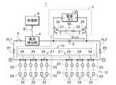
太陽電池検査装置1は、一方向性素子(例えば、ダイオードや、ダイオード接続されたトランジスタなど。本例では一例としてダイオード)2、電圧印加部3、電流検出部4、スイッチ5および処理部6を備えて、後述の太陽電池ストリング12を検査対象としてその中に配設されているバイパスダイオード24についてのオープン故障の有無を検査する。
The solar
ここで、太陽電池検査装置1の各構成要素についての具体的な説明の前に、太陽電池ストリング12の概要について説明する。太陽電池ストリング12は、例えば、ビルや住宅などの建物に設置されている図2に示すような太陽電池アレイ11の構成単位であり、複数個で1つの太陽電池アレイ11を構成している。また、複数の太陽電池ストリング12は、例えば、接続箱13内において、ブロッキングダイオード14を介して並列接続されている。また、各太陽電池ストリング12は、接続箱13内に配設されたスイッチ15により、他の太陽電池ストリング12から切り離したり、並列接続状態に戻したりすることが可能になっている。
Here, an outline of the
また、太陽電池ストリング12は、図1,2に示すように、複数の太陽電池モジュール21が直列接続されて構成され、さらに各太陽電池モジュール21は、複数のクラスタ22が直列接続されて構成されている。また、各クラスタ22は、直列接続された複数の太陽電池セル(太陽電池)23と、この直列接続された複数の太陽電池セル23における全体としての出力端子間(クラスタ22の出力端子間)に接続されたバイパスダイオード24とを備えて構成されている。バイパスダイオード24は、複数の太陽電池セル23における全体としての正側の出力端子にカソード端子が接続され、負側の出力端子にアノード端子が接続されている。
1 and 2, the
この構成により、バイパスダイオード24は、1つのクラスタ22を構成する直列接続された複数の太陽電池セル23内において、負側の出力端子から正側の出力端子に向かう電流(直流電流)が流れ難くなる状況(例えば、木陰に入るなどの状況)が生じたときに、他のクラスタ22から流れ込む電流をバイパスさせることで、太陽電池ストリング12からの電流(直流電流)の出力を継続させる。
With this configuration, in the
次いで、太陽電池検査装置1の各構成要素について個別に説明する。ダイオード2は、図1に示すように、太陽電池セル23が発電状態のときに太陽電池ストリング12から出力される出力電流Ioの通過を許容する極性(出力電流Ioに対して順方向となる極性)で太陽電池ストリング12の正極P1および負極P2間に接続される。本例では一例として、ダイオード2は電流検出部4およびスイッチ5と直列に接続され、これらの部材で構成される直列回路が、プローブPL1,PL2などを介して、太陽電池ストリング12の正極P1および負極P2間に接続される。出力電流Ioを検出する電流検出部4は、一般的な電流計と基本構成は同じであることから、理想的には内部抵抗が極めてゼロオームに近い状態となっている。したがって、スイッチ5がオン状態に移行したときには、ダイオード2は、太陽電池ストリング12を短絡させる。
Next, each component of the solar
電圧印加部3は、ダイオード2の両端子間に、ダイオード2のアノード端子の電位を基準としてカソード端子が高電位となる試験電圧Vtstを印加可能に構成されている。この構成により、電圧印加部3は、太陽電池ストリング12に太陽電池検査装置1が接続されて、太陽電池検査装置1のダイオード2(具体的には、ダイオード2、電流検出部4およびスイッチ5の直列回路)によって太陽電池ストリング12が短絡されているときには、太陽電池ストリング12の正極P1および負極P2間に、正極P1の電位を基準として負極P2が高電位となる試験電圧Vtstを印加可能となっている。
The voltage application unit 3 is configured to be able to apply a test voltage Vtst between the two terminals of the
また、本例では、電圧印加部3は、少なくとも初期電圧値Viniから上限電圧値Vmaxまでの範囲内の電圧値で試験電圧Vtstを出力可能に構成されている。この場合、初期電圧値Viniは、検査対象として想定される種々の太陽電池ストリング12内に配設されているバイパスダイオード24の順方向電圧をVfとし、この種々の太陽電池ストリング12のうちのバイパスダイオード24の数の最も少ない太陽電池ストリング12でのバイパスダイオード24の個数をn1個としたときに、直列に接続されたこの個数n1のバイパスダイオード24の順方向電圧Vfの総和(電圧値:n1×Vf)に、後述する電流制限抵抗32での電圧降下分を加えた電圧値を若干上回る電圧値(つまり、この個数n1のバイパスダイオード24を同時にオン状態にさせ得る電圧値)である。また、上限電圧値Vmaxは、バイパスダイオード24の数の最も多い太陽電池ストリング12でのバイパスダイオード24の個数をn2個としたときのこの個数n2のバイパスダイオード24の順方向電圧Vfの総和(電圧値:n2×Vf)を使用して算出される電圧値である。
Further, in this example, the voltage application unit 3 is configured to be able to output the test voltage Vtst at a voltage value within a range from at least the initial voltage value Vini to the upper limit voltage value Vmax. In this case, the initial voltage value Vini is set to Vf as the forward voltage of the
具体的には、電圧印加部3は、図1に示すように、一例として、コンデンサ31および電流制限抵抗(コンデンサ31の放電時に流れる電流を大まかな電流値に制限する抵抗)32の直列回路SCと、電源(直流電源)33と、切替部としての一対のスイッチ34,35(一極双投型のスイッチ)とを備えている。この場合、一例として、スイッチ34,35の各c接点間に直列回路SCが接続され、スイッチ34のa接点に電源33の負極が接続され、スイッチ35のa接点に電源33の正極が接続されている。また、スイッチ34のb接点(電圧印加部3の出力端子として機能する部位)にダイオード2のアノード端子が接続され、スイッチ35のb接点(電圧印加部3の出力端子として機能する部位)にダイオード2のカソード端子が接続されている。なお、スイッチ34,35は、例えばリレーなどの有接点スイッチで構成することもできるし、オフ・オンする際におけるチャタリングの発生を回避するためにトランジスタやサイリスタなどの半導体スイッチ(無接点スイッチ)で構成することもできる。
Specifically, as illustrated in FIG. 1, the voltage application unit 3 includes, as an example, a series circuit SC of a
電源33は、例えば可変電圧電源(ユニポーラ電源)で構成されて、処理部6によって制御されることにより、処理部6によって設定された電圧値で直流電圧V1を出力する。また、各スイッチ34,35は、処理部6によって制御されることにより、c接点とa接点とが接続される接続状態(充電接続状態)、およびc接点とb接点とが接続される接続状態(放電接続状態)のうちの一方の接続状態に選択的に切り替えられる。
The
この構成により、電圧印加部3では、各スイッチ34,35が処理部6によって制御されて充電接続状態に切り替えられたときには、直列回路SCを構成するコンデンサ31が、電源33から出力される直流電圧V1によってこの直流電圧V1の電圧値(この電圧値についても符号V1で表し、以下、電圧値V1という)と同じ電圧値V1に充電される。また、電圧印加部3は、この状態で各スイッチ34,35が処理部6によって制御されて放電接続状態に切り替えられたときには、コンデンサ31に充電されている直流電圧V1を、ダイオード2間(つまり、スイッチ5がオン状態のときには、ダイオード2によって短絡される太陽電池ストリング12間)に、上記の極性で試験電圧Vtstとして印加する。なお、電源33については、上記のようにコンデンサ31を充電させるだけの電力を供給できればよいため、例えば、乾電池と昇圧回路とを組み合わせて、簡易に構成することもできる。
With this configuration, in the voltage application unit 3, when the
電流検出部4は、上記のように、ダイオード2およびスイッチ5と直列に接続された状態で、太陽電池ストリング12の正極P1および負極P2間にプローブPL1,PL2を介して接続される。この電流検出部4は、例えば電流電圧変換回路を備えて構成されて、通過する電流を検出して電圧に変換し、この変換した電圧を電圧信号Si(通過する電流の電流値に比例して電圧値が変化する信号)として処理部6に出力する。
As described above, the
スイッチ5は、例えば、トランジスタやサイリスタなどの半導体スイッチ(無接点スイッチ)で構成されて、オフ・オンする際におけるアークの発生が回避されている。また、スイッチ5は、処理部6によって制御されることにより、オン状態およびオフ状態のうちの一方の状態に選択的に切り替えられる。また、スイッチ5は、上記のように、ダイオード2および電流検出部4と直列に接続された状態で、太陽電池ストリング12の正極P1および負極P2間にプローブPL1,PL2を介して接続される。
The switch 5 is constituted by, for example, a semiconductor switch (non-contact switch) such as a transistor or a thyristor, and an arc is avoided when the switch 5 is turned on / off. Further, the switch 5 is selectively switched to one of an on state and an off state by being controlled by the processing unit 6. In addition, the switch 5 is connected between the positive electrode P1 and the negative electrode P2 of the
処理部6は、例えば、A/D変換器、メモリおよびCPUなどを備えて、電圧印加部3に対する制御処理(具体的には、電源33に対して直流電圧V1の電圧値V1を設定する処理および直流電圧V1の出力の開始・停止を制御する処理、並びに各スイッチ34,35を切り替える処理)と、電流検出部4から出力される電圧信号Siに基づいて電流検出部4に流れる電流の電流波形を測定する波形測定処理と、スイッチ5に対する制御処理(スイッチ5を切り替える処理)と、検査対象として太陽電池検査装置1にプローブPL1,PL2を介して接続されている太陽電池ストリング12のバイパスダイオード24について検査する(バイパスダイオード24についてのオープン故障の有無を検査する)バイパスダイオード検査処理50(図3参照)とを実行可能に構成されている。なお、処理部6のメモリには、上記の初期電圧値Vini、上記の上限電圧値Vmax、および直流電圧V1の電圧値V1を徐々に上昇させる(本例では一例として、段階的に上昇させる)際の変更幅(単位電圧ΔV)が予め記憶されている。
The processing unit 6 includes, for example, an A / D converter, a memory, a CPU, and the like, and performs control processing for the voltage application unit 3 (specifically, processing for setting the voltage value V1 of the DC voltage V1 for the power supply 33). And the process of controlling the start / stop of the output of the DC voltage V1 and the process of switching the
また、処理部6は、バイパスダイオード検査処理50の結果を出力する出力処理についても実行可能に構成されている。この出力処理では、太陽電池検査装置1にディスプレイ装置などの出力装置を設けて、この出力装置に検査の結果を出力したり、太陽電池検査装置1の外部に設けられた他の装置に対して検査の結果を出力したりすることができる。
Further, the processing unit 6 is configured to be able to execute an output process for outputting a result of the bypass
次に、太陽電池検査装置1を用いて太陽電池ストリング12のバイパスダイオード24を検査する際の太陽電池検査装置1の動作を、太陽電池検査方法と併せて図3を参照して説明する。なお、太陽電池ストリング12の各太陽電池セル23は正常であるものとする。
Next, operation | movement of the solar cell test |
建物に設置されている太陽電池アレイ11を構成している複数の太陽電池ストリング12のバイパスダイオード24について検査する際には、この太陽電池アレイ11が接続されている接続箱13内の各スイッチ15のうちの検査対象として太陽電池検査装置1に接続する1つの太陽電池ストリング12に対応するスイッチ15をオン状態からオフ状態に切り替えて、他の太陽電池ストリング12から切り離し、この切り離された状態の1つの太陽電池ストリング12の正極P1および負極P2間にプローブPL1,PL2を介して太陽電池検査装置1を接続するという操作を、全ての太陽電池ストリング12のバイパスダイオード24についての検査が完了するまで繰り返す。
When inspecting the
太陽電池検査装置1では、検査対象とする1つの太陽電池ストリング12(検査対象とするバイパスダイオード24を含む太陽電池ストリング12)がプローブPL1,PL2を介して接続されている状態において、図3に示すバイパスダイオード検査処理50を実行する。
In the solar
このバイパスダイオード検査処理50では、処理部6は、まず、太陽電池ストリング12を短絡させる処理を実行する(ステップ51)。この処理では、処理部6は、スイッチ5に対する制御処理を実行して、初期状態においてオフ状態となっているスイッチ5をオン状態に切り替える。これにより、オン状態のスイッチ5および内部抵抗が極めてゼロオームに近い状態の電流検出部4と共に、太陽電池ストリング12からの出力電流Ioの通過を許容する極性のダイオード2が、プローブPL1,PL2を介して太陽電池ストリング12の正極P1および負極P2間に直列に接続される。このため、太陽電池ストリング12は、ダイオード2、電流検出部4およびスイッチ5の直列回路によって短絡される。
In the bypass
次いで、処理部6は、この短絡状態において太陽電池ストリング12から出力される出力電流Io(短絡状態での出力電流Ioであることから、特に短絡電流Isともいう)を測定する処理を実行する(ステップ52)。具体的には、処理部6は、この処理において、まず、波形測定処理を実行して、電流検出部4から出力される電圧信号Siに基づいて電流検出部4に流れている短絡電流Isの電流波形(図4参照)を測定して記憶する。次いで、処理部6は、この記憶した電流波形に基づいて短絡電流Isの電流値を測定し、この測定した電流値よりも若干高い電流値(例えば、数%程度高い電流値)を、バイパスダイオード24の検査の際に使用する電流閾値Ith(図4参照)として記憶する。この場合、1回のバイパスダイオード検査処理50に要する時間(実質的にコンデンサ31の放電波形が観測できればよいため、短絡電流Isの測定に要する時間を含め、数ms〜数10ms)のように日照状態の変化に要する時間と比較して十分に短い時間においては、太陽電池アレイ11に対する日照量はほぼ一定とみなすことができる。このため、短絡電流Isは、図4において実線で示すように、その電流値がほぼ一定で推移する直流電流の電流波形となる。
Next, the processing unit 6 performs a process of measuring the output current Io output from the
なお、バイパスダイオード検査処理50を実行する都度、電流閾値Ithを測定して記憶する構成を採用することにより、太陽電池アレイ11に対する日射量(つまり、太陽電池ストリング12に対する日射量)の増減に応じて電流閾値Ithを増減させることができるため、この電流閾値Ithを後述するように使用するバイパスダイオード24の検査の精度を向上させることが可能になっている。
By adopting a configuration in which the current threshold Ith is measured and stored each time the bypass
続いて、処理部6は、電圧印加部3に対する制御処理を実行して、電源33から出力される直流電圧V1の電圧値V1を初期電圧値Viniに設定する(ステップ53)。
Subsequently, the processing unit 6 executes a control process for the voltage application unit 3, and sets the voltage value V1 of the DC voltage V1 output from the
次いで、処理部6は、電圧印加部3に対する制御処理を実行して、コンデンサ31を直流電圧V1に充電する(ステップ54)。具体的には、このステップ54では、処理部6は、まず、各スイッチ34,35を切り替える処理を実行して、コンデンサ31および電流制限抵抗32の直列回路SCを電源33に接続し、次いで、電源33に対して直流電圧V1の出力を開始させる。これにより、コンデンサ31は、直流電圧V1(スイッチ34側の端子の電位を基準として、スイッチ35側の端子が電圧値V1だけ高電位となる状態)に充電される。
Next, the processing unit 6 executes a control process for the voltage application unit 3 to charge the
続いて、処理部6は、電圧印加部3に対する制御処理を実行して、コンデンサ31をダイオード2側に接続して放電させると共に、このコンデンサ31の放電時に電流検出部4に流れる電流の最大電流値(ピーク値)Ipを測定する(ステップ55)。具体的には、このステップ55では、処理部6は、各スイッチ34,35を切り替える処理を実行して、コンデンサ31および電流制限抵抗32の直列回路SCをダイオード2に接続する。これにより、コンデンサ31に充電されている直流電圧V1が、アノード端子の電位を基準としてカソード端子の電位が高電位となる状態でダイオード2に印加され、ひいてはこのダイオード2によって短絡されている太陽電池ストリング12に試験電圧Vtstとして印加される。また、処理部6は、この試験電圧Vtstの印加後に、電圧印加部3に対する制御処理を実行して、電源33に対して直流電圧V1の出力を停止させる。
Subsequently, the processing unit 6 executes a control process for the voltage application unit 3 to connect the
また、処理部6は、この試験電圧Vtstの印加の開始から予め規定された時間だけ、波形測定処理を実行して、電流検出部4から出力される電圧信号Siに基づいて電流検出部4に流れている電流の電流波形を測定し、この電流波形に基づいて、電流検出部4に流れている電流の最大電流値(ピーク値)Ipを測定して記憶する。
Further, the processing unit 6 executes the waveform measurement process for a predetermined time from the start of application of the test voltage Vtst, and sends the
次いで、処理部6は、測定したピーク値Ipと、ステップ52において記憶した電流閾値Ithとを比較する(ステップ56)。 Next, the processing unit 6 compares the measured peak value Ip with the current threshold Ith stored in Step 52 (Step 56).
この場合、試験電圧Vtstは、図1に示すように、太陽電池ストリング12内の複数のバイパスダイオード24全体に対して、カソード端子に対してアノード端子が高電位となる極性で印加される(順方向で印加される)。このため、試験電圧Vtstが検査中の太陽電池ストリング12内の複数のバイパスダイオード24の順方向電圧値Vfの総和を上回る電圧値であって(第1条件)、かつこれらのバイパスダイオード24がすべて正常であるとき(第2条件)には、試験電圧Vtstの印加により、これらのすべてのバイパスダイオード24がオン状態に移行する。
In this case, as shown in FIG. 1, the test voltage Vtst is applied to the entire plurality of
したがって、この際には、コンデンサ31に充電されている電荷が、電圧印加部3から太陽電池ストリング12の負極P2、太陽電池ストリング12の直列接続されたオン状態の各バイパスダイオード24、太陽電池ストリング12の正極P1、オン状態のスイッチ5および電流検出部42を介して電圧印加部3に至る電流経路に流れ、これに伴い、試験電圧Vtstの印加の直後の期間において、図4に示すように、電流検出部4に流れる電流の電流波形に短絡電流Isの電流波形を超えるピークが現れる。また、上記したように、電流閾値Ithがこの短絡電流Isの電流値よりも若干だけ高い電流値に規定されていることから、このピークについてのピーク値Ipは、殆どの場合、この電流閾値Ithを上回る状態となる。
Accordingly, at this time, the electric charge charged in the
このため、処理部6は、このステップ56での比較の結果、ピーク値Ipが電流閾値Ithを上回る状態となったことを検出したときには、検査中の太陽電池ストリング12内のすべてのバイパスダイオード24が正常であると判別し、出力処理を実行して、バイパスダイオード24が正常である旨の検査結果を出力する(ステップ57)。なお、充電されている電荷の放電の結果、コンデンサ31の電圧がバイパスダイオード24の順方向電圧値Vfの総和以下となったときには、すべてのバイパスダイオード24がオン状態からオフ状態に戻ることから、電流検出部4には流れる電流は、図4に示すように、太陽電池ストリング12からの短絡電流Isだけとなる。この場合、コンデンサ31に残存している電荷はこの短絡電流Isの一部として流れ(コンデンサ31の放電は継続され)、コンデンサ31の電圧は、次第に減少してほぼゼロボルト(具体的には、ダイオード2の順方向電圧)に至る。
Therefore, when the processing unit 6 detects that the peak value Ip has exceeded the current threshold value Ith as a result of the comparison in
処理部6は、このステップ57の実行後は、スイッチ5に対する制御処理を実行して、スイッチ5をオフ状態(初期状態)に切り替える。これにより、ダイオード2、電流検出部4およびスイッチ5の直列回路による太陽電池ストリング12の短絡が解除されて(ステップ58)、バイパスダイオード検査処理50が完了する。
After executing
一方、ステップ56での比較の結果、ピーク値Ipが電流閾値Ith以下となっていることを検出したとき(実際には、短絡電流Is以下のピークは観測できないため、ピークが現れない短絡電流Isのみが観測されたとき)には、処理部6は、上記した第1条件が満たされていない、つまり試験電圧Vtstが太陽電池ストリング12内の複数のバイパスダイオード24の順方向電圧値Vfの総和に達していないと判別して、現在の電圧値V1にメモリに記憶されている単位電圧ΔVを加算して得られる電圧値を直流電圧V1ついての新たな電圧値V1の候補として算出する(ステップ59)。なお、この場合には、図5に示すように、破線で示すコンデンサ31の放電に起因して発生する電流は、短絡電流Isの一部として流れるため、コンデンサ31の放電状態においても、電流検出部4で検出される電流は、太陽電池ストリング12からの短絡電流Isだけとなっている。また、コンデンサ31は放電されて、その電圧は次第に減少してほぼゼロボルト(具体的には、ダイオード2の順方向電圧)に至る。
On the other hand, as a result of the comparison in
また、処理部6は、このようにして、より高い新たな電圧値V1を算出したときには、この新たな電圧値V1と、メモリに記憶されている上限電圧値Vmaxとを比較して、電圧値V1が上限電圧値Vmaxを上回っていないか否かを判別する(ステップ60)。この結果、電圧値V1が上限電圧値Vmaxを上回っていないとき(V1>Vmaxではないとき)には、処理部6は、上記したステップ54に移行して、電圧印加部3に対する制御処理を実行することで、コンデンサ31を新たな電圧値V1の直流電圧V1で充電する。
In addition, when the processing unit 6 calculates a new new voltage value V1 in this manner, the processing unit 6 compares the new voltage value V1 with the upper limit voltage value Vmax stored in the memory, and thereby compares the voltage value. It is determined whether or not V1 exceeds the upper limit voltage value Vmax (step 60). As a result, when the voltage value V1 does not exceed the upper limit voltage value Vmax (when V1> Vmax is not satisfied), the processing unit 6 proceeds to the above-described
その後、処理部6は、ステップ54、ステップ55、ステップ56、ステップ59およびステップ60を繰り返し実行しつつ、ステップ59において算出する新たな電圧値V1が、ステップ60での比較において上限電圧値Vmaxを上回るまでの間に、ステップ56での比較の結果が「ピーク値Ipが電流閾値Ithを上回る」との比較結果となったときには、検査中の太陽電池ストリング12内のすべてのバイパスダイオード24が正常であると判別すると共にその検査結果を出力し(ステップ57)、太陽電池ストリング12の短絡を解除して(ステップ58)、バイパスダイオード検査処理50を完了させる。
Thereafter, the processing unit 6 repeatedly executes
また、処理部6は、ステップ54、ステップ55、ステップ56、ステップ59およびステップ60を繰り返し実行している状態において、ステップ56での比較の結果が「ピーク値Ipが電流閾値Ithを上回る」との比較結果となる前に、ステップ59で算出する新たな電圧値V1が、ステップ60での比較において上限電圧値Vmaxを上回ったことを検出したときには、検査中の太陽電池ストリング12内の少なくとも1つのバイパスダイオード24がオープン故障であると判別し、出力処理を実行して、その旨の検査結果を出力する(ステップ61)。
Further, in the state where the processing unit 6 repeatedly executes
この際にオープン故障であると判別する理由としては、上記した第1条件が満たされている(つまり、検査対象として想定されている太陽電池ストリング12のうちのバイパスダイオード24の個数が最大(n2個)の太陽電池ストリング12であっても、上限電圧値Vmaxは、これらのバイパスダイオード24の順方向電圧Vfの総和(n2×Vf)を上回っている)にも拘わらず、バイパスダイオード24がオン状態に移行しないのは、上記した第2条件(バイパスダイオード24がすべて正常であるとの条件)が満たされていない、つまり、検査中の太陽電池ストリング12内の少なくとも1つのバイパスダイオード24がオープン故障だからである。この場合、コンデンサ31の電荷は短絡電流Isの一部として流れ、コンデンサ31の電圧は、次第に低下してほぼゼロボルト(具体的には、ダイオード2の順方向電圧)に至る。
At this time, the reason for determining an open failure is that the first condition described above is satisfied (that is, the number of
処理部6は、このステップ61の実行後は、スイッチ5に対する制御を実行して、スイッチ5をオフ状態(初期状態)に切り替える。これにより、ダイオード2、電流検出部4およびスイッチ5の直列回路による太陽電池ストリング12の短絡が解除されて(ステップ58)、バイパスダイオード検査処理50が完了する。
After executing
このように、この太陽電池検査装置1および太陽電池検査方法では、太陽電池ストリング12におけるバイパスダイオード24についてのオープン故障の有無を検査する際に、太陽電池セル23が発電状態のときに太陽電池ストリング12から出力される出力電流Ioの通過を許容する極性で太陽電池ストリング12の正極P1および負極P2間にダイオード2を接続した状態において、ダイオード2が接続された太陽電池ストリング12(接続されたダイオード2によって短絡されている太陽電池ストリング12)の正極P1および負極P2間に、正極P1の電位を基準として負極P2の電位が高電位となる電圧であって、複数のバイパスダイオード24の順方向電圧Vfの総和を上回る電圧値V1の試験電圧Vtstを印加し、電流検出部4で検出されたこの試験電圧Vtstの印加の前後の電流を比較して(上記の例では、試験電圧Vtstの印加の前の短絡電流Isに基づいて決定された電流閾値Ithと、試験電圧Vtstの印加の後の電流のピーク値Ipとを比較して)、バイパスダイオード24についてのオープン故障の有無を検査する。
Thus, in this solar
したがって、この太陽電池検査装置1および太陽電池検査方法によれば、太陽電池ストリング12(つまり太陽電池セル23)が発電状態にあり、その開放電圧が極めて高い電圧(一例として、最大級の太陽電池ストリング12(直列に接続された太陽電池モジュール21の数は30個であり、1つの太陽電池モジュール21において3つのクラスタ22が直列接続されている太陽電池ストリング12)では約1000V)であっても、ダイオード2で短絡されることで、太陽電池ストリング12内の複数のバイパスダイオード24をオン状態に移行させるための試験電圧Vtstがこれらのバイパスダイオード24の順方向電圧Vfの総和よりも若干高い程度の低い電圧(上記の例では、1つの太陽電池ストリング12内のバイパスダイオード24の個数は90個(=30×3)であり、この総和は、順方向電圧Vfを例えば0.6Vとしたときに54Vとなって、1000Vと比較して極めて低い電圧となる)で済ますことができる。このため、太陽電池ストリングが発電状態であっても、バイパスダイオードについてのオープン故障の有無を確実かつ容易に検査することができる。
Therefore, according to the solar
また、この太陽電池検査装置1および太陽電池検査方法によれば、バイポーラ電源のような高価な電源を使用することなく、上記した例のように、電圧印加部3を、コンデンサ31および電流制限抵抗32の直列回路SCと、電源33と、切替部としての一対のスイッチ34,35(一極双投型のスイッチ)とで、簡易に構成することができる。このため、太陽電池検査装置1を安価に製造することができる。
Further, according to the solar
また、この太陽電池検査装置1および太陽電池検査方法では、処理部6は、コンデンサ31の充電電圧(電圧値V1)が予め規定された上限電圧値Vmaxに達するまで、この充電電圧を徐々に上昇させつつ試験電圧Vtstとして印加させる制御を電圧印加部3に対して実行する。上記したように、検査対象としての太陽電池ストリング12内に配設されているバイパスダイオード24の個数は、建物に設置されている太陽電池アレイ11によって相違する場合がある。この場合、検査対象としての太陽電池ストリング12のうちのバイパスダイオード24が最も多い太陽電池ストリング12内のバイパスダイオード24をオン状態に移行させ得る上限電圧値Vmaxを最初から試験電圧Vtstとして印加させる構成を採用することも考えられるが、この構成では、例えば、バイパスダイオード24が少ない太陽電池ストリング12に対して、過度の試験電圧Vtstが印加される状態となることがあり、これに起因してバイパスダイオード24に過電流が流れることで、バイパスダイオード24が故障を引き起こすおそれがある。
In the solar
一方、この太陽電池検査装置1および太陽電池検査方法によれば、電圧印加部3から太陽電池ストリング12に印加される試験電圧Vtstを徐々に上昇させることができるため、電流検出部4で検出されたこの試験電圧Vtstの印加の前後の電流を比較してバイパスダイオード24が正常であることを検出した時点で、試験電圧Vtstの印加を中止することで、過度の試験電圧Vtstの印加に起因してバイパスダイオード24が故障するという事態の発生を未然に防止することができる。
On the other hand, according to the solar
なお、内部に配設されているバイパスダイオード24の個数が既知の太陽電池ストリング12を検査対象とするときには、太陽電池ストリング12に印加される試験電圧Vtstを徐々に上昇させる上記の構成に代えて、これらのバイパスダイオード24の順方向電圧Vfの総和から算出される試験電圧Vtstを最初から印加する構成を採用してもよいのは勿論である。
When the
また、図6に示すように、試験電圧Vtstの印加に起因してバイパスダイオード24に流れる電流の上限値を制限値に制限する電流制限回路7をこの電流経路に配置する構成を採用することもできる。なお、同図では、電圧印加部3の外部に電流制限回路7を配置する構成であるが、電圧印加部3の内部に配置する構成であってもよい。電流制限回路7を配置する場合、電流制限回路7のこの制限値をバイパスダイオード24の尖頭順電流未満に規定することで、バイパスダイオード24の数が様々な各種の太陽電池ストリング12を検査対象とする場合であっても、過電流に起因したバイパスダイオード24の故障を回避しつつ、検査対象とする太陽電池ストリング12のうちのバイパスダイオード24の数が最も多い太陽電池ストリング12内のバイパスダイオード24をオン状態に移行させ得る上限電圧Vmaxを最初から試験電圧Vtstとして印加させる構成を採用することができる。一般に太陽電池モジュールで使用されているバイパスダイオードの詳細はモジュールメーカから公開されていない場合が多く、尖頭順電流を知ることは困難であるが、発電電流を異常クラスタをバイパスさせて流すといったバイパスダイオードの目的から考えて、太陽電池モジュールの仕様として記載されている短絡電流は必ず流せるはずである。このため、電流制限回路7の制限値は、ステップ52で観測される短絡電流Isの2倍(短絡電流Is+バイパスダイオードに流す電流)に制限することが望ましい(これは、電流制限回路7は処理部6によって制御されることを意味する)。この場合、図1に示す電圧印加部3の直列回路SCを構成している電流制限抵抗32は放電時には不要となる。一方、電源33によるコンデンサ31の充電の際には、充電電流を制限する必要がある。したがって、電流制限抵抗32は、図1に示す位置に代えて、図6に示すように電源33とスイッチ34との間、および図示はしないが電源33とスイッチ35との間の少なくとも一方に配置する構成を採用する。この構成によれば、一回の試験電圧Vtstの印加でバイパスダイオード24のオープン故障の有無を検査することができ、検査に要する時間を短縮することができる。
Further, as shown in FIG. 6, it is also possible to employ a configuration in which a current limiting
また、上記したように、建物に設置されている1つの太陽電池アレイ11を構成している複数の太陽電池ストリング12のバイパスダイオード24について検査する際には、検査対象とする1つの太陽電池ストリング12を、他の太陽電池ストリング12から切り離して太陽電池検査装置1に接続するという操作を、全ての太陽電池ストリング12について実行する。このため、この太陽電池検査装置1および太陽電池検査方法では、各太陽電池ストリング12についての試験電圧Vtstの印加時の電流波形を取得することができる。したがって、例えば、正常時に太陽電池ストリング12のバイパスダイオード24に流れる電流のピーク値Ipを、他の太陽電池ストリング12のものと比較することにより、バイパスダイオード24のインピーダンスの変化(劣化の度合い)を検出することもできる。
Further, as described above, when inspecting the
また、上記の例では、電流検出部4で検出された試験電圧Vtstの印加の前後の電流を比較する構成の一例として、試験電圧Vtstの印加の前の短絡電流Isに基づいて決定された電流閾値Ithと、試験電圧Vtstの印加の後の電流のピーク値Ipとを比較する構成を採用しているが、すべてのバイパスダイオード24が正常であるときには、図4に示すように電流検出部4で検出される電流の波形にスパイク状(尖塔状)の波形が現れるのに対して、いずれかのバイパスダイオード24がオープン故障しているときには、図5に示すように、このスパイク状(尖塔状)の波形が現れないことに着目して、電流検出部4で検出された試験電圧Vtstの印加の前後の電流の波形を比較する構成を採用することもできる。
In the above example, as an example of the configuration for comparing the current before and after the application of the test voltage Vtst detected by the
また、電流検出部4の配設位置は、図1に示す位置に限定されない。電流検出部4は、試験電圧Vtstの印加によってバイパスダイオード24がオン状態に移行したときに流れるスパイク状の電流の電流経路(太陽電池ストリング12の正極P1から、スイッチ5および電圧印加部3を経由して負極P2に至る電流経路)内の任意の位置に配設することができる。したがって、ダイオード2の両端間に接続される電圧印加部3側にも、電流検出部3を配置することもできる。具体的には、電流検出部4を、スイッチ34のb接点とダイオード2のアノード端子との間、およびスイッチ35のb接点とダイオード2のカソード端子との間のいずれか一方の位置に配設することもできる。さらには、電流検出部4を電圧印加部3内に、直列回路SCと直列に配設することもできる(電流検出部4を電圧印加部3と一体化させることもできる)。
Further, the arrangement position of the
また、上記したように、太陽電池ストリング12は一般的には複数の太陽電池モジュール21が直列接続されて構成されているが、太陽電池ストリング12が1つの太陽電池モジュール21で構成されている太陽電池アレイ11では、検査対象である太陽電池ストリング12が太陽電池モジュール21自体となる。
As described above, the
1 太陽電池検査装置
2 ダイオード(一方向性素子)
3 電圧印加部
4 電流検出部
6 処理部
12 太陽電池ストリング
21 太陽電池モジュール
22 クラスタ
23 太陽電池(太陽電池セル)
24 バイパスダイオード
31 コンデンサ
32 電流制限抵抗
33 電源
34,35 スイッチ
Io 出力電流
SC 直列回路
V1 直流電圧
Vtst 試験電圧
DESCRIPTION OF
DESCRIPTION OF SYMBOLS 3
24
Claims (5)
前記太陽電池が発電状態のときに前記太陽電池ストリングから出力される出力電流の通過を許容する極性で当該太陽電池ストリングの正極および負極間に接続される一方向性素子と、
前記一方向性素子が接続された前記太陽電池ストリングの前記正極および前記負極間に、当該正極の電位を基準として当該負極の電位が高電位となる電圧であって、複数の前記バイパスダイオードの順方向電圧の総和を上回る電圧値の試験電圧を印加可能な電圧印加部と、
前記太陽電池ストリングに流れる電流を検出する電流検出部と、
前記発電状態で、かつ前記太陽電池ストリングの前記正極および前記負極間に前記一方向性素子が接続されている短絡状態において前記電流検出部で検出された前記電流に基づいて当該太陽電池ストリングについての短絡電流の電流値を測定すると共に当該短絡電流の電流値よりも高い電流値を電流閾値として記憶する処理、および当該発電状態で、かつ当該短絡状態において前記試験電圧の印加時に前記電流検出部によって検出される前記電流に基づいて測定される最大電流値と前記電流閾値とを比較することにより、前記オープン故障の有無を検査する処理を実行する処理部とを備えている太陽電池検査装置。 A solar cell inspection device that inspects whether or not there is an open failure for the bypass diode in a solar cell string configured by connecting a plurality of solar cell modules having a solar cell and a bypass diode in series,
A unidirectional element connected between a positive electrode and a negative electrode of the solar cell string with a polarity that allows passage of an output current output from the solar cell string when the solar cell is in a power generation state;
Between the positive electrode and the negative electrode of the solar cell string to which the unidirectional element is connected, a voltage at which the potential of the negative electrode becomes a high potential with reference to the potential of the positive electrode, and the order of the plurality of bypass diodes A voltage application unit capable of applying a test voltage having a voltage value exceeding the sum of the directional voltages;
A current detector for detecting a current flowing in the solar cell string;
About the solar cell string based on the current detected by the current detection unit in the power generation state and in a short-circuit state in which the unidirectional element is connected between the positive electrode and the negative electrode of the solar cell string A process of measuring the current value of the short-circuit current and storing a current value higher than the current value of the short-circuit current as a current threshold, and in the power generation state, and by applying the test voltage in the short-circuit state by the current detection unit A solar cell inspection apparatus comprising: a processing unit that performs a process of inspecting the presence or absence of the open failure by comparing a maximum current value measured based on the detected current and the current threshold .
前記太陽電池が発電状態のときに前記太陽電池ストリングから出力される出力電流の通過を許容する極性で当該太陽電池ストリングの正極および負極間に一方向性素子を接続した短絡状態において、前記太陽電池ストリングに流れる短絡電流を検出すると共に当該短絡電流の電流値よりも高い電流値を電流閾値として記憶させる処理と、当該発電状態で、かつ当該短絡状態において前記太陽電池ストリングの前記正極および前記負極間に、当該正極の電位を基準として当該負極の電位が高電位となる電圧であって、複数の前記バイパスダイオードの順方向電圧の総和を上回る電圧値の試験電圧の印加時に検出される前記電流に基づいて測定される最大電流値と前記電流閾値とを比較することにより、前記オープン故障の有無を検査する処理を実行する太陽電池検査方法。 A solar cell inspection method for inspecting the presence or absence of an open failure for the bypass diode in a solar cell string configured by connecting a plurality of solar cell modules having a solar cell and a bypass diode in series,
In short-circuit state of connecting the unidirectional element passes in polarity to allow between the positive electrode and the negative electrode of the solar cell string of the output current output from the solar cell string when the solar cell power generation state, before Symbol sun A process of detecting a short-circuit current flowing in the battery string and storing a current value higher than the current value of the short-circuit current as a current threshold; and the positive electrode and the negative electrode of the solar cell string in the power generation state and in the short-circuit state In between, the current detected at the time of applying a test voltage having a voltage value that is higher than the total of forward voltages of the plurality of bypass diodes, the voltage at which the potential of the negative electrode becomes a high potential with reference to the potential of the positive electrode by the comparing the current threshold and the maximum current value measured on the basis of, the process of inspecting the presence or absence of the open fault Solar cell inspection how to row.
Priority Applications (5)
| Application Number | Priority Date | Filing Date | Title |
|---|---|---|---|
| JP2015095351A JP6113220B2 (en) | 2015-05-08 | 2015-05-08 | Solar cell inspection apparatus and solar cell inspection method |
| CN201610269523.5A CN106130475B (en) | 2015-05-08 | 2016-04-27 | Inspecting apparatus for photovoltaic devices and solar cell inspection method |
| US15/139,605 US9762179B2 (en) | 2015-05-08 | 2016-04-27 | Solar cell testing apparatus and solar cell testing method |
| EP16167898.2A EP3091658B1 (en) | 2015-05-08 | 2016-05-02 | Solar cell testing apparatus and solar cell testing method |
| US15/670,053 US9831828B1 (en) | 2015-05-08 | 2017-08-07 | Solar cell testing apparatus and solar cell testing method |
Applications Claiming Priority (1)
| Application Number | Priority Date | Filing Date | Title |
|---|---|---|---|
| JP2015095351A JP6113220B2 (en) | 2015-05-08 | 2015-05-08 | Solar cell inspection apparatus and solar cell inspection method |
Publications (3)
| Publication Number | Publication Date |
|---|---|
| JP2016213955A JP2016213955A (en) | 2016-12-15 |
| JP2016213955A5 JP2016213955A5 (en) | 2017-04-06 |
| JP6113220B2 true JP6113220B2 (en) | 2017-04-12 |
Family
ID=55919632
Family Applications (1)
| Application Number | Title | Priority Date | Filing Date |
|---|---|---|---|
| JP2015095351A Active JP6113220B2 (en) | 2015-05-08 | 2015-05-08 | Solar cell inspection apparatus and solar cell inspection method |
Country Status (4)
| Country | Link |
|---|---|
| US (2) | US9762179B2 (en) |
| EP (1) | EP3091658B1 (en) |
| JP (1) | JP6113220B2 (en) |
| CN (1) | CN106130475B (en) |
Families Citing this family (16)
| Publication number | Priority date | Publication date | Assignee | Title |
|---|---|---|---|---|
| DE102013101314A1 (en) | 2013-02-11 | 2014-08-14 | Phoenix Contact Gmbh & Co. Kg | Safe photovoltaic system |
| DE102015209612A1 (en) * | 2015-05-26 | 2016-12-01 | Saint-Augustin Canada Electric Inc. | Method for testing the chip attachment of a photovoltaic cell array |
| DE102015114755A1 (en) * | 2015-09-03 | 2017-03-09 | Phoenix Contact Gmbh & Co. Kg | Safe photovoltaic system |
| JP6829099B2 (en) * | 2016-02-17 | 2021-02-10 | 日置電機株式会社 | Solar cell inspection device and solar cell inspection method |
| EP3288086A1 (en) * | 2016-08-26 | 2018-02-28 | LG Electronics Inc. | Solar cell module and method for manufacturing the same |
| US10177576B2 (en) * | 2016-09-20 | 2019-01-08 | Richtek Technology Corporation | Charger circuit and capacitive power conversion circuit and reverse blocking switch circuit thereof |
| JP6536552B2 (en) * | 2016-12-12 | 2019-07-03 | トヨタ自動車株式会社 | Solar power system |
| JP6821477B2 (en) * | 2017-03-14 | 2021-01-27 | 日置電機株式会社 | Solar cell inspection device and solar cell inspection method |
| JP6821478B2 (en) * | 2017-03-15 | 2021-01-27 | 日置電機株式会社 | Solar cell inspection device |
| CN107452826B (en) * | 2017-07-26 | 2019-10-29 | 河北曹妃甸汉能薄膜太阳能有限公司 | Hull cell terminal plate, sub- battery component and its assemble method |
| CN109600115B (en) * | 2017-09-30 | 2020-12-29 | 丰郅(上海)新能源科技有限公司 | Method for locating faults in series-connected photovoltaic power generation system |
| CN108233868A (en) * | 2017-12-23 | 2018-06-29 | 四川大学 | A kind of photovoltaic device Current Voltage test platform of variable temperature and angle adjustable |
| CN108333495B (en) * | 2018-03-01 | 2020-11-03 | 国家电投集团西安太阳能电力有限公司 | Method for detecting working state of bypass diode of photovoltaic module junction box |
| JP7448956B2 (en) | 2018-12-13 | 2024-03-13 | 学校法人帝京大学 | Method for estimating the operating voltage of a solar cell in a solar cell module and system for estimating the operating voltage of a solar cell |
| CN110146801B (en) * | 2019-05-13 | 2021-10-01 | 西北核技术研究院 | Nondestructive testing method for parameters of solar cell bypass diode |
| TWI723851B (en) * | 2020-04-21 | 2021-04-01 | 友達光電股份有限公司 | Inspection system of a solar cell |
Family Cites Families (12)
| Publication number | Priority date | Publication date | Assignee | Title |
|---|---|---|---|---|
| JP2000059986A (en) * | 1998-04-08 | 2000-02-25 | Canon Inc | Solar cell module and method and device of failure detection therefor |
| DE102008008504A1 (en) | 2008-02-11 | 2009-08-13 | Siemens Aktiengesellschaft | Method for theft detection of a PV module and failure detection of a bypass diode of a PV module as well as corresponding PV sub-generator junction box, PV inverter and corresponding PV system |
| JP5403608B2 (en) | 2009-09-18 | 2014-01-29 | 学校法人東京理科大学 | Solar cell array diagnostic method and power conditioner |
| US9324885B2 (en) * | 2009-10-02 | 2016-04-26 | Tigo Energy, Inc. | Systems and methods to provide enhanced diode bypass paths |
| US9423448B1 (en) * | 2011-03-06 | 2016-08-23 | Sunpower Corporation | Testing of module integrated electronics using power reversal |
| JP5691816B2 (en) * | 2011-05-11 | 2015-04-01 | 日立金属株式会社 | Abnormality detection device for solar panel |
| JP5465221B2 (en) * | 2011-09-30 | 2014-04-09 | 三菱電機株式会社 | Photovoltaic power generation system and photovoltaic power generation management system |
| JP5759911B2 (en) * | 2012-01-30 | 2015-08-05 | Jx日鉱日石エネルギー株式会社 | Solar cell unit and solar cell module |
| CN102638197B (en) * | 2012-04-20 | 2014-11-12 | 浙江昱能科技有限公司 | Solar photovoltaic component, method for tracking maximum power point thereof and method for monitoring fault thereof |
| JP5841906B2 (en) * | 2012-07-03 | 2016-01-13 | Jx日鉱日石エネルギー株式会社 | Failure detection device, failure detection system, and failure detection method |
| WO2015037663A1 (en) * | 2013-09-11 | 2015-03-19 | 独立行政法人宇宙航空研究開発機構 | Solar cell adjustment system, related method, and minimum current detection and control system |
| JP2016123232A (en) * | 2014-12-25 | 2016-07-07 | 日置電機株式会社 | Solar cell inspection method and device for the same, and signal source used for solar cell inspection device |
-
2015
- 2015-05-08 JP JP2015095351A patent/JP6113220B2/en active Active
-
2016
- 2016-04-27 US US15/139,605 patent/US9762179B2/en active Active
- 2016-04-27 CN CN201610269523.5A patent/CN106130475B/en active Active
- 2016-05-02 EP EP16167898.2A patent/EP3091658B1/en active Active
-
2017
- 2017-08-07 US US15/670,053 patent/US9831828B1/en active Active
Also Published As
| Publication number | Publication date |
|---|---|
| JP2016213955A (en) | 2016-12-15 |
| EP3091658A1 (en) | 2016-11-09 |
| EP3091658B1 (en) | 2018-08-29 |
| CN106130475B (en) | 2018-04-24 |
| US20160329863A1 (en) | 2016-11-10 |
| CN106130475A (en) | 2016-11-16 |
| US9831828B1 (en) | 2017-11-28 |
| US9762179B2 (en) | 2017-09-12 |
| US20170338770A1 (en) | 2017-11-23 |
Similar Documents
| Publication | Publication Date | Title |
|---|---|---|
| JP6113220B2 (en) | Solar cell inspection apparatus and solar cell inspection method | |
| JP5841906B2 (en) | Failure detection device, failure detection system, and failure detection method | |
| US10411479B2 (en) | Detection circuit and detection method for detecting insulation resistance of photovoltaic inverter, and photovoltaic inverter | |
| JP2016213955A5 (en) | ||
| JP5888724B2 (en) | SOLAR CELL ARRAY DIAGNOSIS DEVICE, POWER CONDITIONER, SOLAR CELL ARRAY DIAGNOSIS METHOD, AND PROGRAM | |
| EP2741093A1 (en) | Ground fault detection device, ground fault detection method, solar energy system, and ground fault detection program | |
| JP2014011428A (en) | Failure detection device, failure detection system, and failure detection method | |
| JP2011066320A (en) | Diagnosis method for solar cell array, and power conditioner | |
| US9024640B2 (en) | Active diagnostics and ground fault detection on photovoltaic strings | |
| JP6470490B2 (en) | Power generation failure detection method, power generation failure detection device and solar power generation device for solar cell string | |
| JP6390359B2 (en) | Inspection method and inspection apparatus for photovoltaic power generation system | |
| JP2013055132A (en) | Method of fault diagnosis of photovoltaic power generation system | |
| WO2015015836A1 (en) | Solar power generation system | |
| JP2014038961A (en) | Conduction failure detection device and conduction failure detection method | |
| WO2014007255A1 (en) | Current control apparatus for solar cell inspection | |
| JP6710583B2 (en) | Solar cell inspection device and solar cell inspection method | |
| JP6702168B2 (en) | Solar power generation system inspection device and inspection method | |
| US9697961B2 (en) | Photovoltaic bypass switching | |
| JP2014011429A (en) | Conduction failure detection device, conduction failure detection system, and conduction failure detection method | |
| Sakthivel et al. | Detection, Classification, and Location of Open-Circuit and Short-Circuit Faults in Solar Photovoltaic Array: An Approach Using Single Sensor | |
| JP6240634B2 (en) | Bypass diode failure inspection system | |
| JP6829099B2 (en) | Solar cell inspection device and solar cell inspection method | |
| JP6821477B2 (en) | Solar cell inspection device and solar cell inspection method | |
| US9121876B2 (en) | Generated power output measuring apparatus |
Legal Events
| Date | Code | Title | Description |
|---|---|---|---|
| A521 | Request for written amendment filed |
Free format text: JAPANESE INTERMEDIATE CODE: A523 Effective date: 20170228 |
|
| A621 | Written request for application examination |
Free format text: JAPANESE INTERMEDIATE CODE: A621 Effective date: 20170228 |
|
| A871 | Explanation of circumstances concerning accelerated examination |
Free format text: JAPANESE INTERMEDIATE CODE: A871 Effective date: 20170228 |
|
| A975 | Report on accelerated examination |
Free format text: JAPANESE INTERMEDIATE CODE: A971005 Effective date: 20170306 |
|
| TRDD | Decision of grant or rejection written | ||
| A01 | Written decision to grant a patent or to grant a registration (utility model) |
Free format text: JAPANESE INTERMEDIATE CODE: A01 Effective date: 20170314 |
|
| A61 | First payment of annual fees (during grant procedure) |
Free format text: JAPANESE INTERMEDIATE CODE: A61 Effective date: 20170314 |
|
| R150 | Certificate of patent or registration of utility model |
Ref document number: 6113220 Country of ref document: JP Free format text: JAPANESE INTERMEDIATE CODE: R150 |
|
| R250 | Receipt of annual fees |
Free format text: JAPANESE INTERMEDIATE CODE: R250 |
|
| R250 | Receipt of annual fees |
Free format text: JAPANESE INTERMEDIATE CODE: R250 |
|
| R250 | Receipt of annual fees |
Free format text: JAPANESE INTERMEDIATE CODE: R250 |