JP6021438B2 - Inverter device - Google Patents
Inverter device Download PDFInfo
- Publication number
- JP6021438B2 JP6021438B2 JP2012119741A JP2012119741A JP6021438B2 JP 6021438 B2 JP6021438 B2 JP 6021438B2 JP 2012119741 A JP2012119741 A JP 2012119741A JP 2012119741 A JP2012119741 A JP 2012119741A JP 6021438 B2 JP6021438 B2 JP 6021438B2
- Authority
- JP
- Japan
- Prior art keywords
- switching elements
- bridge
- current
- main bridge
- positive
- Prior art date
- Legal status (The legal status is an assumption and is not a legal conclusion. Google has not performed a legal analysis and makes no representation as to the accuracy of the status listed.)
- Expired - Fee Related
Links
Images


Classifications
-
- H—ELECTRICITY
- H02—GENERATION; CONVERSION OR DISTRIBUTION OF ELECTRIC POWER
- H02M—APPARATUS FOR CONVERSION BETWEEN AC AND AC, BETWEEN AC AND DC, OR BETWEEN DC AND DC, AND FOR USE WITH MAINS OR SIMILAR POWER SUPPLY SYSTEMS; CONVERSION OF DC OR AC INPUT POWER INTO SURGE OUTPUT POWER; CONTROL OR REGULATION THEREOF
- H02M7/00—Conversion of ac power input into dc power output; Conversion of dc power input into ac power output
- H02M7/42—Conversion of dc power input into ac power output without possibility of reversal
- H02M7/44—Conversion of dc power input into ac power output without possibility of reversal by static converters
- H02M7/48—Conversion of dc power input into ac power output without possibility of reversal by static converters using discharge tubes with control electrode or semiconductor devices with control electrode
- H02M7/53—Conversion of dc power input into ac power output without possibility of reversal by static converters using discharge tubes with control electrode or semiconductor devices with control electrode using devices of a triode or transistor type requiring continuous application of a control signal
- H02M7/537—Conversion of dc power input into ac power output without possibility of reversal by static converters using discharge tubes with control electrode or semiconductor devices with control electrode using devices of a triode or transistor type requiring continuous application of a control signal using semiconductor devices only, e.g. single switched pulse inverters
- H02M7/5387—Conversion of dc power input into ac power output without possibility of reversal by static converters using discharge tubes with control electrode or semiconductor devices with control electrode using devices of a triode or transistor type requiring continuous application of a control signal using semiconductor devices only, e.g. single switched pulse inverters in a bridge configuration
-
- H—ELECTRICITY
- H02—GENERATION; CONVERSION OR DISTRIBUTION OF ELECTRIC POWER
- H02M—APPARATUS FOR CONVERSION BETWEEN AC AND AC, BETWEEN AC AND DC, OR BETWEEN DC AND DC, AND FOR USE WITH MAINS OR SIMILAR POWER SUPPLY SYSTEMS; CONVERSION OF DC OR AC INPUT POWER INTO SURGE OUTPUT POWER; CONTROL OR REGULATION THEREOF
- H02M1/00—Details of apparatus for conversion
- H02M1/0048—Circuits or arrangements for reducing losses
- H02M1/0051—Diode reverse recovery losses
-
- Y—GENERAL TAGGING OF NEW TECHNOLOGICAL DEVELOPMENTS; GENERAL TAGGING OF CROSS-SECTIONAL TECHNOLOGIES SPANNING OVER SEVERAL SECTIONS OF THE IPC; TECHNICAL SUBJECTS COVERED BY FORMER USPC CROSS-REFERENCE ART COLLECTIONS [XRACs] AND DIGESTS
- Y02—TECHNOLOGIES OR APPLICATIONS FOR MITIGATION OR ADAPTATION AGAINST CLIMATE CHANGE
- Y02B—CLIMATE CHANGE MITIGATION TECHNOLOGIES RELATED TO BUILDINGS, e.g. HOUSING, HOUSE APPLIANCES OR RELATED END-USER APPLICATIONS
- Y02B70/00—Technologies for an efficient end-user side electric power management and consumption
- Y02B70/10—Technologies improving the efficiency by using switched-mode power supplies [SMPS], i.e. efficient power electronics conversion e.g. power factor correction or reduction of losses in power supplies or efficient standby modes
Landscapes
- Engineering & Computer Science (AREA)
- Power Engineering (AREA)
- Inverter Devices (AREA)
Description
本発明の実施形態は、スイッチング素子がブリッジ接続された構成を持つインバータ装置に関する。 Embodiments described herein relate generally to an inverter device having a configuration in which switching elements are bridge-connected.
インバータ装置、例えば電圧形三相インバータ装置は、単相ブリッジを3相分備えてなり、その単相ブリッジは直列接続された一対のスイッチング素子(一方を正側、他方を負側という)からなる。各ブリッジのスイッチング素子のオンオフをPWM制御することにより直流電力を交流電力に変換する。この場合のスイッチングパターンは1つのブリッジ内では一対のスイッチング素子が同時オンとならないように両者が共にオフ状態となる時間帯間(デットタイム(dead time))が介在されるので、直流電源がブリッジを介して短絡される事態は生じない。 An inverter device, for example, a voltage-type three-phase inverter device, includes three single-phase bridges, and the single-phase bridge includes a pair of switching elements connected in series (one is referred to as a positive side and the other as a negative side). . The DC power is converted into AC power by PWM control of on / off of the switching elements of each bridge. In this case, the switching pattern is such that a pair of switching elements are not turned on at the same time in one bridge so that both of them are in an off state (dead time), so that the DC power supply is bridged. There is no short circuit via
しかしながら、防止すべき短絡電流は上記のような原因によるばかりでなく還流ダイオードを通じた短絡電流の問題もある。すなわち、インバータを構成する一対のスイッチング素子には通常還流ダイオード(free-wheeling diode)が逆向き並列に備えられている。一対の正及び負側スイッチング素子がデットタイムで共にオフしている状態から例えば正側スイッチング素子がオンに転ずるとこのオンしたスイッチング素子を通った電流が負側スイッチングの還流ダイオードを逆向きに通る短絡電流になることが知られている。その原因が還流ダイオードの残留キャリアによるリカバリ電流(recovery current)にあることも知られている。 However, the short-circuit current to be prevented is not only due to the above-mentioned causes, but also has a problem of a short-circuit current through the freewheeling diode. That is, a pair of switching elements constituting the inverter are usually provided with free-wheeling diodes in reverse direction in parallel. For example, when the positive-side switching element turns on from the state where the pair of positive-side and negative-side switching elements are both turned off at the dead time, the current passing through the turned-on switching element passes through the negative-side switching free-wheeling diode in the reverse direction. It is known to be a short circuit current. It is also known that the cause is the recovery current due to the residual carriers of the freewheeling diode.
リカバリ電流は、鋭い針状波形であるので大きなサージ電圧をもたらして激しいノイズを誘発し、シャーシ電位を変動させ、制御の誤差を拡大させ、スイッチング損失を増大させる等様々な障害をもたらす。これを避けるための三相電圧形インバータにおけるリカバリ電流の低減を図った技術が特許文献1に開示されている。その開示された解決手段は、全ての各スイッチング素子と直列に限流リアクトルを介在しそのスイッチング素子とリアクトルとの直列回路と並列に還流ダイオードを備える構成である。この構成はソフトウエアの手当が不要であるが、定常電流も常に限流リアクトルを通ることになり、損失を避けたい用途では不利である。 Since the recovery current is a sharp needle-like waveform, it causes a large surge voltage and induces severe noise, causing various obstacles such as fluctuation of the chassis potential, enlargement of control error, and increase of switching loss. A technique for reducing the recovery current in a three-phase voltage source inverter to avoid this is disclosed in Patent Document 1. The disclosed solution has a configuration in which a current-limiting reactor is interposed in series with all the switching elements, and a free-wheeling diode is provided in parallel with the series circuit of the switching elements and the reactor. This configuration does not require any software allowance, but the steady current always passes through the current-limiting reactor, which is disadvantageous in applications where loss is to be avoided.
本発明の目的は、リカバリ電流を効果的に抑制でき、また、制御面での複雑化を招かず、しかもリカバリ電流エネルギーを負荷エネルギーに利用できるインバータ装置を提供することにある。 An object of the present invention is to provide an inverter device that can effectively suppress the recovery current, does not cause a complicated control, and can use the recovery current energy as load energy.
このインバータ装置は、正及び負側の直流入力ラインと、夫々ダイオードを逆向き並列に備えた一対のスイッチング素子を直列に接続してなる主ブリッジと、夫々ダイオードを逆向き並列に備えた一対のスイッチング素子を直列に接続してなる補助ブリッジと、主ブリッジを構成する各スイッチング素子のオンオフ動作を制御する制御部とを有する。前記主ブリッジと補助ブリッジとの組を1相分とする複数相分を前記正及び負側の直流入力ライン間に接続し、各相内における主ブリッジの両スイッチング素子の共通接続点と補助ブリッジの両スイッチング素子の共通接続点との間に限流リアクトルを接続してなる。
そして、制御部は、補助ブリッジの正側及び負側のスイッチング素子のオン動作を夫々主ブリッジの正側及び負側のスイッチング素子のオン動作に先行して開始させ、補助ブリッジの正側及び負側のスイッチング素子のオフ動作を夫々主ブリッジの正側及び負側のスイッチング素子のオン動作の直後に開始させる。
This inverter device includes a main bridge formed by connecting a positive and negative DC input line, a pair of switching elements each provided with a diode in reverse parallel, and a pair of switching elements each provided with a diode in reverse parallel. It has an auxiliary bridge formed by connecting switching elements in series, and a controller that controls the on / off operation of each switching element constituting the main bridge . A plurality of phases corresponding to one set of the main bridge and auxiliary bridge are connected between the positive and negative DC input lines, and a common connection point of both switching elements of the main bridge and the auxiliary bridge in each phase The current-limiting reactor is connected between the common connection points of the two switching elements.
Then, the control unit starts the ON operation of the positive side and negative side switching elements of the auxiliary bridge prior to the ON operation of the positive side and negative side switching elements of the main bridge, respectively. The switching operation of the side switching element is started immediately after the switching operation of the positive side switching element and the negative side switching element of the main bridge, respectively.
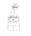
この実施形態のインバータ回路1は、バッテリ或いはDC―DCコンバータなどの直流電源2に接続された正側直流入力ライン3及び負側直流入力ライン4から直流電力を受け、これを交流電力に変換する回路である。このインバータ回路1は、複数相例えばU、V、Wの3相分の主ブリッジ5U、5V、5Wとこれら各主ブリッジとそれぞれ組みをなす補助ブリッジ6U、6V、6Wとからなる。これらブリッジ5U〜6Wを前記直流入力ライン3及び4間に接続する。U相の主ブリッジ5Uは2個のスイッチング素子7UPと7UNを直列に接続してなり、同様に主ブリッジ5Vは2個のスイッチング素子7VPと7VNとからなり、主ブリッジ5Wは2個のスイッチング素子7WPと7WNとからなる。各U相の補助ブリッジ6Uは2個のスイッチング素子8UPと8UNを直列に接続してなり、同様に補助ブリッジ6Vは2個のスイッチング素子8VPと8VNとからなり、補助ブリッジ6Wは2個のスイッチング素子8WPと8WNとからなる。
The inverter circuit 1 of this embodiment receives DC power from a positive
前記U相の主ブリッジ5Uの両スイッチング素子7UPと7UNとの共通接続点9Uと前記U相の補助ブリッジ6Uの両スイッチング素子8UPと8UNとの共通接続10Uとの間に限流リアクトル11Uを接続する。これと同様に他の各相についても共通接続点9Vと10Vとの間、及び9Wと10Wとの間に夫々限流リアクトル11V及び11Wを接続する。前記主ブリッジ5U、5V、5Wの前記共通接続点9U、9V、9Wはインバータ回路1の出力端子でもあり、これらに負荷としての回転電機例えばブラシレスモータ12の各ステータ巻線12U、12V、12Wを接続する。前記主ブリッジを構成する6個のスイッチング素子7UP〜7WN及び補助ブリッジを構成する6個のスイッチング素子8UP〜8WNは半導体スイッチング素子例えばFETからなり、夫々に還流ダイオードD1を逆向き並列に備えている。この還流ダイオードD1はFETに寄生する容量成分であってもよい。
A current-limiting
本実施形態のインバータ装置は制御部13を含み、この制御部13は前記12個のスイッチング素子7UP〜7WN並びに8UP〜8WNをオンオフ制御するスイッチング制御信号を出力する。この制御信号はこの種のインバータ装置で広く知られたPWM信号である。図中14は平滑用コンデンサである。
The inverter device of the present embodiment includes a
次に上記構成の作用を図2及び図3をも参照しながら述べる。インバータ回路1のUVW相の主ブリッジ5U、5V、5Wにおけるスイッチング素子7UP〜7WN、並びに補助ブリッジ6U、6V、6Wにおけるスイッチング素子8UP〜8WNのオンオフパターンは、制御部13でのPWM制御によって三相正弦波交流に変換する通常のインバータ回路のそれと同じである。これを図3によりU相について述べると、U相主ブリッジ6Uのスイッチング素子7UP及び7UNのオンオフパターンは図3の(b)(d)に示す通りであり、T1がいわゆるデットタイムである。
Next, the operation of the above configuration will be described with reference to FIGS. The ON / OFF patterns of the switching elements 7UP to 7WN in the UVW phase
本実施形態では、補助ブリッジのスイッチング素子のオンタイミングは、その補助ブリッジと組関係にある主ブリッジのスイッチング素子のオンタイミングに所定時間先行し、オフタイミングも主ブリッジのスイッチング素子のオフタイミングに先行する関係に定めてある。これを図3で説明すると、図3の(a)(b)に示すように主ブリッジ5Uの正側スイッチング素子7UPと補助ブリッジ6Uの正側スイッチング素子8UPの関係は、主ブリッジの素子7UPがオンする場合これより先行して時刻t1で補助ブリッジの素子8UPがオンする。また、(a)(b)を対比して解るように補助ブリッジの素子8UPのオフ動作は主ブリッジの素子7UPのオフ動作に先行する(時刻t2)。
In this embodiment, the on-timing of the switching element of the auxiliary bridge precedes the on-timing of the switching element of the main bridge that is paired with the auxiliary bridge by a predetermined time, and the off-timing also precedes the off-timing of the switching element of the main bridge. Stipulated in the relationship. This will be explained with reference to FIG. 3. As shown in FIGS. 3A and 3B, the relationship between the positive side switching element 7UP of the
このようなタイミング関係は、U相における主ブリッジ5Uの負側スイッチング素子7UNと補助ブリッジ6Uの負側スイッチング素子8UNの関係でも図3(c)(d)に示すように同様である。上記のようなオンオフパターンに基づく電流経路は図2に示すとおりであり、そのオンオフタイミング及び電流パターンは図3に示すとおりであり、直流‐交流変換の主体をなす主ブリッジ、一例としてU相の主ブリッジ5Uの次のようなスイッチングパターン(イ)(ロ)を柱に電流の流れを説明する。
Such a timing relationship is the same as shown in FIGS. 3C and 3D in the relationship between the negative side switching element 7UN of the
(イ)デットタイムT1内で主ブリッジ5Uの両スイッチング素子7UP、7UNが共にオフしている状態から正側スイッチング素子7UPがオン(時刻t2)→同素子オフ(t4)、(ロ)デットタイムT1内で主ブリッジ5Uの両スイッチング素子7UP、7UNが共にオフしている状態から負側スイッチング素子7UNがオン(時刻t6)→同素子オフ(時刻t8)のパターン。
(A) From the state where both switching elements 7UP and 7UN of the
(イ)のパターンでは、先ず先行する時刻t1で補助ブリッジ6Uの正側スイッチング素子8UPがオンする。すると経路L1で示すように、電流Iaが素子8UP及び限流リアクトル11Uを通り主ブリッジ5Uのオフ状態にある負側スイッチング素子7UNと逆向き並列な還流ダイオードD1を逆向きに通り負側直流入力ライン4に至る。このように還流ダイオードD1を逆向きに通る電流が発生するのは、前回のスイッチングサイクルでステータ巻線に保存された電気的エネルギーが還流電流として同ダイオードD1を順方向に通って生じた残留キャリアによるもので、いわゆるリカバリ電流である。
The pattern (a), first, the positive side switching elements 8 UP
このリカバリ電流の急激な立ち上がりは限流リアクトル11Uによって鈍化され、大きな短絡電流とはならない。この後、時刻t2で主ブリッジ5Uの正側スイッチング素子7UPがオンに転じ、主ブリッジ5Uによる通常のPWMスイッチング制御サイクルに移行する。先行してオンした補助ブリッジ6Uのスイッチング素子8UPは素子7UPのオン直後(時刻t3)にオフする。オンデューティの経過で正側スイッチング素子7UPがオフする(時刻t4)。
This rapid rise of the recovery current is slowed down by the current limiting
上記(イ)に続く(ロ)のパターンでは、主ブリッジ5Uの負側スイッチング素子7UNのオンに先行する時刻t5で補助ブリッジ6Uの負側スイッチング素子8UNがオンする。すると経路L2で示すように、電流Ibがオフ状態にある正側スイッチング素子7UPに逆向き並列な還流ダイオードD1を逆向きに通り、限流リアクトル11U、先行してオンされた上記スイッチング素子8UNを通り負側直流入力ライン4に至る。
In the pattern (b) following (b) above, the negative side switching element 8UN of the
ここでも、還流ダイオードD1を逆向きに流れる電流は、オフ状態にある正側スイッチング素子7UPと逆向き並列な還流ダイオードD1をステータ巻線からの還流電流が順方向に還流することに起因したリカバリ電流である。この場合もリカバリ電流の増大が限流リアクトル11Uによって抑制される。この後、時刻t6で主ブリッジ5Uの負側スイッチング素子7UNがオンに転じ、主ブリッジ5Uによる通常のPWMスイッチング制御サイクルに移行する。先行してオンした補助ブリッジ6Uのスイッチング素子8UNは素子7UNのオン直後(時刻t7)にオフする。
Again, the current flowing in the reverse direction through the freewheeling diode D1 is recovered due to the freewheeling current from the stator winding flowing in the forward direction through the freewheeling diode D1 in the reverse direction in parallel with the positive switching element 7UP in the off state. Current. Also in this case, an increase in the recovery current is suppressed by the current limiting
上記のようなリカバリ電流の通過によって限流リアクトル11Uに補助ブリッジ6Uのスイッチング素子8UPまたは8UNのオフによって電気的エネルギーが保存されるが、これは負荷であるステータ巻線12U〜12Wのどれかとこの時点でオンになっている主ブリッジ5Uのスイッチング素子と補助ブリッジ5Uのオフになっているスイッチング素子に逆向き並列な還流ダイオードD1を通る閉ループ中のステータ巻線内で電力として利用される。なお、図2及び図3において、電流IuはU相のステータ巻線電流、電流IUP及びIUNは夫々スイッチング素子7UP及び7UNを通過する電流である。
By passing the recovery current as described above, electrical energy is stored in the current limiting
この実施形態において、主及び補助ブリッジのスイッチング素子のオンオフタイミングは、補助ブリッジのそれを主ブリッジのそれに先行させる中で、補助ブリッジのスイッチング素子のオン期間をできるだけ短くすることがPWM制御の高速化にとって好ましい。その手段として、限流リアクトルの時定数を適宜設定することにより、補助ブリッジのスイッチング素子のオン期間を主ブリッジのスイッチング素子のPWM制御によるオンオフ周期より短くしたり、或いは、更に短くするため補助ブリッジのスイッチング素子のオフ時点を主ブリッジのスイッチング素子のオン時点の直後としたりしてもよい。 In this embodiment, the ON / OFF timing of the switching elements of the main and auxiliary bridges is such that the ON period of the switching elements of the auxiliary bridge is made as short as possible while the auxiliary bridge is preceded by that of the main bridge. Preferred for. As a means for this, by setting the time constant of the current-limiting reactor as appropriate, the auxiliary bridge switching element is turned on so that the on-period of the switching element of the auxiliary bridge is shorter than the on-off period by the PWM control of the switching element of the main bridge, or is further shortened. The switching element may be turned off immediately after the switching element of the main bridge is turned on.
以上のようにこの実施形態によれば、諸々の弊害をもたらすリカバリ電流を効果的に抑制することができると共に、補助ブリッジのオンオフタイミングを主ブリッジのそれに先行させるだけであるから制御の複雑化も招かず、また、限流リアクトルにリカバリ電流抑制時に保存された電気的エネルギーを電力として有効に活用できるインバータ装置を提供できる。 As described above, according to this embodiment, it is possible to effectively suppress the recovery current that causes various adverse effects, and also to make the control complicated because only the on / off timing of the auxiliary bridge precedes that of the main bridge. In addition, it is possible to provide an inverter device that can effectively use the electrical energy stored in the current-limiting reactor when the recovery current is suppressed as power.
Claims (2)
夫々ダイオードを逆向き並列に備えた一対のスイッチング素子を直列に接続してなる補助ブリッジと、
限流リアクトルと、
前記主ブリッジを構成する前記各スイッチング素子のオンオフ動作を制御する制御部とを備え、
前記主ブリッジと補助ブリッジとの組を1相分とする複数相分を前記正及び負側の直流入力ライン間に接続し、各相内における主ブリッジの両スイッチング素子の共通接続点と補助ブリッジの両スイッチング素子の共通接続点との間に前記限流リアクトルを接続し、
前記制御部は、前記補助ブリッジの正側及び負側のスイッチング素子のオン動作を夫々主ブリッジの正側及び負側のスイッチング素子のオン動作に先行して開始させ、
前記補助ブリッジの正側及び負側のスイッチング素子のオフ動作を夫々主ブリッジの正側及び負側のスイッチング素子のオン動作の直後に開始させる構成であることを特徴とするインバータ装置。 A main bridge formed by connecting in series a positive and negative DC input line and a pair of switching elements each having a diode in reverse parallel;
An auxiliary bridge formed by connecting a pair of switching elements each provided with a diode in reverse parallel and connected in series;
Current-limiting reactor ,
A control unit that controls the on / off operation of each of the switching elements constituting the main bridge ,
A plurality of phases corresponding to one set of the main bridge and auxiliary bridge are connected between the positive and negative DC input lines, and a common connection point of both switching elements of the main bridge and the auxiliary bridge in each phase said current limiting reactor connected between the common connection point of the both switching elements,
The control unit starts the ON operation of the positive side and negative side switching elements of the auxiliary bridge prior to the ON operation of the positive side and negative side switching elements of the main bridge, respectively.
An inverter device, characterized in that the off operation of the positive and negative switching elements of the auxiliary bridge is started immediately after the on operation of the positive and negative switching elements of the main bridge, respectively .
Priority Applications (4)
| Application Number | Priority Date | Filing Date | Title |
|---|---|---|---|
| JP2012119741A JP6021438B2 (en) | 2012-05-25 | 2012-05-25 | Inverter device |
| US13/795,181 US8787055B2 (en) | 2012-05-25 | 2013-03-12 | Inverter device |
| DE102013209557A DE102013209557A1 (en) | 2012-05-25 | 2013-05-23 | inverter device |
| CN201310197164.3A CN103427689B (en) | 2012-05-25 | 2013-05-24 | DC-to-AC converter |
Applications Claiming Priority (1)
| Application Number | Priority Date | Filing Date | Title |
|---|---|---|---|
| JP2012119741A JP6021438B2 (en) | 2012-05-25 | 2012-05-25 | Inverter device |
Publications (3)
| Publication Number | Publication Date |
|---|---|
| JP2013247767A JP2013247767A (en) | 2013-12-09 |
| JP2013247767A5 JP2013247767A5 (en) | 2015-05-28 |
| JP6021438B2 true JP6021438B2 (en) | 2016-11-09 |
Family
ID=49547203
Family Applications (1)
| Application Number | Title | Priority Date | Filing Date |
|---|---|---|---|
| JP2012119741A Expired - Fee Related JP6021438B2 (en) | 2012-05-25 | 2012-05-25 | Inverter device |
Country Status (4)
| Country | Link |
|---|---|
| US (1) | US8787055B2 (en) |
| JP (1) | JP6021438B2 (en) |
| CN (1) | CN103427689B (en) |
| DE (1) | DE102013209557A1 (en) |
Families Citing this family (6)
| Publication number | Priority date | Publication date | Assignee | Title |
|---|---|---|---|---|
| JP2014079150A (en) * | 2012-09-19 | 2014-05-01 | Toshiba Corp | Electromagnetic apparatus drive system and motor drive vehicle |
| WO2015194153A1 (en) * | 2014-06-18 | 2015-12-23 | 日本電気株式会社 | Switching output circuit |
| US10033325B2 (en) * | 2014-09-26 | 2018-07-24 | Mitsubishi Electric Corporation | Heat pump device, and air conditioner, heat pump water heater, refrigerator, and freezing machine that includes heat pump device |
| JP2016220421A (en) * | 2015-05-21 | 2016-12-22 | トヨタ自動車株式会社 | Non-contact power transmission device and power transmission system |
| US9612637B1 (en) * | 2015-11-25 | 2017-04-04 | Rockwell Automation Technologies, Inc. | System and method for controlling parallel legs in a switched mode power supply |
| JP6981212B2 (en) * | 2017-12-01 | 2021-12-15 | トヨタ自動車株式会社 | Contactless power transmission equipment and power transmission system |
Family Cites Families (9)
| Publication number | Priority date | Publication date | Assignee | Title |
|---|---|---|---|---|
| JPH05111263A (en) | 1991-10-15 | 1993-04-30 | Matsushita Electric Works Ltd | Power switching circuit |
| US5574636A (en) | 1994-09-09 | 1996-11-12 | Center For Innovative Technology | Zero-voltage-transition (ZVT) 3-phase PWM voltage link converters |
| JP3813859B2 (en) * | 2001-10-29 | 2006-08-23 | 東芝トランスポートエンジニアリング株式会社 | Power converter |
| JP2008067427A (en) * | 2006-09-05 | 2008-03-21 | Shindengen Electric Mfg Co Ltd | Power conversion device |
| EP2151915A1 (en) | 2007-05-29 | 2010-02-10 | Panasonic Corporation | Power converter |
| JP5095330B2 (en) * | 2007-09-20 | 2012-12-12 | 株式会社日立製作所 | Inverter device |
| JP5057238B2 (en) | 2008-05-12 | 2012-10-24 | 本田技研工業株式会社 | Resonant power converter |
| JP5111263B2 (en) | 2008-06-27 | 2013-01-09 | キヤノン株式会社 | Imaging apparatus and method |
| US8270191B2 (en) * | 2010-12-17 | 2012-09-18 | General Electric Company | Power generation system, power converter system, and methods of converting power |
-
2012
- 2012-05-25 JP JP2012119741A patent/JP6021438B2/en not_active Expired - Fee Related
-
2013
- 2013-03-12 US US13/795,181 patent/US8787055B2/en not_active Expired - Fee Related
- 2013-05-23 DE DE102013209557A patent/DE102013209557A1/en not_active Ceased
- 2013-05-24 CN CN201310197164.3A patent/CN103427689B/en not_active Expired - Fee Related
Also Published As
| Publication number | Publication date |
|---|---|
| DE102013209557A1 (en) | 2013-11-28 |
| US20130314965A1 (en) | 2013-11-28 |
| CN103427689B (en) | 2016-01-27 |
| JP2013247767A (en) | 2013-12-09 |
| US8787055B2 (en) | 2014-07-22 |
| CN103427689A (en) | 2013-12-04 |
Similar Documents
| Publication | Publication Date | Title |
|---|---|---|
| Koo et al. | Analysis and design of phase shift full bridge converter with series-connected two transformers | |
| EP2871760B1 (en) | Resistorless precharging | |
| JP5898848B2 (en) | Insulated power converter | |
| JP6021438B2 (en) | Inverter device | |
| US8466652B2 (en) | Method and apparatus for generating a charging circuit | |
| JP6206502B2 (en) | Power conversion device and power conversion method | |
| US9716455B2 (en) | Power conversion device and method of controlling the same | |
| US8587322B2 (en) | Methods and apparatus for motor emulation | |
| US9203323B2 (en) | Very high efficiency uninterruptible power supply | |
| US10439542B2 (en) | Electric power conversion device | |
| US9780586B2 (en) | Device and method for charging an electric energy store from a three-phase AC voltage source | |
| JP2010081786A (en) | Power switching circuit | |
| Afsharian et al. | A new PWM and commutation scheme for one phase loss operation of three-phase isolated buck matrix-type rectifier | |
| JPWO2007069314A1 (en) | Power converter | |
| JP6163768B2 (en) | Gate drive signal generator for multi-level power converter | |
| JP6467524B2 (en) | Power converter and railway vehicle | |
| WO2018123008A1 (en) | Converter device, motor driving apparatus, refrigerator, air conditioning apparatus, and heat pump water heater | |
| JP2009022060A (en) | Controller of ac electric motor | |
| JP6112747B2 (en) | Power supply | |
| JP2003230276A (en) | Control method for power converter | |
| JP2020178394A (en) | Converter circuit, power conversion system, and motor driving device | |
| JPS6323566A (en) | Method and apparatus for feeding electric power to dc source | |
| WO2018203422A1 (en) | Semiconductor element drive device and power conversion device | |
| JP6705234B2 (en) | Inverter control method | |
| JP2017017936A (en) | Device and system for power conversion |
Legal Events
| Date | Code | Title | Description |
|---|---|---|---|
| A521 | Written amendment |
Free format text: JAPANESE INTERMEDIATE CODE: A523 Effective date: 20150410 |
|
| A621 | Written request for application examination |
Free format text: JAPANESE INTERMEDIATE CODE: A621 Effective date: 20150410 |
|
| A131 | Notification of reasons for refusal |
Free format text: JAPANESE INTERMEDIATE CODE: A131 Effective date: 20160209 |
|
| A521 | Written amendment |
Free format text: JAPANESE INTERMEDIATE CODE: A523 Effective date: 20160408 |
|
| TRDD | Decision of grant or rejection written | ||
| A01 | Written decision to grant a patent or to grant a registration (utility model) |
Free format text: JAPANESE INTERMEDIATE CODE: A01 Effective date: 20160906 |
|
| A61 | First payment of annual fees (during grant procedure) |
Free format text: JAPANESE INTERMEDIATE CODE: A61 Effective date: 20161004 |
|
| R151 | Written notification of patent or utility model registration |
Ref document number: 6021438 Country of ref document: JP Free format text: JAPANESE INTERMEDIATE CODE: R151 |
|
| LAPS | Cancellation because of no payment of annual fees |