JP5977773B2 - Method of using composite magnetic parts and power supply system - Google Patents
Method of using composite magnetic parts and power supply system Download PDFInfo
- Publication number
- JP5977773B2 JP5977773B2 JP2014032985A JP2014032985A JP5977773B2 JP 5977773 B2 JP5977773 B2 JP 5977773B2 JP 2014032985 A JP2014032985 A JP 2014032985A JP 2014032985 A JP2014032985 A JP 2014032985A JP 5977773 B2 JP5977773 B2 JP 5977773B2
- Authority
- JP
- Japan
- Prior art keywords
- magnetic
- reactor
- current
- power supply
- power
- Prior art date
- Legal status (The legal status is an assumption and is not a legal conclusion. Google has not performed a legal analysis and makes no representation as to the accuracy of the status listed.)
- Active
Links
Images


Classifications
-
- H—ELECTRICITY
- H01—ELECTRIC ELEMENTS
- H01F—MAGNETS; INDUCTANCES; TRANSFORMERS; SELECTION OF MATERIALS FOR THEIR MAGNETIC PROPERTIES
- H01F27/00—Details of transformers or inductances, in general
- H01F27/28—Coils; Windings; Conductive connections
- H01F27/2823—Wires
-
- H—ELECTRICITY
- H01—ELECTRIC ELEMENTS
- H01F—MAGNETS; INDUCTANCES; TRANSFORMERS; SELECTION OF MATERIALS FOR THEIR MAGNETIC PROPERTIES
- H01F3/00—Cores, Yokes, or armatures
- H01F3/10—Composite arrangements of magnetic circuits
- H01F3/14—Constrictions; Gaps, e.g. air-gaps
-
- H—ELECTRICITY
- H01—ELECTRIC ELEMENTS
- H01F—MAGNETS; INDUCTANCES; TRANSFORMERS; SELECTION OF MATERIALS FOR THEIR MAGNETIC PROPERTIES
- H01F27/00—Details of transformers or inductances, in general
- H01F27/24—Magnetic cores
-
- H—ELECTRICITY
- H01—ELECTRIC ELEMENTS
- H01F—MAGNETS; INDUCTANCES; TRANSFORMERS; SELECTION OF MATERIALS FOR THEIR MAGNETIC PROPERTIES
- H01F27/00—Details of transformers or inductances, in general
- H01F27/34—Special means for preventing or reducing unwanted electric or magnetic effects, e.g. no-load losses, reactive currents, harmonics, oscillations, leakage fields
- H01F27/38—Auxiliary core members; Auxiliary coils or windings
-
- H—ELECTRICITY
- H01—ELECTRIC ELEMENTS
- H01F—MAGNETS; INDUCTANCES; TRANSFORMERS; SELECTION OF MATERIALS FOR THEIR MAGNETIC PROPERTIES
- H01F37/00—Fixed inductances not covered by group H01F17/00
-
- H—ELECTRICITY
- H01—ELECTRIC ELEMENTS
- H01F—MAGNETS; INDUCTANCES; TRANSFORMERS; SELECTION OF MATERIALS FOR THEIR MAGNETIC PROPERTIES
- H01F38/00—Adaptations of transformers or inductances for specific applications or functions
- H01F38/02—Adaptations of transformers or inductances for specific applications or functions for non-linear operation
- H01F38/023—Adaptations of transformers or inductances for specific applications or functions for non-linear operation of inductances
-
- H—ELECTRICITY
- H01—ELECTRIC ELEMENTS
- H01F—MAGNETS; INDUCTANCES; TRANSFORMERS; SELECTION OF MATERIALS FOR THEIR MAGNETIC PROPERTIES
- H01F38/00—Adaptations of transformers or inductances for specific applications or functions
- H01F38/14—Inductive couplings
-
- H—ELECTRICITY
- H02—GENERATION; CONVERSION OR DISTRIBUTION OF ELECTRIC POWER
- H02M—APPARATUS FOR CONVERSION BETWEEN AC AND AC, BETWEEN AC AND DC, OR BETWEEN DC AND DC, AND FOR USE WITH MAINS OR SIMILAR POWER SUPPLY SYSTEMS; CONVERSION OF DC OR AC INPUT POWER INTO SURGE OUTPUT POWER; CONTROL OR REGULATION THEREOF
- H02M3/00—Conversion of dc power input into dc power output
- H02M3/22—Conversion of dc power input into dc power output with intermediate conversion into ac
- H02M3/24—Conversion of dc power input into dc power output with intermediate conversion into ac by static converters
- H02M3/28—Conversion of dc power input into dc power output with intermediate conversion into ac by static converters using discharge tubes with control electrode or semiconductor devices with control electrode to produce the intermediate ac
- H02M3/325—Conversion of dc power input into dc power output with intermediate conversion into ac by static converters using discharge tubes with control electrode or semiconductor devices with control electrode to produce the intermediate ac using devices of a triode or a transistor type requiring continuous application of a control signal
- H02M3/335—Conversion of dc power input into dc power output with intermediate conversion into ac by static converters using discharge tubes with control electrode or semiconductor devices with control electrode to produce the intermediate ac using devices of a triode or a transistor type requiring continuous application of a control signal using semiconductor devices only
- H02M3/33569—Conversion of dc power input into dc power output with intermediate conversion into ac by static converters using discharge tubes with control electrode or semiconductor devices with control electrode to produce the intermediate ac using devices of a triode or a transistor type requiring continuous application of a control signal using semiconductor devices only having several active switching elements
- H02M3/33576—Conversion of dc power input into dc power output with intermediate conversion into ac by static converters using discharge tubes with control electrode or semiconductor devices with control electrode to produce the intermediate ac using devices of a triode or a transistor type requiring continuous application of a control signal using semiconductor devices only having several active switching elements having at least one active switching element at the secondary side of an isolation transformer
-
- H—ELECTRICITY
- H02—GENERATION; CONVERSION OR DISTRIBUTION OF ELECTRIC POWER
- H02M—APPARATUS FOR CONVERSION BETWEEN AC AND AC, BETWEEN AC AND DC, OR BETWEEN DC AND DC, AND FOR USE WITH MAINS OR SIMILAR POWER SUPPLY SYSTEMS; CONVERSION OF DC OR AC INPUT POWER INTO SURGE OUTPUT POWER; CONTROL OR REGULATION THEREOF
- H02M1/00—Details of apparatus for conversion
- H02M1/0067—Converter structures employing plural converter units, other than for parallel operation of the units on a single load
- H02M1/0074—Plural converter units whose inputs are connected in series
-
- H—ELECTRICITY
- H02—GENERATION; CONVERSION OR DISTRIBUTION OF ELECTRIC POWER
- H02M—APPARATUS FOR CONVERSION BETWEEN AC AND AC, BETWEEN AC AND DC, OR BETWEEN DC AND DC, AND FOR USE WITH MAINS OR SIMILAR POWER SUPPLY SYSTEMS; CONVERSION OF DC OR AC INPUT POWER INTO SURGE OUTPUT POWER; CONTROL OR REGULATION THEREOF
- H02M1/00—Details of apparatus for conversion
- H02M1/0067—Converter structures employing plural converter units, other than for parallel operation of the units on a single load
- H02M1/0077—Plural converter units whose outputs are connected in series
-
- H—ELECTRICITY
- H02—GENERATION; CONVERSION OR DISTRIBUTION OF ELECTRIC POWER
- H02M—APPARATUS FOR CONVERSION BETWEEN AC AND AC, BETWEEN AC AND DC, OR BETWEEN DC AND DC, AND FOR USE WITH MAINS OR SIMILAR POWER SUPPLY SYSTEMS; CONVERSION OF DC OR AC INPUT POWER INTO SURGE OUTPUT POWER; CONTROL OR REGULATION THEREOF
- H02M3/00—Conversion of dc power input into dc power output
- H02M3/02—Conversion of dc power input into dc power output without intermediate conversion into ac
- H02M3/04—Conversion of dc power input into dc power output without intermediate conversion into ac by static converters
- H02M3/10—Conversion of dc power input into dc power output without intermediate conversion into ac by static converters using discharge tubes with control electrode or semiconductor devices with control electrode
- H02M3/145—Conversion of dc power input into dc power output without intermediate conversion into ac by static converters using discharge tubes with control electrode or semiconductor devices with control electrode using devices of a triode or transistor type requiring continuous application of a control signal
- H02M3/155—Conversion of dc power input into dc power output without intermediate conversion into ac by static converters using discharge tubes with control electrode or semiconductor devices with control electrode using devices of a triode or transistor type requiring continuous application of a control signal using semiconductor devices only
- H02M3/156—Conversion of dc power input into dc power output without intermediate conversion into ac by static converters using discharge tubes with control electrode or semiconductor devices with control electrode using devices of a triode or transistor type requiring continuous application of a control signal using semiconductor devices only with automatic control of output voltage or current, e.g. switching regulators
- H02M3/158—Conversion of dc power input into dc power output without intermediate conversion into ac by static converters using discharge tubes with control electrode or semiconductor devices with control electrode using devices of a triode or transistor type requiring continuous application of a control signal using semiconductor devices only with automatic control of output voltage or current, e.g. switching regulators including plural semiconductor devices as final control devices for a single load
Landscapes
- Engineering & Computer Science (AREA)
- Power Engineering (AREA)
- Chemical & Material Sciences (AREA)
- Composite Materials (AREA)
- Physics & Mathematics (AREA)
- Nonlinear Science (AREA)
- Dc-Dc Converters (AREA)
- Coils Or Transformers For Communication (AREA)
Description
この発明は、可変磁気結合リアクトル、電源システム、および複合磁気部品の使用方法に関し、より特定的には、2個のリアクトル素子を一体化した可変磁気結合リアクトル、それを備えた電源システム、ならびに、2個のリアクトルの一体化構造を有する複合磁気部品の使用方法に関する。 The present invention relates to a variable magnetic coupling reactor, a power supply system, and a method of using a composite magnetic component, and more specifically, a variable magnetic coupling reactor in which two reactor elements are integrated, a power supply system including the variable magnetic coupling reactor, and The present invention relates to a method of using a composite magnetic component having an integrated structure of two reactors.
電力変換器に用いられるリアクトル等の誘導素子は、一般的に、磁性材料で構成されたコアにコイルを巻回することによって構成されるため大型化しやすい傾向にある。このため、磁性体(コア)を共通化することによって、複数の誘導素子を一体化した複合磁気部品を構成することが提案されている。 Inductive elements such as reactors used in power converters generally have a tendency to be large because they are formed by winding a coil around a core made of a magnetic material. For this reason, it has been proposed to form a composite magnetic component in which a plurality of inductive elements are integrated by sharing a magnetic body (core).
たとえば、特開2009−59995号公報(特許文献1)には、変圧器およびリアクトルを一体化した複合磁気部品の構成が記載される。特許文献1には、変圧器を構成する2つのコアの一方に一次巻線および二次巻線を巻回するとともに、他方のコアに一次巻線の延長部分を巻回する構成が記載されている。これにより、変圧器の一次巻線と直列に接続されるリアクトルを、上記延長部分によって変圧器と一体的に構成することができる。
For example, Japanese Patent Laying-Open No. 2009-59995 (Patent Document 1) describes a configuration of a composite magnetic component in which a transformer and a reactor are integrated.
また、特開2009−284647号公報(特許文献2)には、第1および第2のインダクタとトランスとを一体的に構成する複合型変圧器の構成が記載されている。 Japanese Patent Laying-Open No. 2009-284647 (Patent Document 2) describes the configuration of a composite transformer in which the first and second inductors and the transformer are integrally configured.
たとえば、2個の直流電源を含む電源システムにおいて、互いに独立に電流が制御され得る電流経路にそれぞれ含まれる2個のリアクトルを有する電力変換器の回路構成が存在する。このような回路構成では、一方のリアクトルを流れる電流によって生じた磁界が、他方のリアクトルに影響を及ぼす現象が発生し得る。特に、磁気結合によって、一方のリアクトルへの印加電圧が他方のリアクトルを流れる電流に影響を及ぼすような磁気的な干渉が、一体化された2つのリアクトル素子間に発生する可能性がある。 For example, in a power supply system including two DC power supplies, there is a circuit configuration of a power converter having two reactors each included in a current path in which currents can be controlled independently of each other. In such a circuit configuration, a phenomenon may occur in which a magnetic field generated by a current flowing through one reactor affects the other reactor. In particular, the magnetic coupling may cause magnetic interference between two integrated reactor elements such that the voltage applied to one reactor affects the current flowing through the other reactor.
この点について、特許文献1の複合磁気部品は、変圧器と単一のリアクトルを一体化するための技術であるから、2個のリアクトル素子を一体化する際の磁気的な干渉への対応については何ら開示していない。
About this point, since the composite magnetic part of
また、特許文献2に記載された複合型変圧器では、第1および第2のリアクトルを構成する第1および第2の巻線により生じる磁束がコア内では互いに干渉しないように、分割されたコアに離隔されて上記第1および第2の巻線が巻回される構成が特徴である。すなわち、特許文献2に記載された複合型変圧器は、一体的に構成された第1および第2のインダクタの間で磁気的な干渉が生じないように構成されている。
Further, in the composite transformer described in
この発明は上記のような問題点を解決するためになされたものであって、この発明の目的は、共通化されたコアを用いて一体的に構成された2個のリアクトル素子間の磁気的な干渉を積極的に利用した可変磁気結合リアクトルを構成することによって、リアクトルの小型軽量化を図ることである。 The present invention has been made to solve the above-described problems, and an object of the present invention is to provide a magnetic connection between two reactor elements that are integrally formed using a common core. It is intended to reduce the size and weight of the reactor by configuring a variable magnetic coupling reactor that positively utilizes such interference.
この発明のある局面では、可変磁気結合リアクトルは、第1の電流が通過するための第1および第2の巻線と、第2の電流が通過するための第3の巻線と、非線形磁性材料で構成されたコアとを備える。第1および第2の巻線は、電気的に直列接続される。コアは、第1の巻線が巻回される第1の磁脚部と、第2の巻線が巻回される第2の磁脚部と、第3の巻線が巻回される第3の磁脚部と、第1から第3の磁脚部の間に磁気経路を形成するための第4の磁脚部とを含むように構成される。第1および第2の巻線によって形成される第1のリアクトルと第3の巻線によって形成される第2のリアクトルとの動作状態は、第1および第2の電流の増加に応じて、第1および第2のリアクトルが磁気的に非干渉な状態で動作する非磁気結合モードから第1および第2のリアクトルが磁気的に干渉した状態で動作する磁気結合モードへ変化する。 In one aspect of the present invention, the variable magnetic coupling reactor includes first and second windings through which the first current passes, a third winding through which the second current passes, and non-linear magnetism. A core made of a material. The first and second windings are electrically connected in series. The core includes a first magnetic leg portion around which the first winding is wound, a second magnetic leg portion around which the second winding is wound, and a third winding around which the third winding is wound. 3 magnetic leg portions and a fourth magnetic leg portion for forming a magnetic path between the first to third magnetic leg portions. The operating states of the first reactor formed by the first and second windings and the second reactor formed by the third winding are in accordance with the increase in the first and second currents. The mode is changed from the nonmagnetic coupling mode in which the first and second reactors operate in a magnetically non-interfering state to the magnetic coupling mode in which the first and second reactors operate in a magnetically interfering state.
この発明の他の局面では、複合磁気部品の使用方法であって、複合磁気部品は、第1の電流が通過するための第1および第2の巻線と、第2の電流が通過するための第3の巻線と、非線形磁性材料で構成されたコアとを備える。第1および第2の巻線は、電気的に直列接続される。コアは、第1の巻線が巻回される第1の磁脚部と、第2の巻線が巻回される第2の磁脚部と、第3の巻線が巻回される第3の磁脚部と、第1から第3の磁脚部の間に磁気経路を形成するための第4の磁脚部とを含むように構成される。さらに、複合磁気部品は、第1および第2の巻線によって形成される第1のリアクトルと第3の巻線によって形成される第2のリアクトルとの動作状態が、第1および第2のリアクトルが磁気的に非干渉な状態で動作する非磁気結合モードから第1および第2のリアクトルが磁気的に干渉した状態で動作する磁気結合モードへ変化するように使用される。 In another aspect of the present invention, there is provided a method of using a composite magnetic component, wherein the composite magnetic component has a first and second windings through which a first current passes and a second current passes through. A third winding and a core made of a non-linear magnetic material. The first and second windings are electrically connected in series. The core includes a first magnetic leg portion around which the first winding is wound, a second magnetic leg portion around which the second winding is wound, and a third winding around which the third winding is wound. 3 magnetic leg portions and a fourth magnetic leg portion for forming a magnetic path between the first to third magnetic leg portions. Further, in the composite magnetic component, the operating states of the first reactor formed by the first and second windings and the second reactor formed by the third winding are the first and second reactors. Is used to change from a non-magnetic coupling mode that operates in a magnetically non-interfering state to a magnetic coupling mode in which the first and second reactors operate in a magnetically interfering state.
この発明のさらに他の局面では、電源システムは、第1の直流電源と、第2の直流電源と、第1および第2の直流電源と第1および第2の電力線との間で直流電力変換を実行するための電力変換器と、電力変換器の動作を制御するための制御装置とを備える。電力変換器は、第1および第2のリアクトルと、複数のスイッチング素子とを含む。第1および第2のリアクトルは、第1および第2の直流電源と第1および第2の電力線の間に形成される電力変換経路に含まれるように配置される。複数のスイッチング素子は、第1のリアクトルを通過する第1の電流と、第2のリアクトルを通過する第2の電流とを制御可能に配置される。第1および第2のリアクトルは、単一の複合磁気部品によって一体的に構成される。複合磁気部品は、第1の電流が通過するための第1および第2の巻線と、第2の電流が通過するための第3の巻線と、非線形磁性材料で構成されたコアとを備える。第1および第2の巻線は、電気的に直列接続される。コアは、第1の巻線が巻回される第1の磁脚部と、第2の巻線が巻回される第2の磁脚部と、第3の巻線が巻回される第3の磁脚部と、第1から第3の磁脚部の間に磁気経路を形成するための第4の磁脚部とを含むように構成される。第1および第2の巻線によって形成される第1のリアクトルと第3の巻線によって形成される第2のリアクトルとの動作状態は、第1および第2のリアクトルが磁気的に非干渉な状態で動作する非磁気結合モードから第1および第2のリアクトルが磁気的に干渉した状態で動作する磁気結合モードへ変化する。 In still another aspect of the present invention, a power supply system includes a first DC power supply, a second DC power supply, a DC power conversion between the first and second DC power supplies, and the first and second power lines. And a control device for controlling the operation of the power converter. The power converter includes first and second reactors and a plurality of switching elements. The first and second reactors are arranged so as to be included in a power conversion path formed between the first and second DC power supplies and the first and second power lines. The plurality of switching elements are disposed so as to be able to control a first current passing through the first reactor and a second current passing through the second reactor. The first and second reactors are integrally configured by a single composite magnetic component. The composite magnetic component includes first and second windings through which a first current passes, a third winding through which a second current passes, and a core made of a non-linear magnetic material. Prepare. The first and second windings are electrically connected in series. The core includes a first magnetic leg portion around which the first winding is wound, a second magnetic leg portion around which the second winding is wound, and a third winding around which the third winding is wound. 3 magnetic leg portions and a fourth magnetic leg portion for forming a magnetic path between the first to third magnetic leg portions. The operating states of the first reactor formed by the first and second windings and the second reactor formed by the third winding are such that the first and second reactors are magnetically non-interfering. The non-magnetic coupling mode operating in the state changes to the magnetic coupling mode operating in the state where the first and second reactors interfere magnetically.
好ましくは、可変磁気結合リアクトル、電源システムまたは、複合磁気部品の使用方法において、非磁気結合モードでは、第1および第2の磁脚部における透磁率が同等であるのに対して、磁気結合モードでは、第1および第2の磁脚部の一方での透磁率が、第1および第2の磁脚部の他方の透磁率よりも低い。 Preferably, in the method of using the variable magnetic coupling reactor, the power supply system, or the composite magnetic component, in the non-magnetic coupling mode, the magnetic permeability in the first and second magnetic legs is equal, while in the magnetic coupling mode Then, the permeability of one of the first and second magnetic leg portions is lower than the permeability of the other of the first and second magnetic leg portions.
さらに好ましくは、可変磁気結合リアクトル、電源システムまたは、複合磁気部品の使用方法において、非磁気結合モードでは、第1および第2の磁脚部の各々は、磁界の変化に対して磁束密度が線形に変化する線形領域で磁化される。一方、磁気結合モードでは、第1および第2の磁脚部の一方が非線形領域で磁化されるとともに他方が線形領域で磁化される。 More preferably, in the method of using the variable magnetic coupling reactor, the power supply system, or the composite magnetic component, in the non-magnetic coupling mode, each of the first and second magnetic legs has a linear magnetic flux density with respect to a change in the magnetic field. It is magnetized in a linear region that changes to. On the other hand, in the magnetic coupling mode, one of the first and second magnetic leg portions is magnetized in the nonlinear region and the other is magnetized in the linear region.
好ましくは、可変磁気結合リアクトル、電源システムまたは、複合磁気部品の使用方法において、第1の電流の通流によって第1の巻線および第2の巻線からそれぞれ発生される第1の磁界および第2の磁界と、第2の電流の通流によって第3の巻線から発生される第3の磁界とが、第1および第2の磁脚部の一方の磁脚部では強め合う一方で他方の磁脚部では弱め合い、かつ、第1および第2の磁界が第3の磁脚部では互いに弱め合うように、第1から第3の巻線は第1から第3の磁脚部にそれぞれ巻回される。 Preferably, in the method of using the variable magnetic coupling reactor, the power supply system, or the composite magnetic component, the first magnetic field and the second magnetic field generated from the first winding and the second winding, respectively, by the first current flow. The second magnetic field and the third magnetic field generated from the third winding by the second current flow strengthen each other in one of the first and second magnetic leg portions, while the other The first to third windings are connected to the first to third magnetic leg portions so that the first and second magnetic fields weaken each other and the first and second magnetic fields weaken each other in the third magnetic leg portion. Each is wound.
さらに好ましくは、可変磁気結合リアクトル、電源システムまたは、複合磁気部品の使用方法において、第1から第3の磁脚部は互いに同一方向に沿って形成される。第4の磁脚部は、第1から第3の磁脚部と交差する方向に沿って延在するように設けられる。さらに、第1および第2の巻線は、第1の磁界および第2の磁界が互いに逆方向に発生されるように第1および第2の磁脚部にそれぞれ巻回される。第3の巻線は、第3の磁界が第1または第2の磁界のいずれか一方と同じ方向に発生されるように第3の巻線に巻回される。 More preferably, in the method of using the variable magnetic coupling reactor, the power supply system, or the composite magnetic component, the first to third magnetic leg portions are formed along the same direction. The fourth magnetic leg portion is provided so as to extend along a direction intersecting with the first to third magnetic leg portions. Furthermore, the first and second windings are respectively wound around the first and second magnetic leg portions so that the first magnetic field and the second magnetic field are generated in opposite directions. The third winding is wound around the third winding such that the third magnetic field is generated in the same direction as either the first or second magnetic field.
あるいは、さらに好ましくは、可変磁気結合リアクトル、電源システムまたは、複合磁気部品の使用方法において、コアは、第4の磁脚部を構成する円環状の外径部位から円環の中心に向かって第1から第3の磁脚部が延在するとともに、当該中心において第1から第3の磁脚部が一体化される形状を有する。第1および第2の巻線は、第1の磁界および第2の磁界の一方が中心に向かって発生するとともに、第1および第2の磁界の他方が中心から遠ざかる方向に発生するように、第1および第2の磁脚部に巻回される。第3の巻線は、第3の磁界が第1または第2の磁界のいずれか一方と同じ方向に発生されるように第3の巻線に巻回される。 Alternatively, more preferably, in the method of using the variable magnetic coupling reactor, the power supply system, or the composite magnetic component, the core is arranged in a direction from the annular outer diameter portion constituting the fourth magnetic leg portion toward the center of the annular ring. The first to third magnetic leg portions extend and the first to third magnetic leg portions are integrated at the center. The first and second windings are generated such that one of the first magnetic field and the second magnetic field is generated toward the center, and the other of the first and second magnetic fields is generated in a direction away from the center. It is wound around the first and second magnetic leg portions. The third winding is wound around the third winding such that the third magnetic field is generated in the same direction as either the first or second magnetic field.
さらに好ましくは、可変磁気結合リアクトルの最大電流の通過時に、可変磁気結合リアクトル、電源システムまたは、複合磁気部品の使用方法において、第2の磁脚部における磁束密度が飽和磁束密度より小さく、かつ、第1の磁脚部における磁化方向が反転しないように、コアおよび第1から第3の巻線は構成される。 More preferably, in the method of using the variable magnetic coupling reactor, the power supply system, or the composite magnetic component when the maximum current of the variable magnetic coupling reactor passes, the magnetic flux density in the second magnetic leg portion is smaller than the saturation magnetic flux density, and The core and the first to third windings are configured so that the magnetization direction in the first magnetic leg portion is not reversed.
また好ましくは、可変磁気結合リアクトル、電源システムまたは、複合磁気部品の使用方法において、第1および第2の電流の位相は、第1および第2の電流の一方の電流の変曲点と、他方の電流の変曲点とが同一タイミングとなるように制御される。さらに好ましくは、第1および第2の電流の位相は、第1および第2の電流の極性が同じ場合には、第1および第2の電流の一方の電流の極大点と、他方の電流の極小点とが同一タイミングとなるように制御される。あるいは、第1および第2の電流の位相は、第1および第2の電流の極性が異なる場合には、第1および第2の電流の一方の電流の極大点と他方の電流の極大点とが同一タイミングとなるように、または、第1および第2の電流の一方の電流の極小点と他方の電流の極小点とが同一タイミングとなるように制御される。 Preferably, in the method of using the variable magnetic coupling reactor, the power supply system, or the composite magnetic component, the phase of the first and second currents is the inflection point of one of the first and second currents and the other The current inflection point is controlled so as to have the same timing. More preferably, when the first and second currents have the same polarity, the phase of the first and second currents is the maximum point of one of the first and second currents, and the other current is Control is performed so that the minimum point has the same timing. Alternatively, when the first and second currents have different polarities, the phases of the first and second currents are the maximum point of one of the first and second currents and the maximum point of the other current. Are controlled at the same timing, or the minimum point of one of the first and second currents and the minimum point of the other current are controlled at the same timing.
好ましくは、電源システムにおいて、電力変換器の複数のスイッチング素子は、第1から第4のスイッチング素子を有する。第1のスイッチング素子は、第1のノードおよび第1の電力線の間に電気的に接続される。第2のスイッチング素子は、第2のノードおおび第1のノードの間に電気的に接続される。第3のスイッチング素子は、第2の直流電源の負極端子と電気的に接続された第3のノードおよび第2のノードの間に電気的に接続される。第4のスイッチング素子は、第2の直流電源の負極端子と電気的に接続さ第2のノードおよび第2の電力線の間に電気的に、第1の直流電源と直列に接続される。第1のリアクトルは、第1の直流電源の正極端子と第2のノードとの間に電気的に接続される。第2のリアクトルは、第1および第3のノードの間に電気的に、第2の直流電源と直列に接続される。 Preferably, in the power supply system, the plurality of switching elements of the power converter include first to fourth switching elements. The first switching element is electrically connected between the first node and the first power line. The second switching element is electrically connected between the second node and the first node. The third switching element is electrically connected between the third node and the second node that are electrically connected to the negative terminal of the second DC power supply. The fourth switching element is electrically connected to the negative terminal of the second DC power supply, and is electrically connected in series with the first DC power supply between the second node and the second power line. The first reactor is electrically connected between the positive terminal of the first DC power source and the second node. The second reactor is electrically connected in series with the second DC power source between the first and third nodes.
この発明によれば、共通化されたコアを用いて一体的に構成された2個のリアクトル素子間の磁気的な干渉を積極的に利用した可変磁気結合リアクトルを構成することによって、リアクトルを小型軽量化できる。 According to the present invention, the reactor can be reduced in size by configuring the variable magnetic coupling reactor that positively utilizes magnetic interference between two reactor elements that are integrally configured using a common core. Weight can be reduced.
以下に、本発明の実施の形態について図面を参照して詳細に説明する。なお、以下では、図中の同一または相当部分には同一符号を付して、その説明は原則的に繰返さないものとする。 Embodiments of the present invention will be described below in detail with reference to the drawings. In the following, the same or corresponding parts in the drawings are denoted by the same reference numerals, and the description thereof will not be repeated in principle.
[実施の形態1]
図1は本発明の実施の形態に従う複合磁気部品(可変磁気結合リアクトル)が適用される電源システムの構成例を示す回路図である。
[Embodiment 1]
FIG. 1 is a circuit diagram showing a configuration example of a power supply system to which a composite magnetic component (variable magnetic coupling reactor) according to an embodiment of the present invention is applied.
図1を参照して、電源システム5は、直流電源B1と、電力変換器6と、直流電源B2と、電力変換器7とを備える。電源システム5は、直流電源B1,B2から負荷30への電力供給を制御する。あるいは、電源システム5は、負荷30によって発電された電力によって、直流電源B1,B2を充電する。
Referring to FIG. 1,
本実施の形態において、直流電源B1およびB2は、二次電池や電気二重層キャパシタ等の蓄電装置によって構成される。たとえば、直流電源B1は、リチウムイオン二次電池やニッケル水素電池のような二次電池で構成される。また、直流電源B2は、たとえば、電気二重層キャパシタやリチウムイオンキャパシタ等の出力特性に優れた直流電圧源要素により構成される。直流電源B1および直流電源B2は、「第1の直流電源」および「第2の直流電源」にそれぞれ対応する。ただし、直流電源B1およびB2を同種の蓄電装置によって構成することも可能である。 In the present embodiment, DC power supplies B1 and B2 are constituted by power storage devices such as secondary batteries and electric double layer capacitors. For example, DC power supply B1 is comprised with secondary batteries, such as a lithium ion secondary battery and a nickel metal hydride battery. The DC power source B2 is constituted by a DC voltage source element having excellent output characteristics such as an electric double layer capacitor and a lithium ion capacitor. The DC power supply B1 and the DC power supply B2 correspond to “first DC power supply” and “second DC power supply”, respectively. However, DC power supplies B1 and B2 can be configured by the same type of power storage device.
電力変換器6は、直流電源B1および負荷30の間に接続される。電力変換器7は直流電源B2および負荷30の間に接続される。電源システム5において、直流電源B1および20は、電力変換器6および7を介して、負荷30に対して並列に接続されていることが理解される。
負荷30は、電力変換器6,7からの出力電圧VHを受けて動作する。出力電圧VHの電圧指令値VH*は、負荷30の動作に適した電圧に設定される。電圧指令値は、負荷30の状態に応じて可変に設定されてもよい。さらに、負荷30は、回生発電等によって、直流電源B1,B2の充電電力を発生可能に構成されてもよい。たとえば、負荷30は、ハイブリッド自動車や電気自動車等の電動車両の走行用電動機および、当該電動機を駆動制御するためのインバータを含むように構成される。
The
電力変換器6は、直流電源B1と、負荷30と接続された電力線PLとの間で双方向のDC/DC変換を実行する。電力変換器7は、直流電源B2と電力線PLとの間で双方向のDC/DC変換を実行する。
The
電力変換器6および7の各々は、いわゆる昇圧チョッパ回路の構成を有する。具体的には、電力変換器6は、電力用半導体スイッチング素子(以下、単に「スイッチング素子」とも称する)Q1,Q2と、リアクトルL1とを有する。スイッチング素子Q1およびQ2は、電力線PLおよび電力線GLの間に直列に接続される。
Each of
リアクトルL1は、端子201および202を有する。端子201は、直流電源B1の正極端子と電気的に接続される。端子202は、スイッチング素子Q1およびQ2の接続ノードと電気的に接続される。これにより、リアクトルL1は、直流電源B1の正極端子と、スイッチング素子Q1およびQ2の接続ノードとの間に電気的に接続される。
Reactor L1 has
電力変換器7は、スイッチング素子Q3,Q4と、リアクトルL2とを有する。スイッチング素子Q3およびQ4は、電力線PLおよび電力線GLの間に直列に接続される。リアクトルL2は、端子203および204を有する。端子203は、直流電源B2の正極端子と電気的に接続される。端子204は、スイッチング素子Q3およびQ4の接続ノードと電気的に接続される。これにより、リアクトルL2は、直流電源B2の正極端子と、スイッチング素子Q3およびQ4の接続ノードとの間に電気的に接続される。
本実施の形態において、スイッチング素子としては、IGBT(Insulated Gate Bipolar Transistor)、電力用MOS(Metal Oxide Semiconductor)トランジスタ、あるいは電力用バイポーラトランジスタ等を用いることができる。スイッチング素子Q1〜Q4に対しては、逆並列ダイオードD1〜D4が配置されている。スイッチング素子Q1〜Q4は、制御装置40からの制御信号SG1〜SG4に応答して、オンオフを制御することが可能である。
In this embodiment, an IGBT (Insulated Gate Bipolar Transistor), a power MOS (Metal Oxide Semiconductor) transistor, a power bipolar transistor, or the like can be used as the switching element. Anti-parallel diodes D1 to D4 are arranged for switching elements Q1 to Q4. Switching elements Q1 to Q4 can control on / off in response to control signals SG1 to SG4 from
昇圧チョッパ回路によって構成される電力変換器6,7では、所定周期(スイッチング
周期)内での上アーム素子(Q1,Q3)と下アーム素子(Q2,Q4)とのオン期間比を示すデューティ比に応じて、DC出力が制御される。一般的には、デューティ比を示すDC信号と、所定周波数のキャリア信号との比較に応じて、上アーム素子および下アーム素子が相補にオンオフするように、スイッチング素子Q1〜Q4は制御される。
In
昇圧チョッパ回路における電圧変換比(昇圧比)は、低圧側(直流電源側)の電圧Vi、高圧側(負荷側)の電圧VH、および、下アーム素子のデューティ比DTを用いて、下記(1)式で示されることが知られている。なお、デューティ比DTは、下アーム素子のオン期間およびオフ期間の和であるスイッチング周期に対する、下アーム素子のオン期間比で定義される。なお、下アーム素子のオフ期間には、上アーム素子がオンされる。 The voltage conversion ratio (boost ratio) in the boost chopper circuit is expressed by the following (1) using the voltage Vi on the low voltage side (DC power supply side), the voltage VH on the high voltage side (load side), and the duty ratio DT of the lower arm element. It is known that The duty ratio DT is defined as the ratio of the on-period of the lower arm element to the switching cycle that is the sum of the on-period and off-period of the lower arm element. The upper arm element is turned on during the off period of the lower arm element.
VH=1/(1−DT)・Vi …(1)
制御装置40は、たとえば、図示しないCPU(Central Processing Unit)および
メモリを有する電子制御ユニット(ECU)によって構成される。制御装置40は、メモリに記憶されたマップおよびプログラムに基づいて、各センサによる検出値を用いた演算処理を行なうように構成される。あるいは、制御装置40の少なくとも一部は、電子回路等のハードウェアにより所定の数値・論理演算処理を実行するように構成されてもよい。
VH = 1 / (1-DT) · Vi (1)
The
制御装置40は、負荷30への出力電圧VHを制御するために、スイッチング素子Q1〜Q4のオンオフを制御する制御信号SG1〜SG4を生成する。なお、図1では図示を省略しているが、直流電源B1の電圧(V[1]と表記する)および電流(I[1]と表記する)、直流電源B2の電圧(V[2]と表記する)および電流(I[2]と表記する)、ならびに、出力電圧VHの検出器(電圧センサ,電流センサ)が設けられている。電力変換器6において、電流I[1]は、リアクトルL1を流れる電流IL1に相当する。同様に、電力変換器7において、電流I[2]は、リアクトルL2を流れる電流IL2に相当する。
以下では、直流電源B1,B2の放電時(電源システム5の力行動作時)における電流を正値(IL1>0,IL2>0)で表わす一方で、直流電源B1,B2の充電時(電源システム5の回生動作時)における電流を負値(IL1<0,IL2<0)で表わすこととする。 In the following, while the DC power supplies B1 and B2 are discharged (during powering operation of the power supply system 5), the currents are represented by positive values (IL1> 0, IL2> 0), while the DC power supplies B1 and B2 are charged (power supply system). The current at the time of the regenerative operation of 5 is represented by a negative value (IL1 <0, IL2 <0).
図2は、図1に示した電源システム5の一般的な制御ブロック図である。なお、以下では、図2を始めとする各ブロック図中の機能ブロックについて、制御装置40によるソフトウェア処理および/またはハードウェア処理によってその機能が実現されるものとする。
FIG. 2 is a general control block diagram of the
図2を参照して、電力変換器6,7で共通の制御(出力電圧VHの電圧制御)を同時に実行すると、回路が破綻する可能性がある。したがって、電力変換器6,7は、一方のバッテリが電圧源として動作する一方で、他方のバッテリが電流源として動作するように、直流電源B1,B2と負荷30との間でDC/DC変換を実行する。
Referring to FIG. 2, if common control (voltage control of output voltage VH) is simultaneously performed in
ここでは、直流電源B1が電流源として動作するように、電力変換器6は、バッテリ電流I[1]を電流指令値Ii*に従って制御するものとする。一方で、電力変換器7は、直流電源B2が電圧源として動作するように、出力電圧VHを電圧指令値VH*に従って制御する。
Here, it is assumed that
ここで、直流電源B1の電力P[1]、直流電源B2の電力P[2]、負荷30への出力電力Poおよび、電流源における電流指令値Ii*の間には、下記(2)式の関係が成立する。
Here, among the power P [1] of the DC power supply B1, the power P [2] of the DC power supply B2, the output power Po to the
P[2]=Po−P[1]=Po−V[1]・Ii* …(2)
直流電源B1の電圧V[1]の検出値に応じて、P[1]*=V[1]・Ii*が一定になるように電流指令値Ii*を設定すれば、電流源を構成する直流電源B1の電力P[1]を電力指令値P[1]*に制御できる。
P [2] = Po−P [1] = Po−V [1] · Ii * (2)
If the current command value Ii * is set so that P [1] * = V [1] · Ii * becomes constant according to the detected value of the voltage V [1] of the DC power supply B1, a current source is configured The power P [1] of the DC power supply B1 can be controlled to the power command value P [1] *.
なお、直流電源B2を電流源とし直流電源B1を電圧源として制御することも可能である。この場合には、電流源を構成する直流電源B2の電力P[2]について、V[2]・Ii*が一定になるように電流指令値Ii*を設定すれば、直流電源B2の電力P[2]
を電力指令値に従って制御できる。
It is also possible to control the DC power supply B2 as a current source and the DC power supply B1 as a voltage source. In this case, if the current command value Ii * is set so that V [2] · Ii * is constant for the power P [2] of the DC power source B2 constituting the current source, the power P of the DC power source B2 [2]
Can be controlled according to the power command value.
電流制御器41は、直流電源B1の電流I[1]が電流指令値Ii*と一致するように、電力変換器6のデューティ比を制御する。具体的には、電流偏差(Ii*−I[1])が正のときには、電流I[1]を上昇させるために、下アーム素子(Q2)のオン期間を長くするようにデューティ比が変化される。反対に、電流偏差(Ii*−I[1])が負のときには、電流I[1]を低下させるために、電力変換器6の上アーム素子(Q1)のオン期間が長くなるように、デューティ比が変化される。
The
電圧制御器42は、出力電圧VHが電圧指令値VH*と一致するように、電力変換器7のデューティ比を制御する。電圧制御器42は、電圧偏差(VH*−VH)が正のときには、出力電圧VHを上昇させるために、電力変換器7の下アーム素子(Q4)のオン期間比が長くなるようにデューティ比を変更する。反対に、電圧偏差(VH*−VH)が負のときには、出力電圧VHを低下させるために、電力変換器7の上アーム素子(Q3)のオン期間比が長くなるようにデューティ比を変更する。
The
このように、直流電源B1の出力は、電力変換器6によって電流指令値Ii*に従って電流制御される。一方で、直流電源B2の出力は、電力変換器7によって電圧指令値VH*に従って電圧制御される。なお、図2の例とは反対に、直流電源B1の出力を電力変換器6によって電圧指令値VH*に従って電圧制御する一方で、直流電源B2の出力を電力変換器7により電流指令値Ii*に従って電流制御することも可能である。
Thus, the output of the DC power supply B1 is current-controlled by the
図3には、図2に示した制御ブロックによって制御された電源システム5の動作波形例が示される。
FIG. 3 shows an example of operation waveforms of the
図3を参照して、P[1]>0かつP[2]>0であり、直流電源B1および20が放電して、負荷30へ電力を供給している場合の動作波形が示される。すなわち、Po=P[1]+P[2]で示される、出力電力Poは正である。 Referring to FIG. 3, operation waveforms are shown when P [1]> 0 and P [2]> 0, and DC power supplies B1 and B20 are discharged and power is supplied to load 30. That is, the output power Po indicated by Po = P [1] + P [2] is positive.
電力変換器6によって、直流電源B1の電流I[1]が電流指令値Ii*に従って一定に制御されるため、直流電源B1の電力P[1]も一定である。したがって、電圧指令値VH*が一定の下で負荷30の電力が増加する時刻t1〜t2の期間では、P[1]が一定に維持される一方で、直流電源B2の電力P[2]が増加する。
Since the
時刻t2〜t3の期間では、出力電力Poが減少するとともに、電圧指令値VH*が上昇する。電圧指令値VH*に従って電力変換器7によって出力電圧VHが上昇する。さらに、電力変換器6によって電流I[1]が一定に制御されるため電力P[1]が一定である一方で、電力P[2]は徐々に低下する。
In the period from time t2 to time t3, the output power Po decreases and the voltage command value VH * increases. The output voltage VH is increased by the
このように、電流制御される直流電源B1は、電流指令値Ii*に従って電力P[1]が制御される。一方で、直流電源B2は、出力電圧VHを確保しながら、負荷30への出力電力Poと直流電源B1の電力P[1]との差分を供給するためのバッファとして動作することになる。
In this way, the power P [1] is controlled in accordance with the current command value Ii * in the DC power source B1 that is current-controlled. On the other hand, the DC power supply B2 operates as a buffer for supplying a difference between the output power Po to the
上述のように、電源システム5では、電力変換器6のリアクトルL1を流れる電流IL1と、電力変換器7のリアクトルL2を流れる電流IL2とは独立に制御される。したがって、通常は、電流IL1によってリアクトルL2に誘起電圧が生じたり、反対に、電流IL2によってリアクトルL1に誘起電圧が生じたりすることを回避するように、すなわち、リアクトルL1およびL2の間が磁気的に非結合となるように、リアクトルL1およびL2は設計される。
As described above, in
まず比較例として、リアクトルL1,L2に間での磁気結合を確実に回避するために、リアクトルL1およびL2を独立した別個の磁気部品として構成した場合の構造について、図4を用いて説明する。 First, as a comparative example, a structure in the case where reactors L1 and L2 are configured as independent and separate magnetic components in order to reliably avoid magnetic coupling between reactors L1 and L2 will be described with reference to FIG.
図4を参照して、リアクトルL1を構成する磁気部品101は、コア110aおよび、コア110aに巻回された巻線120aによって構成される。コア110aには、ギャップ112aが設けられる。同様に、リアクトルL2を構成する磁気部品102は、コア110bおよび、コア110bに巻回された巻線120bによって構成される。コア110bには、ギャップ112bが設けられる。
Referring to FIG. 4,
リアクトルのインダクタンスLは、下記(3)式に従って、コイルの巻数NT、磁性材料の磁気抵抗Rおよびギャップの磁気抵抗rによって示される。 The inductance L of the reactor is represented by the number of turns NT of the coil, the magnetic resistance R of the magnetic material, and the magnetic resistance r of the gap according to the following equation (3).
L=NT・NT/(R+r) …(3)
磁気抵抗Rは、コア110a,110bの磁気特性(比透磁率)およびサイズ、形状(磁路長および断面積)によって調整できることが知られている。磁気抵抗rは、ギャップ112a,112bのギャップ長や個数によって調整することができる。
L = NT · NT / (R + r) (3)
It is known that the magnetic resistance R can be adjusted by the magnetic characteristics (relative magnetic permeability), size, and shape (magnetic path length and cross-sectional area) of the
また、コア110a,110bに用いられる磁性材料は非線形特性を有するため、過剰な磁束が発生すると、飽和現象のために特性が悪化する。このため、設計上の最大電流I(max)の通過時における最大磁束密度B(max)が、コアの飽和磁束密度を超えないように、コアの有効断面積SCを設計する必要がある。B(max)は、下記(4)式によって求められる。
Moreover, since the magnetic material used for the
B(max)=I(max)・N/(R+r)/SC …(4)
このように、リアクトルL1,L2を別個の磁気部品101,102で構成した場合には、誘起電圧の干渉を回避できるとともに、各磁器部品の設計によって、磁気飽和を避けて所望のインダクタンスを得ることができる。すなわち、インダクタンスの設計は比較的容易である。その一方で、コアが2個必要となるため、リアクトルL1,L2の大型化により、電力変換器6,7および電源システム5が大型化してしまう虞がある。
B (max) = I (max) · N / (R + r) / SC (4)
As described above, when the reactors L1 and L2 are constituted by the separate
本実施の形態では、リアクトルL1,L2について、共通コアを用いた複合磁気部品によって一体的に構成するとともに、両者間の磁気結合を積極的に利用することによって小型軽量化を図るためのメカニズムについて説明する。 In the present embodiment, the reactors L1 and L2 are configured integrally with a composite magnetic component using a common core, and a mechanism for reducing the size and weight by actively utilizing magnetic coupling between the two reactors. explain.
図5は、本発明の実施の形態1に従う可変磁気結合リアクトルの概略的な外観図の一例である。 FIG. 5 is an example of a schematic external view of the variable magnetic coupling reactor according to the first embodiment of the present invention.
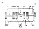
以下の説明で明らかになるように、本発明の実施の形態では、2個のリアクトルが一体的に構成された複合磁気部品が特定の使用態様で動作することによって、可変磁気結合リアクトルが構成される。以下では、当該複合磁気部品についても、可変磁気結合リアクトルと表記する。図5には、可変磁気結合リアクトル100の斜視図が示される。
As will be apparent from the following description, in the embodiment of the present invention, a variable magnetically coupled reactor is configured by operating a composite magnetic component in which two reactors are integrally configured in a specific usage mode. The Hereinafter, the composite magnetic component is also referred to as a variable magnetic coupling reactor. FIG. 5 shows a perspective view of the variable
図5を参照して、実施の形態1に従う可変磁気結合リアクトル100は、コア150と、巻線121a,121b,122とを含む。巻線121aおよび121bは、電気的に直列接続されて、リアクトルL1のコイルを構成する。巻線122は、リアクトルL2のコイルを構成する。図5から理解されるように、リアクトルL1を構成する巻線121a,121bと、リアクトルL2を構成する巻線122とは、共通のコア150の別個の部位にそれぞれ巻回されている。
Referring to FIG. 5, variable
図6は、図5に示した可変磁気結合リアクトル100の構造をさらに説明するための概念的な断面図である。
FIG. 6 is a conceptual cross-sectional view for further explaining the structure of variable
図6を参照して、コア150は、磁脚部151,152,153,154を有する。磁脚部151〜153には、ギャップ161〜163がそれぞれ設けられる。上述のように、ギャップ161〜163は、インダクタンスを調整する面で有用である。
Referring to FIG. 6,
巻線121aは、磁脚部151に巻回される。巻線121bは、磁脚部152に巻回される。巻線121aおよび121bは、端子201および202の間に電気的に直列接続される。したがって、リアクトルL1を流れるリアクトル電流IL1は、端子201から巻線121aおよび巻線121bを経由して端子202へ流れる。リアクトル電流IL1の通流により、巻線121aからは磁界211が発生され、巻線121bからは磁界212が発生される。
The winding 121a is wound around the
巻線122は、磁脚部153に巻回される。巻線122は、端子203および204の間に電気的に接続される。したがって、リアクトルL2を流れるリアクトル電流IL2は、端子203から巻線122を経由して端子204へ流れる。リアクトル電流IL2の通流により、巻線122によって磁界213が発生される。このように、磁脚部151〜153は、コア150における巻線121a,121b,122の巻回部位に相当する。一方で、磁脚部154は、コア150における巻線の非巻回部位に相当し、巻線が巻回された磁脚部151〜153の間に磁気経路を形成するように機能する。
The winding 122 is wound around the
巻線121aおよび121bは、共通のリアクトル電流IL1が巻線121aおよび121bを流れるときに、巻線121aにおける電流通流方向と、巻線121bにおける電流通流方向とは互いに逆となるように構成される。
巻線122は、リアクトル電流IL2がリアクトル電流IL1と同じ向きで流れたときに(たとえば、IL1>0かつIL2>0)、巻線121aおよび121bの一方と電流の向きが同じである一方で、他方とは電流の向きが逆となる。以下では、巻線121aおよび122の間で電流通流方向が同じとなる例を示す。すなわち、巻線121aは「第1の巻線」に対応し、巻線121bは「第2の巻線」に対応する。巻線122は、「第3の巻線」に対応する。
Winding 122 has the same current direction as one of
図7は、図6に示した各巻線の巻回態様の一例を説明するための概念図である。図7は、図5および図6に示した可変磁気結合リアクトル100の上面図に相当する。
FIG. 7 is a conceptual diagram for explaining an example of a winding mode of each winding shown in FIG. FIG. 7 corresponds to a top view of the variable
図7を参照して、端子201および202の間にリアクトル電流IL1が流される。導線121cによって、巻線121aおよび121bの間は、電気的に直列接続される。この際に、導線121cは、巻線121aおよび121bによって構成されるコイルにおける電流の向きが反対となるように、巻線121aおよび121bの間に接続される。
Referring to FIG. 7, reactor current IL <b> 1 flows between
この結果、図7に示されるように、巻線121aによって生じる磁界211は、コア上面側(図6中の上側)をN極とし、コア下面側(図6中の下側)をS極とする方向を有する。一方で、巻線121bによって生じる磁界212は、コア上面側(図6中の上側)をS極とし、コア下面側(図6中の下側)をN極とする方向を有する。すなわち、リアクトル電流IL1の通流によって、巻線121a,121bからそれぞれ発生される磁界211,212は、互いに反対方向である。
As a result, as shown in FIG. 7, the
さらに、端子203および204の間に、リアクトル電流IL1と同じ向きにリアクトル電流IL2が流される(たとえば、IL1>0,IL2>0)。これにより、巻線122からは磁界213が発生される。磁界213は、コア上面側(図6中の上側)をN極とし、コア下面側(図6中の下側)をS極とする方向を有する。すなわち、同一方向のリアクトル電流IL1,IL2によって、巻線122が生じる磁界213は、巻線121aが生じる磁界211とは同じ方向である一方で、巻線121bが生じる磁界212とは逆の方向である。
Furthermore, reactor current IL2 is allowed to flow between
図8は、図6に示した各巻線の巻回態様の他の例を説明するための概念図である。
図8に示した例では、端子204および導線121cが、図7とは異なる位置に設けられる。図8では、各巻線121a,121b,122での電流の向き、すなわち、磁界211〜213の方向を図7と同様にした上で、各巻線121a,121b,122の巻数(ターン数)が厳密に同一とされている。逆にいうと図7の構成では、巻線121a,121bの巻数が、巻線122よりも1/4ターンだけ多くなっている。
FIG. 8 is a conceptual diagram for explaining another example of the winding mode of each winding shown in FIG.
In the example shown in FIG. 8, the terminal 204 and the
図9は、実施の形態1に従う可変磁気結合リアクトル100の電気的な等価回路図である。
FIG. 9 is an electrical equivalent circuit diagram of variable
図9を参照して、端子201および202間に直列接続された巻線121aおよび121bは、リアクトルL1を構成する。電圧源11は、端子201,202間にリアクトル電圧VL1を印加する。たとえば、電圧源11は、電力変換器6のスイッチング素子Q1,Q2のオンオフ制御によって、パルス状にリアクトル電圧VL1を発生するように構成される。具体的には、図1の電力変換器6において、スイッチング素子Q2のオン期間において、VL1=V[1]となる(VL1>0)。一方で、スイッチング素子Q2のオフ期間(スイッチング素子Q1のオン期間)においては、V[1]−VL1=VHが成立するので、VL1=V[1]−VHとなる(VL1<0)。
Referring to FIG. 9,
同様に、端子203および204間に接続された巻線122は、リアクトルL2を構成する。電圧源12は、端子203,204間にリアクトル電圧VL2を印加する。たとえば、電圧源12は、電力変換器7のスイッチング素子Q3,Q4のオンオフ制御によって、パルス状にリアクトル電圧VL2を発生するように構成される。具体的には、図1の電力変換器7において、スイッチング素子Q4のオン期間には、VL2=V[2]となる(VL2>0)。一方で、スイッチング素子Q4のオフ期間(スイッチング素子Q3のオン期間)においては、V[2]−VL2=VHが成立するので、VL2=V[2]−VHとなる(VL2<0)。
Similarly, winding 122 connected between
ここで、巻線121a,121bおよび122は、図6に示されたように、磁脚部151〜153が一体的に構成された共通のコア150に巻回されている。したがって、巻線121a,121b,122で発生した磁束は、互いに干渉し合うことになる。
Here, as shown in FIG. 6, the
次に、図10および図11を用いてコア内部における各巻線からの発生磁束の関係について説明する。 Next, the relationship of the magnetic flux generated from each winding in the core will be described with reference to FIGS. 10 and 11.
図10および図11には、図6と同様の概念的な断面図が示される。図10には、リアクトルL1がコア内に発生する磁束が示される一方で、図11には、リアクトルL2がコア内に発生する磁束が示される。 10 and 11 are conceptual cross-sectional views similar to FIG. FIG. 10 shows the magnetic flux generated by reactor L1 in the core, while FIG. 11 shows the magnetic flux generated by reactor L2 in the core.
図10を参照して、磁脚部151に巻回された巻線121aから発生される磁界211による磁束221は、磁脚部154を経由して、磁脚部152および153にも作用する。同様に、磁脚部152に巻回された巻線121bから発生される磁界212による磁束222は、磁脚部154を経由して、磁脚部151および153にも作用する。磁界211および磁界212は、コア150内で、磁脚部151,152を含む一巡経路を形成する。
Referring to FIG. 10,
磁脚部151および152の各々において、磁界211および212による磁束221および222は同一方向に作用する。すなわち、磁界211および212は、磁脚部151および152の各々において、互いに強め合う。
In each of the
一方、磁脚部153において、磁界211および212による磁束221および222は反対方向に作用する。すなわち、磁界211および212は、磁脚部153において、互いに弱め合う。
On the other hand, in the
図11を参照して、磁脚部153に巻回された巻線122から発生される磁界213による磁束223は、磁脚部154を経由して、磁脚部151および152にも作用する。
Referring to FIG. 11, the
図10および図11を総合すると、リアクトルL2に対応する磁脚部153では、巻線121aからの磁束221と巻線121bからの磁束222とが打ち消し合う一方で、巻線122による磁束223が通過する。すなわち、磁脚部153での磁界の大きさは、リアクトル電流IL2によって生じる磁界213相当である。
10 and 11, in the
これに対して、リアクトルL1に対応する磁脚部151および152の間では、リアクトルL2からの磁束との干渉によって、磁界の大きさが不均衡になる。磁脚部152では、磁界211および212による磁束221,222と、磁界213による磁束223(図11)とは同じ方向であるので、磁界211および212と磁界213とは強め合う。これに対して、磁脚部151では、磁界211および212による磁束221,222と、磁界213による磁束223(図11)とは反対方向であるので、磁界211および212と磁界213とは弱め合う。磁脚部151は「第1の磁脚部」に対応し、磁脚部152は「第2の磁脚部」に対応する。また、磁脚部153は「第3の磁脚部」に対応する。
On the other hand, between the
このように、本実施の形態の可変磁気結合リアクトル100では、リアクトルL1を形成する巻線121a,121bが巻回された磁脚部151および152の一方(本実施例では磁脚部152)において、リアクトル電流IL1およびIL2のそれぞれによる磁界が互いに強め合う。一方で、他方の磁脚部(本実施例では磁脚部151)では、リアクトル電流IL1およびIL2による磁界が打ち消し合う。このような相互磁化作用によって、リアクトル電流IL1およびIL2が流れている下で、磁脚部151および152の間で、磁界の大きさが不均衡となる。
Thus, in the variable
(可変磁気飽和回路における動作原理式)
次に、本実施の形態に従う可変磁気結合リアクトル100における上述の磁界相互作用を解析するために、可変磁気結合リアクトル100の動作原理式について説明する。
(Operating principle formula in variable magnetic saturation circuit)
Next, in order to analyze the above-described magnetic field interaction in the variable
図12は、コア150の形状パラメータを説明するための斜視図である。さらに、図13には、図12に示されたコア150における磁気的な等価回路図が示される。
FIG. 12 is a perspective view for explaining the shape parameters of the
図12を参照して、コア150は、たとえば、矩形形状の組合せで構成される。すなわち、幅W×奥行きDの上下基底部の間に、高さHGの磁脚部151〜153が、互いに同一方向に沿って柱状に形成されている。磁脚部154は、磁脚部151〜153と交差する方向に延在するように設けられる。磁脚部154は、磁脚部151〜153の一端側同士、および、他端側同士をそれぞれ接続するように形成される。
Referring to FIG. 12 ,
磁脚部151〜153は、断面積SC1〜SC3をそれぞれ有する。また、磁脚部151〜153の幅は、それぞれW1〜W3である。さらに、磁脚部151〜153に設けられたギャップ161〜163は、ギャップ長Lg1〜Lg3をそれぞれ有する。さらに、磁脚部151〜153によってそれぞれ形成される磁気回路251〜253の磁路長を、それぞれLN1〜LN3とする。なお、磁脚部151および152は同一形状で形成される。すなわち、Lg1=Lg2、かつ、SC1=SC2(W1=W2)である。
The
図12に示された形状パラメータ値を用いると、磁脚部151〜153の断面積SC1〜SC3は(5),(6)式で示される。また、磁路長LN1〜LN3は、下記式(7),(8)で示される。
When the shape parameter values shown in FIG. 12 are used, the cross-sectional areas SC1 to SC3 of the

次に図13を参照して、磁脚部151による磁気回路251では、直列接続された磁路長LN1の磁気抵抗Rmaおよびギャップ長Lg1の磁気抵抗Rgaを、磁束φ1が通過する。同様に、磁脚部152による磁気回路252では、直列接続された磁路長LN2の磁気抵抗Rmbおよびギャップ長Lg2の磁気抵抗Rgbを、磁束φ2が通過する。また、磁脚部153による磁気回路253では、直列接続された磁路長LN3の磁気抵抗Rmcおよびギャップ長Lg3の磁気抵抗Rgcを、磁束φ3が通過する。図10に示された磁界方向から理解されるとおり、ループを形成する磁束φ1およびφ2について、磁気回路251および252のそれぞれにおける方向は互いに逆である。
Next, referring to FIG. 13 , in the
図13の磁気抵抗Rma,Rmb,Rmcは、下記式(9)〜(11)式で示される。また、ギャップ部分の磁気抵抗Rga,Rgb,Rgcは、下記式(12),(13)で示される。 The magnetic resistances Rma, Rmb, and Rmc in FIG. 13 are expressed by the following formulas (9) to (11). Further, the magnetic resistances Rga, Rgb, and Rgc of the gap portion are expressed by the following formulas (12) and (13).
式(9)〜(13)において、μ0は真空中の透磁率を示し、μr1〜μr3は、磁脚部151〜153(磁気回路251〜253)における比透磁率を示す。磁脚部151,152,153(磁気回路251,252,253)における透磁率は、それぞれμ0・μr1,μ0・μr2,μ0・μr3となる。
In Expressions (9) to (13), μ0 represents the magnetic permeability in vacuum, and μr1 to μr3 represent the relative magnetic permeability in the
後程説明するように、比透磁率の特性は、コア150の材質に依存する。また、コア150の磁化特性が非線形性を有する場合には、比透磁率はμr1〜μr3、磁界の大きさ(磁束密度)にも依存して変化する。一方で、L1〜L3、SC1〜SC3およびLg1〜Lg3は、図12に示されたコア形状に依存する固定値である。したがって、磁気抵抗Rga〜Rgcは、磁脚部151,152,153における透磁率μ0・μr1,μ0・μr2,μ0・μr3の関数として変化し得る。
As will be described later, the characteristic of the relative permeability depends on the material of the
磁気回路251〜253の磁気抵抗R1〜R3は、下記の式(14)〜(16)によって示される。また、以降での表記を簡略化するために、式(17)に示されるように、磁気抵抗R1〜R3に基づくパラメータRkが導入される。
The magnetic resistances R1 to R3 of the
上記より、磁気抵抗R1〜R3およびパラメータRkは、比透磁率μr1〜μr3に依存した変数となり得る。 From the above, the magnetic resistances R1 to R3 and the parameter Rk can be variables depending on the relative magnetic permeability μr1 to μr3.
本実施の形態に従う可変磁気結合リアクトル100のインダクタンスを求めるために、巻線121a,121b,122によるインダクタンスを算出する。各インダクタンスは、各巻線による自己インダクタンスと、巻線間の相互インダクタンスとの和によって求められる。
In order to obtain the inductance of variable
巻線121a,121b,122のそれぞれ自己インダクタンスLa,Lb,Lcは、式(15)〜(17)のパラメータを用いて、下記(18)〜(20)で示される。以下では、巻線121aおよび121b,122の巻数の和をNT1とし、巻線122の巻数をNT3とする。
The self-inductances La, Lb, and Lc of the
また、相互インダクタンスについては、式(15)〜(17)のパラメータを用いて、下記(21)〜(23)で示される。式(21)には、巻線121aおよび121bの間の相互インダクタンスMab,Mbaが示される。式(22)には、巻線121bおよび122の間の相互インダクタンスMbc,Mcbが示される。式(23)には、巻線122および121aの間の相互インダクタンスMca,Macが示される。
The mutual inductance is expressed by the following (21) to (23) using the parameters of the equations (15) to (17). Equation (21) shows the mutual inductances Mab and Mba between the
再び図13を参照して、磁気回路251には誘起電圧Vaが生じ、磁気回路252には誘起電圧Vbが生じ、磁気回路253には誘起電圧Vcが生じる。図10および図11に示した電流方向から、誘起電圧VaおよびVbは同一方向であり、かつ、誘起電圧Vcは、誘起電圧VaおよびVbと逆方向である。
Referring to FIG. 13 again, an induced voltage Va is generated in the
磁気回路251および252での誘起電圧VaおよびVbの和は、上述したリアクトルL1に印加される電圧VL1と釣り合う。同様に、磁気回路253での誘起電圧Vcは、リアクトルL2の電圧VL2と釣り合う。
The sum of the induced voltages Va and Vb in the
次に、上記式(18)〜(20)を用いて、リアクトルL1,L2に印加される電圧Vx,Vyと流れる電流ix,iyとの関係式として、式(24),(25)が求められる。電圧VxおよびVyは、リアクトル電圧VL1およびVL2に相当し、電流ixおよびiyは、リアクトル電流IL1およびIL2に相当する。 Next, using the above equations (18) to (20), equations (24) and (25) are obtained as relational expressions between the voltages Vx and Vy applied to the reactors L1 and L2 and the flowing currents ix and iy. It is done. Voltages Vx and Vy correspond to reactor voltages VL1 and VL2, and currents ix and iy correspond to reactor currents IL1 and IL2.
式(24)および(25)を、電流変化dix/dtおよびdiy/dtについて解き直すように変形すると、下記式(26),(27)が得られる。 When the equations (24) and (25) are modified so as to be solved for the current changes dix / dt and diy / dt, the following equations (26) and (27) are obtained.
ここで、式(26),(27)中で用いられた各パラメータLc,(Mbc−Mcb),DET,(La+Lb+Mab)は、下記の式(28)〜(31)で表わすことができる。 Here, the parameters Lc, (Mbc−Mcb), DET, and (La + Lb + Mab) used in the equations (26) and (27) can be expressed by the following equations (28) to (31).
式(28)〜(31)を式(26),(27)に代入すると、下記の式(32)が得られる。 Substituting Equations (28) to (31) into Equations (26) and (27) yields the following Equation (32).
ここで、解析を簡素化するために、リアクトルL1およびL2の巻線数が等しい、すなわち、NT1=NT3とすると、式(32)は、下記の式(33)に変形される。 Here, in order to simplify the analysis, assuming that the number of windings of reactors L1 and L2 is equal, that is, NT1 = NT3, equation (32) is transformed into equation (33) below.
式(33)から理解されるように、R1=R2のとき、すなわち、磁脚部151および152のそれぞれによる磁気回路251および252の磁気抵抗R1およびR2が同等であるとき、リアクトル電流IL1の電流変化率に相当する(dix/dt)は、リアクトルL2の電圧Vyの影響を受けることなく、リアクトルL1のVxによって決まる。同様に、リアクトル電流IL2の電流変化率に相当する(diy/dt)は、リアクトルL1の電圧Vxの影響を受けることなく、リアクトルL2の電圧Vyに応じて決まる。すなわち、リアクトルL1およびL2の間に磁気結合は生じず、リアクトルL1およびL2は、磁気的に非干渉な状態で動作する(非磁気結合モード)。
As understood from the equation (33), when R1 = R2, that is, when the magnetic resistances R1 and R2 of the
これに対して、磁気抵抗R1およびR2の間に差が生じると、R2−R1≠0となることにより、リアクトルL1の電圧Vxが電流変化率(diy/dt)に影響するとともに、リアクトルL2の電圧Vxが電流変化率(dix/dt)に影響するようになる。すなわち、リアクトルL1およびL2の間に磁気結合が発生して、両者が磁気的に相互干渉するようになる(磁気結合モード)。この結果、リアクトルL1,L2の電圧−電流挙動が変化することになる。なお、インダクタンスを表現するために、式(24),(25)におけるMbc−McaをMxyと置くと、式(24),式(25)は、式(34)で示すことができる。 On the other hand, when a difference occurs between the magnetic resistances R1 and R2, R2−R1 ≠ 0, so that the voltage Vx of the reactor L1 affects the current change rate (diy / dt) and the reactor L2 The voltage Vx affects the current change rate (dix / dt). That is, magnetic coupling occurs between reactors L1 and L2, and both magnetically interfere with each other (magnetic coupling mode). As a result, the voltage-current behavior of reactors L1 and L2 changes. In order to express inductance, when Mbc-Mca in the equations (24) and (25) is set as Mxy, the equations (24) and (25) can be expressed by the equation (34).
式(34)において、Mxyは、上述の磁気結合による相互干渉項に相当する。すなわち、磁気結合が発生しない場合には、Mxy=0である。このとき、リアクトルL1のインダクタンスは、巻線121a,121bによるインダクタンスの合計値である、La+Lb+2・Mabに相当する。また、リアクトルL2のインダクタンスは、巻線122によるインダクタンスLcに相当する。
In Expression (34), Mxy corresponds to the mutual interference term due to the magnetic coupling described above. That is, when no magnetic coupling occurs, Mxy = 0. At this time, the inductance of the reactor L1 corresponds to La + Lb + 2 · Mab, which is the total value of the inductances of the
一方で、インダクタンスL1,L2間に、磁気抵抗R1およびR2の差に起因した磁気干渉が発生すると、Mxy≠0となって、リアクトルL1およびL2の各インダクタンスが、Mxy=0(磁気的に非結合)のときから変化することになる。 On the other hand, when magnetic interference due to the difference between the magnetic resistances R1 and R2 occurs between the inductances L1 and L2, Mxy ≠ 0, and the inductances of the reactors L1 and L2 become Mxy = 0 (magnetically non-magnetic). It will change from the time of connection.
ここで、上述のように、磁気抵抗R1,R2は、磁脚部151,152の透磁率(比透磁率)に応じて変化する。したがって、磁脚部151,152の透磁率(比透磁率)に差が生じると、磁気抵抗R1およびR2に差が生じることが理解される。
Here, as described above, the magnetic resistances R1 and R2 change according to the magnetic permeability (relative magnetic permeability) of the
さらに、図10および図11で説明したように、本実施の形態に従う可変磁気結合リアクトルでは、リアクトルL1に対応する磁脚部151および152の間では、リアクトルL2からの磁束との作用によって、磁界の大きさが不均衡になる。したがって、このような磁界の不均衡に起因して透磁率(比透磁率)に差が生じると、R1≠R2となって磁気結合による磁気的な干渉が発生することになる。
Further, as described in FIGS. 10 and 11, in the variable magnetic coupling reactor according to the present embodiment, a magnetic field is generated between
ここで、磁界および磁束密度と透磁率の関係について図14および図15を用いて説明する。 Here, the relationship between the magnetic field, the magnetic flux density, and the magnetic permeability will be described with reference to FIGS.
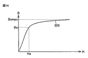
図14には、強磁性体の一般的な磁化曲線(B−H曲線)が示される。図14には、磁界が印加されていない状態から磁化されるときの磁化曲線305(いわゆる、初期磁化曲線)が示される。 FIG. 14 shows a general magnetization curve (BH curve) of a ferromagnetic material. FIG. 14 shows a magnetization curve 305 (so-called initial magnetization curve) when magnetized from a state where no magnetic field is applied.
図14を参照して、磁界Hが大きくなるに従って磁束密度Bが増加する。しかしながら、磁界Hが大きくなっていくと、磁束密度Bの増加の割合は徐々に減少する。そして、最終的には、B−H曲線が水平となる、すなわち、磁界を大きくしても磁束密度がこれ以上増加しない、磁気飽和と呼ばれる現象が発生する。磁気飽和時の磁束密度は、飽和磁束密度Bsmaxと称される。 Referring to FIG. 14, the magnetic flux density B increases as the magnetic field H increases. However, as the magnetic field H increases, the rate of increase of the magnetic flux density B gradually decreases. Eventually, the BH curve becomes horizontal, that is, a phenomenon called magnetic saturation occurs in which the magnetic flux density does not increase any more even when the magnetic field is increased. The magnetic flux density at the time of magnetic saturation is called saturation magnetic flux density Bsmax.
図14に示された、磁化曲線(B−H曲線)における接線の傾きが、磁性体(コア150)の透磁率に相当する。 The slope of the tangent in the magnetization curve (BH curve) shown in FIG. 14 corresponds to the magnetic permeability of the magnetic body (core 150).
図15には、図14に示された磁化曲線における磁束密度の変化に対する透磁率の変化特性が示される。 FIG. 15 shows the change characteristic of the magnetic permeability with respect to the change of the magnetic flux density in the magnetization curve shown in FIG.
図15を参照して、磁界H<Ha、すなわち磁束密度B<Baの領域310では、磁界Hの変化に対して、磁束密度Bはほぼ線形に変化する。領域310では、透磁率μはほぼ一定値となる。このような領域を、以下では「線形領域310」とも称する。
Referring to FIG. 15, in
これに対して、H>Ha、すなわち、B>Baの領域では、磁界Hの増加に対する磁束密度Bの増加率、すなわち、透磁率μが線形領域310よりも低くなる。また、透磁率μは、磁界Hの増加に対してさらに減少していく。このような領域を、以下では「非線形領域」または「飽和領域」とも称する。さらに磁束密度が上昇すると、透磁率μはさらに低下する。そして、B=Bsmaxに達すると、ほぼμ=0となってしまう。上記のような特性、すなわち、非線形領域を有する磁性材料は、一般に非線形磁性材料と称される。
On the other hand, in the region of H> Ha, that is, B> Ba, the rate of increase of the magnetic flux density B with respect to the increase of the magnetic field H, that is, the magnetic permeability μ is lower than that of the
一方、仮にこのような非線形領域を有さないような磁性材料(線形磁性材料)を用いる場合には、図15中に点線307で示されるように、磁束密度Bの変化に対して透磁率μは一定に維持される。あるいは、動作点が線形領域内に維持されるように磁束密度Bを制限して使用する場合にも、点線307に示すように、透磁率を一定としてリアクトルを動作させることができる。
On the other hand, if a magnetic material (linear magnetic material) that does not have such a non-linear region is used, the magnetic permeability μ against the change in the magnetic flux density B as indicated by a dotted
図10および図11で説明したように、リアクトル電流IL1およびIL2が流れている状態では、リアクトルL1に対応する磁脚部151および152の間では、磁界の大きさが不均衡になる。具体的には、磁脚部152では、リアクトル電流IL1による磁界とリアクトル電流IL2による磁界とが互いに強め合うので、磁界が大きくなる。一方で、磁脚部151では、リアクトル電流IL1による磁界とリアクトル電流IL2による磁界とが互いに弱め合うので、磁界が小さくなる。
As described with reference to FIGS. 10 and 11, when the reactor currents IL1 and IL2 are flowing, the magnitude of the magnetic field is unbalanced between the
上述のように、磁脚部151による磁気回路251の磁気抵抗R1(式(9),(14))は、透磁率μ0・μr1の変数であり、磁脚部152による磁気回路252の磁気抵抗R2(式(10),(15))は、透磁率μ0・μr2の変数である。磁脚部151,152での磁界の大きさと、比透磁率μr1およびμr2との関係について、さらに考察する。
As described above, the magnetic resistance R1 (formulas (9) and (14)) of the
図16は、リアクトル電流IL1,IL2が小さい領域におけるコアの各磁脚部の磁気的な動作点を説明する概念図である。図16には、磁脚部151〜153のそれぞれの磁気的な動作点301〜303がB−H曲線上で示される。
FIG. 16 is a conceptual diagram illustrating magnetic operating points of the magnetic leg portions of the core in a region where reactor currents IL1 and IL2 are small. In FIG. 16, the magnetic operating points 301 to 303 of the
図16を参照して、磁界が強め合う磁脚部152の動作点302は、磁脚部153の動作点よりも、B−H曲線上で磁束密度Bが大きくなる。一方で、磁界が弱め合う磁脚部151の動作点301は、磁脚部153の動作点よりも、B−H曲線上で磁束密度Bが小さくなる。上述のように、磁脚部153では、巻線121aからの磁束221と巻線121bからの磁束222とが打ち消し合うため、磁界の大きさは、リアクトル電流IL2によって生じる磁界相当となる。
Referring to FIG. 16, the magnetic flux density B is larger on the BH curve at the
リアクトル電流IL1,IL2が小さい領域では、動作点301および302の両方は、図14に示した線形領域310内に位置する。したがって、式(9),(10)中のμr1=μr2である。したがって、式(14),(15)についてR1=R2となる。この結果、式(33)中の(R2−R1)の項は、R2−R1=0となる。このとき、式(28)より、Mbc−Mca=0となるので、式(34)中のMxy=0となる。
In the region where reactor currents IL1 and IL2 are small, both operating
したがって、各磁脚部151〜153の動作点301〜303が線形領域310内である状態では、リアクトルL1およびL2の間に磁気結合は生じず、両者を磁気的に非干渉としてリアクトルL1およびL2を動作させることができる。このとき、磁脚部151〜153は、線形領域310で磁化される状態である。すなわち、リアクトルL1およびL2は、非磁気結合モードで動作する。
Therefore, in a state where the operating points 301 to 303 of the
これらの動作点301〜303は、リアクトルL1,L2の設計、具体的には、コア150および巻線121a,121b,122等の設計によって左右される。たとえば、最大定格時、すなわち、設計上の最大電流I(max)の通過にも、動作点301〜303が線形領域310内となるように、磁脚部151,152の断面積SC1,SC2を設計すれば、リアクトルL1,L2は、両者が磁気的に非干渉な状態を維持して使用される。しかしながら、このようなコア150の設計は、サイズの大型化を招くことが懸念される。
These operating
したがって、本実施の形態に従う可変磁気結合リアクトルは、リアクトルL1,L2が磁気結合モードでも動作するように設計される。 Therefore, the variable magnetic coupling reactor according to the present embodiment is designed so that reactors L1 and L2 operate even in the magnetic coupling mode.
なお、以下、本明細書での説明において、最大電流I(max)は、リアクトルL1,L2単体での最大定格電流のみを意味するのではなく、リアクトルL1,L2が組み込まれた電源システム(たとえば、図1に示された電源システム5)の最大出力時におけるリアクトルL1,L2の通過電流をも意味する。たとえば、電源システム内のリアクトル以外の要素(たとえば、スイッチング素子)によって、システムの最大許容電流が規定される場合には、リアクトルL1,L2の電流容量に余裕があっても、電源システムが当該最大許容電流で動作するときのリアクトル電流を最大電流I(max)として、リアクトルL1,L2を設計することができる。すなわち、最大電流I(max)は、設計時に想定されたリアクトルL1,L2の使用電流範囲の上限値を意味する。 Hereinafter, in the description in the present specification, the maximum current I (max) does not mean only the maximum rated current of the reactors L1 and L2 alone, but a power supply system incorporating the reactors L1 and L2 (for example, 1 also means the passing currents of the reactors L1 and L2 at the maximum output of the power supply system 5) shown in FIG. For example, when the maximum allowable current of the system is defined by elements (for example, switching elements) other than the reactor in the power supply system, even if there is a margin in the current capacity of reactors L1 and L2, the power supply system Reactors L1 and L2 can be designed with the reactor current when operating at an allowable current as the maximum current I (max). That is, the maximum current I (max) means the upper limit value of the current usage range of reactors L1 and L2 assumed at the time of design.
図17には、リアクトル電流が大きい領域におけるコアの各磁脚部の磁気的な動作点を説明する概念図が示される。 FIG. 17 is a conceptual diagram for explaining the magnetic operating points of the magnetic leg portions of the core in the region where the reactor current is large.
図17を参照して、リアクトル電流IL1およびIL2が大きくなると、磁界が強め合う磁脚部152の動作点302は、図16と比較して、磁束密度Bがさらに大きくなる。一方で、磁界が弱め合う磁脚部152の動作点302は、図16と比較して、磁束密度Bがさらに小さくなる。この結果、動作点302が線形領域310内である一方で、動作点301が線形領域310から外れて、飽和領域に入ってしまう。このとき、磁脚部151は線形領域で磁化される一方で、磁脚部152は非線形領域(飽和領域)で磁化される状態となる。
Referring to FIG. 17, when reactor currents IL <b> 1 and IL <b> 2 are increased, magnetic flux density B is further increased at
図15に示されたように、磁束密度Bが大きくなることにより線形領域310から外れて、飽和領域に入ってしまうと、透磁率μ、すなわち、磁脚部の比透磁率が小さくなる。この結果、式(9),(10)中のμr1>μr2となることにより、式(14),(15)についてR2>R1となる。この結果、式(33)中の(R2−R1)の項は、R2−R1>0となる。このとき、式(28)より、Mbc−Mca>0となるので、式(34)中のMxy<0となる。したがって、動作点301および302が線形領域および飽和領域にそれぞれ位置する状態では、リアクトルL1およびL2の間に、磁気結合による磁気的な干渉が発生する。すなわち、リアクトルL1およびL2は、磁気結合モードで動作する。
As shown in FIG. 15, when the magnetic flux density B is increased, the magnetic permeability μ, that is, the relative magnetic permeability of the magnetic leg portion is decreased when the magnetic flux density B deviates from the
次に、上記磁気結合が発生したときのリアクトルL1,L2の電圧−電流挙動を説明する。 Next, the voltage-current behavior of reactors L1 and L2 when the magnetic coupling occurs will be described.
図18には、リアクトル電圧およびリアクトル電流の動作波形例が示される。
図18を参照して、リアクトル電圧VL1は、上述のように、図1に示された電力変換器6におけるスイッチング素子Q1,Q2のオンオフに応じて、正電圧期間(VL1>0)および負電圧期間(VL1<0)を有するパルス状波形を有する。同様に、リアクトル電圧VL2についても、電力変換器6におけるスイッチング素子Q3,Q4(図1)のオンオフに応じて、正電圧期間(VL2>0)および負電圧期間(VL2<0)を有するパルス状波形を有する。
FIG. 18 shows an example of operation waveforms of the reactor voltage and the reactor current.
Referring to FIG. 18, reactor voltage VL1 has a positive voltage period (VL1> 0) and a negative voltage according to on / off of switching elements Q1, Q2 in
リアクトル電流IL1は、VL1>0の期間において上昇し、VL1<0の期間において低下する。同様に、リアクトル電流IL2は、VL2>0の期間において上昇し、VL2<0の期間において低下する。 Reactor current IL1 increases during a period of VL1> 0 and decreases during a period of VL1 <0. Similarly, reactor current IL2 increases during a period of VL2> 0 and decreases during a period of VL2 <0.
この結果、リアクトル電圧VL1,VL2の位相に応じて、リアクトル電流IL1の変化率(dIL1/dt)と、リアクトル電流IL2の変化率dIL2/dtとの符号が同じになる期間と、両者が異なる期間とが存在するようになる。 As a result, according to the phases of reactor voltages VL1 and VL2, a period in which the signs of change rate (dIL1 / dt) of reactor current IL1 and change rate dIL2 / dt of reactor current IL2 are the same and a period in which both are different And come to exist.
図18の例では、時刻ta〜tb間では、dIL1/dt>0、かつ、dIL2/dt>0であるので、両者の符号は同じである。一方で、時刻tb〜tc間では、dIL1/dt<0、かつ、dIL2/dt>0であるので、両者の符号は異なる。また、時刻tc〜td間でも、dIL1/dt>0、かつ、dIL2/dt<0であるので、両者の符号は異なる。 In the example of FIG. 18, since dIL1 / dt> 0 and dIL2 / dt> 0 between the times ta and tb, the signs of both are the same. On the other hand, since dIL1 / dt <0 and dIL2 / dt> 0 between times tb and tc, the signs of the two are different. Moreover, since dIL1 / dt> 0 and dIL2 / dt <0 also between the times t c and t d , the signs of the two are different.
ここで、リアクトル電流の変化率dIL1/dtおよびdIL2/dtは、式(33),(34)中のdix/dtおよびdiy/dtにそれぞれ相当する。また、上述のように、リアクトル電圧VL1,VL2は、式(33),(34)中のVxおよびVyにそれぞれ相当する。 Here, the change rates dIL1 / dt and dIL2 / dt of the reactor current correspond to dic / dt and diy / dt in the equations (33) and (34), respectively. Further, as described above, reactor voltages VL1 and VL2 correspond to Vx and Vy in equations (33) and (34), respectively.
再び、式(33)を参照して、dix/dtと、VxおよびVyとの関係を考察すると、R1+R2>0が常に成立するため、R2−R1>0の場合には、Vx,Vyの符号が異なるときの方が、VxおよびVyの符号が同じときと比較して、|dix/dt|が小さくなることが理解される。このとき、リアクトル電流IL1,IL2の傾きが小さくなる。同様に、|diy/dt|についても、Vx,Vyの符号が異なるときの方が、VxおよびVyの符号が同じときと比較して、小さくなることが理解される。 Referring again to equation (33), considering the relationship between dix / dt and Vx and Vy, R1 + R2> 0 always holds, so when R2−R1> 0, the sign of Vx, Vy It is understood that | dix / dt | is smaller when V is different than when Vx and Vy have the same sign. At this time, the gradients of reactor currents IL1 and IL2 are reduced. Similarly, it is understood that | diy / dt | is smaller when the signs of Vx and Vy are different than when the signs of Vx and Vy are the same.
したがって、R2>R1の条件と、VxかつVyの符号が異なるとの条件とが重なると、リアクトル電流IL1,IL2の傾きが小さくなる。すなわち、リアクトルL1,L2のインダクタンスが等価的に増加して、リップル電流振幅が小さくなる。 Therefore, if the condition of R2> R1 and the condition that the signs of Vx and Vy are different, the slopes of reactor currents IL1 and IL2 become small. That is, the inductances of reactors L1 and L2 are equivalently increased, and the ripple current amplitude is reduced.
これに対して、R2−R1>0の場合に、Vx,Vyの符号が同じになると、|dix/dt|および、|diy/dt|は、Vx,Vyの符号が異なるときと比較して大きくなる。 On the other hand, when R2−R1> 0 and the signs of Vx and Vy are the same, | dix / dt | and | diy / dt | are different from those when the signs of Vx and Vy are different. growing.
したがって、リアクトルL1,L2間に磁気結合が生じている状態では、磁気干渉による(R2−R1)項が、リアクトル電圧(電流)間の位相関係に応じて、インダクタンスを上昇させる方向、または、低下させる方向に作用することになる。図2の例のように、リアクトル電流IL1を制御する電力変換器6およびリアクトル電流IL2を制御する電力変換器7の出力が別個に制御され得る構成、すなわち、リアクトル電流IL1およびIL2が独立に制御され得る構成では、リアクトル電圧(電流)間の位相関係についても制御可能である。このため、磁気結合が生じている状態において、式(34)中のMxy項によってリアクトルL1,L2のインダクタンスが等価的に増大するように、上記位相関係を制御することが可能である。
Therefore, in the state where magnetic coupling occurs between reactors L1 and L2, the (R2-R1) term due to magnetic interference increases or decreases the inductance according to the phase relationship between reactor voltages (currents). It will act in the direction to make it. As in the example of FIG. 2, the outputs of
このように、本実施の形態に従う可変磁気結合リアクトルは、リアクトルL1およびL2が磁気的に非結合である状態(動作点301〜303が図16である状態)と、リアクトルL1およびL2が磁気的に結合している状態(動作点301〜303が図17である状態)との両方で動作する点が特徴である。 Thus, in the variable magnetic coupling reactor according to the present embodiment, reactors L1 and L2 are magnetically uncoupled (state where operating points 301 to 303 are in FIG. 16), and reactors L1 and L2 are magnetically coupled. It is characterized in that it operates both in a state where it is coupled to (a state where the operating points 301 to 303 are those in FIG. 17).
この結果、最大電流I(max)での動作点302が線形領域310内に止まる様に断面積SC2を確保する必要がなくなる。また、磁界が弱め合う磁脚部151についても、非対称動作を前提として断面積SC1を縮小できる。さらに、上述した、インダクタンスを等価的に大きくする効果も生じるので、コア150を小型化しても、必要なインダクタンスを確保することができる。この結果、必要なインダクタンスを得るためのリアクトルの小型化を図ることができる。
As a result, it is not necessary to secure the cross-sectional area SC2 so that the
図19は、2つの直流電源間での電力配分制御を説明する概念図である。図20には、電源システムからの出力電流のリップル幅から換算したインダクタンスの変化を説明する概念図が示される。図19および図20には、電源システム5から負荷30へ電力を出力する場合、すなわち、力行動作時における電力配分制御が示される。
FIG. 19 is a conceptual diagram illustrating power distribution control between two DC power sources. FIG. 20 is a conceptual diagram illustrating a change in inductance converted from the ripple width of the output current from the power supply system. 19 and 20 show power distribution control when power is output from the
図19を参照して、図1に示された電源システム5では、電力変換器6および7を図2に示すように別個に制御しながら、出力電圧VHを電圧指令値VH*に制御する。この結果、直流電源B1,B2の一方を電流制御することにより、電源システム5全体が負荷30に対して入出力する電力に対する、直流電源B1,B2間での配分を制御することができる。
Referring to FIG. 19, in
したがって、負荷30への出力電力を増加させる際に、直流電源B1,B2の配分を制御しながら出力電力を増加させる動作線OP3に沿って、電源システム5を動作させることができる。これに対して、動作線OP1,OP2では、直流電源B1,B2の一方のみを使用して、出力電力を増加させるように、電源システム5が動作する。
Therefore, when the output power to the
動作線OP1,OP2に沿って電源システム5が動作する場合には、リアクトルL1,L2の一方にしか電流が流れない。したがって、リアクトルL1,L2の一方からしか磁界が発生されないので、リアクトルL1,L2間に磁気結合は生じない。
When
図20を参照して、図14に示された磁化曲線305を有する非線形磁性材料をコア150としてリアクトルを構成した場合には、動作線OP1,OP2に沿って電源システム5が動作したときのリアクトルL1,L2のインダクタンスは、特性線CL1に従って変化する。
Referring to FIG. 20, when the reactor is configured with the nonlinear magnetic material having
動作線OP1,OP2に沿った動作時には、リアクトルL1,L2間で磁気結合が生じない状態が維持されたまま、電源システム5からの出力電力Poの増大に応じてリアクトル電流IL1またはIL2が大きくなる。リアクトル電流IL1,IL2の増大に応じて、磁脚部151,152(リアクトルL1)における磁束密度、または、磁脚部153(リアクトルL2)における磁束密度が増加する。
During operation along operation lines OP1 and OP2, reactor current IL1 or IL2 increases in accordance with increase in output power Po from
磁束密度の増加によって動作点301,302または303が非線形領域に入ると、比透磁率μr1,μr2またはμr3が低下する。これにより、式(9)〜(11)で説明したように、磁気抵抗R1,R2またはR3が大きくなる。式(17)〜(20)より、磁気抵抗R1,R2またはR3の上昇により、インダクタンスLa,Lb,Lcは低下することが理解される。
When the
この結果、リアクトルL1,L2のインダクタンスは、特性線CL1に示されるように、出力電力Poの増加に応じて低下する。ただし、この場合において、リアクトルL1,L2は互いに磁気的に非結合のまま安定的に動作できる。すなわち、リアクトルL1,L2が一体的に構成された可変磁気結合リアクトルを用いた電源システム5において、リアクトルL1,L2の一方のみに電流が流れる動作、すなわち、直流電源B1,B2の一方のみを使用する動作についても、安定的に実行できる。
As a result, the inductances of reactors L1 and L2 decrease as the output power Po increases as indicated by characteristic line CL1. However, in this case, the reactors L1 and L2 can operate stably without being magnetically coupled to each other. That is, in the
これに対して、図19に示した動作線OP3に沿って出力電力Poを増大させる場合には、出力電力Poの増加に応じて、リアクトル電流IL1およびIL2の両方が大きくなる。したがって、動作線OP1,OP2の場合とは異なり、リアクトルL1,L2の間に磁気結合が生じる。 On the other hand, when the output power Po is increased along the operation line OP3 shown in FIG. 19, both the reactor currents IL1 and IL2 increase as the output power Po increases. Therefore, unlike the operation lines OP1 and OP2, magnetic coupling occurs between the reactors L1 and L2.
上述のように、磁気結合が生じている状態、すなわち、式(33)中でR2−R1>0となっている状態では、リアクトル電圧(電流)の位相関係に応じて、等価的にインダクタンスを増大させることができる。したがって、リアクトルL1,L2のインダクタンスは、特性線CL2に示されるように、出力電力Poの増加に応じた減少が抑制される。 As described above, in the state where magnetic coupling occurs, that is, in the state where R2−R1> 0 in the equation (33), the inductance is equivalently determined according to the phase relationship of the reactor voltage (current). Can be increased. Therefore, the inductances of reactors L1 and L2 are suppressed from decreasing as output power Po increases, as indicated by characteristic line CL2.
したがって、リアクトルL1,L2間が磁気的に非結合となる動作領域(リアクトル電流が小さい領域)と、リアクトルL1,L2間が磁気的に結合される動作領域(リアクトル電流が大きい領域)との両方で動作する、本実施の形態に従う可変磁気結合リアクトルによれば、電源システム5からの高出力時、すなわち、リアクトル電流IL1,IL2が大きいときに、インダクタンスの確保が容易となる。
Therefore, both the operation region where the reactors L1 and L2 are not magnetically coupled (region where the reactor current is small) and the operation region where the reactors L1 and L2 are magnetically coupled (region where the reactor current is large) are both. According to the variable magnetic coupling reactor according to the present embodiment that operates at the above, it is easy to ensure the inductance at the time of high output from the
具体的には、リアクトルL1の自己インダクタンスを決める磁気抵抗R1+R2、リアクトルL2の自己インダクタンスを決める磁気抵抗(R1+R2+4・R3)、および、リアクトルL1,L2間の相互インダクタンスを決める磁気抵抗(R2−R1)によって、リアクトルL1,L2のインダクタンスを調整することができる。これらの磁気抵抗は、コア150の形状および寸法(断面積およびギャップ長)や巻線121a,121b,122の巻数NT1,NT3によって調整することができる。
Specifically, the magnetic resistance R1 + R2 that determines the self-inductance of the reactor L1, the magnetic resistance that determines the self-inductance of the reactor L2 (R1 + R2 + 4 · R3), and the magnetic resistance that determines the mutual inductance between the reactors L1 and L2 (R2-R1) Thus, the inductances of reactors L1 and L2 can be adjusted. These magnetic resistances can be adjusted by the shape and dimensions (cross-sectional area and gap length) of the
なお、実施の形態1に従う可変磁気結合リアクトルでは、図16および図17に示した動作点301〜303に着目して、リアクトルL1,L2を設計することが好ましい。特に、上述した最大電流I(max)通流時の動作点を考慮して、設計のためのパラメータを決めることが好ましい。上述のように、最大電流I(max)は、最大電流I(max)は、設計時に想定されたリアクトルL1,L2の使用電流範囲の上限値を意味する。
In the variable magnetic coupling reactor according to the first embodiment, it is preferable to design reactors L1 and L2 while paying attention to operating
再び図17を参照して、磁脚部152の動作点302は、磁界の強め合い効果によって、リアクトル電流IL1,IL2の増加に応じて、飽和領域内でさらに磁束密度Bが大きくなる。しかしながら、飽和磁束密度Bsmaxに達する動作点302♯まで磁束密度が大きくなると、磁性体のヒステリシス特性により、以降では磁化曲線305ではなく磁化曲線306に従って磁束密度Bが変化することになる。この結果、リアクトルL1の動作が不安定になることが懸念される。したがって、磁界が強め合う磁脚部152の動作点302については、最大電流I(max)の通過時に、磁束密度Bが飽和磁束密度Bsmaxに達しないように、リアクトルL1を設計することが好ましい。
Referring to FIG. 17 again, at the
また、磁脚部151の動作点301は、磁界の弱め合い効果によって、リアクトル電流IL1,IL2の増加に応じて、磁束密度Bが小さくなる。しかしながら、磁界Hの向きが反転する動作点301♯(H<0,B<0)まで動作点301が変化すると、磁化方向の逆転によってリアクトルL1の動作が不安定になることが懸念される。したがって、磁界が弱め合う磁脚部151の動作点301については、最大電流I(max)の通過時に、磁界H(磁束密度B)の方向が逆転しないようにリアクトルL1を設計することが好ましい。
In addition, the magnetic flux density B decreases at the
リアクトルL2に対応する磁脚部153の動作点303は、リアクトル電流IL2によって生じる磁界によって決まる。式(11),(13)に示されたように、磁脚部153の磁束密度Bに依存する比透磁率μr3によって磁気抵抗R3が変化する。式(33)に示したように、(R2−R1)項がVx,Vyの両方に積算される一方で、R3はVyのみに積算される。したがって、R3項の変動は、リアクトルL1,L2の動作の均衡性に影響を及ぼすことが懸念される。したがって、磁脚部153の動作点303については、最大電流I(max)の通過時にも線形領域310内に維持されるように、リアクトルL2を設計することが好ましい。これにより、IL1,IL2≦I(max)の範囲内で、磁気抵抗R3の変動を回避できる。
The
本実施の形態に従う可変磁気結合リアクトル100では、上記の点を考慮しつつ、最大電流I(max)での動作時に必要なインダクタンスを確保するための、コア150の寸法や巻線121a,121b,122の巻数等を抑制できることができる。この結果、共通化されたコアを用いて一体的に構成された2個のリアクトル素子間の磁気的な干渉を積極的に利用した可変磁気結合リアクトルを構成することによって、リアクトルの小型軽量化を図ることができる。
In the variable
[実施の形態1の変形例]
実施の形態1で説明したように、本実施の形態に従う可変磁気結合リアクトルでは、リアクトル電圧および電流の位相関係に応じて、磁気結合時における(R2−R1)項の作用が変化する。したがって、実施の形態1の変形例では、リアクトル値の増大効果をさらに高めるための、リアクトルの電圧および電流の位相制御のための電源システム制御について説明する。
[Modification of Embodiment 1]
As described in the first embodiment, in the variable magnetic coupling reactor according to the present embodiment, the action of the (R2-R1) term at the time of magnetic coupling changes according to the phase relationship between the reactor voltage and the current. Therefore, in the modification of the first embodiment, power supply system control for phase control of the reactor voltage and current for further increasing the effect of increasing the reactor value will be described.
図21は、実施の形態1の変形例に従う電源システム制御のブロック図である。
図21を参照して、電流制御器41は、コントローラ43aおよびPWM制御部44aを有する。電圧制御器42は、コントローラ43bおよびPWM制御部44bを有する。
FIG. 21 is a block diagram of power supply system control according to the modification of the first embodiment.
Referring to FIG. 21,
コントローラ43aは、電流偏差ΔI(ΔI=Io*−I[1])を補償するためのフィードバック制御(たとえば、PI制御)によって、直流電源B1に対応するデューティ比DT1を演算する。なお、直流電源B1の出力電圧V[1]および電圧指令値VH*の電圧比から求められる理論昇圧比をさらに反映して、デューティ比DT2を演算することも可能である。
The
コントローラ43bは、電圧偏差ΔV(ΔV=VH*−VH)を補償するためのフィードバック制御(たとえばPI制御)によって、直流電源B2に対応するデューティ比DT2を演算する。なお、直流電源B1の出力電圧V[1]および電圧指令値VH*の電圧比から求められる理論昇圧比をさらに反映して、デューティ比DT1を演算することも可能である。
The
キャリア波発生部45は、直流電源B1の制御に用いるキャリア波CW1および、直流電源B2の制御に用いるCW2を発生する。PWM制御部44aは、デューティ比DT1およびキャリア波CW1の比較に基づくPWM制御により、リアクトルL1への印加電圧を制御するための制御指令信号VL1*を生成する。PWM制御部44bは、デューティ比DT2およびキャリア波CW2の比較に基づくPWM制御により、リアクトルL2への印加電圧を制御するための制御指令信号VL2*を生成する。キャリア波CW1およびCW2は、スイッチング周波数に相当する同一周波数を有する。
The
制御指令信号VL1*,VL2*は、論理ローレベル(以下、単に「Lレベル」と表記する)および論理ハイレベル(以下、単に「Hレベル」と表記する)のいずれかに設定される。制御指令信号VL1*は、電力変換器6におけるスイッチング素子Q1,Q2のオンオフを制御する。具体的には、VL1*=Hレベルのときには、スイッチング素子Q2がオンされる。これにより、リアクトル電圧VL1>0となる。一方で、VL1*=Lレベルのときには、下アーム素子であるスイッチング素子Q2がオフ(スイッチング素子Q1がオン)される。これにより、リアクトル電圧VL1<0となる。
Control command signals VL1 * and VL2 * are set to either a logic low level (hereinafter simply referred to as “L level”) or a logic high level (hereinafter simply referred to as “H level”). Control command signal VL1 * controls on / off of switching elements Q1, Q2 in
同様に、制御指令信号VL2*は、電力変換器7におけるスイッチング素子Q3,Q4のオンオフを制御する。具体的には、VL2*=Hレベルのときには、下アーム素子であるスイッチング素子Q4がオンされてVL2>0とされる一方で、VL2*=Lレベルのときには、スイッチング素子Q2がオフ(スイッチング素子Q1がオン)されてVL2<0となる。
Similarly, control command signal VL2 * controls on / off of switching elements Q3, Q4 in
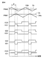
図22には、PWM制御部44a,44bの動作を説明するための波形図が示される。
図22を参照して、直流電源B1の制御指令信号VL1*は、キャリア波CW1とデューティ比DT1との電圧比較に基づくPWM制御によって生成される。DT1>CW1の期間では、制御指令信号VL1*がHレベルに設定される一方で、CW1<DT1の期間では、制御指令信号VL1*がLレベルに設定される。
FIG. 22 is a waveform diagram for explaining the operation of the
Referring to FIG. 22, control command signal VL1 * of DC power supply B1 is generated by PWM control based on voltage comparison between carrier wave CW1 and duty ratio DT1. In the period of DT1> CW1, the control command signal VL1 * is set to the H level, while in the period of CW1 <DT1, the control command signal VL1 * is set to the L level.
したがって、デューティ比DT1の上昇に応じて、制御指令信号VL1*のHレベル期間が長くなる。これにより、デューティ比DT1の上昇に応じて直流電源B1の出力が増加する一方で、デューティ比DT1の低下に応じて直流電源B1の出力が減少する。このように、直流電源B1からの出力制御のための制御指令信号VL1*に基づいて、下アーム素子(スイッチング素子Q2)のオン期間およびオフ期間の比率が制御される。 Therefore, as the duty ratio DT1 increases, the H level period of the control command signal VL1 * becomes longer. As a result, the output of the DC power supply B1 increases as the duty ratio DT1 increases, while the output of the DC power supply B1 decreases as the duty ratio DT1 decreases. In this way, the ratio between the on period and the off period of the lower arm element (switching element Q2) is controlled based on the control command signal VL1 * for output control from the DC power supply B1.
同様に、直流電源B2の制御指令信号VL2*は、キャリア波CW2とデューティ比DT2との電圧比較に基づくPWM制御によって生成される。DT2>CW2の期間では、制御指令信号VL2*がHレベルに設定される一方で、CW2<DT2の期間では、制御指令信号VL2*がLレベルに設定される。 Similarly, control command signal VL2 * of DC power supply B2 is generated by PWM control based on voltage comparison between carrier wave CW2 and duty ratio DT2. In the period of DT2> CW2, the control command signal VL2 * is set to the H level, while in the period of CW2 <DT2, the control command signal VL2 * is set to the L level.
したがって、デューティ比DT2の上昇に応じて、制御指令信号VL2*のHレベル期間が長くなる。これにより、デューティ比DT2の上昇に応じて直流電源B2の出力が増加する一方で、デューティ比DT2の低下に応じて直流電源B2の出力が減少する。このように、直流電源B2からの出力制御のための制御指令信号VL2*に基づいて、下アーム素子(スイッチング素子Q4)のオン期間およびオフ期間の比率が制御される。 Therefore, the H level period of control command signal VL2 * becomes longer as duty ratio DT2 increases. As a result, the output of the DC power supply B2 increases as the duty ratio DT2 increases, while the output of the DC power supply B2 decreases as the duty ratio DT2 decreases. Thus, the ratio of the on period and the off period of the lower arm element (switching element Q4) is controlled based on the control command signal VL2 * for output control from the DC power supply B2.
実施の形態1の変形例では、直流電源B1およびB2の出力制御に用いられるキャリア波の位相制御(以下、「キャリア位相制御」とも称する)が実行される。 In the modification of the first embodiment, carrier wave phase control (hereinafter also referred to as “carrier phase control”) used for output control of DC power supplies B1 and B2 is executed.
図23は、実施の形態1の変形例に従うキャリア位相制御の適用を説明するための波形図である。 FIG. 23 is a waveform diagram for explaining application of carrier phase control according to the modification of the first embodiment.
図23を参照して、キャリア位相制御の適用時には、キャリア波発生部45は、直流電源B1のPWM制御に用いられるキャリア波CW1と、直流電源B2のPWM制御に用いられるキャリア波CW2との間に位相差φを設ける。図23では、φ=180度の場合が例示される。
Referring to FIG. 23, when carrier phase control is applied, carrier
これに対して、図22に示された動作波形例では、キャリア波CW1およびCW2は、同一周波数かつ同一位相である。言い換えると、図22では、φ=0である。 On the other hand, in the operation waveform example shown in FIG. 22, the carrier waves CW1 and CW2 have the same frequency and the same phase. In other words, in FIG. 22, φ = 0.
位相差φが設けられた下でも、制御指令信号VL1*は、キャリア波CW1とデューティ比DT1との電圧比較に基づくPWM制御によって生成される。同様に、制御指令信号VL2*は、キャリア波CW2とデューティ比DT2との電圧比較に基づくPWM制御によって生成される。 Even under the phase difference φ, the control command signal VL1 * is generated by PWM control based on voltage comparison between the carrier wave CW1 and the duty ratio DT1. Similarly, control command signal VL2 * is generated by PWM control based on voltage comparison between carrier wave CW2 and duty ratio DT2.
図23において、デューティ比DT1,DT2は図22と同一値である。したがって、図23の制御指令信号VL1*は、図22の制御指令信号VL1*と比較して、位相は異なるもののHレベル期間の長さは同じである。同様に、図30の制御指令信号VL2*についても、図22の制御指令信号VL2*と比較して、位相は異なるもののHレベル期間の長さは同じである。 In FIG. 23, duty ratios DT1 and DT2 are the same values as in FIG. Therefore, the control command signal VL1 * of FIG. 23 has the same length of the H level period although the phase is different from that of the control command signal VL1 * of FIG. Similarly, the control command signal VL2 * in FIG. 30 has the same length of the H level period although the phase is different compared to the control command signal VL2 * in FIG.
キャリア波CW1およびCW2の間に位相差φを設けることにより、図23の制御指令信号VL1*,VL2*は、図22の制御指令信号VL1*,VL2*とは異なった波形となる。図22および図23の比較から、キャリア波CW1およびCW2の間の位相差φを変化させることにより、リアクトル電圧VL1,VL2間およびリアクトル電流IL1およびIL2間の位相関係についても変化することが理解される。 By providing phase difference φ between carrier waves CW1 and CW2, control command signals VL1 * and VL2 * in FIG. 23 have waveforms different from control command signals VL1 * and VL2 * in FIG. 22 and 23, it is understood that the phase relationship between reactor voltages VL1 and VL2 and between reactor currents IL1 and IL2 also changes by changing phase difference φ between carrier waves CW1 and CW2. The
一方で、同一のデューティ比DT1,DT2に対して、電流IL1およびIL2の平均値は、図22および図23の間で同等であることが理解される。すなわち、直流電源B1,B2の出力は、デューティ比DT1およびDT2によって制御されるものであり、キャリア波CW1,CW2間の位相差φを変化させても影響が生じない。 On the other hand, it is understood that the average values of currents IL1 and IL2 are equivalent between FIGS. 22 and 23 for the same duty ratios DT1 and DT2. In other words, the outputs of DC power supplies B1 and B2 are controlled by duty ratios DT1 and DT2, and there is no effect even if phase difference φ between carrier waves CW1 and CW2 is changed.
本実施の形態1の変形例では、キャリア波CW1,CW2間の位相差φを適切に調整するキャリア位相制御によって、可変磁気結合リアクトル100が磁気結合モードで動作するときの等価的なインダクタンスの増大効果を高める。
In the modification of the first embodiment, an equivalent inductance increase when the variable
図18および式(33),(34)を用いて説明したように、リアクトルL1,L2間に磁気結合が生じている状態において、リアクトル電流の変化率dIL1/dtおよびdIL2/dtの符号が異なる期間を長くするように、リアクトル電圧VL1,VL2の位相を制御すると、等価的にインダクタンスを高めることができる。具体的には、リアクトル電流IL1,IL2の傾きを小さくして、リップル電流を抑制することができる。 As described with reference to FIG. 18 and equations (33) and (34), in the state where magnetic coupling occurs between reactors L1 and L2, the signs of reactor current change rates dIL1 / dt and dIL2 / dt are different. When the phases of reactor voltages VL1 and VL2 are controlled so as to lengthen the period, inductance can be increased equivalently. Specifically, the ripple current can be suppressed by reducing the slopes of reactor currents IL1 and IL2.
したがって、制御指令信号VL1*,VL2*のHレベル期間の長さが、デューティ比DT1およびDT2によってそれぞれ規定される下で、制御指令信号VL1*,VL2*間の論理レベルが異なる期間がより長くなるようにパルス位相を調整すれば、上述した等価的なインダクタンスの増大効果をさらに高めることができる。 Therefore, the length of the H level period of the control command signals VL1 * and VL2 * is defined by the duty ratios DT1 and DT2, respectively, and the period in which the logic level between the control command signals VL1 * and VL2 * is different is longer. If the pulse phase is adjusted in such a way, the above-described equivalent inductance increasing effect can be further enhanced.
図24は、本実施の形態1の変形例に従うキャリア位相制御の動作例を説明するための波形図である。 FIG. 24 is a waveform diagram for explaining an operation example of carrier phase control according to the modification of the first embodiment.
図24を参照して、制御指令信号VL1*,VL2*のHレベル期間がそれぞれ同一の下でも、位相差φを調整することにより、制御指令信号VL1*,VL2*の論理レベルが異なる期間は変化する。図24に示されるように、位相差φ=φ*としたときに、制御指令信号VL1*がHレベルからLレベルへ遷移するタイミングと、制御指令信号VL2*がLレベルからHレベルへ遷移するタイミングとが同位相となる(時刻tx)。このとき、制御指令信号VL1*,VL2*の論理レベルが異なる期間を最も長く確保することができる。以下では、このような位相関係をもたらす位相差φ*を、最適位相差φ*とも称する。 Referring to FIG. 24, even when the H level periods of control command signals VL1 * and VL2 * are the same, a period in which the logical levels of control command signals VL1 * and VL2 * are different by adjusting phase difference φ Change. As shown in FIG. 24, when the phase difference φ = φ *, the timing at which the control command signal VL1 * changes from the H level to the L level, and the control command signal VL2 * changes from the L level to the H level. The timing is in phase (time tx). At this time, the longest period in which the logic levels of the control command signals VL1 * and VL2 * are different can be secured. Hereinafter, the phase difference φ * that causes such a phase relationship is also referred to as an optimum phase difference φ *.
ここで、図20に示された位相差φ=0のときの波形と、図24に示された位相差φ=φ*のときの波形とを比較する。制御指令信号VL2*の1周期に対する、図20での時刻t1〜t2およびt3〜t4期間の割合と、図24での時刻tz〜twの期間の割合との比較から、キャリア位相制御によって、デューティ比DT1,DT2が同一であるPWM制御の下で、リアクトル電流の変化率dIL1/dtおよびdIL2/dtの符号が異なる期間を長くできていることが理解される。 Here, the waveform when the phase difference φ = 0 shown in FIG. 20 is compared with the waveform when the phase difference φ = φ * shown in FIG. From the comparison of the ratio of the period from time t1 to t2 and t3 to t4 in FIG. 20 to the ratio of the period from time tz to tw in FIG. 24 with respect to one cycle of the control command signal VL2 *, the duty is determined by the carrier phase control. It is understood that the periods in which the signs of the reactor current change rates dIL1 / dt and dIL2 / dt are different can be extended under PWM control in which the ratios DT1 and DT2 are the same.
なお、図24の例とは逆に、制御指令信号VL1*がSD1がLレベルからHレベルへ遷移するタイミング(時刻ty)と、制御指令信号VL2*がHレベルからLレベルへ遷移するタイミング(時刻tz)が同位相となるように位相差φを設定した場合にも、制御指令信号VL1*,VL2*の論理レベルが異なる期間を同様に確保することができる。すなわち、このときの位相差φを最適位相差φ*とすることも可能である。 In contrast to the example of FIG. 24, the control command signal VL1 * has a timing (time ty) at which SD1 changes from L level to H level, and a timing at which the control command signal VL2 * changes from H level to L level ( Even when the phase difference φ is set so that the time tz) has the same phase, it is possible to similarly ensure a period in which the logic levels of the control command signals VL1 * and VL2 * are different. That is, the phase difference φ at this time can be set to the optimum phase difference φ *.
図24に示されるように、制御指令信号VL1*がHレベルからLレベルへ変化するタイミングで、リアクトル電流IL1も上昇から低下に転じる。すなわち、リアクトル電流IL1は極大となる。反対に、制御指令信号VL1*がLレベルからHレベルへ変化するタイミングで、リアクトル電流IL1も低下から上昇に転じる。すなわち、リアクトル電流IL1は極小となる。 As shown in FIG. 24, at the timing when control command signal VL1 * changes from the H level to the L level, reactor current IL1 also changes from increasing to decreasing. That is, reactor current IL1 becomes maximum. On the contrary, at the timing when the control command signal VL1 * changes from the L level to the H level, the reactor current IL1 also starts to decrease and increases. That is, reactor current IL1 is minimal.
このように、制御指令信号VL1*,VL2*の論理レベルが遷移するタイミングは、リアクトル電流IL1,IL2の変曲点(極大点または極小点)に対応する。したがって、上記のように、制御指令信号VL1*,VL2*の論理レベルが異なる期間を最も長く確保するために、制御指令信号VL1*,VL2*の論理レベルの遷移タイミングを一致させるように位相差φ=φ*に設定すると、リアクトル電流IL1およびIL2の変曲点が同一タイミングとなる。 As described above, the timing at which the logic levels of the control command signals VL1 * and VL2 * change corresponds to the inflection points (maximum points or minimum points) of the reactor currents IL1 and IL2. Therefore, as described above, in order to ensure the longest period in which the logical levels of the control command signals VL1 * and VL2 * are different from each other, the phase difference is set so that the transition timings of the logical levels of the control command signals VL1 * and VL2 * coincide. When φ = φ * is set, the inflection points of reactor currents IL1 and IL2 have the same timing.
図22〜図24からも理解されるように、制御指令信号VL1*,VL2*の波形は、デューティ比DT1,DT2によって決まる。したがって、図24のような制御指令信号VL1*,VL2*間の関係およびIL1,IL2の電流位相が実現できる最適位相差φ*についても、デューティ比DT1,DT2に応じて変わることが理解される。 As understood from FIGS. 22 to 24, the waveforms of the control command signals VL1 * and VL2 * are determined by the duty ratios DT1 and DT2. Therefore, it can be understood that the relationship between the control command signals VL1 * and VL2 * as shown in FIG. 24 and the optimum phase difference φ * at which the current phases of IL1 and IL2 can be realized also vary depending on the duty ratios DT1 and DT2. .
このため、デューティ比DT1,DT2と、最適位相差φ*との関係を予め求めるとともに、その対応関係を予めマップ(以下、「位相差マップ」とも称する)あるいは関数式(以下、「位相差算出式」とも称する)として制御装置40に記憶することが可能である。
For this reason, the relationship between the duty ratios DT1 and DT2 and the optimum phase difference φ * is obtained in advance, and the corresponding relationship is preliminarily mapped (hereinafter also referred to as “phase difference map”) or a function equation (hereinafter referred to as “phase difference calculation”). Can also be stored in the
可変磁気結合リアクトル100に含まれるリアクトルL1,L2の電流を制御する機能を有する制御装置40は、コントローラ43a,43b(図21)で算出されたデューティ比DT1,DT2に基づいて、上記位相差マップないし位相差算出式を参照して、最適位相差φ*を設定することができる。そして、キャリア波発生部45(図21)は、設定された最適位相差φ*を有するように、同一周波数のキャリア波CW1,CW2を発生する。
The
上記のような電流位相となるように、キャリア位相制御を適用して、可変磁気結合リアクトル100を通過するリアクトル電流IL1,IL2を制御することにより、リアクトルL1,L2間に磁気結合が生じている状態における等価的なインダクタンスの増大効果をさらに高めることができる。
By applying carrier phase control to control the reactor currents IL1 and IL2 passing through the variable
図25および図26には、本実施の形態に従う可変磁気結合リアクトルにおいてキャリア位相制御を適用したときの動作例が示される。図25および図26には、回路シミュレータによって解析された動作波形図が示される。 25 and 26 show an operation example when carrier phase control is applied to the variable magnetic coupling reactor according to the present embodiment. 25 and 26 show operation waveform diagrams analyzed by the circuit simulator.
図25を参照して、図25(a)には、リアクトルL1,L2間が磁気的に非結合であるときのシミュレーション波形が示され、図25(b)には、リアクトルL1,L2間が磁気的に結合状態であるときのシミュレーション波形が示される。図25(b)では、リアクトル電流IL1の極小点とリアクトル電流IL2の極大点とが同一タイミングとなるようにキャリア位相制御が適用されている。 Referring to FIG. 25, FIG. 25A shows a simulation waveform when the reactors L1 and L2 are not magnetically coupled, and FIG. 25B shows the relationship between reactors L1 and L2. Simulation waveforms when magnetically coupled are shown. In FIG. 25B, carrier phase control is applied so that the minimum point of the reactor current IL1 and the maximum point of the reactor current IL2 are at the same timing.
なお、図25(a),(b)の間では、回路定数を同一とした下で、リアクトル電流IL1の平均値同士およびIL2の平均値同士が同じになるようにシミュレーション条件が定められている。すなわち、図25(a)のシミュレーションでは、式(34)中のインダクタンスLa,Lb,Lc,Mabについては、図25(b)と同一値とした上で、Mxy=0としてシミュレーションを実行している。 25A and 25B, the simulation conditions are determined so that the average values of the reactor currents IL1 and the average values of IL2 are the same while the circuit constants are the same. . That is, in the simulation of FIG. 25 (a), the inductances La, Lb, Lc, and Mab in the equation (34) are set to the same values as in FIG. 25 (b), and the simulation is executed with Mxy = 0. Yes.
図25(b)のリアクトル電流IL1のピークトゥピーク値(リップル成分)は、図25(a)のリアクトル電流IL1のリップル成分よりも抑制されていることが、両者の比較から理解される。同様に、リアクトル電流IL2についても、図25(b)の方が、図25(a)よりもリップル成分が抑制されている。 It can be understood from a comparison between the two that the peak-to-peak value (ripple component) of the reactor current IL1 in FIG. 25B is suppressed more than the ripple component of the reactor current IL1 in FIG. Similarly, with respect to the reactor current IL2, the ripple component in FIG. 25 (b) is suppressed more than in FIG. 25 (a).
図25(b)では、特に、小電流側のリアクトル電流IL2のピーク抑性に効果があることが理解される。すなわち、リアクトル電流IL2の極大点とリアクトル電流IL1の極小点とが同一タイミングとなるようにキャリア位相制御を行なうとリアクトル電流IL2のピーク抑制に効果がある。
Figure 25 (b), the particular, it is understood that the effect on the peak suppression sexual reactor
図26を参照して、図26(a)には、図25(a)と同一の波形、すなわち、リアクトルL1,L2間が磁気的に非結合であるときのシミュレーション波形が示される。図26(b)には、リアクトルL1,L2間が磁気的に結合状態であるときのシミュレーション波形が示される。図26(b)では、リアクトル電流IL1の極大点とリアクトル電流IL2の極小点とが同一タイミングとなるように、すなわち、図26と同等の電流位相となるように、キャリア位相制御が適用される。なお、図26(a),(b)の間でも、シミュレーション条件は、図25(a),(b)と同様である。 Referring to FIG. 26, FIG. 26 (a) shows the same waveform as FIG. 25 (a), that is, a simulation waveform when the reactors L1 and L2 are not magnetically coupled. FIG. 26B shows a simulation waveform when the reactors L1 and L2 are magnetically coupled. In FIG. 26B, the carrier phase control is applied so that the maximum point of the reactor current IL1 and the minimum point of the reactor current IL2 have the same timing, that is, the current phase is equivalent to that in FIG. . Note that the simulation conditions are the same as those in FIGS. 25A and 25B even between FIGS. 26A and 26B.
図26(b)のリアクトル電流IL1のピークトゥピーク値(リップル成分)は、図26(a)のリアクトル電流IL1のリップル成分よりも抑制されていることが、両者の比較から理解される。同様に、リアクトル電流IL2についても、図26(b)の方が、図26(a)よりもリップル成分が抑制されている。 It can be understood from a comparison between the two that the peak-to-peak value (ripple component) of the reactor current IL1 in FIG. 26B is suppressed more than the ripple component of the reactor current IL1 in FIG. Similarly, with respect to the reactor current IL2, the ripple component in FIG. 26 (b) is suppressed more than in FIG. 26 (a).
図26(b)では、特に、大電流側のリアクトル電流IL1のピーク抑性に効果があることが理解される。すなわち、リアクトル電流IL1の極大点とリアクトル電流IL2の極小点とが同一タイミングとなるようにキャリア位相制御を行なうとリアクトル電流IL1のピーク抑制に効果がある。 In FIG. 26B, it is understood that the peak current suppression of the reactor current IL1 on the large current side is particularly effective. That is, if carrier phase control is performed so that the maximum point of reactor current IL1 and the minimum point of reactor current IL2 are at the same timing, it is effective in suppressing the peak of reactor current IL1.
これらのシミュレーション波形から、本実施の形態に従う可変磁気結合リアクトルでは、リアクトルL1,L2間が磁気的に結合するように動作させることで、リアクトル電流IL1,IL2のリップル成分を抑性、すなわち、等価的にインダクタンスを増大できることが理解される。 From these simulation waveforms, in the variable magnetic coupling reactor according to the present embodiment, the ripple components of reactor currents IL1 and IL2 are suppressed, that is, equivalent, by operating so that reactors L1 and L2 are magnetically coupled. It can be understood that the inductance can be increased.
さらに、図25(b)および図26(b)では、キャリア位相制御の適用により、リアクトル電流IL1の傾き(変化率)の符号と、リアクトル電流IL2の傾き(変化率)の符号とが異なる期間Taを長くし、両符号が同じである期間Tbを短くすることができる。この結果、可変磁気結合リアクトルにおけるインダクタンス増大効果を高めることができる。これらの等価的なインダクタンス増大効果により、共通化されたコア150を用いて2個のリアクトルL1,L2を一体化した複合磁気部品によって可変磁気結合リアクトルを構成することによって、リアクトルの小型軽量化を図ることができる。
Further, in FIG. 25B and FIG. 26B, periods in which the sign of the slope (change rate) of reactor current IL1 and the sign of the slope (change rate) of reactor current IL2 are different due to the application of carrier phase control. longer ta, can be both code to shorten the period T b is the same. As a result, the effect of increasing the inductance in the variable magnetic coupling reactor can be enhanced. Due to these equivalent inductance increasing effects, a variable magnetic coupling reactor is formed by a composite magnetic component in which two reactors L1 and L2 are integrated using a
[他の電流領域での動作]
以上、実施の形態1およびその変形例では、リアクトル電流IL1およびIL2が共に正の領域(IL1>0,IL2>0)における可変磁気結合リアクトルの動作を説明した。この状態では、直流電源B1,B2の両方が電力を供給(放電)している。
[Operation in other current regions]
As described above, in the first embodiment and the modifications thereof, the operation of the variable magnetic coupling reactor in the region where reactor currents IL1 and IL2 are both positive (IL1> 0, IL2> 0) has been described. In this state, both DC power supplies B1 and B2 supply (discharge) power.
しかしながら、実施の形態1およびその変形例で説明した可変磁気結合リアクトルが適用された電源システム5は、直流電源B1,B2の少なくとも一方が充電されるような、上記以外の電流領域でも動作することができる。すなわち、上記可変磁気結合リアクトルは、IL1<0,IL2<0の領域、IL1>0,IL2<0の領域、IL1<0,IL2>0の電流領域でも同様に動作することができる。
However, the
図27は、リアクトル電流およびリアクトル電圧の極性の各組み合わせにおける可変磁気結合リアクトルの動作を説明するための図表である。 FIG. 27 is a chart for explaining the operation of the variable magnetic coupling reactor in each combination of the polarities of the reactor current and the reactor voltage.
図27を参照して、リアクトル電流IL1,IL2にそれぞれ相当する電流ix,iyと、リアクトルL1,L2への印加電圧である電圧Vx,Vyとの極性(正/負)の組み合わせによって、リアクトルL1,L2は、パターン1〜24の24個の動作パターンを有する。図27中では、リアクトル電流IL1,IL2による磁界が強め合う磁脚部を「+」と表記する一方で、磁界が弱め合う磁脚部を「−」と表記する。 Referring to FIG. 27, reactor L1 is based on a combination of polarities (positive / negative) of currents ix, iy respectively corresponding to reactor currents IL1, IL2 and voltages Vx, Vy applied to reactors L1, L2. , L2 have 24 operation patterns of patterns 1-24. In FIG. 27, a magnetic leg portion in which the magnetic fields by the reactor currents IL1 and IL2 strengthen each other is represented as “+”, while a magnetic leg portion in which the magnetic fields weaken each other is represented as “−”.
パターン1〜4は、上述した、IL1>0かつIL2>0のときの動作パターンである。これらの動作パターンでは、上述のように、磁脚部152で磁界が強め合う一方で、磁脚部151では磁界が弱め合う。この場合には、式(33)中の(R2−R1)が、非磁気結合モードでR2−R1=0となる一方で、磁気結合モードでは(R2−R1)>0となる。すなわち、(R2−R1)≧0である。このため、式(33)の逆行列を求めることによって得られる式(34)において、Mxy≦0となる。
この場合には、式(33)において、(R1+R2)>0、かつ、(R1+R2+4R3)>0であることから、VxおよびVyの符号が異なるときの方が、VxおよびVyの符号が同じときと比較して、|dix/dt|,|diy/dt|は小さくなる。したがって、VxとVyの符号が異なるパターン2および3において、|dix/dt|,|diy/dt|が減少する。一方で、VxとVyの符号が同じであるパターン1および4では、|dix/dt|,|diy/dt|は増大する。
In this case, since (R1 + R2)> 0 and (R1 + R2 + 4R3)> 0 in the formula (33), when the signs of Vx and Vy are different, the signs of Vx and Vy are the same. In comparison, | dix / dt |, | diy / dt | Therefore, in
パターン13〜16は、IL1<0かつIL2<0のときの動作パターンである。これらのパターン13〜16では、リアクトル電流IL1による磁界の方向と、リアクトル電流IL2による磁界の方向との相対的な関係は、IL1>0,IL2>0のときと同様である。したがって、これらの動作パターンにおいても、磁脚部152で磁界が強め合う一方で、磁脚部151では磁界が弱め合う。
したがって、パターン13〜16においても、(R2−R1)≧0である。すなわち、VxおよびVyの符号が異なるパターン14および15において、|dix/dt|,|diy/dt|が減少する。一方で、VxおよびVyの符号が同じであるパターン13および16では、|dix/dt|,|diy/dt|は増大する。
Therefore, also in the
このように、リアクトル電流IL1,IL2の極性(正/負)が同じ場合には、VxおよびVyの符号が異なることが、リアクトル電流IL1,IL2のリップル電流振幅が小さくなる、すなわち、リアクトルL1,L2のインダクタンスが等価的に増加する条件となる。 As described above, when the polarities (positive / negative) of reactor currents IL1 and IL2 are the same, the fact that the signs of Vx and Vy are different reduces the ripple current amplitude of reactor currents IL1 and IL2, that is, reactors L1 and L1. This is a condition that the inductance of L2 increases equivalently.
したがって、実施の形態1の変形例で説明したキャリア位相制御を適用する場合には、図25および図26で説明したように、一方のリアクトル電流の極大点と他方のリアクトル電流の極小点とが同一タイミングとなるように位相差φを制御することによって、リアクトル電流IL1,IL2のリップル電流振幅を抑性できる。 Therefore, when the carrier phase control described in the modification of the first embodiment is applied, as described in FIGS. 25 and 26, the maximum point of one reactor current and the minimum point of the other reactor current are The ripple current amplitude of reactor currents IL1 and IL2 can be suppressed by controlling phase difference φ so as to have the same timing.
これに対して、パターン5〜8は、IL1>0かつIL2<0のときの動作パターンであり、パターン9〜12は、IL1<0かつIL2>0のときの動作パターンである。すなわち、パターン5〜12では、リアクトル電流IL1およびIL2の極性(正/負)が異なる。
On the other hand,
したがって、パターン5〜12では、リアクトル電流IL1による磁界の方向と、リアクトル電流IL2による磁界の方向との相対的な関係は、図10,11等で説明したのと反対である。したがって、これらの動作パターンでは、実施の形態1で説明したのとは反対に、磁脚部151で磁界が強め合う一方で、磁脚部152では磁界が弱め合う。この場合には、式(33)中の(R2−R1)が、非磁気結合モードでR2−R1=0となる一方で、磁気結合モードでは(R2−R1)<0となる。すなわち、(R2−R1)≦0である。このため、式(34)において、Mxy≧0となる。
Therefore, in the
この場合には、式(33)において(R1+R2)>0、かつ、(R1+R2+4R3)>0であることを考慮すると、VxおよびVyの符号が同じであるときの方が、VxおよびVyの符号が異なるときと比較して、|dix/dt|,|diy/dt|は小さくなる。したがって、VxおよびVyの符号が同じである、パターン5、8、9および12において、|dix/dt|,|diy/dt|が減少する。一方で、VxおよびVyの符号が異なる、6、7、10および11では、|dix/dt|,|diy/dt|は増大する。
In this case, considering that (R1 + R2)> 0 and (R1 + R2 + 4R3)> 0 in the equation (33), the sign of Vx and Vy is greater when the signs of Vx and Vy are the same. Compared to a different time, | dix / dt |, | diy / dt | Therefore, in
したがって、リアクトル電流IL1,IL2の極性(正/負)が異なる場合には、VxおよびVyの符号が同じであることが、リアクトル電流IL1,IL2のリップル電流振幅が小さくなる、すなわち、リアクトルL1,L2のインダクタンスが等価的に増加する条件となる。 Therefore, when the polarities (positive / negative) of reactor currents IL1 and IL2 are different, the same sign of Vx and Vy reduces the ripple current amplitude of reactor currents IL1 and IL2, that is, reactor L1, This is a condition that the inductance of L2 increases equivalently.
なお、パターン5〜12において、実施の形態1の変形例で説明したキャリア位相制御を適用する場合には、リアクトル電流IL1,IL2のリップル成分を抑性するための条件が、図25および図26での説明とは異なる。具体的には、一方のリアクトル電流の極大点と他方のリアクトル電流の極大点とが同一タイミングとなるように、あるいは、一方のリアクトル電流の極小点と他方のリアクトル電流の極小点とが同一タイミングとなるように位相差φを制御すれば、リアクトル電流IL1,IL2のリップル成分を抑性することができる。
In the
このように、本実施の形態1に従う可変磁気結合リアクトルは、リアクトル電流IL1,IL2の電流方向が変化しても、上述したように、リアクトルL1およびL2は、非磁気結合モードおよび磁気結合モードの両方で動作することができる。そして、リアクトルL1,L2への印加電圧Vx,Vyの極性の組み合わせに応じて、電流リップル成分を減少ないし増大させることができる。 Thus, in the variable magnetic coupling reactor according to the first embodiment, as described above, reactors L1 and L2 are in the nonmagnetic coupling mode and the magnetic coupling mode even if the current direction of reactor currents IL1 and IL2 changes. Can work with both. The current ripple component can be reduced or increased in accordance with the combination of the polarities of the voltages Vx and Vy applied to the reactors L1 and L2.
さらに、実施の形態1の変形例に従うキャリア位相制御を適用することによって、リアクトル電流IL1,IL2の変曲点を同一タイミングとすれば、電流リップルの増大ないし低減を制御することも可能である。特に、電流リップルを減少するための最適位相差は、リアクトル電流IL1,IL2の極性(正/負)が同じである場合と、異なる場合とで異なる。 Further, by applying carrier phase control according to the modification of the first embodiment, if the inflection points of reactor currents IL1 and IL2 are set at the same timing, it is also possible to control the increase or reduction of current ripple. In particular, the optimum phase difference for reducing the current ripple differs depending on whether the polarities (positive / negative) of reactor currents IL1 and IL2 are the same or different.
[実施の形態2]
実施の形態2では、可変磁気結合リアクトルの構造の変形例を説明する。すなわち、実施の形態2に従う可変磁気結合リアクトルは、実施の形態1に従う可変磁気結合リアクトルと同様に動作することができる。
[Embodiment 2]
In the second embodiment, a modified example of the structure of the variable magnetic coupling reactor will be described. That is, the variable magnetic coupling reactor according to the second embodiment can operate in the same manner as the variable magnetic coupling reactor according to the first embodiment.
図28には、実施の形態2に従う可変磁気結合リアクトル100♯の概略的な外観が斜視図によって示される。
FIG. 28 is a perspective view showing a schematic appearance of variable
図28を参照して、実施の形態2に従う可変磁気結合リアクトル100♯は、コア150♯と、巻線121a♯,121b♯,122♯とを含む。巻線121a♯および121b♯は、巻線121aおよび121bと同様に、電気的に直列接続されて、リアクトルL1のコイルを構成する。巻線122♯は、リアクトルL2のコイルを構成する。可変磁気結合リアクトル100♯においても、リアクトルL1を構成する巻線121a♯,121b♯と、リアクトルL2を構成する巻線122♯とは、共通のコア150♯の別個の部位にそれぞれ巻回されている。
Referring to FIG. 28, variable
図29は、図28に示された可変磁気結合リアクトルのコア150♯の外観を示す平面図である。
FIG. 29 is a plan view showing an appearance of
図29を参照して、コア150♯は、円環形状の外形部位と、外形部位から円環の中心に向かって延在する磁脚部151♯〜153♯とを有する。磁脚部151♯〜153♯は、円環の中心部で一体化される。すなわち、コア150♯では、外形部位および中心部位によって、可変磁気結合リアクトル100の磁脚部154と同様の磁脚部154♯が形成される。磁脚部151♯〜153♯には、ギャップ161♯〜163♯が設けられる。
Referring to FIG. 29,
磁脚部151♯〜153♯は、コア150♯における巻線121a♯,121b♯,122♯の巻回部位に相当する。一方で、磁脚部154♯は、コア150♯における巻線の非巻回部位に相当し、巻線が巻回された磁脚部151♯〜153♯の間に磁気経路を形成するように機能する。
図30は、実施の形態2に従う可変磁気結合リアクトルにおける各巻線の巻回態様を説明するための概略的な平面図である。 FIG. 30 is a schematic plan view for illustrating a winding mode of each winding in the variable magnetic coupling reactor according to the second embodiment.
図30を参照して、端子201♯および202♯の間にリアクトル電流IL1が流される。導線121c♯によって、巻線121a♯および121b♯の間は、電気的に直列接続される。図30には、実施の形態1と同様に、IL1>0,IL2>0のときの電流方向が示される。
Referring to FIG. 30, reactor current IL1 flows between
リアクトル電流IL1が巻線121a♯および巻線121b♯を流れることによって、巻線121a♯から磁界211♯が生じるとともに、巻線121b♯から磁界212♯が生じる。この結果、磁界211♯は、円環中心側をN極とし、円環外周側をS極とする方向を有する。一方で、磁界212♯は、円環外周側をN極とし、円環中心側をS極とする方向を有する。すなわち、リアクトル電流IL1の通流によって、巻線121a♯,121b♯からそれぞれ発生される磁界211♯,212♯は、互いに反対方向であり、図6に示された磁界211および212と同様に、コア150♯内で、磁脚部151♯および152♯を含む一巡経路を形成する。このような磁界方向が実現されるように、導線121c♯は、巻線121a♯および121b♯の間に接続される。
Reactor current IL1 flows through winding 121a # and winding 121b #, thereby generating
さらに、端子203♯および204♯の間に、リアクトル電流IL2が流される(図30では、IL1>0,IL2>0)。これにより、巻線122♯からは磁界213♯が発生される。磁界213♯は、円環中心側をN極とし、円環外周側をS極とする方向を有する。すなわち、同一方向のリアクトル電流IL1,IL2によって、巻線122♯が生じる磁界213♯は、巻線121a♯からの磁界211♯とは同じ方向である一方で、巻線121b♯からの磁界212♯とは逆の方向である。
Furthermore, reactor current IL2 flows between
図31は、リアクトルL1の電流通流時における発生磁束の関係を説明するための概念図である。 FIG. 31 is a conceptual diagram for explaining the relationship of magnetic flux generated when current flows through reactor L1.
図31を参照して、磁脚部151♯に巻回された巻線121a♯から発生される磁界211♯(図30)による磁束221♯は、磁脚部154♯を含む磁気経路を経由して、磁脚部152♯および153♯にも作用する。同様に、磁脚部152♯に巻回された巻線121b♯から発生される磁界212♯(図30)による磁束222♯は、磁脚部154♯を含む磁気経路を経由して、磁脚部151♯および153♯にも作用する。
Referring to FIG. 31,
磁脚部151♯および152♯の各々において、磁界211♯および212♯による磁束221♯および222♯は同一方向に作用する。すなわち、磁界211♯および212♯は、磁脚部151♯および152♯の各々において、互いに強め合う。
In each of
一方、磁脚部153♯において、磁界211♯および212♯による磁束221♯および222♯は反対方向に作用する。すなわち、磁界211♯および212♯は、磁脚部153♯において、互いに弱め合う。
On the other hand, in
図32は、リアクトルL2の電流通流時における発生磁束の関係を説明するための概念図である。 FIG. 32 is a conceptual diagram for explaining the relationship of magnetic flux generated when current flows through reactor L2.
図32を参照して、磁脚部153♯に巻回された巻線122♯から発生される磁界213♯(図30)による磁束223♯は、磁脚部154♯を経由して、磁脚部151♯および152♯にも作用する。
Referring to FIG. 32,
図33には、リアクトルL1,L2の両方への電流通流時における発生磁束の関係を説明するための概念図が示される。 FIG. 33 is a conceptual diagram for explaining the relationship between magnetic fluxes generated when current flows to both reactors L1 and L2.
図33を参照して、リアクトルL2に対応する磁脚部153♯では、図31に示したように、巻線121a♯からの磁束221♯と巻線121b♯からの磁束222♯とが打ち消し合うため、巻線122♯による磁束223♯が通過する。すなわち、磁脚部153♯での磁界の大きさは、リアクトル電流IL2によって生じる磁界213♯相当である。
Referring to FIG. 33, in
これに対して、リアクトルL1に対応する磁脚部151♯および152♯の間では、リアクトルL2からの磁束との干渉によって、磁界の大きさが不均衡になる。具体的には、磁脚部152♯では、磁界211♯,212♯(図30)による磁束221♯,222♯と、磁界213♯(図30)による磁束223♯とは同じ方向である。このため、磁脚部152♯では、磁界211♯,212♯と磁界213♯とは強め合う。
On the other hand, between the
これに対して、磁脚部151♯では、磁界211♯,212♯(図30)による磁束221♯,222♯と、磁界213♯(図30)による磁束223♯とは反対方向であるので、磁界211♯および212♯と磁界213♯とは弱め合う。
On the other hand, in
このように、可変磁気結合リアクトル100♯における、リアクトル電流IL1,IL2の通流による磁脚部151♯〜153♯での磁気的な挙動は、実施の形態1に従う可変磁気結合リアクトル100の磁脚部151〜153と同様である。すなわち、実施の形態2に従う可変磁気結合リアクトル100♯において、磁脚部151♯は「第1の磁脚部」に対応し、磁脚部152♯は「第2の磁脚部」に対応する。また、磁脚部153♯は「第3の磁脚部」に対応する。
Thus, the magnetic behavior in
このように、実施の形態2に従う可変磁気結合リアクトル100♯は、実施の形態1に従う可変磁気結合リアクトル100と同様に、リアクトル電流IL1,IL2に応じて、リアクトルL1およびL2が非磁気結合モードおよび磁気結合モードの両方で動作することができる。リアクトル電流IL1,IL2およびリアクトル印加電圧Vx,Vyの極性(正/負)の組み合わせに応じたリアクトルL1,L2の動作、特に、電流リップル成分を減少ないし増大させる条件についても、実施の形態1と同様であるので詳細な説明は繰り返さない。また、実施の形態2に従う可変磁気結合リアクトル100♯に対しても、実施の形態1の変形例に従うキャリア位相制御の適用することが可能である。この場合における、電流リップルを増大ないし低減する条件についても、実施の形態1で説明したのと同様であるので詳細な説明は繰り返さない。
Thus, similarly to variable
[実施の形態3]
実施の形態3では、実施の形態1で説明した可変磁気結合リアクトル100が適用される電源システムの他の構成例について説明する。
[Embodiment 3]
In the third embodiment, another configuration example of the power supply system to which the variable
図34は、本発明の実施の形態3に従う電源システム5cの構成を示す回路図である。
図34を参照して、実施の形態3に従う電源システムで5cは、直流電源B1,B2と、電力変換器50と、制御装置40とを備える。図1に示した電源システム5と比較して、実施の形態3に従う電源システム5cは、電力変換器6および7に代えて、電力変換器50が設けられた構成を有する。電力変換器50は、直流電源B1,B2と、負荷30との間に接続される。電力変換器50は、負荷30と接続された電力線PL上の直流電圧(出力電圧VH)を電圧指令値VH*に従って制御する。
FIG. 34 is a circuit diagram showing a configuration of
Referring to FIG. 34, the
電力変換器50は、スイッチング素子S1〜S4と、リアクトルL1,L2とを含む。スイッチング素子S1〜S4に対しては、逆並列ダイオードD1〜D4が配置されている。スイッチング素子S1〜S4は、制御装置40からの制御信号SG1〜SG4に応答して、オンオフを制御される。
スイッチング素子S1は、高電圧側の電力線PLおよびノードN1の間に電気的に接続される。スイッチング素子S2はノードN1およびN2の間に電気的に接続される。スイッチング素子S3は、ノードN2およびN3の間に電気的に接続される。スイッチング素子S4は、ノードN3および低電力側の電力線GLの間に電気的に接続される。電力線GLは、負荷30および、直流電源B1の負極端子に対して電気的に接続される。 Switching element S1 is electrically connected between power line PL on the high voltage side and node N1. Switching element S2 is electrically connected between nodes N1 and N2. Switching element S3 is electrically connected between nodes N2 and N3. Switching element S4 is electrically connected between node N3 and low-power side power line GL. Power line GL is electrically connected to load 30 and the negative terminal of DC power supply B1.
リアクトルL1は、ノードN2および電力線GLの間に電気的に、直流電源B1と直列に接続される。リアクトルL2は、ノードN1およびノードN3の間に電気的に、直流電源B2と直列に接続される。図34の構成例では、リアクトルL2の端子203は、直流電源B2の正極端子と電気的に接続される。リアクトルL2の端子204は、ノードN1と電気的に接続される。これにより、リアクトルL2は、ノードN1およびノードN3の間に、直流電源B2と直列に電気的に接続される。
Reactor L1 is electrically connected in series with DC power supply B1 between node N2 and power line GL. Reactor L2 is electrically connected in series with DC power supply B2 between nodes N1 and N3. In the configuration example of FIG. 34,
電力変換器50を含む電源システム5cにおいて、リアクトルL1およびL2は、一体化されたコアによる複合磁気部品である、実施の形態1,2に従う可変磁気結合リアクトル100,100♯によって構成される。
In
また図34の例では、リアクトルL1の端子201は、直流電源B1の正極端子と電気的に接続される。リアクトルL1の端子202は、ノードN2と電気的に接続される。これにより、リアクトルL1は、ノードN2と電力線GLとの間に、直流電源B1と直列に電気的に接続される。
In the example of FIG. 34, the
図34から理解されるように、電力変換器50は、直流電源B1および直流電源B2の各々に対応して昇圧チョッパ回路を備えた構成となっている。すなわち、直流電源B1に対しては、スイッチング素子S1,S2を上アーム素子とする一方で、スイッチング素子S3,S4を下アーム素子とする電流双方向の第1の昇圧チョッパ回路が構成される。
As understood from FIG. 34,
同様に、直流電源B2に対しては、スイッチング素子S1,S4を上アーム素子とする一方で、スイッチング素子S2,S3を下アーム素子とする電流双方向の第2の昇圧チョッパ回路が構成される。そして、第1の昇圧チョッパ回路によって直流電源B1および電力線PL,GLの間に形成される第1の電力変換経路と、第2の昇圧チョッパ回路によって直流電源B2および電力線PL,GLの間に形成される第2の電力変換経路との両方に、スイッチング素子S1〜S4が含まれる。さらに、リアクトルL1およびL2は、上記第1および第2の電力変換経路にそれぞれ含まれる。 Similarly, for DC power supply B2, a current bidirectional second step-up chopper circuit is configured with switching elements S1 and S4 as upper arm elements and switching elements S2 and S3 as lower arm elements. . Then, a first power conversion path formed between the DC power supply B1 and the power lines PL and GL by the first boost chopper circuit, and a DC power supply B2 and the power lines PL and GL formed by the second boost chopper circuit. The switching elements S1 to S4 are included in both of the second power conversion path. Furthermore, reactors L1 and L2 are included in the first and second power conversion paths, respectively.
以下に詳細に説明するように、電力変換器50は、負荷30に対して直流電源B1およびB2を並列に接続してDC/DC変換を実行するモード(以下、「パラレル昇圧モード」とも称する)と、負荷30に対して直流電源B1およびB2を直列に接続してDC/DC変換を実行するモード(以下、「シリーズ昇圧モード」とも称する)とを切換可能に構成されている。特に、電力変換器50は、スイッチング素子S1〜S4の制御によって、パラレル昇圧モードおよびシリーズ昇圧モードを切替えて動作することが可能である。
As will be described in detail below,
(パラレル昇圧モードでの回路動作)
電力変換器50のパラレル昇圧モードでの回路動作について説明する。
(Circuit operation in parallel boost mode)
The circuit operation of the
図35には、パラレル昇圧モードにおける直流電源B1に対するDC/DC変換(昇圧動作)が示される。 FIG. 35 shows DC / DC conversion (boost operation) for DC power supply B1 in the parallel boost mode.
図35(a)を参照して、スイッチング素子S3,S4のペアをオンし、スイッチング素子S1,S2のペアをオフすることによって、リアクトルL1にエネルギを蓄積するための電流経路350が形成される。これにより、昇圧チョッパ回路の下アーム素子をオンした状態が形成される。
Referring to FIG. 35A, by turning on the pair of switching elements S3 and S4 and turning off the pair of switching elements S1 and S2, a
これに対して、図35(b)を参照して、スイッチング素子S3,S4のペアをオフするとともに、スイッチング素子S1,S2のペアをオンすることによって、リアクトルL1の蓄積エネルギを直流電源B1のエネルギとともに出力するための電流経路351が形成される。これにより、昇圧チョッパ回路の上アーム素子をオンした状態が形成される。
On the other hand, referring to FIG. 35 (b), the pair of switching elements S3 and S4 is turned off, and the pair of switching elements S1 and S2 is turned on, whereby the stored energy of reactor L1 is supplied to DC power supply B1. A
スイッチング素子S3,S4のペアがオンされる一方で、スイッチング素子S1,S2の少なくとも一方がオフされている第1の期間と、スイッチング素子S1,S2のペアがオンされる一方で、スイッチング素子S3,S4の少なくとも一方がオフされている第2の期間とを交互に繰返すことにより、図35(a)の電流経路350および図35(b)の電流経路351が交互に形成される。
While the pair of switching elements S3 and S4 is turned on, the first period in which at least one of the switching elements S1 and S2 is turned off and the pair of switching elements S1 and S2 are turned on, while the switching element S3 , S4 and the second period in which at least one of them is turned off alternately, the
この結果、スイッチング素子S1,S2のペアを等価的に上アーム素子とし、スイッチング素子S3,S4のペアを等価的に下アーム素子とする昇圧チョッパ回路が、直流電源B1に対して構成される。図35に示されるDC/DC変換動作では、直流電源B2への電流流通経路がないため、直流電源B1およびB2は互いに非干渉である。すなわち、直流電源B1およびB2に対する電力の入出力を独立に制御することが可能である。 As a result, a step-up chopper circuit having a pair of switching elements S1 and S2 equivalently as an upper arm element and a pair of switching elements S3 and S4 equivalently as a lower arm element is configured for DC power supply B1. In the DC / DC conversion operation shown in FIG. 35, since there is no current flow path to DC power supply B2, DC power supplies B1 and B2 are non-interfering with each other. That is, it is possible to independently control power input / output to / from DC power supplies B1 and B2.
このようなDC/DC変換において、直流電源B1の電圧V[1]と、電力線PLの出力電圧VHとの間には、式(1)と同様に、下記(35)式に示す関係が成立する。式(35)では、スイッチング素子S3,S4のペアがオンされる第1の期間のデューティ比をDaとする。 In such DC / DC conversion, the relationship shown in the following equation (35) is established between the voltage V [1] of the DC power supply B1 and the output voltage VH of the power line PL, as in the equation (1). To do. In equation (35), let Da be the duty ratio in the first period during which the pair of switching elements S3 and S4 is turned on.
VH=1/(1−Da)・V[1] …(35)
図36には、パラレル昇圧モードにおける直流電源B2に対するDC/DC変換(昇圧動作)が示される。
VH = 1 / (1-Da) · V [1] (35)
FIG. 36 shows DC / DC conversion (boost operation) for DC power supply B2 in the parallel boost mode.
図36(a)を参照して、スイッチング素子S2,S3のペアをオンし、スイッチング素子S1,S4のペアをオフすることによって、リアクトルL2にエネルギを蓄積するための電流経路360が形成される。これにより、昇圧チョッパ回路の下アーム素子をオンした状態が形成される。
Referring to FIG. 36A, by turning on the pair of switching elements S2 and S3 and turning off the pair of switching elements S1 and S4, a
これに対して、図36(b)を参照して、スイッチング素子S2,S3のペアをオフするとともに、スイッチング素子S1,S4のペアをオンすることによって、リアクトルL2の蓄積エネルギを直流電源B2のエネルギとともに出力するための電流経路361が形成される。これにより、昇圧チョッパ回路の上アーム素子をオンした状態が形成される。
On the other hand, referring to FIG. 36 (b), the pair of switching elements S2 and S3 is turned off, and the pair of switching elements S1 and S4 is turned on, whereby the stored energy of reactor L2 is supplied to DC power supply B2. A
スイッチング素子S2,S3のペアがオンされる一方で、スイッチング素子S1,S4の少なくとも一方がオフされている第1の期間と、スイッチング素子S1,S4のペアがオンされる一方で、スイッチング素子S2,S3の少なくとも一方がオフされている第2の期間とを交互に繰返すことにより、図36(a)の電流経路360および図36(b)の電流経路361が交互に形成される。
While the pair of switching elements S2 and S3 is turned on, the first period when at least one of the switching elements S1 and S4 is turned off, and the pair of switching elements S1 and S4 is turned on, while the switching element S2 , S3 are alternately turned off and the second period in which the
この結果、スイッチング素子S1,S4のペアを等価的に上アーム素子とし、スイッチング素子S2,S3のペアを等価的に下アーム素子とする昇圧チョッパ回路が、直流電源B2に対して構成される。図36に示されるDC/DC変換動作では、直流電源B1を含む電流経路がないため、直流電源B1およびB2は互いに非干渉である。 As a result, a step-up chopper circuit having a pair of switching elements S1 and S4 equivalently as an upper arm element and a pair of switching elements S2 and S3 equivalently as a lower arm element is configured for DC power supply B2. In the DC / DC conversion operation shown in FIG. 36, since there is no current path including DC power supply B1, DC power supplies B1 and B2 are non-interfering with each other.
このようなDC/DC変換において、直流電源B2の電圧V[2]と、電力線PLの出力電圧VHとの間には、下記(36)式に示す関係が成立する。(36)式では、スイッチング素子S2,S3のペアがオンされる第1の期間のデューティ比をDbとする。 In such DC / DC conversion, the relationship expressed by the following equation (36) is established between the voltage V [2] of the DC power supply B2 and the output voltage VH of the power line PL. In the equation (36), Db is a duty ratio in the first period in which the pair of switching elements S2 and S3 is turned on.
VH=1/(1−Db)・V[2] …(36)
上述のように、電力変換器50のパラレル昇圧モードでは、実施の形態1と同様に、リアクトルL1を流れる電流と、リアクトルL2を流れる電流とは独立に制御される。この結果、直流電源B1およびB2に対する電力の入出力を独立に制御することが可能である。
VH = 1 / (1-Db) · V [2] (36)
As described above, in the parallel boost mode of
直流電源B1の出力を制御するためのデューティ比Daと、直流電源B2の出力を制御するためのデューティ比Dbとは、たとえば、図2または図21と同等の制御構成によって求めることができる。すなわち、デューティ比Daは、実施の形態1およびその変形例におけるデューティ比DT1と同様に算出できる。また、デューティ比Dbは、実施の形態1およびその変形例におけるデューティ比DT2と同様に算出できる。 The duty ratio Da for controlling the output of the DC power supply B1 and the duty ratio Db for controlling the output of the DC power supply B2 can be obtained, for example, by a control configuration equivalent to that shown in FIG. That is, the duty ratio Da can be calculated in the same manner as the duty ratio DT1 in the first embodiment and its modification. Further, the duty ratio Db can be calculated in the same manner as the duty ratio DT2 in the first embodiment and its modification.
図37には、パラレル昇圧モードにおけるスイッチング素子の制御動作例を説明するための波形図が示される。図37には、直流電源B1のPWM制御に用いられる。
キャリア波CWaと、直流電源B2のPWM制御に用いられるキャリア波CWbとは、同一周波数かつ同一位相であるときの例が示される。
FIG. 37 is a waveform diagram for explaining an example of the control operation of the switching element in the parallel boost mode. In FIG. 37, it is used for PWM control of the DC power supply B1.
An example in which the carrier wave CWa and the carrier wave CWb used for the PWM control of the DC power supply B2 have the same frequency and the same phase is shown.
図37を参照して、たとえば、パラレル昇圧モードでは、実施の形態1の電源システム5と同様に、直流電源B1およびB2の一方の出力を電圧制御するとともに、直流電源B1およびB2の他方の出力を電流制御することができる。上述のように、電流制御の指令値は、式(2)の例のように、当該直流電源の出力電力を制御するように設定することができる。
Referring to FIG. 37, for example, in parallel boost mode, one output of DC power supplies B1 and B2 is voltage controlled and the other output of DC power supplies B1 and B2 as in
制御パルス信号SD1は、デューティ比Daとキャリア波CWaとの電圧比較に基づいて生成される。同様に、制御パルス信号SD2は、デューティ比Dbとキャリア波CWbとの電圧比較に基づいて生成される。制御パルス信号/SD1,/SD2は、制御パルス信号SD1,SD2の反転信号である。制御パルス信号SD1およびSD2は、実施の形態1における制御指令信号VL1*およびVL2*と同等である。 The control pulse signal SD1 is generated based on a voltage comparison between the duty ratio Da and the carrier wave CWa. Similarly, the control pulse signal SD2 is generated based on a voltage comparison between the duty ratio Db and the carrier wave CWb. Control pulse signals / SD1, / SD2 are inverted signals of control pulse signals SD1, SD2. Control pulse signals SD1 and SD2 are equivalent to control command signals VL1 * and VL2 * in the first embodiment.
図38に示されるように、制御信号SG1〜SG4は、制御パルス信号SD1(/SD1)およびSD2(/SD2)の論理演算に基づいて設定される。 As shown in FIG. 38, control signals SG1 to SG4 are set based on the logical operation of control pulse signals SD1 (/ SD1) and SD2 (/ SD2).
スイッチング素子S1は、図35および図36の昇圧チョッパ回路の各々で上アーム素子を形成する。したがって、スイッチング素子S1のオンオフを制御する制御信号SG1は、制御パルス信号/SD1および/SD2の論理和によって生成される。この結果、スイッチング素子S1は、図35の昇圧チョッパ回路(直流電源B1)の上アーム素子および、図36の昇圧チョッパ回路(直流電源B2)の上アーム素子の両方の機能を実現するように、オンオフ制御される。 Switching element S1 forms an upper arm element in each of the step-up chopper circuits of FIG. 35 and FIG. Therefore, control signal SG1 for controlling on / off of switching element S1 is generated by the logical sum of control pulse signals / SD1 and / SD2. As a result, the switching element S1, the arm elements and on the step-up chopper circuit of Fig. 35 (DC power supply B1), so as to realize the functions of both the upper arm element of the boost chopper circuit (DC power supply B2) in FIG. 36, ON / OFF controlled.
スイッチング素子S2は、図35の昇圧チョッパ回路では上アーム素子を形成し、図36の昇圧チョッパ回路では下アーム素子を形成する。したがって、スイッチング素子S2のオンオフを制御する制御信号SG2は、制御パルス信号/SD1およびSD2の論理和によって生成される。これにより、スイッチング素子S2は、図35の昇圧チョッパ回路(直流電源B1)の上アーム素子および、図36の昇圧チョッパ回路(直流電源B2)の下アーム素子の両方の機能を実現するように、オンオフ制御される。 Switching element S2 forms an upper arm element in the boost chopper circuit of FIG. 35, and forms a lower arm element in the boost chopper circuit of FIG. Therefore, control signal SG2 for controlling on / off of switching element S2 is generated by the logical sum of control pulse signals / SD1 and SD2. Thereby, the switching element S2 realizes both functions of the upper arm element of the boost chopper circuit (DC power supply B1) of FIG. 35 and the lower arm element of the boost chopper circuit (DC power supply B2) of FIG. ON / OFF controlled.
同様にして、スイッチング素子S3の制御信号SG3は、制御パルス信号SD1およびSD2の論理和によって生成される。これにより、スイッチング素子S3は、図35の昇圧チョッパ回路(直流電源B1)の下アーム素子および、図36の昇圧チョッパ回路(直流電源B2)の下アーム素子の両方の機能を実現するように、オンオフ制御される。 Similarly, the control signal SG3 of the switching element S3 is generated by the logical sum of the control pulse signals SD1 and SD2. Thereby, the switching element S3 realizes both functions of the lower arm element of the boost chopper circuit (DC power supply B1) in FIG. 35 and the lower arm element of the boost chopper circuit (DC power supply B2) in FIG. ON / OFF controlled.
また、スイッチング素子S4の制御信号SG4は、制御パルス信号SD1および/SD2の論理和によって生成される。これにより、スイッチング素子S4は、図35の昇圧チョッパ回路(直流電源B1)の下アーム素子および、図36の昇圧チョッパ回路(直流電源B2)の上アーム素子の両方の機能を実現するように、オンオフ制御される。 Further, the control signal SG4 of the switching element S4 is generated by the logical sum of the control pulse signals SD1 and / SD2. Thereby, the switching element S4 realizes both functions of the lower arm element of the boost chopper circuit (DC power supply B1) of FIG. 35 and the upper arm element of the boost chopper circuit (DC power supply B2) of FIG. ON / OFF controlled.
これにより、直流電源B1およびB2と、電力線PL,GL(負荷30)との間で並列に、デューティ比Da,Dbに従ったDC/DC変換が実行できる。 Thereby, DC / DC conversion according to the duty ratios Da and Db can be executed in parallel between the DC power supplies B1 and B2 and the power lines PL and GL (load 30).
再び図37を参照して、制御信号SG1〜SG4は、図38に示された論理演算式に従って、制御パルス信号SD1(/SD1)およびSD2(/SD2)に基づいて生成される。制御信号SG1〜SG4に従ってスイッチング素子S1〜S4をオンオフすることにより、リアクトルL1を流れる電流IL1およびリアクトルL2を流れる電流IL2が制御される。図34の回路構成においても、電流IL1は直流電源B1の電流I[1]に相当し、電流IL2は直流電源B2の電流I[2]に相当する。 Referring to FIG. 37 again, control signals SG1 to SG4 are generated based on control pulse signals SD1 (/ SD1) and SD2 (/ SD2) according to the logical operation expression shown in FIG. By turning on and off switching elements S1 to S4 according to control signals SG1 to SG4, current IL1 flowing through reactor L1 and current IL2 flowing through reactor L2 are controlled. Also in the circuit configuration of FIG. 34, the current IL1 corresponds to the current I [1] of the DC power supply B1, and the current IL2 corresponds to the current I [2] of the DC power supply B2.
このように、電源システム5c(電力変換器50)のパラレル昇圧モードでは、図1に示された電源システム5(電力変換器6,7)と同様に、直流電源B1,B2と電力線PL,GL(負荷30)との間で並列にDC/DC変換を実行した上で、出力電圧VHを電圧指令値VH*に制御することができる。また、直流電源B1,B2の一方を電流制御することにより、電源システム5c全体が負荷30に対して入出力する電力に対する、直流電源B1,B2間での配分を制御できる点についても、実施の形態1で説明した電源システム5と同様である。
Thus, in the parallel boost mode of the
したがって、実施の形態3に従う電源システム5cの電力変換器50に用いられるリアクトルL1,L2についても、実施の形態1,2に従う可変磁気結合リアクトルによって構成することができる。これにより、電力変換器50(電源システム5c)について、本実施の形態に従う可変磁気結合リアクトルを適用して、リアクトルの小型軽量化を図ることができる。可変磁気結合リアクトルの磁気挙動および動作態様、ならびに、等価的なインダクタンス増大効果については、実施の形態1で説明したのと同様であるので、詳細な説明は繰り返さない。
Therefore, reactors L1 and L2 used in
(パラレル昇圧モードでのキャリア位相制御)
電源システム5c(電力変換器50)に対しても、実施の形態1の変形例で説明したキャリア位相制御を適用することができる。
(Carrier phase control in parallel boost mode)
The carrier phase control described in the modification of the first embodiment can also be applied to
図39には、実施の形態3に従う電源システムにキャリア位相制御を適用したときの制御動作例が示される。 FIG. 39 shows an example of control operation when carrier phase control is applied to the power supply system according to the third embodiment.
図39を参照して、図37と同様に、キャリア波CWaおよびキャリア波CWbは、同一周波数であるが、両者の間にはキャリア位相制御による位相差φが設けられている。図39の例では、位相差φ=180度である。 Referring to FIG. 39, similarly to FIG. 37, carrier wave CWa and carrier wave CWb have the same frequency, but a phase difference φ by carrier phase control is provided between them. In the example of FIG. 39, the phase difference φ = 180 degrees.
図37および図39の間で、デューティ比Da,Dbは同一値である。したがって、図37および図39の間で、制御パルス信号SD1およびSD2は、位相は異なるもののHレベル期間の長さは同じである。一方で、制御信号SG1〜SG4の波形は、図37および図39の間で異なる。 The duty ratios Da and Db are the same between FIG. 37 and FIG. Therefore, between FIG. 37 and FIG. 39, control pulse signals SD1 and SD2 have the same length in the H level period although the phases are different. On the other hand, the waveforms of control signals SG1 to SG4 are different between FIGS.
この結果、キャリア位相制御によって位相差φを設けると、同一のデューティ比Da,Dbの下で、リアクトル電流IL1およびIL2の平均値は同じである一方で、電流位相が変化する。 As a result, when the phase difference φ is provided by the carrier phase control, the average values of the reactor currents IL1 and IL2 are the same under the same duty ratios Da and Db, but the current phase changes.
実施の形態1の変形例と同様に、リアクトル電流IL1,IL2の位相を制御することによって、可変磁気結合リアクトルのインダクタンス増大効果を高めることができる。さらに、実施の形態3に従う電源システム5c(電力変換器50)では、キャリア位相制御によって、スイッチング素子での電力損失を低減することも可能となる。
Similar to the modification of the first embodiment, the effect of increasing the inductance of the variable magnetic coupling reactor can be enhanced by controlling the phases of the reactor currents IL1 and IL2. Furthermore, in
以下では、代表的な例として、直流電源B1およびB2の両方が力行状態、すなわち、リアクトル電流IL1,IL2が、IL1>0かつ電流IL2>0である状態での制御について説明する。 In the following, as a typical example, control in a state where both DC power sources B1 and B2 are in a powering state, that is, reactor currents IL1 and IL2 satisfy IL1> 0 and current IL2> 0 will be described.
図40は、電力変換器50においてパラレル昇圧モードにおけるキャリア位相制御による電流位相を説明する波形図である。
FIG. 40 is a waveform diagram for explaining a current phase by carrier phase control in the parallel boost mode in the
図40を参照して、時刻teまでは、スイッチング素子S2〜S4がオンされるので、直流電源B1,B2の両方に対して、昇圧チョッパ回路の下アーム素子がオンされた状態となる、このため、リアクトル電流IL1およびIL2の両方は上昇する。 Referring to FIG. 40, since switching elements S2 to S4 are turned on until time te, the lower arm element of the boost chopper circuit is turned on for both DC power supplies B1 and B2. Therefore, both reactor currents IL1 and IL2 rise.
時刻teにおいて、スイッチング素子S2がターンオフされることにより、直流電源B2に対して昇圧チョッパ回路の下アーム素子がオフされた状態となるので、リアクトル電流IL2が低下を開始する。スイッチング素子S2のターンオフと入替わりに、スイッチング素子S1がターンオンされる。 At time te, switching element S2 is turned off, so that the lower arm element of the step-up chopper circuit is turned off with respect to DC power supply B2, and reactor current IL2 starts to decrease. Instead of switching off the switching element S2, the switching element S1 is turned on.
時刻te以降では、直流電源B1に対して昇圧チョッパ回路の下アーム素子がオンされ、直流電源B2に対して昇圧チョッパ回路の下アーム素子がオフされた状態となる。すなわち、リアクトル電流IL1が上昇する一方で、リアクトル電流IL2が低下する。このとき、電力変換器50での電流経路は、図41(a)のようになる。
After time te, the lower arm element of the boost chopper circuit is turned on with respect to the DC power supply B1, and the lower arm element of the boost chopper circuit is turned off with respect to the DC power supply B2. That is, reactor current IL1 increases, while reactor current IL2 decreases. At this time, the current path in the
図41(a)から理解されるように、時刻te以降では、スイッチング素子S4には、リアクトル電流IL1およびIL2の差電流が通過することになる。すなわち、スイッチング素子S4の通過電流が小さくなる。 As understood from FIG. 41A, after time te, the difference current between reactor currents IL1 and IL2 passes through switching element S4. That is, the passing current of the switching element S4 becomes small.
再び図40を参照して、時刻te以降の状態から、スイッチング素子S4がターンオフすると、直流電源B1に対して昇圧チョッパ回路の下アーム素子がオフされた状態となるので、電流IL1が低下を開始する。また、スイッチング素子S2がターンオンすると、直流電源B2に対して昇圧チョッパ回路の下アーム素子がオンされた状態となるので、電流IL2が再び上昇を開始する。すなわち、電力変換器50での電流経路が、図41(a)の状態から、図41(b)の状態に変化する。図41(b)の状態では、スイッチング素子S2には、リアクトル電流IL1およびIL2の差電流が通過することになるため、スイッチング素子S2の通過電流が小さくなる。
Referring to FIG. 40 again, when switching element S4 is turned off from the state after time te, the lower arm element of the step-up chopper circuit is turned off with respect to DC power supply B1, and current IL1 starts to decrease. To do. When switching element S2 is turned on, the lower arm element of the step-up chopper circuit is turned on with respect to DC power supply B2, and current IL2 starts to rise again. That is, the current path in the
図41(a)の状態でスイッチング素子S4をターンオフさせることにより、スイッチング素子S4のターンオフ時の電流、すなわち、スイッチング損失を低減できる。また、図41(b)の状態でスイッチング素子S2をターンオンさせることにより、スイッチング素子S2のターンオン時の電流、すなわち、スイッチング損失を低減できる。 When the switching element S4 is turned off in the state of FIG. 41A, the current when the switching element S4 is turned off, that is, the switching loss can be reduced. Further, by turning on the switching element S2 in the state of FIG. 41B, the current at the time of turning on the switching element S2, that is, the switching loss can be reduced.
したがって、リアクトル電流IL1の下降開始タイミング(極大点)と、リアクトル電流IL2の上昇タイミング(極小点)とが重なるように、電流位相、すなわち、キャリア波CWa,CWbの位相差φを調整する。これにより、図40の時刻tfにおいて、スイッチング素子S2がターンオンされるとともに、スイッチング素子S4がターンオフされる。 Therefore, the current phase, that is, the phase difference φ between the carrier waves CWa and CWb is adjusted so that the fall start timing (maximum point) of the reactor current IL1 and the rise timing (minimum point) of the reactor current IL2 overlap. Thereby, at time tf in FIG. 40, switching element S2 is turned on and switching element S4 is turned off.
時刻tfでは、スイッチング素子S1がターンオフされるとともに、スイッチング素子S4がターンオンされる。これにより、直流電源B1,B2の各々に対して昇圧チョッパ回路の下アーム素子がオンされた状態となる。これにより、上述した時刻te以前の状態が再現されて、リアクトル電流IL1およびIL2の両方が上昇する。 At time tf, the switching element S1 is turned off and the switching element S4 is turned on. As a result, the lower arm element of the step-up chopper circuit is turned on for each of the DC power supplies B1 and B2. Thereby, the state before time te described above is reproduced, and both reactor currents IL1 and IL2 rise.
このように、実施の形態3に従う電源システム5c(電力変換器50)では、実施の形態1の変形例と同様のキャリア位相制御を適用することによって、可変磁気結合リアクトルのインダクタンス増大効果を高めるとともに、スイッチング素子での電力損失を低減することが可能である。なお、キャリア位相制御については、実施の形態1の変形例と同様に、リアクトル電流IL1の変曲点(極小点または極大点)と、リアクトル電流IL2の変曲点(極大点または極小点)とが同一タイミングとなるように、最適位相差φ*を設定することが好ましい。
Thus, in
(シリーズ昇圧モードでの回路動作)
実施の形態3に従う電源システム5c(電力変換器50)は、スイッチング素子S1〜S4のスイッチングパターンを変更することによって、シリーズ昇圧モードによっても動作することができる。
(Circuit operation in series boost mode)
図42は、シリーズ昇圧モードにおける電源システム5c(電力変換器50)の回路動作を説明する回路図である。
FIG. 42 is a circuit diagram illustrating the circuit operation of
図42(a)に示されるように、スイッチング素子S3をオン固定することによって、直流電源B1およびB2を電力線PL,GLに対して直列に接続することができる。このときの等価回路が図42(b)に示される。 As shown in FIG. 42A, the DC power supplies B1 and B2 can be connected in series to the power lines PL and GL by fixing the switching element S3 to ON. An equivalent circuit at this time is shown in FIG.
図42(b)を参照して、シリーズ昇圧モードでは、直列接続された直流電源B1およびB2と電力線PL,GLとの間では、スイッチング素子S2,S4を共通にオンオフ制御することによって、昇圧チョッパ回路の下アーム素子のオン期間およびオフ期間を交互に形成できる。なお、スイッチング素子S1は、スイッチング素子S2,S4のオフ期間にオンされることによって、負荷30からの回生を制御するスイッチとして動作する。また、オン固定されたスイッチング素子S3により、リアクトルL1をスイッチング素子S4と接続する配線15が等価的に形成される。
Referring to FIG. 42B, in the series boost mode, the boosting chopper is controlled by commonly switching on and off switching elements S2 and S4 between DC power supplies B1 and B2 connected in series and power lines PL and GL. The on period and the off period of the lower arm element of the circuit can be alternately formed. The switching element S1 operates as a switch that controls regeneration from the
次に、図43を用いて、シリーズ昇圧モードにおけるDC/DC変換(昇圧動作)を説明する。 Next, DC / DC conversion (step-up operation) in the series step-up mode will be described with reference to FIG.
図43(a)を参照して、直流電源B1およびB2を直列接続するためにスイッチング素子S3がオン固定される一方で、スイッチング素子S2,S4のペアがオンし、スイッチング素子S1がオフされる。これにより、リアクトルL1,L2にエネルギを蓄積するための電流経路370,371が形成される。この結果、直列接続された直流電源B1,B2に対して、昇圧チョッパ回路の下アーム素子をオンした状態が形成される。
Referring to FIG. 43A, switching element S3 is fixed on to connect DC power supplies B1 and B2 in series, while a pair of switching elements S2 and S4 is turned on and switching element S1 is turned off. . As a result,
これに対して、図43(b)を参照して、スイッチング素子S3をオン固定したままで、図43(a)とは反対に、スイッチング素子S2,S4のペアがオフし、スイッチング素子S1がオンされる。これにより、電流経路372が形成される。電流経路372により、直列接続された直流電源B1,B2からのエネルギと、リアクトルL1,L2に蓄積されたエネルギとの和が電力線PL,GL間へ出力される。この結果、直列接続された直流電源B1,B2に対して、昇圧チョッパ回路の上アーム素子をオンした状態が形成される。
On the other hand, referring to FIG. 43 (b), while switching element S3 is kept on, the pair of switching elements S2, S4 is turned off, and switching element S1 is turned on, contrary to FIG. 43 (a). Turned on. Thereby, a
スイッチング素子S3がオン固定された下で、スイッチング素子S2,S4のペアがオンされる一方でスイッチング素子S1がオフされている第1の期間と、スイッチング素子S1がオンされる一方でスイッチング素子S2,S4がオフされている第2の期間とを交互に繰返すことにより、図43(a)の電流経路370,371および図43(b)の電流経路372が交互に形成される。
A first period in which the pair of switching elements S2 and S4 is turned on while the switching element S1 is turned off while the switching element S3 is turned on, and the switching element S1 is turned on and the switching element S2 is turned on , S4 are alternately turned off and the second period is alternately repeated, whereby the
シリーズ昇圧モードのDC/DC変換では、直流電源B1の電圧V[1]、直流電源B2の電圧V[2]、および、出力電圧VHの間には、下記(37)式に示す関係が成立する。(37)式では、スイッチング素子S2,S4のペアがオンされる第1の期間のデューティ比をDcとする。 In DC / DC conversion in the series boost mode, the relationship expressed by the following equation (37) is established among the voltage V [1] of the DC power supply B1, the voltage V [2] of the DC power supply B2, and the output voltage VH. To do. In the equation (37), the duty ratio in the first period when the pair of switching elements S2 and S4 is turned on is Dc.
VH=1/(1−Dc)・(V[1]+V[2]) …(37)
ただし、V[1]およびV[2]が異なるときや、リアクトルL1,L2のインダクタンスが異なるときには、図43(a)の動作終了時におけるリアクトルL1,L2の電流値がそれぞれ異なる。したがって、図43(b)の動作への移行直後には、リアクトルL1の電流の方が大きいときには電流経路373を介して差分の電流が流れる。一方、リアクトルL2の電流の方が大きいときには電流経路374を介して、差分の電流が流れる。
VH = 1 / (1-Dc). (V [1] + V [2]) (37)
However, when V [1] and V [2] are different, or when the inductances of reactors L1 and L2 are different, the current values of reactors L1 and L2 at the end of the operation in FIG. Therefore, immediately after the transition to the operation of FIG. 43B, when the current of reactor L1 is larger, a difference current flows through
図44には、シリーズ昇圧モードにおけるスイッチング素子の制御動作例を説明するための波形図が示される。 FIG. 44 shows a waveform diagram for explaining an example of the control operation of the switching element in the series boost mode.
シリーズ昇圧モードでは、出力電圧VHの電圧偏差ΔVH(ΔVH=VH*−VH)を補償するように、(37)式のデューティ比Dcが演算される。そして、キャリア波CWとデューティ比Dcとの電圧比較に基づいて、制御パルス信号SD3が生成される。制御パルス信号/SD3は、制御パルス信号SD3の反転信号である。シリーズ昇圧モードでは、直流電圧(V[1]+V[2])と、出力電圧VHとの間のDC/DC変換が、図43に示された昇圧チョッパ回路によって実行される。 In the series boost mode, the duty ratio Dc of the equation (37) is calculated so as to compensate for the voltage deviation ΔVH (ΔVH = VH * −VH) of the output voltage VH. Then, based on the voltage comparison between the carrier wave CW and the duty ratio Dc, the control pulse signal SD3 is generated. The control pulse signal / SD3 is an inverted signal of the control pulse signal SD3. The series boost mode, a DC voltage (V [1] + V [ 2]), DC / DC converter between the output voltage VH is performed by the step-up chopper circuit shown in FIG. 43.
図45に示されるように、制御信号SG1〜SG4は、制御パルス信号SD3(/SD3)の論理演算に基づいて設定することができる。 As shown in FIG. 45, control signals SG1 to SG4 can be set based on a logical operation of control pulse signal SD3 (/ SD3).
制御パルス信号SD3は、昇圧チョッパ回路の下アーム素子を構成するスイッチング素子S2,S4のペアの制御信号SG2,SG4とされる。同様に、昇圧チョッパ回路の上アーム素子を構成するスイッチング素子S1の制御信号SG1は、制御パルス信号/SD3によって得られる。この結果、下アーム素子を構成するスイッチング素子S2,S4のペアがオンされる期間と、上アーム素子を構成するスイッチング素子S1がオンされる期間とが交互に設けられる。 The control pulse signal SD3 is used as control signals SG2 and SG4 for a pair of switching elements S2 and S4 that constitute the lower arm element of the boost chopper circuit. Similarly, control signal SG1 of switching element S1 constituting the upper arm element of the boost chopper circuit is obtained by control pulse signal / SD3. As a result, a period in which the pair of switching elements S2, S4 constituting the lower arm element is turned on and a period in which the switching element S1 constituting the upper arm element is turned on are alternately provided.
シリーズ昇圧モードでは、直流電源B1およびB2が直列接続された状態で、電力線PL,GL(負荷30)との間で双方向のDC/DC変換が実行される。したがって、直流電源B1の出力電力P[1]および直流電源B2の出力電力P[2]を直接制御することができない。すなわち、直流電源B1,B2の出力電力P[1],P[2]の比は、電圧V[1],V[2]の比によって、下記(38)式に従って自動的に決まる。 In the series boost mode, bidirectional DC / DC conversion is performed between the power lines PL and GL (load 30) with the DC power supplies B1 and B2 connected in series. Therefore, the output power P [1] of the DC power supply B1 and the output power P [2] of the DC power supply B2 cannot be directly controlled. That is, the ratio between the output powers P [1] and P [2] of the DC power supplies B1 and B2 is automatically determined according to the following equation (38) according to the ratio of the voltages V [1] and V [2].
P[1]:P[2]=V[1]:V[2] …(38)
シリーズ昇圧モードでは、昇圧比(VH/(V[1]+V[2]))が抑制されるので、同一出力電力に対するリアクトル電流IL1,IL2を抑制することができる。また、リアクトルL1およびL2が直列接続されることによってリアクトル電流IL1およびIL2の変化勾配が抑制されるためリップル幅が小さくなる。これにより、リアクトルL1,L2のコア150で生じる鉄損および巻線121a,121b,122で生じる交流損失を低減することができる。これにより、VH>V[1]+V[2]の高電圧領域において、リアクトルL1,L2での電力損失を抑制することによって、電源システム5c(電力変換器50)の電力損失を低減することができる。
P [1]: P [2] = V [1]: V [2] (38)
In the series boost mode, the boost ratio (VH / (V [1] + V [2])) is suppressed, so that reactor currents IL1 and IL2 for the same output power can be suppressed. In addition, since reactors L1 and L2 are connected in series, the change gradient of reactor currents IL1 and IL2 is suppressed, so that the ripple width is reduced. Thereby, the iron loss which arises in the
なお、シリーズ昇圧モードでは、図44からも理解されるように、リアクトル電流IL1およびIL2は、ほぼ同じ位相で上昇または低下する。したがって、リアクトルL1およびL2の間が磁気的に結合された状態になると、式(34)中の相互インダクタンスMxyの作用によって、インダクタンスが等価的に減少してしまう可能性がある。しかしながら、シリーズ昇圧モードでは、リアクトルL1およびL2が直列接続されるため、回路全体でのインダクタンスの低下は回避することが可能である。また、上述のように、リアクトル電流IL1,IL2も小さくなるので、等価的にインダクタンスが低下しても、電源システム5c(電力変換器50)の動作に悪影響を及ぼす可能性は低い。
In the series boost mode, as can be understood from FIG. 44, reactor currents IL1 and IL2 rise or fall at substantially the same phase. Therefore, when the reactors L1 and L2 are in a magnetically coupled state, the inductance may be equivalently reduced by the action of the mutual inductance Mxy in the equation (34). However, in series boost mode, reactors L1 and L2 are connected in series, so that a reduction in inductance in the entire circuit can be avoided. Further, as described above, reactor currents IL1 and IL2 are also small. Therefore, even if the inductance is reduced equivalently, the possibility of adversely affecting the operation of
あるいは、リアクトル電流IL1およびIL2がパラレル昇圧モードと比較して低減されるため、可変磁気結合リアクトル100,100♯の磁脚部151〜153,151♯〜153♯の動作点301〜303が、図16のようにいずれも線形領域310内に止まるように、可変磁気結合リアクトル100を設計することも可能である。この場合には、リアクトルL1およびL2間が磁気的に非結合である状態を維持して、電源システム5c(電力変換器50)を動作することができるので、リアクトルL1,L2のインダクタンスは、式(34)中の相互インダクタンスMxyの影響を受けることがない。
Alternatively, since reactor currents IL1 and IL2 are reduced as compared with the parallel boost mode, operating
このように、本実施の形態に従う可変磁気結合リアクトルは、電力変換器50がシリーズ昇圧モードで動作し得る電源システム5c中のリアクトルL1,L2としても用いることができる。
Thus, the variable magnetic coupling reactor according to the present embodiment can also be used as reactors L1 and L2 in
(シリーズ昇圧モードでのキャリア位相制御)
電源システム5c(電力変換器50)では、シリーズ昇圧モードにおいてキャリア位相制御を適用することができる。これにより、以下に説明するように、パラレル昇圧モードおよびシリーズ昇圧モードの制御を共通化することができる。
(Carrier phase control in series boost mode)
In
シリーズ昇圧モードにおけるキャリア位相制御においても、リアクトル電流IL1の極大点とリアクトル電流IL2の極小点とが同一タイミングとなるように、または、リアクトル電流IL1の極小点とリアクトル電流IL2の極大点とが同一タイミングとなるように、キャリア波間の位相差φが制御される。 Also in the carrier phase control in the series boost mode, the maximum point of reactor current IL1 and the minimum point of reactor current IL2 are the same timing, or the minimum point of reactor current IL1 and the maximum point of reactor current IL2 are the same. The phase difference φ between the carrier waves is controlled so as to be timing.
このときのデューティ比Da,Dbを考える。式(35)を変形することにより、Daについて下記(39)式が得られる。 Consider the duty ratios Da and Db at this time. By transforming equation (35), the following equation (39) is obtained for Da.
Da=(VH−V[1])/VH …(39)
同様に、式(36)を変形することにより、Dbについて下記(40)式が得られる。
Da = (VH−V [1]) / VH (39)
Similarly, the following equation (40) is obtained for Db by modifying equation (36).
Db=(VH−V[2])/VH …(40)
図37に示されるように、パラレル昇圧モードにおける制御信号SG3は、制御パルス信号SD1およびSD2の論理和に基づいて生成される。したがって、制御パルス信号SD1の立下り(または立上り)タイミングと、制御パルス信号SD2の立上り(または立下り)タイミングとが重なるように位相差φを設定すると、VH>(V[1]+V[2])が成立するとき、PBモードにおける制御信号SG3のHレベル期間の比率が1.0を超えることが理解される。すなわち、VH>(V[1]+V[2])のときには、デューティ比Da,DbによるPBモードと共通のPWM制御によっても、制御信号SG3がHレベルに固定される。
Db = (VH−V [2]) / VH (40)
As shown in FIG. 37, control signal SG3 in the parallel boost mode is generated based on the logical sum of control pulse signals SD1 and SD2. Therefore, if the phase difference φ is set so that the falling (or rising) timing of the control pulse signal SD1 and the rising (or falling) timing of the control pulse signal SD2 overlap, VH> (V [1] + V [2 ]), It is understood that the ratio of the H level period of the control signal SG3 in the PB mode exceeds 1.0. That is, when VH> (V [1] + V [2]), the control signal SG3 is fixed to the H level also by PWM control common to the PB mode with the duty ratios Da and Db.
図46には、キャリア位相制御を適用したときのシリーズ昇圧モードにおける制御パルス信号を示す波形図が示される。 FIG. 46 is a waveform diagram showing a control pulse signal in the series boost mode when carrier phase control is applied.
図46に示されるように、パラレル昇圧モードにおける制御信号SG1は、制御パルス信号/SD1および/SD2の論理和に基づいて生成される。上述のように位相差φを設定すると、制御パルス信号/SD1の立上りタイミングと、制御パルス信号/SD2の立上りタイミングとが重なる。 As shown in FIG. 46, control signal SG1 in the parallel boost mode is generated based on the logical sum of control pulse signals / SD1 and / SD2. When the phase difference φ is set as described above, the rising timing of the control pulse signal / SD1 and the rising timing of the control pulse signal / SD2 overlap.
このため、制御信号SG1のデューティ比DSG1=(1−Da)+(1−Db)で示される。すなわち、DSG1は、下記(41)式で示される。 Therefore, the duty ratio DSG1 of the control signal SG1 = (1−Da) + (1−Db). That is, DSG1 is expressed by the following equation (41).
DSG1=(V[1]+V[2])/VH …(41)
一方で、デューティ比Dcは、式(37)を変形することにより、下記(42)式で示される。
DSG1 = (V [1] + V [2]) / VH (41)
On the other hand, the duty ratio Dc is expressed by the following equation (42) by modifying the equation (37).
Dc=1−(V[1]+V[2])/VH …(42)
したがって、図45のシリーズ昇圧モードでの論理演算に従って、SG1=/SG3とすると、制御信号SG1のデューティ比DSG1は、下記(43)式で示される。
Dc = 1− (V [1] + V [2]) / VH (42)
Therefore, if SG1 = / SG3 according to the logical operation in the series boost mode of FIG. 45, the duty ratio DSG1 of the control signal SG1 is expressed by the following equation (43).
DSG1=1−Dc=(V[1]+V[2])/VH …(43)
このように、上述のキャリア位相制御に従って位相差φを設定した場合には、デューティ比Da,Dbによる制御パルス信号/SD1,/SD2に基づく論理演算によって、デューティ比Dcに基づく制御パルス信号/SD3とデューティ比が等しい信号を生成することができる。すなわち、制御パルス信号SD1,SD2に基づいて、SBモードにおける制御信号SG1を生成することができる。
DSG1 = 1−Dc = (V [1] + V [2]) / VH (43)
Thus, when phase difference φ is set in accordance with the carrier phase control described above, control pulse signal / SD3 based on duty ratio Dc is obtained by logical operation based on control pulse signals / SD1, / SD2 based on duty ratios Da and Db. And a signal having the same duty ratio can be generated. That is, the control signal SG1 in the SB mode can be generated based on the control pulse signals SD1 and SD2.
また、図47に示されるように、シリーズ昇圧モードにおける制御信号SG2,SG4は、制御信号SG1の反転信号である。not(/SD2 or /SD1)の論理演算結果は、SD1およびSD2の論理積(SD1 and SD2)となる。したがって、制御パルス信号SD3に従って設定されるべき制御信号SG2,SG4についても、制御パルス信号SD1およびSD2の論理演算に基づいて生成することができる。 As shown in FIG. 47, control signals SG2 and SG4 in the series boost mode are inverted signals of control signal SG1. The logical operation result of not (/ SD2 or / SD1) is a logical product (SD1 and SD2) of SD1 and SD2. Therefore, control signals SG2 and SG4 to be set according to control pulse signal SD3 can also be generated based on the logical operation of control pulse signals SD1 and SD2.
このように、シリーズ昇圧モードでは、キャリア位相制御を適用して、制御パルス信号SD1(/SD1)および制御パルス信号SD2(/SD2)の間でパルスの遷移タイミングを合わせるように、位相差φが設定される。上述のように、このとき、リアクトル電流IL1の変曲点(極大点または極小点)とリアクトル電流IL2の変曲点(極小点または極大点)とが同一タイミングとなる。 As described above, in the series boost mode, the carrier phase control is applied, and the phase difference φ is set so that the pulse transition timing is matched between the control pulse signal SD1 (/ SD1) and the control pulse signal SD2 (/ SD2). Is set. As described above, at this time, the inflection point (maximum point or minimum point) of reactor current IL1 and the inflection point (minimum point or maximum point) of reactor current IL2 have the same timing.
このような位相差φを有するようにキャリア波CWa,CWbを生成することにより、図47に示されるように、デューティ比Da,Dbに基づく制御パルス信号SD1,SD2から、シリーズ昇圧モードにおける制御信号SG1〜SG4を設定することができる。このときの制御信号SG1〜SG4は、デューティ比Dcに基づくHレベル期間を有するように設定される。 By generating carrier waves CWa and CWb so as to have such a phase difference φ, as shown in FIG. 47, control signals in series boost mode can be obtained from control pulse signals SD1 and SD2 based on duty ratios Da and Db. SG1 to SG4 can be set. Control signals SG1 to SG4 at this time are set to have an H level period based on duty ratio Dc.
なお、シリーズ昇圧モードにおける最適位相差φ*についても、パラレル昇圧モードにおけるキャリア位相制御と同様に、予め設定された位相差マップないし位相差算出式に従って、シリーズ昇圧モードにおいて算出されたデューティ比Da,Dbに基づいて算出することができる。 As for the optimum phase difference φ * in the series boost mode, the duty ratio Da, calculated in the series boost mode in accordance with a preset phase difference map or phase difference calculation formula, as in the carrier phase control in the parallel boost mode. It can be calculated based on Db.
図48には、実施の形態3に従う電源システムにおけるパラレル昇圧モードおよびシリーズ昇圧モードの動作例を示す波形図が示される。 FIG. 48 is a waveform diagram showing an operation example of the parallel boost mode and the series boost mode in the power supply system according to the third embodiment.
図48を参照して、キャリア波CWaの山でパラレル昇圧モードからシリーズ昇圧モードへの切替指令が発せられる。切替指令の発生前では、直流電源B1,B2のそれぞれの出力制御によって算出されたデューティ比Da,Dbに基づいて、制御信号SG1〜SG4が生成される。 Referring to FIG. 48, a switching command from the parallel boost mode to the series boost mode is issued at the peak of carrier wave CWa. Before the switching command is generated, control signals SG1 to SG4 are generated based on the duty ratios Da and Db calculated by the output control of each of the DC power sources B1 and B2.
切替指令が発せられると、図47に示した論理演算式に従って、デューティ比Dcを新たに算出することなく、その時点での制御パルス信号SD1,SD2に基づいて、即座にシリーズ昇圧モードでの制御信号SG1〜SG4を生成することができる。これにより、制御遅れを発生することなく、パラレル昇圧モードおよびシリーズ昇圧モード間の切替処理を実行することができる。 When a switching command is issued, the control in the series boost mode is immediately performed based on the control pulse signals SD1 and SD2 at that time without newly calculating the duty ratio Dc according to the logical operation expression shown in FIG. Signals SG1 to SG4 can be generated. Thereby, the switching process between the parallel boost mode and the series boost mode can be executed without causing a control delay.
(その他の動作モード)
実施の形態3に従う電源システム5cは、上述のシリーズ昇圧モードおよびパラレル昇圧モード以外の動作モードを選択して動作することも可能である。
(Other operation modes)
図49には、実施の形態3に従う電源システム5c(電力変換器50)に適用される複数の動作モードの一覧を示す図表である。
FIG. 49 is a chart showing a list of a plurality of operation modes applied to
図49を参照して、複数の動作モードは、出力電圧VHを電圧指令値VH*に従って制御する「昇圧モード」と、スイッチング素子S1〜S4のオンオフを固定して直流電源B1および/またはB2を電力線PL,GLと電気的に接続する「直結モード」とに大別される。 Referring to FIG. 49, a plurality of operation modes include “boost mode” in which output voltage VH is controlled in accordance with voltage command value VH *, and DC power supplies B1 and / or B2 are set with switching elements S1 to S4 fixed on and off. It is roughly classified into “direct connection mode” that is electrically connected to the power lines PL and GL.
昇圧モードには、上述のパラレル昇圧モードおよびシリーズ昇圧モードが含まれる。パラレル昇圧モードでは、電力変換器50のスイッチング素子S1〜S4を図38に示された論理演算式に従ってオンオフ制御することにより、直流電源B1およびB2と電力線PL,GL(負荷30)との間で並列にDC/DC変換を実行することができる。なお、パラレル昇圧モードでは、直流電源B1およびB2間の電力配分比を制御しながら、出力電圧VHを電圧指令値VH*に従って制御することができる。
The boost mode includes the above-described parallel boost mode and series boost mode. In the parallel boost mode, the switching elements S1 to S4 of the
シリーズ昇圧モードでは、電力変換器50のスイッチング素子S1〜S4を図45,47に示された論理演算式に従ってオンオフ制御することにより、直流電源B1,B2が直列接続された状態でDC/DC変換を実行することができる。上述のように、シリーズ昇圧モードでは、出力電圧VHを電圧指令値VH*に従って制御する際に、直流電源B1およびB2間の電力配分比は、電圧V[1]およびV[2]の比に応じて自動的に決まるので、パラレル昇圧モードのように直接制御することはできない。
In the series boost mode, the switching elements S1 to S4 of the
なお、シリーズ昇圧モードは、VH>(V[1]+V[2])の高電圧範囲にしか対応できないが、当該高電圧範囲での昇圧比を低減できるので、DC/DC変換を高効率化することができる。一方で、パラレル昇圧モードでは、max(V[1],V[2])<VH≦V[1]+V[2]の電圧範囲にも対応できるため出力電圧範囲が広い。さらに、直流電源B1およびB2間の電力配分比を制御することができるので、各直流電源B1,B2の充電状態(SOC)についても制御可能である。 Note that the series boost mode can only handle the high voltage range of VH> (V [1] + V [2]), but the boost ratio in the high voltage range can be reduced, so that the DC / DC conversion is highly efficient. can do. On the other hand, in the parallel boost mode, the output voltage range is wide because the voltage range of max (V [1], V [2]) <VH ≦ V [1] + V [2] can be handled. Furthermore, since the power distribution ratio between the DC power sources B1 and B2 can be controlled, the state of charge (SOC) of each DC power source B1 and B2 can also be controlled.
さらに、昇圧モードには、直流電源B1のみを用いて電力線PL,GL(負荷30)との間でDC/DC変換を行なう「直流電源B1による昇圧モード(以下、B1昇圧モード)」と、直流電源B2のみを用いて電力線PL,GL(負荷30)との間でDC/DC変換を行なう「直流電源B2による昇圧モード(以下、B2昇圧モード)」とが含まれる。 Furthermore, in the boost mode, a “boost mode by DC power source B1 (hereinafter referred to as B1 boost mode)” in which DC / DC conversion is performed between the power lines PL and GL (load 30) using only the DC power source B1, and DC A “boost mode by DC power supply B2 (hereinafter referred to as B2 boost mode)” in which DC / DC conversion is performed between power lines PL and GL (load 30) using only power supply B2 is included.
B1昇圧モードでは、直流電源B2は、出力電圧VHがV[2]よりも高く制御されている限りにおいて、電力線PLと電気的に切り離された状態を維持されて不使用とされる。B1昇圧モードでは、直流電源B1に対する昇圧チョッパ回路(図35)のみが構成される。したがって、スイッチング素子S3,S4のペアを下アームとし、スイッチング素子S1,S2のペアを上アームとして、直流電源B1の出力を制御するためのデューティ比Daに基づく、制御パルス信号/SD1およびSD1に応じて、スイッチング素子S1〜S4がオンオフ制御される。 In the B1 boost mode, the DC power supply B2 is not used because it is maintained in a state of being electrically disconnected from the power line PL as long as the output voltage VH is controlled to be higher than V [2]. In the B1 boost mode, only the boost chopper circuit (FIG. 35) for the DC power source B1 is configured. Therefore, the control pulse signals / SD1 and SD1 based on the duty ratio Da for controlling the output of the DC power supply B1 with the pair of switching elements S3 and S4 as the lower arm and the pair of switching elements S1 and S2 as the upper arm Accordingly, the switching elements S1 to S4 are on / off controlled.
同様に、B2昇圧モードでは、直流電源B1は、出力電圧VHがV[1]よりも高く制御されている限りにおいて、電力線PLと電気的に切り離された状態を維持されて不使用とされる。 Similarly, in the B2 step-up mode, the DC power supply B1 is not used because it is kept electrically disconnected from the power line PL as long as the output voltage VH is controlled to be higher than V [1]. .
B2昇圧モードでは、直流電源B2に対する昇圧チョッパ回路(図36)のみが構成される。したがって、スイッチング素子S2,S3のペアを下アームとし、スイッチング素子S1,S4のペアを上アームとして、直流電源B2の出力を制御するためのデューティ比Dbに基づく、制御パルス信号/SD2およびSD2に応じて、スイッチング素子S1〜S4がオンオフ制御される。このように、昇圧モードに属する動作モードの各々では、出力電圧VHは、電圧指令値VH*に従って制御される。 In the B2 boost mode, only the boost chopper circuit (FIG. 36) for the DC power supply B2 is configured. Therefore, the control pulse signals / SD2 and SD2 based on the duty ratio Db for controlling the output of the DC power supply B2 are set with the pair of switching elements S2 and S3 as the lower arm and the pair of switching elements S1 and S4 as the upper arm. Accordingly, the switching elements S1 to S4 are on / off controlled. Thus, in each of the operation modes belonging to the boost mode, output voltage VH is controlled according to voltage command value VH *.
一方、直結モードには、直流電源B1およびB2を電力線PL,GL間に電気的に並列接続した状態を維持する「パラレル直結モード」が含まれる。パラレル直結モードでは、スイッチング素子S1,S4をオンに固定する一方で、スイッチング素子S2,S3がオフに固定される。これにより、出力電圧VHは、V[1],V[2]のうちの高い方の電圧max(V[1],V[2])と同等となる。なお、V[1]およびV[2]間の電圧差は、直流電源B1およびB2間に短絡電流を生じさせるので、当該電圧差が小さいときに限定して、パラレル直結モードを適用することができる。 On the other hand, the direct connection mode includes a “parallel direct connection mode” in which the DC power sources B1 and B2 are electrically connected in parallel between the power lines PL and GL. In the parallel direct connection mode, the switching elements S1 and S4 are fixed on, while the switching elements S2 and S3 are fixed off. As a result, the output voltage VH becomes equal to the higher voltage max (V [1], V [2]) of V [1] and V [2]. Note that the voltage difference between V [1] and V [2] causes a short-circuit current between the DC power supplies B1 and B2, so the parallel direct connection mode can be applied only when the voltage difference is small. it can.
さらに、直結モードには、直流電源B1およびB2を電力線PL,GL間に電気的に直列接続した状態を維持する「シリーズ直結モード」が含まれる。シリーズ直結モードでは、スイッチング素子S1,S3がオンに固定される一方で、スイッチング素子S2,S4がオフに固定される。これにより、出力電圧VHは、直流電源B1およびB2の電圧V[1]およびV[2]の和と同等となる(VH=V[1]+V[2])。 Furthermore, the direct connection mode includes a “series direct connection mode” in which the DC power sources B1 and B2 are electrically connected in series between the power lines PL and GL. In the series direct connection mode, the switching elements S1 and S3 are fixed on, while the switching elements S2 and S4 are fixed off. As a result, the output voltage VH becomes equivalent to the sum of the voltages V [1] and V [2] of the DC power supplies B1 and B2 (VH = V [1] + V [2]).
さらに、直結モードには、直流電源B1のみについて電力線PL,GLとの間の電流経路が形成される「直流電源B1の直結モード(以下、B1直結モード)」と、直流電源B2のみについて電力線PL,GLとの間に電流経路が形成される「直流電源B2の直結モード(以下、B2直結モード)」が含まれる。 Furthermore, in the direct connection mode, a “direct connection mode of DC power supply B1 (hereinafter referred to as B1 direct connection mode)” in which a current path between the power lines PL and GL is formed only for the DC power supply B1, and the power line PL only for the DC power supply B2 is used. , GL, a “direct connection mode of DC power supply B2 (hereinafter referred to as B2 direct connection mode)” is included.
B1直結モードでは、スイッチング素子S1,S2がオンに固定される一方で、スイッチング素子S3,S4がオフに固定される。これにより、直流電源B2は、電力線PL,GL間から切り離された状態となるため、出力電圧VHは、直流電源B1の電圧V[1]と同等となる(VH=V[1])。B1直結モードでは、直流電源B2は、電力線PL,GL間から電気的に切り離された状態を維持されて不使用とされる。なお、V[2]>V[1]の状態でB1直結モードを適用すると、スイッチング素子S1およびダイオードD3を経由して、直流電源B2からB1へ短絡電流が生じる。このため、B1直結モードの適用には、V[1]>V[2]が必要条件となる。 In the B1 direct connection mode, the switching elements S1 and S2 are fixed on, while the switching elements S3 and S4 are fixed off. As a result, the DC power supply B2 is disconnected from the power lines PL and GL, so that the output voltage VH is equivalent to the voltage V [1] of the DC power supply B1 (VH = V [1]). In the B1 direct connection mode, the DC power supply B2 is not used because it is kept electrically disconnected from the power lines PL and GL. Note that when the B1 direct connection mode is applied in the state of V [2]> V [1], a short-circuit current is generated from the DC power supply B2 to B1 via the switching element S1 and the diode D3. For this reason, V [1]> V [2] is a necessary condition for application of the B1 direct connection mode.
同様に、B2直結モードでは、スイッチング素子S1,S4がオンに固定される一方で、スイッチング素子S2,S3がオフに固定される。これにより、直流電源B1は、電力線PL,GL間から切り離された状態となるため、出力電圧VHは、直流電源B2の電圧V[2]と同等となる(VH=V[2])。B2直結モードでは、直流電源B1は、電力線PL,GLから電気的に切り離された状態を維持されて不使用とされる。なお、V[1]>V[2]の状態でB2直結モードを適用すると、ダイオードD1およびスイッチング素子S3を経緯して、直流電源B1からB2へ短絡電流が生じる。このため、B2直結モードの適用には、V[2]>V[1]が必要条件となる。
Similarly, in the B2 direct connection mode, the switching elements S1 and S4 are fixed on, while the switching elements S2 and S3 are fixed off. As a result, the DC power supply B1 is disconnected from the power lines PL and GL, so that the output voltage VH is equivalent to the voltage V [2] of the DC power supply B2 (VH = V [2]). In the B2 direct connection mode, the DC power supply B1 is kept unused while being kept electrically disconnected from the power lines PL and GL. Incidentally, applying
直結モードに含まれる動作モードの各々では、出力電圧VHは、直流電源B1,B2の電圧V[1],V[2]に依存して決まるため、直接制御することができなくなる。このため、直結モードに含まれる各動作モードでは、出力電圧VHが負荷30の動作に適した電圧に設定できなくなることにより、負荷30での電力損失が増加する可能性がある。
In each of the operation modes included in the direct connection mode, the output voltage VH is determined depending on the voltages V [1] and V [2] of the DC power sources B1 and B2, and thus cannot be directly controlled. For this reason, in each operation mode included in the direct connection mode, the output voltage VH cannot be set to a voltage suitable for the operation of the
一方で、直結モードでは、スイッチング素子S1〜S4がオンオフされないため、電力変換器50での電力損失(オンオフに伴うスイッチング損失)が抑制される。したがって、負荷30の動作状態によっては、直結モードの適用によって、負荷30の電力損失増加量よりも電力変換器50での電力損失減少量が多くなることにより、電源システム5全体での電力損失が抑制できる可能性がある。
On the other hand, in the direct connection mode, since the switching elements S1 to S4 are not turned on / off, power loss in the power converter 50 (switching loss accompanying on / off) is suppressed. Therefore, depending on the operating state of the
このように、実施の形態3に従う電源システム5cの電力変換器50では、スイッチング素子S1〜S4のスイッチングパターンの切換えによって、図49に示された複数の動作モードを選択的に適用しながら、出力電圧VHを制御することが可能である。
Thus, in
この際に、直流電源B1またはB2のみを使用するB1昇圧モード、B2昇圧モード、B1直結モードおよびB2直結モードでは、リアクトル電流IL1およびIL2の一方しか流れないため、磁気結合は発生しない。この場合には、図4に示した磁気部品101,102の場合と同様に、リアクトルL1またはL2を動作させることができる。また、パラレル直結モードおよびシリーズ直結モードでは、パラレル昇圧モードおよびシリーズ昇圧モードと同様に、可変磁気結合リアクトル100,100♯によってリアクトルL1,L2を構成することができる。このように、実施の形態1,2に従う可変磁気結合リアクトル100,100♯を、電力変換器50中を含む電源システム5c中のリアクトルL1,L2としても用いても、電力変換器50は、図49に示された複数の動作モードが選択的に適用して動作することができる。
At this time, in the B1 boost mode, the B2 boost mode, the B1 direct connection mode, and the B2 direct connection mode that use only the DC power supply B1 or B2, only one of the reactor currents IL1 and IL2 flows, so that magnetic coupling does not occur. In this case, the reactor L1 or L2 can be operated as in the case of the
以上、本実施の形態では、実施の形態1,2による可変磁気結合リアクトル100,100♯によって一体的に構成される2個のリアクトルを含む電力変換器および電源システムの構成例を例示した。しかしながら、本発明の適用は、これらの電力変換器および電源システムに限定されるものではない。すなわち、互いに独立に電流が制御され得る電流経路にそれぞれ含まれる2個のリアクトルを含む限り、任意の回路構成に対して、本実施の形態による可変磁気結合リアクトルおよび複合磁気部品の使用方法を適用することができる。これにより、電力変換器ないし電源システムに含まれる2個のリアクトルを一体的に構成することによって、装置の小型軽量化を図ることができる。
As described above, in the present embodiment, the configuration example of the power converter and the power supply system including the two reactors integrally configured by the variable
また、本実施の形態では、可変磁気結合リアクトル100,100♯により、コア形状および巻線巻回態様を例示したが、本発明はこのような構成に限定されるものではない。すなわち、2個のリアクトルのそれぞれの電流によって生じる磁界が、上述した磁脚部151〜153(151♯〜153♯)と同様の関係を有する限り、コア形状およびコアに対する巻線の巻回態様は、任意に変更することが可能である。
Further, in the present embodiment, the core shape and the winding manner are exemplified by the variable
なお、負荷30は、制御された直流電圧VHによって動作する機器であれば、任意の機器によって構成できる点について確認的に記載する。すなわち、本実施の形態では、電気自動車やハイブリッド自動車等に搭載される走行用電動機およびインバータによって負荷30が構成される例に言及したが、本発明の適用はこのような場合に限定されるものではない。
It should be noted that the
また、本発明による可変磁気結合リアクトルが適用される電源システムの構成についても、実施の形態1,3で説明した構成に限定されることはない。すなわち、リアクトルL1およびL2の電流を別個に制御する動作モードを有するものであれば、任意の構成の電源システムに対して、本発明の可変磁気結合リアクトルを適用することが可能である。 Further, the configuration of the power supply system to which the variable magnetic coupling reactor according to the present invention is applied is not limited to the configuration described in the first and third embodiments. That is, the variable magnetic coupling reactor of the present invention can be applied to a power supply system having an arbitrary configuration as long as it has an operation mode in which the currents of reactors L1 and L2 are separately controlled.
今回開示された実施の形態はすべての点で例示であって制限的なものではないと考えられるべきである。本発明の範囲は上記した説明ではなくて特許請求の範囲によって示され、特許請求の範囲と均等の意味および範囲内でのすべての変更が含まれることが意図される。 The embodiment disclosed this time should be considered as illustrative in all points and not restrictive. The scope of the present invention is defined by the terms of the claims, rather than the description above, and is intended to include any modifications within the scope and meaning equivalent to the terms of the claims.
5,5c 電源システム、6,7,50 電力変換器、11,12 電圧源、15 配線、30 負荷、40 制御装置、41 電流制御器、42 電圧制御器、43a,43b コントローラ、44a,44b 制御部、45 キャリア波発生部、100 可変磁気結合リアクトル、101,102 磁気部品、110a,110b,150 コア、112a,112b,161,163 ギャップ、120a,120b,121a,121b,122 巻線、121c 導線、151〜153 磁脚部、201〜204 端子、211〜213 磁界、221,222,223 磁束、251〜253 磁気回路、301〜303 動作点、305,306 磁化曲線、310 線形領域350,351,360,361,370〜374 電流経路、B1,B2 直流電源、Bsmax 飽和磁束密度、CL1,CL2 特性線、CW,CW1,CW2,CWa,CWb キャリア波、D1〜D4 ダイオード、DT,DT1,DT2,Da,Db,Dc デューティ比、GL,PL 電力線、IL1,IL2 リアクトル電流、Ii* 電流指令値、L1,L2 リアクトル、LN1,LN2,LN3 磁路長、Lg1,Lg2,Lg3 ギャップ長、N1,N2,N3 ノード、OP1,OP2,OP3 動作線、Q1〜Q4,S1〜S4 スイッチング素子、SC1〜SC3 断面積、SD1〜SD3 制御パルス信号、SG1〜SG4 制御信号(スイッチング素子)、VH 出力電圧、VH* 電圧指令値、VL1,VL2 リアクトル電圧、VL1*,VL2* 制御指令信号、VH 直流電圧、VL1 制御指令信号、VL1,VL2 制御指令信号。 5,5c Power supply system, 6, 7, 50 Power converter, 11, 12 Voltage source, 15 Wiring, 30 Load, 40 Control device, 41 Current controller, 42 Voltage controller, 43a, 43b Controller, 44a, 44b Control Part, 45 carrier wave generating part, 100 variable magnetic coupling reactor, 101, 102 magnetic component, 110a, 110b, 150 core, 112a, 112b, 161, 163 gap, 120a, 120b, 121a, 121b, 122 winding, 121c conductor , 151 to 153 Magnetic leg part, 201 to 204 terminal, 211 to 213 magnetic field, 221, 222, 223 magnetic flux, 251 to 253 magnetic circuit, 301 to 303 operating point, 305, 306 magnetization curve, 310 linear region 350, 351 360, 361, 370-374 Current path, B1 , B2 DC power supply, Bsmax saturation magnetic flux density, CL1, CL2 characteristic line, CW, CW1, CW2, CWa, CWb carrier wave, D1-D4 diode, DT, DT1, DT2, Da, Db, Dc Duty ratio, GL, PL Power line, IL1, IL2 reactor current, Ii * current command value, L1, L2 reactor, LN1, LN2, LN3 magnetic path length, Lg1, Lg2, Lg3 gap length, N1, N2, N3 node, OP1, OP2, OP3 operation line , Q1 to Q4, S1 to S4 switching element, SC1 to SC3 cross section, SD1 to SD3 control pulse signal, SG1 to SG4 control signal (switching element), VH output voltage, VH * voltage command value, VL1, VL2 reactor voltage, VL1 *, VL2 * Control command signal, VH DC voltage, V L1 control command signal, VL1, VL2 control command signal.
Claims (15)
前記複合磁気部品は、
第1の電流が通過するための、電気的に直列接続された第1および第2の巻線と、
第2の電流が通過するための第3の巻線と、
非線形磁性材料で構成されたコアとを備え、
前記コアは、前記第1の巻線が巻回される第1の磁脚部と、前記第2の巻線が巻回される第2の磁脚部と、前記第3の巻線が巻回される第3の磁脚部と、前記第1から第3の磁脚部の間に磁気経路を形成するための第4の磁脚部とを含むように構成され、
前記第1および第2の巻線によって形成される第1のリアクトルと前記第3の巻線によって形成される第2のリアクトルとの動作状態が、前記第1および第2の電流の増加に応じて、前記第1および第2のリアクトルが磁気的に非干渉な状態で動作する非磁気結合モードから前記第1および第2のリアクトルが磁気的に干渉した状態で動作する磁気結合モードへ変化し、
前記第1および第2の電流の変化範囲が、前記第1および第2のリアクトルが前記磁気結合モードで動作する領域および前記磁気非結合モードで動作する領域の両方を含むように使用されることを特徴とする、複合磁気部品の使用方法。 A method of using a composite magnetic component,
The composite magnetic component is
Electrically connected in series first and second windings for passing a first current;
A third winding for the second current to pass through;
A core composed of a non-linear magnetic material,
The core includes a first magnetic leg portion around which the first winding is wound, a second magnetic leg portion around which the second winding is wound, and the third winding. A third magnetic leg portion to be rotated, and a fourth magnetic leg portion for forming a magnetic path between the first to third magnetic leg portions,
The operating states of the first reactor formed by the first and second windings and the second reactor formed by the third winding are in response to increases in the first and second currents. Te, wherein the first and second reactors are magnetically changed to magnetic coupling mode that operates in a state where the first and second reactor from the non-magnetic coupling mode that operates in a non-interfering state interferes magnetically ,
The range of change of the first and second currents is used to include both a region where the first and second reactors operate in the magnetic coupling mode and a region where the magnetic non-coupling mode operates. A method of using a composite magnetic component characterized by the above.
第2の直流電源と、
前記第1および第2の直流電源と第1および第2の電力線との間で直流電力変換を実行するための電力変換器と
前記電力変換器の動作を制御するための制御装置とを備え、
前記電力変換器は、
前記第1および第2の直流電源と前記第1および第2の電力線の間に形成される電力変換経路に含まれるように配置された第1および第2のリアクトルと、
前記第1のリアクトルを通過する第1の電流と、前記第2のリアクトルを通過する第2の電流とを制御可能に配置された複数のスイッチング素子とを含み、
前記第1および第2のリアクトルは、単一の複合磁気部品によって一体的に構成され、
前記複合磁気部品は、
第1の電流が通過するための、電気的に直列接続された第1および第2の巻線と、
第2の電流が通過するための第3の巻線と、
非線形磁性材料で構成されたコアとを備え、
前記コアは、前記第1の巻線が巻回される第1の磁脚部と、前記第2の巻線が巻回される第2の磁脚部と、前記第3の巻線が巻回される第3の磁脚部と、前記第1から第3の磁脚部の間に磁気経路を形成するための第4の磁脚部とを含むように構成され、
前記第1および第2の巻線によって形成される第1のリアクトルと前記第3の巻線によって形成される第2のリアクトルとの動作状態が、前記第1および第2の電流の増加に応じて、前記第1および第2のリアクトルが磁気的に非干渉な状態で動作する非磁気結合モードから前記第1および第2のリアクトルが磁気的に干渉した状態で動作する磁気結合モードへ変化し、
前記制御装置によって前記電力変換器が最大許容電流を超えない範囲内で制御されるときに、前記第1および第2の電流は、前記第1および第2のリアクトルが前記磁気結合モードで動作する領域および前記磁気非結合モードで動作する領域の両方を含む範囲内で変化することを特徴とする、電源システム。 A first DC power supply;
A second DC power source;
A power converter for performing DC power conversion between the first and second DC power supplies and the first and second power lines; and a control device for controlling the operation of the power converter;
The power converter is
First and second reactors arranged to be included in a power conversion path formed between the first and second DC power supplies and the first and second power lines;
A plurality of switching elements arranged to control the first current passing through the first reactor and the second current passing through the second reactor;
The first and second reactors are integrally configured by a single composite magnetic component,
The composite magnetic component is
Electrically connected in series first and second windings for passing a first current;
A third winding for the second current to pass through;
A core composed of a non-linear magnetic material,
The core includes a first magnetic leg portion around which the first winding is wound, a second magnetic leg portion around which the second winding is wound, and the third winding. A third magnetic leg portion to be rotated, and a fourth magnetic leg portion for forming a magnetic path between the first to third magnetic leg portions,
The operating states of the first reactor formed by the first and second windings and the second reactor formed by the third winding are in response to increases in the first and second currents. Te, wherein the first and second reactors are magnetically changed to magnetic coupling mode that operates in a state where the first and second reactor from the non-magnetic coupling mode that operates in a non-interfering state interferes magnetically ,
When the power converter is controlled by the control device within a range not exceeding a maximum allowable current, the first and second currents are such that the first and second reactors operate in the magnetic coupling mode. The power supply system changes within a range including both a region and a region operating in the magnetic non-coupling mode .
前記第4の磁脚部は、前記第1から第3の磁脚部と交差する方向に沿って延在するように設けられ、
前記第1および第2の巻線は、前記第1の磁界および前記第2の磁界が互いに逆方向に発生されるように前記第1および第2の磁脚部にそれぞれ巻回され、
前記第3の巻線は、前記第3の磁界が前記第1または第2の磁界のいずれか一方と同じ方向に発生されるように前記第3の磁脚部に巻回される、請求項8記載の電源システム。 The first to third magnetic leg portions are formed along the same direction,
The fourth magnetic leg portion is provided so as to extend along a direction intersecting with the first to third magnetic leg portions,
The first and second windings are respectively wound around the first and second magnetic leg portions so that the first magnetic field and the second magnetic field are generated in opposite directions to each other,
Said third winding, said third magnetic field is turned the third winding in the magnetic leg portions of the so generated in the same direction as one of the first or second magnetic field, claims 8. The power supply system according to 8 .
前記第1および第2の巻線は、前記第1の磁界および前記第2の磁界の一方が前記中心に向かって発生するとともに、前記第1および第2の磁界の他方が前記中心から遠ざかる方向に発生するように、前記第1および第2の磁脚部に巻回され、
前記第3の巻線は、前記第3の磁界が前記第1または第2の磁界のいずれか一方と同じ方向に発生されるように前記第3の磁脚部に巻回される、請求項8記載の電源システム。 In the core, the first to third magnetic leg portions extend from an annular outer diameter portion constituting the fourth magnetic leg portion toward the center of the ring, and the first magnetic leg portion extends at the center. To have a shape in which the third magnetic leg portion is integrated,
In the first and second windings, one of the first magnetic field and the second magnetic field is generated toward the center, and the other of the first and second magnetic fields is away from the center. Is wound around the first and second magnetic legs,
Said third winding, said third magnetic field is turned the third winding in the magnetic leg portions of the so generated in the same direction as one of the first or second magnetic field, claims 8. The power supply system according to 8 .
第1のノードおよび前記第1の電力線の間に電気的に接続された第1のスイッチング素子と、
第2のノードおよび前記第1のノードの間に電気的に接続された第2のスイッチング素子と、
前記第2の直流電源の負極端子と電気的に接続された第3のノードおよび前記第2のノードの間に電気的に接続された第3のスイッチング素子と、
前記第1の直流電源の負極端子と電気的に接続された前記第2の電力線と、前記第3のノードとの間に電気的に接続された第4のスイッチング素子とを有し、
前記第1のリアクトルは、前記第2のノードおよび前記第2の電力線の間に電気的に、前記第1の直流電源と直列に接続され、
前記第2のリアクトルは、前記第1および第3のノードの間に電気的に、前記第2の直流電源と直列に接続される、請求項5〜14のいずれか1項に記載の電源システム。 The plurality of switching elements are:
A first switching element electrically connected between a first node and the first power line;
A second switching element electrically connected between a second node and the first node;
A third node electrically connected to the negative terminal of the second DC power supply and a third switching element electrically connected between the second node;
A second switching line electrically connected between the second power line electrically connected to the negative terminal of the first DC power supply and the third node;
The first reactor is electrically connected in series with the first DC power source between the second node and the second power line,
The power supply system according to any one of claims 5 to 14 , wherein the second reactor is electrically connected in series with the second DC power supply between the first and third nodes. .
Priority Applications (5)
| Application Number | Priority Date | Filing Date | Title |
|---|---|---|---|
| JP2014032985A JP5977773B2 (en) | 2014-02-24 | 2014-02-24 | Method of using composite magnetic parts and power supply system |
| EP15706543.4A EP3111456B1 (en) | 2014-02-24 | 2015-01-28 | Method of operating a composite magnetic component having two integrated reactor elements |
| US15/120,646 US10199155B2 (en) | 2014-02-24 | 2015-01-28 | Variable magnetic coupling reactor having two integrated reactor elements, power supply system including the same, and method of use of composite magnetic component having two integrated reactor elements |
| PCT/JP2015/000363 WO2015125416A1 (en) | 2014-02-24 | 2015-01-28 | Variable magnetic coupling reactor having two integrated reactor elements, power supply system including the same, and method of use of composite magnetic component having two integrated reactor elements |
| CN201580009972.XA CN106463227B (en) | 2014-02-24 | 2015-01-28 | Power-supply system and the method for using composite magnetic component |
Applications Claiming Priority (1)
| Application Number | Priority Date | Filing Date | Title |
|---|---|---|---|
| JP2014032985A JP5977773B2 (en) | 2014-02-24 | 2014-02-24 | Method of using composite magnetic parts and power supply system |
Publications (2)
| Publication Number | Publication Date |
|---|---|
| JP2015159657A JP2015159657A (en) | 2015-09-03 |
| JP5977773B2 true JP5977773B2 (en) | 2016-08-24 |
Family
ID=52589726
Family Applications (1)
| Application Number | Title | Priority Date | Filing Date |
|---|---|---|---|
| JP2014032985A Active JP5977773B2 (en) | 2014-02-24 | 2014-02-24 | Method of using composite magnetic parts and power supply system |
Country Status (5)
| Country | Link |
|---|---|
| US (1) | US10199155B2 (en) |
| EP (1) | EP3111456B1 (en) |
| JP (1) | JP5977773B2 (en) |
| CN (1) | CN106463227B (en) |
| WO (1) | WO2015125416A1 (en) |
Families Citing this family (31)
| Publication number | Priority date | Publication date | Assignee | Title |
|---|---|---|---|---|
| US10530287B2 (en) * | 2015-03-06 | 2020-01-07 | Nissan Motor Co., Ltd. | Electric power adjustment system and control method for electric power adjustment system |
| DE102016010901B4 (en) | 2015-09-17 | 2022-12-01 | Fanuc Corporation | Three phase reactor with iron core units and coils |
| JP6360086B2 (en) * | 2015-09-17 | 2018-07-18 | ファナック株式会社 | Three-phase reactor with iron core and coil |
| EP3157022A1 (en) | 2015-10-16 | 2017-04-19 | SMA Solar Technology AG | Inductor assembly and power suppy system using the same |
| JP5946580B1 (en) | 2015-12-25 | 2016-07-06 | 株式会社京三製作所 | Impedance matching device |
| US10748703B2 (en) | 2016-01-28 | 2020-08-18 | Fanuc Corporation | Three-phase reactor comprising iron-core units and coils |
| JP6450717B2 (en) * | 2016-01-28 | 2019-01-09 | ファナック株式会社 | Three-phase reactor with iron core and coil |
| JP6546140B2 (en) * | 2016-09-23 | 2019-07-17 | ファナック株式会社 | Three-phase AC reactor easy to connect to input terminal block and method of manufacturing the same |
| JP6378287B2 (en) | 2016-10-31 | 2018-08-22 | ファナック株式会社 | Three-phase AC reactor having a coil directly connected to an external device and method for manufacturing the same |
| JP6407949B2 (en) | 2016-12-22 | 2018-10-17 | ファナック株式会社 | Single-phase reactor structure |
| JP6444970B2 (en) * | 2016-12-22 | 2018-12-26 | ファナック株式会社 | Transformers, three-phase reactors, motor drives, machinery and rectifiers |
| JP6438454B2 (en) | 2016-12-22 | 2018-12-12 | ファナック株式会社 | Reactor having iron core, and rectifier, LC filter, and motor driving device including the same |
| JP6450739B2 (en) | 2016-12-22 | 2019-01-09 | ファナック株式会社 | Electromagnetic equipment |
| JP2018125327A (en) | 2017-01-30 | 2018-08-09 | ファナック株式会社 | Multiphase core reactor with variable inductance function |
| JP2018133492A (en) * | 2017-02-16 | 2018-08-23 | ファナック株式会社 | Reactor including iron core part and coil, motor drive device, power conditioner, and machine |
| JP6423902B2 (en) * | 2017-02-16 | 2018-11-14 | ファナック株式会社 | Three-phase AC reactor that can reduce magnetic flux leakage |
| JP6499691B2 (en) * | 2017-03-13 | 2019-04-10 | ファナック株式会社 | Reactor, motor drive, power conditioner and machine |
| JP6526085B2 (en) * | 2017-03-17 | 2019-06-05 | ファナック株式会社 | An iron core consisting of a first iron core block and a second iron core block |
| JP6378385B1 (en) | 2017-03-17 | 2018-08-22 | ファナック株式会社 | AC reactor with terminal block |
| JP1590157S (en) | 2017-03-23 | 2017-11-06 | ||
| JP1590155S (en) | 2017-03-23 | 2017-11-06 | ||
| JP1590156S (en) | 2017-03-23 | 2017-11-06 | ||
| JP1590158S (en) | 2017-03-23 | 2017-11-06 | ||
| JP6526103B2 (en) | 2017-05-22 | 2019-06-05 | ファナック株式会社 | Reactor having an outer peripheral core divided into a plurality of parts and method of manufacturing the same |
| JP6526107B2 (en) | 2017-06-05 | 2019-06-05 | ファナック株式会社 | Reactor including outer core |
| JP6517882B2 (en) * | 2017-07-04 | 2019-05-22 | ファナック株式会社 | Core body and reactor |
| JP6703152B2 (en) * | 2019-01-24 | 2020-06-03 | ファナック株式会社 | Multi-phase core reactor with variable inductance function |
| WO2021001748A1 (en) * | 2019-07-01 | 2021-01-07 | Eyales Bonifacio J | Electromagnetic energy-flux reactor |
| CN110739858B (en) * | 2019-10-31 | 2021-02-02 | 太原理工大学 | Bidirectional DC/DC device for adjusting power inductance by using auxiliary winding |
| JP7279694B2 (en) * | 2020-08-25 | 2023-05-23 | トヨタ自動車株式会社 | Control device |
| CN112489963B (en) * | 2020-11-26 | 2021-12-28 | 东南大学 | Magnetic induction element |
Family Cites Families (15)
| Publication number | Priority date | Publication date | Assignee | Title |
|---|---|---|---|---|
| US2406704A (en) * | 1941-11-04 | 1946-08-27 | Mossay Paul Alphonse Hubert | Multiphase alternating current transformer |
| US3067374A (en) * | 1960-01-05 | 1962-12-04 | High Voltage Engineering Corp | Multi-phase transformer |
| US4975670A (en) * | 1988-11-04 | 1990-12-04 | Sundstrand Corporation | Air cooled transformer |
| US4912618A (en) * | 1988-11-04 | 1990-03-27 | Sundstrand Corporation | Variable speed, constant frequency generating system with input transformer |
| JP2006013350A (en) * | 2004-06-29 | 2006-01-12 | Minebea Co Ltd | Variable inductor |
| JP2009059995A (en) | 2007-09-03 | 2009-03-19 | Fuji Electric Systems Co Ltd | Composite magnetic components |
| JP2009146955A (en) * | 2007-12-11 | 2009-07-02 | Hitachi Computer Peripherals Co Ltd | Complex reactor and power supply unit |
| JP5144284B2 (en) * | 2008-01-16 | 2013-02-13 | 本田技研工業株式会社 | Power conversion circuit |
| JP5081063B2 (en) | 2008-05-22 | 2012-11-21 | 本田技研工業株式会社 | Composite transformer and power conversion circuit |
| US7974069B2 (en) * | 2008-10-29 | 2011-07-05 | General Electric Company | Inductive and capacitive components integration structure |
| JP5492040B2 (en) * | 2010-09-22 | 2014-05-14 | 株式会社豊田中央研究所 | Power system |
| US20120075051A1 (en) * | 2010-09-23 | 2012-03-29 | Northern Power Systems, Inc. | Magnetic Devices and Transformer Circuits Made Therewith |
| DE102011056667A1 (en) * | 2010-12-23 | 2012-06-28 | Sma Solar Technology Ag | Electric circuit i.e. power factor controller circuit, for use in inverter to supply electrical power from photovoltaic direct current generator into alternating current network, has storage throttle energized to produce magnetic flux |
| JP5832162B2 (en) | 2011-06-29 | 2015-12-16 | 株式会社豊田中央研究所 | Power system |
| JP5714528B2 (en) * | 2012-03-19 | 2015-05-07 | 株式会社豊田中央研究所 | Power converter and power system |
-
2014
- 2014-02-24 JP JP2014032985A patent/JP5977773B2/en active Active
-
2015
- 2015-01-28 CN CN201580009972.XA patent/CN106463227B/en not_active Expired - Fee Related
- 2015-01-28 WO PCT/JP2015/000363 patent/WO2015125416A1/en active Application Filing
- 2015-01-28 EP EP15706543.4A patent/EP3111456B1/en active Active
- 2015-01-28 US US15/120,646 patent/US10199155B2/en active Active
Also Published As
| Publication number | Publication date |
|---|---|
| CN106463227B (en) | 2019-03-29 |
| WO2015125416A1 (en) | 2015-08-27 |
| US20170011842A1 (en) | 2017-01-12 |
| EP3111456B1 (en) | 2019-02-27 |
| CN106463227A (en) | 2017-02-22 |
| EP3111456A1 (en) | 2017-01-04 |
| US10199155B2 (en) | 2019-02-05 |
| JP2015159657A (en) | 2015-09-03 |
Similar Documents
| Publication | Publication Date | Title |
|---|---|---|
| JP5977773B2 (en) | Method of using composite magnetic parts and power supply system | |
| US9647544B2 (en) | Magnetic component, power converter and power supply system | |
| US8829866B2 (en) | DC to DC converter designed to mitigate problems associated with low duty cycle operation | |
| JP2016510948A (en) | Integrated magnetic transducer | |
| CN107110935B (en) | Gradient amplifier system in MRI system and method for supplying current using the same | |
| JP2009005579A (en) | Power conversion circuit | |
| CN113474983B (en) | Enhanced multi-level boost converter | |
| JP6149977B1 (en) | Voltage converter and leakage inductance determination method | |
| JP6489099B2 (en) | Power supply circuit including converter and power supply system using the same | |
| JP5961350B2 (en) | Power system | |
| US9248747B2 (en) | Converter for an electrical circuit designed to supply electrical propulsion power on board a motor vehicle | |
| US11142091B2 (en) | Series power storage dual voltage power supply device | |
| US20220368214A1 (en) | Switching power converters including injection stages, and associated methods | |
| JP4105606B2 (en) | Switching power supply | |
| JP7025984B2 (en) | Power supply | |
| Nupur et al. | Achieving approximately zero ripples in input current of coupled SIDO boost converter | |
| JP6318115B2 (en) | Power system | |
| Soon et al. | Current Ripple Reduction Using AC Core Biasing in DC–DC Converters | |
| US20230378874A1 (en) | Switching power converters including transformers and injection stages, and associated methods | |
| US20230369977A1 (en) | Switching power converters including boosted coupled inductors and injection stages, and associated methods | |
| CN117060696A (en) | Switching power converter including boost coupled inductor and injection stage and related methods | |
| JP2017221014A (en) | Booster circuit | |
| JP2023059445A (en) | Multiple-phase magnetic coupling reactor | |
| JP2023059446A (en) | Multiple-phase magnetic coupling reactor | |
| CN117097166A (en) | Switching power converter including a transformer and an injection stage and associated methods |
Legal Events
| Date | Code | Title | Description |
|---|---|---|---|
| A131 | Notification of reasons for refusal |
Free format text: JAPANESE INTERMEDIATE CODE: A131 Effective date: 20151201 |
|
| A521 | Request for written amendment filed |
Free format text: JAPANESE INTERMEDIATE CODE: A523 Effective date: 20160127 |
|
| TRDD | Decision of grant or rejection written | ||
| A01 | Written decision to grant a patent or to grant a registration (utility model) |
Free format text: JAPANESE INTERMEDIATE CODE: A01 Effective date: 20160628 |
|
| A61 | First payment of annual fees (during grant procedure) |
Free format text: JAPANESE INTERMEDIATE CODE: A61 Effective date: 20160722 |
|
| R150 | Certificate of patent or registration of utility model |
Ref document number: 5977773 Country of ref document: JP Free format text: JAPANESE INTERMEDIATE CODE: R150 |
|
| R250 | Receipt of annual fees |
Free format text: JAPANESE INTERMEDIATE CODE: R250 |
|
| R250 | Receipt of annual fees |
Free format text: JAPANESE INTERMEDIATE CODE: R250 |
|
| R250 | Receipt of annual fees |
Free format text: JAPANESE INTERMEDIATE CODE: R250 |
|
| R250 | Receipt of annual fees |
Free format text: JAPANESE INTERMEDIATE CODE: R250 |