JP5893744B2 - Backward compatible connectivity for high data rate applications - Google Patents
Backward compatible connectivity for high data rate applications Download PDFInfo
- Publication number
- JP5893744B2 JP5893744B2 JP2014534630A JP2014534630A JP5893744B2 JP 5893744 B2 JP5893744 B2 JP 5893744B2 JP 2014534630 A JP2014534630 A JP 2014534630A JP 2014534630 A JP2014534630 A JP 2014534630A JP 5893744 B2 JP5893744 B2 JP 5893744B2
- Authority
- JP
- Japan
- Prior art keywords
- plug
- pcb
- circuit
- contacts
- jack
- Prior art date
- Legal status (The legal status is an assumption and is not a legal conclusion. Google has not performed a legal analysis and makes no representation as to the accuracy of the status listed.)
- Expired - Fee Related
Links
Images


Classifications
-
- H—ELECTRICITY
- H01—ELECTRIC ELEMENTS
- H01R—ELECTRICALLY-CONDUCTIVE CONNECTIONS; STRUCTURAL ASSOCIATIONS OF A PLURALITY OF MUTUALLY-INSULATED ELECTRICAL CONNECTING ELEMENTS; COUPLING DEVICES; CURRENT COLLECTORS
- H01R24/00—Two-part coupling devices, or either of their cooperating parts, characterised by their overall structure
- H01R24/60—Contacts spaced along planar side wall transverse to longitudinal axis of engagement
- H01R24/62—Sliding engagements with one side only, e.g. modular jack coupling devices
-
- H—ELECTRICITY
- H01—ELECTRIC ELEMENTS
- H01R—ELECTRICALLY-CONDUCTIVE CONNECTIONS; STRUCTURAL ASSOCIATIONS OF A PLURALITY OF MUTUALLY-INSULATED ELECTRICAL CONNECTING ELEMENTS; COUPLING DEVICES; CURRENT COLLECTORS
- H01R13/00—Details of coupling devices of the kinds covered by groups H01R12/70 or H01R24/00 - H01R33/00
- H01R13/646—Details of coupling devices of the kinds covered by groups H01R12/70 or H01R24/00 - H01R33/00 specially adapted for high-frequency, e.g. structures providing an impedance match or phase match
- H01R13/6461—Means for preventing cross-talk
-
- H—ELECTRICITY
- H01—ELECTRIC ELEMENTS
- H01R—ELECTRICALLY-CONDUCTIVE CONNECTIONS; STRUCTURAL ASSOCIATIONS OF A PLURALITY OF MUTUALLY-INSULATED ELECTRICAL CONNECTING ELEMENTS; COUPLING DEVICES; CURRENT COLLECTORS
- H01R13/00—Details of coupling devices of the kinds covered by groups H01R12/70 or H01R24/00 - H01R33/00
- H01R13/648—Protective earth or shield arrangements on coupling devices, e.g. anti-static shielding
- H01R13/658—High frequency shielding arrangements, e.g. against EMI [Electro-Magnetic Interference] or EMP [Electro-Magnetic Pulse]
-
- H—ELECTRICITY
- H01—ELECTRIC ELEMENTS
- H01R—ELECTRICALLY-CONDUCTIVE CONNECTIONS; STRUCTURAL ASSOCIATIONS OF A PLURALITY OF MUTUALLY-INSULATED ELECTRICAL CONNECTING ELEMENTS; COUPLING DEVICES; CURRENT COLLECTORS
- H01R13/00—Details of coupling devices of the kinds covered by groups H01R12/70 or H01R24/00 - H01R33/00
- H01R13/66—Structural association with built-in electrical component
- H01R13/665—Structural association with built-in electrical component with built-in electronic circuit
- H01R13/6658—Structural association with built-in electrical component with built-in electronic circuit on printed circuit board
-
- H—ELECTRICITY
- H01—ELECTRIC ELEMENTS
- H01R—ELECTRICALLY-CONDUCTIVE CONNECTIONS; STRUCTURAL ASSOCIATIONS OF A PLURALITY OF MUTUALLY-INSULATED ELECTRICAL CONNECTING ELEMENTS; COUPLING DEVICES; CURRENT COLLECTORS
- H01R13/00—Details of coupling devices of the kinds covered by groups H01R12/70 or H01R24/00 - H01R33/00
- H01R13/66—Structural association with built-in electrical component
- H01R13/70—Structural association with built-in electrical component with built-in switch
- H01R13/703—Structural association with built-in electrical component with built-in switch operated by engagement or disengagement of coupling parts, e.g. dual-continuity coupling part
-
- H—ELECTRICITY
- H01—ELECTRIC ELEMENTS
- H01R—ELECTRICALLY-CONDUCTIVE CONNECTIONS; STRUCTURAL ASSOCIATIONS OF A PLURALITY OF MUTUALLY-INSULATED ELECTRICAL CONNECTING ELEMENTS; COUPLING DEVICES; CURRENT COLLECTORS
- H01R24/00—Two-part coupling devices, or either of their cooperating parts, characterised by their overall structure
- H01R24/60—Contacts spaced along planar side wall transverse to longitudinal axis of engagement
- H01R24/62—Sliding engagements with one side only, e.g. modular jack coupling devices
- H01R24/64—Sliding engagements with one side only, e.g. modular jack coupling devices for high frequency, e.g. RJ 45
-
- H—ELECTRICITY
- H01—ELECTRIC ELEMENTS
- H01R—ELECTRICALLY-CONDUCTIVE CONNECTIONS; STRUCTURAL ASSOCIATIONS OF A PLURALITY OF MUTUALLY-INSULATED ELECTRICAL CONNECTING ELEMENTS; COUPLING DEVICES; CURRENT COLLECTORS
- H01R27/00—Coupling parts adapted for co-operation with two or more dissimilar counterparts
-
- H—ELECTRICITY
- H01—ELECTRIC ELEMENTS
- H01R—ELECTRICALLY-CONDUCTIVE CONNECTIONS; STRUCTURAL ASSOCIATIONS OF A PLURALITY OF MUTUALLY-INSULATED ELECTRICAL CONNECTING ELEMENTS; COUPLING DEVICES; CURRENT COLLECTORS
- H01R29/00—Coupling parts for selective co-operation with a counterpart in different ways to establish different circuits, e.g. for voltage selection, for series-parallel selection, programmable connectors
-
- H—ELECTRICITY
- H01—ELECTRIC ELEMENTS
- H01R—ELECTRICALLY-CONDUCTIVE CONNECTIONS; STRUCTURAL ASSOCIATIONS OF A PLURALITY OF MUTUALLY-INSULATED ELECTRICAL CONNECTING ELEMENTS; COUPLING DEVICES; CURRENT COLLECTORS
- H01R2107/00—Four or more poles
-
- H—ELECTRICITY
- H05—ELECTRIC TECHNIQUES NOT OTHERWISE PROVIDED FOR
- H05K—PRINTED CIRCUITS; CASINGS OR CONSTRUCTIONAL DETAILS OF ELECTRIC APPARATUS; MANUFACTURE OF ASSEMBLAGES OF ELECTRICAL COMPONENTS
- H05K1/00—Printed circuits
- H05K1/02—Details
- H05K1/0213—Electrical arrangements not otherwise provided for
- H05K1/0216—Reduction of cross-talk, noise or electromagnetic interference
- H05K1/0228—Compensation of cross-talk by a mutually correlated lay-out of printed circuit traces, e.g. for compensation of cross-talk in mounted connectors
-
- H—ELECTRICITY
- H05—ELECTRIC TECHNIQUES NOT OTHERWISE PROVIDED FOR
- H05K—PRINTED CIRCUITS; CASINGS OR CONSTRUCTIONAL DETAILS OF ELECTRIC APPARATUS; MANUFACTURE OF ASSEMBLAGES OF ELECTRICAL COMPONENTS
- H05K1/00—Printed circuits
- H05K1/02—Details
- H05K1/0213—Electrical arrangements not otherwise provided for
- H05K1/0237—High frequency adaptations
- H05K1/0239—Signal transmission by AC coupling
-
- H—ELECTRICITY
- H05—ELECTRIC TECHNIQUES NOT OTHERWISE PROVIDED FOR
- H05K—PRINTED CIRCUITS; CASINGS OR CONSTRUCTIONAL DETAILS OF ELECTRIC APPARATUS; MANUFACTURE OF ASSEMBLAGES OF ELECTRICAL COMPONENTS
- H05K2201/00—Indexing scheme relating to printed circuits covered by H05K1/00
- H05K2201/10—Details of components or other objects attached to or integrated in a printed circuit board
- H05K2201/10007—Types of components
- H05K2201/10189—Non-printed connector
Description
現在、構造化銅配線におけるIEEEによって指定された最速通信データ率の1つは、IEEE802.3ba標準における10ギガビット/秒(Gbps)である。この標準における構造化配線基盤は、撚り線対配線およびRJ45接続性に基づく。IEEEによって指定されるこの型式の構造化銅配線は、イーサネット(登録商標)通信が発生する4つの平衡型差分対を含む。準拠チャンネルはケーブル、コネクタ、およびチャンネルに関するTIA568カテゴリ6A(CAT6A)仕様にも合致するであろう。これらのCAT6A構成要素およびチャンネルは、100メータリンクにわたるデータ通信のための500MHz帯域幅を提供する。 Currently, one of the fastest communication data rates specified by IEEE for structured copper wiring is 10 gigabits per second (Gbps) in the IEEE 802.3ba standard. The structured wiring board in this standard is based on twisted pair wiring and RJ45 connectivity. This type of structured copper wiring as specified by IEEE includes four balanced differential pairs in which Ethernet communications occur. Compliant channels will also meet the TIA568 Category 6A (CAT6A) specification for cables, connectors, and channels. These CAT6A components and channels provide 500 MHz bandwidth for data communication over 100 meter links.
2010年6月にIEEEは、40Gbpsおよび100Gbpsの速度における高速イーサネット通信のための新しい標準IEEE802.3anを批准した。この新しい標準はファイバと銅媒体の両方を必要とするが、支持された唯一の銅媒体は短(7m)二軸ベースの銅ケーブル組み立て体であった。撚り線対構造化銅リンクに関する規定はなかった。 In June 2010, the IEEE ratified the new standard IEEE 802.3an for high speed Ethernet communications at 40 Gbps and 100 Gbps speeds. While this new standard requires both fiber and copper media, the only supported copper media was a short (7m) biaxial base copper cable assembly. There was no provision for stranded wire-structured copper links.
低コスト、下位互換性、および現場終端可能接続性等の構造化銅チャンネルに付随する従来型利点は、40および100Gbps等のより高速においても依然として望ましい。このことが、多くの当業者を、構造化銅チャンネル上の40Gbpsの送信可能性の調査に駆り立てた。一部業者はより高い帯域幅(1000MHz)カテゴリ7a(CAT7A)のケーブルおよび接続性が40Gbps送信を支持可能と考えた。嵌め合わされた接続コネクタにおいて1000MHzの帯域幅を達成するには、構造の根本的変更が必要である。従来型RJ45接続性は、1対が別の対の周りに分離されて、平行1−8整列様式に取りまとめられた4つの接点対を提供する。導体のこの取りまとめでは、帯域幅が1000MHzに拡張されたときに、混信、モード変換、および反射減衰量に関連する大きな技術的問題が生じる。これらの接続性難題に対する2つの異なるCAT7A解決策が業界で受諾された。 Conventional advantages associated with structured copper channels such as low cost, backward compatibility, and field-terminated connectivity are still desirable at higher speeds such as 40 and 100 Gbps. This has prompted many skilled artisans to investigate the transmission potential of 40 Gbps over structured copper channels. Some vendors considered higher bandwidth (1000 MHz) Category 7a (CAT7A) cable and connectivity to support 40 Gbps transmission. Achieving a 1000 MHz bandwidth in the mating connector requires a fundamental change in structure. Conventional RJ45 connectivity provides four contact pairs, one pair separated around another, organized in a parallel 1-8 alignment manner. This arrangement of conductors creates significant technical problems related to crosstalk, mode conversion, and return loss when the bandwidth is extended to 1000 MHz. Two different CAT7A solutions to these connectivity challenges have been accepted in the industry.
IEC61076−3−104仕様は1つの構造を詳述し、これは4対の接点を個々の遮蔽された「四分円」に隔離し、1000MHzにおける混信およびモード変換を最小化するためのより管理可能方策を可能とする。この設計の少なくとも1つの型式の根本的障害は、下位互換性という構造化銅配線の1つの主要利点を犠牲にすることが可能であることであり、これはRJ45プラグが61076−3−104型コネクタと互換性がないためである。 The IEC61076-3-104 specification details one structure, which isolates the four pairs of contacts into individual shielded “quadrants” and is more manageable to minimize interference and mode conversion at 1000 MHz. Make possible measures possible. A fundamental obstacle to at least one type of this design is that one major advantage of structured copper wiring, backward compatibility, can be sacrificed, which is the RJ45 plug type 61076-3-104. This is because it is not compatible with the connector.
IEC60603−7−71に指定される別の接続性解決策は、2つの「モード」の動作を組み込んでおり、これはRJ45様式プラグとの下位互換性、ならびに4対の接点が「四分円」に隔離されている、「ARJ45」と呼ばれることがあるより高い帯域幅様式プラグを可能とするものである。IEC60603−7−71型のコネクタ設計は、61076−3−104様式のコネクタよりもはるかに電気的および機構的に難題を突きつけるが、主要特徴である下位互換性は維持する。RJ45プラグと嵌め合わされたとき、コネクタは必要な電気的混信補償を提供してCAT6A等のRJ45率標準と一致しなければならない。60603−7−71プラグと嵌め合わされたとき、コネクタは対応する隔離された接点配置を提供する必要がある。二元モード機能性は、RJ45接点の2つの最外対を共有し、RJ45接点の真ん中の2対を接地し、そして2つの新しい隔離接点対を提供することによって達成される。合計するとコネクタ内には6対の接点が存在し、そのうちの4つはどの様式のプラグと嵌め合わされるかによって使用される。これらの特別な対の存在およびコネクタの機構的柔軟性は、非使用接点間の潜在的寄生連結および/または補償回路を望まないゆえに、非常に難題な電気設計を生じる。RJ45接点の2つの最外対を共有することにより、これらの対と他の対との間のいかなる混信補償回路も、意図されない不平衡を生じる可能性があり、60603−7−71プラグと嵌め合わされたときに、コネクタを介してモード変換および挿入損失増加につながる。反対に、RJ45プラグと嵌め合わされたときは、非使用隔離接点は各対間の意図されない寄生連結経路を提供する可能性があり、混信および反射減衰量性能の劣化につながる。 Another connectivity solution specified in IEC 60603-7-71 incorporates two “mode” operations, which are backward compatible with RJ45 style plugs, as well as four pairs of contacts “ , Which allows for a higher bandwidth style plug, sometimes referred to as “ARJ45”. The IEC 60603-7-71 type connector design poses much more electrical and mechanical challenges than the 61076-3-104 style connector, but maintains the main feature of backward compatibility. When mated with an RJ45 plug, the connector must provide the necessary electrical interference compensation to meet RJ45 rate standards such as CAT6A. When mated with a 60603-7-71 plug, the connector needs to provide a corresponding isolated contact arrangement. Dual mode functionality is achieved by sharing the two outermost pairs of RJ45 contacts, grounding the middle two pairs of RJ45 contacts, and providing two new isolated contact pairs. In total, there are six pairs of contacts in the connector, four of which are used depending on which style of plug is mated. The presence of these special pairs and the mechanical flexibility of the connector results in a very challenging electrical design because it does not want potential parasitic coupling and / or compensation circuitry between unused contacts. By sharing the two outermost pairs of RJ45 contacts, any crosstalk compensation circuit between these pairs and other pairs can cause unintended imbalances and fits with 60603-7-71 plugs. When combined, it leads to mode conversion and increased insertion loss through the connector. Conversely, when mated with an RJ45 plug, unused isolation contacts can provide unintended parasitic connection paths between each pair, leading to degradation of crosstalk and return loss performance.
直前に論議した両方のCAT7Aコネクタは1000MHzの帯域幅を有するチャンネルを支持するが、直前に論議されたコネクタを有するチャンネルは、約25メートル長にわたる40Gbps送信のみ支持できることを容量分析が示した。さらに、データの送信および受信に必要な電子回路の複雑性は大きく、10年程度では妥当な出力レベルで入手し得ないかもしれない。構造化銅チャンネルの到達距離を、50メートルの意義のある距離にまで拡張するためには、より高い帯域幅チャンネルが必要である。容量分析は、40Gbps送信を最良的に支持するためにはチャンネル帯域幅は2GHzに近づく必要があることを示している。さらに、電子回路に負わされる一部のデジタル信号処理負荷を軽減するためには、改善されたコネクタ更新および反射減衰量性能が必要となり得、このことは電子回路の複雑性と全体的電力消費量を駆り立てる。 Capacitance analysis showed that both the CAT7A connectors just discussed support channels with a bandwidth of 1000 MHz, but the channel with the connector just discussed can only support 40 Gbps transmission over about 25 meters long. Furthermore, the complexity of the electronic circuitry required to transmit and receive data is large and may not be available at reasonable power levels in around 10 years. In order to extend the reach of structured copper channels to a meaningful distance of 50 meters, higher bandwidth channels are required. Capacity analysis shows that the channel bandwidth needs to approach 2 GHz to best support 40 Gbps transmission. In addition, to reduce some of the digital signal processing burden placed on the electronics, improved connector updates and return loss performance may be required, which increases the complexity and overall power consumption of the electronics. Drive.
当技術において必要なものは、より高いカテゴリのケーブルと接続性の解決策であり、構造化銅チャンネル上で少なくとも40Gbps送信を支持し、RJ45接続性との下位互換性を含むものである。 What is needed in the art is higher category cable and connectivity solutions that support at least 40 Gbps transmission over structured copper channels and include backward compatibility with RJ45 connectivity.
本発明は、以下の図および記述を参照してよりよく理解され得る。図中の構成要素は必ずしも正確な比率ではなく、その代り本発明の原理を図解するために強調されて配置されている。 The invention may be better understood with reference to the following figures and description. The components in the figures are not necessarily to scale, but instead are emphasized and arranged to illustrate the principles of the invention.
本発明はIEC60603−7−71コネクタ(ジャック)解決策を提供し、これはコネクタに挿入されるプラグの型式に基づく2つのモードの動作を支持する。1つの動作モードは、IEC60603−7−71様式プラグが挿入されたときの10Gbpsを超える速度での構造化銅チャンネルを通る高速通信を支持可能である。このジャックの電気的および機械的設計は、IEC60603−7−71要件の1000MHzを十分超えて使用可能帯域幅を拡張し、40GBASE−T等の将来の潜在的アプリケーションを支持する。さらに、第2の動作モードは、標準RJ45プラグがジャックに挿入されたときに、10GBASE−Tおよびそれ以下の全低速BASE−Tアプリケーションに対する低位互換性をジャックに提供する。本発明のジャックの二元的機能性は、コネクタに挿入されるプラグの型式に基づいて活性化される一意的切り替え機能を介して可能となる。 The present invention provides an IEC 60603-7-71 connector (jack) solution, which supports two modes of operation based on the type of plug inserted into the connector. One mode of operation can support high speed communication through structured copper channels at speeds in excess of 10 Gbps when an IEC 60603-7-71 style plug is inserted. The electrical and mechanical design of this jack extends usable bandwidth well beyond the 1000 MHz requirement of IEC 60603-7-71 and supports future potential applications such as 40GBASE-T. In addition, the second mode of operation provides the jack with low compatibility for 10GBASE-T and lower full speed BASE-T applications when a standard RJ45 plug is inserted into the jack. The dual functionality of the jack of the present invention is made possible through a unique switching function that is activated based on the type of plug inserted into the connector.
図1を参照すると、本発明に従う銅構造化配線通信システム40が示されており、これはジャック44およびジャック44に関連し、係合するRJ45プラグ46を有するパッチパネル42を含む。代替的に、図7に示される60603−7−71型式プラグ70は、RJ45プラグ46の代わりに関連ケーブルと共に使用可能である。表現された通信システム40は、データセンタ等の構造化配線環境において使用されるときに、ジャック44のための1つの典型的アプリケーションを図解する。ケーブル48はジャック44の一端に対して終端され、別のケーブル50はプラグ46において終端されており、これはジャック44の他方の側に挿入され、プラグ46とジャック44を通して双方向通信を可能とする。
Referring to FIG. 1, there is shown a copper structured
本発明は図1に示されるように通信システム40において使用可能であるが、本発明に従う他の通信システムは、パッチパネル42以外の装具を含むことが可能である。本発明の装具は、受動装具または能動装具が可能である。受動装具の例は、これらに限定されないが、モジュール型パッチパネル、角度付パッチパネル、および壁ジャックが可能である。能動装具の例は、これらに限定されないが、イーサネットスイッチ、ルータ、サーバ、物理層管理システム、およびデータセンタ、通信室に見ることができるパワーオーバーイーサネット装具、セキュリティ装置(カメラおよび他のセンサ等)ならびにドアアクセス装具、および電話、コンピュータ、ファックス、プリンタおよび他のワークステーションエリアに見られる周辺装置が可能である。本発明に従う通信システム40は、飾り棚、置き棚、ケーブル管理ならびに頭上経路設定システム、および他のその様な装具をさらに含むことが可能である。
Although the present invention can be used in a
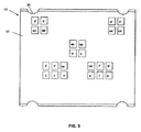
図2〜図6を参照すると、本発明の1つの実施形態は、ジャック44を含み、これはPCB52、正面不伝導性フレーム54、背面不伝導性フレーム56、垂直PCB金属摺動体58、垂直バネ60、プラグインターフェース接点(PIC)61(4、5)、PIC62(1、2、3、6、7、8)、PIC63(3’、4’、5’、6’)、絶縁変位接点(IDC)64、水平金属分割具66、垂直金属分割具67および金属ジャック筐体68を有するものである。ジャック44はワイヤキャップ、引張軽減クリップおよび他のケーブル、導体コネクタ装置をも含むことが可能である。
2-6, one embodiment of the present invention includes a
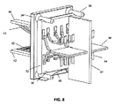
要素52、54、56、58、60、61、62、63の組み合わせである、ジャック44内の切替機構65は、図7に示されるように、RJ45プラグ46およびIEC60603−7−71プラグ70準拠の二元機能性を提供し、そして垂直自由度を有する摺動PCB52およびRJ45およびIEC60603−7−71のためのPCB52における2つの独立回路100、102を有する連結回路、(これらは図3、図4、図5、および図6に示される)、を組み込むことによって達成される。摺動PCB52は、挿入されたプラグに基づいてPCB52の位置決めを援助するバネ要素60の上に乗る。さらに、PCB52は不伝導性フレーム(表面54および背面56)間に拘束される。不伝導性フレーム54、56は整列機能84、88ならびにPCB52内の付き合わせ機能86を有し、PCB52をZ方向に拘束するのを援助し、プラグ46、70の挿入および引き抜き時にPCB52に関する最大垂直移動(−Yおよび+Y方向)を限定するための一方向をも提供する。ジャックに挿入されるプラグの型式に基づき、プラグ46またはプラグ70、PCB52は、ジャック接点61、62、および63とPCB52上の2つの独立回路100、102の1つとの間の信号経路の切り替えを可能とする2つの可能な場所の1つに配置される。
The
ジャック44は12個のプラグインターフェース接点を提供されており、それらはPIC61(接点4、5),PIC62(接点1、2、3、6、7、8)およびPIC63(接点3’、4’、5’、6’)で、PCB52の正面側の対応する接点パッドおよびプラグ46または70の接点と整合されるように固定正面不伝導性フレーム54によって所定位置に保持される。正面不伝導性フレーム54は、突出したカンチレバー型特徴部80、82をも有し、これらはプラグ接点と係合された状態でPIC61、62、63を支持する。カンチレバー型特徴部80、82は、挿入および係合時にPIC61、62、63のための追加垂直力を提供するのを助ける。PIC1〜8(61、62)は従来型RJ45プラグと嵌め合うような形で取りまとめられる。図7に示されるIEC60603−7−71様式プラグ70は、接点対間のより多くの分離を創生し、また各対間の遮蔽体73を提供することによって、RJ45プラグ46と比較して、4対間のより多くの隔離を提供するように設計されている。
The
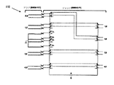
図7および13を参照すると、切替機構は、IEC60603−7−71プラグの正面の鼻特徴部71によって、IEC60603−7−71プラグ70の挿入中に活性化される。プラグ70を挿入すると、PCB52は摺動し、これはジャック44内のPIC61、62、63を通るプラグ接点間の信号経路をPCB52上の2つの異なる回路100、102の1つに切り替える。図5および図6の概略図は、ジャック44に挿入されるプラグの型式、46または70に基づく切り替え可能回路接続を示す。図5を参照すると、動作のRJ45モード中に利用される1つの回路100は、プラグ46がジャック44に挿入されたとき、図4に示されるように、PCB52の背面表面55上の接点パッド1〜8を接続し、図3に示されるように、PCB52の正面表面57上の接点パッド1〜8を分離する。図6を参照すると、PCB52上の第2の回路102が、IEC60603−7−71プラグ70がジャック44に挿入されたときに利用され、図4に示されるように、PCB52の背面表面55上の接点パッド1’〜8’を接続し、図3に示されるように、PCB52の正面表面57上の接点パッド1’〜8’を分離する。図2を参照すると、IDC64はジャック44までの撚り線対ケーブルを終端させるための手段を提供し、固定背面不伝導性フレーム56によって所定位置に保持されてPCB52との整合を維持する。PCB52の背面側との接続は、図4に示されるように、メッキ済み貫通穴または接点パッドまでトレースによって接続されるバイアによって行われる。PCB52の背面側上では、適切なバイアまでトレースによって接続される追加接点パッドが、8個のIDC64と整合するように位置決めされる。2つの独立した回路100、102において、どの接点パッド間においても接続の共通点はない。接地パッド3G’、4G’、5G’、および6G’はPCB52の背面表面55上に配置され、動作のRJ45モード中に不使用PIC63(3’、4’、5’、および6’)を接地する。接地パッド3G、4G、5G、および6Gは、PCB52の背面表面55上に配置され、動作のIEC60603−7−71モード中に不使用PIC(3、4、5、および6)を接地する。PCB52の正面表面57上の接地パッドは、動作のいずれかのモード中に金属分割具66、67の接地方法を提供する。
7 and 13, the switching mechanism is activated during insertion of the IEC 60603-7-71
プラグ46またはプラグ70のいずれかからの適切なプラグ接点をIDC64に接続するために互いに隔離された、2つの完全に独立した回路100、102を使用することにより、動作のRJ45モード中に必要とされる補償回路は、IEC60603−7−71モードで動作中にジャック44の電気的性能に衝撃を与えない。各回路100、102のこの隔離は、ジャック44の広帯域幅性能目標を満たそうとするときに利点がある。2つの独立した回路100、102を使用することにより、切り替え中にPCB52の摺動行為と連結され、IDC64は、それぞれRJ45プラグ46およびIEC60603−7−71プラグ70専用の接点パッド1〜8、1’〜8’の別々のセットと接触するようになる。
Required during RJ45 mode of operation by using two completely
図2を参照すると、PIC(61、62および63)、IDC(64)および金属分割具(66、67)は、その脚端においてバネ特性90、92、94、96、98を有する様に設計され、したがって、摺動PCB52との払拭接点を有しながら、接点パッド上に一定の力を有する。PIC61は、PIC62とは異なる位置および向きにおいてPCB52と係合する。PIC62に対するこのPIC61の取りまとめは、RJ45モードで動作時に、対36および45間のジャック内のあらゆる追加混信を最小化するのに役立つ。
Referring to FIG. 2, the PIC (61, 62 and 63), IDC (64) and metal divider (66, 67) are designed to have
4信号対間の隔離を維持するため、またIDC64とワイヤ対間の望まない混信を阻止するため、水平66および垂直金属分割具67が組み立てられ、IDC64の4対間に位置決めされる。金属分割具66、67のこの取りまとめは、各ワイヤ対に関する四分円の形成を可能とする。金属分割具66、67は、4ワイヤ対のそれぞれの周りに包まれる個々の金属箔遮蔽体を接地する1つの方法も提供する。図8を参照すると、金属分割具66、67をPCB52に接地することにより、ケーブル遮蔽体の連続性ならびに個々の対遮蔽体が確立可能である。組み立て品全体が金属ジャック筐体68内に挿入され、これはまた金属ジャック全体についてケーブル間の遮蔽体の連続性ならびにプラグ接続性を維持するのにも役立つ。
In order to maintain isolation between the four signal pairs and to prevent unwanted interference between the
図9〜12を参照すると、動作中は、ジャック44にプラグが何も挿入されていないとき(「アイドル状態」)、バネ要素60は、PCB52の整合特徴部86が不伝導性フレーム54、56上の対応する位置決め特徴部84、88と係合するまで、PCB52’を上方向へ強いる。PCB52がこの位置にあって、PCB52の正面側の接点パッド1〜8は固定PIC(61、62)1〜8と整合される。さらに、PCB52の背面側のIDC接点パッド1〜8は、図10および11に示されるように、固定IDC(64)1〜8と整合される。このアイドル状態にある間、8つのRJ45接点61、62は8つのIDC64とPCB52を介して接続される。
Referring to FIGS. 9-12, in operation, when no plug is inserted into the jack 44 (“idle state”), the
RJ45プラグ46が、図11に図解されるように、ジャック44に挿入されると、切替機構は活性化されない。プラグ接点はジャック44内の固定接点(61、62)1〜8と係合し、それにより、プラグ46とジャック44の他方端上のIDC64内で終端されるケーブルとの間の連続性を確立する。CAT6A等のRJ45ジャックにおいて一般的なように、RJ45プラグ内に存在する固有の混信を打ち消すために混信補償が必要である。この補償回路は、図5に概略的に示されるC13、C35、C46およびC68等の導体間の離散および/または分配容量性および誘電性要素を含み得るものであるが、PCB52の内部および/または外部上に実現可能である。反射減衰量、遠端混信(FEXT)、平衡性等を最適化するのに役立つ他の補償要素も含まれることが可能である。ジャック44がRJ45プラグ46と係合されている間、PCB52は、8つのRJ45プラグ接点61、62とケーブル導体を終端する8つのIDC64との間の連続性を提供する形で位置決めされる。他の固定PIC63、3’、4’、5’、および6’は、ジャック44内の各対間の意図しない連結および混信を導入する可能性がある。この意図しない連結および混信が発生するのを阻止するため、これらの導体63は、図12に示されるように、PCB52の正面側の適切に配置された接地パッドを通して、PCB52に接地される。
When the
図13を参照すると、IEC60603−7−71様式プラグ70がジャック44に挿入されたとき、プラグの正面上の鼻特徴部71はPCB52にマウントされたPCB摺動体58と係合する。プラグ70がジャック44にさらに挿入されるにつれ、鼻特徴部71は摺動体58の角度のついた面に対して力と変位を提供する。摺動体58は摺動体58の傾斜に基づき、変位をPCB52に転送する。この設計では、PCB52の変位は水平方向に沿って不伝導性フレーム(54および56)により提供される拘束のゆえにY方向に変換される。その結果、鼻特徴部71の挿入と共にPCB52は下方向に移動する間、PCB52の底部表面はバネ60を押す。PCB52からの力の垂直構成要素がバネ力より大きいときは、PCB52は下方向に摺動し、プラグ70がその最終位置に挿入されるまでバネ要素60を反らせる。この行為は、ステップS10(プラグ接近)、S12(初期プラグ接触)、S14(PCB52の摺動行為)、およびS16(最終係合位置)と共に図13に図解される。摺動体58は変位をPCB52に転送する形で設計され、一方、バネに類似する特性100も有して、必要な垂直変位が発生したときに部品のいくつかの許容値および動きを提供する。
Referring to FIG. 13, when an IEC 60603-7-71
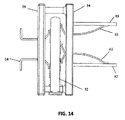
図14および15を参照すると、PCB52の正面と係合する12の固定PIC(61、62および63)ならびにPCB52の背面と係合する8つの固定IDC接点64は、PCB52が下方向に摺動するように強いられるにつれ、RJ45接点パッドから接続を絶たれる。プラグがいっぱいに挿入されると、PCB52はその最終位置まで下方向に摺動する。この位置において、12のPICと8つの固定IDCは、図14および図15に見られるように、PCB52の正面および背面側の異なる接点パッドとこの時点で整合される。PCB52が移動するにつれ、PIC61、62、63はそれぞれの接点パッドを摺動によりオフおよびオンとする。PCB52の接点パッドの摺動によるオンおよびオフのプロセスにおいて、PCB52の接点パッドの表面上に存在し得るあらゆる汚染物または酸化物は払拭され、それにより、PIC61、62、63、IDC64、およびPCB52間の強固な気密接続を確保する。
14 and 15, the twelve fixed PICs (61, 62 and 63) that engage the front of the
動作のIEC60603−7−71モードにおいてすべての12の固定PIC61、62、63および8つの固定IDC64を新しい接点パッドに接続することによって、動作のRJ45モードのために必要であったPCB52上のすべての補償回路が全4つの信号対上の信号経路から完全に切り離される。さらに、PIC3、4、5、および6はPCB52の正面側の接地パッドに接続される。不使用のPIC3、4、5、および6を接地することは、十分な反射減衰量、挿入損失、およびより高い周波数における電気的平衡性能を達成するうえで利点がある。
By connecting all 12 fixed
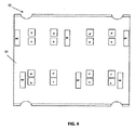
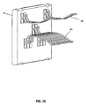
図16を参照すると、1つの実施形態に従って、第2のジャック45は2つのステージ補償のための設備を含む。広い十分な帯域幅にわたってRJ45プラグの混信を十分に補償するためには、2ステージの回路を実装することが必要であろう。例えば、CAT6A標準は500MHzの周波数までの混信要件を指定する。2ステージの補償が必要となった場合には、第2のPCB72を水平構成内に組み込み可能である。図16はジャック45の分解図で、垂直PCB53、正面不伝導性フレーム59、背面不伝導性フレーム56、垂直PCB金属摺動体58、垂直バネ60、PIC1〜8(PIC61、62)、PIC(3’、4’、5’、6’)63、IDC64、水平金属分割部66、垂直金属分割部67、および金属ジャック筐体68、不伝導性摺動体74、ジャック筐体69、水平PCB72および水平バネ76、を備える。
Referring to FIG. 16, according to one embodiment, the
ジャック45の動作中、補償回路の第1のステージは、PCB72上に配置可能であり、一方、第2の補償ステージはPCB53上に配置可能である。バネ要素76は、図17に示されるように、PCB72を、固定PIC(61、62)1〜8をPCB72の頂面側の対応する接点パッドと整合させるために、適切な位置(RJ45プラグ46インターフェースについて)に強いる。適切な補償回路は、これは導体間の不伝導性および/または分配容量性および誘導性要素を含み得るが、図18に示されるように、PCB72の内部および/または外部層上に実現可能である。
During operation of
図17〜19を参照すると、もしも補償の2つのステージがPCB72およびPCB53を介して動作のRJ45モードにおいて必要とされる場合には、補償回路の両ステージは全4信号対から切り離される必要がある。補償回路のこの切り離しを達成するには、固定PICのPCB72への接続は、動作のIEC60603−7−71モードのために変更されねばならない。
Referring to FIGS. 17-19, if two stages of compensation are required in the RJ45 mode of operation via
図16および図19を参照すると、PCB53にマウントされた2つの不伝導性摺動体74が、IEC60603−7−71プラグ70が挿入されたときにPCB53が下方向へ摺動するように強いられると、PCB72と係合するように設計される。PCB72はY方向に移動することを拘束され、バネ要素76がZ方向に沿う動きに抗し、Z方向はわずかな程度となる。プラグ70が挿入されると、PCB53は下方向に摺動するように強いられ(S18)、これは不伝導性摺動体74がPCB72に対して力を適用し、変位させるようにする。不伝導性摺動体74の傾斜性質およびPCB72に関するY方向における拘束の理由で、PCB53の下方向変位(S18)は、バネ76に対するZ方向へ変換される。この水平力がバネ要素76の対抗力より大きいときは、PCB72は横方向に摺動し(S20)、プラグ70がその最終位置に挿入されるまでバネ要素76を圧縮する。PCB72の頂部表面と係合する8つのPIC61、62は、PCB72が横方向に摺動するように強いられると、対応するRJ45接点パッドから切り離される。プラグ70がジャック45内にいっぱいに挿入されると、PCB72はその最終位置まで横方向に摺動する。この位置において、8つのPIC61、62はPCB72の頂部側の異なる接点パッドと今度は整合される。PIC1、2、7、および8はPCB72上の補償回路とはもはや接続はなく、PIC3、4、5、および6は、図20に示されるように、PCB72の頂部側の接地パッドと今度は接続される。これらの信号接地パッドは、十分な反射減衰量、挿入損失、およびより高い周波数における電気的平衡性能を達成する上において利点がある。
Referring to FIGS. 16 and 19, when two
PCB53、72の摺動行為は、これはIEC60603−7−71プラグ70の正面上の鼻特徴部71によって活性化されるが、本質的にはPCB53、72上の2つの異なる回路間の嵌め合い接続性を通して信号経路を切り替える。図6はIEC60603−7−71プラグ70がジャックに挿入されたときに切り替え可能回路接続を図式的に示す。
The sliding action of the
本発明に従う2つの追加実施形態が図21〜24に示されている。図21(RJ45モード)および図22(IEC60603−7−71モード)に示される1つの実施形態では、PCB75は、追加接点77(0および9接点)により、ジャック44内のPCB52の代理をし得る。図23(RJ45モード)および図24(IEC60603−7−71モード)に示される別の実施形態では、追加接点77(0および9接点)により、PCB79は、ジャック45内のPCB53の代理が可能で、PCB78はジャック45内PCB72の代理が可能である。図21〜24に示される実施形態は、本発明に従うジャック44、45の電気的整合を、より具体的には、追加接点77(0および9接点)、ジャック44または45のいずれかがIEC60603−7−71モードで動作時に、改善可能である。
Two additional embodiments according to the present invention are shown in FIGS. In one embodiment shown in FIG. 21 (RJ45 mode) and FIG. 22 (IEC 60603-7-71 mode),
図21〜24に示される実施形態では、IEC60603−7−71モードで動作時に、PIC(62)1および2は、IEC60603−7−71プラグ上の対応する接点と嵌め合わされ、そしてPIC3は接地される。PIC3の位置がPIC2に隣接すると、インピーダンスの不連続性が生じる。PIC1の偶数および奇数モードインピーダンスは、生得的にPIC2より高い。このインピーダンス不連続性は、このインターフェースにおける電気的反射の増加ならびにモード変換の増加に帰結する。対12の差分反射減衰量、挿入損失、および混信性能は、ジャックのこの生得的条件のゆえにすべて劣化される。これらの性能劣化を避けるために、PIC1および2の偶数および奇数モードインピーダンスは、ケーブルの特性インピーダンスと等しく、そして一致されるべきである。接点0(77)を導入することによって、これは動作のIEC60603−7−71モードで接地されるが、PIC1(62)に隣接してインピーダンスは等しくなる。これは接地導体および信号導体(G−S−S−G)の平衡構成を提供し、そしてこの平衡送信線構成は、帯域幅が増加するにつれ、信号健全性に対してより利点を有する。
In the embodiment shown in FIGS. 21-24, when operating in IEC 60603-7-71 mode, PIC (62) 1 and 2 are mated with corresponding contacts on the IEC 60603-7-71 plug, and
動作のIEC60603−7−71モードにおいて、類似した懸念がPIC7および8に存在する。PIC7および8はその対応するプラグ接点と嵌め合わされ、PIC6は接地される。PIC6がPIC7に隣接しているため、PIC8の偶数および奇数モードインピーダンスは生得的にPIC7より高い。追加接地接点9(77)をPIC8(62)に隣接して追加することにより、平衡G−S−S−G構成が創生され、性能劣化が回避または最小化される。プラグ70の挿入時にPCB75が下方向へ摺動するとき、実施形態3の場合は、接点0および9(77)はPCB75上の接点パッドを通して接地され、また実施形態4の場合は、接点0および9(77)は、プラグ70の挿入時にPCB79が下方向へ摺動するとき、PCB79、78上の接点パッドを通して接地される。接点77(0および9)の固定位置は、PIC1〜8に対してわずかにずらされ、プラグ本体が0および9接点77と干渉せずに十分に挿入されることを可能とする。このずれがなければ、プラグ本体の堅固な部分はPICの形状と干渉して変形させるであろう。プラグ本体は0および9接点77を遮蔽できるように修正も可能である。
Similar concerns exist in PICs 7 and 8 in the IEC 60603-7-71 mode of operation. PICs 7 and 8 are mated with their corresponding plug contacts and
接点77(0および9)の別の可能な使用法は、ジャック44または45がRJ45モードにおいて動作しているときに必要とされる混信補償回路に組み込むことである。これらは、対12および対78に連結する対36の分離によって引き起こされるスーパーペア効果を最小化する追加の方法を提供し得る。
Another possible use of contact 77 (0 and 9) is to incorporate into the interference compensation circuit required when
本明細書中に記述される目的物は、ときどき、異なる他の構成要素に含まれる、または接続される、異なる構成要素を図解する。そのような描写された構造は単に例題的であり、また、実際同一の機能性を達成する多くの他の構造を実装可能であることが理解されるべきである。概念的意味においては、同一機能性を達成するための構成要素のどの取りまとめも、希望する機能性が達成されるように効果的に「関係づけられている」。このゆえに、特定機能性を達成するために本明細書中で組み合わされたどの2つの構成要素も、希望する機能性が達成されるように、構造または中間構成要素に関わらず、互いに「関係している」と見られることが可能である。同様に、その様に関連付けられたどの2つの構成要素も、希望する機能性が達成するために、互いに「動作可能に接続された」または「動作可能に連結された」として見られることも可能であり、そのように関連付けられることが可能などの2つの構成要素も、希望する機能性が達成するために、互いに「動作可能に連結可能」として見られることが可能である。動作可能に組み合わせ可能の具体例は、これらに限定されないが、物理的に嵌め合い可能なおよび/または物理的に相互作用可能な構成要素、および/または、無線で相互作用可能なおよび/または無線で相互作用している構成要素、および/または、論理的に相互作用しているおよび/または論理的に相互作用可能な構成要素を含む。 Objects described herein illustrate different components that are sometimes included or connected to different other components. It should be understood that such depicted structure is merely exemplary and that many other structures that in fact achieve the same functionality can be implemented. In a conceptual sense, any compilation of components to achieve the same functionality is effectively “associated” so that the desired functionality is achieved. Thus, any two components combined herein to achieve a particular functionality are “relevant” to each other, regardless of structure or intermediate components, so that the desired functionality is achieved. Can be seen. Similarly, any two components so associated can be viewed as “operably connected” or “operably linked” to each other to achieve the desired functionality. Any two components that can be so associated can be viewed as “operably connectable” to each other to achieve the desired functionality. Examples of operably combinable include, but are not limited to, physically fitable and / or physically interactable components, and / or wirelessly interactable and / or wireless And / or components that are logically interacting and / or capable of logical interaction.
本開示の要約書は、読者が技術的開示の性質を素早く確かめるのを可能とするために提供されている。それが請求項の範囲または意味を解釈または限定するために使用されないという理解のもとで提出されている。さらに、先行する発明を実施するための形態においては、本開示を整理する目的のために、さまざまな実施形態においてさまざまな特徴がグループ化されているのを見ることができる。開示のこの方法は、各請求項において明示的に記載されたより多くの特徴を、請求された実施形態が必要とする、という意図を反映するものとして解釈されるべきではない。むしろ、以下の請求項が反映するように、発明の目的物は単一開示実施形態の全特徴より少なく存在する。このように、以下の請求項はこれにより「発明を実施するための形態」に組み込まれ、それぞれの請求項は別々に請求される目的物として独立している。 A summary of this disclosure is provided to enable the reader to quickly ascertain the nature of the technical disclosure. It is submitted with the understanding that it will not be used to interpret or limit the scope or meaning of the claims. Furthermore, in the preceding detailed description, it can be seen that various features are grouped in various embodiments for the purpose of organizing the present disclosure. This method of disclosure is not to be interpreted as reflecting an intention that the claimed embodiments require more features than are expressly recited in each claim. Rather, the subject matter of the invention is present in less than all features of a single disclosed embodiment, as reflected in the following claims. Thus, the following claims are hereby incorporated into the Detailed Description, with each claim standing on its own as a separately claimed object.
発明のさまざまな実施形態が記述されてきたが、本発明の範囲の中で他の実施形態および実装が可能であることは当業者にとっては明白であろう。したがって、本発明は付属請求項およびその同等物に基づく場合を除き、限定されるべきではない。 While various embodiments of the invention have been described, it will be apparent to those skilled in the art that other embodiments and implementations are possible within the scope of the invention. Accordingly, the invention should not be limited except as by the appended claims and their equivalents.
1〜8 接点パッド
3G、4G、5G 接地パッド
40 銅構造化配線通信システム
42 パッチパネル
44、45 ジャック
46、70 プラグ
48、50 ケーブル
54 正面不伝導性フレーム
56 背面不伝導性フレーム
58 金属摺動体
60 垂直バネ
61、62 接点
63 導体
64 絶縁変位接点(IDC)
65 切替機構
66 水平金属分割具
67 垂直金属分割具
68 金属ジャック筐体
71 鼻特徴部
80、82 カンチレバー型特徴部
86 整合特徴部
1-8 Contact pads 3G, 4G,
65
Claims (8)
プラグ受容開口を含む筐体と、
前記プラグ受容開口内のプラグインターフェース接点の第1のセットと、
前記プラグ受容開口内のプラグインターフェース接点の第2のセットであって、プラグインターフェース接点の前記第2のセットはプラグインターフェース接点の前記第1のセットのいくつかを含むところの、第2のセットと、
ケーブル接続接点のセットと、
少なくとも部分的には前記筐体内にあるプリント基板(PCB)であって、前記PCBは第2の回路から隔離された第1の回路を含み、前記PCBはバネによって動くように少なくとも第1の位置および第2の位置を備える前記筐体内に摺動可能に構成されるところの、PCBと、
を備え、
前記第1の位置において、前記第1の回路はプラグインターフェース接点の前記第1のセットに直接的に接続され、かつケーブル接続接点の前記セットに直接的に接続され、前記第1の回路はプラグインターフェース接点の前記第1のセットをケーブル接続接点の前記セットに接続し、
前記第2の位置において、前記第2の回路はプラグインターフェース接点の前記第2のセットに直接的に接続され、かつケーブル接続接点の前記セットに直接的に接続され、前記第2の回路はプラグインターフェース接点の前記第2のセットをケーブル接続接点の前記セットに接続する、
通信コネクタ。 A communication connector,
A housing including a plug receiving opening;
A first set of plug interface contacts in the plug receiving opening;
A second set of plug interface contacts in the plug receiving opening, wherein the second set of plug interface contacts includes some of the first set of plug interface contacts; ,
A set of cable connection contacts;
A printed circuit board (PCB) at least partially within the housing, wherein the PCB includes a first circuit isolated from a second circuit, the PCB being moved by a spring at least in a first position. And a PCB configured to be slidable within the housing having a second position;
With
In the first position, the first circuit is directly connected to the first set of plug interface contacts and is directly connected to the set of cable connection contacts, the first circuit being plugged Connecting the first set of interface contacts to the set of cable connection contacts;
In the second position, the second circuit is directly connected to the second set of plug interface contacts and is directly connected to the set of cable connection contacts, the second circuit being plugged Connecting the second set of interface contacts to the set of cable connection contacts;
Communication connector.
通信装具と、
前記通信装具に接続される通信コネクタと、を備え、
前記通信コネクタは、
プラグ受容開口を含む筐体と、
前記プラグ受容開口内のプラグインターフェース接点の第1のセットと、
前記プラグ受容開口内のプラグインターフェース接点の第2のセットであって、プラグインターフェース接点の前記第2のセットはプラグインターフェース接点の前記第1のセットのいくつかを含むところの、第2のセットと、
ケーブル接続接点のセットと、
少なくとも部分的には前記筐体内にあるプリント基板(PCB)であって、前記PCBは第2の回路から隔離された第1の回路を含み、前記PCBはバネによって動くように少なくとも第1の位置と第2の位置を有する前記筐体内に摺動可能に構成されるところの、PCBとを備え、
前記第1の位置において、前記第1の回路はプラグインターフェース接点の前記第1のセットに直接的に接続され、かつケーブル接続接点の前記セットに直接的に接続され、前記第1の回路はプラグインターフェース接点の前記第1のセットをケーブル接続接点の前記セットに接続し、
前記第2の位置において、前記第2の回路はプラグインターフェース接点の前記第2のセットに直接的に接続され、かつケーブル接続接点の前記セットに直接的に接続され、前記第2の回路はプラグインターフェース接点の前記第2のセットをケーブル接続接点の前記セットに接続する、
通信システム。 A communication system,
Communication equipment,
A communication connector connected to the communication device,
The communication connector is
A housing including a plug receiving opening;
A first set of plug interface contacts in the plug receiving opening;
A second set of plug interface contacts in the plug receiving opening, wherein the second set of plug interface contacts includes some of the first set of plug interface contacts; ,
A set of cable connection contacts;
A printed circuit board (PCB) at least partially within the housing, wherein the PCB includes a first circuit isolated from a second circuit, the PCB being moved by a spring at least in a first position. And a PCB configured to be slidable in the housing having the second position,
In the first position, the first circuit is directly connected to the first set of plug interface contacts and is directly connected to the set of cable connection contacts, the first circuit being plugged Connecting the first set of interface contacts to the set of cable connection contacts;
In the second position, the second circuit is directly connected to the second set of plug interface contacts and is directly connected to the set of cable connection contacts, the second circuit being plugged Connecting the second set of interface contacts to the set of cable connection contacts;
Communications system.
プラグ受容開口を含む筐体と、
前記プラグ受容開口内のプラグインターフェース接点の第1および第2のセットであって、プラグインターフェース接点の前記第2のセットはプラグインターフェース接点の前記第1のセットの少なくとも1対を含む、第1および第2のセットと、
前記第1のプラグが前記プラグ受容開口内に挿入されたときに、プラグインターフェース接点の前記第1のセットと係合する第1の回路と、前記第2のプラグが前記プラグ受容開口内に挿入されたときにプラグインターフェース接点の前記第2のセットと係合する第2の回路とを有する、連結回路と、
前記筐体内に配置され、前記連結回路が形成された回路板と、を備え、
前記回路板は、前記第1の回路がプラグインターフェース接点の前記第1のセットと係合する第1の位置と、前記第2の回路がプラグインターフェース接点の前記第2のセットと係合する第2の位置との間をバネによって移動可能である、通信ジャック。 A communication jack for connection with one of the first plug and the second plug,
A housing including a plug receiving opening;
First and second sets of plug interface contacts in the plug receiving opening, wherein the second set of plug interface contacts includes at least one pair of the first set of plug interface contacts; A second set;
A first circuit that engages the first set of plug interface contacts when the first plug is inserted into the plug receiving opening; and the second plug is inserted into the plug receiving opening. A coupling circuit having a second circuit engaged with the second set of plug interface contacts when
A circuit board disposed in the housing and having the connection circuit formed thereon ,
The circuit board includes a first position where the first circuit engages the first set of plug interface contacts, and a second position where the second circuit engages the second set of plug interface contacts. A communication jack that can be moved between two positions by a spring.
Applications Claiming Priority (5)
| Application Number | Priority Date | Filing Date | Title |
|---|---|---|---|
| US201161543866P | 2011-10-06 | 2011-10-06 | |
| US61/543,866 | 2011-10-06 | ||
| US13/632,211 US8944855B2 (en) | 2011-10-06 | 2012-10-01 | Backward compatible connectivity for high data rate applications |
| US13/632,211 | 2012-10-01 | ||
| PCT/US2012/058389 WO2013052436A2 (en) | 2011-10-06 | 2012-10-02 | Backward compatible connectivity for high data rate applications |
Publications (3)
| Publication Number | Publication Date |
|---|---|
| JP2014531732A JP2014531732A (en) | 2014-11-27 |
| JP2014531732A5 JP2014531732A5 (en) | 2015-10-29 |
| JP5893744B2 true JP5893744B2 (en) | 2016-03-23 |
Family
ID=48042366
Family Applications (1)
| Application Number | Title | Priority Date | Filing Date |
|---|---|---|---|
| JP2014534630A Expired - Fee Related JP5893744B2 (en) | 2011-10-06 | 2012-10-02 | Backward compatible connectivity for high data rate applications |
Country Status (5)
| Country | Link |
|---|---|
| US (3) | US8944855B2 (en) |
| EP (1) | EP2764585B1 (en) |
| JP (1) | JP5893744B2 (en) |
| CN (1) | CN103931058B (en) |
| WO (1) | WO2013052436A2 (en) |
Families Citing this family (16)
| Publication number | Priority date | Publication date | Assignee | Title |
|---|---|---|---|---|
| US8715012B2 (en) * | 2011-04-15 | 2014-05-06 | Adc Telecommunications, Inc. | Managed electrical connectivity systems |
| CN102957056B (en) * | 2011-08-19 | 2015-02-25 | 富士康(昆山)电脑接插件有限公司 | Electric coupler |
| US8939798B2 (en) * | 2011-12-12 | 2015-01-27 | Commscope, Inc. Of North Carolina | Local area networks for intelligent patching system controllers and related methods, controllers and communications interfaces |
| US9531135B2 (en) * | 2013-03-15 | 2016-12-27 | CommScope Connectivity Spain, S.L. | Telecommunications jack with switchable circuit configurations |
| EP3024098A2 (en) | 2013-07-15 | 2016-05-25 | TE Connectivity AMP España S.L.U. | Telecommunications plug connector for high data rate uses |
| US9419391B2 (en) * | 2013-08-20 | 2016-08-16 | Panduit Corp. | Communication connector |
| US10559927B2 (en) * | 2013-10-11 | 2020-02-11 | Panduit Corp. | Switchable RJ45/ARJ45 jack |
| EP3055906B1 (en) * | 2013-10-11 | 2019-05-15 | Panduit Corp. | Switchable rj45/arj45 jack |
| US9559476B2 (en) * | 2014-05-09 | 2017-01-31 | Panduit Corp. | ARJ45 to RJ45 adapter |
| US10050383B2 (en) | 2015-05-19 | 2018-08-14 | Panduit Corp. | Communication connectors |
| US20170256895A1 (en) * | 2016-03-02 | 2017-09-07 | Panduit Corp. | Communication connector |
| US9985373B2 (en) * | 2016-10-12 | 2018-05-29 | Surtec Industries, Inc. | Communication connector |
| US10361514B2 (en) * | 2017-03-02 | 2019-07-23 | Panduit Corp. | Communication connectors utilizing multiple contact points |
| CN108258469A (en) * | 2017-12-29 | 2018-07-06 | 曙光信息产业(北京)有限公司 | A kind of realization system of the network port |
| CN111193124B (en) * | 2018-11-15 | 2021-07-27 | 泰科电子(上海)有限公司 | Electrical connector |
| DE102019127134A1 (en) * | 2019-10-09 | 2021-04-15 | Perinet GmbH | Plug for an Internet of Things device |
Family Cites Families (24)
| Publication number | Priority date | Publication date | Assignee | Title |
|---|---|---|---|---|
| US3354355A (en) | 1966-10-24 | 1967-11-21 | Beckman Instruments Inc | Mode selection switch |
| US4679879A (en) * | 1986-10-03 | 1987-07-14 | Molex Incorporated | Plug and receptacle connector assembly |
| US5186647A (en) * | 1992-02-24 | 1993-02-16 | At&T Bell Laboratories | High frequency electrical connector |
| US5647767A (en) * | 1995-02-06 | 1997-07-15 | The Whitaker Corporation | Electrical connector jack assembly for signal transmission |
| FR2733350B1 (en) | 1995-04-19 | 1997-06-06 | Connexion Soc Nle | MINIATURE COAXIAL SWITCH OR INVERTER CONNECTOR WITH PRINTED CIRCUIT BOARD |
| US6079996A (en) | 1999-04-15 | 2000-06-27 | Lucent Technologies Inc. | Selectable compatibility electrical connector jack |
| US7021971B2 (en) | 2003-09-11 | 2006-04-04 | Super Talent Electronics, Inc. | Dual-personality extended-USB plug and receptacle with PCI-Express or Serial-At-Attachment extensions |
| US6156981A (en) | 1999-08-06 | 2000-12-05 | Thomas & Betts International, Inc. | Switch for data connector jack |
| US6244908B1 (en) | 2000-08-04 | 2001-06-12 | Thomas & Betts International, Inc. | Switch within a data connector jack |
| US6739912B2 (en) * | 2001-11-08 | 2004-05-25 | Hon Hai Precision Ind. Co., Ltd. | Modular jack assembly having improved positioning means |
| US6736681B2 (en) * | 2002-10-03 | 2004-05-18 | Avaya Technology Corp. | Communications connector that operates in multiple modes for handling multiple signal types |
| US7182649B2 (en) * | 2003-12-22 | 2007-02-27 | Panduit Corp. | Inductive and capacitive coupling balancing electrical connector |
| US7044750B1 (en) * | 2005-07-12 | 2006-05-16 | U.D. Electronic Corp. | Network connector |
| US8182294B2 (en) | 2007-05-07 | 2012-05-22 | Ortronics, Inc. | Connector assembly and related methods of use |
| US7628657B2 (en) * | 2007-05-07 | 2009-12-08 | Ortronics, Inc. | Connector assembly for use with plugs and preterminated cables |
| US7828569B2 (en) * | 2007-09-17 | 2010-11-09 | Finisar Corporation | Receptacle with multiple contact sets for different connector types |
| US7956618B2 (en) | 2007-10-31 | 2011-06-07 | Sony Ericsson Mobile Communications Ab | Additional pins on a USB connector |
| WO2009100296A1 (en) | 2008-02-08 | 2009-08-13 | Panduit Corp. | Communications connector with improved contacts |
| CN201207652Y (en) * | 2008-03-25 | 2009-03-11 | 富士康(昆山)电脑接插件有限公司 | Network interface circuit and electric connector having the circuit |
| TWM379191U (en) | 2008-12-03 | 2010-04-21 | Hon Hai Prec Ind Co Ltd | Electrical connector |
| CN101877448B (en) * | 2009-04-29 | 2012-11-28 | 富士康(昆山)电脑接插件有限公司 | Module connector |
| US7993166B1 (en) | 2010-06-01 | 2011-08-09 | Hon Hai Precision Ind. Co., Ltd. | Hybrid modular jack |
| WO2012054345A1 (en) * | 2010-10-22 | 2012-04-26 | Adc Telecommunications, Inc. | Contact set arrangement for right angle jack |
| US8715012B2 (en) * | 2011-04-15 | 2014-05-06 | Adc Telecommunications, Inc. | Managed electrical connectivity systems |
-
2012
- 2012-10-01 US US13/632,211 patent/US8944855B2/en active Active
- 2012-10-02 CN CN201280056171.5A patent/CN103931058B/en active Active
- 2012-10-02 EP EP12780341.9A patent/EP2764585B1/en active Active
- 2012-10-02 WO PCT/US2012/058389 patent/WO2013052436A2/en active Application Filing
- 2012-10-02 JP JP2014534630A patent/JP5893744B2/en not_active Expired - Fee Related
-
2015
- 2015-01-29 US US14/608,695 patent/US9698547B2/en not_active Expired - Fee Related
-
2017
- 2017-06-30 US US15/639,239 patent/US9876322B2/en not_active Expired - Fee Related
Also Published As
| Publication number | Publication date |
|---|---|
| WO2013052436A3 (en) | 2013-07-04 |
| CN103931058B (en) | 2017-03-08 |
| JP2014531732A (en) | 2014-11-27 |
| US20130090011A1 (en) | 2013-04-11 |
| EP2764585A2 (en) | 2014-08-13 |
| WO2013052436A2 (en) | 2013-04-11 |
| CN103931058A (en) | 2014-07-16 |
| US9876322B2 (en) | 2018-01-23 |
| US8944855B2 (en) | 2015-02-03 |
| EP2764585B1 (en) | 2016-08-17 |
| US20150171576A1 (en) | 2015-06-18 |
| US20170302038A1 (en) | 2017-10-19 |
| US9698547B2 (en) | 2017-07-04 |
Similar Documents
| Publication | Publication Date | Title |
|---|---|---|
| JP5893744B2 (en) | Backward compatible connectivity for high data rate applications | |
| US9419391B2 (en) | Communication connector | |
| US8052483B1 (en) | Communication connector with improved crosstalk connection | |
| US7967645B2 (en) | High speed data communications connector circuits, systems, and methods for reducing crosstalk in communications systems | |
| US9246285B2 (en) | Network jack with backwards capability and systems using same | |
| US9246274B2 (en) | Communication connectors having crosstalk compensation networks | |
| US7976349B2 (en) | Communications patching and connector systems having multi-stage near-end alien crosstalk compensation circuits | |
| US10559927B2 (en) | Switchable RJ45/ARJ45 jack | |
| EP3055906B1 (en) | Switchable rj45/arj45 jack | |
| US10734765B2 (en) | Connector with capacitive crosstalk compensation | |
| US9793664B2 (en) | Communication connectors |
Legal Events
| Date | Code | Title | Description |
|---|---|---|---|
| A521 | Request for written amendment filed |
Free format text: JAPANESE INTERMEDIATE CODE: A523 Effective date: 20150902 |
|
| A621 | Written request for application examination |
Free format text: JAPANESE INTERMEDIATE CODE: A621 Effective date: 20150902 |
|
| A871 | Explanation of circumstances concerning accelerated examination |
Free format text: JAPANESE INTERMEDIATE CODE: A871 Effective date: 20150902 |
|
| A975 | Report on accelerated examination |
Free format text: JAPANESE INTERMEDIATE CODE: A971005 Effective date: 20151008 |
|
| A131 | Notification of reasons for refusal |
Free format text: JAPANESE INTERMEDIATE CODE: A131 Effective date: 20151102 |
|
| A521 | Request for written amendment filed |
Free format text: JAPANESE INTERMEDIATE CODE: A523 Effective date: 20160106 |
|
| TRDD | Decision of grant or rejection written | ||
| A01 | Written decision to grant a patent or to grant a registration (utility model) |
Free format text: JAPANESE INTERMEDIATE CODE: A01 Effective date: 20160125 |
|
| A61 | First payment of annual fees (during grant procedure) |
Free format text: JAPANESE INTERMEDIATE CODE: A61 Effective date: 20160224 |
|
| R150 | Certificate of patent or registration of utility model |
Ref document number: 5893744 Country of ref document: JP Free format text: JAPANESE INTERMEDIATE CODE: R150 |
|
| R250 | Receipt of annual fees |
Free format text: JAPANESE INTERMEDIATE CODE: R250 |
|
| R250 | Receipt of annual fees |
Free format text: JAPANESE INTERMEDIATE CODE: R250 |
|
| R250 | Receipt of annual fees |
Free format text: JAPANESE INTERMEDIATE CODE: R250 |
|
| LAPS | Cancellation because of no payment of annual fees |