JP5806206B2 - Method and apparatus for controlling the output voltage of a boost converter - Google Patents
Method and apparatus for controlling the output voltage of a boost converter Download PDFInfo
- Publication number
- JP5806206B2 JP5806206B2 JP2012506487A JP2012506487A JP5806206B2 JP 5806206 B2 JP5806206 B2 JP 5806206B2 JP 2012506487 A JP2012506487 A JP 2012506487A JP 2012506487 A JP2012506487 A JP 2012506487A JP 5806206 B2 JP5806206 B2 JP 5806206B2
- Authority
- JP
- Japan
- Prior art keywords
- value
- periodic pattern
- voltage
- equal
- output voltage
- Prior art date
- Legal status (The legal status is an assumption and is not a legal conclusion. Google has not performed a legal analysis and makes no representation as to the accuracy of the status listed.)
- Expired - Fee Related
Links
Images


Classifications
-
- H—ELECTRICITY
- H02—GENERATION; CONVERSION OR DISTRIBUTION OF ELECTRIC POWER
- H02M—APPARATUS FOR CONVERSION BETWEEN AC AND AC, BETWEEN AC AND DC, OR BETWEEN DC AND DC, AND FOR USE WITH MAINS OR SIMILAR POWER SUPPLY SYSTEMS; CONVERSION OF DC OR AC INPUT POWER INTO SURGE OUTPUT POWER; CONTROL OR REGULATION THEREOF
- H02M3/00—Conversion of dc power input into dc power output
- H02M3/02—Conversion of dc power input into dc power output without intermediate conversion into ac
- H02M3/04—Conversion of dc power input into dc power output without intermediate conversion into ac by static converters
- H02M3/06—Conversion of dc power input into dc power output without intermediate conversion into ac by static converters using resistors or capacitors, e.g. potential divider
- H02M3/07—Conversion of dc power input into dc power output without intermediate conversion into ac by static converters using resistors or capacitors, e.g. potential divider using capacitors charged and discharged alternately by semiconductor devices with control electrode, e.g. charge pumps
Description
本発明は、包括的には、昇圧コンバーター(boost converter:ブーストコンバーター)の出力電圧を制御する方法及び装置に関する。 The present invention relates generally to a method and apparatus for controlling the output voltage of a boost converter.
従来のDC/DCコンバーターは、直流を第1の電圧から第1の電圧よりも大きいか又は小さい第2の電圧に変換するために、インダクターを使用する。 A conventional DC / DC converter uses an inductor to convert direct current from a first voltage to a second voltage that is greater than or less than the first voltage.
インダクターは、磁界(電流)の形態でエネルギーを蓄積するために用いられるが、多くの欠点を有する。インダクターは重量があり、主に銅材料からなるためコストが比較的重要である。 Inductors are used to store energy in the form of magnetic fields (currents), but have a number of drawbacks. Inductors are heavy and cost is relatively important because they are mainly made of copper material.
インダクターに取って代わるためのスイッチとコンデンサーとの組合せはすでに提案されている。 A switch / capacitor combination has already been proposed to replace the inductor.
たとえば、DC/DCコンバーター又は昇圧コンバーターとしても知られる、複数のブリッジ装置からなるチャージポンプは、エネルギー蓄積素子としてコンデンサーを用いる。エネルギー蓄積素子としてインダクターも用いる誘導性スイッチングDC/DCコンバーターと比較した場合、チャージポンプは、いくつかのエンドユーザー応用に対してそれを魅力的なものとする独自の特徴を提供する。 For example, a charge pump consisting of a plurality of bridge devices, also known as a DC / DC converter or boost converter, uses a capacitor as an energy storage element. Compared to inductive switching DC / DC converters that also use inductors as energy storage elements, charge pumps offer unique features that make them attractive for some end-user applications.
連続電流モード(CCM:Continuous Current Mode)で動作しているときの昇圧コンバーターは、Dが昇圧コンバーターの主スイッチのデューティサイクル(0〜1)である場合、比r=Vout/Vin=1/(1−D)だけ入力の電圧を上昇させる。 The boost converter when operating in continuous current mode (CCM) has a ratio r = V out / V in = 1 when D is the duty cycle (0 to 1) of the main switch of the boost converter. Increase the input voltage by / (1-D).
従来の昇圧コンバーターと複数のブリッジ装置からなる昇圧コンバーターとの主な相違は、後者が電圧昇圧比のいくつかの離散的な値しか達成することができないという事実による。 The main difference between a conventional boost converter and a boost converter consisting of a plurality of bridge devices is due to the fact that the latter can only achieve several discrete values of the voltage boost ratio.
たとえば、太陽電池の応用では、ソーラーモジュールによって提供される電力を、最適な入力電圧レベルに対応する最大電力値に維持できないので、複数のブリッジ装置からなる昇圧コンバーターとって大きい入力電圧変動が許容できないことがある。 For example, in solar cell applications, the power provided by the solar module cannot be maintained at the maximum power value corresponding to the optimal input voltage level, so large input voltage fluctuations cannot be tolerated for a boost converter composed of multiple bridge devices. Sometimes.
本発明は、多数の電圧昇圧比で機能することができる複数のブリッジ装置からなる昇圧コンバーターを提供することを目的とする。 An object of the present invention is to provide a boost converter including a plurality of bridge devices that can function at a large number of voltage boost ratios.
その目的のために、本発明は、直列に接続されたn個のブリッジ装置からなる昇圧コンバーターの出力電圧を制御する方法であって、各ブリッジ装置は複数のスイッチ及びコンデンサーからなり、該スイッチは少なくとも3つの周期的パターンからの1つの第1の周期的パターンによって制御され、各周期的パターンは時間間隔に分解される、方法において、
前記第1の周期的パターン及び少なくとも1つの第2の周期的パターンの各時間間隔において、各i番目(iは1〜nである)のブリッジ装置の入力と出力との間の電圧は、ゼロ値か、整数kiに第1の正の値及び少なくとも1つの第2の正の値を掛けた値か、又は前記数kiのマイナスの値に前記第1の正の値及び前記少なくとも1つの第2の正の値を掛けた値に等しく、
少なくとも1つの第3の周期的パターンの各時間間隔において、各i番目(iは1〜nである)のブリッジ装置の前記入力と前記出力との間の電圧は、ゼロ値か、整数piに少なくとも1つの第3の正の値を掛けた値か、又は前記数piのマイナスの値に前記少なくとも1つの第3の正の値を掛けた値に等しく、
少なくとも1つの数kiは前記数piとは異なり、
該方法は、
周期的パターンが選択されなければならないことを検出するステップと、
1つの周期的パターンを選択するステップと、
前記選択された周期的パターンに従って前記スイッチを制御するステップと、
を含むことを特徴とする、方法に関する。
To that end, the present invention is a method for controlling the output voltage of a boost converter composed of n bridge devices connected in series, each bridge device comprising a plurality of switches and capacitors, Controlled by one first periodic pattern from at least three periodic patterns, wherein each periodic pattern is decomposed into time intervals,
In each time interval of the first periodic pattern and at least one second periodic pattern, the voltage between the input and output of each i-th (i is 1 to n) bridge device is zero. A value, an integer k i multiplied by a first positive value and at least one second positive value, or a negative value of the number k i with the first positive value and the at least one Equal to the value of two second positive values,
In each time interval of at least one third periodic pattern, the voltage between the input and the output of each i-th (i is 1 to n) bridge device is a zero value or an integer p i Equal to at least one third positive value or the negative value of the number p i multiplied by the at least one third positive value,
At least one number k i is different from the number p i ,
The method
Detecting that a periodic pattern must be selected;
Selecting a periodic pattern;
Controlling the switch according to the selected periodic pattern;
It is related with the method characterized by including.
本発明はまた、直列に接続されたn個のブリッジ装置からなる昇圧コンバーターの出力電圧を制御する装置であって、各ブリッジ装置は複数のスイッチ及びコンデンサーからなり、該スイッチは少なくとも3つの周期的パターンからの1つの第1の周期的パターンによって制御され、各周期的パターンは時間間隔に分解される、装置において、
前記第1の周期的パターン及び少なくとも1つの第2の周期的パターンの各時間間隔において、各i番目(iは1〜nである)のブリッジ装置の入力と出力との間の電圧は、ゼロ値か、整数kiに第1の正の値及び少なくとも1つの第2の正の値を掛けた値か、又は前記数kiのマイナスの値に前記第1の正の値及び前記少なくとも1つの第2の正の値を掛けた値に等しく、
少なくとも1つの第3の周期的パターンの各時間間隔において、各i番目(iは1〜nである)のブリッジ装置の前記入力と前記出力との間の電圧は、ゼロ値か、整数piに少なくとも1つの第3の正の値を掛けた値か、又は前記数piのマイナスの値に前記少なくとも1つの第3の正の値を掛けた値に等しく、
少なくとも1つの数kiは前記数piとは異なり、
該出力電圧を制御する装置は、
周期的パターンが選択されなければならないことを検出する手段と、
1つの周期的パターンを選択する手段と、
前記選択された周期的パターンに従って前記スイッチを制御する手段と、
を具備することを特徴とする、装置にも関する。
The present invention is also a device for controlling the output voltage of a boost converter consisting of n bridge devices connected in series, each bridge device comprising a plurality of switches and capacitors, the switches comprising at least three periodic In the apparatus, controlled by one first periodic pattern from the pattern, each periodic pattern being resolved into time intervals,
In each time interval of the first periodic pattern and at least one second periodic pattern, the voltage between the input and output of each i-th (i is 1 to n) bridge device is zero. A value, an integer k i multiplied by a first positive value and at least one second positive value, or a negative value of the number k i with the first positive value and the at least one Equal to the value of two second positive values,
In each time interval of at least one third periodic pattern, the voltage between the input and the output of each i-th (i is 1 to n) bridge device is a zero value or an integer p i Equal to at least one third positive value or the negative value of the number p i multiplied by the at least one third positive value,
At least one number k i is different from the number p i ,
A device for controlling the output voltage is:
Means for detecting that a periodic pattern must be selected;
Means for selecting one periodic pattern;
Means for controlling the switch according to the selected periodic pattern;
The present invention also relates to an apparatus.
したがって、n個のブリッジ装置からなる昇圧コンバーターは、その入力電力レベル及び出力電力レベルを柔軟な数の入力電圧レベル及び出力電圧レベルに適合させることができる。 Thus, a boost converter consisting of n bridge devices can adapt its input power level and output power level to a flexible number of input voltage levels and output voltage levels.
さらに、多くの変換昇圧比を実現することができる。 Furthermore, many conversion boost ratios can be realized.
特定の特徴によれば、前記周期的パターンが選択されなければならないことの検出は、前記第1の周期的パターンが、第1の閾値よりも低いか又は第2の閾値よりも高い出力電圧値を提供するか否かを検査することによって実行される。 According to a particular feature, the detection that the periodic pattern has to be selected is that the first periodic pattern has an output voltage value that is lower than a first threshold or higher than a second threshold. It is executed by checking whether or not to provide.
したがって、n個のブリッジ装置からなる昇圧コンバーターの出力電圧を、出力電圧値の所望の範囲に維持することができ、出力電圧値の範囲を、n個のブリッジ装置からなる昇圧コンバーターによって供給される電力を消費する負荷端子の需要に容易に適合させることができる。 Accordingly, the output voltage of the boost converter composed of n bridge devices can be maintained within a desired range of output voltage values, and the range of output voltage values is supplied by the boost converter composed of n bridge devices. It can be easily adapted to the demand for load terminals that consume power.
特定の特徴によれば、1つの第3の周期的パターンが、前記第1の閾値よりも高くかつ前記第2の閾値よりも低く、かつ前記第1の閾値よりも高くかつ前記第2の閾値よりも低い出力電圧を提供する前記又は各第2の周期的パターンによって提供される前記出力電圧よりも期待出力電圧値に近い出力電圧値を提供する場合、前記選択された周期的パターンは、前記第3の周期的パターンである。 According to a particular feature, one third periodic pattern is higher than the first threshold and lower than the second threshold and higher than the first threshold and the second threshold. When providing an output voltage value that is closer to an expected output voltage value than the output voltage provided by the or each second periodic pattern that provides a lower output voltage, the selected periodic pattern is A third periodic pattern.
したがって、第1のパターンと同じki値を有する周期的パターンが一切、範囲内の電圧を提供することができない場合であっても、n個のブリッジ装置からなる昇圧コンバーターの出力電圧を、第3の周期的パターンを用いることによって範囲内に維持することができる。 Accordingly, any periodic pattern having the same k i value to the first pattern, even if it is not possible to provide a voltage in the range, the output voltage of the boost converter of n bridge device, the By using a periodic pattern of 3, it can be kept within range.
さらに、第1のパターンと同じki値を有する1つの周期的パターンが範囲内の電圧を提供することができるが、この電圧が期待電圧値に対してより遠い場合、第3の周期的パターンにより、範囲内であると共に期待値により近い電圧値を提供することができる。 Furthermore, if can be a single periodic pattern having the same k i value and the first pattern to provide a voltage in the range, this voltage is far from the relative expected voltage value, a third periodic pattern Thus, a voltage value that is within the range and closer to the expected value can be provided.
特定の特徴によれば、1つの第2の周期的パターンが、前記第1の閾値よりも高く、前記第2の閾値よりも低く、かつ前記少なくとも1つの第3の周期的パターンによって提供される1つ又は複数の電圧と少なくとも同程度期待出力電圧値に近い、出力電圧値を提供する場合、前記選択された周期的パターンは、前記第2の周期的パターンである。 According to a particular feature, one second periodic pattern is provided by the at least one third periodic pattern that is higher than the first threshold, lower than the second threshold, and When providing an output voltage value that is at least as close to an expected output voltage value as one or more voltages, the selected periodic pattern is the second periodic pattern.
したがって、n個のブリッジ装置からなる昇圧コンバーターの出力電圧を、ki値とは異なる少なくとも1つのpi値を有する周期的パターンを用いる必要なしに、範囲内に維持することができる。第3の周期的パターンによって提供される電圧に収束するために必要なブリッジコンデンサーの充電/放電はより小さくなる。周期的パターンの間の遷移は、1つの第3の周期的パターンが選択された場合より短い時間で実行される。 Therefore, the output voltage of the boost converter composed of n bridge devices can be maintained within a range without having to use a periodic pattern having at least one p i value different from the k i value. The bridge capacitor charge / discharge required to converge to the voltage provided by the third periodic pattern is smaller. Transitions between periodic patterns are performed in a shorter time than if one third periodic pattern was selected.
特定の特徴によれば、前記期待電圧値は前記第2の閾値に等しい。 According to a particular feature, the expected voltage value is equal to the second threshold value.
したがって、範囲内にある間に最大出力電圧を実現することができ、n個のブリッジ装置からなる昇圧コンバーターによって供給される電力を消費する負荷端子の効率が最適化される。 Therefore, the maximum output voltage can be realized while in the range, and the efficiency of the load terminal that consumes the power supplied by the boost converter composed of n bridge devices is optimized.
特定の特徴によれば、各周期的パターンの複数の時間間隔にわたって、1つのブリッジ装置の前記入力と前記出力との間の電圧の合計はゼロ値に等しい。 According to a particular feature, over a plurality of time intervals of each periodic pattern, the sum of the voltages between the input and the output of one bridge device is equal to a zero value.
したがって、各周期的パターンにわたり太陽電池モジュール等の定電流源によって供給される電流は、各周期的パターンにわたりブリッジ装置のコンデンサーを等しく充放電し、コンデンサーの電圧は安定しており、定電流源を想定して放電しない。 Therefore, the current supplied by a constant current source such as a solar cell module over each periodic pattern charges and discharges the capacitor of the bridge device equally over each periodic pattern, the voltage of the capacitor is stable, and the constant current source is Assuming no discharge.
特定の特徴によれば、
第1のブリッジ装置は、n個のブリッジ装置からなる前記昇圧コンバーターによって昇圧される電源の端子のうちの1つに接続され、最後のブリッジ装置の前記スイッチのうちの1つは、n個のブリッジ装置からなる前記昇圧コンバーターによって昇圧される前記電源の他の端子に接続されるか、又は
前記第1のブリッジ装置は、n個のブリッジ装置からなる前記昇圧コンバーターによって昇圧される電源の前記端子のうちの1つに接続され、n個のブリッジ装置からなる前記昇圧コンバーターは、少なくとも、前記最後のブリッジ装置に接続されると共に、n個のブリッジ装置からなる前記昇圧コンバーターによって昇圧される前記電源の前記他の端子に接続されるスイッチをさらに備える。
According to certain features,
The first bridge device is connected to one of the terminals of the power source boosted by the boost converter consisting of n bridge devices, and one of the switches of the last bridge device is n Connected to the other terminal of the power source boosted by the boost converter composed of a bridge device, or the first bridge device is the terminal of the power source boosted by the boost converter composed of n bridge devices The boost converter connected to one of the n bridge devices is connected to at least the last bridge device and boosted by the boost converter consisting of n bridge devices. And a switch connected to the other terminal.
したがって、n個のブリッジ装置からなる昇圧コンバーターによって昇圧される電源の他の端子に接続されたスイッチが、従来の昇圧コンバーターのスイッチとして作用する。スイッチが閉成されると、n個のブリッジ装置からなる昇圧コンバーターは、そのコンデンサーに電荷を蓄積し、その後、電荷は、スイッチが開成された際に出力端子に放電される。 Therefore, the switch connected to the other terminal of the power source boosted by the boost converter composed of n bridge devices acts as a switch of the conventional boost converter. When the switch is closed, the boost converter consisting of n bridge devices accumulates charge in its capacitor, after which the charge is discharged to the output terminal when the switch is opened.
特定の特徴によれば、前記周期的パターンの時間間隔の第1のサブセットにおける任意の時間間隔について、n個のブリッジ装置からなる前記昇圧コンバーターによって昇圧される前記電源の前記他の端子に接続される前記スイッチは、前記第1のサブセットの前記時間間隔中、導通しており、前記第1のサブセットの前記時間間隔中の前記ブリッジ装置の前記入力と前記出力との間の前記電圧の合計は、整数Kpに前記正の値を掛けた値に等しい。 According to a particular feature, for any time interval in the first subset of the time intervals of the periodic pattern, connected to the other terminal of the power source boosted by the boost converter comprising n bridge devices. The switch is conductive during the time interval of the first subset, and the sum of the voltages between the input and the output of the bridge device during the time interval of the first subset is , Equal to the integer Kp multiplied by the positive value.
したがって、入力電圧は、主スイッチが導通しているとき、出力電圧にKpを掛けて、選択された周期的パターンの時間間隔の数Nで割った値をとることができる。 Therefore, the input voltage can take a value obtained by multiplying the output voltage by Kp and dividing by the number N of time intervals of the selected periodic pattern when the main switch is conductive.
特定の特徴によれば、1つの周期的パターンの時間間隔の第2のサブセットにおける任意の時間間隔について、n個のブリッジ装置からなる前記昇圧コンバーターによって昇圧される前記電源の前記他の端子に接続される前記スイッチは、前記第2のサブセットの前記時間間隔中、導通しておらず、前記第2のサブセットの前記時間間隔中の前記ブリッジ装置の前記入力と前記出力との間の前記電圧の合計は、非ゼロの整数Pに前記第1の正の値を掛けた値のマイナス値に等しい。 According to a particular feature, for any time interval in the second subset of the time intervals of one periodic pattern, connected to the other terminal of the power supply boosted by the boost converter consisting of n bridge devices And the switch is not conducting during the time interval of the second subset, and the voltage of the voltage between the input and the output of the bridge device during the time interval of the second subset. The sum is equal to the negative value of the non-zero integer P multiplied by the first positive value.
したがって、入力電圧は、主スイッチが導通していないとき、出力電圧に(N−P)を掛けて、選択された周期的パターンの時間間隔の数Nで割った値をとることができる。 Accordingly, the input voltage can take a value obtained by multiplying the output voltage by (N−P) and dividing by the number N of time intervals of the selected periodic pattern when the main switch is not conducting.
特定の特徴によれば、前記時間間隔の第1のサブセットはKp個の時間間隔を含み、前記第2のサブセットはP個の時間間隔を含み、前記数Kpは、前記周期的パターンの時間間隔の数から数Pを引いた値に等しい。 According to a particular feature, the first subset of time intervals includes Kp time intervals, the second subset includes P time intervals, and the number Kp is the time interval of the periodic pattern. Is equal to the value obtained by subtracting the number P from the number of.
したがって、入力電圧は、前記周期的パターンのすべての時間間隔において出力電圧にN−Pを掛けてNで割った値をとることができ、n個のブリッジ装置からなる前記昇圧コンバーターは、NをN−Pで割った値に等しい昇圧比を実行することができる。ここで、N及びPは、所望の昇圧比を実現するように柔軟に選択され得る。 Therefore, the input voltage can take a value obtained by multiplying the output voltage by NP and dividing by N at all time intervals of the periodic pattern, and the boost converter composed of n bridge devices A step-up ratio equal to the value divided by NP can be implemented. Here, N and P can be flexibly selected to achieve a desired step-up ratio.
その結果、n個のブリッジ装置からなる前記昇圧コンバーターで達成することができる昇圧比の数が大きく増大する。そして、昇圧比の数が増大すると出力電圧の調節を達成することがより容易になる。 As a result, the number of boost ratios that can be achieved with the boost converter composed of n bridge devices is greatly increased. As the number of boost ratios increases, it becomes easier to achieve output voltage adjustment.
特定の特徴によれば、n個のブリッジ装置からなる前記昇圧コンバーターの前記入力は、入力電圧源に接続され、周期的パターンによって提供される前記電圧は、前記入力電圧源の電圧にNを掛けてN−Pで割った値に等しい。 According to a particular feature, the input of the boost converter consisting of n bridge devices is connected to an input voltage source, and the voltage provided by a periodic pattern multiplies the voltage of the input voltage source by N. Equal to the value divided by NP.
したがって、各周期的パターンによって提供される電圧を求めることは非常に簡単であり、周期的パターンを選択するステップが簡略化される。 Thus, determining the voltage provided by each periodic pattern is very simple and simplifies the step of selecting the periodic pattern.
特定の特徴によれば、各第1の正の値、第2の正の値及び第3の正の値は、前記入力電圧値を、それぞれ各第1の周期的パターン、第2の周期的パターン及び第3の周期的パターンの数Nから数Pを引いた値で割った値に等しい。 According to a particular feature, each first positive value, second positive value, and third positive value is the input voltage value, respectively a first periodic pattern, a second periodic value, respectively. Equal to the number of patterns and third periodic patterns divided by the number N minus the number P.
したがって、正の値は入力電圧値から容易に求められることができる。 Therefore, the positive value can be easily obtained from the input voltage value.
特定の特徴によれば、n個のブリッジ装置からなる前記昇圧コンバーターの前記入力は、入力太陽電池電源に接続され、周期的パターンによって提供される前記電圧は、前記太陽電池電源の最大電力点にNを掛けてN−Pで割った値に等しい。 According to a particular feature, the input of the boost converter consisting of n bridge devices is connected to an input solar cell power source, and the voltage provided by the periodic pattern is at the maximum power point of the solar cell power source. Equal to the value multiplied by N and divided by NP.
したがって、各周期的パターンによって提供される電圧を求めることは非常に簡単であり、周期的パターンを選択するステップが簡略化される。 Thus, determining the voltage provided by each periodic pattern is very simple and simplifies the step of selecting the periodic pattern.
特定の特徴によれば、前記昇圧コンバーターは3つのブリッジ装置からなり、k1は2に等しく、k2は3に等しく、k3は4に等しく、p1は1に等しく、p2は2に等しく、p3は4に等しい。 According to a particular feature, the boost converter consists of three bridge devices, k 1 equals 2 , k 2 equals 3 , k 3 equals 4, p 1 equals 1 and p 2 equals 2 And p 3 is equal to 4.
したがって、各時間間隔中のブリッジ装置の入力と出力との間の電圧の合計を、第1の正の値の9倍から−9倍の間に含まれる任意の整数となるように調整することができるように、第1の周期的パターンを設計することができる。 Therefore, adjusting the sum of the voltages between the input and output of the bridge device during each time interval to be an arbitrary integer comprised between 9 and -9 times the first positive value. The first periodic pattern can be designed so that
さらに、第1の周期的パターンの非常に高い昇圧比10:1及び非常に低い昇圧比10:9、並びに多数の第3の周期的パターンの昇圧比から利益を得ることができる。3つのブリッジ装置からなる昇圧コンバーターの適用範囲が拡大される。 In addition, benefits can be gained from the very high step-up ratio 10: 1 and very low step-up ratio 10: 9 of the first periodic pattern and the boost ratios of a number of third periodic patterns. The application range of the boost converter composed of three bridge devices is expanded.
特定の特徴によれば、時間間隔の数は、5〜10に含まれる整数である。 According to a particular feature, the number of time intervals is an integer comprised between 5 and 10.
したがって、3つのブリッジ装置からなる昇圧コンバーターは、10/1及び10/9に等しい昇圧比を実行することができる。昇圧コンバーターで達成することができる昇圧比の数が2だけ増大する。昇圧比の範囲が[0.875 8]から[0.9 10]まで拡大される。 Thus, a boost converter consisting of three bridge devices can perform a boost ratio equal to 10/1 and 10/9. The number of boost ratios that can be achieved with a boost converter increases by two. The range of the step-up ratio is expanded from [0.875 8] to [0.9 10].
本発明の特徴は、実施形態例の以下の説明を読むことによってより明確になる。上記説明は、添付図面を参照して行う。 Features of the present invention will become more apparent upon reading the following description of example embodiments. The above description is made with reference to the accompanying drawings.
図1aは、3つのブリッジ装置からなる昇圧コンバーターの第1の例である。 FIG. 1a is a first example of a boost converter comprising three bridge devices.
3つのブリッジ装置からなる昇圧コンバーターは、リアクトルレス昇圧コンバーター(Reactor Less Boost Converter)とも呼ばれ、本明細書ではRLBCコンバーターと呼ぶ。 The boost converter composed of three bridge devices is also called a reactor less boost converter, and is called an RLBC converter in this specification.
図1aでは、3つのビットすなわちブリッジ装置B1、B2及びB3が示され、直列に接続されており、第3のビットB3は出力段に接続されている。 In FIG. 1a, three bits or bridge devices B1, B2 and B3 are shown, connected in series, and a third bit B3 is connected to the output stage.
ここで、ブリッジ装置は3より多くても、少なくても良いことが留意されなければならない。 It has to be noted here that there can be more or less than three bridging devices.
基本的に、従来のDC/DC昇圧コンバーターのインダクターは、直列に接続される「n」個のブリッジ装置に置き換えられる。各ブリッジ装置は、図1aに示すように4つのスイッチ及びコンデンサーからなる。ここでは、2つのスイッチは、スイッチとして作用するダイオードの形態とすることができることが留意されなければならない。この個々のブリッジ構造は「ビット」とも呼ばれる。3つのブリッジ装置からなる昇圧コンバーターは、ダイオードD4及びスイッチS4を備える出力段も有する。 Basically, the inductor of a conventional DC / DC boost converter is replaced by “n” bridge devices connected in series. Each bridge device consists of four switches and capacitors as shown in FIG. 1a. It has to be noted here that the two switches can be in the form of diodes acting as switches. This individual bridge structure is also called a “bit”. The boost converter consisting of three bridge devices also has an output stage comprising a diode D4 and a switch S4.
ビットB1は、2つのダイオードD11及びD12、2つのスイッチS11及びS12並びに1つのコンデンサーC1からなる。 Bit B1 consists of two diodes D11 and D12, two switches S11 and S12 and one capacitor C1.
ビットB2は、2つのダイオードD21及びD22、2つのスイッチS21及びS22並びに1つのコンデンサーC2からなる。 Bit B2 consists of two diodes D21 and D22, two switches S21 and S22 and one capacitor C2.
ビットB3は、2つのダイオードD31及びD32、2つのスイッチS31及びS32並びに1つのコンデンサーC3からなる。 Bit B3 consists of two diodes D31 and D32, two switches S31 and S32 and one capacitor C3.
出力段はコンデンサーCLにも接続されている。 The output stage is also connected to a capacitor CL.
各ビットBi(i=1、2又は3)について、ダイオードDi1のアノードは、スイッチSi1の第1の端子に連結されている。Di1のカソードは、スイッチSi2の第1の端子及びコンデンサーCiの正の端子に連結されている。スイッチSi1の第2の端子は、コンデンサーCiの負の端子及びダイオードDi2のアノードに連結されている。ダイオードDi2のカソードは、スイッチSi2の第2の端子に連結されている。 For each bit Bi (i = 1, 2, or 3), the anode of the diode Di1 is connected to the first terminal of the switch Si1. The cathode of Di1 is connected to the first terminal of switch Si2 and the positive terminal of capacitor Ci. The second terminal of the switch Si1 is connected to the negative terminal of the capacitor Ci and the anode of the diode Di2. The cathode of the diode Di2 is connected to the second terminal of the switch Si2.
光起電素子PVのような直流電気提供手段が、入力電圧Vinを提供する。直流電気提供手段の正の端子は、ダイオードD11のアノードに接続されている。 DC electricity providing means, such as the photovoltaic element PV, provides the input voltage Vin. The positive terminal of the DC electricity providing means is connected to the anode of the diode D11.
ダイオードD12のカソードはダイオードD21のアノードに接続されている。 The cathode of the diode D12 is connected to the anode of the diode D21.
ダイオードD22のカソードはダイオードD31のアノードに接続されている。 The cathode of the diode D22 is connected to the anode of the diode D31.
ダイオードD32のカソードは、スイッチS4の第1の端子及びダイオードD4のアノードに連結されている。D4のカソードはコンデンサーCLの正の端子に連結されている。スイッチS4の第2の端子はコンデンサーCLの負の端子及び直流電気提供手段の負の端子に連結されている。 The cathode of the diode D32 is connected to the first terminal of the switch S4 and the anode of the diode D4. The cathode of D4 is connected to the positive terminal of capacitor CL. The second terminal of the switch S4 is connected to the negative terminal of the capacitor CL and the negative terminal of the DC electricity providing means.
コンデンサーCLにおける電圧はVoutに等しい。 The voltage at the capacitor CL is equal to Vout.
B1の入力と出力との間の電圧の差をVb1と呼び、B2の入力と出力との電圧の差をVb2と呼び、B3の入力と出力との電圧の差をVb3と呼ぶ。 The voltage difference between the input and output of B1 is called Vb1, the voltage difference between the input and output of B2 is called Vb2, and the voltage difference between the input and output of B3 is called Vb3.
C1における電圧の差をVc1と呼び、C2における電圧の差をVc2と呼び、C3における電圧の差をVc3と呼ぶ。 The voltage difference at C1 is called Vc1, the voltage difference at C2 is called Vc2, and the voltage difference at C3 is called Vc3.
従来の昇圧コンバーターとRLBCとの主な相違は、後者が、利用可能な「ビット」の数に依存する電圧昇圧比(したがって比=1/(1−D)である場合のデューティサイクルDの値)のいくつかの離散的な値しか達成することができないという事実による。 The main difference between a conventional boost converter and RLBC is that the value of duty cycle D when the latter is a voltage boost ratio that depends on the number of available “bits” (thus the ratio = 1 / (1-D)). ) Due to the fact that only a few discrete values can be achieved.
典型的には、この昇圧比の離散的な値の数は、以下の法則に従う。
nratios=2n
式中、「nratios」は、あり得る昇圧比(又はデューティサイクル)の総数であり、「n」は直列に接続されるビットの数である。
Typically, the number of discrete values of this step-up ratio follows the following law.
n ratios = 2 n
Where “n ratios ” is the total number of possible boost ratios (or duty cycles) and “n” is the number of bits connected in series.
従来技術によれば、各ビットに課される電圧値は、以下の法則に従う。
[Vc1:Vc2:Vcn]=[1:2:...2(n-1)]Vout/2n
式中、「Vout」は昇圧された出力電圧である。同様に、あり得る比及び結果としてのデューティサイクル(D)は以下の法則に従う。
ratioi=2n/(2n-j),i=1,2,...,nratios及びj=i-1
Di=1-1/ratioi,i=1,2,...,nratios
According to the prior art, the voltage value imposed on each bit follows the following law.
[Vc1: Vc2: Vcn] = [1: 2 :. . . 2 (n-1) ] Vout / 2 n
In the equation, “Vout” is a boosted output voltage. Similarly, the possible ratio and resulting duty cycle (D) obey the following law:
ratio i = 2 n / (2 n -j), i = 1, 2,. . . , N ratios and j = i−1
D i = 1-1 / ratio i , i = 1, 2,. . . , N ratios
最後に、一定の出力電圧を得るために、以下の法則に従う、「nratios」個の種々の入力電圧を有することができる。
Vin=Vout/ratioi,i=1,2,...,nratios
Finally, to obtain a constant output voltage, one can have “n ratios ” different input voltages that obey the following rules:
Vin = Vout / ratio i , i = 1, 2,. . . , N ratios
コンバーターの正確な動作を保証するために、これら「nratios」個の可能性のすべてに対して、以下の関係が守られる。
![]()
![]()
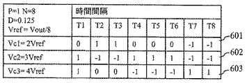
図1のn=3ビットの場合、[Vc1:Vc2:Vc3]=[1:2:4]Vref=[1:2:4]Vout/8である。 In the case of n = 3 bits in FIG. 1, [Vc1: Vc2: Vc3] = [1: 2: 4] Vref = [1: 2: 4] Vout / 8.
各ブリッジBiのスイッチのスイッチングパターンは、ブリッジのコネクタにおいて、VciがコンデンサーCiの電圧である場合に+Vci、−Vci又は0に等しい電圧Vbiを提供するように定義される。
さらに、各ビットBiのスイッチングパターンは、主スイッチ周期T=1/fの2n個の等しい連続したサブ周期ΔTとして適時に定義される。[1:2:4]の増倍係数を提供する周期的パターンで作動するRLBCにはいくつかの欠点がある。
The switching pattern of each bridge Bi switch is defined to provide a voltage Vbi equal to + Vci, -Vci or 0 at the connector of the bridge when Vci is the voltage of the capacitor Ci.
Furthermore, the switching pattern of each bit Bi is defined in a timely manner as 2 n equal consecutive sub-periods ΔT with a main switch period T = 1 / f. RLBC operating in a periodic pattern that provides a [1: 2: 4] multiplication factor has several drawbacks.
こうした場合、「2n」個のあり得る離散的な比/デューティサイクルしか実現することができない。n=3ビットの場合、8つの異なる昇圧比しか可能でない。したがって、出力電圧の調節は実現することが困難になる。デューティサイクルを平滑に選択することができないため、出力電圧を、所与の入力電圧の範囲に対して極めて広い範囲で調節しなければならない。しかしながら、昇圧コンバーターの出力電圧の範囲は、例えばインバーター等の特定の応用について広くすることができない。 In such a case, only “2 n ” possible discrete ratio / duty cycles can be achieved. For n = 3 bits, only 8 different boost ratios are possible. Therefore, it becomes difficult to realize the adjustment of the output voltage. Since the duty cycle cannot be chosen smoothly, the output voltage must be adjusted over a very wide range for a given input voltage range. However, the output voltage range of the boost converter cannot be widened for a particular application, such as an inverter.
Vci電圧は、各離散的なデューティサイクルに対して確定的に定義される(Vci=2i-1*Vout/8)。これにより、定格が最大電圧レベルである構成要素を有するように電源回路を設計する柔軟性が残らない。高い定格電圧レベルである構成要素を選択することにより、回路のコストが増大する可能性があり、構成要素のスイッチング電力損失も増大する可能性がある。 The Vci voltage is deterministically defined for each discrete duty cycle (Vci = 2 i-1 * Vout / 8). This leaves no flexibility in designing the power supply circuit to have components that are rated at the maximum voltage level. Selecting a component with a high rated voltage level can increase the cost of the circuit and can also increase the switching power loss of the component.
各コンデンサーの充放電パターンは、所与のデューティサイクルに対して固定され、コンデンサー間で異なり、各ビットを通過するRMS電流レベルが高レベルになる場合がある。電流のRMSレベルが高いことにより、通常、コンデンサーの寿命が劣化する。 The charge / discharge pattern of each capacitor is fixed for a given duty cycle, varies between capacitors, and the RMS current level passing through each bit may be high. The high RMS level of the current usually degrades the lifetime of the capacitor.
本発明は、種々の昇圧比の数を増大させることを目的とする。 The present invention aims to increase the number of different boost ratios.
本発明は、複数のビット、たとえば3つのビットB1、B2及びB3からなるRLBCに対する新しいスイッチ制御パターンを提案し、該スイッチ制御パターンでは、選択された周期的パターンが少なくとも1つの第2の周期的パターン又は少なくとも1つの第3の周期的パターンである場合に、ビットの少なくとも1つのコンデンサーの電圧値は異なったものとすることができる。
たとえば、3つのビットからなるRLBCに関して、選択された周期的パターンが少なくとも1つの第2の周期的パターンである場合、[Vc1:Vc2:Vc3]を[2:3:4]Vrefに等しいものとすることができ、選択された周期的パターンが少なくとも1つの第3の周期的パターンである場合、[Vc1:Vc2:Vc3]を[1:2:4]Vrefに等しいものとすることができる。
The present invention proposes a new switch control pattern for a RLBC consisting of a plurality of bits, eg three bits B1, B2 and B3, in which the selected periodic pattern is at least one second periodic pattern. In the case of a pattern or at least one third periodic pattern, the voltage value of at least one capacitor of the bits can be different.
For example, for a three-bit RLBC, if the selected periodic pattern is at least one second periodic pattern, [Vc1: Vc2: Vc3] equals [2: 3: 4] Vref And [Vc1: Vc2: Vc3] may be equal to [1: 2: 4] Vref if the selected periodic pattern is at least one third periodic pattern. it can.
ここで、RLBC回路のスイッチングコマンド法則を定義する。基本的に、各ビット電圧Vb1. . .Vb3は以下の式によって時間の関数として表わされる。

ここで、Λ(t)は、時間間隔幅ΔTのステップ関数を表す。スイッチの制御コマンド法則に関して、Si1、Si2は自身の値を{0;1}にとることができ、電圧Vbijは、以下の法則に従って、j番目の時間間隔Tjにおいて{−Vci,0;Vci}の値をとる。
εi,j=1-Si1j-Si2j
Here, Λ (t) represents a step function of the time interval width ΔT. With regard to the switch control command law, Si1 and Si2 can take their values {0; 1}, and the voltage Vbij is {−Vci, 0; Vci} in the jth time interval Tj according to the following law. Takes the value of
ε i, j = 1-Si1 j -Si2 j
Si1j及びSi2jは、j番目の時間間隔TjにおいてスイッチSilj及びSi2がON状態すなわち導通状態であるときは1に等しく、j番目の時間間隔TjにおいてスイッチSilj及びSi2がOFF状態すなわち非導通状態であるときはゼロ値に等しい。 Si1 j and Si2 j are equal to 1 when the switches Silj and Si2 are in the ON state, that is, the conducting state at the jth time interval Tj, and the switches Silj and Si2 are in the OFF state, that is, the nonconducting state at the jth time interval Tj Is equal to zero.
さらにVbiが基準電圧数値の整数倍として定義されるとすると、以下の式が得られる。
Vbij=εij2i-1Vref
Further, if Vbi is defined as an integer multiple of the reference voltage value, the following equation is obtained.
Vbij =
ここで、導通モード(S4=1)においてRLBC回路の電圧平衡条件を適用した場合、以下の式が得られる。
![]()
![]()
ここで、不連続モード(S4=0)においてRLBC回路の電圧平衡条件を適用した場合、以下の式が得られる。
![]()
![]()
定常状態分析において、各コンデンサー充電の平衡を検証すべきであり、これを以下の式によって表すことができる。
上記条件が満たされると、以下の項を計算する場合に昇圧挙動を検証することができる。
ここでnはビットの数に等しい。 Where n is equal to the number of bits.
これにより、条件
![]()
![]()
![]()
![]()
![]()
![]()
ここで、以下の項Ωjを導入する。
![]()
![]()
(a)及び(b)から、以下の式を得ることができる。
Vrefを任意に設定することができるため、αが1に等しく、第1の周期的パターン及び少なくとも1つの第2の周期的パターンの場合はVc1=2Vref、Vc2=3Vref及びVc3=4Vref、少なくとも1つの第3の周期的パターンの場合はVc1=Vref、Vc2=2Vref及びVc3=4Vrefとするように決めることができることが留意されるべきである。したがって、スイッチング規則{εij}の組を見つけることで十分である。
Vrefをさらに以下のように表すことができることが留意されるべきである。
![]()
![]()
n個のビットを有するRLBCのスイッチングパターンに対する解を見つけることは、所与の整数対{N,P}及び所与の整数ベクトルKに対して、
(i)行列(ε)が
![]()
(ii)
![]()
ような、サイズ(N×n)であり要素が{−1;0;1}にある行列(ε)を見つけることにある。
Finding a solution for a RLBC switching pattern with n bits is for a given integer pair {N, P} and a given integer vector K:
(I) The matrix (ε) is
![]()
(Ii)
![]()
Is to find a matrix (ε) having a size (N × n) and elements of {−1; 0; 1}.
本発明の第1の周期的パターン及び少なくとも1つの第2の周期的パターンに対して、整数ベクトルKは[2 3 4]であり、図5〜図9に開示する各行列は条件(i)及び(ii)を検証する。 For the first periodic pattern and at least one second periodic pattern of the present invention, the integer vector K is [2 3 4], and each matrix disclosed in FIGS. And (ii) is verified.
本発明の少なくとも1つの第3の周期的パターンに対して、整数ベクトルKは[1 2 4]であり、図10に開示する各行列は条件(i)及び(ii)を検証する。 For at least one third periodic pattern of the present invention, the integer vector K is [1 2 4] and each matrix disclosed in FIG. 10 verifies the conditions (i) and (ii).
図1bは、3つのブリッジ装置からなる昇圧コンバーターの第2の例である。 FIG. 1b is a second example of a boost converter consisting of three bridge devices.
図1aに関して開示したように、従来のDC/DC昇圧コンバーターのインダクターは、直列に接続された3に等しい「n」個のブリッジ装置に置き換えられる。各ブリッジ装置は、図1に示すように4つのスイッチ及び1つのコンデンサーからなる。この個々のブリッジ構造もまた「ビット」と呼ぶ。 As disclosed with respect to FIG. 1a, the inductor of a conventional DC / DC boost converter is replaced by “n” bridge devices equal to 3 connected in series. Each bridge device consists of four switches and one capacitor as shown in FIG. This individual bridge structure is also referred to as a “bit”.
図1bでは、3つのビットB1、B2及びB3を示す。 In FIG. 1b, three bits B1, B2 and B3 are shown.
ビットB1は、2つのダイオードD11及びD12、2つのスイッチS11及びS12並びに1つのコンデンサーC1からなる。 Bit B1 consists of two diodes D11 and D12, two switches S11 and S12 and one capacitor C1.
ビットB2は、2つのダイオードD21及びD22、2つのスイッチS21及びS22並びに1つのコンデンサーC2からなる。 Bit B2 consists of two diodes D21 and D22, two switches S21 and S22 and one capacitor C2.
ビットB3は、2つのダイオードD31及びD32’、2つのスイッチS31及びS32’並びに1つのコンデンサーC3からなる。 Bit B3 comprises two diodes D31 and D32 ', two switches S31 and S32', and one capacitor C3.
各ビットBi(i=1又は2)に対して、ダイオードDi1のアノードは、スイッチSi1の第1の端子に連結されている。Di1のカソードは、スイッチSi2の第1の端子及びコンデンサーCiの正の端子に連結されている。スイッチSi1の第2の端子は、コンデンサーCiの負の端子及びダイオードDi2のアノードに連結されている。ダイオードDi2のカソードは、スイッチSi2の第2の端子に連結されている。 For each bit Bi (i = 1 or 2), the anode of the diode Di1 is connected to the first terminal of the switch Si1. The cathode of Di1 is connected to the first terminal of switch Si2 and the positive terminal of capacitor Ci. The second terminal of the switch Si1 is connected to the negative terminal of the capacitor Ci and the anode of the diode Di2. The cathode of the diode Di2 is connected to the second terminal of the switch Si2.
ダイオードD31のアノードはスイッチS31の第1の端子に連結されている。D31のカソードはコンデンサーC3の正の端子及びダイオードD32’のアノードに連結されている。スイッチS31の第2の端子は、コンデンサーC3の負の端子及びスイッチS32’の第1の端子に連結されている。 The anode of the diode D31 is connected to the first terminal of the switch S31. The cathode of D31 is connected to the positive terminal of capacitor C3 and the anode of diode D32 '. The second terminal of the switch S31 is connected to the negative terminal of the capacitor C3 and the first terminal of the switch S32 '.
光起電素子PVのような直流電気提供手段が、入力電圧Vinを提供する。直流電気提供手段の正の端子は、ダイオードD11のアノードに接続されている。 DC electricity providing means, such as the photovoltaic element PV, provides the input voltage Vin. The positive terminal of the DC electricity providing means is connected to the anode of the diode D11.
ダイオードD12のカソードはダイオードD21のアノードに接続されている。 The cathode of the diode D12 is connected to the anode of the diode D21.
ダイオードD22のカソードはダイオードD31のアノードに接続されている。 The cathode of the diode D22 is connected to the anode of the diode D31.
ダイオードD32’のカソードはコンデンサーCLの正の端子に接続されている。 The cathode of the diode D32 'is connected to the positive terminal of the capacitor CL.
コンデンサーCLの負の端子及びスイッチS32’の第2の端子は、直流電気提供手段の負の端子に接続されている。 The negative terminal of the capacitor CL and the second terminal of the switch S32 'are connected to the negative terminal of the DC electricity providing means.
スイッチS32’は図1aのスイッチS4と同様に作用し、ダイオードD32’は図1aのダイオードD4のように作用する。 Switch S32 'operates similarly to switch S4 in FIG. 1a, and diode D32' operates like diode D4 in FIG. 1a.
コンデンサーCLにおける電圧はVoutに等しい。 The voltage at the capacitor CL is equal to Vout.
B1の入力と出力との間の電圧の差をVb1と呼び、B2の入力と出力との電圧の差をVb2と呼び、B3の入力と出力との電圧の差をVb3と呼ぶ。Vb3は、スイッチS32’がON状態であるときにVb3*に等しく、スイッチS32’がOFF状態であるときにVb3**に等しい。 The voltage difference between the input and output of B1 is called Vb1, the voltage difference between the input and output of B2 is called Vb2, and the voltage difference between the input and output of B3 is called Vb3. Vb3 is equal to Vb3 * when the switch S32 ′ is in the ON state, and is equal to Vb3 ** when the switch S32 ′ is in the OFF state.
図2は、複数のブリッジ装置からなる昇圧コンバーターを備えた装置の一例を表す。 FIG. 2 shows an example of a device including a boost converter composed of a plurality of bridge devices.
装置20は、たとえば、バス201によって互いに接続された構成要素と、図11に開示するようなアルゴリズムに関連するプログラムによって制御されるプロセッサー200とに基づくアーキテクチャを有している。
The
ここで、装置20は、変形形態では、以下に開示するようにプロセッサー200によって実行されるものと同じ動作を実行する1つ又はいくつかの専用集積回路の形態で実装されることが留意されなければならない。
It has to be noted here that the
バス201は、プロセッサー200を、リードオンリーメモリROM202、ランダムアクセスメモリRAM203、アナログ/デジタル変換器ADC206及び図1に開示するもののようなRLBCモジュールに連結する。
The
リードオンリーメモリROM202は、図11に開示するようなアルゴリズムに関連するプログラムの命令を含み、それらは、装置20に電源が投入された際にランダムアクセスメモリRAM203に転送される。
The read-
リードオンリーメモリROM202は、本発明の図3〜図10に示す表を記憶する。
The read only
RAMメモリー203は、変数を受け取るように意図されたレジスターと、図11に開示するようなアルゴリズムに関連するプログラムの命令とを含む。
アナログ/デジタル変換器206は、RLBCに接続され、入力電圧Vin及び/又は出力電圧Voutを表す電圧を2値情報に変換する。
The analog /
図3aは、k1が2に等しく、k2が3に等しく、k3が4に等しい場合の、本発明による第1の周期的パターン及び少なくとも1つの第2の周期的パターンによって提供することができる種々の昇圧比を表す表を表す。 FIG. 3a is provided by a first periodic pattern and at least one second periodic pattern according to the invention when k 1 is equal to 2, k 2 is equal to 3 and k 3 is equal to 4. 1 represents a table representing various boost ratios that can be
図3aの表は、300〜306で示す6つの列を含む。
列300は、RLBCに印加される入力電圧Vinの種々の値を示す。
列301は、RLBCの出力電圧Voutを示す。たとえば、出力電圧は240ボルトに等しい。
列302は、出力電圧Voutと入力電圧Vinとの間の種々の比を示す。
列303は、RLBCの種々のデューティサイクルDを示す。
列304は、対N及びPの種々の値を示す。
列305は、基準電圧Vrefの種々の値を示す。
列306は、入力電圧値Vinに従って選択される図を示す。
The table of FIG. 3a includes six columns, indicated as 300-306.
行310において、入力電圧は24ボルトに等しく、出力電圧は240ボルトであり、比Vout/Vinは10に等しく、デューティサイクルDは0.9に等しく、対(N,P)は(10,9)に等しく、基準電圧Vrefは24ボルトに等しく、10の比を得るために選択すべきスイッチングパターンは図5aに開示されている。
In
行311において、入力電圧は30ボルトに等しく、出力電圧は240ボルトであり、比Vout/Vinは8に等しく、デューティサイクルDは0.875に等しく、対(N,P)は(8,7)に等しく、基準電圧Vrefは30ボルトに等しく、8の比を得るために選択すべきスイッチングパターンは図6dに開示されている。
In
行312において、入力電圧は34.3ボルトに等しく、出力電圧は240ボルトであり、比Vout/Vinは7に等しく、デューティサイクルDは0.857に等しく、対(N,P)は(7,6)に等しく、基準電圧Vrefは34.3ボルトに等しく、7の比を得るために選択すべきスイッチングパターンは図7bに開示されている。
In
行313において、入力電圧は40ボルトに等しく、出力電圧は240ボルトであり、比Vout/Vinは6に等しく、デューティサイクルDは0.833に等しく、対(N,P)は(6,5)に等しく、基準電圧Vrefは40ボルトに等しく、6の比を得るために選択すべきスイッチングパターンは図8aに開示されている。
In
行314において、入力電圧は48ボルトに等しく、出力電圧は240ボルトであり、比Vout/Vinは5に等しく、デューティサイクルDは0.8に等しく、対(N,P)は(5,4)に等しく、基準電圧Vrefは48ボルトに等しく、5の比を得るために選択すべきスイッチングパターンは図9aに開示されている。
In
行315において、入力電圧は90ボルトに等しく、出力電圧は240ボルトであり、比Vout/Vinは2.67に等しく、デューティサイクルDは0.625に等しく、対(N,P)は(8,5)に等しく、基準電圧Vrefは30ボルトに等しく、2.67の比を得るために選択すべきスイッチングパターンは図6bに開示されている。 In row 315, the input voltage is equal to 90 volts, the output voltage is 240 volts, the ratio Vout / Vin is equal to 2.67, the duty cycle D is equal to 0.625, and the pair (N, P) is (8 5), the reference voltage V ref is equal to 30 volts, and the switching pattern to be selected to obtain a ratio of 2.67 is disclosed in FIG. 6b.
行316において、入力電圧は96ボルトに等しく、出力電圧は240ボルトであり、比Vout/Vinは2.5に等しく、デューティサイクルDは0.6に等しく、対(N,P)は(5,3)に等しく、基準電圧Vrefは48ボルトに等しく、2.5の比を得るために選択すべきスイッチングパターンは図9bに開示されている。
In
行317において、入力電圧は144ボルトに等しく、出力電圧は240ボルトであり、比Vout/Vinは1.67に等しく、デューティサイクルDは0.4に等しく、対(N,P)は(5,2)に等しく、基準電圧Vrefは48ボルトに等しく、1.67の比を得るために選択すべきスイッチングパターンは図9cに開示されている。
In
行318において、入力電圧は150ボルトに等しく、出力電圧は240ボルトであり、比Vout/Vinは1.6に等しく、デューティサイクルDは0.375に等しく、対(N,P)は(8,3)に等しく、基準電圧Vrefは30ボルトに等しく、1.6の比を得るために選択すべきスイッチングパターンは図6cに開示されている。
In
行319において、入力電圧は192ボルトに等しく、出力電圧は240ボルトであり、比Vout/Vinは1.25に等しく、デューティサイクルDは0.2に等しく、対(N,P)は(5,1)に等しく、基準電圧Vrefは48ボルトに等しく、1.25の比を得るために選択すべきスイッチングパターンは図9dに開示されている。
In
行320において、入力電圧は200ボルトに等しく、出力電圧は240ボルトであり、比Vout/Vinは1.2に等しく、デューティサイクルDは0.166に等しく、対(N,P)は(6,1)に等しく、基準電圧Vrefは40ボルトに等しく、1.2の比を得るために選択すべきスイッチングパターンは図8bに開示されている。
In
行321において、入力電圧は205.7ボルトに等しく、出力電圧は240ボルトであり、比Vout/Vinは1.16に等しく、デューティサイクルDは0.142に等しく、対(N,P)は(7,1)に等しく、基準電圧Vrefは34.3ボルトに等しく、1.16の比を得るために選択すべきスイッチングパターンは図7aに開示されている。
In
行322において、入力電圧は210ボルトに等しく、出力電圧は240ボルトであり、比Vout/Vinは1.14に等しく、デューティサイクルDは0.125に等しく、対(N,P)は(8,1)に等しく、基準電圧Vrefは30ボルトに等しく、1.14の比を得るために選択すべきスイッチングパターンは図6aに開示されている。
In
行323において、入力電圧は216ボルトに等しく、出力電圧は240ボルトであり、比Vout/Vinは1.11に等しく、デューティサイクルDは0.1に等しく、対(N,P)は(10,1)に等しく、基準電圧Vrefは24ボルトに等しく、1.1の比を得るために選択すべきスイッチングパターンは図5bに開示されている。
In
図3bは、p1が1に等しく、p2が2に等しく、p3が4に等しい場合の、本発明による少なくとも1つの第3の周期的パターンによって提供することができる種々の昇圧比を表す表を表す。 FIG. 3b shows various boost ratios that can be provided by at least one third periodic pattern according to the invention when p 1 is equal to 1, p 2 is equal to 2 and p 3 is equal to 4. Represents the table to represent.
図3bの表は、350〜356で示す6つの列を含む。
列350は、RLBCに印加される入力電圧Vinの種々の値を示す。
列351は、RLBCの出力電圧Voutを示す。たとえば、出力電圧は240ボルトに等しい。
列352は、出力電圧Voutと入力電圧Vinとの間の種々の比を示す。
列353は、RLBCの種々のデューティサイクルDを示す。
列354は、対N及びPの種々の値を示す。
列355は、基準電圧Vrefの種々の値を示す。
列356は、入力電圧値Vinに従って選択される図を示す。
The table of FIG. 3b includes six columns denoted 350-356.
行361において、入力電圧は60ボルトに等しく、出力電圧は240ボルトであり、比Vout/Vinは4に等しく、デューティサイクルDは0.75に等しく、対(N,P)は(8,6)に等しく、基準電圧Vrefは30ボルトに等しく、4の比を得るために選択すべきスイッチングパターンは図10aに開示されている。
In
行362において、入力電圧は48ボルトに等しく、出力電圧は240ボルトであり、比Vout/Vinは5に等しく、デューティサイクルDは0.8に等しく、対(N,P)は(5,4)に等しく、基準電圧Vrefは30ボルトに等しく、5の比を得るために選択すべきスイッチングパターンは図10bに開示されている。
In
図4aは、3つのブリッジ装置からなる昇圧コンバーターのブリッジにおいて種々の電圧を得るために、図1aに示す昇圧コンバーターの第1の例のスイッチのスイッチング状態を表す表を表す。 FIG. 4a represents a table representing the switching states of the switches of the first example of the boost converter shown in FIG. 1a in order to obtain different voltages in the bridge of the boost converter consisting of three bridge devices.
列400〜402はビットB1に関連し、列403〜405はビットB2に関連し、列406〜408はビットB3に関連する。 Columns 400-402 are associated with bit B1, columns 403-405 are associated with bit B2, and columns 406-408 are associated with bit B3.
行411は、
Vc1に等しい電圧Vb1の場合、スイッチS11は非導通状態にあり、スイッチS12は非導通状態にあり、
Vc2に等しい電圧Vb2の場合、スイッチS21は非導通状態にあり、スイッチS22は非導通状態にあり、
Vc3に等しい電圧Vb3の場合、スイッチS31は非導通状態にあり、スイッチS32は非導通状態にあることを示す。
For a voltage Vb1 equal to Vc1, switch S11 is non-conductive, switch S12 is non-conductive,
For a voltage Vb2 equal to Vc2, switch S21 is non-conductive, switch S22 is non-conductive,
When the voltage Vb3 is equal to Vc3, the switch S31 is in a non-conductive state, and the switch S32 is in a non-conductive state.
行412は、
ゼロ値に等しい電圧Vb1の場合、スイッチS11は非導通状態にあり、スイッチS12は導通状態にあり、
ゼロ値に等しい電圧Vb2の場合、スイッチS21は非導通状態にあり、スイッチS22は導通状態にあり、
ゼロ値に等しい電圧Vb3の場合、スイッチS32が非導通状態にあるときにスイッチS31が導通状態にあるか、又はスイッチS32が導通状態にあるときにスイッチS31が非導通状態にあることを示す。
For voltage Vb1 equal to zero value, switch S11 is non-conductive, switch S12 is conductive,
For voltage Vb2 equal to zero value, switch S21 is non-conductive, switch S22 is conductive,
A voltage Vb3 equal to a zero value indicates that the switch S31 is in a conductive state when the switch S32 is in a non-conductive state, or the switch S31 is in a non-conductive state when the switch S32 is in a conductive state.
行413は、
−Vc1に等しい電圧Vb1の場合、スイッチS11は導通状態にあり、スイッチS12は導通状態にあり、
−Vc2に等しい電圧Vb2の場合、スイッチS21は導通状態にあり、スイッチS22は導通状態にあり、
−Vc3に等しい電圧Vb3の場合、スイッチS31は導通状態にあり、スイッチS32は導通状態にあることを示す。
For a voltage Vb1 equal to −Vc1, the switch S11 is in a conducting state, the switch S12 is in a conducting state,
For a voltage Vb2 equal to −Vc2, the switch S21 is in a conducting state, the switch S22 is in a conducting state,
In the case of the voltage Vb3 equal to −Vc3, the switch S31 is in a conductive state, and the switch S32 is in a conductive state.
図4bは、3つのブリッジ装置からなる昇圧コンバーターのブリッジにおいて種々の電圧を得るために、図1bに示す昇圧コンバーターの第2の例のスイッチのスイッチング状態を表す表を表す。 FIG. 4b represents a table representing the switching states of the switches of the second example of the boost converter shown in FIG. 1b in order to obtain various voltages in the bridge of the boost converter consisting of three bridge devices.
列420〜422はビットB1に関連し、列423〜425はビットB2に関連し、列426〜428はビットB3に関連する。 Columns 420-422 are associated with bit B1, columns 423-425 are associated with bit B2, and columns 426-428 are associated with bit B3.
行431は、
Vc1に等しい電圧Vb1の場合、スイッチS11は非導通状態にあり、スイッチS12は非導通状態にあり、
Vc2に等しい電圧Vb2の場合、スイッチS21は非導通状態にあり、スイッチS22は非導通状態にあり、
Vc3に等しい電圧Vb3の場合、スイッチS31は非導通状態にあり、スイッチS32’は導通状態にあることを示す。
For a voltage Vb1 equal to Vc1, switch S11 is non-conductive, switch S12 is non-conductive,
For a voltage Vb2 equal to Vc2, switch S21 is non-conductive, switch S22 is non-conductive,
When the voltage Vb3 is equal to Vc3, the switch S31 is in a non-conducting state and the switch S32 ′ is in a conducting state.
行432は、
ゼロ値に等しい電圧Vb1の場合、スイッチS11は非導通状態にあり、スイッチS12は導通状態にあり、
ゼロ値に等しい電圧Vb2の場合、スイッチS21は非導通状態にあり、スイッチS22は導通状態にあり、
ゼロ値に等しい電圧Vb3の場合、スイッチS31及びS32’は共に導通状態又は非導通状態にあることを示す。
For voltage Vb1 equal to zero value, switch S11 is non-conductive, switch S12 is conductive,
For voltage Vb2 equal to zero value, switch S21 is non-conductive, switch S22 is conductive,
In the case of the voltage Vb3 equal to the zero value, it indicates that both the switches S31 and S32 ′ are in a conductive state or a non-conductive state.
行433は、
−Vc1に等しい電圧Vb1の場合、スイッチS11は導通状態にあり、スイッチS12は導通状態にあり、
−Vc2に等しい電圧Vb2の場合、スイッチS21は導通状態にあり、スイッチS22は導通状態にあり、
−Vc3に等しい電圧Vb3の場合、スイッチS31は導通状態にあり、スイッチS32’は非導通状態にあることを示す。
For a voltage Vb1 equal to −Vc1, the switch S11 is in a conducting state, the switch S12 is in a conducting state,
For a voltage Vb2 equal to −Vc2, the switch S21 is in a conducting state, the switch S22 is in a conducting state,
For voltage Vb3 equal to −Vc3, switch S31 is in a conducting state and switch S32 ′ is in a non-conducting state.
本発明の実現形態の一例によれば、
選択された周期的パターンが少なくとも1つの第2の周期的パターンの場合、Vc1=2Vref、Vc2=3Vref及びVc3=4Vrefであり、
選択された周期的パターンが少なくとも1つの第3の周期的パターンである場合、Vc1=Vref、Vc2=2Vref及びVc3=4Vrefである。
According to an example of implementation of the present invention,
If the selected periodic pattern is at least one second periodic pattern, Vc1 = 2V ref , Vc2 = 3V ref and Vc3 = 4V ref ,
If the selected periodic pattern is at least one third periodic pattern, Vc1 = V ref , Vc2 = 2V ref and Vc3 = 4V ref .
図5a及び5bは、第1の周期的パターン又は少なくとも1つの第2の周期的パターンが10個の時間間隔に分解される場合に種々の昇圧比を有するための、昇圧コンバーターのブリッジにおける電圧値の例である。 FIGS. 5a and 5b show the voltage values at the bridge of the boost converter for having different boost ratios when the first periodic pattern or at least one second periodic pattern is resolved into 10 time intervals. It is an example.
行501及び511において、1に等しい値はVb1=2Vrefを意味し、−1に等しい値はVb1=−2Vrefを意味し、0に等しい値はVb1=0を意味する。
In
行501及び511において、1に等しい値はVb2=3Vrefを意味し、−1に等しい値はVb2=−3Vrefを意味し、0に等しい値はVb2=0を意味する。
In
行501及び511において、1に等しい値はVb3=4Vrefを意味し、−1に等しい値はVb3=−4Vrefを意味し、0に等しい値はVb3=0を意味する。
In
各時間間隔T1〜T10の持続時間はΔT=T/N(N=10)であり、ここで、Tは、図1aのスイッチS4によるか又は図1bのスイッチS32’によって作動するサイクルの持続時間である。 The duration of each time interval T1-T10 is ΔT = T / N (N = 10), where T is the duration of the cycle operated by switch S4 in FIG. 1a or by switch S32 ′ in FIG. 1b. It is.
図5aは、比Vout/Vin=N/(N−P)=10(D=0.9)を有するためのRLBCのブリッジにおける電圧値を含む。 FIG. 5a includes the voltage values at the RLBC bridge to have the ratio Vout / Vin = N / (N−P) = 10 (D = 0.9).
比Vout/Vin=10を得るために、10個の時間間隔が必要である。 Ten time intervals are required to obtain the ratio Vout / Vin = 10.
時間間隔T1及びT2では、Vb1=−2Vref、Vb2=3Vref及びVb3=0である。
時間間隔T3、T4、T5及びT6では、Vb1=0、Vb2=−3Vref及びVb3=4Vrefである。
時間間隔T7、T8及びT9では、Vb1=2Vref、Vb2=3Vref及びVb3=−4Vrefである。
時間間隔T10では、Vb1=−2Vref、Vb2=−3Vref及びVb3=−4Vrefである。
In the time intervals T1 and T2, Vb1 = −2V ref , Vb2 = 3V ref and Vb3 = 0.
In the time intervals T3, T4, T5 and T6, Vb1 = 0, Vb2 = -3V ref and Vb3 = 4V ref .
In the time intervals T7, T8 and T9, Vb1 = 2V ref , Vb2 = 3V ref and Vb3 = −4V ref .
In the time interval T10, Vb1 = -2V ref , Vb2 = -3V ref and Vb3 = -4V ref .
これらの電圧値が図1aの昇圧コンバーターのブリッジの電圧値である場合、スイッチS4は、時間間隔T1〜T9(P=9)の間は導通状態であり、時間間隔T10(N=10)では非導通状態である。 When these voltage values are the voltage values of the bridge of the boost converter of FIG. 1a, the switch S4 is conductive during the time intervals T1 to T9 (P = 9) and in the time interval T10 (N = 10). Non-conducting state.
図5bは、比Vout/Vin=N/(N−P)=1.11(D=0.1)を有するためのRLBCのブリッジにおける電圧値を含む。 FIG. 5b includes the voltage values at the RLBC bridge to have the ratio Vout / Vin = N / (N−P) = 1.11 (D = 0.1).
比Vout/Vin=1.11を得るために、10個の時間間隔が必要である。 Ten time intervals are required to obtain the ratio Vout / Vin = 1.11.
時間間隔T1では、Vb1=2Vref、Vb2=3Vref及びVb3=4Vrefである。
時間間隔T2及びT3では、Vb1=2Vref、Vb2=−3Vref及びVb3=0である。
時間間隔T4、T5、T6及びT7では、Vb1=0、Vb2=3Vref及びVb3=−4Vrefである。
時間間隔T8、T9及びT10では、Vb1=−2Vref、Vb2=−3Vref及びVb3=4Vrefである。
In the time interval T1, Vb1 = 2V ref , Vb2 = 3V ref and Vb3 = 4V ref .
In the time intervals T2 and T3, Vb1 = 2V ref , Vb2 = −3V ref and Vb3 = 0.
At time intervals T4, T5, T6 and T7, Vb1 = 0, Vb2 = 3V ref and Vb3 = -4V ref .
In the time intervals T8, T9 and T10, Vb1 = −2V ref , Vb2 = −3V ref and Vb3 = 4V ref .
これらの電圧値が図1aの昇圧コンバーターのブリッジの電圧値である場合、スイッチS4は、時間間隔T1(P=1)の間は導通状態であり、時間間隔T2〜T10(N=10)では非導通状態である。 If these voltage values are the voltage values of the bridge of the boost converter of FIG. 1a, the switch S4 is conductive during the time interval T1 (P = 1) and in the time intervals T2 to T10 (N = 10). Non-conducting state.
図6a〜6dは、第1の周期的パターン又は少なくとも1つの第2の周期的パターンが8つの時間間隔に分解される場合に種々の昇圧比を有するための、3つのブリッジ装置からなる昇圧コンバーターのブリッジにおける電圧値の例である。 FIGS. 6a-6d show a boost converter consisting of three bridge devices for having different boost ratios when the first periodic pattern or at least one second periodic pattern is resolved into eight time intervals. It is an example of the voltage value in a bridge | bridging.
行601、611、621及び631において、1に等しい値はVb1=2Vrefを意味し、−1に等しい値はVb1=−2Vrefを意味し、0に等しい値はVb1=0を意味する。
In
行602、612、622及び632において、1に等しい値はVb2=3Vrefを意味し、−1に等しい値はVb2=−3Vrefを意味し、0に等しい値はVb2=0を意味する。
In
行603、613、623及び633において、1に等しい値はVb3=4Vrefを意味し、−1に等しい値はVb3=−4Vrefを意味し、0に等しい値はVb3=0を意味する。
In
各時間間隔T1〜T8の持続時間はΔT=T/N(N=8)であり、ここで、Tは、図1aのスイッチS4によるか又は図1bのスイッチS32’によって作動するサイクルの持続時間である。 The duration of each time interval T1-T8 is ΔT = T / N (N = 8), where T is the duration of the cycle operated by switch S4 in FIG. 1a or by switch S32 ′ in FIG. 1b. It is.
図6aは、比Vout/Vin=N/(N−P)=1.14(D=0.125)を有するためのRLBCのブリッジにおける電圧値を含む。 FIG. 6a includes the voltage values at the RLBC bridge to have the ratio Vout / Vin = N / (N−P) = 1.14 (D = 0.125).
比Vout/Vin=1.14を得るために、8つの時間間隔が必要である。 To obtain the ratio Vout / Vin = 1.14, 8 time intervals are required.
時間間隔T1では、Vb1=0、Vb2=3Vref及びVb3=4Vrefである。
時間間隔T2及びT3では、Vb1=2Vref、Vb2=−3Vref及びVb3=0である。
時間間隔T4、T5及びT6では、Vb1=0、Vb2=3Vref及びVb3=−4Vrefである。
時間間隔T7及びT8では、Vb1=−2Vref、Vb2=−3Vref及びVb3=4Vrefである。
In the time interval T1, Vb1 = 0, Vb2 = 3V ref and Vb3 = 4V ref .
In the time intervals T2 and T3, Vb1 = 2V ref , Vb2 = −3V ref and Vb3 = 0.
At time intervals T4, T5 and T6, Vb1 = 0, Vb2 = 3V ref and Vb3 = -4V ref .
At time intervals T7 and T8, Vb1 = -2V ref , Vb2 = -3V ref and Vb3 = 4V ref .
これらの電圧値が図1aの昇圧コンバーターのブリッジの電圧値である場合、スイッチS4は、時間間隔T1(P=1)の間は導通状態であり、時間間隔T2〜T8(N=8)では非導通状態である。 If these voltage values are the voltage values of the bridge of the boost converter of FIG. 1a, the switch S4 is conductive during the time interval T1 (P = 1) and in the time intervals T2 to T8 (N = 8). Non-conducting state.
図6bは、比Vout/Vin=N/(N−P)=2.67(D=0.625)を有するためのRLBCのブリッジにおける電圧値を含む。 FIG. 6b includes the voltage values at the RLBC bridge to have the ratio Vout / Vin = N / (N−P) = 2.67 (D = 0.625).
比Vout/Vin=2.67を得るために、8つの時間間隔が必要である。 To obtain the ratio Vout / Vin = 2.67, 8 time intervals are required.
時間間隔T1では、Vb1=2Vref、Vb2=−3Vref及びVb3=4Vrefである。
時間間隔T2、T3、T4及びT5では、Vb1=0、Vb2=3Vref及びVb3=0である。
時間間隔T6及びT7では、Vb1=−2Vref、Vb2=−3Vref及びVb3=0である。
時間間隔T8では、Vb1=2Vref、Vb2=−3Vref及びVb3=−4Vrefである。
In the time interval T1, Vb1 = 2V ref , Vb2 = −3V ref and Vb3 = 4V ref .
In time interval T2, T3, T4 and T5, it is Vb1 = 0, Vb2 = 3V ref and Vb3 = 0.
In the time intervals T6 and T7, Vb1 = −2V ref , Vb2 = −3V ref and Vb3 = 0.
In the time interval T8, Vb1 = 2V ref , Vb2 = −3V ref and Vb3 = −4V ref .
これらの電圧値が図1aの昇圧コンバーターのブリッジの電圧値である場合、スイッチS4は、時間間隔T1〜T5(P=5)の間は導通状態であり、時間間隔T6〜T8(N=8)では非導通状態である。 If these voltage values are the voltage values of the bridge of the boost converter of FIG. 1a, the switch S4 is conductive during the time intervals T1 to T5 (P = 5) and the time intervals T6 to T8 (N = 8). ) Is a non-conductive state.
図6cは、比Vout/Vin=N/(N−P)=1.6(D=0.375)を有するためのRLBCのブリッジにおける電圧値を含む。 FIG. 6c includes the voltage values at the RLBC bridge to have the ratio Vout / Vin = N / (N−P) = 1.6 (D = 0.375).
比Vout/Vin=1.6を得るために、8つの時間間隔が必要である。 Eight time intervals are required to obtain the ratio Vout / Vin = 1.6.
時間間隔T1では、Vb1=−2Vref、Vb2=3Vref及びVb3=4Vrefである。
時間間隔T2及びT3では、Vb1=2Vref、Vb2=3Vref及びVb3=0である。
時間間隔T4では、Vb1=−2Vref、Vb2=3Vref及びVb3=−4Vrefである。
時間間隔T5、T6、T7及びT8では、Vb1=0、Vb2=−3Vref及びVb3=0である。
In the time interval T1, Vb1 = −2V ref , Vb2 = 3V ref and Vb3 = 4V ref .
In time intervals T2 and T3, Vb1 = 2V ref , Vb2 = 3V ref and Vb3 = 0.
In the time interval T4, Vb1 = −2V ref , Vb2 = 3V ref and Vb3 = −4V ref .
In the time intervals T5, T6, T7 and T8, Vb1 = 0, Vb2 = -3V ref and Vb3 = 0.
これらの電圧値が図1aの昇圧コンバーターのブリッジの電圧値である場合、スイッチS4は、時間間隔T1〜T3(P=3)の間は導通状態であり、時間間隔T4〜T8(N=8)では非導通状態である。 If these voltage values are the voltage values of the bridge of the boost converter of FIG. 1a, the switch S4 is conductive during the time intervals T1 to T3 (P = 3) and the time intervals T4 to T8 (N = 8). ) Is a non-conductive state.
図6dは、比Vout/Vin=N/(N−P)=8(D=0.875)を有するためのRLBCのブリッジにおける電圧値を含む。 FIG. 6d includes the voltage values at the bridge of RLBC to have the ratio Vout / Vin = N / (N−P) = 8 (D = 0.875).
比Vout/Vin=8を得るために、8つの時間間隔が必要である。 To obtain the ratio Vout / Vin = 8, 8 time intervals are required.
時間間隔T1及びT2では、Vb1=−2Vref、Vb2=3Vref及びVb3=0である。
時間間隔T3、T4及びT5では、Vb1=0、Vb2=−3Vref及びVb3=4Vrefである。
時間間隔T6及びT7では、Vb1=2Vref、Vb2=3Vref及びVb3=−4Vrefである。
時間間隔T8では、Vb1=0、Vb2=−3Vref及びVb3=−4Vrefである。
In the time intervals T1 and T2, Vb1 = −2V ref , Vb2 = 3V ref and Vb3 = 0.
In the time intervals T3, T4 and T5, Vb1 = 0, Vb2 = -3V ref and Vb3 = 4V ref .
At time intervals T6 and T7, Vb1 = 2V ref , Vb2 = 3V ref and Vb3 = −4V ref .
At time interval T8, Vb1 = 0, Vb2 = -3V ref and Vb3 = -4V ref .
これらの電圧値が図1aの昇圧コンバーターのブリッジの電圧値である場合、スイッチS4は、時間間隔T1〜T1(P=7)の間は導通状態であり、時間間隔T2〜T8(N=8)では非導通状態である。 If these voltage values are the voltage values of the bridge of the boost converter of FIG. 1a, the switch S4 is conductive during the time intervals T1 to T1 (P = 7) and the time intervals T2 to T8 (N = 8). ) Is a non-conductive state.
図7a及び図7bは、第1の周期的パターン又は少なくとも1つの第2の周期的パターンが7つの時間間隔に分解される場合に種々の昇圧比を有するための、3つのブリッジ装置からなる昇圧コンバーターのブリッジにおける電圧値の例である。 7a and 7b show a boost consisting of three bridge devices for having different boost ratios when the first periodic pattern or at least one second periodic pattern is resolved into seven time intervals. It is an example of the voltage value in the bridge | bridging of a converter.
行701及び711において、1に等しい値はVb1=2Vrefを意味し、−1に等しい値はVb1=−2Vrefを意味し、0に等しい値はVb1=0を意味する。
In
行702及び712において、1に等しい値はVb2=3Vrefを意味し、−1に等しい値はVb2=−3Vrefを意味し、0に等しい値はVb2=0を意味する。
In
行703及び713において、1に等しい値はVb3=4Vrefを意味し、−1に等しい値はVb3=−4Vrefを意味し、0に等しい値はVb3=0を意味する。
In
各時間間隔T1〜T7の持続時間はΔT=T/N(N=7)であり、ここで、Tは、図1aのスイッチS4によるか又は図1bのスイッチS32’によって作動するサイクルの持続時間である。 The duration of each time interval T1-T7 is ΔT = T / N (N = 7), where T is the duration of the cycle operated by switch S4 in FIG. 1a or by switch S32 ′ in FIG. 1b. It is.
図7aは、比Vout/Vin=N/(N−P)=1.16(D=0.142)を有するためのRLBCのブリッジにおける電圧値を含む。 FIG. 7a includes the voltage values at the RLBC bridge to have the ratio Vout / Vin = N / (N−P) = 1.16 (D = 0.142).
比Vout/Vin=1.16を得るために、7つの時間間隔が必要である。 In order to obtain the ratio Vout / Vin = 1.16, seven time intervals are required.
時間間隔T1では、Vb1=2Vref、Vb2=0及びVb3=4Vrefである。
時間間隔T2、T3、及びT4では、Vb1=0、Vb2=3Vref及びVb3=−4Vrefである。
時間間隔T5では、Vb1=2Vref、Vb2=−3Vref及びVb3=0である。
時間間隔T6及びT7では、Vb1=−2Vref、Vb2=−3Vref及びVb3=4Vrefである。
In the time interval T1, Vb1 = 2V ref , Vb2 = 0 and Vb3 = 4V ref .
At time intervals T2, T3, and T4, Vb1 = 0, Vb2 = 3V ref, and Vb3 = -4V ref .
In the time interval T5, Vb1 = 2V ref , Vb2 = -3V ref and Vb3 = 0.
In the time intervals T6 and T7, Vb1 = −2V ref , Vb2 = −3V ref and Vb3 = 4V ref .
これらの電圧値が図1aの昇圧コンバーターのブリッジの電圧値である場合、スイッチS4は、時間間隔T1〜T6(P=1)の間は導通状態であり、時間間隔T7(N=7)では非導通状態である。 When these voltage values are the voltage values of the bridge of the boost converter of FIG. 1a, the switch S4 is conductive during the time intervals T1 to T6 (P = 1) and in the time interval T7 (N = 7). Non-conducting state.
図7bは、比Vout/Vin=N/(N−P)=7(D=0.857)を有するためのRLBCのブリッジにおける電圧値を含む。 FIG. 7b includes the voltage values at the RLBC bridge to have the ratio Vout / Vin = N / (N−P) = 7 (D = 0.857).
比Vout/Vin=7を得るために、7つの時間間隔が必要である。 In order to obtain the ratio Vout / Vin = 7, seven time intervals are required.
時間間隔T1及びT2では、Vb1=2Vref、Vb2=3Vref及びVb3=−4Vrefである。
時間間隔T3、T4及びT5では、Vb1=0、Vb2=−3Vref及びVb3=4Vrefである。
時間間隔T6では、Vb1=−2Vref、Vb2=3Vref及びVb3=0である。
時間間隔T7では、Vb1=−2Vref、Vb2=0及びVb3=−4Vrefである。
At time intervals T1 and T2, Vb1 = 2V ref , Vb2 = 3V ref and Vb3 = −4V ref .
In the time intervals T3, T4 and T5, Vb1 = 0, Vb2 = -3V ref and Vb3 = 4V ref .
At time interval T6, Vb1 = −2V ref , Vb2 = 3V ref and Vb3 = 0.
In the time interval T7, Vb1 = −2V ref , Vb2 = 0 and Vb3 = −4V ref .
これらの電圧値が図1aの昇圧コンバーターのブリッジの電圧値である場合、スイッチS4は、時間間隔T1(P=6)の間は導通状態であり、時間間隔T2〜T7(N=7)では非導通状態である。 If these voltage values are the voltage values of the bridge of the boost converter of FIG. 1a, the switch S4 is conductive during the time interval T1 (P = 6) and in the time intervals T2 to T7 (N = 7). Non-conducting state.
図8a及び8bは、第1の周期的パターン又は少なくとも1つの第2の周期的パターンが6つの時間間隔に分解される場合に種々の昇圧比を有するための、3つのブリッジ装置からなる昇圧コンバーターのブリッジにおける電圧値の例である。 FIGS. 8a and 8b show a boost converter consisting of three bridge devices for having different boost ratios when the first periodic pattern or at least one second periodic pattern is resolved into six time intervals. It is an example of the voltage value in a bridge | bridging.
行801及び811において、1に等しい値はVb1=2Vrefを意味し、−1に等しい値はVb1=−2Vrefを意味し、0に等しい値はVb1=0を意味する。
In
行802及び812において、1に等しい値はVb2=3Vrefを意味し、−1に等しい値はVb2=−3Vrefを意味し、0に等しい値はVb2=0を意味する。
In
行803及び813において、1に等しい値はVb3=4Vrefを意味し、−1に等しい値はVb3=−4Vrefを意味し、0に等しい値はVb3=0を意味する。
In
各時間間隔T1〜T6の持続時間はΔT=T/N(N=6)であり、ここで、Tは、図1aのスイッチS4によるか又は図1bのスイッチS32’によって作動するサイクルの持続時間である。 The duration of each time interval T1-T6 is ΔT = T / N (N = 6), where T is the duration of the cycle operated by switch S4 in FIG. 1a or by switch S32 ′ in FIG. 1b. It is.
図8aは、比Vout/Vin=N/(N−P)=6(D=0.833)を有するためのRLBCのブリッジにおける電圧値を含む。 FIG. 8a includes the voltage values at the RLBC bridge to have the ratio Vout / Vin = N / (N−P) = 6 (D = 0.833).
比Vout/Vin=6を得るために、6つの時間間隔が必要である。 In order to obtain the ratio Vout / Vin = 6, six time intervals are required.
時間間隔T1では、Vb1=2Vref、Vb2=3Vref及びVb3=−4Vrefである。
時間間隔T2及びT3では、Vb1=0、Vb2=−3Vref及びVb3=4Vrefである。
時間間隔T4及びT5では、Vb1=−2Vref、Vb2=3Vref及びVb3=0である。
時間間隔T6では、Vb1=2Vref、Vb2=−3Vref及びVb3=−4Vrefである。
In the time interval T1, Vb1 = 2V ref , Vb2 = 3V ref and Vb3 = −4V ref .
At time intervals T2 and T3, Vb1 = 0, Vb2 = -3V ref and Vb3 = 4V ref .
In the time intervals T4 and T5, Vb1 = −2V ref , Vb2 = 3V ref and Vb3 = 0.
In the time interval T6, Vb1 = 2V ref , Vb2 = -3V ref, and Vb3 = -4V ref .
これらの電圧値が図1aの昇圧コンバーターのブリッジの電圧値である場合、スイッチS4は、時間間隔T1〜T5(P=5)の間は導通状態であり、時間間隔T6(N=6)では非導通状態である。 When these voltage values are the voltage values of the bridge of the boost converter of FIG. 1a, the switch S4 is conductive during the time intervals T1 to T5 (P = 5) and in the time interval T6 (N = 6). Non-conducting state.
図8bは、比Vout/Vin=N/(N−P)=1.2(D=0.166)を有するためのRLBCのブリッジにおける電圧値を含む。 FIG. 8b includes the voltage values at the RLBC bridge to have the ratio Vout / Vin = N / (N−P) = 1.2 (D = 0.166).
比Vout/Vin=1.2を得るために、6つの時間間隔が必要である。 In order to obtain the ratio Vout / Vin = 1.2, six time intervals are required.
時間間隔T1では、Vb1=−2Vref、Vb2=3Vref及びVb3=4Vrefである。
時間間隔T2では、Vb1=−2Vref、Vb2=−3Vref及びVb3=4Vrefである。
時間間隔T3及びT4では、Vb1=0、Vb2=3Vref及びVb3=−4Vrefである。
時間間隔T5及びT6では、Vb1=2Vref、Vb2=−3Vref及びVb3=0Vrefである。
In the time interval T1, Vb1 = −2V ref , Vb2 = 3V ref and Vb3 = 4V ref .
In the time interval T2, Vb1 = −2V ref , Vb2 = −3V ref and Vb3 = 4V ref .
At time intervals T3 and T4, Vb1 = 0, Vb2 = 3V ref and Vb3 = -4V ref .
In the time intervals T5 and T6, Vb1 = 2V ref , Vb2 = -3V ref and Vb3 = 0V ref .
これらの電圧値が図1aの昇圧コンバーターのブリッジの電圧値である場合、スイッチS4は、時間間隔T1(P=1)の間は導通状態であり、時間間隔T2〜T6(N=6)では非導通状態である。 If these voltage values are the voltage values of the bridge of the boost converter of FIG. 1a, the switch S4 is conductive during the time interval T1 (P = 1) and in the time intervals T2 to T6 (N = 6). Non-conducting state.
図9a〜図9dは、第1の周期的パターン又は少なくとも1つの第2の周期的パターンが5つの時間間隔に分解される場合に種々の昇圧比を有するための、3つのブリッジ装置からなる昇圧コンバーターのブリッジにおける電圧値の例である。 Figures 9a to 9d show a boost consisting of three bridge devices for having different boost ratios when the first periodic pattern or at least one second periodic pattern is resolved into five time intervals. It is an example of the voltage value in the bridge | bridging of a converter.
行901、911、921及び931において、1に等しい値はVb1=2Vrefを意味し、−1に等しい値はVb1=−2Vrefを意味し、0に等しい値はVb1=0を意味する。
In
行902、912、922及び932において、1に等しい値はVb2=3Vrefを意味し、−1に等しい値はVb2=−3Vrefを意味し、0に等しい値はVb2=0を意味する。
In
行903、913、923及び933において、1に等しい値はVb3=4Vrefを意味し、−1に等しい値はVb3=−4Vrefを意味し、0に等しい値はVb3=0を意味する。
In
各時間間隔T1〜T5の持続時間はΔT=T/N(N=5)であり、ここで、Tは、図1aのスイッチS4によるか又は図1bのスイッチS32’によって作動するサイクルの持続時間である。 The duration of each time interval T1-T5 is ΔT = T / N (N = 5), where T is the duration of the cycle operated by switch S4 in FIG. 1a or by switch S32 ′ in FIG. 1b. It is.
図9aは、比Vout/Vin=N/(N−P)=5(D=0.8)を有するためのRLBCのブリッジにおける電圧値を含む。 FIG. 9a includes the voltage values at the RLBC bridge to have the ratio Vout / Vin = N / (N−P) = 5 (D = 0.8).
比Vout/Vin=5を得るために、5つの時間間隔が必要である。 In order to obtain the ratio Vout / Vin = 5, five time intervals are required.
時間間隔T1では、Vb1=2Vref、Vb2=3Vref及びVb3=−4Vrefである。
時間間隔T2及びT3では、Vb1=0、Vb2=−3Vref及びVb3=4Vrefである。
時間間隔T4では、Vb1=−2Vref、Vb2=3Vref及びVb3=0である。
時間間隔T5では、Vb1=0、Vb2=0及びVb3=−4Vrefである。
In the time interval T1, Vb1 = 2V ref , Vb2 = 3V ref and Vb3 = −4V ref .
At time intervals T2 and T3, Vb1 = 0, Vb2 = -3V ref and Vb3 = 4V ref .
In the time interval T4, Vb1 = −2V ref , Vb2 = 3V ref and Vb3 = 0.
At time interval T5, Vb1 = 0, Vb2 = 0, and Vb3 = -4V ref .
これらの電圧値が図1aの昇圧コンバーターのブリッジの電圧値である場合、スイッチS4は、時間間隔T1〜T4(P=4)の間は導通状態であり、時間間隔T5(N=5)では非導通状態である。 If these voltage values are the voltage values of the bridge of the boost converter of FIG. 1a, the switch S4 is conductive during the time intervals T1 to T4 (P = 4) and in the time interval T5 (N = 5). Non-conducting state.
図9bは、比Vout/Vin=N/(N−P)=2.5(D=0.6)を有するためのRLBCのブリッジにおける電圧値を含む。 FIG. 9b includes the voltage values at the RLBC bridge to have the ratio Vout / Vin = N / (N−P) = 2.5 (D = 0.6).
比Vout/Vin=2.5を得るために、5つの時間間隔が必要である。 In order to obtain the ratio Vout / Vin = 2.5, five time intervals are required.
時間間隔T1では、Vb1=−2Vref、Vb2=0及びVb3=4Vrefである。
時間間隔T2及びT3では、Vb1=2Vref、Vb2=0及びVb3=0である。
時間間隔T4では、Vb1=0、Vb2=−3Vref及びVb3=0である。
時間間隔T5では、Vb1=−2Vref、Vb2=3Vref及びVb3=−4Vrefである。
In the time interval T1, Vb1 = −2V ref , Vb2 = 0 and Vb3 = 4V ref .
In time intervals T2 and T3, Vb1 = 2V ref , Vb2 = 0 and Vb3 = 0.
In the time interval T4, Vb1 = 0, Vb2 = -3V ref, and Vb3 = 0.
In the time interval T5, Vb1 = −2V ref , Vb2 = 3V ref and Vb3 = −4V ref .
これらの電圧値が図1aの昇圧コンバーターのブリッジの電圧値である場合、スイッチS4は、時間間隔T1〜T3(P=3)の間は導通状態であり、時間間隔T4及びT5(N=5)では非導通状態である。 When these voltage values are the voltage values of the bridge of the boost converter of FIG. 1a, the switch S4 is conductive during the time intervals T1 to T3 (P = 3) and the time intervals T4 and T5 (N = 5). ) Is a non-conductive state.
図9cは、比Vout/Vin=N/(N−P)=1.67(D=0.4)を有するためのRLBCのブリッジにおける電圧値を含む。 FIG. 9c includes the voltage values at the RLBC bridge to have the ratio Vout / Vin = N / (N−P) = 1.67 (D = 0.4).
比Vout/Vin=1.67を得るために、5つの時間間隔が必要である。 Five time intervals are required to obtain the ratio Vout / Vin = 1.67.
時間間隔T1では、Vb1=2Vref、Vb2=−3Vref及びVb3=4Vrefである。
時間間隔T2では、Vb1=0、Vb2=3Vref及びVb3=0である。
時間間隔T3では、Vb1=2Vref、Vb2=0及びVb3=−4Vrefである。
時間間隔T4及びT5では、Vb1=−2Vref、Vb2=0及びVb3=0である。
In the time interval T1, Vb1 = 2V ref , Vb2 = −3V ref and Vb3 = 4V ref .
In the time interval T2, Vb1 = 0, Vb2 = 3V ref and Vb3 = 0.
In the time interval T3, Vb1 = 2V ref , Vb2 = 0, and Vb3 = −4V ref .
At time intervals T4 and T5, Vb1 = −2V ref , Vb2 = 0 and Vb3 = 0.
これらの電圧値が図1aの昇圧コンバーターのブリッジの電圧値である場合、スイッチS4は、時間間隔T1及びT2(P=2)の間は導通状態であり、時間間隔T3〜T5(N=5)では非導通状態である。 If these voltage values are the voltage values of the bridge of the boost converter of FIG. 1a, the switch S4 is conductive during the time intervals T1 and T2 (P = 2) and the time intervals T3 to T5 (N = 5). ) Is a non-conductive state.
図9dは、比Vout/Vin=N/(N−P)=1.25(D=0.2)を有するためのRLBCのブリッジにおける電圧値を含む。 FIG. 9d includes the voltage values at the RLBC bridge to have the ratio Vout / Vin = N / (N−P) = 1.25 (D = 0.2).
比Vout/Vin=1.25を得るために、5つの時間間隔が必要である。 Five time intervals are required to obtain the ratio Vout / Vin = 1.25.
時間間隔T1では、Vb1=0、Vb2=0及びVb3=4Vrefである。
時間間隔T2では、Vb1=−2Vref、Vb2=−3Vref及びVb3=4Vrefである。
時間間隔T3及びT4では、Vb1=0、Vb2=3Vref及びVb3=−4Vrefである。
時間間隔T5では、Vb1=2Vref、Vb2=−3Vref及びVb3=0である。
In time interval T1, Vb1 = 0, Vb2 = 0 and Vb3 = 4V ref .
In the time interval T2, Vb1 = −2V ref , Vb2 = −3V ref and Vb3 = 4V ref .
At time intervals T3 and T4, Vb1 = 0, Vb2 = 3V ref and Vb3 = -4V ref .
In the time interval T5, Vb1 = 2V ref , Vb2 = -3V ref and Vb3 = 0.
これらの電圧値が図1aの昇圧コンバーターのブリッジの電圧値である場合、スイッチS4は、時間間隔T1(P=1)の間は導通状態であり、時間間隔T2〜T5(N=5)では非導通状態である。 If these voltage values are the voltage values of the bridge of the boost converter of FIG. 1a, the switch S4 is conductive during the time interval T1 (P = 1) and in the time intervals T2 to T5 (N = 5). Non-conducting state.
図10a及び図10bは、少なくとも1つの第3の周期的パターンが選択される場合に種々の昇圧比を有するための、3つのブリッジ装置からなる昇圧コンバーターのブリッジにおける電圧値の例である。 FIGS. 10a and 10b are examples of voltage values at the bridge of a boost converter consisting of three bridge devices to have different boost ratios when at least one third periodic pattern is selected.
行1001及び1011において、1に等しい値はVb1=Vrefを意味し、−1に等しい値はVb1=−Vrefを意味し、0に等しい値はVb1=0を意味する。
In rows 1001 and 1011, a value equal to 1 means
行1002及び1012において、1に等しい値はVb2=2Vrefを意味し、−1に等しい値はVb2=−2Vrefを意味し、0に等しい値はVb2=0を意味する。
In
行1003及び1013において、1に等しい値はVb3=4Vrefを意味し、−1に等しい値はVb3=−4Vrefを意味し、0に等しい値はVb3=0を意味する。 In rows 1003 and 1013, a value equal to 1 means Vb3 = 4V ref , a value equal to -1 means Vb3 = -4V ref , and a value equal to 0 means Vb3 = 0.
図10aは、比Vout/Vin=4を有するためのRLBCのブリッジにおける電圧値を含む。 FIG. 10a includes the voltage values at the RLBC bridge to have a ratio Vout / Vin = 4.
比Vout/Vin=4を得るために、8つの時間間隔が必要である。 To obtain the ratio Vout / Vin = 4, 8 time intervals are required.
各時間間隔T1〜T8の持続時間はΔT=T/N(N=8)であり、ここで、Tは、図1aのスイッチS4によるか又は図1bのスイッチS32’によって作動するサイクルの持続時間である。 The duration of each time interval T1-T8 is ΔT = T / N (N = 8), where T is the duration of the cycle operated by switch S4 in FIG. 1a or by switch S32 ′ in FIG. 1b. It is.
時間間隔T1、T2、T3及びT4では、Vb2=2Vref、Vb1=Vb3=0である。
時間間隔T5及びT6では、Vb1=0、Vb2=−2Vref及びVb3=4Vrefである。
時間間隔T7及びT8では、Vb1=0、Vb2=−2Vref及びVb3=−4Vrefである。
In the time intervals T1, T2, T3, and T4, Vb2 = 2V ref and Vb1 = Vb3 = 0.
At time intervals T5 and T6, Vb1 = 0, Vb2 = −2V ref and Vb3 = 4V ref .
At time intervals T7 and T8, Vb1 = 0, Vb2 = -2V ref and Vb3 = -4V ref .
これらの電圧値が図1aの昇圧コンバーターのブリッジの電圧値である場合、スイッチS4は、時間間隔T1〜T6(P=6)の間は導通状態であり、時間間隔T7及びT8(N=8)では非導通状態である。 If these voltage values are the voltage values of the bridge of the boost converter of FIG. 1a, the switch S4 is conductive during the time intervals T1 to T6 (P = 6) and the time intervals T7 and T8 (N = 8). ) Is a non-conductive state.
図10bは、比Vout/Vin=5を有するためのRLBCのブリッジにおける電圧値を含む。 FIG. 10b includes the voltage values at the RLBC bridge to have the ratio Vout / Vin = 5.
比Vout/Vin=5を得るために、5つの時間間隔が必要である。 In order to obtain the ratio Vout / Vin = 5, five time intervals are required.
各時間間隔T1〜T5の持続時間はΔT=T/N(N=5)であり、ここで、Tは、図1aのスイッチS4によるか又は図1bのスイッチS32’によって作動するサイクルの持続時間である。 The duration of each time interval T1-T5 is ΔT = T / N (N = 5), where T is the duration of the cycle operated by switch S4 in FIG. 1a or by switch S32 ′ in FIG. 1b. It is.
時間間隔T1では、Vb1=−Vref、Vb2=−2Vref及びVb3=4Vrefである。
時間間隔T2では、Vb1=−Vref、Vb2=2Vref及びVb3=0である。
時間間隔T3及びT4では、Vb1=Vref、Vb2=0及びVb3=0である。
時間間隔T5では、Vb1=0、Vb2=0及びVb3=−4Vrefである。
In the time interval T1, Vb1 = −V ref , Vb2 = −2V ref and Vb3 = 4V ref .
In the time interval T2, Vb1 = −V ref , Vb2 = 2V ref and Vb3 = 0.
At time intervals T3 and T4, Vb1 = V ref , Vb2 = 0 and Vb3 = 0.
At time interval T5, Vb1 = 0, Vb2 = 0, and Vb3 = -4V ref .
これらの電圧値が図1aの昇圧コンバーターのブリッジの電圧値である場合、スイッチS4は、時間間隔T1〜T4(P=4)の間は導通状態であり、時間間隔T5(N=5)では非導通状態である。 If these voltage values are the voltage values of the bridge of the boost converter of FIG. 1a, the switch S4 is conductive during the time intervals T1 to T4 (P = 4) and in the time interval T5 (N = 5). Non-conducting state.
図11は、本発明によるn個のブリッジ装置からなる昇圧コンバーターに対していずれの周期的パターンを選択しなければならないかを判断するアルゴリズムの一例の図である。 FIG. 11 is a diagram illustrating an example of an algorithm for determining which periodic pattern should be selected for a boost converter composed of n bridge devices according to the present invention.
本アルゴリズムは、n個のブリッジ装置からなる昇圧コンバーターを備えた装置20によって実行される。
The algorithm is executed by a
本アルゴリズムを、プロセッサー200が実行することができる。
The present algorithm can be executed by the
ステップS1100において、プロセッサー200が使用可能な周期的パターンの中から1つの第1の周期的パターンを選択する。
In step S1100, the
ステップS1101において、プロセッサー200は、n個のブリッジ装置からなる昇圧コンバーターが昇圧しなければならない入力電圧Vinを得る。
たとえば、Vinを、n個のブリッジ装置からなる昇圧コンバーターに印加される入力電圧のデジタル変換器206によって行われる測定の結果とすることができる。
他の例として、Vinを、特定の調節機能を実現するように、ビット電圧、出力電圧、入力電流又は出力電流等、他の信号のデジタル変換器206によって行われるさらに他の測定から、プロセッサー200による計算によって求めることができる。
本発明の特別な実施形態では、調節機能は、n個のブリッジ装置からなる昇圧コンバーターを通過する電力を最大にするように確定される。
At step S1101, the
For example, Vin can be the result of a measurement performed by the
As another example, Vin may be determined from further measurements made by the
In a particular embodiment of the invention, the regulation function is determined to maximize the power passing through the boost converter consisting of n bridge devices.
次のステップS1102において、プロセッサー200は、n個のブリッジ装置からなる昇圧コンバーターによって入力電圧を昇圧しなければならない出力電圧の所望の範囲を得る。この範囲は、最小電圧値である第1の閾値Vmin及び最大電圧値である第2の閾値Vmaxからなる。たとえば、出力電圧の所望の範囲は、n個のブリッジ装置からなる昇圧コンバーターの出力に接続される負荷機器の許容可能な入力範囲として予め既知である。
At next step S1102, the
次のステップS1103において、プロセッサー200は、現在選択されている周期的パターンを使用して、所望の範囲内でn個のブリッジ装置からなる昇圧コンバーターによって入力電圧Vinが理想的に昇圧されなければならない予測される出力電圧Vout_refを得る。たとえば、予測される出力電圧Vout_refはVmaxに等しい。別の例では、Voutは(Vmax+Vmin)/2に等しい。
At next step S1103, the
次のステップS1104において、プロセッサー200は、周期的パターンが選択される必要があるか否かを検査する。
At next step S1104, the
そのために、プロセッサー200は、出力電圧Vout=Vin/(1−D)を確定し、ここで、VinはステップS1101において得られた入力電圧であり、DはステップS1100又はS1108において確定された第1のパターンのデューティサイクルである。次に、プロセッサー200は、出力電圧Voutが、第1の閾値Vminを下回るか、又は第2の閾値Vmaxを上回るか検査する。
To that end, the
求められた出力電圧が、第1の閾値を下回るか又は第2の閾値を上回る場合、プロセッサー200はステップS1105に移る。そうでない場合、プロセッサー200はステップS1109に移る。
If the determined output voltage is below the first threshold or above the second threshold, the
次のステップS1105において、プロセッサー200は、ROMメモリー202に格納されている各デューティサイクルDに対して、対応する昇圧された電圧値Vboost=Vin/(1−D)を検査し、ROMメモリー202に格納されているデューティサイクルの中から、昇圧された電圧値Vboostが期待出力電圧Vout_refに近く、かつ第1の閾値Vminと第2の閾値Vmaxとの間からなる出力電圧の所望の範囲内にある、少なくとも1つのデューティサイクルを選択する。
At next step S1105, the
同じステップにおいて、プロセッサー200は、ステップS1105において選択されたデューティサイクルDのうちの1つが1つの第2の周期的パターンに対応するか否か、すなわち選択されたデューティサイクルDのうちの1つが、前に選択された第1の周期的パターンの数kiと同じ数kiを有する周期的パターンに対応するか否かを検査する。
At the same step, the
ステップS1105において選択されたデューティサイクルDのうちの1つが或る周期的パターンに対応する場合、プロセッサー200はステップS1107に移る。そうでない場合、プロセッサー200はステップS1106に移る。
If one of the duty cycles D selected in step S1105 corresponds to a periodic pattern, the
ステップS1106において、プロセッサー200は、各時間間隔において、iが1〜nである場合の各i番目のブリッジ装置の入力と出力との間の電圧が、ゼロ値か、整数piに少なくとも1つの第3の正の値を掛けた値か、又は数字piのマイナスの値に少なくとも1つの第3の正の値を掛けた値に等しく、少なくとも1つのkiは、前に選択された周期的パターンの数字piとは異なる1つの第3の周期的パターンを選択する。
At step S1106, the
選択された第3の周期的パターンは、昇圧された電圧値Vboostが出力電圧の所望の範囲[Vmin Vmin]内の期待出力電圧Vout_refに最も近い、デューティサイクルDに対応する。 The selected third periodic pattern corresponds to the duty cycle D where the boosted voltage value V boost is closest to the expected output voltage V out_ref within the desired range [V min V min ] of the output voltage.
その後、プロセッサー200はステップS1108に移る。
After that, the
ステップS1107において、プロセッサー200は、各時間間隔において、iが1〜nである場合の各i番目のブリッジ装置の入力と出力との間の電圧が、ゼロ値か、整数kiに少なくとも1つの第2の正の値を掛けた値か、数字kiのマイナスの値に少なくとも1つの第2の正の値を掛けた値に等しい1つの第2の周期的パターンを選択する。
At step S1107, the
選択された第2の周期的パターンは、昇圧された電圧値Vboostが出力電圧の所望の範囲[Vmin Vmin]内の期待出力電圧Vout_refに最も近い、デューティサイクルDに対応する。 The selected second periodic pattern corresponds to the duty cycle D where the boosted voltage value V boost is closest to the expected output voltage V out_ref within the desired range [V min V min ] of the output voltage.
その後、プロセッサー200はステップS1108に移る。
After that, the
ステップS1108において、プロセッサー200は、ステップS1107において選択された第2の周期的パターン又はステップS1108において選択された第3の周期的パターンを、メモリー202に格納された第1の周期的パターンとして設定する。
At step S1108, the
次のステップS1109において、プロセッサー200は、メモリー202に格納された第1の周期的パターンに従ってRLBC205のスイッチに対してコマンドを発行する。
At next step S1109, the
一変形形態では、プロセッサー200は、第1の周期的パターンに対応する、図5〜図10のうちの対応する図に示しかつメモリー202に格納されている周期的パターンの列の順列からもたらされる周期的パターンに従って、RLBL205のスイッチに対してコマンドを発行する。
In one variation, the
その後、プロセッサー200はステップS1101に戻る。
After that, the
たとえば、ステップS1100において、プロセッサー200は、k1が2に等しく、k2が3に等しく、k3が4に等しい、図9aに記載されている第1の周期的パターンを選択し、ステップS1101において入力電圧Vin=48Vを得る。
For example, in step S1100, the
次のステップS1102において、プロセッサー200は、第1の閾値Vmin=197V及び第2の閾値Vmax=247Vを得る。
At next step S1102, the
次のステップS1103において、プロセッサー200は、期待出力電圧Vout_ref=227Vを得る。
At next step S1103, the
次のステップS1104において、プロセッサー200は、周期的パターンが選択される必要があるか否かを検査する。D=0.8であるため、出力電圧Vout=48/(1−0.8)=240Vは、247ボルトに等しい第2の閾値を下回り、197ボルトに等しい第1の閾値を上回る。出力電圧値が第1の閾値を下回ることもなく、また、第2の閾値を上回ることもないため、プロセッサー200はステップS1109に移る。
At next step S1104, the
次のステップS1109において、プロセッサー200は、図9aに示されている周期的パターンに従ってRLBC205のスイッチに対してコマンドを発行し、ステップS1101に戻る。
At next step S1109, the
ステップS1101において、プロセッサー200は入力電圧Vin=60Vを得る。
At step S1101, the
次のステップS1102において、プロセッサー200は、第1の閾値Vmin=197V及び第2の閾値Vmax=247Vを得る。
At next step S1102, the
次のステップS1103において、プロセッサー200は、所望の出力電圧Vout=227Vを得る。
At next step S1103, the
次のステップS1104において、プロセッサー200は、周期的パターンが選択される必要があるか否かを検査する。D=0.8であるため、出力電圧Vboost=60/(1−0.8)=300Vは、247ボルトに等しい第2の閾値を上回る。出力電圧値が第2の閾値を上回るため、プロセッサー200はステップS1105に移る。
At next step S1104, the
次のステップS1105において、プロセッサー200は、ROMメモリー202に格納されている各ディーティサイクルDに対し、対応する昇圧された電圧値Vboost=Vin/(1−D)を検査し、ROMメモリー202に格納されているデューティサイクルの中から、昇圧された電圧値Vboostが期待出力値に近く、かつ第1の閾値と第2の閾値との間にある出力電圧の所望の範囲内である、少なくとも1つのデューティサイクルを選択する。
At next step S1105, the
たとえば、プロセッサーは、図3bの行361に示すようにD=0.75であるため、図10aに示す周期的パターンを選択し、それは、その対応する昇圧された電圧値=60/(1−0.75)=240Vが第1の閾値と第2の閾値との間にあるためである。図3aに示す他のデューティサイクルは、対応する昇圧電圧が、第1の閾値と第2の閾値との間にない。
For example, the processor selects the periodic pattern shown in FIG. 10a because D = 0.75 as shown in
同じステップにおいて、プロセッサー200は、選択されたデューティサイクルDのうちの1つが1つの第2の周期的パターンに対応するか否か、すなわち、選択されたデューティサイクルDのうちの1つが、前に選択された第1の周期的パターンの数kiと同じ数kiを有する周期的パターンに対応するか否かを検査する。
At the same step, the
デューティサイクルD=0.75が第2の周期的パターンに対応しないため、プロセッサー200はステップS1106に移り、図10aに示す周期的パターンを選択し、ステップS1108に移る。
Since the duty cycle D = 0.75 does not correspond to the second periodic pattern, the
ステップS1108において、プロセッサー200は、ステップ1108において選択された第3の周期的パターンを第1の周期的パターンとして設定する。
At step S1108, the
次のステップS1109において、プロセッサー200は、図10aに示す周期的パターンに従ってRLBC205のスイッチに対してコマンドを発行し、ステップS1101に戻る。
At next step S1109, the
当然のことながら、本発明の範囲から逸脱することなく、上述した本発明の実施形態に対して多くの変更を行うことができる。 Naturally, many modifications can be made to the embodiments of the invention described above without departing from the scope of the present invention.
Claims (13)
前記第1の周期的パターンの各時間間隔において、各i番目(iは1〜nである)のブリッジ装置の入力と出力との間の電圧は、ゼロ値か、整数kiに第1の正の値を掛けた値か、又は前記整数kiのマイナスの値に前記第1の正の値を掛けた値に等しく、
少なくとも1つの第2の周期的パターンの各時間間隔において、各i番目(iは1〜nである)のブリッジ装置の入力と出力との間の電圧は、ゼロ値か、前記整数k i に少なくとも1つの第2の正の値を掛けた値か、又は前記整数k i のマイナスの値に前記少なくとも1つの第2の正の値を掛けた値に等しく、
少なくとも1つの第3の周期的パターンの各時間間隔において、各i番目(iは1〜nである)のブリッジ装置の前記入力と前記出力との間の電圧は、ゼロ値か、整数piに少なくとも1つの第3の正の値を掛けた値か、又は前記整数piのマイナスの値に前記少なくとも1つの第3の正の値を掛けた値に等しく、
少なくとも1つの前記整数kiは前記整数piとは異なり、
該方法は、
使用可能な周期的パターンの中から1つの第1の周期的パターンを選択するステップと、
前記昇圧コンバーターの入力における電圧を測定するステップと、
前記n個のブリッジ装置からなる前記昇圧コンバーターによって入力電圧を昇圧しなければならない出力電圧の所望の範囲を得るステップであって、前記範囲は、最小電圧値である第1の閾値及び最大電圧値である第2の閾値からなる、ステップと、
現在選択されている周期的パターンを使用して、前記入力電圧が昇圧されなければならない期待出力電圧を得るステップと、
出力電圧Vout=Vin/(1−D)(但し、Vinは前記入力電圧であり、Dは選択された前記第1の周期的パターンのデューティサイクルである)を求めるとともに、前記求められた出力電圧Voutが、前記第1の閾値を下回るか、又は前記第2の閾値を上回るか検査することによって、周期的パターンが選択される必要があるか否かを検査するステップと、
前記求められた出力電圧Voutが、前記第1の閾値を下回るか、又は前記第2の閾値を上回る場合に、昇圧された電圧が、前記期待出力電圧に近く、かつ前記第1及び第2の閾値の間からなる前記出力電圧の所望の範囲内にある、少なくとも1つのデューティサイクルを、メモリーに格納されているデューティサイクルの中から選択し、前記求められた出力電圧Voutが、前記第1の閾値を上回り、かつ前記第2の閾値を下回る場合に、前記選択された第1の周期的パターンを維持するステップと、
前記選択されたデューティサイクルのうちの1つに対応する1つの周期的パターンを選択するステップと、
前記選択された周期的パターンに従って前記スイッチを制御するステップと、
を含むことを特徴とする、方法。 A method for controlling the output voltage of a boost converter comprising n bridge devices connected in series, each bridge device comprising a plurality of switches and capacitors, wherein the switches are one of at least three periodic patterns. Controlled by a first periodic pattern, wherein each periodic pattern is resolved into time intervals,
In each time interval of the first periodic pattern, the voltage between the input and the output of the bridge device of each i th (i is 1 to n) is zero or value, the first integer k i a positive value or multiplying a value, or equal to the first positive value multiplied by a value to a negative value of the integer k i,
In at least one of each time interval of the second periodic pattern, the voltage between the input and the output of the bridge device of each i th (i is 1 to n) is zero or value, the integer k i if the value obtained by multiplying at least one second positive value, or equal to a second value obtained by multiplying a positive value wherein the at least one negative value of the integer k i,
In each time interval of at least one third periodic pattern, the voltage between the input and the output of each i-th (i is 1 to n) bridge device is a zero value or an integer p i equal to the value obtained by multiplying at least one third positive value value or multiplied by, or the negative value of the integer p i at least one third positive value,
At least one of the integer k i different from the integer p i,
The method
Selecting one first periodic pattern from the available periodic patterns;
And measuring the voltage at the input of the boost converter,
Obtaining a desired range of an output voltage at which an input voltage must be boosted by the boost converter comprising the n bridge devices, wherein the range is a first threshold value and a maximum voltage value that are minimum voltage values; A step consisting of a second threshold which is
Obtaining an expected output voltage at which the input voltage must be boosted using a currently selected periodic pattern;
The output voltage Vout = Vin / (1-D) (where Vin is the input voltage and D is the duty cycle of the selected first periodic pattern) and the determined output voltage Testing whether a periodic pattern needs to be selected by testing whether Vout is below the first threshold or above the second threshold;
The output voltage Vout obtained is either below the first threshold, or if greater than the second threshold value, the boosted voltage is close to the expected output voltage, and the first and second At least one duty cycle that is within a desired range of the output voltage between the thresholds of the thresholds is selected from among the duty cycles stored in memory, and the determined output voltage Vout is the first output voltage Vout. Maintaining the selected first periodic pattern when the threshold is exceeded and below the second threshold ;
Selecting a periodic pattern corresponding to one of the selected duty cycles;
Controlling the switch according to the selected periodic pattern;
A method comprising the steps of:
前記選択された周期的パターンは、前記第3の周期的パターンであることを特徴とする、請求項1に記載の方法。 A lower output voltage than the high and the second threshold value than the first threshold value, the output voltage is close to the expected output voltage than the output voltage provided by the second periodic pattern If the third periodic pattern provides:
The method of claim 1, wherein the selected periodic pattern is the third periodic pattern.
前記選択された周期的パターンは、前記第2の周期的パターンであることを特徴とする、請求項2に記載の方法。 One second periodic pattern is higher than the first threshold, lower than the second threshold, and more than one or more voltages provided by the at least one third periodic pattern closer to the expected output voltage even when providing an output voltage,
The method of claim 2, wherein the selected periodic pattern is the second periodic pattern.
前記第1のブリッジ装置は、n個のブリッジ装置からなる前記昇圧コンバーターによって昇圧される電源の前記端子のうちの1つに接続され、n個のブリッジ装置からなる前記昇圧コンバーターは、少なくとも、前記最後のブリッジ装置に接続されると共に、n個のブリッジ装置からなる前記昇圧コンバーターによって昇圧される前記電源の前記他の端子に接続されるスイッチをさらに備えることを特徴とする、請求項1〜4のいずれか一項に記載の方法。 The first bridge device is connected to one of the terminals of the power source boosted by the boost converter consisting of n bridge devices, and one of the switches of the last bridge device is n Connected to the other terminal of the power source boosted by the boost converter composed of a bridge device, or the first bridge device is the terminal of the power source boosted by the boost converter composed of n bridge devices The boost converter connected to one of the n bridge devices is connected to at least the last bridge device and boosted by the boost converter consisting of n bridge devices. The switch according to claim 1, further comprising a switch connected to the other terminal. The method described in 1.
請求項6に記載の方法。 Connected to the other terminal of the power source boosted by the boost converter consisting of n bridge devices for any time interval of the first P time intervals of the periodic pattern including N time intervals. The switch is conductive during the first P time intervals, and the sum of the voltages between the input and the output of the bridge device during the first P time intervals is an integer It is equal to a value obtained by multiplying NP by the first positive value,
The method of claim 6.
前記第1の周期的パターンの各時間間隔において、各i番目(iは1〜nである)のブリッジ装置の入力と出力との間の電圧は、ゼロ値か、整数kiに第1の正の値を掛けた値か、又は前記整数kiのマイナスの値に前記第1の正の値を掛けた値に等しく、
少なくとも1つの第2の周期的パターンの各時間間隔において、各i番目(iは1〜nである)のブリッジ装置の入力と出力との間の電圧は、ゼロ値か、前記整数k i に少なくとも1つの第2の正の値を掛けた値か、又は前記整数k i のマイナスの値に前記少なくとも1つの第2の正の値を掛けた値に等しく、
少なくとも1つの第3の周期的パターンの各時間間隔において、各i番目(iは1〜nである)のブリッジ装置の前記入力と前記出力との間の電圧は、ゼロ値か、整数piに少なくとも1つの第3の正の値を掛けた値か、又は前記整数piのマイナスの値に前記少なくとも1つの第3の正の値を掛けた値に等しく、
少なくとも1つの前記整数kiは前記整数piとは異なり、
該出力電圧を制御する装置は、
使用可能な周期的パターンの中から1つの第1の周期的パターンを選択する手段と、
前記昇圧コンバーターの入力における電圧を測定する手段と、
前記n個のブリッジ装置からなる前記昇圧コンバーターによって入力電圧を昇圧しなければならない出力電圧の所望の範囲を得る手段であって、前記範囲は、最小電圧値である第1の閾値及び最大電圧値である第2の閾値からなる、手段と、
現在選択されている周期的パターンを使用して、前記入力電圧が昇圧されなければならない期待出力電圧を得る手段と、
出力電圧Vout=Vin/(1−D)(但し、Vinは前記入力電圧であり、Dは選択された前記第1の周期的パターンのデューティサイクルである)を求めるとともに、前記求められた出力電圧Voutが、前記第1の閾値を下回るか、又は前記第2の閾値を上回るか検査することによって、周期的パターンが選択される必要があるか否かを検査する手段と、
前記求められた出力電圧Voutが、前記第1の閾値を下回るか、又は前記第2の閾値を上回る場合に、昇圧された電圧が、前記期待出力電圧に近く、かつ前記第1及び第2の閾値の間からなる前記出力電圧の所望の範囲内にある、少なくとも1つのデューティサイクルを、メモリーに格納されているデューティサイクルの中から選択し、前記求められた出力電圧Voutが、前記第1の閾値を上回り、かつ前記第2の閾値を下回る場合に、前記選択された第1の周期的パターンを維持する手段と、
前記選択されたデューティサイクルのうちの1つに対応する1つの周期的パターンを選択する手段と、
前記選択された周期的パターンに従って前記スイッチを制御する手段と、
を具備することを特徴とする、装置。 A device for controlling the output voltage of a boost converter comprising n bridge devices connected in series, each bridge device comprising a plurality of switches and capacitors, wherein the switches are one of at least three periodic patterns. In the apparatus, controlled by a first periodic pattern, wherein each periodic pattern is resolved into time intervals,
In each time interval of the first periodic pattern, the voltage between the input and the output of the bridge device of each i th (i is 1 to n) is zero or value, the first integer k i a positive value or multiplying a value, or equal to the first positive value multiplied by a value to a negative value of the integer k i,
In at least one of each time interval of the second periodic pattern, the voltage between the input and the output of the bridge device of each i th (i is 1 to n) is zero or value, the integer k i Equal to at least one second positive value multiplied by a negative value of the integer k i multiplied by the at least one second positive value;
In each time interval of at least one third periodic pattern, the voltage between the input and the output of each i-th (i is 1 to n) bridge device is a zero value or an integer p i equal to the value obtained by multiplying at least one third positive value value or multiplied by, or the negative value of the integer p i at least one third positive value,
At least one of the integer k i different from the integer p i,
A device for controlling the output voltage is:
Means for selecting one first periodic pattern from the available periodic patterns;
It means for measuring the voltage at the input of the boost converter,
Means for obtaining a desired range of an output voltage at which an input voltage must be boosted by the boost converter comprising the n bridge devices, wherein the range is a first threshold value and a maximum voltage value that are minimum voltage values. Means comprising a second threshold which is
Means for obtaining an expected output voltage at which the input voltage must be boosted using a currently selected periodic pattern;
The output voltage Vout = Vin / (1-D) (where Vin is the input voltage and D is the duty cycle of the selected first periodic pattern) and the determined output voltage Means for checking whether a periodic pattern needs to be selected by checking whether Vout is below said first threshold or above said second threshold;
The output voltage Vout obtained is either below the first threshold, or if greater than the second threshold value, the boosted voltage is close to the expected output voltage, and the first and second At least one duty cycle that is within a desired range of the output voltage between the thresholds of the thresholds is selected from among the duty cycles stored in memory, and the determined output voltage Vout is the first output voltage Vout. Means for maintaining the selected first periodic pattern when the threshold is exceeded and below the second threshold ;
Means for selecting a periodic pattern corresponding to one of the selected duty cycles;
Means for controlling the switch according to the selected periodic pattern;
The apparatus characterized by comprising.
Applications Claiming Priority (3)
| Application Number | Priority Date | Filing Date | Title |
|---|---|---|---|
| EP09158617A EP2244363A1 (en) | 2009-04-23 | 2009-04-23 | Method and an apparatus for controlling the output voltage of a boost converter |
| EP09158617.2 | 2009-04-23 | ||
| PCT/EP2010/055312 WO2010122084A2 (en) | 2009-04-23 | 2010-04-22 | Method and an apparatus for controlling the output voltage of a boost converter |
Publications (2)
| Publication Number | Publication Date |
|---|---|
| JP2012525109A JP2012525109A (en) | 2012-10-18 |
| JP5806206B2 true JP5806206B2 (en) | 2015-11-10 |
Family
ID=41131806
Family Applications (1)
| Application Number | Title | Priority Date | Filing Date |
|---|---|---|---|
| JP2012506487A Expired - Fee Related JP5806206B2 (en) | 2009-04-23 | 2010-04-22 | Method and apparatus for controlling the output voltage of a boost converter |
Country Status (5)
| Country | Link |
|---|---|
| US (1) | US8873260B2 (en) |
| EP (2) | EP2244363A1 (en) |
| JP (1) | JP5806206B2 (en) |
| CN (1) | CN102804572B (en) |
| WO (1) | WO2010122084A2 (en) |
Families Citing this family (4)
| Publication number | Priority date | Publication date | Assignee | Title |
|---|---|---|---|---|
| US8259476B2 (en) * | 2008-07-29 | 2012-09-04 | Shmuel Ben-Yaakov | Self-adjusting switched-capacitor converter with multiple target voltages and target voltage ratios |
| EP2244368A1 (en) * | 2009-04-23 | 2010-10-27 | Mitsubishi Electric R&D Centre Europe B.V. | Method and an apparatus for controlling the output voltage of a boost converter composed of plural bridge devices |
| KR101315143B1 (en) * | 2012-08-22 | 2013-10-14 | 전북대학교산학협력단 | High efficiency dc/dc power converter with high conversion ratio |
| US9455645B1 (en) | 2013-03-13 | 2016-09-27 | The Florida State University Research Foundation, Inc. | System and method for leakage current suppression in a photovoltaic cascaded multilevel inverter |
Family Cites Families (14)
| Publication number | Priority date | Publication date | Assignee | Title |
|---|---|---|---|---|
| US3867643A (en) * | 1974-01-14 | 1975-02-18 | Massachusetts Inst Technology | Electric power converter |
| US5481447A (en) * | 1995-04-27 | 1996-01-02 | Fluke Corporation | Switched capacitance voltage multiplier with commutation |
| JP3424398B2 (en) * | 1995-07-26 | 2003-07-07 | 松下電工株式会社 | Power converter |
| US5642275A (en) * | 1995-09-14 | 1997-06-24 | Lockheed Martin Energy System, Inc. | Multilevel cascade voltage source inverter with seperate DC sources |
| US6055168A (en) * | 1998-03-04 | 2000-04-25 | National Semiconductor Corporation | Capacitor DC-DC converter with PFM and gain hopping |
| JPH11299226A (en) * | 1998-04-09 | 1999-10-29 | Fuji Electric Co Ltd | Dc voltage converter |
| EP0992103B1 (en) * | 1998-04-24 | 2008-10-29 | Nxp B.V. | Combined capacitive up/down converter |
| US6169673B1 (en) * | 1999-01-27 | 2001-01-02 | National Semiconductor Corporation | Switched capacitor circuit having voltage management and method |
| US6563235B1 (en) * | 2000-10-03 | 2003-05-13 | National Semiconductor Corporation | Switched capacitor array circuit for use in DC-DC converter and method |
| CN100566106C (en) * | 2003-10-17 | 2009-12-02 | Abb研究有限公司 | Be used to switch the converter circuit of the switching voltage levels of big figure |
| US7456677B1 (en) * | 2006-05-01 | 2008-11-25 | National Semiconductor Corporation | Fractional gain circuit with switched capacitors and smoothed gain transitions for buck voltage regulation |
| US8212541B2 (en) * | 2008-05-08 | 2012-07-03 | Massachusetts Institute Of Technology | Power converter with capacitive energy transfer and fast dynamic response |
| US8089787B2 (en) * | 2008-06-27 | 2012-01-03 | Medtronic, Inc. | Switched capacitor DC-DC voltage converter |
| US8754549B2 (en) * | 2008-07-24 | 2014-06-17 | Mitsubishi Electric Corporation | Power conversion device |
-
2009
- 2009-04-23 EP EP09158617A patent/EP2244363A1/en not_active Withdrawn
-
2010
- 2010-04-22 CN CN201080027943.3A patent/CN102804572B/en not_active Expired - Fee Related
- 2010-04-22 US US13/265,733 patent/US8873260B2/en not_active Expired - Fee Related
- 2010-04-22 JP JP2012506487A patent/JP5806206B2/en not_active Expired - Fee Related
- 2010-04-22 EP EP10715230A patent/EP2422437A2/en not_active Withdrawn
- 2010-04-22 WO PCT/EP2010/055312 patent/WO2010122084A2/en active Application Filing
Also Published As
| Publication number | Publication date |
|---|---|
| EP2422437A2 (en) | 2012-02-29 |
| EP2244363A1 (en) | 2010-10-27 |
| US20120044726A1 (en) | 2012-02-23 |
| CN102804572A (en) | 2012-11-28 |
| US8873260B2 (en) | 2014-10-28 |
| JP2012525109A (en) | 2012-10-18 |
| WO2010122084A3 (en) | 2010-12-16 |
| CN102804572B (en) | 2015-04-01 |
| WO2010122084A2 (en) | 2010-10-28 |
Similar Documents
| Publication | Publication Date | Title |
|---|---|---|
| US8982588B2 (en) | Method and an apparatus for controlling the output voltage of a boost converter composed of plural bridge devices | |
| US10038365B2 (en) | Soft start systems and methods for multi-level step-up converters | |
| US7372239B2 (en) | Multi-output type DC/DC converter | |
| CA2963665A1 (en) | Two-phase three-level converter and controller therefor | |
| JP5806206B2 (en) | Method and apparatus for controlling the output voltage of a boost converter | |
| Tattiwong et al. | Analysis design and experimental verification of a quadratic boost converter | |
| Vukadinović et al. | Ripple minimizing digital controller for flying capacitor dc-dc converters based on dynamic mode levels switching | |
| KR101677705B1 (en) | Multiple output switched capacitor dc-dc converter | |
| JP5805074B2 (en) | Method and apparatus for controlling a boost converter switch comprising a plurality of bridge devices | |
| EP2422449B1 (en) | Method and apparatus for controlling the operation of a snubber circuit | |
| Zhang et al. | An integrated SIDO boost power converter with adaptive freewheel switching technique | |
| Bayer | Optimized control of the" flying"-capacitor operating voltage in" gear-box"-charge-pumps-the key factor for a smooth operation | |
| Nagateja et al. | A single-inductor triple-output converter with an automatic detection of DC or AC energy harvesting source for supplying 93% efficiency and 0.05 mV/mA cross regulation to wearable electronics | |
| CN116054543B (en) | Multiphase buck converter and current control method | |
| KR102335553B1 (en) | Dc/dc converter | |
| KR102595668B1 (en) | Switched capacitor buck-boost converter | |
| Marey et al. | DC/DC Converter for Integration of Renewable into DC mu-Grid |
Legal Events
| Date | Code | Title | Description |
|---|---|---|---|
| A621 | Written request for application examination |
Free format text: JAPANESE INTERMEDIATE CODE: A621 Effective date: 20130329 |
|
| A131 | Notification of reasons for refusal |
Free format text: JAPANESE INTERMEDIATE CODE: A131 Effective date: 20140318 |
|
| A601 | Written request for extension of time |
Free format text: JAPANESE INTERMEDIATE CODE: A601 Effective date: 20140617 |
|
| A602 | Written permission of extension of time |
Free format text: JAPANESE INTERMEDIATE CODE: A602 Effective date: 20140624 |
|
| A521 | Request for written amendment filed |
Free format text: JAPANESE INTERMEDIATE CODE: A523 Effective date: 20140630 |
|
| A131 | Notification of reasons for refusal |
Free format text: JAPANESE INTERMEDIATE CODE: A131 Effective date: 20141209 |
|
| A601 | Written request for extension of time |
Free format text: JAPANESE INTERMEDIATE CODE: A601 Effective date: 20150309 |
|
| A521 | Request for written amendment filed |
Free format text: JAPANESE INTERMEDIATE CODE: A523 Effective date: 20150408 |
|
| TRDD | Decision of grant or rejection written | ||
| A01 | Written decision to grant a patent or to grant a registration (utility model) |
Free format text: JAPANESE INTERMEDIATE CODE: A01 Effective date: 20150804 |
|
| A61 | First payment of annual fees (during grant procedure) |
Free format text: JAPANESE INTERMEDIATE CODE: A61 Effective date: 20150903 |
|
| R150 | Certificate of patent or registration of utility model |
Ref document number: 5806206 Country of ref document: JP Free format text: JAPANESE INTERMEDIATE CODE: R150 |
|
| LAPS | Cancellation because of no payment of annual fees |