JP5730529B2 - Semiconductor device - Google Patents
Semiconductor device Download PDFInfo
- Publication number
- JP5730529B2 JP5730529B2 JP2010233517A JP2010233517A JP5730529B2 JP 5730529 B2 JP5730529 B2 JP 5730529B2 JP 2010233517 A JP2010233517 A JP 2010233517A JP 2010233517 A JP2010233517 A JP 2010233517A JP 5730529 B2 JP5730529 B2 JP 5730529B2
- Authority
- JP
- Japan
- Prior art keywords
- layer
- oxide semiconductor
- transistor
- film
- insulating layer
- Prior art date
- Legal status (The legal status is an assumption and is not a legal conclusion. Google has not performed a legal analysis and makes no representation as to the accuracy of the status listed.)
- Active
Links
- 239000004065 semiconductor Substances 0.000 title claims description 420
- 238000010438 heat treatment Methods 0.000 claims description 190
- 238000000034 method Methods 0.000 claims description 152
- 229910052739 hydrogen Inorganic materials 0.000 claims description 105
- 239000001257 hydrogen Substances 0.000 claims description 104
- 230000015572 biosynthetic process Effects 0.000 claims description 90
- 239000003990 capacitor Substances 0.000 claims description 74
- 230000008569 process Effects 0.000 claims description 70
- UFHFLCQGNIYNRP-UHFFFAOYSA-N Hydrogen Chemical compound [H][H] UFHFLCQGNIYNRP-UHFFFAOYSA-N 0.000 claims description 67
- 230000018044 dehydration Effects 0.000 claims description 15
- 238000006297 dehydration reaction Methods 0.000 claims description 15
- 238000006356 dehydrogenation reaction Methods 0.000 claims description 15
- 239000010410 layer Substances 0.000 description 974
- 239000010408 film Substances 0.000 description 410
- 239000000758 substrate Substances 0.000 description 163
- 239000007789 gas Substances 0.000 description 149
- 238000004544 sputter deposition Methods 0.000 description 118
- 239000010409 thin film Substances 0.000 description 114
- XKRFYHLGVUSROY-UHFFFAOYSA-N Argon Chemical compound [Ar] XKRFYHLGVUSROY-UHFFFAOYSA-N 0.000 description 108
- VYPSYNLAJGMNEJ-UHFFFAOYSA-N silicon dioxide Inorganic materials O=[Si]=O VYPSYNLAJGMNEJ-UHFFFAOYSA-N 0.000 description 82
- 239000012535 impurity Substances 0.000 description 75
- 229910052760 oxygen Inorganic materials 0.000 description 69
- 239000010936 titanium Substances 0.000 description 68
- QVGXLLKOCUKJST-UHFFFAOYSA-N atomic oxygen Chemical compound [O] QVGXLLKOCUKJST-UHFFFAOYSA-N 0.000 description 66
- 239000001301 oxygen Substances 0.000 description 66
- 229910052814 silicon oxide Inorganic materials 0.000 description 65
- XUIMIQQOPSSXEZ-UHFFFAOYSA-N Silicon Chemical compound [Si] XUIMIQQOPSSXEZ-UHFFFAOYSA-N 0.000 description 63
- 239000010703 silicon Substances 0.000 description 63
- 229910052710 silicon Inorganic materials 0.000 description 63
- 239000000463 material Substances 0.000 description 62
- 229910052581 Si3N4 Inorganic materials 0.000 description 59
- HQVNEWCFYHHQES-UHFFFAOYSA-N silicon nitride Chemical compound N12[Si]34N5[Si]62N3[Si]51N64 HQVNEWCFYHHQES-UHFFFAOYSA-N 0.000 description 59
- 239000012298 atmosphere Substances 0.000 description 55
- 229910052786 argon Inorganic materials 0.000 description 54
- XLYOFNOQVPJJNP-UHFFFAOYSA-N water Substances O XLYOFNOQVPJJNP-UHFFFAOYSA-N 0.000 description 50
- 229910001868 water Inorganic materials 0.000 description 50
- IJGRMHOSHXDMSA-UHFFFAOYSA-N Atomic nitrogen Chemical compound N#N IJGRMHOSHXDMSA-UHFFFAOYSA-N 0.000 description 49
- 230000001681 protective effect Effects 0.000 description 49
- 238000005530 etching Methods 0.000 description 44
- 238000000206 photolithography Methods 0.000 description 42
- 229910052719 titanium Inorganic materials 0.000 description 42
- 229910007541 Zn O Inorganic materials 0.000 description 38
- RTAQQCXQSZGOHL-UHFFFAOYSA-N Titanium Chemical compound [Ti] RTAQQCXQSZGOHL-UHFFFAOYSA-N 0.000 description 37
- GQPLMRYTRLFLPF-UHFFFAOYSA-N Nitrous Oxide Chemical compound [O-][N+]#N GQPLMRYTRLFLPF-UHFFFAOYSA-N 0.000 description 36
- 238000004519 manufacturing process Methods 0.000 description 36
- 239000011521 glass Substances 0.000 description 34
- 150000002431 hydrogen Chemical class 0.000 description 34
- XAGFODPZIPBFFR-UHFFFAOYSA-N aluminium Chemical compound [Al] XAGFODPZIPBFFR-UHFFFAOYSA-N 0.000 description 33
- 229910052782 aluminium Inorganic materials 0.000 description 32
- 229910044991 metal oxide Inorganic materials 0.000 description 30
- 150000004706 metal oxides Chemical class 0.000 description 30
- 229910052721 tungsten Inorganic materials 0.000 description 29
- 125000004435 hydrogen atom Chemical group [H]* 0.000 description 28
- 102100027992 Casein kinase II subunit beta Human genes 0.000 description 27
- 101000858625 Homo sapiens Casein kinase II subunit beta Proteins 0.000 description 27
- 229910052757 nitrogen Inorganic materials 0.000 description 27
- 125000002887 hydroxy group Chemical group [H]O* 0.000 description 26
- 229910052750 molybdenum Inorganic materials 0.000 description 24
- 239000010937 tungsten Substances 0.000 description 24
- XLOMVQKBTHCTTD-UHFFFAOYSA-N Zinc monoxide Chemical compound [Zn]=O XLOMVQKBTHCTTD-UHFFFAOYSA-N 0.000 description 22
- 239000000956 alloy Substances 0.000 description 21
- 230000006870 function Effects 0.000 description 21
- 239000011651 chromium Substances 0.000 description 20
- 150000004678 hydrides Chemical class 0.000 description 20
- 238000005259 measurement Methods 0.000 description 20
- 239000002356 single layer Substances 0.000 description 20
- ZOKXTWBITQBERF-UHFFFAOYSA-N Molybdenum Chemical compound [Mo] ZOKXTWBITQBERF-UHFFFAOYSA-N 0.000 description 19
- 150000001875 compounds Chemical class 0.000 description 19
- 238000000151 deposition Methods 0.000 description 19
- 239000011733 molybdenum Substances 0.000 description 19
- 238000009832 plasma treatment Methods 0.000 description 18
- WFKWXMTUELFFGS-UHFFFAOYSA-N tungsten Chemical compound [W] WFKWXMTUELFFGS-UHFFFAOYSA-N 0.000 description 18
- 229910045601 alloy Inorganic materials 0.000 description 17
- 239000012299 nitrogen atmosphere Substances 0.000 description 17
- 239000010453 quartz Substances 0.000 description 17
- QGZKDVFQNNGYKY-UHFFFAOYSA-N Ammonia Chemical compound N QGZKDVFQNNGYKY-UHFFFAOYSA-N 0.000 description 16
- BLRPTPMANUNPDV-UHFFFAOYSA-N Silane Chemical compound [SiH4] BLRPTPMANUNPDV-UHFFFAOYSA-N 0.000 description 16
- 229910052802 copper Inorganic materials 0.000 description 16
- 239000010949 copper Substances 0.000 description 16
- 238000010586 diagram Methods 0.000 description 16
- 239000001272 nitrous oxide Substances 0.000 description 16
- 229910052804 chromium Inorganic materials 0.000 description 15
- 230000008021 deposition Effects 0.000 description 15
- 229910052734 helium Inorganic materials 0.000 description 15
- 239000001307 helium Substances 0.000 description 15
- SWQJXJOGLNCZEY-UHFFFAOYSA-N helium atom Chemical compound [He] SWQJXJOGLNCZEY-UHFFFAOYSA-N 0.000 description 15
- 239000011261 inert gas Substances 0.000 description 15
- 238000005268 plasma chemical vapour deposition Methods 0.000 description 15
- 229910052715 tantalum Inorganic materials 0.000 description 15
- 108010083687 Ion Pumps Proteins 0.000 description 13
- TWNQGVIAIRXVLR-UHFFFAOYSA-N oxo(oxoalumanyloxy)alumane Chemical compound O=[Al]O[Al]=O TWNQGVIAIRXVLR-UHFFFAOYSA-N 0.000 description 13
- 238000000859 sublimation Methods 0.000 description 13
- 230000008022 sublimation Effects 0.000 description 13
- -1 tungsten nitride Chemical class 0.000 description 13
- QTBSBXVTEAMEQO-UHFFFAOYSA-N Acetic acid Chemical compound CC(O)=O QTBSBXVTEAMEQO-UHFFFAOYSA-N 0.000 description 12
- 125000004429 atom Chemical group 0.000 description 12
- 238000006243 chemical reaction Methods 0.000 description 12
- 238000012360 testing method Methods 0.000 description 12
- RYGMFSIKBFXOCR-UHFFFAOYSA-N Copper Chemical compound [Cu] RYGMFSIKBFXOCR-UHFFFAOYSA-N 0.000 description 11
- 239000000203 mixture Substances 0.000 description 11
- 150000004767 nitrides Chemical class 0.000 description 11
- 239000011787 zinc oxide Substances 0.000 description 11
- VYZAMTAEIAYCRO-UHFFFAOYSA-N Chromium Chemical compound [Cr] VYZAMTAEIAYCRO-UHFFFAOYSA-N 0.000 description 10
- MYMOFIZGZYHOMD-UHFFFAOYSA-N Dioxygen Chemical compound O=O MYMOFIZGZYHOMD-UHFFFAOYSA-N 0.000 description 10
- 229910052779 Neodymium Inorganic materials 0.000 description 10
- 229910001882 dioxygen Inorganic materials 0.000 description 10
- QEFYFXOXNSNQGX-UHFFFAOYSA-N neodymium atom Chemical compound [Nd] QEFYFXOXNSNQGX-UHFFFAOYSA-N 0.000 description 10
- 229910052706 scandium Inorganic materials 0.000 description 10
- SIXSYDAISGFNSX-UHFFFAOYSA-N scandium atom Chemical compound [Sc] SIXSYDAISGFNSX-UHFFFAOYSA-N 0.000 description 10
- GUVRBAGPIYLISA-UHFFFAOYSA-N tantalum atom Chemical compound [Ta] GUVRBAGPIYLISA-UHFFFAOYSA-N 0.000 description 10
- NRTOMJZYCJJWKI-UHFFFAOYSA-N Titanium nitride Chemical compound [Ti]#N NRTOMJZYCJJWKI-UHFFFAOYSA-N 0.000 description 9
- QVQLCTNNEUAWMS-UHFFFAOYSA-N barium oxide Chemical compound [Ba]=O QVQLCTNNEUAWMS-UHFFFAOYSA-N 0.000 description 9
- PMHQVHHXPFUNSP-UHFFFAOYSA-M copper(1+);methylsulfanylmethane;bromide Chemical compound Br[Cu].CSC PMHQVHHXPFUNSP-UHFFFAOYSA-M 0.000 description 9
- 238000012545 processing Methods 0.000 description 9
- 238000001552 radio frequency sputter deposition Methods 0.000 description 9
- 238000001039 wet etching Methods 0.000 description 9
- MHAJPDPJQMAIIY-UHFFFAOYSA-N Hydrogen peroxide Chemical compound OO MHAJPDPJQMAIIY-UHFFFAOYSA-N 0.000 description 8
- NBIIXXVUZAFLBC-UHFFFAOYSA-N Phosphoric acid Chemical compound OP(O)(O)=O NBIIXXVUZAFLBC-UHFFFAOYSA-N 0.000 description 8
- 229910021529 ammonia Inorganic materials 0.000 description 8
- 239000000460 chlorine Substances 0.000 description 8
- 230000005684 electric field Effects 0.000 description 8
- 238000004151 rapid thermal annealing Methods 0.000 description 8
- 229910052799 carbon Inorganic materials 0.000 description 7
- 230000008859 change Effects 0.000 description 7
- 238000001312 dry etching Methods 0.000 description 7
- 229910052751 metal Inorganic materials 0.000 description 7
- 239000002184 metal Substances 0.000 description 7
- 230000005855 radiation Effects 0.000 description 7
- 229910052724 xenon Inorganic materials 0.000 description 7
- FHNFHKCVQCLJFQ-UHFFFAOYSA-N xenon atom Chemical compound [Xe] FHNFHKCVQCLJFQ-UHFFFAOYSA-N 0.000 description 7
- 229910000838 Al alloy Inorganic materials 0.000 description 6
- ZAMOUSCENKQFHK-UHFFFAOYSA-N Chlorine atom Chemical compound [Cl] ZAMOUSCENKQFHK-UHFFFAOYSA-N 0.000 description 6
- 229910005191 Ga 2 O 3 Inorganic materials 0.000 description 6
- 229910020923 Sn-O Inorganic materials 0.000 description 6
- 239000005407 aluminoborosilicate glass Substances 0.000 description 6
- 229910052788 barium Inorganic materials 0.000 description 6
- DSAJWYNOEDNPEQ-UHFFFAOYSA-N barium atom Chemical compound [Ba] DSAJWYNOEDNPEQ-UHFFFAOYSA-N 0.000 description 6
- 239000005388 borosilicate glass Substances 0.000 description 6
- 229910052801 chlorine Inorganic materials 0.000 description 6
- 230000002950 deficient Effects 0.000 description 6
- 239000000428 dust Substances 0.000 description 6
- 230000005669 field effect Effects 0.000 description 6
- 238000011049 filling Methods 0.000 description 6
- 239000007769 metal material Substances 0.000 description 6
- 229910052754 neon Inorganic materials 0.000 description 6
- GKAOGPIIYCISHV-UHFFFAOYSA-N neon atom Chemical compound [Ne] GKAOGPIIYCISHV-UHFFFAOYSA-N 0.000 description 6
- 239000012300 argon atmosphere Substances 0.000 description 5
- 230000004888 barrier function Effects 0.000 description 5
- YCKRFDGAMUMZLT-UHFFFAOYSA-N Fluorine atom Chemical compound [F] YCKRFDGAMUMZLT-UHFFFAOYSA-N 0.000 description 4
- XPDWGBQVDMORPB-UHFFFAOYSA-N Fluoroform Chemical compound FC(F)F XPDWGBQVDMORPB-UHFFFAOYSA-N 0.000 description 4
- FYYHWMGAXLPEAU-UHFFFAOYSA-N Magnesium Chemical compound [Mg] FYYHWMGAXLPEAU-UHFFFAOYSA-N 0.000 description 4
- GRYLNZFGIOXLOG-UHFFFAOYSA-N Nitric acid Chemical compound O[N+]([O-])=O GRYLNZFGIOXLOG-UHFFFAOYSA-N 0.000 description 4
- QCWXUUIWCKQGHC-UHFFFAOYSA-N Zirconium Chemical compound [Zr] QCWXUUIWCKQGHC-UHFFFAOYSA-N 0.000 description 4
- 229910000147 aluminium phosphate Inorganic materials 0.000 description 4
- 229910052790 beryllium Inorganic materials 0.000 description 4
- ATBAMAFKBVZNFJ-UHFFFAOYSA-N beryllium atom Chemical compound [Be] ATBAMAFKBVZNFJ-UHFFFAOYSA-N 0.000 description 4
- 150000001721 carbon Chemical group 0.000 description 4
- 230000000994 depressogenic effect Effects 0.000 description 4
- KPUWHANPEXNPJT-UHFFFAOYSA-N disiloxane Chemical class [SiH3]O[SiH3] KPUWHANPEXNPJT-UHFFFAOYSA-N 0.000 description 4
- 230000000694 effects Effects 0.000 description 4
- 230000002349 favourable effect Effects 0.000 description 4
- 229910052731 fluorine Inorganic materials 0.000 description 4
- 239000011737 fluorine Substances 0.000 description 4
- XLYOFNOQVPJJNP-UHFFFAOYSA-M hydroxide Chemical compound [OH-] XLYOFNOQVPJJNP-UHFFFAOYSA-M 0.000 description 4
- 238000009616 inductively coupled plasma Methods 0.000 description 4
- 229910052743 krypton Inorganic materials 0.000 description 4
- DNNSSWSSYDEUBZ-UHFFFAOYSA-N krypton atom Chemical compound [Kr] DNNSSWSSYDEUBZ-UHFFFAOYSA-N 0.000 description 4
- 239000011777 magnesium Substances 0.000 description 4
- 229910052749 magnesium Inorganic materials 0.000 description 4
- WPBNNNQJVZRUHP-UHFFFAOYSA-L manganese(2+);methyl n-[[2-(methoxycarbonylcarbamothioylamino)phenyl]carbamothioyl]carbamate;n-[2-(sulfidocarbothioylamino)ethyl]carbamodithioate Chemical compound [Mn+2].[S-]C(=S)NCCNC([S-])=S.COC(=O)NC(=S)NC1=CC=CC=C1NC(=S)NC(=O)OC WPBNNNQJVZRUHP-UHFFFAOYSA-L 0.000 description 4
- 239000011259 mixed solution Substances 0.000 description 4
- 229910017604 nitric acid Inorganic materials 0.000 description 4
- 239000002245 particle Substances 0.000 description 4
- 238000001020 plasma etching Methods 0.000 description 4
- 229920005989 resin Polymers 0.000 description 4
- 239000011347 resin Substances 0.000 description 4
- LIVNPJMFVYWSIS-UHFFFAOYSA-N silicon monoxide Chemical compound [Si-]#[O+] LIVNPJMFVYWSIS-UHFFFAOYSA-N 0.000 description 4
- 239000000243 solution Substances 0.000 description 4
- VZGDMQKNWNREIO-UHFFFAOYSA-N tetrachloromethane Chemical compound ClC(Cl)(Cl)Cl VZGDMQKNWNREIO-UHFFFAOYSA-N 0.000 description 4
- 230000008646 thermal stress Effects 0.000 description 4
- 239000002699 waste material Substances 0.000 description 4
- 229910052727 yttrium Inorganic materials 0.000 description 4
- VWQVUPCCIRVNHF-UHFFFAOYSA-N yttrium atom Chemical compound [Y] VWQVUPCCIRVNHF-UHFFFAOYSA-N 0.000 description 4
- 229910052726 zirconium Inorganic materials 0.000 description 4
- OKTJSMMVPCPJKN-UHFFFAOYSA-N Carbon Chemical compound [C] OKTJSMMVPCPJKN-UHFFFAOYSA-N 0.000 description 3
- DGAQECJNVWCQMB-PUAWFVPOSA-M Ilexoside XXIX Chemical compound C[C@@H]1CC[C@@]2(CC[C@@]3(C(=CC[C@H]4[C@]3(CC[C@@H]5[C@@]4(CC[C@@H](C5(C)C)OS(=O)(=O)[O-])C)C)[C@@H]2[C@]1(C)O)C)C(=O)O[C@H]6[C@@H]([C@H]([C@@H]([C@H](O6)CO)O)O)O.[Na+] DGAQECJNVWCQMB-PUAWFVPOSA-M 0.000 description 3
- 229910000676 Si alloy Inorganic materials 0.000 description 3
- 229910004298 SiO 2 Inorganic materials 0.000 description 3
- 229910001069 Ti alloy Inorganic materials 0.000 description 3
- 239000005354 aluminosilicate glass Substances 0.000 description 3
- 239000000969 carrier Substances 0.000 description 3
- 239000000919 ceramic Substances 0.000 description 3
- 238000011109 contamination Methods 0.000 description 3
- 230000007547 defect Effects 0.000 description 3
- JKWMSGQKBLHBQQ-UHFFFAOYSA-N diboron trioxide Chemical compound O=BOB=O JKWMSGQKBLHBQQ-UHFFFAOYSA-N 0.000 description 3
- 238000011156 evaluation Methods 0.000 description 3
- 229910052736 halogen Inorganic materials 0.000 description 3
- 150000002367 halogens Chemical class 0.000 description 3
- 239000012212 insulator Substances 0.000 description 3
- QSHDDOUJBYECFT-UHFFFAOYSA-N mercury Chemical compound [Hg] QSHDDOUJBYECFT-UHFFFAOYSA-N 0.000 description 3
- 229910052753 mercury Inorganic materials 0.000 description 3
- 229910001507 metal halide Inorganic materials 0.000 description 3
- 150000005309 metal halides Chemical class 0.000 description 3
- 239000000843 powder Substances 0.000 description 3
- 229910052594 sapphire Inorganic materials 0.000 description 3
- 239000010980 sapphire Substances 0.000 description 3
- 238000001004 secondary ion mass spectrometry Methods 0.000 description 3
- 238000009751 slip forming Methods 0.000 description 3
- 239000011734 sodium Substances 0.000 description 3
- 229910052708 sodium Inorganic materials 0.000 description 3
- 230000006641 stabilisation Effects 0.000 description 3
- 238000011105 stabilization Methods 0.000 description 3
- 239000000126 substance Substances 0.000 description 3
- MZLGASXMSKOWSE-UHFFFAOYSA-N tantalum nitride Chemical compound [Ta]#N MZLGASXMSKOWSE-UHFFFAOYSA-N 0.000 description 3
- 238000001771 vacuum deposition Methods 0.000 description 3
- 108091006149 Electron carriers Proteins 0.000 description 2
- CPELXLSAUQHCOX-UHFFFAOYSA-N Hydrogen bromide Chemical compound Br CPELXLSAUQHCOX-UHFFFAOYSA-N 0.000 description 2
- 238000004140 cleaning Methods 0.000 description 2
- 239000013078 crystal Substances 0.000 description 2
- 238000002425 crystallisation Methods 0.000 description 2
- 230000008025 crystallization Effects 0.000 description 2
- 230000007423 decrease Effects 0.000 description 2
- 238000001514 detection method Methods 0.000 description 2
- 238000009792 diffusion process Methods 0.000 description 2
- 125000001153 fluoro group Chemical group F* 0.000 description 2
- 229910052738 indium Inorganic materials 0.000 description 2
- APFVFJFRJDLVQX-UHFFFAOYSA-N indium atom Chemical compound [In] APFVFJFRJDLVQX-UHFFFAOYSA-N 0.000 description 2
- 239000007788 liquid Substances 0.000 description 2
- 238000000691 measurement method Methods 0.000 description 2
- 238000002156 mixing Methods 0.000 description 2
- GVGCUCJTUSOZKP-UHFFFAOYSA-N nitrogen trifluoride Chemical compound FN(F)F GVGCUCJTUSOZKP-UHFFFAOYSA-N 0.000 description 2
- 125000000962 organic group Chemical group 0.000 description 2
- 239000011368 organic material Substances 0.000 description 2
- 230000010355 oscillation Effects 0.000 description 2
- 230000003647 oxidation Effects 0.000 description 2
- 238000007254 oxidation reaction Methods 0.000 description 2
- 230000003071 parasitic effect Effects 0.000 description 2
- 230000035515 penetration Effects 0.000 description 2
- 239000004033 plastic Substances 0.000 description 2
- FDNAPBUWERUEDA-UHFFFAOYSA-N silicon tetrachloride Chemical compound Cl[Si](Cl)(Cl)Cl FDNAPBUWERUEDA-UHFFFAOYSA-N 0.000 description 2
- SFZCNBIFKDRMGX-UHFFFAOYSA-N sulfur hexafluoride Chemical compound FS(F)(F)(F)(F)F SFZCNBIFKDRMGX-UHFFFAOYSA-N 0.000 description 2
- TXEYQDLBPFQVAA-UHFFFAOYSA-N tetrafluoromethane Chemical compound FC(F)(F)F TXEYQDLBPFQVAA-UHFFFAOYSA-N 0.000 description 2
- FAQYAMRNWDIXMY-UHFFFAOYSA-N trichloroborane Chemical compound ClB(Cl)Cl FAQYAMRNWDIXMY-UHFFFAOYSA-N 0.000 description 2
- 239000011701 zinc Substances 0.000 description 2
- ZOXJGFHDIHLPTG-UHFFFAOYSA-N Boron Chemical compound [B] ZOXJGFHDIHLPTG-UHFFFAOYSA-N 0.000 description 1
- 239000004593 Epoxy Substances 0.000 description 1
- OAICVXFJPJFONN-UHFFFAOYSA-N Phosphorus Chemical compound [P] OAICVXFJPJFONN-UHFFFAOYSA-N 0.000 description 1
- 239000004952 Polyamide Substances 0.000 description 1
- 239000004642 Polyimide Substances 0.000 description 1
- 229910004286 SiNxOy Inorganic materials 0.000 description 1
- 229910004304 SiNy Inorganic materials 0.000 description 1
- 229910020286 SiOxNy Inorganic materials 0.000 description 1
- 229910002808 Si–O–Si Inorganic materials 0.000 description 1
- GDFCWFBWQUEQIJ-UHFFFAOYSA-N [B].[P] Chemical compound [B].[P] GDFCWFBWQUEQIJ-UHFFFAOYSA-N 0.000 description 1
- NIXOWILDQLNWCW-UHFFFAOYSA-N acrylic acid group Chemical group C(C=C)(=O)O NIXOWILDQLNWCW-UHFFFAOYSA-N 0.000 description 1
- 125000000217 alkyl group Chemical group 0.000 description 1
- 125000003118 aryl group Chemical group 0.000 description 1
- UMIVXZPTRXBADB-UHFFFAOYSA-N benzocyclobutene Chemical compound C1=CC=C2CCC2=C1 UMIVXZPTRXBADB-UHFFFAOYSA-N 0.000 description 1
- 229910052796 boron Inorganic materials 0.000 description 1
- 229910052810 boron oxide Inorganic materials 0.000 description 1
- 239000005380 borophosphosilicate glass Substances 0.000 description 1
- 230000001413 cellular effect Effects 0.000 description 1
- 101150002381 ckb-1 gene Proteins 0.000 description 1
- 238000001816 cooling Methods 0.000 description 1
- 230000007812 deficiency Effects 0.000 description 1
- 229910001873 dinitrogen Inorganic materials 0.000 description 1
- 238000007599 discharging Methods 0.000 description 1
- 238000000605 extraction Methods 0.000 description 1
- 238000009413 insulation Methods 0.000 description 1
- 239000011229 interlayer Substances 0.000 description 1
- 239000004973 liquid crystal related substance Substances 0.000 description 1
- 230000007774 longterm Effects 0.000 description 1
- 238000001755 magnetron sputter deposition Methods 0.000 description 1
- 230000007246 mechanism Effects 0.000 description 1
- 238000005121 nitriding Methods 0.000 description 1
- 238000007645 offset printing Methods 0.000 description 1
- 230000001590 oxidative effect Effects 0.000 description 1
- 229910052698 phosphorus Inorganic materials 0.000 description 1
- 239000011574 phosphorus Substances 0.000 description 1
- 229920002647 polyamide Polymers 0.000 description 1
- 229920001721 polyimide Polymers 0.000 description 1
- 238000000746 purification Methods 0.000 description 1
- 238000005546 reactive sputtering Methods 0.000 description 1
- 238000007650 screen-printing Methods 0.000 description 1
- 238000004528 spin coating Methods 0.000 description 1
- 238000005507 spraying Methods 0.000 description 1
- 239000007858 starting material Substances 0.000 description 1
- 125000001424 substituent group Chemical group 0.000 description 1
- 239000013077 target material Substances 0.000 description 1
Images


Classifications
-
- H—ELECTRICITY
- H02—GENERATION; CONVERSION OR DISTRIBUTION OF ELECTRIC POWER
- H02M—APPARATUS FOR CONVERSION BETWEEN AC AND AC, BETWEEN AC AND DC, OR BETWEEN DC AND DC, AND FOR USE WITH MAINS OR SIMILAR POWER SUPPLY SYSTEMS; CONVERSION OF DC OR AC INPUT POWER INTO SURGE OUTPUT POWER; CONTROL OR REGULATION THEREOF
- H02M3/00—Conversion of dc power input into dc power output
- H02M3/02—Conversion of dc power input into dc power output without intermediate conversion into ac
- H02M3/04—Conversion of dc power input into dc power output without intermediate conversion into ac by static converters
- H02M3/06—Conversion of dc power input into dc power output without intermediate conversion into ac by static converters using resistors or capacitors, e.g. potential divider
- H02M3/07—Conversion of dc power input into dc power output without intermediate conversion into ac by static converters using resistors or capacitors, e.g. potential divider using capacitors charged and discharged alternately by semiconductor devices with control electrode, e.g. charge pumps
- H02M3/073—Charge pumps of the Schenkel-type
-
- H—ELECTRICITY
- H01—ELECTRIC ELEMENTS
- H01L—SEMICONDUCTOR DEVICES NOT COVERED BY CLASS H10
- H01L21/00—Processes or apparatus adapted for the manufacture or treatment of semiconductor or solid state devices or of parts thereof
- H01L21/70—Manufacture or treatment of devices consisting of a plurality of solid state components formed in or on a common substrate or of parts thereof; Manufacture of integrated circuit devices or of parts thereof
- H01L21/77—Manufacture or treatment of devices consisting of a plurality of solid state components or integrated circuits formed in, or on, a common substrate
- H01L21/78—Manufacture or treatment of devices consisting of a plurality of solid state components or integrated circuits formed in, or on, a common substrate with subsequent division of the substrate into plural individual devices
- H01L21/82—Manufacture or treatment of devices consisting of a plurality of solid state components or integrated circuits formed in, or on, a common substrate with subsequent division of the substrate into plural individual devices to produce devices, e.g. integrated circuits, each consisting of a plurality of components
- H01L21/84—Manufacture or treatment of devices consisting of a plurality of solid state components or integrated circuits formed in, or on, a common substrate with subsequent division of the substrate into plural individual devices to produce devices, e.g. integrated circuits, each consisting of a plurality of components the substrate being other than a semiconductor body, e.g. being an insulating body
-
- H—ELECTRICITY
- H01—ELECTRIC ELEMENTS
- H01L—SEMICONDUCTOR DEVICES NOT COVERED BY CLASS H10
- H01L27/00—Devices consisting of a plurality of semiconductor or other solid-state components formed in or on a common substrate
- H01L27/02—Devices consisting of a plurality of semiconductor or other solid-state components formed in or on a common substrate including semiconductor components specially adapted for rectifying, oscillating, amplifying or switching and having at least one potential-jump barrier or surface barrier; including integrated passive circuit elements with at least one potential-jump barrier or surface barrier
- H01L27/04—Devices consisting of a plurality of semiconductor or other solid-state components formed in or on a common substrate including semiconductor components specially adapted for rectifying, oscillating, amplifying or switching and having at least one potential-jump barrier or surface barrier; including integrated passive circuit elements with at least one potential-jump barrier or surface barrier the substrate being a semiconductor body
- H01L27/10—Devices consisting of a plurality of semiconductor or other solid-state components formed in or on a common substrate including semiconductor components specially adapted for rectifying, oscillating, amplifying or switching and having at least one potential-jump barrier or surface barrier; including integrated passive circuit elements with at least one potential-jump barrier or surface barrier the substrate being a semiconductor body including a plurality of individual components in a repetitive configuration
- H01L27/105—Devices consisting of a plurality of semiconductor or other solid-state components formed in or on a common substrate including semiconductor components specially adapted for rectifying, oscillating, amplifying or switching and having at least one potential-jump barrier or surface barrier; including integrated passive circuit elements with at least one potential-jump barrier or surface barrier the substrate being a semiconductor body including a plurality of individual components in a repetitive configuration including field-effect components
-
- H—ELECTRICITY
- H01—ELECTRIC ELEMENTS
- H01L—SEMICONDUCTOR DEVICES NOT COVERED BY CLASS H10
- H01L27/00—Devices consisting of a plurality of semiconductor or other solid-state components formed in or on a common substrate
- H01L27/02—Devices consisting of a plurality of semiconductor or other solid-state components formed in or on a common substrate including semiconductor components specially adapted for rectifying, oscillating, amplifying or switching and having at least one potential-jump barrier or surface barrier; including integrated passive circuit elements with at least one potential-jump barrier or surface barrier
- H01L27/12—Devices consisting of a plurality of semiconductor or other solid-state components formed in or on a common substrate including semiconductor components specially adapted for rectifying, oscillating, amplifying or switching and having at least one potential-jump barrier or surface barrier; including integrated passive circuit elements with at least one potential-jump barrier or surface barrier the substrate being other than a semiconductor body, e.g. an insulating body
- H01L27/1214—Devices consisting of a plurality of semiconductor or other solid-state components formed in or on a common substrate including semiconductor components specially adapted for rectifying, oscillating, amplifying or switching and having at least one potential-jump barrier or surface barrier; including integrated passive circuit elements with at least one potential-jump barrier or surface barrier the substrate being other than a semiconductor body, e.g. an insulating body comprising a plurality of TFTs formed on a non-semiconducting substrate, e.g. driving circuits for AMLCDs
- H01L27/1222—Devices consisting of a plurality of semiconductor or other solid-state components formed in or on a common substrate including semiconductor components specially adapted for rectifying, oscillating, amplifying or switching and having at least one potential-jump barrier or surface barrier; including integrated passive circuit elements with at least one potential-jump barrier or surface barrier the substrate being other than a semiconductor body, e.g. an insulating body comprising a plurality of TFTs formed on a non-semiconducting substrate, e.g. driving circuits for AMLCDs with a particular composition, shape or crystalline structure of the active layer
- H01L27/1225—Devices consisting of a plurality of semiconductor or other solid-state components formed in or on a common substrate including semiconductor components specially adapted for rectifying, oscillating, amplifying or switching and having at least one potential-jump barrier or surface barrier; including integrated passive circuit elements with at least one potential-jump barrier or surface barrier the substrate being other than a semiconductor body, e.g. an insulating body comprising a plurality of TFTs formed on a non-semiconducting substrate, e.g. driving circuits for AMLCDs with a particular composition, shape or crystalline structure of the active layer with semiconductor materials not belonging to the group IV of the periodic table, e.g. InGaZnO
-
- H—ELECTRICITY
- H01—ELECTRIC ELEMENTS
- H01L—SEMICONDUCTOR DEVICES NOT COVERED BY CLASS H10
- H01L27/00—Devices consisting of a plurality of semiconductor or other solid-state components formed in or on a common substrate
- H01L27/02—Devices consisting of a plurality of semiconductor or other solid-state components formed in or on a common substrate including semiconductor components specially adapted for rectifying, oscillating, amplifying or switching and having at least one potential-jump barrier or surface barrier; including integrated passive circuit elements with at least one potential-jump barrier or surface barrier
- H01L27/12—Devices consisting of a plurality of semiconductor or other solid-state components formed in or on a common substrate including semiconductor components specially adapted for rectifying, oscillating, amplifying or switching and having at least one potential-jump barrier or surface barrier; including integrated passive circuit elements with at least one potential-jump barrier or surface barrier the substrate being other than a semiconductor body, e.g. an insulating body
- H01L27/1214—Devices consisting of a plurality of semiconductor or other solid-state components formed in or on a common substrate including semiconductor components specially adapted for rectifying, oscillating, amplifying or switching and having at least one potential-jump barrier or surface barrier; including integrated passive circuit elements with at least one potential-jump barrier or surface barrier the substrate being other than a semiconductor body, e.g. an insulating body comprising a plurality of TFTs formed on a non-semiconducting substrate, e.g. driving circuits for AMLCDs
- H01L27/124—Devices consisting of a plurality of semiconductor or other solid-state components formed in or on a common substrate including semiconductor components specially adapted for rectifying, oscillating, amplifying or switching and having at least one potential-jump barrier or surface barrier; including integrated passive circuit elements with at least one potential-jump barrier or surface barrier the substrate being other than a semiconductor body, e.g. an insulating body comprising a plurality of TFTs formed on a non-semiconducting substrate, e.g. driving circuits for AMLCDs with a particular composition, shape or layout of the wiring layers specially adapted to the circuit arrangement, e.g. scanning lines in LCD pixel circuits
-
- H—ELECTRICITY
- H01—ELECTRIC ELEMENTS
- H01L—SEMICONDUCTOR DEVICES NOT COVERED BY CLASS H10
- H01L27/00—Devices consisting of a plurality of semiconductor or other solid-state components formed in or on a common substrate
- H01L27/02—Devices consisting of a plurality of semiconductor or other solid-state components formed in or on a common substrate including semiconductor components specially adapted for rectifying, oscillating, amplifying or switching and having at least one potential-jump barrier or surface barrier; including integrated passive circuit elements with at least one potential-jump barrier or surface barrier
- H01L27/12—Devices consisting of a plurality of semiconductor or other solid-state components formed in or on a common substrate including semiconductor components specially adapted for rectifying, oscillating, amplifying or switching and having at least one potential-jump barrier or surface barrier; including integrated passive circuit elements with at least one potential-jump barrier or surface barrier the substrate being other than a semiconductor body, e.g. an insulating body
- H01L27/1214—Devices consisting of a plurality of semiconductor or other solid-state components formed in or on a common substrate including semiconductor components specially adapted for rectifying, oscillating, amplifying or switching and having at least one potential-jump barrier or surface barrier; including integrated passive circuit elements with at least one potential-jump barrier or surface barrier the substrate being other than a semiconductor body, e.g. an insulating body comprising a plurality of TFTs formed on a non-semiconducting substrate, e.g. driving circuits for AMLCDs
- H01L27/1255—Devices consisting of a plurality of semiconductor or other solid-state components formed in or on a common substrate including semiconductor components specially adapted for rectifying, oscillating, amplifying or switching and having at least one potential-jump barrier or surface barrier; including integrated passive circuit elements with at least one potential-jump barrier or surface barrier the substrate being other than a semiconductor body, e.g. an insulating body comprising a plurality of TFTs formed on a non-semiconducting substrate, e.g. driving circuits for AMLCDs integrated with passive devices, e.g. auxiliary capacitors
-
- H—ELECTRICITY
- H01—ELECTRIC ELEMENTS
- H01L—SEMICONDUCTOR DEVICES NOT COVERED BY CLASS H10
- H01L29/00—Semiconductor devices adapted for rectifying, amplifying, oscillating or switching, or capacitors or resistors with at least one potential-jump barrier or surface barrier, e.g. PN junction depletion layer or carrier concentration layer; Details of semiconductor bodies or of electrodes thereof ; Multistep manufacturing processes therefor
- H01L29/02—Semiconductor bodies ; Multistep manufacturing processes therefor
- H01L29/12—Semiconductor bodies ; Multistep manufacturing processes therefor characterised by the materials of which they are formed
- H01L29/24—Semiconductor bodies ; Multistep manufacturing processes therefor characterised by the materials of which they are formed including, apart from doping materials or other impurities, only semiconductor materials not provided for in groups H01L29/16, H01L29/18, H01L29/20, H01L29/22
-
- H—ELECTRICITY
- H01—ELECTRIC ELEMENTS
- H01L—SEMICONDUCTOR DEVICES NOT COVERED BY CLASS H10
- H01L29/00—Semiconductor devices adapted for rectifying, amplifying, oscillating or switching, or capacitors or resistors with at least one potential-jump barrier or surface barrier, e.g. PN junction depletion layer or carrier concentration layer; Details of semiconductor bodies or of electrodes thereof ; Multistep manufacturing processes therefor
- H01L29/66—Types of semiconductor device ; Multistep manufacturing processes therefor
- H01L29/66007—Multistep manufacturing processes
- H01L29/66969—Multistep manufacturing processes of devices having semiconductor bodies not comprising group 14 or group 13/15 materials
-
- H—ELECTRICITY
- H01—ELECTRIC ELEMENTS
- H01L—SEMICONDUCTOR DEVICES NOT COVERED BY CLASS H10
- H01L29/00—Semiconductor devices adapted for rectifying, amplifying, oscillating or switching, or capacitors or resistors with at least one potential-jump barrier or surface barrier, e.g. PN junction depletion layer or carrier concentration layer; Details of semiconductor bodies or of electrodes thereof ; Multistep manufacturing processes therefor
- H01L29/66—Types of semiconductor device ; Multistep manufacturing processes therefor
- H01L29/68—Types of semiconductor device ; Multistep manufacturing processes therefor controllable by only the electric current supplied, or only the electric potential applied, to an electrode which does not carry the current to be rectified, amplified or switched
- H01L29/76—Unipolar devices, e.g. field effect transistors
- H01L29/772—Field effect transistors
- H01L29/78—Field effect transistors with field effect produced by an insulated gate
- H01L29/786—Thin film transistors, i.e. transistors with a channel being at least partly a thin film
- H01L29/7869—Thin film transistors, i.e. transistors with a channel being at least partly a thin film having a semiconductor body comprising an oxide semiconductor material, e.g. zinc oxide, copper aluminium oxide, cadmium stannate
-
- H—ELECTRICITY
- H01—ELECTRIC ELEMENTS
- H01L—SEMICONDUCTOR DEVICES NOT COVERED BY CLASS H10
- H01L29/00—Semiconductor devices adapted for rectifying, amplifying, oscillating or switching, or capacitors or resistors with at least one potential-jump barrier or surface barrier, e.g. PN junction depletion layer or carrier concentration layer; Details of semiconductor bodies or of electrodes thereof ; Multistep manufacturing processes therefor
- H01L29/66—Types of semiconductor device ; Multistep manufacturing processes therefor
- H01L29/68—Types of semiconductor device ; Multistep manufacturing processes therefor controllable by only the electric current supplied, or only the electric potential applied, to an electrode which does not carry the current to be rectified, amplified or switched
- H01L29/76—Unipolar devices, e.g. field effect transistors
- H01L29/772—Field effect transistors
- H01L29/78—Field effect transistors with field effect produced by an insulated gate
- H01L29/786—Thin film transistors, i.e. transistors with a channel being at least partly a thin film
- H01L29/78696—Thin film transistors, i.e. transistors with a channel being at least partly a thin film characterised by the structure of the channel, e.g. multichannel, transverse or longitudinal shape, length or width, doping structure, or the overlap or alignment between the channel and the gate, the source or the drain, or the contacting structure of the channel
-
- H—ELECTRICITY
- H02—GENERATION; CONVERSION OR DISTRIBUTION OF ELECTRIC POWER
- H02M—APPARATUS FOR CONVERSION BETWEEN AC AND AC, BETWEEN AC AND DC, OR BETWEEN DC AND DC, AND FOR USE WITH MAINS OR SIMILAR POWER SUPPLY SYSTEMS; CONVERSION OF DC OR AC INPUT POWER INTO SURGE OUTPUT POWER; CONTROL OR REGULATION THEREOF
- H02M3/00—Conversion of dc power input into dc power output
- H02M3/02—Conversion of dc power input into dc power output without intermediate conversion into ac
- H02M3/04—Conversion of dc power input into dc power output without intermediate conversion into ac by static converters
- H02M3/10—Conversion of dc power input into dc power output without intermediate conversion into ac by static converters using discharge tubes with control electrode or semiconductor devices with control electrode
- H02M3/145—Conversion of dc power input into dc power output without intermediate conversion into ac by static converters using discharge tubes with control electrode or semiconductor devices with control electrode using devices of a triode or transistor type requiring continuous application of a control signal
- H02M3/155—Conversion of dc power input into dc power output without intermediate conversion into ac by static converters using discharge tubes with control electrode or semiconductor devices with control electrode using devices of a triode or transistor type requiring continuous application of a control signal using semiconductor devices only
- H02M3/156—Conversion of dc power input into dc power output without intermediate conversion into ac by static converters using discharge tubes with control electrode or semiconductor devices with control electrode using devices of a triode or transistor type requiring continuous application of a control signal using semiconductor devices only with automatic control of output voltage or current, e.g. switching regulators
- H02M3/158—Conversion of dc power input into dc power output without intermediate conversion into ac by static converters using discharge tubes with control electrode or semiconductor devices with control electrode using devices of a triode or transistor type requiring continuous application of a control signal using semiconductor devices only with automatic control of output voltage or current, e.g. switching regulators including plural semiconductor devices as final control devices for a single load
Description
本発明の一形態は、酸化物半導体を用いたトランジスタにより構成される電圧調整回路に関する。 One embodiment of the present invention relates to a voltage regulator circuit including a transistor including an oxide semiconductor.
絶縁表面を有する基板上に形成された半導体薄膜を用いて薄膜トランジスタ(TFT)を構成する技術が注目されている。薄膜トランジスタは液晶テレビに代表されるような表示装置に用いられている。薄膜トランジスタに適用可能な半導体薄膜としてシリコン系半導体材料が公知であるが、その他の材料として酸化物半導体が注目されている。 A technique for forming a thin film transistor (TFT) using a semiconductor thin film formed over a substrate having an insulating surface has attracted attention. Thin film transistors are used in display devices typified by liquid crystal televisions. A silicon-based semiconductor material is known as a semiconductor thin film applicable to a thin film transistor, but an oxide semiconductor has attracted attention as another material.
酸化物半導体の材料としては、酸化亜鉛又は酸化亜鉛を成分とするものが知られている。そして、電子キャリア濃度が1018/cm3未満である非晶質酸化物(酸化物半導体)で形成された薄膜トランジスタが開示されている(特許文献1乃至3)。
As materials for oxide semiconductors, zinc oxide or a material containing zinc oxide as a component is known. A thin film transistor formed using an amorphous oxide (oxide semiconductor) having an electron carrier concentration of less than 10 18 / cm 3 is disclosed (
しかしながら、酸化物半導体は、薄膜形成工程において化学量論的組成からずれてしまう。例えば、酸素の過不足によって酸化物半導体の電気伝導度が変化してしまう。また、酸化物半導体の薄膜形成中に混入する水素が酸素(O)−水素(H)結合を形成して電子供与体となり、電気伝導度を変化させる要因となる。さらにO−Hは極性分子なので、酸化物半導体によって作製される薄膜トランジスタのような能動デバイスに対して特性の変動要因となる。 However, the oxide semiconductor deviates from the stoichiometric composition in the thin film formation process. For example, the electrical conductivity of an oxide semiconductor changes due to excess or deficiency of oxygen. In addition, hydrogen mixed during the formation of an oxide semiconductor thin film forms an oxygen (O) -hydrogen (H) bond to become an electron donor, which causes a change in electrical conductivity. Furthermore, since O—H is a polar molecule, it becomes a variable factor of characteristics for an active device such as a thin film transistor manufactured using an oxide semiconductor.
電子キャリア濃度を1018/cm3未満としても、酸化物半導体は、実質的にはn型であり、特許文献1乃至3に開示される薄膜トランジスタのオン・オフ比は103しか得られていない。このような薄膜トランジスタのオン・オフ比が低い理由はオフ電流が高いことによるものである。
Even when the electron carrier concentration is less than 10 18 / cm 3 , the oxide semiconductor is substantially n-type, and the on / off ratio of the thin film transistor disclosed in
また、オフ電流の高いトランジスタを用いて例えば昇圧回路などの電圧調整回路を構成する場合、非動作時においてもトランジスタを介して電流が流れてしまうため、所望の電圧への変換効率が悪くなるなどの問題がある。 Also, when a voltage regulator circuit such as a booster circuit is configured using a transistor with a high off-current, for example, current flows through the transistor even when not operating, resulting in poor conversion efficiency to a desired voltage. There is a problem.
このような問題に鑑み本発明の一態様は、安定した電気的特性(例えば、オフ電流がきわめて低減されている)を有する薄膜トランジスタを提供することを課題とする。また、電圧調整回路において所望の電圧への変換効率を高めることを課題とする。 In view of such a problem, an object of one embodiment of the present invention is to provide a thin film transistor having stable electrical characteristics (e.g., extremely low off-state current). It is another object of the present invention to increase the conversion efficiency into a desired voltage in the voltage adjustment circuit.
本発明の一形態は、電子供与体(ドナー)となる不純物を除去することにより高純度化させた、真性又は実質的に真性な半導体であり、シリコン半導体よりもエネルギーギャップが大きい酸化物半導体をチャネル形成層に有するトランジスタを用いて昇圧回路又は降圧回路などの電圧調整回路を構成するものである。これにより、トランジスタにおけるオフ状態のリーク電流(オフ電流)の低減を図り、さらにトランジスタにおけるオフ電流の低減により、所望の値の電圧への変換効率の向上を図る。 One embodiment of the present invention is an intrinsic or substantially intrinsic semiconductor that is highly purified by removing an impurity that serves as an electron donor (donor), and an oxide semiconductor having a larger energy gap than a silicon semiconductor. A voltage adjustment circuit such as a step-up circuit or a step-down circuit is formed using a transistor included in a channel formation layer. Thus, an off-state leakage current (off-state current) in the transistor is reduced, and further, conversion efficiency to a voltage having a desired value is improved by reducing the off-state current in the transistor.
酸化物半導体に含まれる水素濃度は、5×10¹⁹/cm3以下、好ましくは5×1018/cm3以下、より好ましくは5×1017/cm3以下である。また、酸化物半導体に含まれる水素若しくはOH結合は除去される。また、キャリア濃度は、5×1014/cm3以下、好ましくは5×1012/cm3以下である。 The concentration of hydrogen contained in the oxide semiconductor is 5 × 10 19 / cm 3 or less, preferably 5 × 10 18 / cm 3 or less, more preferably 5 × 10 17 / cm 3 or less. In addition, hydrogen or OH bonds contained in the oxide semiconductor are removed. The carrier concentration is 5 × 10 14 / cm 3 or less, preferably 5 × 10 12 / cm 3 or less.
エネルギーギャップは2eV以上、好ましくは2.5eV以上、より好ましくは3eV以上として、ドナーを形成する水素等の不純物を極力低減し、キャリア濃度を1×10¹⁴/cm3以下、好ましくは1×1012/cm3以下となるようにする。 The energy gap is 2 eV or more, preferably 2.5 eV or more, more preferably 3 eV or more, and impurities such as hydrogen forming a donor are reduced as much as possible, and the carrier concentration is 1 × 10 14 / cm 3 or less, preferably 1 × 10 12 / cm 3 or less.
さらに、上記酸化物半導体を有するトランジスタでは、チャネル幅1μmあたりのオフ電流を10aA/μm(1×10−17A/μm)以下、さらには1aA/μm(1×10−18A/μm)以下、さらには10zA/μm(1×10−20A/μm)以下、好ましくは、1zA/μm(1×10−21A/μm)以下と、従来のシリコンを用いたトランジスタと比較しても非常に低くすることができる。さらに、トランジスタの温度が85℃の場合であってもチャネル幅1μmあたりのオフ電流を100zA/μm以下、好ましくは10zA/μm以下と、従来のシリコンを用いたトランジスタと比較しても非常に低くすることができる。 Further, in the transistor including the oxide semiconductor, an off-current per channel width of 1 μm is 10 aA / μm (1 × 10 −17 A / μm) or less, and further 1 aA / μm (1 × 10 −18 A / μm) or less. Furthermore, it is 10 zA / μm (1 × 10 −20 A / μm) or less, preferably 1 zA / μm (1 × 10 −21 A / μm) or less, which is extremely low compared with a conventional transistor using silicon. Can be lowered. Furthermore, even when the temperature of the transistor is 85 ° C., the off-current per channel width of 1 μm is 100 zA / μm or less, preferably 10 zA / μm or less, which is very low compared to a conventional transistor using silicon. can do.
水素濃度が十分に低減されて高純度化された酸化物半導体層を用いたトランジスタを用いることにより、従来のシリコンを用いたトランジスタを用いる場合と比較してもリーク電流による消費電力の少ない電圧調整回路を実現できる。 By using a transistor that uses a highly purified oxide semiconductor layer with sufficiently reduced hydrogen concentration, voltage adjustment with less power consumption due to leakage current compared to conventional transistors using silicon A circuit can be realized.
本発明の一態様は、ゲート、ソース、及びドレインを有し、ゲートがソース又はドレインに電気的に接続され、ソース及びドレインの一方に第1の信号が入力され、チャネル形成層として酸化物半導体層を有し、オフ電流が100zA/μm以下であるトランジスタと、第1の電極及び第2の電極を有し、第1の電極がトランジスタのソース及びドレインの他方に電気的に接続され、第2の電極にクロック信号である第2の信号が入力される容量素子と、を有し、第1の信号の電圧を昇圧又は降圧し、昇圧又は降圧した電圧である第3の信号を出力信号としてトランジスタのソース及びドレインの他方を介して出力する電圧調整回路である。 One embodiment of the present invention includes a gate, a source, and a drain, the gate is electrically connected to the source or the drain, the first signal is input to one of the source and the drain, and the oxide semiconductor is used as the channel formation layer A transistor having a layer and an off-state current of 100 zA / μm or less, a first electrode, and a second electrode, the first electrode being electrically connected to the other of the source and the drain of the transistor, And a capacitive element to which a second signal that is a clock signal is input to the second electrode, boosts or steps down the voltage of the first signal, and outputs a third signal that is the boosted or stepped down voltage as an output signal. As a voltage adjustment circuit that outputs the other via the other of the source and drain of the transistor.
本発明の一態様は、互いに直列接続で電気的に接続されたn段(nは2以上の自然数)の単位昇圧回路を有する電圧調整回路であって、2M−1段目(Mは1乃至n/2であり、2Mは自然数))の単位昇圧回路は、ゲート、ソース、及びドレインを有し、ゲートがソース及びドレインの一方に電気的に接続され、チャネル形成層として酸化物半導体層を有し、オフ電流が100zA/μm以下である第1のトランジスタと、第1の電極及び第2の電極を有し、第1の電極が第1のトランジスタのソース及びドレインの他方に電気的に接続され、第2の電極にクロック信号が入力される第1の容量素子と、を有し、2M段目の単位昇圧回路は、ゲート、ソース、及びドレインを有し、ゲートがソース及びドレインの一方に電気的に接続され、チャネル形成層として酸化物半導体層を有し、オフ電流が100zA/μm以下である第2のトランジスタと、第1の電極及び第2の電極を有し、第1の電極が第2のトランジスタのソース及びドレインの他方に電気的に接続され、第2の電極に反転クロック信号が入力される第2の容量素子と、を有する電圧調整回路である。 One embodiment of the present invention is a voltage regulator circuit having n-stage (n is a natural number of 2 or more) unit booster circuits that are electrically connected in series with each other, and the 2M-1 stage (M is 1 to 1). n / 2, 2M is a natural number)) has a gate, a source, and a drain, the gate is electrically connected to one of the source and the drain, and an oxide semiconductor layer is formed as a channel formation layer. A first transistor having an off-state current of 100 zA / μm or less, a first electrode and a second electrode, and the first electrode is electrically connected to the other of the source and the drain of the first transistor And a second capacitor unit having a gate, a source, and a drain, wherein the gate has a source and a drain. Electrically connected to one side, The channel formation layer includes an oxide semiconductor layer, a second transistor with an off-state current of 100 zA / μm or less, a first electrode and a second electrode, and the first electrode is the second transistor And a second capacitor that is electrically connected to the other of the source and the drain and to which an inverted clock signal is input to the second electrode.
本発明の一態様は、互いに直列接続で電気的に接続されたn段(nは2以上の自然数)の単位降圧回路を有する電圧調整回路であって、2M−1段目(Mは1乃至n/2であり、2Mは自然数)の単位降圧回路は、ゲート、ソース、及びドレインを有し、チャネル形成層として酸化物半導体層を有し、オフ電流が100zA/μm以下である第1のトランジスタと、第1の電極及び第2の電極を有し、第1の電極が第1のトランジスタのゲートに電気的に接続され、第2の電極にクロック信号が入力される第1の容量素子と、を有し、2M段目の単位降圧回路は、ゲート、ソース、及びドレインを有し、ソース及びドレインの一方が前記第1のトランジスタのゲート、及びソース又はドレインに電気的に接続され、チャネル形成層として酸化物半導体層を有し、オフ電流が100zA/μm以下である第2のトランジスタと、第1の電極及び第2の電極を有し、第1の電極が第2のトランジスタのゲート、並びにソース及びドレインの他方に電気的に接続され、第2の電極に反転クロック信号が入力される第2の容量素子と、を有する電圧調整回路である。 One embodiment of the present invention is a voltage regulator circuit having n-stage (n is a natural number of 2 or more) unit voltage-down circuits that are electrically connected in series with each other, and the 2M-1 stage (M is 1 to 1). n / 2, where 2M is a natural number) includes a gate, a source, and a drain, an oxide semiconductor layer as a channel formation layer, and an off current of 100 zA / μm or less. A first capacitor element which includes a transistor, a first electrode, and a second electrode, the first electrode is electrically connected to the gate of the first transistor, and a clock signal is input to the second electrode The unit step-down circuit in the 2M stage includes a gate, a source, and a drain, and one of the source and the drain is electrically connected to the gate, the source, or the drain of the first transistor, Oxidation as channel formation layer A second transistor having a semiconductor layer and having an off-state current of 100 zA / μm or less; a first electrode; a second electrode; the first electrode being a gate of the second transistor; and a source and a drain And a second capacitor element that is electrically connected to the other electrode and receives an inverted clock signal input to the second electrode.
本発明の一態様により、トランジスタのリーク電流を低減し、出力信号の電圧の低下を低減することができるため、所望の電圧への変換効率を向上させることができる。 According to one embodiment of the present invention, leakage current of a transistor can be reduced and a decrease in voltage of an output signal can be reduced; therefore, conversion efficiency to a desired voltage can be improved.
本発明の実施の形態の一例について、図面を用いて以下に説明する。但し、本発明は以下の説明に限定されず、本発明の趣旨及びその範囲から逸脱することなくその形態及び詳細を様々に変更し得ることは当業者であれば容易に理解される。従って、本発明は以下に示す実施の形態の記載内容に限定して解釈されるものではないとする。 An example of an embodiment of the present invention will be described below with reference to the drawings. However, the present invention is not limited to the following description, and it is easily understood by those skilled in the art that modes and details can be variously changed without departing from the spirit and scope of the present invention. Therefore, the present invention should not be construed as being limited to the description of the embodiments below.
(実施の形態1)
本実施の形態では、本発明の一態様である電圧調整回路について説明する。
(Embodiment 1)
In this embodiment, a voltage regulator circuit which is one embodiment of the present invention will be described.
本実施の形態の電圧調整回路の構成の一例は、入力信号として信号S1及び信号S2が入力され、入力された信号S1を昇圧又は降圧し、信号S1の電圧を昇圧又は降圧した電圧である信号S3を出力信号として出力する機能を有する。さらに本実施の形態の電圧調整回路の構成の一例について図1を用いて説明する。図1は、本実施の形態における電圧調整回路の構成の一例を示す回路図である。 An example of the configuration of the voltage regulator circuit of this embodiment is a signal that is a signal obtained by inputting the signal S1 and the signal S2 as input signals, boosting or stepping down the input signal S1, and boosting or stepping down the voltage of the signal S1. It has a function of outputting S3 as an output signal. Further, an example of a structure of the voltage regulator circuit of this embodiment is described with reference to FIG. FIG. 1 is a circuit diagram illustrating an example of a configuration of a voltage adjustment circuit in the present embodiment.
図1に示す電圧調整回路は、トランジスタ101と、容量素子102と、を有する。
The voltage adjustment circuit illustrated in FIG. 1 includes a
なお、本明細書において、トランジスタとして例えば電界効果トランジスタを用いることができる。 Note that in this specification, for example, a field-effect transistor can be used as the transistor.
また、本明細書において、電界効果トランジスタは、ゲート、ソース、及びドレインを少なくとも有する。電界効果トランジスタとしては、例えば薄膜トランジスタ(TFTともいう)を用いることができる。また、電界効果トランジスタとしては、例えばトップゲート型、又はボトムゲート型のトランジスタを用いることができる。また、電界効果トランジスタは、N型の導電型にすることができる。 In this specification, a field-effect transistor includes at least a gate, a source, and a drain. As the field effect transistor, for example, a thin film transistor (also referred to as a TFT) can be used. As the field effect transistor, for example, a top gate type transistor or a bottom gate type transistor can be used. Further, the field effect transistor can be an N-type conductivity type.
なお、ゲートとは、ゲート電極及びゲート配線の一部又は全部のことをいう。ゲート配線とは、少なくとも一つのトランジスタのゲート電極と、別の電極や別の配線とを電気的に接続させるための配線のことをいう。 Note that the gate means part or all of the gate electrode and the gate wiring. A gate wiring refers to a wiring for electrically connecting a gate electrode of at least one transistor to another electrode or another wiring.
ソースとは、ソース領域、ソース電極、及びソース配線の一部又は全部のことをいう。ソース領域とは、半導体層のうち、抵抗値がチャネル形成層より低い領域のことをいう。ソース電極とは、ソース領域に接続される部分の導電層のことをいう。ソース配線とは、少なくとも一つのトランジスタのソース電極と、別の電極や別の配線とを電気的に接続させるための配線のことをいう。 A source refers to part or all of a source region, a source electrode, and a source wiring. The source region refers to a region having a lower resistance value than the channel formation layer in the semiconductor layer. A source electrode refers to a portion of a conductive layer connected to a source region. A source wiring refers to a wiring for electrically connecting a source electrode of at least one transistor to another electrode or another wiring.
ドレインとは、ドレイン領域、ドレイン電極、及びドレイン配線の一部又は全部のことをいう。ドレイン領域とは、半導体層のうち、抵抗値がチャネル形成領域より低い領域のことをいう。ドレイン電極とは、ドレイン領域に接続される部分の導電層のことをいう。ドレイン配線とは、少なくとも一つのトランジスタのドレイン電極と、別の電極や別の配線とを電気的に接続させるための配線のことをいう。 A drain means a part or all of a drain region, a drain electrode, and a drain wiring. The drain region refers to a region having a lower resistance value than the channel formation region in the semiconductor layer. The drain electrode refers to a portion of the conductive layer connected to the drain region. The drain wiring is a wiring for electrically connecting a drain electrode of at least one transistor to another electrode or another wiring.
また、本明細書において、トランジスタのソースとドレインは、トランジスタの構造や動作条件などによって互いに入れ替わるため、いずれがソース又はドレインであるかを限定することが困難である。そこで、本書類(明細書、特許請求の範囲又は図面など)においては、ソース及びドレインのいずれか一方をソース及びドレインの一方と表記し、他方をソース及びドレインの他方と表記する。 In this specification, the source and the drain of a transistor interchange with each other depending on the structure, operating conditions, and the like of the transistor, and thus it is difficult to limit which is a source or a drain. Therefore, in this document (specifications, claims, drawings, etc.), one of the source and the drain is denoted as one of the source and the drain, and the other is denoted as the other of the source and the drain.
また、本明細書における電界効果トランジスタは、チャネル形成層としての機能を有する酸化物半導体層を有するトランジスタである。なお、チャネル形成層の水素濃度は、5×10¹⁹atoms/cm3以下、好ましくは5×1018atoms/cm3以下、さらに好ましくは5×1017atoms/cm3以下とする。該水素濃度は、例えば二次イオン質量分析法(SIMS:Secondary Ion Mass Spectroscopy)による値である。また、トランジスタのキャリア濃度は、1×10¹⁴/cm3以下、好ましくは1×1012/cm3以下とする。 The field-effect transistor in this specification is a transistor including an oxide semiconductor layer that functions as a channel formation layer. Note that the hydrogen concentration of the channel formation layer is 5 × 10 19 atoms / cm 3 or less, preferably 5 × 10 18 atoms / cm 3 or less, and more preferably 5 × 10 17 atoms / cm 3 or less. The hydrogen concentration is, for example, a value obtained by secondary ion mass spectrometry (SIMS). The carrier concentration of the transistor is 1 × 10 14 / cm 3 or less, preferably 1 × 10 12 / cm 3 or less.
また、本明細書において、容量素子として例えば第1の電極と、第2の電極と、誘電体と、を有する構成の容量素子を用いることができる。 In this specification, for example, a capacitor having a structure including a first electrode, a second electrode, and a dielectric can be used as the capacitor.
トランジスタ101は、ゲートに信号S1又は信号S3が入力され、ソース及びドレインの一方に信号S1が入力され、ソース及びドレインの他方の電圧が信号S3の電圧となる。図1に示す電圧調整回路は、トランジスタ101のソース及びドレインの他方を介して信号S3を出力する。
In the
トランジスタ101では、ゲートに信号S1及び信号S3のいずれかの信号が入力されるかによって電圧調整動作が異なる。例えば、ゲートに信号S1が入力される場合には、信号S3の電圧を信号S1の電圧より高くすることができ、またゲートに信号S3が入力される場合には、信号S3の電圧を信号S1の電圧より低くすることができる。このとき、信号S3の電圧を信号S1の電圧より高くすることを昇圧ともいい、信号S3の電圧を信号S1の電圧より低くすることを降圧ともいう。
In the
なお、一般的に電圧とは、2点間における電位の差(電位差ともいう)のことをいう。しかし、電圧と電位の値は、回路図などにおいていずれもボルト(V)で表されることがあるため、区別が困難である。そこで、本明細書では、特に指定する場合を除き、ある一点の電位と基準となる電位(基準電位ともいう)との電位差を、該一点の電圧として用いる場合がある。 Note that voltage generally refers to a difference in potential between two points (also referred to as a potential difference). However, voltage and potential values are both expressed in volts (V) in circuit diagrams and the like, and are therefore difficult to distinguish. Therefore, in this specification, a potential difference between a potential at one point and a reference potential (also referred to as a reference potential) may be used as the voltage at the one point unless otherwise specified.
なお、本明細書において、信号として例えば電圧などを用いたアナログ信号又はデジタル信号を用いることができる。例えば、電圧を用いた信号(電圧信号ともいう)としては、少なくとも第1の電圧状態及び第2の電圧状態を有する信号を用いることが好ましく、例えば第1の電圧状態としてハイレベルの電圧状態及び第2の電圧状態としてローレベルの電圧状態を有するデジタル信号などを用いることができる。なお、ハイレベルのときの電圧を電圧VHともいい、ローレベルの電圧を電圧VLともいう。また、第1の電圧状態の電圧及び第2の電圧状態の電圧は、各信号によって異なる場合があり、また、ノイズなどの影響があるため、第1の電圧状態の電圧及び第2の電圧状態の電圧は、一定値ではなく、それぞれ一定の範囲内の値であればよい。 Note that in this specification, an analog signal or a digital signal using voltage or the like can be used as a signal, for example. For example, as a signal using voltage (also referred to as a voltage signal), it is preferable to use a signal having at least a first voltage state and a second voltage state. For example, a high-level voltage state and a first voltage state A digital signal or the like having a low-level voltage state can be used as the second voltage state. Note that the voltage at the high level is also referred to as the voltage V H, and the low level voltage is also referred to as the voltage VL . In addition, the voltage in the first voltage state and the voltage in the second voltage state may be different depending on each signal, and since there is an influence such as noise, the voltage in the first voltage state and the second voltage state These voltages may be values within a certain range, not a constant value.
容量素子102は、第1の電極がトランジスタ101のソース及びドレインの他方に電気的に接続され、第2の電極に信号S2が入力される。なお、容量素子102の第1の電極と、トランジスタ101のソース及びドレインの他方との接続箇所をノードN111ともいう。
In the
信号S1は、電圧調整回路の第1の入力信号(信号INVC1ともいう)としての機能を有する。 The signal S1 functions as a first input signal (also referred to as a signal IN VC1 ) of the voltage regulator circuit.
信号S2は、電圧調整回路の第2の入力信号(信号INVC2ともいう)としての機能を有する。信号S2としては、例えばクロック信号を用いることができる。クロック信号は、第1の電圧状態と第2の電圧状態とが周期的に繰り返される信号である。クロック信号における第1の電圧状態及び第2の電圧状態の値は、適宜設定することができる。 The signal S2 functions as a second input signal (also referred to as a signal IN VC2 ) of the voltage regulator circuit. For example, a clock signal can be used as the signal S2. The clock signal is a signal in which a first voltage state and a second voltage state are periodically repeated. The values of the first voltage state and the second voltage state in the clock signal can be set as appropriate.
信号S3は、電圧調整回路の出力信号(信号OUTVCともいう)としての機能を有する。 The signal S3 functions as an output signal (also referred to as a signal OUT VC ) of the voltage regulator circuit.
次に、図1に示す電圧調整回路の動作(駆動方法ともいう)の一例について図2を用いて説明する。図2は、図1に示す電圧調整回路の動作の一例を説明するためのタイミングチャートであり、信号S1、信号S2、及び信号S3の電圧波形をそれぞれ示したものである。なお、図2を用いて説明する図1に示す電圧調整回路の動作の一例では、信号S1をハイレベルとローレベルの2値のデジタル信号とし、信号S2をハイレベルとローレベルが周期的に繰り返されるクロック信号とし、トランジスタ101をN型トランジスタとし、トランジスタ101のゲートに信号S1が入力されるとして説明する。
Next, an example of operation (also referred to as a driving method) of the voltage regulator circuit illustrated in FIG. 1 will be described with reference to FIG. FIG. 2 is a timing chart for explaining an example of the operation of the voltage adjustment circuit shown in FIG. 1, and shows voltage waveforms of the signal S1, the signal S2, and the signal S3. In the example of the operation of the voltage adjustment circuit shown in FIG. 1 described with reference to FIG. 2, the signal S1 is a binary digital signal of high level and low level, and the signal S2 is periodically changed between high level and low level. In the following description, it is assumed that the clock signal is repeated, the
図1に示す電圧調整回路の動作は、複数の期間に分けて説明することができる。各期間における動作について以下に説明する。 The operation of the voltage regulator circuit illustrated in FIG. 1 can be described by being divided into a plurality of periods. The operation in each period will be described below.
期間151では、信号S1がハイレベルになり、信号S2がローレベルになる。
In the
このとき、トランジスタ101のソースとドレインの間が導通状態になり、ノードN111の電圧が上昇し始める。ノードN111の電圧は、V1まで上昇する。V1は、VH−Vth101(トランジスタ101の閾値電圧)である。ノードN111の電圧が電圧V1になると、トランジスタ101のソースとドレインの間は非導通状態になり、ノードN111は浮遊状態になる。このとき、容量素子102の第1の電極と第2の電極の間に印加される電圧は、V1−VLであり、信号S3の電圧は、V1になる。
At this time, the source and the drain of the
次に、期間152では、信号S1がハイレベルのままであり、信号S2がハイレベルになる。
Next, in the
このとき、トランジスタ101は非導通状態であり、ノードN111は、浮遊状態であり、さらに容量素子102の第2の電極に与えられる電圧が電圧VLから電圧VHに変化するため、容量素子102の第2の電極に合わせて容量素子102の第1の電極の電圧も変化し始める。ノードN111の電圧は、電圧V1よりもさらに大きい値、すなわちV2まで上昇する。電圧V2は、VH−Vth101+VHである。このとき、容量素子102の第1の電極と第2の電極の間に印加される電圧は、V2−VHであり、信号S3の電圧は、V2になる。このように、期間152において、電圧調整回路の出力信号である信号S3の電圧は、電圧調整回路に入力される信号S1の電圧が昇圧された値となる。
At this time, the
以上のように、本実施の形態の電圧調整回路では、入力された電圧信号を変化させ、入力された電圧信号よりも高い電圧又は低い電圧の信号を出力することができるため、消費電力を低減することができる。 As described above, in the voltage regulator circuit of this embodiment, since an input voltage signal can be changed and a signal with a voltage higher or lower than the input voltage signal can be output, power consumption is reduced. can do.
また、本実施の形態の電圧調整回路では、トランジスタとして、チャネル形成層としての機能を有する酸化物半導体層を含み、チャネル形成層の水素濃度が5×10¹⁹atoms/cm3以下、好ましくは5×1018atoms/cm3以下、さらに好ましくは5×1017atoms/cm3以下であり、キャリア濃度が1×1014/cm3以下、好ましくは1×1012/cm3以下であるトランジスタを用いた構成である。該トランジスタはリーク電流が低いため、従来のトランジスタと比較して、容量素子に蓄積された電荷のリークが低減できるため、所望の値の電圧への到達速度を格段に向上させることができる。 In the voltage regulator circuit of this embodiment, the transistor includes an oxide semiconductor layer that functions as a channel formation layer, and the hydrogen concentration of the channel formation layer is 5 × 10 19 atoms / cm 3 or less, preferably 5 A transistor having × 10 18 atoms / cm 3 or less, more preferably 5 × 10 17 atoms / cm 3 or less, and a carrier concentration of 1 × 10 14 / cm 3 or less, preferably 1 × 10 12 / cm 3 or less. This is the configuration used. Since the transistor has a low leakage current, leakage of charge accumulated in the capacitor can be reduced as compared with a conventional transistor, so that a speed at which a voltage having a desired value is reached can be significantly improved.
また、本実施の形態の電圧調整回路は、容量素子をトランジスタと同一工程により形成することができる。これにより、工程数の増加を低減することができる。 In the voltage regulator circuit of this embodiment, the capacitor can be formed in the same process as the transistor. Thereby, the increase in the number of processes can be reduced.
(実施の形態2)
本実施の形態では、本発明の一態様である電圧調整回路の一例として昇圧回路について説明する。
(Embodiment 2)
In this embodiment, a booster circuit will be described as an example of a voltage regulator circuit which is one embodiment of the present invention.
本実施の形態の電圧調整回路の回路構成の一例について図3を用いて説明する。図3は、本実施の形態の電圧調整回路の回路構成の一例を示す回路図である。 An example of a circuit configuration of the voltage regulator circuit of this embodiment will be described with reference to FIG. FIG. 3 is a circuit diagram illustrating an example of a circuit configuration of the voltage adjustment circuit according to the present embodiment.
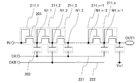
図3に示す電圧調整回路は、単位昇圧回路211_1乃至単位昇圧回路211_n(nは2以上の自然数)を有し、単位昇圧回路211_1乃至単位昇圧回路211_nのそれぞれが直列接続で電気的に接続されたn段の単位昇圧回路を用いて構成される。 3 includes unit booster circuits 211_1 to 211_n (n is a natural number of 2 or more), and the unit booster circuits 211_1 to 211_n are electrically connected in series. It is configured using an n-stage unit booster circuit.
単位昇圧回路211_1乃至単位昇圧回路211_nのそれぞれは、トランジスタ201と、容量素子202と、を有する。
Each of the unit booster circuits 211_1 to 211_n includes a
トランジスタ201としては、チャネル形成層としての機能を有する酸化物半導体層を有するトランジスタを用いることができる。なお、チャネル形成層の水素濃度は、5×10¹⁹atoms/cm3以下、好ましくは5×1018atoms/cm3以下、さらに好ましくは5×1017atoms/cm3以下とする。該水素濃度は、例えば二次イオン質量分析法(SIMS:Secondary Ion Mass Spectroscopy)による値である。またトランジスタ201のキャリア濃度は、1×10¹⁴/cm3以下、好ましくは1×1012/cm3以下とする。
As the
また、単位昇圧回路211_1乃至単位昇圧回路211_nのそれぞれにおいて、トランジスタ201のゲートがトランジスタ201のソース及びドレインの一方に電気的に接続される。すなわち、トランジスタ201はダイオード接続される。また、容量素子202の第1の電極は、トランジスタ201のソース及びドレインの他方に電気的に接続される。
In each of the unit booster circuits 211_1 to 211_n, the gate of the
さらに、K段目(Kは2乃至nの自然数)の単位昇圧回路は、トランジスタ201のソース及びドレインの一方がK−1段目の単位昇圧回路におけるトランジスタ201のソース及びドレインの他方に電気的に接続される。K−1段目の単位昇圧回路におけるトランジスタ201のソース及びドレインの他方と、K段目の単位昇圧回路におけるトランジスタ201のソース及びドレインの一方との接続箇所をノードN1_M(Mは1乃至n/2)という。
Further, in the unit booster circuit of the K-th stage (K is a natural number of 2 to n), one of the source and the drain of the
さらに、2M−1段目(Mは1乃至n/2であり、2Mは自然数)の単位昇圧回路は、容量素子202の第2の電極がクロック信号線221に電気的に接続され、2M段目の単位昇圧回路は、容量素子202の第2の電極がクロック信号線222に電気的に接続される。クロック信号線221にはクロック信号CK1が入力され、クロック信号線222にはクロック信号CKB1が入力される。クロック信号CK1及びクロック信号CKB1は、位相が相反の関係であり、例えばクロック信号CK1がハイレベルのとき、クロック信号CKB1はローレベルである。クロック信号CKB1としては、例えばクロック信号CK1の反転信号を用いることができ、クロック信号CKB1は、例えばインバータなどのNOT回路を用いてクロック信号CK1の電圧状態を反転させることにより生成することができる。クロック信号CK1及びクロック信号CKB1におけるハイレベル及びローレベルの電圧の値は、適宜設定することができる。また、クロック信号CK1は、例えばリングオシレータなどの発振回路とバッファ回路を用いて生成することもできる。また、クロック信号CK1及びクロック信号CKB1のみに限定されず、3相以上のクロック信号を用いることもできる。
Further, in the unit booster circuit of the 2M-1 stage (M is 1 to n / 2, and 2M is a natural number), the second electrode of the
さらに、初段の単位昇圧回路、すなわち単位昇圧回路211_1におけるトランジスタ201は、ソース及びドレインの一方に信号IN1が入力される。
Further, in the first stage unit booster circuit, that is, the
さらに、最終段の単位昇圧回路、すなわち単位昇圧回路211_nにおけるトランジスタ201のソース及びドレインの他方の電圧は、電圧調整回路の出力信号である信号OUT1の電圧となる。また、単位昇圧回路211_nにおける容量素子202は、第2の電極に電圧Vc1が与えられる。電圧Vc1は任意の値でよく、例えば電圧VH又は電圧VLと同じ値の電圧を用いることができる。また、単位昇圧回路211_nにおける容量素子202の容量は、他の単位昇圧回路における容量素子202の容量より大きくすることが好ましい。これにより、単位昇圧回路211_nの出力信号、すなわち電圧調整回路の出力信号である信号OUT1の電圧状態をより安定させることができる。
Further, the other voltage of the source and drain of the
以上のように、本実施の形態の電圧調整回路の一例は、n段の単位昇圧回路を有し、それぞれの単位昇圧回路は、ダイオード接続されたトランジスタと容量素子を有する構成である。ダイオード接続されたトランジスタとしては、チャネル形成層として高純度化された酸化物半導体層を有するトランジスタを用いる。これにより、各ノードの電圧の保持時間を長くすることができ、また、目的の電圧までの到達時間を短くすることができ、電圧変換効率を向上させることができる。 As described above, an example of the voltage adjustment circuit of this embodiment includes an n-stage unit booster circuit, and each unit booster circuit includes a diode-connected transistor and a capacitor. As the diode-connected transistor, a transistor including a highly purified oxide semiconductor layer as a channel formation layer is used. As a result, the voltage holding time of each node can be increased, the arrival time to the target voltage can be shortened, and the voltage conversion efficiency can be improved.
次に、図3に示す電圧調整回路の動作の一例について説明する。 Next, an example of the operation of the voltage adjustment circuit illustrated in FIG. 3 will be described.
図3に示す電圧調整回路の動作は、複数の期間に分けて説明することができる。各期間における動作について以下に説明する。なお、ここで説明する図3に示す電圧調整回路の動作の一例では、信号IN1としてハイレベルの信号が入力され、クロック信号CK1をハイレベル及びローレベルに周期的に変化するクロック信号とし、クロック信号CKB1をクロック信号CKの反転クロック信号とし、各単位昇圧回路におけるトランジスタ201をN型トランジスタとし、各単位昇圧回路におけるトランジスタ201の閾値電圧が同じ値であるとして説明する。
The operation of the voltage regulator circuit illustrated in FIG. 3 can be described by being divided into a plurality of periods. The operation in each period will be described below. Note that in the example of the operation of the voltage adjustment circuit illustrated in FIG. 3 described here, a high-level signal is input as the signal IN1, the clock signal CK1 is a clock signal that periodically changes between a high level and a low level, and the clock In the following description, it is assumed that the signal CKB1 is an inverted clock signal of the clock signal CK, the
まず、第1の期間では、クロック信号CK1がローレベルになり、クロック信号CKB1がハイレベルになる。 First, in the first period, the clock signal CK1 is at a low level and the clock signal CKB1 is at a high level.
このとき、単位昇圧回路211_1において、ダイオード接続されたトランジスタ201が導通状態になり、ノードN1_1の電圧が上昇し始める。ノードN1_1の電圧(電圧VN1ともいう)は、VIN1(信号IN1の電圧)−Vth201(トランジスタ201の閾値電圧)まで上昇する。ノードN1_1の電圧が電圧VIN1−Vth201になると、単位昇圧回路211_1におけるダイオード接続されたトランジスタ201が非導通状態になり、ノードN1_1は浮遊状態になる。
At this time, in the unit booster circuit 211_1, the diode-connected
次に、第2の期間では、クロック信号CK1がハイレベルになり、クロック信号CKB1がローレベルになる。 Next, in the second period, the clock signal CK1 is at a high level and the clock signal CKB1 is at a low level.
このとき、単位昇圧回路211_1において、トランジスタ201は非導通状態に維持され、ノードN1_1は浮遊状態であり、さらに単位昇圧回路211_1における容量素子202の第2の電極に与えられる電圧がVHに変化するため、容量素子202の第2の電極に合わせて容量素子202の第1の電極の電圧も変化し始める。ノードN1_1の電圧は、VIN1−Vth201+VHまで上昇する。このとき、容量素子202の第1の電極と第2の電極の間に印加される電圧は、VIN1−Vth201である。このように、第2の期間において、ノードN1_1の電圧は、第1の期間におけるノードN1_1の電圧が昇圧された値となる。
At this time, in the unit booster circuit 211_1, the
さらに、ノードN1_1の電圧がVIN−Vth201+VHになることにより、単位昇圧回路211_2において、ダイオード接続されたトランジスタ201が導通状態になり、ノードN1_2の電圧が上昇し始める。ノードN1_2の電圧(VN2ともいう)は、VN1−Vth201まで上昇する。ノードN1_2の電圧がVN1−Vth201になると、単位昇圧回路211_2におけるダイオード接続されたトランジスタ201が非導通状態になり、ノードN1_2は浮遊状態になる。
Further, when the voltage of the node N1_1 becomes V IN −V th201 + V H , the diode-connected
次に、第3の期間では、クロック信号CK1がローレベルになり、クロック信号CKB1がハイレベルになる。 Next, in the third period, the clock signal CK1 is at a low level and the clock signal CKB1 is at a high level.
このとき、単位昇圧回路211_2において、トランジスタ201は非導通状態に維持され、ノードN1_2は浮遊状態であり、さらに単位昇圧回路211_2における容量素子202の第2の電極に与えられる電圧がVLからVHに変化するため、容量素子202の第2の電極に合わせて容量素子202の第1の電極の電圧も変化し始める。ノードN1_2の電圧は、VN1−Vth201+VHまで上昇する。このとき、容量素子202の第1の電極と第2の電極の間に印加される電圧は、VN1−Vth201である。このように、第3の期間において、ノードN1_2の電圧は、第2の期間におけるノードN1_2の電圧が昇圧された値となる。
At this time, in the unit booster circuit 211_2, the
さらに、ノードN1_2の電圧がVN1−Vth201+VHになることにより、単位昇圧回路211_3において、ダイオード接続されたトランジスタ201が導通状態になり、ノードN1_3の電圧が上昇し始める。ノードN1_3の電圧(VN3ともいう)は、VN2−Vth201まで上昇する。ノードN1_3の電圧がVN2−Vth201になると、単位昇圧回路211_3におけるダイオード接続されたトランジスタ201が非導通状態になり、ノードN1_3は浮遊状態になる。
Further, when the voltage of the node N1_2 becomes V N1 −V th201 + V H , the diode-connected
さらに、3段目以降の各単位昇圧回路においてもクロック信号CK1又はクロック信号CKB1がハイレベル又はローレベルに周期的に変化するに従って上記単位昇圧回路と同様の動作が順次行われ、各ノードN1_Mの電圧は、クロック信号CK1又はクロック信号CKB1がハイレベル又はローレベルに周期的に変化する毎に徐々に昇圧され、最大でVIN1+M(VH−Vth201)に昇圧される。また、信号OUT1の電圧は、クロック信号CK1又はクロック信号CKB1がハイレベル又はローレベルに周期的に変化する毎に徐々に昇圧され、最大でVIN1+n(VH−Vth201)に昇圧される。このように、図3に示す電圧調整回路は、信号IN1の電圧を昇圧し、昇圧した電圧の信号OUT1を出力信号として出力する。 Further, in each unit booster circuit in the third and subsequent stages, the same operation as that of the unit booster circuit is sequentially performed as the clock signal CK1 or the clock signal CKB1 periodically changes to a high level or a low level, and each node N1_M The voltage is gradually increased every time the clock signal CK1 or the clock signal CKB1 periodically changes to a high level or a low level, and is increased to V IN1 + M (V H −V th201 ) at the maximum. The voltage of the signal OUT1 is gradually increased every time the clock signal CK1 or the clock signal CKB1 periodically changes to a high level or a low level, and is increased to a maximum of V IN1 + n (V H −V th201 ). . 3 boosts the voltage of the signal IN1, and outputs the boosted voltage signal OUT1 as an output signal.
以上のように、本実施の形態の電圧調整回路の一例では、各単位昇圧回路において昇圧動作を行うことにより、入力された信号の電圧より大きい電圧の信号を出力信号として出力することができる。 As described above, in the example of the voltage adjustment circuit of this embodiment, by performing a boosting operation in each unit booster circuit, a signal having a voltage higher than the voltage of the input signal can be output as an output signal.
また、本実施の形態の電圧調整回路の一例は、各単位昇圧回路においてダイオード接続されたトランジスタが、チャネル形成層として高純度化された酸化物半導体層を用いたトランジスタである構成である。これによりトランジスタのリーク電流を低減し、所望の電圧への変換効率を向上させることができ、各ノードの電圧の保持期間を長くすることができ、また昇圧動作により所望の電圧となるまでの到達速度を速くすることができる。 In addition, an example of the voltage regulator circuit in this embodiment is a structure in which a diode-connected transistor in each unit booster circuit is a transistor using a highly purified oxide semiconductor layer as a channel formation layer. As a result, the leakage current of the transistor can be reduced, the conversion efficiency to a desired voltage can be improved, the voltage holding period of each node can be lengthened, and the voltage reaches the desired voltage by the boosting operation. Speed can be increased.
なお、本実施の形態は、他の実施の形態と適宜組み合わせることができる。 Note that this embodiment can be combined with any of the other embodiments as appropriate.
(実施の形態3)
本実施の形態では、本発明の一態様である電圧調整回路の他の一例として降圧回路について説明する。なお本実施の形態において、実施の形態2に示す電圧調整回路と同じ部分については、説明を適宜援用する。
(Embodiment 3)
In this embodiment, a step-down circuit will be described as another example of the voltage regulator circuit which is one embodiment of the present invention. Note that in this embodiment, the description of the same portions as those of the voltage regulator circuit described in
本実施の形態の電圧調整回路の回路構成の一例について図4を用いて説明する。図4は、本実施の形態の電圧調整回路の回路構成の一例を示す回路図である。 An example of a circuit configuration of the voltage regulator circuit of this embodiment will be described with reference to FIG. FIG. 4 is a circuit diagram showing an example of the circuit configuration of the voltage adjustment circuit of the present embodiment.
図4に示す電圧調整回路は、単位降圧回路511_1乃至単位降圧回路511_n(nは2以上の自然数)を有し、単位降圧回路511_1乃至単位降圧回路511_nのそれぞれが直列接続で電気的に接続されたn段の単位降圧回路により構成される。 4 includes unit step-down circuits 511_1 to unit step-down circuits 511_n (n is a natural number equal to or greater than 2), and the unit step-down circuits 511_1 to unit step-down circuits 511_n are electrically connected in series. In addition, it is configured by an n-stage unit step-down circuit.
単位降圧回路511_1乃至単位降圧回路511_nのそれぞれは、トランジスタ501と、容量素子502と、を有する。
Each of the unit step-down circuits 511_1 to 511_n includes a
トランジスタ501としては、チャネル形成層としての機能を有する酸化物半導体層を有するトランジスタを用いることができる。なお、チャネル形成層の水素濃度は、5×10¹⁹atoms/cm3以下、好ましくは5×1018atoms/cm3以下、さらに好ましくは5×1017atoms/cm3以下とする。該水素濃度は、例えば二次イオン質量分析法(SIMS:Secondary Ion Mass Spectroscopy)による値である。また、トランジスタ501のキャリア濃度は、1×10¹⁴/cm3以下、好ましくは1×1012/cm3以下とする。
As the
K段目(Kは2乃至nの自然数)の単位降圧回路は、トランジスタ501のソース及びドレインの一方がK−1段目の単位降圧回路におけるトランジスタ501のソース及びドレインの他方に電気的に接続される。K−1段目の単位降圧回路におけるトランジスタ501のソース及びドレインの他方と、K段目の単位降圧回路におけるトランジスタ501のソース及びドレインの一方との接続箇所をノードN2_Mという。
In the unit step-down circuit of the K-th stage (K is a natural number of 2 to n), one of the source and the drain of the
また、単位降圧回路511_1乃至単位降圧回路511_nのそれぞれにおいて、トランジスタ501のゲートがトランジスタ501のソース及びドレインの他方に電気的に接続される。すなわちトランジスタ501はダイオード接続される。また、容量素子502の第1の電極は、トランジスタ501のソース及びドレインの他方に電気的に接続される。すなわち、図3に示す電圧調整回路におけるトランジスタ201は、ゲートと、ソース及びドレインの一方とが電気的に接続される構成であるのに対し、図4に示す電圧調整回路におけるトランジスタ501は、ゲートと、ソース及びドレインの他方とが電気的に接続される。
In each of the unit voltage step-down circuits 511_1 to 511_n, the gate of the
さらに、2M−1段目の単位降圧回路は、容量素子502の第1の電極がトランジスタ501のゲートに電気的に接続され、第2の電極がクロック信号線521に電気的に接続され、2M段目の単位降圧回路は、トランジスタ501のソース及びドレインの一方が2M−1段目におけるトランジスタ501のゲート、及びソース又はドレインの電気的に接続され、容量素子502の第1の電極がトランジスタ501のゲート、並びにソース及びドレインの他方に電気的に接続され、第2の電極がクロック信号線522に電気的に接続される。クロック信号線521にはクロック信号CK2が入力され、クロック信号線522にはクロック信号CKB2が入力される。クロック信号CK2及びクロック信号CKB2は、位相が相反の関係であり、例えばクロック信号CK2がハイレベルのとき、クロック信号CKB2はローレベルである。クロック信号CKB2としては、例えばクロック信号CK2の反転信号を用いることができ、クロック信号CKB2は、例えばインバータなどのNOT回路を用いてクロック信号CK2の電圧状態を反転させることにより生成することができる。クロック信号CK2及びクロック信号CKB2におけるハイレベル及びローレベルの電圧の値は、適宜設定することができる。また、クロック信号CK2は、例えばリングオシレータなどの発振回路とバッファ回路を用いて生成することもできる。また、クロック信号CK2及びクロック信号CKB2のみに限定されず、3相以上のクロック信号を用いることもできる。
Further, in the unit step-down circuit in the 2M−1 stage, the first electrode of the
さらに、初段の単位降圧回路、すなわち単位降圧回路511_1におけるトランジスタ501は、ソース及びドレインの一方に信号IN2が入力される。
Further, the signal IN2 is input to one of a source and a drain of the
さらに、最終段の単位降圧回路、すなわち単位降圧回路511_nにおけるトランジスタ501のソース及びドレインの他方の電圧は、電圧調整回路の出力信号である信号OUT2の電圧となる。また、単位降圧回路511_nにおける容量素子502は、第2の電極に電圧Vc2が与えられる。電圧Vc2は任意の値でよく、例えば電圧VH又は電圧VLと同じ値の電圧を用いることができる。また、単位降圧回路511_nにおける容量素子502の容量は、他の単位降圧回路における容量素子502の容量より大きくすることが好ましい。これにより、単位降圧回路511_nの出力信号、すなわち電圧調整回路の出力信号である信号OUT2の電圧状態をより安定させることができる。
Further, the other voltage of the source and drain of the
以上のように、本実施の形態の電圧調整回路の一例は、n段の単位降圧回路を有し、それぞれの単位降圧回路は、ダイオード接続されたトランジスタと容量素子を有する構成である。ダイオード接続されたトランジスタとしては、チャネル形成層として水素濃度を低減し、オフ電流を低減した酸化物半導体層を有するトランジスタを用いる。これにより、各ノードの電圧の保持時間を長くすることができ、また、目的の電圧までの到達時間を短くすることができ、電圧変換効率を向上させることができる。 As described above, an example of the voltage regulator circuit according to this embodiment includes an n-stage unit voltage step-down circuit, and each unit voltage step-down circuit includes a diode-connected transistor and a capacitor. As the diode-connected transistor, a transistor including an oxide semiconductor layer in which the hydrogen concentration is reduced and the off-state current is reduced is used as a channel formation layer. As a result, the voltage holding time of each node can be increased, the arrival time to the target voltage can be shortened, and the voltage conversion efficiency can be improved.
次に、図4に示す電圧調整回路の動作の一例について説明する。 Next, an example of the operation of the voltage adjustment circuit illustrated in FIG. 4 will be described.
図4に示す電圧調整回路の動作は、複数の期間に分けて説明することができる。各期間における動作について以下に説明する。なお、ここで説明する図4に示す電圧調整回路の動作の一例では、信号IN2としてローレベルの信号が入力され、クロック信号CK2をハイレベル及びローレベルに周期的に変化するクロック信号とし、クロック信号CKB2をクロック信号CK2の反転クロック信号とし、各単位降圧回路におけるトランジスタ501をN型トランジスタとし、各単位降圧回路におけるトランジスタ501の閾値電圧は同じ値であるとして説明する。
The operation of the voltage regulator circuit illustrated in FIG. 4 can be described by being divided into a plurality of periods. The operation in each period will be described below. Note that in the example of the operation of the voltage adjustment circuit illustrated in FIG. 4 described here, a low level signal is input as the signal IN2, the clock signal CK2 is a clock signal that periodically changes between a high level and a low level, and the clock In the following description, it is assumed that the signal CKB2 is an inverted clock signal of the clock signal CK2, the
まず、第1の期間では、クロック信号CK2がハイレベルになり、クロック信号CKB2がローレベルになる。 First, in the first period, the clock signal CK2 becomes high level and the clock signal CKB2 becomes low level.
このとき、単位降圧回路511_1において、ダイオード接続されたトランジスタ501が導通状態になり、ノードN2_1の電圧が下降し始める。ノードN2_1の電圧(電圧VN2ともいう)は、VIN2(信号IN2の電圧)+Vth501(トランジスタ501の閾値電圧)まで下降する。ノードN2_1の電圧が電圧VIN2+Vth501になると、単位降圧回路511_1におけるダイオード接続されたトランジスタ501が非導通状態になり、ノードN2_1は浮遊状態になる。
At this time, in the unit step-down circuit 511_1, the diode-connected
次に、第2の期間では、クロック信号CK2がローレベルになり、クロック信号CKB2がハイレベルになる。 Next, in the second period, the clock signal CK2 is at a low level and the clock signal CKB2 is at a high level.
このとき、単位降圧回路511_1において、トランジスタ501は、非導通状態に維持され、ノードN2_1は浮遊状態であり、さらに単位降圧回路511_1における容量素子502の第2の電極に与えられる電圧がVLに変化するため、容量素子502の第2の電極に合わせて容量素子502の第1の電極の電圧も変化し始める。ノードN2_1の電圧は、VIN2+Vth501−VHまで下降する。このとき、容量素子502の第1の電極と第2の電極の間に印加される電圧は、VIN2+Vth501である。このように、第2の期間において、ノードN2_1の電圧は、第1の期間におけるノードN2_1の電圧が降圧された値となる。
At this time, in the unit step-down circuit 511_1, the
さらに、ノードN2_1の電圧がVIN2+Vth501−VHになることにより、単位降圧回路511_2において、ダイオード接続されたトランジスタ501が導通状態になり、ノードN2_2の電圧が下降し始める。ノードN2_2の電圧(VN2ともいう)は、VN2+Vth501まで下降する。ノードN2_2の電圧がVN2+Vth501になると、単位降圧回路511_2におけるダイオード接続されたトランジスタ501が非導通状態になり、ノードN2_2は浮遊状態になる。
Further, by the voltage of the node N2_1 is V IN2 + V th501 -V H, in the unit step-down circuit 511_2, becomes a diode-connected
次に、第3の期間では、クロック信号CK2がハイレベルになり、クロック信号CKB2がローレベルになる。 Next, in the third period, the clock signal CK2 becomes high level and the clock signal CKB2 becomes low level.
このとき、単位降圧回路511_2において、トランジスタ501は非導通状態に維持され、ノードN2_2は浮遊状態であり、さらに単位降圧回路511_2における容量素子502の第2の電極に与えられる電圧がVLに変化するため、容量素子502の第2の電極に合わせて容量素子502の第1の電極の電圧も変化し始める。ノードN2_2の電圧は、VN2+Vth501−VHまで下降する。このとき、容量素子502の第1の電極と第2の電極の間に印加される電圧は、VN2+Vth501である。このように、第3の期間において、ノードN2_2の電圧は、第2の期間におけるノードN2_2の電圧が降圧された値となる。
At this time, in the unit step-down circuit 511_2, the
さらに、ノードN2_2の電圧がVN2+Vth501−VHになることにより、単位降圧回路511_3において、ダイオード接続されたトランジスタ501が導通状態になり、ノードN2_3の電圧が下降し始める。ノードN2_3の電圧(VN3ともいう)は、VN2+Vth501まで下降する。ノードN2_3の電圧がVN2+Vth501になると、単位降圧回路511_3におけるダイオード接続されたトランジスタ501が非導通状態になり、ノードN2_3は浮遊状態になる。
Further, when the voltage at the node N2_2 becomes V N2 + V th501 -V H , the diode-connected
さらに、3段目以降の各単位降圧回路においてもクロック信号CK2又はクロック信号CKB2がハイレベル又はローレベルに周期的に変化するに従って上記単位降圧回路と同様の動作が順次行われ、各ノードN2_Mの電圧のそれぞれは、クロック信号CK2又はクロック信号CKB2がハイレベル又はローレベルに周期的に変化する毎に徐々に降圧され、最小でVIN2−M(VH+Vth501)となる。また、信号OUT2の電圧は、クロック信号CK2又はクロック信号CKB2がハイレベル又はローレベルに周期的に変化する毎に徐々に降圧され、最小でVIN2−n(VH+Vth501)となる。このように、図4に示す電圧調整回路は、信号IN2の電圧が降圧された電圧の信号OUT2を出力信号として出力する。 Further, in each unit step-down circuit after the third stage, the same operation as that of the unit step-down circuit is sequentially performed as the clock signal CK2 or the clock signal CKB2 periodically changes to the high level or the low level, and the node N2_M Each of the voltages is gradually stepped down every time the clock signal CK2 or the clock signal CKB2 periodically changes to a high level or a low level, and becomes V IN2 −M (V H + V th501 ) at the minimum. In addition, the voltage of the signal OUT2 is gradually reduced every time the clock signal CK2 or the clock signal CKB2 periodically changes to a high level or a low level, and becomes the minimum V IN2 −n (V H + V th501 ). As described above, the voltage adjustment circuit illustrated in FIG. 4 outputs the signal OUT2 having a voltage obtained by stepping down the voltage of the signal IN2 as an output signal.
以上のように、本実施の形態の電圧調整回路の一例は、各単位降圧回路において降圧動作を行うことにより、入力された信号の電圧より小さい電圧の信号を出力信号として出力することができる。 As described above, an example of the voltage adjustment circuit of this embodiment can output a signal having a voltage smaller than the voltage of the input signal as an output signal by performing a step-down operation in each unit step-down circuit.
また、本実施の形態の電圧調整回路の一例は、各単位降圧回路においてダイオード接続されたトランジスタが、チャネル形成層として高純度化された酸化物半導体層を用いたトランジスタである構成である。これにより、トランジスタのリーク電流を低減し、所望の電圧への変換効率を向上させることができ、各ノードの電圧の保持期間を長くすることができ、また降圧動作により所望の電圧となるまでの到達速度を速くすることができる。 In addition, an example of the voltage regulator circuit in this embodiment has a structure in which a diode-connected transistor in each unit step-down circuit is a transistor using a highly purified oxide semiconductor layer as a channel formation layer. As a result, the leakage current of the transistor can be reduced, the conversion efficiency to a desired voltage can be improved, the voltage holding period of each node can be lengthened, and the voltage until the desired voltage is obtained by the step-down operation. The arrival speed can be increased.
なお、本実施の形態は、他の実施の形態と適宜組み合わせることができる。 Note that this embodiment can be combined with any of the other embodiments as appropriate.
(実施の形態4)
本実施の形態は、本明細書で開示する電圧調整回路を構成するトランジスタに適用できる薄膜トランジスタの例を示す。
(Embodiment 4)
This embodiment shows an example of a thin film transistor which can be applied to a transistor included in the voltage regulator circuit disclosed in this specification.
本実施の形態のトランジスタ及びトランジスタの作製方法の一形態を、図5及び図6を用いて説明する。 One embodiment of a transistor and a method for manufacturing the transistor of this embodiment will be described with reference to FIGS.
図5(A)(B)にトランジスタの平面及び断面構造の一例を示す。図5(A)(B)に示す薄膜トランジスタ410は、トップゲート構造の薄膜トランジスタの一つである。
FIGS. 5A and 5B illustrate an example of a plan view and a cross-sectional structure of a transistor. A
図5(A)はトップゲート構造の薄膜トランジスタ410の平面図であり、図5(B)は図5(A)の線C1−C2における断面図である。
5A is a plan view of the top-gate
薄膜トランジスタ410は、絶縁表面を有する基板400上に、絶縁層407、酸化物半導体層412、ソース電極層又はドレイン電極層415a、及びソース電極層又はドレイン電極層415b、ゲート絶縁層402、ゲート電極層411を含み、ソース電極層又はドレイン電極層415a、ソース電極層又はドレイン電極層415bにそれぞれ配線層414a、配線層414bが接して設けられ電気的に接続している。
The
また、薄膜トランジスタ410はシングルゲート構造の薄膜トランジスタを用いて説明するが、必要に応じて、チャネル形成領域を複数有するマルチゲート構造の薄膜トランジスタも形成することができる。
Although the
以下、図6(A)乃至(E)を用い、基板400上に薄膜トランジスタ410を作製する工程を説明する。
Hereinafter, a process for manufacturing the
絶縁表面を有する基板400に使用することができる基板に大きな制限はないが、少なくとも、後の加熱処理に耐えうる程度の耐熱性を有していることが必要となる。バリウムホウケイ酸ガラスやアルミノホウケイ酸ガラスなどのガラス基板を用いることができる。
There is no particular limitation on a substrate that can be used as the
また、ガラス基板としては、後の加熱処理の温度が高い場合には、歪み点が730℃以上のものを用いると良い。また、ガラス基板には、例えば、アルミノシリケートガラス、アルミノホウケイ酸ガラス、バリウムホウケイ酸ガラスなどのガラス材料が用いられている。なお、酸化ホウ素と比較して酸化バリウム(BaO)を多く含ませることで、より実用的な耐熱ガラスが得られる。このため、B2O3よりBaOを多く含むガラス基板を用いることが好ましい As the glass substrate, a glass substrate having a strain point of 730 ° C. or higher is preferably used when the temperature of the subsequent heat treatment is high. For the glass substrate, for example, a glass material such as aluminosilicate glass, aluminoborosilicate glass, or barium borosilicate glass is used. Note that a more practical heat-resistant glass can be obtained by containing more barium oxide (BaO) than boron oxide. For this reason, it is preferable to use a glass substrate containing more BaO than B 2 O 3.
なお、上記のガラス基板に代えて、セラミック基板、石英基板、サファイア基板などの絶縁体でなる基板を用いても良い。他にも、結晶化ガラスなどを用いることができる。また、プラスチック基板等も適宜用いることができる。また基板としてシリコンなどの半導体基板を用いることもできる。 Note that a substrate formed of an insulator such as a ceramic substrate, a quartz substrate, or a sapphire substrate may be used instead of the glass substrate. In addition, crystallized glass or the like can be used. A plastic substrate or the like can also be used as appropriate. A semiconductor substrate such as silicon can also be used as the substrate.
まず、絶縁表面を有する基板400上に下地膜となる絶縁層407を形成する。酸化物半導体層と接する絶縁層407は、酸化シリコン層、酸化窒化シリコン層、酸化アルミニウム層、又は酸化窒化アルミニウム層などの酸化物絶縁層を用いると好ましい。絶縁層407の形成方法としては、プラズマCVD法又はスパッタリング法等を用いることができるが、絶縁層407中に水素が多量に含まれないようにするためには、スパッタリング法で絶縁層407を成膜することが好ましい。
First, the insulating
本実施の形態では、絶縁層407として、スパッタリング法により酸化シリコン層を形成する。基板400を処理室へ搬送し、水素及び水分が除去された酸素を含む高純度スパッタガスを導入しシリコン半導体のターゲットを用いて、基板400に絶縁層407として、酸化シリコン層を成膜する。また基板400は室温でもよいし、加熱されていてもよい。
In this embodiment, a silicon oxide layer is formed as the insulating
例えば、石英(好ましくは合成石英)をターゲットとして用い、基板温度108℃、基板とターゲットの間との距離(T−S間距離)を60mm、圧力0.4Pa、高周波電源1.5kW、酸素及びアルゴン(酸素流量25sccm:アルゴン流量25sccm=1:1)雰囲気下でRFスパッタリング法により酸化シリコン膜を成膜する。膜厚は100nmとする。なお、石英(好ましくは合成石英)に代えてシリコンターゲットを酸化シリコン膜を成膜するためのターゲットとして用いることができる。なお、スパッタガスとして酸素又は、酸素及びアルゴンの混合ガスを用いる。 For example, quartz (preferably synthetic quartz) is used as a target, the substrate temperature is 108 ° C., the distance between the substrate and the target (T-S distance) is 60 mm, the pressure is 0.4 Pa, the high frequency power supply is 1.5 kW, oxygen and A silicon oxide film is formed by an RF sputtering method in an atmosphere of argon (oxygen flow rate 25 sccm: argon flow rate 25 sccm = 1: 1). The film thickness is 100 nm. Note that instead of quartz (preferably synthetic quartz), a silicon target can be used as a target for forming a silicon oxide film. Note that oxygen or a mixed gas of oxygen and argon is used as a sputtering gas.
この場合において、処理室内の残留水分を除去しつつ絶縁層407を成膜することが好ましい。絶縁層407に水素、水酸基又は水分が含まれないようにするためである。
In this case, it is preferable to form the insulating
処理室内の残留水分を除去するためには、吸着型の真空ポンプを用いることが好ましい。例えば、クライオポンプ、イオンポンプ、チタンサブリメーションポンプを用いることが好ましい。また、排気手段としては、ターボポンプにコールドトラップを加えたものであってもよい。クライオポンプを用いて排気した成膜室は、例えば、水素原子や、水(H2O)など水素原子を含む化合物等が排気されるため、当該成膜室で成膜した絶縁層407に含まれる不純物の濃度を低減できる。
In order to remove moisture remaining in the treatment chamber, an adsorption-type vacuum pump is preferably used. For example, it is preferable to use a cryopump, an ion pump, or a titanium sublimation pump. The exhaust means may be a turbo pump provided with a cold trap. The film formation chamber evacuated using a cryopump is included in the insulating
絶縁層407を成膜する際に用いるスパッタガスは、水素、水、水酸基又は水素化物などの不純物が、数濃度ppm程度、数濃度ppb程度まで除去された高純度ガスを用いることが好ましい。
As a sputtering gas used for forming the insulating
スパッタリング法としては、例えばスパッタ用電源に高周波電源を用いるRFスパッタリング法、直流電源を用いるDCスパッタリング法、又はパルス的にバイアスを与えるパルスDCスパッタリング法などがある。RFスパッタリング法は主に絶縁膜を成膜する場合に用いられ、DCスパッタリング法は主に金属膜を成膜する場合に用いられる。 Examples of the sputtering method include an RF sputtering method using a high frequency power source as a sputtering power source, a DC sputtering method using a DC power source, or a pulse DC sputtering method that applies a bias in a pulsed manner. The RF sputtering method is mainly used when an insulating film is formed, and the DC sputtering method is mainly used when a metal film is formed.
また、材料の異なるターゲットを複数設置できる多元スパッタ装置もある。多元スパッタ装置は、同一チャンバーで異なる材料膜を積層成膜することも、同一チャンバーで複数種類の材料を同時に放電させて成膜することもできる。 There is also a multi-source sputtering apparatus in which a plurality of targets of different materials can be installed. The multi-source sputtering apparatus can be formed by stacking different material films in the same chamber, or by simultaneously discharging a plurality of types of materials in the same chamber.
また、チャンバー内部に磁石機構を備えたマグネトロンスパッタリング法を用いるスパッタ装置や、グロー放電を使わずマイクロ波を用いて発生させたプラズマを用いるECRスパッタリング法を用いるスパッタ装置がある。 Further, there are a sputtering apparatus using a magnetron sputtering method having a magnet mechanism inside a chamber, and a sputtering apparatus using an ECR sputtering method using plasma generated using microwaves without using glow discharge.
また、スパッタリング法を用いる成膜方法として、成膜中にターゲット物質とスパッタガス成分とを化学反応させてそれらの化合物薄膜を形成するリアクティブスパッタリング法や、成膜中に基板にも電圧をかけるバイアススパッタリング法もある。 In addition, as a film formation method using a sputtering method, a reactive sputtering method in which a target material and a sputtering gas component are chemically reacted during film formation to form a compound thin film thereof, or a voltage is applied to the substrate during film formation. There is also a bias sputtering method.
また、絶縁層407は積層構造でもよく、例えば、基板400側から窒化シリコン層、窒化酸化シリコン層、窒化アルミニウム層、又は窒化酸化アルミニウムなどの窒化物絶縁層と、上記酸化物絶縁層との積層構造としてもよい。
The insulating
例えば、水素及び水分が除去された窒素を含む高純度のスパッタガスを導入しシリコンターゲットを用いて酸化シリコン層と基板との間に窒化シリコン層を成膜する。この場合においても、酸化シリコン層と同様に、処理室内の残留水分を除去しつつ窒化シリコン層を成膜することが好ましい。 For example, a high-purity sputtering gas containing nitrogen from which hydrogen and moisture have been removed is introduced, and a silicon nitride layer is formed between the silicon oxide layer and the substrate using a silicon target. Also in this case, it is preferable to form the silicon nitride layer while removing residual moisture in the treatment chamber, as in the case of the silicon oxide layer.
窒化シリコン層を形成する場合も、成膜時に基板を加熱してもよい。 In the case of forming a silicon nitride layer, the substrate may be heated at the time of film formation.
絶縁層407として窒化シリコン層と酸化シリコン層とを積層する場合、窒化シリコン層と酸化シリコン層を同じ処理室において、共通のシリコンターゲットを用いて成膜することができる。先に窒素を含むスパッタガスを導入して、処理室内に装着されたシリコンターゲットを用いて窒化シリコン層を形成し、次にスパッタガスを酸素を含むスパッタガスに切り替えて同じシリコンターゲットを用いて酸化シリコン層を成膜する。窒化シリコン層と酸化シリコン層とを大気に曝露せずに連続して形成することができるため、窒化シリコン層表面に水素や水分などの不純物が吸着することを防止することができる。
In the case where a silicon nitride layer and a silicon oxide layer are stacked as the insulating
次いで、絶縁層407上に、膜厚2nm以上200nm以下の酸化物半導体膜を形成する。
Next, an oxide semiconductor film with a thickness of 2 nm to 200 nm is formed over the insulating
また、酸化物半導体膜に水素、水酸基及び水分がなるべく含まれないようにするために、成膜の前処理として、スパッタリング装置の予備加熱室で絶縁層407が形成された基板400を予備加熱し、基板400に吸着した水素、水分などの不純物を脱離し排気することが好ましい。なお、予備加熱室に設ける排気手段はクライオポンプが好ましい。なお、この予備加熱の処理は省略することもできる。またこの予備加熱は、後に形成するゲート絶縁層402の成膜前の基板400に行ってもよいし、後に形成するソース電極層又はドレイン電極層415a及びソース電極層又はドレイン電極層415bまで形成した基板400にも同様に行ってもよい。
In order to prevent the oxide semiconductor film from containing hydrogen, a hydroxyl group, and moisture as much as possible, as a pretreatment for film formation, the
なお、酸化物半導体膜をスパッタリング法により成膜する前に、アルゴンガスを導入し、プラズマを発生させて逆スパッタを行い、絶縁層407の表面に付着しているゴミを除去することが好ましい。逆スパッタとは、ターゲット側に電圧を印加せずに、アルゴン雰囲気下で基板側に高周波電源を用いて電圧を印加してプラズマを形成して表面を改質する方法である。なお、アルゴン雰囲気に代えて窒素、ヘリウム、酸素などを用いてもよい。
Note that before the oxide semiconductor film is formed by a sputtering method, it is preferable to introduce argon gas, generate plasma, and perform reverse sputtering to remove dust attached to the surface of the insulating
酸化物半導体膜はスパッタリング法により成膜する。酸化物半導体膜は、In−Ga−Zn−O系、In−Sn−Zn−O系、In−Al−Zn−O系、Sn−Ga−Zn−O系、Al−Ga−Zn−O系、Sn−Al−Zn−O系、In−Zn−O系、Sn−Zn−O系、Al−Zn−O系、In−O系、In−Sn−O系、Sn−O系、Zn−O系の酸化物半導体膜を用いる。本実施の形態では、酸化物半導体膜をIn−Ga−Zn−O系金属酸化物ターゲットを用いてスパッタリング法により成膜する。また、酸化物半導体膜は、希ガス(代表的にはアルゴン)雰囲気下、酸素雰囲気下、又は希ガス(代表的にはアルゴン)及び酸素雰囲気下においてスパッタリング法により形成することができる。また、スパッタリング法を用いる場合、SiO2を2重量%以上10重量%以下含むターゲットを用いて成膜を行ってもよい。 The oxide semiconductor film is formed by a sputtering method. An oxide semiconductor film includes an In—Ga—Zn—O system, an In—Sn—Zn—O system, an In—Al—Zn—O system, a Sn—Ga—Zn—O system, and an Al—Ga—Zn—O system. Sn-Al-Zn-O-based, In-Zn-O-based, Sn-Zn-O-based, Al-Zn-O-based, In-O-based, In-Sn-O-based, Sn-O-based, Zn- An O-based oxide semiconductor film is used. In this embodiment, the oxide semiconductor film is formed by a sputtering method with the use of an In—Ga—Zn—O-based metal oxide target. The oxide semiconductor film can be formed by a sputtering method in a rare gas (typically argon) atmosphere, an oxygen atmosphere, or a rare gas (typically argon) and oxygen atmosphere. In the case where the sputtering method is used, the film may be formed using a target containing 2 wt% or more and 10 wt% or less of SiO 2 .
酸化物半導体膜を、成膜する際に用いるスパッタガスは水素、水、水酸基又は水素化物などの不純物が、数濃度ppm程度、数濃度ppb程度まで除去された高純度ガスを用いることが好ましい。 As a sputtering gas used for forming the oxide semiconductor film, it is preferable to use a high-purity gas from which impurities such as hydrogen, water, a hydroxyl group, or a hydride are removed to about several ppm and several ppb.
酸化物半導体膜をスパッタリング法で作製するためのターゲットとして、酸化亜鉛を主成分とする金属酸化物のターゲットを用いることができる。また、金属酸化物のターゲットの他の例としては、例えば、In2O3:Ga2O3:ZnO=1:1:1[mol数比]の組成比である金属酸化物ターゲットを用いることができる。また、上記に示すターゲットに限定されず、例えば、In2O3:Ga2O3:ZnO=1:1:2[mol数比]の組成比である金属酸化物ターゲットを用いてもよい。また、作製される金属酸化物ターゲットのうち、全体の体積に対して全体の体積から空隙などが占める空間を除いた部分の体積の割合(充填率ともいう)は、90%以上100%以下、好ましくは95%以上99.9%以下である。充填率の高い金属酸化物ターゲットを用いることにより形成した酸化物半導体膜は、緻密な膜となる。 As a target for forming the oxide semiconductor film by a sputtering method, a metal oxide target containing zinc oxide as a main component can be used. In addition, as another example of the metal oxide target, for example, a metal oxide target having a composition ratio of In 2 O 3 : Ga 2 O 3 : ZnO = 1: 1: 1 [molar ratio] is used. Can do. Further, the present invention is not limited to the above target, and for example, a metal oxide target having a composition ratio of In 2 O 3 : Ga 2 O 3 : ZnO = 1: 1: 2 [molar ratio] may be used. Further, in the metal oxide target to be produced, the ratio of the volume of the portion excluding the space occupied by voids from the entire volume (also referred to as the filling rate) with respect to the entire volume is 90% or more and 100% or less, Preferably they are 95% or more and 99.9% or less. An oxide semiconductor film formed by using a metal oxide target with a high filling rate is a dense film.
減圧状態に設定された処理室内に基板を保持し、処理室内の残留水分を除去しつつ水素及び水分が除去されたスパッタガスを導入し、金属酸化物をターゲットとして基板400上に酸化物半導体膜を成膜する。処理室内の残留水分を除去するためには、吸着型の真空ポンプを用いることが好ましい。例えば、クライオポンプ、イオンポンプ、チタンサブリメーションポンプを用いることが好ましい。また、排気手段としては、ターボポンプにコールドトラップを加えたものであってもよい。クライオポンプを用いて排気した成膜室は、例えば、水素原子、水(H2O)など水素原子を含む化合物(より好ましくは炭素原子を含む化合物も)等が排気されるため、当該成膜室で成膜した酸化物半導体膜に含まれる不純物の濃度を低減できる。また、酸化物半導体膜成膜時に基板を加熱してもよい。
The substrate is held in a processing chamber set in a reduced pressure state, a sputtering gas from which hydrogen and moisture have been removed is introduced while removing residual moisture in the processing chamber, and an oxide semiconductor film is formed over the
成膜条件の一例としては、基板温度室温、基板とターゲットの間との距離を60mm、圧力0.4Pa、直流(DC)電源0.5kW、酸素及びアルゴン(酸素流量15sccm:アルゴン流量30sccm=1:2)雰囲気下の条件が適用される。なお、パルス直流(DC)電源を用いると、成膜時に発生する粉状物質(パーティクル、ゴミともいう)が軽減でき、膜厚分布も均一となるために好ましい。酸化物半導体膜は好ましくは5nm以上30nm以下とする。なお、適用する酸化物半導体材料により適切な厚みは異なり、材料に応じて適宜厚みを選択すればよい。 As an example of film formation conditions, the substrate temperature is room temperature, the distance between the substrate and the target is 60 mm, the pressure is 0.4 Pa, the direct current (DC) power source is 0.5 kW, oxygen and argon (oxygen flow rate 15 sccm: argon flow rate 30 sccm = 1). : 2) Conditions under atmosphere are applied. Note that a pulse direct current (DC) power source is preferable because powder substances (also referred to as particles or dust) generated in film formation can be reduced and the film thickness can be uniform. The oxide semiconductor film is preferably 5 nm to 30 nm. Note that an appropriate thickness differs depending on an oxide semiconductor material to be used, and the thickness may be selected as appropriate depending on the material.
次いで、酸化物半導体膜を第1のフォトリソグラフィ工程により島状の酸化物半導体層412に加工する(図6(A)参照。)。また、島状の酸化物半導体層412を形成するためのレジストマスクをインクジェット法で形成してもよい。レジストマスクをインクジェット法で形成するとフォトマスクを使用しないため、製造コストを低減できる。
Next, the oxide semiconductor film is processed into an island-shaped
なお、ここでの酸化物半導体膜のエッチングは、ドライエッチングでもウェットエッチングでもよく、両方を用いてもよい。 Note that the etching of the oxide semiconductor film here may be either dry etching or wet etching, or both.
ドライエッチングに用いるエッチングガスとしては、塩素を含むガス(塩素系ガス、例えば塩素(Cl2)、塩化硼素(BCl3)、塩化珪素(SiCl4)、四塩化炭素(CCl4)など)が好ましい。 As an etching gas used for dry etching, a gas containing chlorine (chlorine-based gas such as chlorine (Cl 2 ), boron chloride (BCl 3 ), silicon chloride (SiCl 4 ), carbon tetrachloride (CCl 4 ), or the like) is preferable. .
また、フッ素を含むガス(フッ素系ガス、例えば四弗化炭素(CF4)、弗化硫黄(SF6)、弗化窒素(NF3)、トリフルオロメタン(CHF3)など)、臭化水素(HBr)、酸素(O2)、これらのガスにヘリウム(He)やアルゴン(Ar)などの希ガスを添加したガス、などを用いることができる。 In addition, a gas containing fluorine (fluorine-based gas such as carbon tetrafluoride (CF 4 ), sulfur fluoride (SF 6 ), nitrogen fluoride (NF 3 ), trifluoromethane (CHF 3 ), etc.), hydrogen bromide ( HBr), oxygen (O 2 ), a gas obtained by adding a rare gas such as helium (He) or argon (Ar) to these gases, or the like can be used.
ドライエッチング法としては、平行平板型RIE(Reactive Ion Etching)法や、ICP(Inductively Coupled Plasma:誘導結合型プラズマ)エッチング法を用いることができる。所望の加工形状にエッチングできるように、エッチング条件(コイル型の電極に印加される電力量、基板側の電極に印加される電力量、基板側の電極温度等)を適宜調節する。 As the dry etching method, a parallel plate RIE (Reactive Ion Etching) method or an ICP (Inductively Coupled Plasma) etching method can be used. Etching conditions (such as the amount of power applied to the coil-type electrode, the amount of power applied to the substrate-side electrode, the substrate-side electrode temperature, etc.) are adjusted as appropriate so that the desired processed shape can be etched.
ウェットエッチングに用いるエッチング液としては、燐酸と酢酸と硝酸を混ぜた溶液などを用いることができる。また、ITO07N(関東化学社製)を用いてもよい。 As an etchant used for wet etching, a mixed solution of phosphoric acid, acetic acid, and nitric acid, or the like can be used. In addition, ITO07N (manufactured by Kanto Chemical Co., Inc.) may be used.
また、ウェットエッチング後のエッチング液はエッチングされた材料とともに洗浄によって除去される。その除去された材料を含むエッチング液の廃液を精製し、含まれる材料を再利用してもよい。当該エッチング後の廃液から酸化物半導体層に含まれるインジウム等の材料を回収して再利用することにより、資源を有効活用し低コスト化することができる。 In addition, the etchant after the wet etching is removed by cleaning together with the etched material. The waste solution of the etching solution containing the removed material may be purified and the contained material may be reused. By recovering and reusing materials such as indium contained in the oxide semiconductor layer from the waste liquid after the etching, resources can be effectively used and costs can be reduced.
所望の加工形状にエッチングできるように、材料に合わせてエッチング条件(エッチング液、エッチング時間、温度等)を適宜調節する。 Etching conditions (such as an etchant, etching time, and temperature) are adjusted as appropriate depending on the material so that the material can be etched into a desired shape.
本実施の形態では、エッチング液として燐酸と酢酸と硝酸を混ぜた溶液を用いたウェットエッチング法により、酸化物半導体膜を島状の酸化物半導体層412に加工する。
In this embodiment, the oxide semiconductor film is processed into the island-shaped
本実施の形態では、酸化物半導体層412に、第1の加熱処理を行う。第1の加熱処理の温度は、400℃以上750℃以下、好ましくは400℃以上基板の歪み点未満とする。ここでは、加熱処理装置の一つである電気炉に基板を導入し、酸化物半導体層に対して窒素雰囲気下450℃において1時間の加熱処理を行った後、酸化物半導体層への水や水素の混入を防ぎ、酸化物半導体層を得る。この第1の加熱処理によって酸化物半導体層412の脱水化又は脱水素化を行うことができる。
In this embodiment, first heat treatment is performed on the
なお、加熱処理装置は電気炉に限られず、抵抗発熱体などの発熱体からの熱伝導又は熱輻射によって、被処理物を加熱する装置を用いてもよい。例えば、GRTA(Gas Rapid Thermal Anneal)装置、LRTA(Lamp Rapid Thermal Anneal)装置等のRTA(Rapid Thermal Anneal)装置を用いることができる。LRTA装置は、ハロゲンランプ、メタルハライドランプ、キセノンアークランプ、カーボンアークランプ、高圧ナトリウムランプ、高圧水銀ランプなどのランプから発する光(電磁波)の輻射により、被処理物を加熱する装置である。GRTA装置は、高温のガスを用いて加熱処理を行う装置である。ガスとしては、アルゴンなどの希ガス、又は窒素のような、加熱処理によって被処理物と反応しない不活性気体が用いられる。 Note that the heat treatment apparatus is not limited to an electric furnace, and an apparatus for heating an object to be processed by heat conduction or heat radiation from a heating element such as a resistance heating element may be used. For example, a rapid thermal annealing (RTA) device such as a GRTA (Gas Rapid Thermal Anneal) device or an LRTA (Lamp Rapid Thermal Anneal) device can be used. The LRTA apparatus is an apparatus that heats an object to be processed by radiation of light (electromagnetic waves) emitted from a lamp such as a halogen lamp, a metal halide lamp, a xenon arc lamp, a carbon arc lamp, a high pressure sodium lamp, or a high pressure mercury lamp. The GRTA apparatus is an apparatus that performs heat treatment using a high-temperature gas. As the gas, an inert gas that does not react with an object to be processed by heat treatment, such as nitrogen or a rare gas such as argon, is used.
例えば、第1の加熱処理として、650℃〜700℃の高温に加熱した不活性ガス中に基板を移動させて入れ、数分間加熱した後、基板を移動させて高温に加熱した不活性ガス中から出すGRTAを行ってもよい。GRTAを用いると短時間での高温加熱処理が可能となる。 For example, as the first heat treatment, the substrate is moved into an inert gas heated to a high temperature of 650 ° C. to 700 ° C., heated for several minutes, and then moved to a high temperature by moving the substrate to a high temperature. GRTA may be performed from When GRTA is used, high-temperature heat treatment can be performed in a short time.
なお、第1の加熱処理においては、窒素、又はヘリウム、ネオン、アルゴン等の希ガスに、水、水素などが含まれないことが好ましい。又は、加熱処理装置に導入する窒素、又はヘリウム、ネオン、アルゴン等の希ガスの純度を、6N(99.9999%)以上、好ましくは7N(99.99999%)以上、(即ち不純物濃度を1ppm以下、好ましくは0.1ppm以下)とすることが好ましい。 Note that in the first heat treatment, it is preferable that water, hydrogen, or the like be not contained in nitrogen or a rare gas such as helium, neon, or argon. Alternatively, the purity of nitrogen or a rare gas such as helium, neon, or argon introduced into the heat treatment apparatus is 6N (99.9999%) or more, preferably 7N (99.99999%) or more (that is, the impurity concentration is 1 ppm). Or less, preferably 0.1 ppm or less).
また、第1の加熱処理の条件、又は酸化物半導体層の材料によっては、酸化物半導体層412が結晶化し、微結晶膜又は多結晶膜となる場合もある。例えば、結晶化率が90%以上、又は80%以上の微結晶の酸化物半導体膜となる場合もある。また、第1の加熱処理の条件、又は酸化物半導体層の材料によっては、結晶成分を含まない非晶質の酸化物半導体膜となる場合もある。また、非晶質の酸化物半導体の中に微結晶部(粒径1nm以上20nm以下(代表的には2nm以上4nm以下))が混在する酸化物半導体膜となる場合もある。
Further, depending on the conditions of the first heat treatment or the material of the oxide semiconductor layer, the
また、第1の加熱処理は、島状の酸化物半導体層412に加工する前の酸化物半導体膜に行うこともできる。その場合には、第1の加熱処理後に、加熱装置から基板を取り出し、フォトリソグラフィ工程を行う。
The first heat treatment can also be performed on the oxide semiconductor film before being processed into the island-shaped
酸化物半導体層に対する脱水化、脱水素化の効果を奏する加熱処理は、酸化物半導体層成膜後、酸化物半導体層上にソース電極層及びドレイン電極層を積層させた後、ソース電極層及びドレイン電極層上にゲート絶縁層を形成した後、のいずれで行っても良い。 The heat treatment that exerts the effect of dehydration and dehydrogenation on the oxide semiconductor layer is performed by depositing the source electrode layer and the drain electrode layer on the oxide semiconductor layer after the oxide semiconductor layer is formed, Any of the steps may be performed after the gate insulating layer is formed over the drain electrode layer.
次いで、絶縁層407及び酸化物半導体層412上に、導電膜を形成する。例えばスパッタリング法や真空蒸着法で導電膜を形成すればよい。導電膜の材料としては、Al、Cr、Cu、Ta、Ti、Mo、Wからから選ばれた元素、又は上述した元素を成分とする合金か、上述した元素を組み合わせた合金膜等が挙げられる。また、マンガン、マグネシウム、ジルコニウム、ベリリウム、イットリウムのいずれか一又は複数から選択された材料を用いてもよい。また、導電膜は、単層構造でも、2層以上の積層構造としてもよい。例えば、シリコンを含むアルミニウム膜の単層構造、アルミニウム膜上にチタン膜を積層する2層構造、Ti膜と、そのTi膜上に重ねてアルミニウム膜を積層し、さらにその上にTi膜を成膜する3層構造などが挙げられる。また、Alに、チタン(Ti)、タンタル(Ta)、タングステン(W)、モリブデン(Mo)、クロム(Cr)、ネオジム(Nd)、スカンジウム(Sc)から選ばれた元素を単数、又は複数組み合わせた膜、該元素を複数含む合金膜、もしくは窒化膜を用いてもよい。
Next, a conductive film is formed over the insulating
第2のフォトリソグラフィ工程により導電膜上にレジストマスクを形成し、選択的にエッチングを行ってソース電極層又はドレイン電極層415a、ソース電極層又はドレイン電極層415bを形成した後、レジストマスクを除去する(図6(B)参照。)。なお、形成されたソース電極層、ドレイン電極層の端部はテーパ形状であると、上に積層するゲート絶縁層の被覆性が向上するため好ましい。
A resist mask is formed over the conductive film by a second photolithography step, and selective etching is performed to form the source or drain
本実施の形態ではソース電極層又はドレイン電極層415a、ソース電極層又はドレイン電極層415bとしてスパッタリング法により膜厚150nmのチタン膜を形成する。
In this embodiment, a titanium film with a thickness of 150 nm is formed by a sputtering method as the source or drain
なお、導電膜のエッチングの際に、酸化物半導体層412が除去されて、その下の絶縁層407が露出しないようにそれぞれの材料及びエッチング条件を適宜調節する。
Note that each material and etching conditions are adjusted as appropriate so that the
本実施の形態では、導電膜としてTi膜を用いて、酸化物半導体層412にはIn−Ga−Zn−O系酸化物半導体を用いて、エッチャントとしてアンモニア過水(アンモニア、水、過酸化水素水の混合液)を用いる。
In this embodiment, a Ti film is used as the conductive film, an In—Ga—Zn—O-based oxide semiconductor is used for the
なお、第2のフォトリソグラフィ工程では、酸化物半導体層412は一部のみがエッチングされ、溝部(凹部)を有する酸化物半導体層となることもある。また、ソース電極層又はドレイン電極層415a、ソース電極層又はドレイン電極層415bを形成するためのレジストマスクをインクジェット法で形成してもよい。レジストマスクをインクジェット法で形成するとフォトマスクを使用しないため、製造コストを低減できる。
Note that in the second photolithography step, only part of the
第2のフォトリソグラフィ工程でのレジストマスク形成時の露光には、紫外線やKrFレーザ光やArFレーザ光を用いる。酸化物半導体層412上で隣り合うソース電極層の下端部とドレイン電極層の下端部との間隔幅によって後に形成される薄膜トランジスタのチャネル長Lが決定される。なお、チャネル長L=25nm未満の露光を行う場合には、数nm〜数10nmと極めて波長が短い超紫外線(Extreme Ultraviolet)を用いて第2のフォトリソグラフィ工程でのレジストマスク形成時の露光を行う。超紫外線による露光においては、解像度が高く焦点深度も大きい。従って、後に形成される薄膜トランジスタのチャネル長Lを10nm以上1000nm以下とすることも可能であり、回路の動作速度を高速化でき、さらにオフ電流値が極めて小さくすることができるため、低消費電力化も図ることができる。
Ultraviolet, KrF laser light, or ArF laser light is used for light exposure for forming the resist mask in the second photolithography process. The channel length L of a thin film transistor to be formed later is determined by the distance between the lower end portion of the source electrode layer adjacent to the
次いで、絶縁層407、酸化物半導体層412、ソース電極層又はドレイン電極層415a、ソース電極層又はドレイン電極層415b上にゲート絶縁層402を形成する(図6(C)参照。)。
Next, the
ゲート絶縁層402は、プラズマCVD法又はスパッタリング法等を用いて、酸化シリコン層、窒化シリコン層、酸化窒化シリコン層、窒化酸化シリコン層、又は酸化アルミニウム層を単層で又は積層して形成することができる。なお、ゲート絶縁層402中に水素が多量に含まれないようにするためには、スパッタリング法でゲート絶縁層402を成膜することが好ましい。スパッタリング法により酸化シリコン膜を成膜する場合には、ターゲットとしてシリコンターゲット又は石英ターゲットを用い、スパッタガスとして酸素又は、酸素及びアルゴンの混合ガスを用いる。
The
ゲート絶縁層402は、ソース電極層又はドレイン電極層415a、ソース電極層又はドレイン電極層415b側から酸化シリコン層と窒化シリコン層を積層した構造とすることもできる。例えば、第1のゲート絶縁層として膜厚5nm以上300nm以下の酸化シリコン層(SiOx(x>0))を形成し、第1のゲート絶縁層上に第2のゲート絶縁層としてスパッタリング法により膜厚50nm以上200nm以下の窒化シリコン層(SiNy(y>0))を積層して、膜厚100nmのゲート絶縁層としてもよい。本実施の形態では、圧力0.4Pa、高周波電源1.5kW、酸素及びアルゴン(酸素流量25sccm:アルゴン流量25sccm=1:1)雰囲気下でRFスパッタリング法により膜厚100nmの酸化シリコン層を形成する。
The
次いで、第3のフォトリソグラフィ工程によりレジストマスクを形成し、選択的にエッチングを行ってゲート絶縁層402の一部を除去して、ソース電極層又はドレイン電極層415a、ソース電極層又はドレイン電極層415bに達する開口421a、開口421bを形成する(図6(D)参照。)。
Next, a resist mask is formed by a third photolithography step, and selective etching is performed to remove part of the
次に、ゲート絶縁層402、及び開口421a、421b上に導電膜を形成した後、第4のフォトリソグラフィ工程によりゲート電極層411、配線層414a、414bを形成する。なお、レジストマスクをインクジェット法で形成してもよい。レジストマスクをインクジェット法で形成するとフォトマスクを使用しないため、製造コストを低減できる。
Next, after a conductive film is formed over the
また、ゲート電極層411、配線層414a、414bを形成するための導電膜は、モリブデン、チタン、クロム、タンタル、タングステン、アルミニウム、銅、ネオジム、スカンジウム等の金属材料又はこれらを主成分とする合金材料を用いて、単層で又は積層して形成することができる。
The conductive film for forming the
例えば、ゲート電極層411、配線層414a、414bの2層の積層構造としては、アルミニウム層上にモリブデン層が積層された2層の積層構造、又は銅層上にモリブデン層を積層した2層構造、又は銅層上に窒化チタン層若しくは窒化タンタル層を積層した2層構造、窒化チタン層とモリブデン層とを積層した2層構造とすることが好ましい。3層の積層構造としては、タングステン層又は窒化タングステン層と、アルミニウムとシリコンの合金又はアルミニウムとチタンの合金の層と、窒化チタン層又はチタン層とを積層した積層とすることが好ましい。なお、透光性を有する導電膜を用いてゲート電極層を形成することもできる。透光性を有する導電膜としては、透光性導電性酸化物等をその例に挙げることができる。
For example, as a two-layer structure of the
本実施の形態ではゲート電極層411、配線層414a、414bとしてスパッタリング法により膜厚150nmのチタン膜を形成する。
In this embodiment, a 150-nm-thick titanium film is formed by a sputtering method as the
次いで、不活性ガス雰囲気下、又は酸素ガス雰囲気下で第2の加熱処理(好ましくは200℃以上400℃以下、例えば250℃以上350℃以下)を行う。本実施の形態では、窒素雰囲気下で250℃、1時間の第2の加熱処理を行う。また、第2の加熱処理は、薄膜トランジスタ410上に保護絶縁層や平坦化絶縁層を形成してから行ってもよい。
Next, second heat treatment (preferably at 200 ° C. to 400 ° C., for example, 250 ° C. to 350 ° C.) is performed in an inert gas atmosphere or an oxygen gas atmosphere. In this embodiment, the second heat treatment is performed at 250 ° C. for one hour in a nitrogen atmosphere. Further, the second heat treatment may be performed after a protective insulating layer or a planarization insulating layer is formed over the
さらに大気中、100℃以上200℃以下、1時間以上30時間以下での加熱処理を行ってもよい。この加熱処理は一定の加熱温度を保持して加熱してもよいし、室温から、100℃以上200℃の加熱温度への昇温と、加熱温度から室温までの降温を複数回くりかえして行ってもよい。また、この加熱処理を、減圧下で行ってもよい。減圧下で加熱処理を行うと、加熱時間を短縮することができる。 Further, heat treatment may be performed at 100 ° C. to 200 ° C. for 1 hour to 30 hours in the air. This heat treatment may be performed while maintaining a constant heating temperature, or by repeatedly raising the temperature from room temperature to a heating temperature of 100 ° C. or more and 200 ° C., and lowering the temperature from the heating temperature to the room temperature a plurality of times. Also good. Further, this heat treatment may be performed under reduced pressure. When the heat treatment is performed under reduced pressure, the heating time can be shortened.
以上の工程で、水素、水分、水素化物、水酸化物の濃度が低減された酸化物半導体層412を有する薄膜トランジスタ410を形成することができる(図6(E)参照。)。
Through the above steps, the
また、薄膜トランジスタ410上に保護絶縁層や、平坦化のための平坦化絶縁層を設けてもよい。例えば、保護絶縁層として酸化シリコン層、窒化シリコン層、酸化窒化シリコン層、窒化酸化シリコン層、又は酸化アルミニウム層を単層で又は積層して形成することができる。
Further, a protective insulating layer or a planarization insulating layer for planarization may be provided over the
また、平坦化絶縁層としては、ポリイミド、アクリル、ベンゾシクロブテン、ポリアミド、エポキシ等の、耐熱性を有する有機材料を用いることができる。また上記有機材料の他に、低誘電率材料(low−k材料)、シロキサン系樹脂、PSG(リンガラス)、BPSG(リンボロンガラス)等を用いることができる。なお、これらの材料で形成される絶縁膜を複数積層させることで、平坦化絶縁層を形成してもよい。 For the planarization insulating layer, a heat-resistant organic material such as polyimide, acrylic, benzocyclobutene, polyamide, or epoxy can be used. In addition to the organic material, a low dielectric constant material (low-k material), a siloxane resin, PSG (phosphorus glass), BPSG (phosphorus boron glass), or the like can be used. Note that the planarization insulating layer may be formed by stacking a plurality of insulating films formed using these materials.
なお、シロキサン系樹脂とは、シロキサン系材料を出発材料として形成されたSi−O−Si結合を含む樹脂に相当する。シロキサン系樹脂は置換基としては有機基(例えばアルキル基やアリール基)やフルオロ基を用いても良い。また、有機基はフルオロ基を有していても良い。 Note that the siloxane-based resin corresponds to a resin including a Si—O—Si bond formed using a siloxane-based material as a starting material. Siloxane resins may use organic groups (for example, alkyl groups and aryl groups) and fluoro groups as substituents. The organic group may have a fluoro group.
平坦化絶縁層の形成法は、特に限定されず、その材料に応じて、スパッタ法、SOG法、スピンコート、ディップ、スプレー塗布、液滴吐出法(インクジェット法、スクリーン印刷、オフセット印刷等)、ドクターナイフ、ロールコーター、カーテンコーター、ナイフコーター等を用いることができる。 The formation method of the planarization insulating layer is not particularly limited, and according to the material, sputtering method, SOG method, spin coating, dip, spray coating, droplet discharge method (ink jet method, screen printing, offset printing, etc.), A doctor knife, roll coater, curtain coater, knife coater, or the like can be used.
上記のように酸化物半導体膜を成膜するに際し、反応雰囲気中の残留水分を除去することで、該酸化物半導体膜中の水素及び水素化物の濃度を低減することができる。それにより酸化物半導体膜の安定化を図ることができる。 When the oxide semiconductor film is formed as described above, residual moisture in the reaction atmosphere is removed, whereby the concentration of hydrogen and hydride in the oxide semiconductor film can be reduced. Accordingly, stabilization of the oxide semiconductor film can be achieved.
また、本実施の形態に示すトランジスタと同一工程で本発明の一態様の電圧調整回路における容量素子を形成することもできる。トランジスタ及び容量素子を同一工程で形成することにより、工程数の増加を低減することができる。 In addition, the capacitor in the voltage regulator circuit of one embodiment of the present invention can be formed in the same process as the transistor described in this embodiment. By forming the transistor and the capacitor in the same process, an increase in the number of processes can be reduced.
上記構造のトランジスタにすることにより、安定な電気特性を有し信頼性の高いトランジスタを提供することができる。また、該トランジスタはリーク電流が低いため、該トランジスタを用いて本発明の一態様である電圧調整回路を構成することにより、所望の値の電圧への到達速度を格段に向上させることができる。また、該トランジスタを用いて本発明の一態様である電圧調整回路を構成することにより、安定な電気特性を有し信頼性の高い電圧調整回路を提供することができる。 With the transistor having the above structure, a highly reliable transistor having stable electric characteristics can be provided. In addition, since the transistor has low leakage current, by using the transistor to form a voltage regulator circuit which is one embodiment of the present invention, the speed at which a desired voltage is reached can be significantly improved. In addition, by using the transistor to form a voltage regulator circuit that is one embodiment of the present invention, a voltage regulator circuit having stable electrical characteristics and high reliability can be provided.
なお本実施の形態は、他の実施の形態と適宜組み合わせて実施することが可能である。 Note that this embodiment can be implemented in combination with any of the other embodiments as appropriate.
(実施の形態5)
本実施の形態は、本明細書で開示する電圧調整回路を構成するトランジスタに適用できる薄膜トランジスタの他の例を示す。なお、実施の形態4と同一部分又は同様な機能を有する部分、及び工程は、実施の形態4と同様とすればよく、その繰り返しの説明は省略する。また同じ箇所の詳細な説明も省略する。
(Embodiment 5)
This embodiment shows another example of a thin film transistor that can be used as a transistor included in the voltage regulator circuit disclosed in this specification. Note that the same portion as in
本実施の形態のトランジスタ及びトランジスタの作製方法の一形態を、図7及び図8を用いて説明する。 One embodiment of a transistor and a method for manufacturing the transistor of this embodiment will be described with reference to FIGS.
図7(A)(B)にトランジスタの平面及び断面構造の一例を示す。図7(A)(B)に示す薄膜トランジスタ460は、トップゲート構造の薄膜トランジスタの一つである。
FIGS. 7A and 7B illustrate an example of a planar structure and a cross-sectional structure of a transistor. A
図7(A)はトップゲート構造の薄膜トランジスタ460の平面図であり、図7(B)は図7(A)の線D1−D2における断面図である。
7A is a plan view of the top-gate
薄膜トランジスタ460は、絶縁表面を有する基板450上に、絶縁層457、ソース電極層又はドレイン電極層465a(465a1、465a2)、酸化物半導体層462、ソース電極層又はドレイン電極層465b、配線層468、ゲート絶縁層452、ゲート電極層461(461a、461b)を含み、ソース電極層又はドレイン電極層465a(465a1、465a2)は配線層468を介して配線層464と電気的に接続している。また、図示していないが、ソース電極層又はドレイン電極層465bもゲート絶縁層452に設けられた開口において他の配線層と電気的に接続する。
The
以下、図8(A)乃至(E)を用い、基板450上に薄膜トランジスタ460を作製する工程を説明する。
Hereinafter, a process for manufacturing the
まず、絶縁表面を有する基板450上に下地膜となる絶縁層457を形成する。
First, the insulating
本実施の形態では、絶縁層457として、スパッタリング法により酸化シリコン層を形成する。基板450を処理室へ搬送し、水素及び水分が除去された酸素を含む高純度のスパッタガスを導入しシリコンターゲット又は石英(好ましくは合成石英)を用いて、基板450に絶縁層457として、酸化シリコン層を成膜する。なお、スパッタガスとして酸素又は、酸素及びアルゴンの混合ガスを用いる。
In this embodiment, a silicon oxide layer is formed as the insulating
例えば、純度が6Nである石英(好ましくは合成石英)をターゲットとして用い、基板温度108℃、基板とターゲットの間との距離(T−S間距離)を60mm、圧力0.4Pa、高周波電源1.5kW、酸素及びアルゴン(酸素流量25sccm:アルゴン流量25sccm=1:1)雰囲気下でRFスパッタリング法により酸化シリコン膜を成膜する。膜厚は100nmとする。なお、石英(好ましくは合成石英)に代えてシリコンターゲットを酸化シリコン膜を成膜するためのターゲットとして用いることができる。
For example, quartz having a purity of 6N (preferably synthetic quartz) is used as a target, the substrate temperature is 108 ° C., the distance between the substrate and the target (T-S distance) is 60 mm, the pressure is 0.4 Pa, and the high
この場合において、処理室内の残留水分を除去しつつ絶縁層457を成膜することが好ましい。絶縁層457に水素、水酸基又は水分が含まれないようにするためである。クライオポンプを用いて排気した成膜室は、例えば、水素原子や、水(H2O)など水素原子を含む化合物等が排気されるため、当該成膜室で成膜した絶縁層457に含まれる不純物の濃度を低減できる。
In this case, the insulating
絶縁層457を成膜する際に用いるスパッタガスとしては、水素、水、水酸基又は水素化物などの不純物が、数濃度ppm程度、数濃度ppb程度まで除去された高純度ガスを用いることが好ましい。
As a sputtering gas used for forming the insulating
また、絶縁層457は積層構造でもよく、例えば、基板450側から窒化シリコン層、窒化酸化シリコン層、窒化アルミニウム層、窒化酸化アルミニウム層などの窒化物絶縁層と、上記酸化物絶縁層との積層構造としてもよい。
The insulating
例えば、水素及び水分が除去された窒素を含む高純度のスパッタガスを導入しシリコンターゲットを用いて、酸化シリコン層と基板との間に窒化シリコン層を成膜する。この場合においても、酸化シリコン層と同様に、処理室内の残留水分を除去しつつ窒化シリコン層を成膜することが好ましい。 For example, a silicon nitride layer is formed between a silicon oxide layer and a substrate using a silicon target by introducing a high-purity sputtering gas containing nitrogen from which hydrogen and moisture have been removed. Also in this case, it is preferable to form the silicon nitride layer while removing residual moisture in the treatment chamber, as in the case of the silicon oxide layer.
次いで、絶縁層457上に、導電膜を形成し、第1のフォトリソグラフィ工程により導電膜上にレジストマスクを形成し、選択的にエッチングを行ってソース電極層又はドレイン電極層465a1、465a2を形成した後、レジストマスクを除去する(図8(A)参照。)。ソース電極層又はドレイン電極層465a1、465a2は断面図では分断されて示されているが、連続した膜である。なお、形成されたソース電極層、ドレイン電極層の端部はテーパ形状であると、上に積層するゲート絶縁層の被覆性が向上するため好ましい。
Next, a conductive film is formed over the insulating
ソース電極層又はドレイン電極層465a1、465a2の材料としては、Al、Cr、Cu、Ta、Ti、Mo、Wからから選ばれた元素、又は上述した元素を成分とする合金か、上述した元素を組み合わせた合金膜等が挙げられる。また、マンガン、マグネシウム、ジルコニウム、ベリリウム、イットリウムから選択されたいずれか一又は複数の材料を用いてもよい。また、金属導電膜は、単層構造でも、2層以上の積層構造としてもよい。例えば、シリコンを含むアルミニウム膜の単層構造、アルミニウム膜上にチタン膜を積層する2層構造、Ti膜と、そのTi膜上に重ねてアルミニウム膜を積層し、さらにその上にTi膜を成膜する3層構造などが挙げられる。また、Alに、チタン(Ti)、タンタル(Ta)、タングステン(W)、モリブデン(Mo)、クロム(Cr)、ネオジム(Nd)、スカンジウム(Sc)から選ばれた元素を単数、又は複数組み合わせた膜、合金膜、もしくは窒化膜を用いてもよい。 As a material of the source electrode layer or the drain electrode layer 465a1, 465a2, an element selected from Al, Cr, Cu, Ta, Ti, Mo, W, an alloy containing the above element as a component, or the above element is used. A combined alloy film or the like can be given. Further, any one or more materials selected from manganese, magnesium, zirconium, beryllium, and yttrium may be used. The metal conductive film may have a single layer structure or a stacked structure of two or more layers. For example, a single layer structure of an aluminum film containing silicon, a two-layer structure in which a titanium film is stacked on an aluminum film, a Ti film, an aluminum film stacked on the Ti film, and a Ti film formed on the Ti film. Examples include a three-layer structure. A single element or a combination of elements selected from titanium (Ti), tantalum (Ta), tungsten (W), molybdenum (Mo), chromium (Cr), neodymium (Nd), and scandium (Sc) is added to Al. A film, an alloy film, or a nitride film may be used.
本実施の形態ではソース電極層又はドレイン電極層465a1、465a2としてスパッタリング法により膜厚150nmのチタン膜を形成する。 In this embodiment, a 150-nm-thick titanium film is formed by a sputtering method as the source or drain electrode layers 465a1 and 465a2.
次いで、絶縁層457上に、膜厚2nm以上200nm以下の酸化物半導体膜を形成する。
Next, an oxide semiconductor film with a thickness of 2 nm to 200 nm is formed over the insulating
次に、第2のフォトリソグラフィ工程により、酸化物半導体膜を島状の酸化物半導体層462に加工する(図8(B)参照。)。本実施の形態では、In−Ga−Zn−O系金属酸化物ターゲットを用いてスパッタリング法により酸化物半導体膜を成膜する。 Next, in a second photolithography step, the oxide semiconductor film is processed into an island-shaped oxide semiconductor layer 462 (see FIG. 8B). In this embodiment, an oxide semiconductor film is formed by a sputtering method using an In—Ga—Zn—O-based metal oxide target.
酸化物半導体膜は、減圧状態に保持された処理室内に基板を保持し、処理室内の残留水分を除去しつつ水素及び水分が除去されたスパッタガスを導入し、金属酸化物をターゲットとして基板450上に酸化物半導体膜を成膜する。処理室内の残留水分を除去するためには、吸着型の真空ポンプを用いることが好ましい。例えば、クライオポンプ、イオンポンプ、チタンサブリメーションポンプを用いることが好ましい。また、排気手段としては、ターボポンプにコールドトラップを加えたものであってもよい。クライオポンプを用いて排気した成膜室は、例えば、水素原子、水(H2O)など水素原子を含む化合物(より好ましくは炭素原子を含む化合物も)等が排気されるため、当該成膜室で成膜した酸化物半導体膜に含まれる不純物の濃度を低減できる。また、酸化物半導体膜成膜時に基板を加熱してもよい。
The oxide semiconductor film holds the substrate in a treatment chamber kept under reduced pressure, introduces a sputtering gas from which hydrogen and moisture are removed while removing residual moisture in the treatment chamber, and uses a metal oxide as a target to form the
酸化物半導体膜を成膜する際に用いるスパッタガスは、水素、水、水酸基又は水素化物などの不純物が、数濃度ppm程度、数濃度ppb程度まで除去された高純度ガスを用いることが好ましい。 As a sputtering gas used for forming the oxide semiconductor film, it is preferable to use a high-purity gas from which impurities such as hydrogen, water, a hydroxyl group, or a hydride are removed to about several ppm and several ppb.
成膜条件の一例としては、基板温度室温、基板とターゲットの間との距離を60mm、圧力0.4Pa、直流(DC)電源0.5kW、酸素及びアルゴン(酸素流量15sccm:アルゴン流量30sccm=1:2)雰囲気下の条件が適用される。なお、パルス直流(DC)電源を用いると、成膜時に発生する粉状物質(パーティクル、ゴミともいう)が軽減でき、膜厚分布も均一となるために好ましい。酸化物半導体膜は好ましくは5nm以上30nm以下とする。なお、適用する酸化物半導体材料により適切な厚みは異なり、材料に応じて適宜厚みを選択すればよい。 As an example of film formation conditions, the substrate temperature is room temperature, the distance between the substrate and the target is 60 mm, the pressure is 0.4 Pa, the direct current (DC) power source is 0.5 kW, oxygen and argon (oxygen flow rate 15 sccm: argon flow rate 30 sccm = 1). : 2) Conditions under atmosphere are applied. Note that a pulse direct current (DC) power source is preferable because powder substances (also referred to as particles or dust) generated in film formation can be reduced and the film thickness can be uniform. The oxide semiconductor film is preferably 5 nm to 30 nm. Note that an appropriate thickness differs depending on an oxide semiconductor material to be used, and the thickness may be selected as appropriate depending on the material.
本実施の形態では、エッチング液として燐酸と酢酸と硝酸を混ぜた溶液を用いたウェットエッチング法により、酸化物半導体膜を島状の酸化物半導体層462に加工する。
In this embodiment, the oxide semiconductor film is processed into the island-shaped
本実施の形態では、酸化物半導体層462に、第1の加熱処理を行う。第1の加熱処理の温度は、400℃以上750℃以下、好ましくは400℃以上基板の歪み点未満とする。ここでは、加熱処理装置の一つである電気炉に基板を導入し、酸化物半導体層に対して窒素雰囲気下450℃において1時間の加熱処理を行った後、酸化物半導体層への水や水素の混入を防ぎ、酸化物半導体層を得る。この第1の加熱処理によって酸化物半導体層462の脱水化又は脱水素化を行うことができる。
In this embodiment, first heat treatment is performed on the
なお、加熱処理装置は電気炉に限られず、抵抗発熱体などの発熱体からの熱伝導又は熱輻射によって、被処理物を加熱する装置を備えていてもよい。例えば、GRTA(Gas Rapid Thermal Anneal)装置、LRTA(Lamp Rapid Thermal Anneal)装置等のRTA(Rapid Thermal Anneal)装置を用いることができる。例えば、第1の加熱処理として、650℃〜700℃の高温に加熱した不活性ガス中に基板を移動させて入れ、数分間加熱した後、基板を移動させて高温に加熱した不活性ガス中から出すGRTAを行ってもよい。GRTAを用いると短時間での高温加熱処理が可能となる。 Note that the heat treatment apparatus is not limited to an electric furnace, and may include a device for heating an object to be processed by heat conduction or heat radiation from a heating element such as a resistance heating element. For example, a rapid thermal annealing (RTA) device such as a GRTA (Gas Rapid Thermal Anneal) device or an LRTA (Lamp Rapid Thermal Anneal) device can be used. For example, as the first heat treatment, the substrate is moved into an inert gas heated to a high temperature of 650 ° C. to 700 ° C., heated for several minutes, and then moved to a high temperature by moving the substrate to a high temperature. GRTA may be performed from When GRTA is used, high-temperature heat treatment can be performed in a short time.
なお、第1の加熱処理においては、窒素、又はヘリウム、ネオン、アルゴン等の希ガスに、水、水素などが含まれないことが好ましい。又は、加熱処理装置に導入する窒素、又はヘリウム、ネオン、アルゴン等の希ガスの純度を、6N(99.9999%)以上、好ましくは7N(99.99999%)以上、(即ち不純物濃度を1ppm以下、好ましくは0.1ppm以下)とすることが好ましい。 Note that in the first heat treatment, it is preferable that water, hydrogen, or the like be not contained in nitrogen or a rare gas such as helium, neon, or argon. Alternatively, the purity of nitrogen or a rare gas such as helium, neon, or argon introduced into the heat treatment apparatus is 6N (99.9999%) or more, preferably 7N (99.99999%) or more (that is, the impurity concentration is 1 ppm). Or less, preferably 0.1 ppm or less).
また、第1の加熱処理の条件、又は酸化物半導体層の材料によっては、酸化物半導体層462が結晶化し、微結晶膜又は多結晶膜となる場合もある。
Further, depending on the conditions of the first heat treatment or the material of the oxide semiconductor layer, the
また、第1の加熱処理は、島状の酸化物半導体層462に加工する前の酸化物半導体膜に行うこともできる。その場合には、第1の加熱処理後に、加熱装置から基板を取り出し、フォトリソグラフィ工程を行う。
The first heat treatment can also be performed on the oxide semiconductor film before being processed into the island-shaped
酸化物半導体層に対する脱水化、脱水素化の効果を奏する加熱処理は、酸化物半導体層成膜後、酸化物半導体層上にさらにソース電極及びドレイン電極を積層させた後、ソース電極及びドレイン電極上にゲート絶縁層を形成した後、のいずれで行っても良い。 The heat treatment that exerts the effect of dehydration and dehydrogenation on the oxide semiconductor layer is performed by forming a source electrode and a drain electrode after stacking a source electrode and a drain electrode on the oxide semiconductor layer after forming the oxide semiconductor layer. Any of the steps may be performed after the gate insulating layer is formed thereon.
次いで、絶縁層457及び酸化物半導体層462上に、導電膜を形成し、第3のフォトリソグラフィ工程により導電膜上にレジストマスクを形成し、選択的にエッチングを行ってソース電極層又はドレイン電極層465b、配線層468を形成した後、レジストマスクを除去する(図8(C)参照。)。ソース電極層又はドレイン電極層465b、配線層468はソース電極層又はドレイン電極層465a1、465a2と同様な材料及び工程で形成すればよい。
Next, a conductive film is formed over the insulating
本実施の形態では、ソース電極層又はドレイン電極層465b、配線層468としてスパッタリング法により膜厚150nmのチタン膜を形成する。本実施の形態は、ソース電極層又はドレイン電極層465a1、465a2とソース電極層又はドレイン電極層465bに同じチタン膜を用いる例のため、ソース電極層又はドレイン電極層465a1、465a2とソース電極層又はドレイン電極層465bとはエッチングにおいて選択比がとれない。よって、ソース電極層又はドレイン電極層465a1、465a2が、ソース電極層又はドレイン電極層465bのエッチング時にエッチングされないように、酸化物半導体層462に覆われないソース電極層又はドレイン電極層465a2上に配線層468を設けている。ソース電極層又はドレイン電極層465a1、465a2とソース電極層又はドレイン電極層465bとにエッチング工程において高い選択比を有する異なる材料を用いる場合には、エッチング時にソース電極層又はドレイン電極層465a2を保護する配線層468は必ずしも設けなくてもよい。
In this embodiment, a 150-nm-thick titanium film is formed by a sputtering method as the source or drain
なお、導電膜のエッチングの際に、酸化物半導体層462が除去されないようにそれぞれの材料及びエッチング条件を適宜調節する。
Note that each material and etching conditions are adjusted as appropriate so that the
本実施の形態では、導電膜としてTi膜を用いて、酸化物半導体層462にはIn−Ga−Zn−O系酸化物半導体を用いて、エッチャントとしてアンモニア過水(アンモニア、水、過酸化水素水の混合液)を用いる。
In this embodiment, a Ti film is used as the conductive film, an In—Ga—Zn—O-based oxide semiconductor is used for the
なお、第3のフォトリソグラフィ工程では、酸化物半導体層462は一部のみがエッチングされ、溝部(凹部)を有する酸化物半導体層となることもある。また、ソース電極層又はドレイン電極層465b、配線層468を形成するためのレジストマスクをインクジェット法で形成してもよい。レジストマスクをインクジェット法で形成するとフォトマスクを使用しないため、製造コストを低減できる。
Note that in the third photolithography step, only part of the
次いで、絶縁層457、酸化物半導体層462、ソース電極層又はドレイン電極層465a1、465a2、ソース電極層又はドレイン電極層465b、及び配線層468上にゲート絶縁層452を形成する。
Next, the
ゲート絶縁層452は、プラズマCVD法又はスパッタリング法等を用いて、酸化シリコン層、窒化シリコン層、酸化窒化シリコン層、窒化酸化シリコン層、又は酸化アルミニウム層を単層で又は積層して形成することができる。なお、ゲート絶縁層452中に水素が多量に含まれないようにするためには、スパッタリング法でゲート絶縁層452を成膜することが好ましい。スパッタリング法により酸化シリコン膜を成膜する場合には、ターゲットとしてシリコンターゲット又は石英ターゲットを用い、スパッタガスとして酸素又は、酸素及びアルゴンの混合ガスを用いる。
The
ゲート絶縁層452は、ソース電極層又はドレイン電極層465a1、465a2、ソース電極層又はドレイン電極層465b側から酸化シリコン層と窒化シリコン層を積層した構造とすることもできる。本実施の形態では、圧力0.4Pa、高周波電源1.5kW、酸素及びアルゴン(酸素流量25sccm:アルゴン流量25sccm=1:1)雰囲気下でRFスパッタリング法により膜厚100nmの酸化シリコン層を形成する。
The
次いで、第4のフォトリソグラフィ工程によりレジストマスクを形成し、選択的にエッチングを行ってゲート絶縁層452の一部を除去して、配線層468に達する開口423を形成する(図8(D)参照。)。図示しないが開口423の形成時にソース電極層又はドレイン電極層465bに達する開口を形成してもよい。本実施の形態では、ソース電極層又はドレイン電極層465bへの開口はさらに層間絶縁層を積層した後に形成し、電気的に接続する配線層を開口に形成する例とする。
Next, a resist mask is formed by a fourth photolithography step, and selective etching is performed to remove part of the
次に、ゲート絶縁層452、及び開口423上に導電膜を形成した後、第5のフォトリソグラフィ工程によりゲート電極層461(461a、461b)、配線層464を形成する。なお、レジストマスクをインクジェット法で形成してもよい。レジストマスクをインクジェット法で形成するとフォトマスクを使用しないため、製造コストを低減できる。
Next, after a conductive film is formed over the
また、ゲート電極層461(461a、461b)、配線層464を形成するための導電膜は、モリブデン、チタン、クロム、タンタル、タングステン、アルミニウム、銅、ネオジム、スカンジウム等の金属材料又はこれらを主成分とする合金材料を用いて、単層で又は積層して形成することができる。
The conductive film for forming the gate electrode layer 461 (461a and 461b) and the
本実施の形態ではゲート電極層461(461a、461b)、配線層464としてスパッタリング法により膜厚150nmのチタン膜を形成する。
In this embodiment, a 150-nm-thick titanium film is formed by a sputtering method as the gate electrode layers 461 (461a and 461b) and the
次いで、不活性ガス雰囲気下、又は酸素ガス雰囲気下で第2の加熱処理(好ましくは200℃以上400℃以下、例えば250℃以上350℃以下)を行う。本実施の形態では、窒素雰囲気下で250℃、1時間の第2の加熱処理を行う。また、第2の加熱処理は、薄膜トランジスタ460上に保護絶縁層や平坦化絶縁層を形成してから行ってもよい。
Next, second heat treatment (preferably at 200 ° C. to 400 ° C., for example, 250 ° C. to 350 ° C.) is performed in an inert gas atmosphere or an oxygen gas atmosphere. In this embodiment, the second heat treatment is performed at 250 ° C. for one hour in a nitrogen atmosphere. Further, the second heat treatment may be performed after a protective insulating layer or a planarization insulating layer is formed over the
さらに大気中、100℃以上200℃以下、1時間以上30時間以下での加熱処理を行ってもよい。この加熱処理は一定の加熱温度を保持して加熱してもよいし、室温から、100℃以上200℃の加熱温度への昇温と、加熱温度から室温までの降温を複数回くりかえして行ってもよい。また、この加熱処理を、減圧下で行ってもよい。減圧下で加熱処理を行うと、加熱時間を短縮することができる。 Further, heat treatment may be performed at 100 ° C. to 200 ° C. for 1 hour to 30 hours in the air. This heat treatment may be performed while maintaining a constant heating temperature, or by repeatedly raising the temperature from room temperature to a heating temperature of 100 ° C. or more and 200 ° C., and lowering the temperature from the heating temperature to the room temperature a plurality of times. Also good. Further, this heat treatment may be performed under reduced pressure. When the heat treatment is performed under reduced pressure, the heating time can be shortened.
以上の工程で、水素、水分、水素化物、水酸化物の濃度が低減された酸化物半導体層462を有する薄膜トランジスタ460を形成することができる(図8(E)参照。)。
Through the above steps, the
また、薄膜トランジスタ460上に保護絶縁層や、平坦化のための平坦化絶縁層を設けてもよい。なお、図示しないが、ゲート絶縁層452、保護絶縁層や平坦化絶縁層にソース電極層又はドレイン電極層465bに達する開口を形成し、その開口に、ソース電極層又はドレイン電極層465bと電気的に接続する配線層を形成する。
Further, a protective insulating layer or a planarization insulating layer for planarization may be provided over the
上記のように酸化物半導体膜を成膜するに際し、反応雰囲気中の残留水分を除去することで、該酸化物半導体膜中の水素及び水素化物の濃度を低減することができる。それにより酸化物半導体膜の安定化を図ることができる。 When the oxide semiconductor film is formed as described above, residual moisture in the reaction atmosphere is removed, whereby the concentration of hydrogen and hydride in the oxide semiconductor film can be reduced. Accordingly, stabilization of the oxide semiconductor film can be achieved.
また、本実施の形態に示すトランジスタと同一工程で本発明の一態様の電圧調整回路における容量素子を形成することもできる。トランジスタ及び容量素子を同一工程で形成することにより、工程数の増加を低減することができる。 In addition, the capacitor in the voltage regulator circuit of one embodiment of the present invention can be formed in the same process as the transistor described in this embodiment. By forming the transistor and the capacitor in the same process, an increase in the number of processes can be reduced.
上記構造のトランジスタにすることにより、安定な電気特性を有し信頼性の高いトランジスタを提供することができる。また、該トランジスタはリーク電流が低いため、該トランジスタを用いて本発明の一態様である電圧調整回路を構成することにより、所望の値の電圧への到達速度を格段に向上させることができる。また、該トランジスタを用いて本発明の一態様である電圧調整回路を構成することにより、安定な電気特性を有し信頼性の高い電圧調整回路を提供することができる。 With the transistor having the above structure, a highly reliable transistor having stable electric characteristics can be provided. In addition, since the transistor has low leakage current, by using the transistor to form a voltage regulator circuit which is one embodiment of the present invention, the speed at which a desired voltage is reached can be significantly improved. In addition, by using the transistor to form a voltage regulator circuit that is one embodiment of the present invention, a voltage regulator circuit having stable electrical characteristics and high reliability can be provided.
なお本実施の形態は、他の実施の形態と適宜組み合わせて実施することが可能である。 Note that this embodiment can be implemented in combination with any of the other embodiments as appropriate.
(実施の形態6)
本実施の形態は、本明細書で開示する電圧調整回路を構成するトランジスタに適用できる薄膜トランジスタの他の例を示す。なお、実施の形態4と同一部分又は同様な機能を有する部分、及び工程は、実施の形態4と同様とすればよく、その繰り返しの説明は省略する。また同じ箇所の詳細な説明も省略する。本実施の形態で示す薄膜トランジスタ425、426は、実施の形態1乃至実施の形態3の電圧調整回路を構成する薄膜トランジスタとして用いることができる。
(Embodiment 6)
This embodiment shows another example of a thin film transistor that can be used as a transistor included in the voltage regulator circuit disclosed in this specification. Note that the same portion as in
本実施の形態の薄膜トランジスタを、図9を用いて説明する。 The thin film transistor of this embodiment will be described with reference to FIGS.
図9(A)(B)に薄膜トランジスタの断面構造の一例を示す。図9(A)(B)に示す薄膜トランジスタ425、426は、酸化物半導体層を導電層とゲート電極層とで挟んだ構造の薄膜トランジスタの一つである。
FIGS. 9A and 9B illustrate an example of a cross-sectional structure of a thin film transistor.
また、図9(A)(B)において、基板はシリコン基板を用いており、シリコン基板420上に設けられた絶縁層422上に薄膜トランジスタ425、426がそれぞれ設けられている。
9A and 9B, a silicon substrate is used as a substrate, and
図9(A)において、シリコン基板420に設けられた絶縁層422と絶縁層407との間に少なくとも酸化物半導体層412全体と重なるように導電層427が設けられている。
In FIG. 9A, a
なお、図9(B)は、絶縁層422と絶縁層407との間の導電層が、導電層424のようにエッチングにより加工され、酸化物半導体層412の少なくともチャネル領域を含む一部と重なる例である。
Note that in FIG. 9B, the conductive layer between the insulating
導電層427、424は後工程で行われる加熱処理温度に耐えられる金属材料であればよく、チタン(Ti)、タンタル(Ta)、タングステン(W)、モリブデン(Mo)、クロム(Cr)、ネオジム(Nd)、スカンジウム(Sc)から選ばれた元素、又は上述した元素を成分とする合金か、上述した元素を組み合わせた合金膜、又は上述した元素を成分とする窒化物などを用いることができる。また、単層構造でも積層構造でもよく、例えばタングステン層単層、又は窒化タングステン層とタングステン層との積層構造などを用いることができる。
The
また、導電層427、424は、電位が薄膜トランジスタ425、426のゲート電極層411と同じでもよいし、異なっていても良く、第2のゲート電極層として機能させることもできる。また、導電層427、424の電位がGND、0Vという固定電位であってもよい。
In addition, the potentials of the
導電層427、424によって、薄膜トランジスタ425、426の電気特性を制御することができる。
The electric characteristics of the
また、導電層を設けることにより第2のゲート電極層を形成する構成に限定されず、例えば基板として半導体基板を用いる場合には該基板を熱酸化することにより該基板に形成された領域を第2のゲート電極層として機能させることもできる。 In addition, the structure is not limited to the structure in which the second gate electrode layer is formed by providing the conductive layer. For example, in the case where a semiconductor substrate is used as the substrate, the region formed on the substrate is formed by thermally oxidizing the substrate. It can also function as the second gate electrode layer.
また、本実施の形態に示すトランジスタと同一工程で本発明の一態様の電圧調整回路における容量素子を形成することもできる。トランジスタ及び容量素子を同一工程で形成することにより、工程数の増加を低減することができる。 In addition, the capacitor in the voltage regulator circuit of one embodiment of the present invention can be formed in the same process as the transistor described in this embodiment. By forming the transistor and the capacitor in the same process, an increase in the number of processes can be reduced.
上記構造のトランジスタにすることにより、安定な電気特性を有し信頼性の高いトランジスタを提供することができる。また、該トランジスタはリーク電流が低いため、該トランジスタを用いて本発明の一態様である電圧調整回路を構成することにより、所望の値の電圧への到達速度を格段に向上させることができる。また、該トランジスタを用いて本発明の一態様である電圧調整回路を構成することにより、安定な電気特性を有し信頼性の高い電圧調整回路を提供することができる。 With the transistor having the above structure, a highly reliable transistor having stable electric characteristics can be provided. In addition, since the transistor has low leakage current, by using the transistor to form a voltage regulator circuit which is one embodiment of the present invention, the speed at which a desired voltage is reached can be significantly improved. In addition, by using the transistor to form a voltage regulator circuit that is one embodiment of the present invention, a voltage regulator circuit having stable electrical characteristics and high reliability can be provided.
なお、本実施の形態は、他の実施の形態と適宜組み合わせて実施することが可能である。 Note that this embodiment can be implemented in combination with any of the other embodiments as appropriate.
(実施の形態7)
本実施の形態は、本明細書で開示する電圧調整回路を構成するトランジスタに適用できる薄膜トランジスタの例を示す。
(Embodiment 7)
This embodiment shows an example of a thin film transistor which can be applied to a transistor included in the voltage regulator circuit disclosed in this specification.
本実施の形態の薄膜トランジスタ及び薄膜トランジスタの作製方法の一形態を、図10を用いて説明する。 One mode of a thin film transistor and a method for manufacturing the thin film transistor of this embodiment is described with reference to FIGS.
図10(A)乃至(E)に薄膜トランジスタの作製方法の一例を示す。図10(A)乃至(E)に示す薄膜トランジスタ390は、ボトムゲート構造の一つであり逆スタガ型薄膜トランジスタともいう。
10A to 10E illustrate an example of a method for manufacturing a thin film transistor. A
また、薄膜トランジスタ390は、シングルゲート構造の薄膜トランジスタを用いて説明するが、必要に応じて、チャネル形成領域を複数有するマルチゲート構造の薄膜トランジスタも形成することができる。
Although the
以下、図10(A)乃至(E)を用い、基板394上に薄膜トランジスタ390を作製する工程を説明する。
Hereinafter, a process of manufacturing the
まず、絶縁表面を有する基板394上に導電膜を形成した後、第1のフォトリソグラフィ工程によりゲート電極層391を形成する。形成されたゲート電極層の端部はテーパ形状であると、上に積層するゲート絶縁層の被覆性が向上するため好ましい。なお、レジストマスクをインクジェット法で形成してもよい。レジストマスクをインクジェット法で形成するとフォトマスクを使用しないため、製造コストを低減できる。
First, after a conductive film is formed over the
絶縁表面を有する基板394に使用することができる基板に大きな制限はないが、少なくとも、後の加熱処理に耐えうる程度の耐熱性を有していることが必要となる。バリウムホウケイ酸ガラスやアルミノホウケイ酸ガラスなどのガラス基板を用いることができる。
There is no particular limitation on a substrate that can be used as the
また、ガラス基板としては、後の加熱処理の温度が高い場合には、歪み点が730℃以上のものを用いると良い。また、ガラス基板には、例えば、アルミノシリケートガラス、アルミノホウケイ酸ガラス、バリウムホウケイ酸ガラスなどのガラス材料が用いられている。なお、酸化ホウ素(B2O3)と比較して酸化バリウム(BaO)を多く含ませることで、より実用的な耐熱ガラスが得られる。このため、B2O3よりBaOを多く含むガラス基板を用いることが好ましい As the glass substrate, a glass substrate having a strain point of 730 ° C. or higher is preferably used when the temperature of the subsequent heat treatment is high. For the glass substrate, for example, a glass material such as aluminosilicate glass, aluminoborosilicate glass, or barium borosilicate glass is used. Note that a more practical heat-resistant glass can be obtained by containing more barium oxide (BaO) than boron oxide (B 2 O 3 ). For this reason, it is preferable to use a glass substrate containing more BaO than B 2 O 3.
なお、上記のガラス基板に代えて、セラミック基板、石英基板、サファイア基板などの絶縁体でなる基板を用いても良い。他にも、結晶化ガラスなどを用いることができる。また、プラスチック基板等も適宜用いることができる。また基板としてシリコンなどの半導体基板を用いることもできる。 Note that a substrate formed of an insulator such as a ceramic substrate, a quartz substrate, or a sapphire substrate may be used instead of the glass substrate. In addition, crystallized glass or the like can be used. A plastic substrate or the like can also be used as appropriate. A semiconductor substrate such as silicon can also be used as the substrate.
下地膜となる絶縁膜を基板394とゲート電極層391との間に設けてもよい。下地膜は、基板394からの不純物元素の拡散を防止する機能があり、窒化シリコン膜、酸化シリコン膜、窒化酸化シリコン膜、又は酸化窒化シリコン膜から選ばれた一又は複数の膜による積層構造により形成することができる。
An insulating film serving as a base film may be provided between the
また、ゲート電極層391を形成するための導電膜は、モリブデン、チタン、クロム、タンタル、タングステン、アルミニウム、銅、ネオジム、スカンジウム等の金属材料又はこれらを主成分とする合金材料を用いて、単層で又は積層して形成することができる。
In addition, a conductive film for forming the
例えば、ゲート電極層391の2層の積層構造としては、アルミニウム層上にモリブデン層が積層された2層の積層構造、銅層上にモリブデン層を積層した2層構造、銅層上に窒化チタン層若しくは窒化タンタル層を積層した2層構造、窒化チタン層とモリブデン層とを積層した2層構造、又は窒化タングステン層とタングステン層とを積層した2層構造とすることが好ましい。3層の積層構造としては、タングステン層又は窒化タングステン層と、アルミニウムとシリコンの合金の層又はアルミニウムとチタンの合金の層と、窒化チタン層又はチタン層とを積層した積層とすることが好ましい。なお、透光性を有する導電膜を用いてゲート電極層を形成することもできる。透光性を有する導電膜としては、透光性導電性酸化物等をその例に挙げることができる。
For example, the two-layer structure of the
次いで、ゲート電極層391上にゲート絶縁層397を形成する。
Next, a
ここで、不純物を除去することによりi型化又は実質的にi型化された酸化物半導体(高純度化された酸化物半導体)は界面準位、界面電荷に対して極めて敏感であるため、ゲート絶縁層との界面は重要である。そのため高純度化された酸化物半導体層に接するゲート絶縁層(GI)は、高品質化が要求される。 Here, by removing impurities, an i-type or substantially i-type oxide semiconductor (a highly purified oxide semiconductor) is extremely sensitive to interface states and interface charges. The interface with the gate insulating layer is important. Therefore, the gate insulating layer (GI) in contact with the highly purified oxide semiconductor layer is required to have high quality.
例えば、μ波(2.45GHz)を用いた高密度プラズマCVDは、緻密で絶縁耐圧の高い高品質な絶縁膜を形成できるので好ましい。高純度化された酸化物半導体層と高品質ゲート絶縁層とが密接することにより、界面準位を低減して界面特性を良好なものとすることができるからである。ここで用いられる高密度プラズマ装置としては、1×10¹¹/cm3以上のプラズマ密度を達成できる装置を用いることができる。 For example, high-density plasma CVD using μ-wave (2.45 GHz) is preferable because a high-quality insulating film with high density and high withstand voltage can be formed. This is because when the highly purified oxide semiconductor layer and the high-quality gate insulating layer are in close contact with each other, the interface state can be reduced and interface characteristics can be improved. As the high-density plasma apparatus used here, an apparatus that can achieve a plasma density of 1 × 10 11 / cm 3 or more can be used.
例えば、3kW〜6kWのマイクロ波電力を印加してプラズマを発生させて、絶縁膜の成膜を行う。チャンバーに材料ガスとしてモノシランガス(SiH4)と亜酸化窒素(N2O)と希ガスを導入し、10Pa〜30Paの圧力下で高密度プラズマを発生させてガラス等の絶縁表面を有する基板上に絶縁膜を形成する。その後、モノシランガスの供給を停止し、大気に曝すことなく亜酸化窒素(N2O)と希ガスとを導入して絶縁膜表面にプラズマ処理を行ってもよい。少なくとも亜酸化窒素(N2O)と希ガスとを導入して絶縁膜表面に行われるプラズマ処理は、絶縁膜の成膜より後に行う。チャンバーに導入するモノシランガス(SiH4)と亜酸化窒素(N2O)との流量比は、1:10から1:200の範囲とする。また、チャンバーに導入する希ガスとしては、ヘリウム、アルゴン、クリプトン、キセノンなどを用いることができるが、中でも安価であるアルゴンを用いることが好ましい。 For example, plasma is generated by applying microwave power of 3 kW to 6 kW, and an insulating film is formed. A monosilane gas (SiH 4 ), nitrous oxide (N 2 O), and a rare gas are introduced into the chamber as material gases, and high-density plasma is generated under a pressure of 10 Pa to 30 Pa on a substrate having an insulating surface such as glass. An insulating film is formed. Thereafter, the supply of monosilane gas may be stopped, and nitrous oxide (N 2 O) and a rare gas may be introduced without being exposed to the atmosphere to perform plasma treatment on the surface of the insulating film. Plasma treatment performed on the surface of the insulating film by introducing at least nitrous oxide (N 2 O) and a rare gas is performed after the formation of the insulating film. The flow ratio of monosilane gas (SiH 4 ) and nitrous oxide (N 2 O) introduced into the chamber is in the range of 1:10 to 1: 200. In addition, as the rare gas introduced into the chamber, helium, argon, krypton, xenon, or the like can be used, and among them, argon, which is inexpensive, is preferably used.
もちろん、ゲート絶縁層397として良質な絶縁膜を形成できるものであれば、スパッタリング法やプラズマCVD法など他の成膜方法を適用することができる。また、成膜後の熱処理によってゲート絶縁膜の膜質、酸化物半導体との界面特性が改質される絶縁膜であっても良い。いずれにしても、ゲート絶縁膜としての膜質が良好であることは勿論のこと、酸化物半導体との界面準位密度を低減し、良好な界面を形成できるものであれば良い。
Needless to say, another film formation method such as a sputtering method or a plasma CVD method can be used as long as a high-quality insulating film can be formed as the
さらに、85℃、2×10⁶V/cm、12時間のゲートバイアス・熱ストレス試験(BT試験)においては、不純物が酸化物半導体に添加されていると、不純物と酸化物半導体の主成分との結合手が、強電界(B:バイアス)と高温(T:温度)により切断され、生成された未結合手がしきい値電圧(Vth)のドリフトを誘発することとなる。これに対して、本発明の一態様であるトランジスタは、酸化物半導体の不純物、特に水素や水等を極力除去し、上記のようにゲート絶縁層との界面特性を良好にすることにより、BT試験に対しても安定な薄膜トランジスタを得ることを可能としている。 Further, in the gate bias / thermal stress test (BT test) for 12 hours at 85 ° C., 2 × 10 6 V / cm, when impurities are added to the oxide semiconductor, the impurities and the main components of the oxide semiconductor are These bonds are disconnected by a strong electric field (B: bias) and a high temperature (T: temperature), and the generated unbonded hands induce a threshold voltage (Vth) drift. On the other hand, the transistor which is one embodiment of the present invention removes impurities of an oxide semiconductor, in particular, hydrogen and water as much as possible, and improves the interface characteristics with the gate insulating layer as described above. It is possible to obtain a thin film transistor that is stable even for testing.
また、ゲート絶縁層397としては、酸化シリコン層、窒化シリコン層、酸化窒化シリコン層(SiOxNyとも呼ぶ、ただし、x>y>0)、窒化酸化シリコン層(SiNxOyとも呼ぶ、ただし、x>y>0)、又は酸化アルミニウム層を単層で又は積層して形成することができる。
The
また、ゲート絶縁層397は、酸化シリコン層と窒化シリコン層を積層した構造とすることもできる。本実施の形態では、一例として圧力30Pa、マイクロ波電力6kWで高密度プラズマCVD法により膜厚100nmの酸化窒化シリコン層を形成する。このときチャンバーに導入するモノシランガス(SiH4)と亜酸素窒素(N2O)との流量比は、1:10とする。
The
また、ゲート絶縁層397、酸化物半導体膜393に水素、水酸基及び水分がなるべく含まれないようにするために、成膜の前処理として、スパッタリング装置の予備加熱室でゲート電極層391が形成された基板394、又はゲート絶縁層397までが形成された基板394を予備加熱し、基板394に吸着した水素、水分などの不純物を脱離し排気することが好ましい。なお、予備加熱の温度としては、100℃以上400℃以下好ましくは150℃以上300℃以下である。なお、予備加熱室に設ける排気手段はクライオポンプが好ましい。なお、この予備加熱の処理は省略することもできる。またこの予備加熱は、酸化物絶縁層396の成膜前に、ソース電極層又はドレイン電極層395a及びソース電極層又はドレイン電極層395bまで形成した基板394にも同様に行ってもよい。
Further, in order to prevent hydrogen, a hydroxyl group, and moisture from being contained in the
次いで、ゲート絶縁層397上に、膜厚2nm以上200nm以下の酸化物半導体膜393を形成する(図10(A)参照。)。
Next, an
なお、酸化物半導体膜393をスパッタリング法により成膜する前に、アルゴンガスを導入し、プラズマを発生させて逆スパッタを行い、ゲート絶縁層397の表面に付着しているゴミを除去することが好ましい。逆スパッタとは、ターゲット側に電圧を印加せずに、アルゴン雰囲気下で基板側にRF電源を用いて電圧を印加して基板近傍にプラズマを形成して表面を改質する方法である。なお、アルゴン雰囲気に代えて窒素、ヘリウム、酸素などを用いてもよい。
Note that before the
酸化物半導体膜393はスパッタリング法により成膜する。酸化物半導体膜393は、In−Ga−Zn−O系、In−Sn−Zn−O系、In−Al−Zn−O系、Sn−Ga−Zn−O系、Al−Ga−Zn−O系、Sn−Al−Zn−O系、In−Zn−O系、Sn−Zn−O系、Al−Zn−O系、In−O系、In−Sn−O系、Sn−O系、Zn−O系の酸化物半導体膜を用いる。本実施の形態では、酸化物半導体膜393をIn−Ga−Zn−O系金属酸化物ターゲットを用いてスパッタリング法により成膜する。また、酸化物半導体膜393は、希ガス(代表的にはアルゴン)雰囲気下、酸素雰囲気下、又は希ガス(代表的にはアルゴン)及び酸素雰囲気下においてスパッタリング法により形成することができる。また、スパッタリング法を用いる場合、SiO2を2重量%以上10重量%以下含むターゲットを用いて成膜を行ってもよい。
The
酸化物半導体膜393をスパッタリング法で作製するためのターゲットとして、酸化亜鉛を主成分とする金属酸化物のターゲットを用いることができる。また、金属酸化物のターゲットの他の例としては、例えば、In2O3:Ga2O3:ZnO=1:1:1[mol数比]の組成比である金属酸化物ターゲットを用いることができる。また、上記に示すターゲットに限定されず、例えば、In2O3:Ga2O3:ZnO=1:1:2[mol数比]の組成比である金属酸化物ターゲットを用いてもよい。また、作製される金属酸化物ターゲットの充填率は、90%以上100%以下、好ましくは95%以上99.9%である。充填率の高い金属酸化物ターゲットを用いることにより形成した酸化物半導体膜は、緻密な膜となる。
As a target for forming the
減圧状態に保持された処理室内に基板を保持し、基板を室温又は400℃未満の温度に加熱する。そして、処理室内の残留水分を除去しつつ水素及び水分が除去されたスパッタガスを導入し、金属酸化物をターゲットとして基板394上に酸化物半導体膜393を成膜する。処理室内の残留水分を除去するためには、吸着型の真空ポンプを用いることが好ましい。例えば、クライオポンプ、イオンポンプ、チタンサブリメーションポンプを用いることが好ましい。また、排気手段としては、ターボポンプにコールドトラップを加えたものであってもよい。クライオポンプを用いて排気した成膜室は、例えば、水素原子、水(H2O)など水素原子を含む化合物(より好ましくは炭素原子を含む化合物も)等が排気されるため、当該成膜室で成膜した酸化物半導体膜に含まれる不純物の濃度を低減できる。また、クライオポンプにより処理室内に残留する水分を除去しながらスパッタ成膜を行うことで、酸化物半導体膜393を成膜する際の基板温度は室温から400℃未満とすることができる。
The substrate is held in a processing chamber kept under reduced pressure, and the substrate is heated to room temperature or a temperature lower than 400 ° C. Then, a sputtering gas from which hydrogen and moisture are removed is introduced while moisture remaining in the treatment chamber is removed, and the
成膜条件の一例としては、基板とターゲットの間との距離を60mm、圧力0.6Pa、直流(DC)電源0.5kW、酸素(酸素流量比率100%)雰囲気下の条件が適用される。なお、パルス直流(DC)電源を用いると、成膜時に発生する粉状物質が軽減でき、膜厚分布も均一となるために好ましい。酸化物半導体膜は好ましくは5nm以上30nm以下とする。なお、適用する酸化物半導体材料により適切な厚みは異なり、材料に応じて適宜厚みを選択すればよい。 As an example of the film formation conditions, the distance between the substrate and the target is 60 mm, the pressure is 0.6 Pa, the direct current (DC) power supply is 0.5 kW, and the oxygen (oxygen flow rate is 100%) atmosphere is applied. Note that a pulse direct current (DC) power source is preferable because powder substances generated in film formation can be reduced and the film thickness can be made uniform. The oxide semiconductor film is preferably 5 nm to 30 nm. Note that an appropriate thickness differs depending on an oxide semiconductor material to be used, and the thickness may be selected as appropriate depending on the material.
次いで、酸化物半導体膜を第2のフォトリソグラフィ工程により島状の酸化物半導体層399に加工する(図10(B)参照。)。また、島状の酸化物半導体層399を形成するためのレジストマスクをインクジェット法で形成してもよい。レジストマスクをインクジェット法で形成するとフォトマスクを使用しないため、製造コストを低減できる。
Next, the oxide semiconductor film is processed into an island-shaped
また、ゲート絶縁層397にコンタクトホールを形成する場合、その工程は酸化物半導体層399の形成時に行うことができる。
In the case of forming a contact hole in the
なお、ここでの酸化物半導体膜393のエッチングは、ドライエッチングでもウェットエッチングでもよく、両方を用いてもよい。
Note that the etching of the
ドライエッチングに用いるエッチングガスとしては、塩素を含むガス(塩素系ガス、例えば塩素(Cl2)、塩化硼素(BCl3)、塩化珪素(SiCl4)、四塩化炭素(CCl4)など)が好ましい。 As an etching gas used for dry etching, a gas containing chlorine (chlorine-based gas such as chlorine (Cl 2 ), boron chloride (BCl 3 ), silicon chloride (SiCl 4 ), carbon tetrachloride (CCl 4 ), or the like) is preferable. .
また、フッ素を含むガス(フッ素系ガス、例えば四弗化炭素(CF4)、弗化硫黄(SF6)、弗化窒素(NF3)、トリフルオロメタン(CHF3)など)、臭化水素(HBr)、酸素(O2)、これらのガスにヘリウム(He)やアルゴン(Ar)などの希ガスを添加したガス、などを用いることができる。 In addition, a gas containing fluorine (fluorine-based gas such as carbon tetrafluoride (CF 4 ), sulfur fluoride (SF 6 ), nitrogen fluoride (NF 3 ), trifluoromethane (CHF 3 ), etc.), hydrogen bromide ( HBr), oxygen (O 2 ), a gas obtained by adding a rare gas such as helium (He) or argon (Ar) to these gases, or the like can be used.
ドライエッチング法としては、平行平板型RIE(Reactive Ion Etching)法や、ICP(Inductively Coupled Plasma:誘導結合型プラズマ)エッチング法を用いることができる。所望の加工形状にエッチングできるように、エッチング条件(コイル型の電極に印加される電力量、基板側の電極に印加される電力量、基板側の電極温度等)を適宜調節する。 As the dry etching method, a parallel plate RIE (Reactive Ion Etching) method or an ICP (Inductively Coupled Plasma) etching method can be used. Etching conditions (such as the amount of power applied to the coil-type electrode, the amount of power applied to the substrate-side electrode, the substrate-side electrode temperature, etc.) are adjusted as appropriate so that the desired processed shape can be etched.
ウェットエッチングに用いるエッチング液としては、燐酸と酢酸と硝酸を混ぜた溶液などを用いることができる。また、ITO07N(関東化学社製)を用いてもよい。 As an etchant used for wet etching, a mixed solution of phosphoric acid, acetic acid, and nitric acid, or the like can be used. In addition, ITO07N (manufactured by Kanto Chemical Co., Inc.) may be used.
また、ウェットエッチング後のエッチング液はエッチングされた材料とともに洗浄によって除去される。その除去された材料を含むエッチング液の廃液を精製し、含まれる材料を再利用してもよい。当該エッチング後の廃液から酸化物半導体層に含まれるインジウム等の材料を回収して再利用することにより、資源を有効活用し低コスト化することができる。 In addition, the etchant after the wet etching is removed by cleaning together with the etched material. The waste solution of the etching solution containing the removed material may be purified and the contained material may be reused. By recovering and reusing materials such as indium contained in the oxide semiconductor layer from the waste liquid after the etching, resources can be effectively used and costs can be reduced.
所望の加工形状にエッチングできるように、材料に合わせてエッチング条件(エッチング液、エッチング時間、温度等)を適宜調節する。 Etching conditions (such as an etchant, etching time, and temperature) are adjusted as appropriate depending on the material so that the material can be etched into a desired shape.
なお、次工程の導電膜を形成する前に逆スパッタを行い、酸化物半導体層399及びゲート絶縁層397の表面に付着しているレジスト残渣などを除去することが好ましい。
Note that before the conductive film in the next step is formed, reverse sputtering is preferably performed to remove a resist residue or the like attached to the surfaces of the
次いで、ゲート絶縁層397、及び酸化物半導体層399上に、導電膜を形成する。例えばスパッタリング法や真空蒸着法で導電膜を形成すればよい。導電膜の材料としては、Al、Cr、Cu、Ta、Ti、Mo、Wからから選ばれた元素、又は上述した元素を成分とする合金か、上述した元素を組み合わせた合金膜等が挙げられる。また、マンガン、マグネシウム、ジルコニウム、ベリリウム、イットリウムのいずれか一又は複数から選択された材料を用いてもよい。また、導電膜は、単層構造でも、2層以上の積層構造としてもよい。例えば、シリコンを含むアルミニウム膜の単層構造、アルミニウム膜上にチタン膜を積層する2層構造、Ti膜と、そのTi膜上に重ねてアルミニウム膜を積層し、さらにその上にTi膜を成膜する3層構造などが挙げられる。また、Alに、チタン(Ti)、タンタル(Ta)、タングステン(W)、モリブデン(Mo)、クロム(Cr)、ネオジム(Nd)、スカンジウム(Sc)から選ばれた元素を単数、又は複数組み合わせた膜、合金膜、もしくは窒化膜を用いてもよい。
Next, a conductive film is formed over the
第3のフォトリソグラフィ工程により導電膜上にレジストマスクを形成し、選択的にエッチングを行ってソース電極層又はドレイン電極層395a、ソース電極層又はドレイン電極層395bを形成した後、レジストマスクを除去する(図10(C)参照。)。
A resist mask is formed over the conductive film by a third photolithography step, and selective etching is performed to form the source or drain
第3のフォトリソグラフィ工程でのレジストマスク形成時の露光には、紫外線やKrFレーザ光やArFレーザ光を用いる。酸化物半導体層399上で隣り合うソース電極層の下端部とドレイン電極層の下端部との間隔幅によって後に形成される薄膜トランジスタのチャネル長Lが決定される。なお、チャネル長L=25nm未満の露光を行う場合には、数nm〜数10nmと極めて波長が短い超紫外線(Extreme Ultraviolet)を用いて第3のフォトリソグラフィ工程でのレジストマスク形成時の露光を行う。超紫外線による露光においては、解像度が高く焦点深度も大きい。従って、後に形成される薄膜トランジスタのチャネル長Lを10nm以上1000nm以下とすることも可能であり、回路の動作速度を高速化でき、さらに、オフ電流値を極めて小さくすることができるため、低消費電力化も図ることができる。
Ultraviolet light, KrF laser light, or ArF laser light is used for light exposure for forming the resist mask in the third photolithography process. The channel length L of a thin film transistor to be formed later is determined by the gap width between the lower end portion of the source electrode layer adjacent to the
なお、導電膜のエッチングの際に、酸化物半導体層399は除去されないようにそれぞれの材料及びエッチング条件を適宜調節する。
Note that each material and etching conditions are adjusted as appropriate so that the
本実施の形態では、導電膜としてTi膜を用いて、酸化物半導体層399にはIn−Ga−Zn−O系酸化物半導体を用いて、エッチャントとしてアンモニア過水(アンモニア、水、過酸化水素水の混合液)を用いる。
In this embodiment, a Ti film is used as the conductive film, an In—Ga—Zn—O-based oxide semiconductor is used for the
なお、第3のフォトリソグラフィ工程では、酸化物半導体層399は一部のみがエッチングされ、溝部(凹部)を有する酸化物半導体層となることもある。また、ソース電極層又はドレイン電極層395a、ソース電極層又はドレイン電極層395bを形成するためのレジストマスクをインクジェット法で形成してもよい。レジストマスクをインクジェット法で形成するとフォトマスクを使用しないため、製造コストを低減できる。
Note that in the third photolithography step, only part of the
また、フォトリソグラフィ工程で用いるフォトマスク数及び工程数を削減するため、透過した光が複数の強度となる露光マスクである多階調マスクによって形成されたレジストマスクを用いてエッチング工程を行ってもよい。多階調マスクを用いて形成したレジストマスクは複数の膜厚を有する形状となり、エッチングを行うことでさらに形状を変形することができるため、異なるパターンに加工する複数のエッチング工程に用いることができる。よって、一枚の多階調マスクによって、少なくとも二種類以上の異なるパターンに対応するレジストマスクを形成することができる。よって露光マスク数を削減することができ、対応するフォトリソグラフィ工程も削減できるため、工程の簡略化が可能となる。 In order to reduce the number of photomasks used in the photolithography process and the number of processes, the etching process may be performed using a resist mask formed by a multi-tone mask that is an exposure mask in which transmitted light has a plurality of intensities. Good. A resist mask formed using a multi-tone mask has a shape with a plurality of thicknesses, and the shape can be further deformed by etching. Therefore, the resist mask can be used for a plurality of etching processes for processing into different patterns. . Therefore, a resist mask corresponding to at least two kinds of different patterns can be formed by using one multi-tone mask. Therefore, the number of exposure masks can be reduced, and the corresponding photolithography process can be reduced, so that the process can be simplified.
N2O、N2、又はArなどのガスを用いたプラズマ処理によって露出している酸化物半導体層の表面に付着した吸着水などを除去してもよい。また、酸素とアルゴンの混合ガスを用いてプラズマ処理を行ってもよい。 The adsorbed water attached to the surface of the oxide semiconductor layer exposed by plasma treatment using a gas such as N 2 O, N 2 , or Ar may be removed. Further, plasma treatment may be performed using a mixed gas of oxygen and argon.
プラズマ処理を行った場合、大気に触れることなく、酸化物半導体層の一部に接する保護絶縁膜となる酸化物絶縁層として酸化物絶縁層396を形成する(図10(D)参照。)。本実施の形態では、酸化物半導体層399がソース電極層又はドレイン電極層395a、ソース電極層又はドレイン電極層395bと重ならない領域において、酸化物半導体層399と酸化物絶縁層396とが接するように形成する。
In the case where plasma treatment is performed, the
本実施の形態では、島状の酸化物半導体層399、ソース電極層又はドレイン電極層395a、ソース電極層又はドレイン電極層395bまで形成された基板394を室温又は100℃未満の温度に加熱し、水素及び水分が除去された酸素を含む高純度のスパッタガスを導入しシリコン半導体のターゲットを用いて、酸化物絶縁層396として、欠陥を含む酸化シリコン層を成膜する。
In this embodiment, the
例えば、純度が6Nであり、ボロンがドープされたシリコンターゲット(抵抗率0.01Ωcm)を用い、基板とターゲットの間との距離(T−S間距離)を89mm、圧力0.4Pa、直流(DC)電源6kW、酸素(酸素流量比率100%)雰囲気下でパルスDCスパッタリング法により酸化シリコン膜を成膜する。膜厚は300nmとする。なお、シリコンターゲットに代えて石英(好ましくは合成石英)を酸化シリコン膜を成膜するためのターゲットとして用いることができる。なお、スパッタガスとして酸素又は、酸素及びアルゴンの混合ガスを用いて行う。 For example, a silicon target (resistivity 0.01 Ωcm) having a purity of 6N and doped with boron is used, the distance between the substrate and the target (distance between TS) is 89 mm, pressure 0.4 Pa, direct current ( DC) A silicon oxide film is formed by a pulsed DC sputtering method in a 6 kW power source and an oxygen (oxygen flow rate ratio: 100%) atmosphere. The film thickness is 300 nm. Note that quartz (preferably synthetic quartz) can be used instead of the silicon target as a target for forming the silicon oxide film. Note that oxygen or a mixed gas of oxygen and argon is used as a sputtering gas.
この場合において、処理室内の残留水分を除去しつつ酸化物絶縁層396を成膜することが好ましい。酸化物半導体層399及び酸化物絶縁層396に水素、水酸基又は水分が含まれないようにするためである。
In this case, the
処理室内の残留水分を除去するためには、吸着型の真空ポンプを用いることが好ましい。例えば、クライオポンプ、イオンポンプ、チタンサブリメーションポンプを用いることが好ましい。また、排気手段としては、ターボポンプにコールドトラップを加えたものであってもよい。クライオポンプを用いて排気した成膜室は、例えば、水素原子や、水(H2O)など水素原子を含む化合物等が排気されるため、当該成膜室で成膜した酸化物絶縁層396に含まれる不純物の濃度を低減できる。
In order to remove moisture remaining in the treatment chamber, an adsorption-type vacuum pump is preferably used. For example, it is preferable to use a cryopump, an ion pump, or a titanium sublimation pump. The exhaust means may be a turbo pump provided with a cold trap. In the deposition chamber evacuated using a cryopump, for example, hydrogen atoms, compounds containing hydrogen atoms such as water (H 2 O), and the like are exhausted; therefore, the
なお、酸化物絶縁層396として、酸化シリコン層に代えて、酸化窒化シリコン層、酸化アルミニウム層、又は酸化窒化アルミニウム層などを用いることもできる。
Note that as the
さらに、酸化物絶縁層396と酸化物半導体層399とを接した状態で100℃乃至400℃で加熱処理を行ってもよい。本実施の形態における酸化物絶縁層396は欠陥を多く含むため、この加熱処理によって酸化物半導体層399中に含まれる水素、水分、水酸基又は水素化物などの不純物を酸化物絶縁層396に拡散させ、酸化物半導体層399中に含まれる該不純物をより低減させることができる。
Further, heat treatment may be performed at 100 ° C. to 400 ° C. with the
以上の工程で、水素、水分、水酸基又は水素化物の濃度が低減された酸化物半導体層392を有する薄膜トランジスタ390を形成することができる(図10(E)参照。)。
Through the above steps, the
上記のように酸化物半導体膜を成膜するに際し、反応雰囲気中の残留水分を除去することで、該酸化物半導体膜中の水素及び水素化物の濃度を低減することができる。それにより酸化物半導体膜の安定化を図ることができる。 When the oxide semiconductor film is formed as described above, residual moisture in the reaction atmosphere is removed, whereby the concentration of hydrogen and hydride in the oxide semiconductor film can be reduced. Accordingly, stabilization of the oxide semiconductor film can be achieved.
酸化物絶縁層上に保護絶縁層を設けてもよい。本実施の形態では、保護絶縁層398を酸化物絶縁層396上に形成する。保護絶縁層398としては、窒化シリコン膜、窒化酸化シリコン膜、窒化アルミニウム膜、又は窒化酸化アルミニウム膜などを用いる。
A protective insulating layer may be provided over the oxide insulating layer. In this embodiment, the protective insulating
酸化物絶縁層396まで形成された基板394を100℃〜400℃の温度に加熱し、水素及び水分が除去された窒素を含む高純度のスパッタガスを導入しシリコン半導体のターゲットを用いて保護絶縁層398として、窒化シリコン膜を成膜する。この場合においても、酸化物絶縁層396と同様に、処理室内の残留水分を除去しつつ保護絶縁層398を成膜することが好ましい。
The
保護絶縁層398を形成する場合、保護絶縁層398の成膜時に100℃〜400℃に基板394を加熱することで、酸化物半導体層399中に含まれる水素若しくは水分を酸化物絶縁層396に拡散させることができる。この場合上記酸化物絶縁層396の形成後に加熱処理を行わなくてもよい。
In the case where the protective insulating
酸化物絶縁層396として酸化シリコン層を、保護絶縁層398として窒化シリコン層を積層する場合、酸化シリコン層と窒化シリコン層を同じ処理室において、共通のシリコンターゲットを用いて成膜することができる。先に酸素を含むスパッタガスを導入して、処理室内に装着されたシリコンターゲットを用いて酸化シリコン層を形成し、次にスパッタガスを窒素を含むスパッタガスに切り替えて同じシリコンターゲットを用いて窒化シリコン層を成膜する。酸化シリコン層と窒化シリコン層とを大気に曝露せずに連続して形成することができるため、酸化シリコン層表面に水素や水分などの不純物が吸着することを防止することができる。この場合、酸化物絶縁層396として酸化シリコン層を形成し、保護絶縁層398として窒化シリコン層を積層した後、酸化物半導体層中に含まれる水素若しくは水分を酸化物絶縁層396に拡散させるための加熱処理(温度100℃乃至400℃)を行うとよい。
In the case where a silicon oxide layer is stacked as the
保護絶縁層398の形成後、さらに大気中、100℃以上200℃以下、1時間以上30時間以下での加熱処理を行ってもよい。この加熱処理は一定の加熱温度を保持して加熱してもよいし、室温から、100℃以上200℃の加熱温度への昇温と、加熱温度から室温までの降温を複数回くりかえして行ってもよい。また、この加熱処理を、酸化物絶縁層396の形成前に、減圧下で行ってもよい。減圧下で加熱処理を行うと、加熱時間を短縮することができる。この加熱処理によって、ノーマリーオフとなる薄膜トランジスタを得ることができる。よって薄膜トランジスタの信頼性を向上できる。
After the protective insulating
また、ゲート絶縁層上にチャネル形成領域とする酸化物半導体層を成膜するに際し、反応雰囲気中の残留水分を除去することで、該酸化物半導体層中の水素及び水素化物の濃度を低減することができる。 In addition, when an oxide semiconductor layer serving as a channel formation region is formed over the gate insulating layer, residual moisture in the reaction atmosphere is removed, so that the concentration of hydrogen and hydride in the oxide semiconductor layer is reduced. be able to.
上記の工程は、400℃以下の温度で行われるため、厚さが1mm以下で、一辺が1mを超えるガラス基板を用いる製造工程にも適用することができる。また、400℃以下の処理温度で全ての工程を行うことができる。 Since the above process is performed at a temperature of 400 ° C. or less, the process can be applied to a manufacturing process using a glass substrate having a thickness of 1 mm or less and a side exceeding 1 m. Moreover, all the processes can be performed at a processing temperature of 400 ° C. or lower.
さらに、図11に酸化物半導体を用いた逆スタガ型の薄膜トランジスタの縦断面図を示す。ゲート電極1001上にゲート絶縁膜1002を介して酸化物半導体層1003が設けられ、その上にソース電極1004a及びドレイン電極1004bが設けられ、ソース電極1004a及びドレイン電極1004bの上に酸化物絶縁層1005が設けられ、酸化物絶縁層1005を挟んで酸化物半導体層1003の上に導電層1006が設けられる。
Further, FIG. 11 is a longitudinal sectional view of an inverted staggered thin film transistor using an oxide semiconductor. An
図12は、図11に示すA−A’断面におけるエネルギーバンド図(模式図)を示す。図12(A)はソースとドレインの間の電圧を等電位(VD=0V)とした場合を示し、図12(B)はソースに対しドレインに正の電位(VD>0)を加えた場合を示す。 FIG. 12 shows an energy band diagram (schematic diagram) in the A-A ′ cross section shown in FIG. 11. FIG. 12A shows a case where the voltage between the source and the drain is equipotential (VD = 0V), and FIG. 12B shows a case where a positive potential (VD> 0) is applied to the drain with respect to the source. Indicates.
図13は、図11におけるB−B’の断面におけるエネルギーバンド図(模式図)である。図13(A)はゲート(G1)に正の電位(+VG)が印加された状態であり、ソースとドレインの間にキャリア(電子)が流れるオン状態を示している。また、図13(B)は、ゲート(G1)に負の電位(−VG)が印加された状態であり、オフ状態(少数キャリアは流れない)である場合を示す。 FIG. 13 is an energy band diagram (schematic diagram) in the B-B ′ section in FIG. 11. FIG. 13A shows a state where a positive potential (+ VG) is applied to the gate (G1), and shows an on state in which carriers (electrons) flow between the source and the drain. FIG. 13B illustrates a case where a negative potential (−VG) is applied to the gate (G1) and an off state (minority carriers do not flow).
図14は、真空準位と金属の仕事関数(φM)、酸化物半導体の電子親和力(χ)の関係を示す。 FIG. 14 shows the relationship between the vacuum level, the metal work function (φM), and the electron affinity (χ) of the oxide semiconductor.
金属は縮退しているため、伝導帯中にフェルミ準位が位置する。一方、従来の酸化物半導体は一般にn型であり、その場合のフェルミ準位(Ef)は、バンドギャップ中央に位置する真性フェルミ準位(Ei)から離れて、伝導帯寄りに位置している。なお、酸化物半導体において成膜方法にも依存するが、酸化物半導体層には多少の水素もしくは水が含有され、その一部が電子を供給するドナーとなり、n型化する一つの要因であることが知られている。 Since metal is degenerate, the Fermi level is located in the conduction band. On the other hand, conventional oxide semiconductors are generally n-type, and the Fermi level (Ef) in that case is located near the conduction band, away from the intrinsic Fermi level (Ei) located in the center of the band gap. . Note that although the oxide semiconductor layer depends on a film formation method, the oxide semiconductor layer contains some hydrogen or water, and a part of the oxide semiconductor layer serves as a donor for supplying electrons, which is one factor for becoming n-type. It is known.
これに対して本発明に係る酸化物半導体は、n型不純物である水素を酸化物半導体から除去し、酸化物半導体の主成分以外の不純物が極力含まれないように高純度化することにより真性(i型)、又は実質的に真性な半導体としたものである。すなわち、不純物を添加してi型化するのでなく、水素や水等の不純物を極力除去したことにより、高純度化されたi型(真性半導体)又はそれに近づけることを特徴としている。そうすることにより、フェルミ準位(Ef)は真性フェルミ準位(Ei)と同じレベルにまですることができる。 On the other hand, the oxide semiconductor according to the present invention is intrinsic by removing hydrogen, which is an n-type impurity, from the oxide semiconductor and purifying it so that impurities other than the main component of the oxide semiconductor are contained as much as possible. (I-type) or a substantially intrinsic semiconductor. That is, the impurity is not made i-type by adding impurities, but by removing impurities such as hydrogen and water as much as possible, it is characterized by being highly purified i-type (intrinsic semiconductor) or approaching it. By doing so, the Fermi level (Ef) can be brought to the same level as the intrinsic Fermi level (Ei).
酸化物半導体のバンドギャップ(Eg)が3.15eVである場合、電子親和力(χ)は4.3eVと言われている。ソース電極及びドレイン電極を構成するチタン(Ti)の仕事関数は、酸化物半導体の電子親和力(χ)とほぼ等しい。この場合、金属−酸化物半導体界面において、電子に対してショットキー型の障壁は形成されない。 When the band gap (Eg) of an oxide semiconductor is 3.15 eV, the electron affinity (χ) is said to be 4.3 eV. The work function of titanium (Ti) constituting the source electrode and the drain electrode is substantially equal to the electron affinity (χ) of the oxide semiconductor. In this case, no Schottky barrier is formed for electrons at the metal-oxide semiconductor interface.
すなわち、金属の仕事関数(φM)と酸化物半導体の電子親和力(χ)が等しい場合、両者が接触すると図12(A)で示すようなエネルギーバンド図(模式図)が示される。 That is, when the work function (φM) of the metal is equal to the electron affinity (χ) of the oxide semiconductor, an energy band diagram (schematic diagram) as shown in FIG.
図12(B)において黒丸(●)は電子を示し、ドレインに正の電位が印加されると、電子はバリア(h)をこえて酸化物半導体に注入され、ドレインに向かって流れる。この場合、バリア(h)の高さは、ゲート電圧とドレイン電圧に依存して変化するが、正のドレイン電圧が印加された場合には、電圧印加のない図12(A)のバリアの高さすなわちバンドギャップ(Eg)の1/2よりもバリアの高さ(h)は小さい値となる。 In FIG. 12B, black circles (●) indicate electrons, and when a positive potential is applied to the drain, the electrons are injected into the oxide semiconductor over the barrier (h) and flow toward the drain. In this case, the height of the barrier (h) varies depending on the gate voltage and the drain voltage. However, when a positive drain voltage is applied, the height of the barrier in FIG. That is, the barrier height (h) is smaller than ½ of the band gap (Eg).
このとき電子は、図13(A)で示すようにゲート絶縁膜と高純度化された酸化物半導体との界面における、酸化物半導体側のエネルギー的に安定な最低部を移動する。 At this time, as shown in FIG. 13A, the electrons move at the lowest energy-stable portion on the oxide semiconductor side at the interface between the gate insulating film and the highly purified oxide semiconductor.
また、図13(B)において、ゲート電極1001に負の電位(逆バイアス)が印加されると、少数キャリアであるホールは実質的にゼロであるため、電流は限りなくゼロに近い値となる。
In FIG. 13B, when a negative potential (reverse bias) is applied to the
例えば、薄膜トランジスタのチャネル幅Wが1×104μmでチャネル長が3μmの素子であっても、オフ電流が10−13A以下であり、サブスレッショルドスイング値(S値)が0.1V/dec.(ゲート絶縁膜厚100nm)である。
For example, even if the thin film transistor has a channel width W of 1 × 10 4 μm and a channel length of 3 μm, the off-current is 10 −13 A or less, and the subthreshold swing value (S value) is 0.1 V / dec. . (Gate insulating
さらに、高純度化された酸化物半導体を用いたトランジスタのオフ電流をさらに正確に求めた結果について、以下に説明する。 Further, the result of more accurate determination of the off-state current of a transistor including a highly purified oxide semiconductor will be described below.
高純度化された酸化物半導体を用いたトランジスタのオフ電流は、上述したように、測定器の検出限界である1×10⁻¹³A以下である。そこで、特性評価用素子を作製し、より正確なオフ電流の値(上記測定における測定器の検出限界以下の値)を求めた結果について、以下に説明する。 As described above, the off-state current of a transistor including a highly purified oxide semiconductor is 1 × 10 −13 A or less, which is the detection limit of the measuring instrument. Therefore, a result obtained by fabricating a characteristic evaluation element and obtaining a more accurate off-current value (a value less than the detection limit of the measuring device in the above measurement) will be described below.
はじめに、電流測定方法に用いた特性評価用素子について、図15を参照して説明する。 First, the element for characteristic evaluation used in the current measurement method will be described with reference to FIG.
図15に示す特性評価用素子は、測定系800が3つ並列接続で電気的に接続される。測定系800は、容量素子802、トランジスタ804、トランジスタ805、トランジスタ806、及びトランジスタ808を有する。トランジスタ804、トランジスタ808には、一例として実施の形態4に従って作製したトランジスタを使用した。
In the element for characteristic evaluation shown in FIG. 15, three
トランジスタ808は、ソース及びドレインの一方に電圧V11が入力され、ゲートに電位Vext_b1が入力される。電位Vext_b1は、トランジスタ808のオン状態又はオフ状態を制御する電位である。
In the
トランジスタ804は、ソース及びドレインの一方がトランジスタ808のソース及びドレインの他方に電気的に接続され、ソース及びドレインの他方に電圧V12が入力され、ゲートに電位Vext_b2が入力される。電位Vext_b2は、トランジスタ804のオン状態又はオフ状態を制御する電位である。
In the
容量素子802は、第1端子及び第2端子を有し、第1端子がトランジスタ804のソース及びドレインの一方に電気的に接続され、第2端子がトランジスタ804のソース及びドレインの他方に電気的に接続される。なお、容量素子802の第1端子と、トランジスタ808のソース及びドレインの他方、トランジスタ804のソース及びドレインの一方、及びトランジスタ805のゲートと、の接続箇所をノードAともいう。
The
トランジスタ806は、ソース及びドレインの一方に電位V11が入力され、ゲートが自身のソース及びドレインの一方に電気的に接続される。
In the
トランジスタ805は、ソース及びドレインの一方がトランジスタ806のソース及びドレインの他方に電気的に接続され、ソース及びドレインの他方に電位V12が入力される。
In the
なお測定系800において、トランジスタ806のソース及びドレインの他方とトランジスタ805のソース及びドレインの一方との接続箇所が出力端子となっており、測定系800は、出力端子を介して電位Voutを出力する。
Note that in the
次に、図15に示す測定系を用いた電流測定方法について説明する。 Next, a current measurement method using the measurement system shown in FIG. 15 will be described.
まず、オフ電流を測定するために電位差を付与する初期期間の概略について説明する。初期期間においては、電位Vext_b1の値をトランジスタ808がオン状態になる値にし、トランジスタ808をオン状態にし、ノードAに電位V11を与える。ここで、電位V11は、例えば高電位とする。また、トランジスタ804をオフ状態にしておく。
First, an outline of an initial period in which a potential difference is applied in order to measure off current will be described. In the initial period, the value of the potential Vext_b1 is set to a value at which the
その後、電位Vext_b1をトランジスタ808がオフ状態になる値にし、トランジスタ808をオフ状態にする。さらにトランジスタ808をオフ状態にした後に、電位V11を低電位とする。ここでも、トランジスタ804はオフ状態にしておく。また、電位V12は電位V11と同じ電位とする。以上により、初期期間が終了する。初期期間が終了した状態では、ノードAとトランジスタ804のソース及びドレインの一方との間に電位差が生じ、また、ノードAとトランジスタ808のソース及びドレインの他方との間に電位差が生じることになるため、トランジスタ804及びトランジスタ808には僅かに電荷が流れる。つまり、オフ電流が発生する。
After that, the potential Vext_b1 is set to a value at which the
次に、オフ電流の測定期間の概略について説明する。測定期間においては、トランジスタ804のソース又はドレインの一方の電位(つまり電位V12)、及び、トランジスタ808のソース又はドレインの他方の電位(つまり電位V11)は低電位に固定しておく。一方で、測定期間中は、上記ノードAの電位は固定しない(浮遊状態とする)。これにより、トランジスタ804に電荷が流れ、時間の経過と共にノードAに保持される電荷量が変動する。そして、ノードAに保持される電荷量の変動に伴って、ノードAの電位が変動する。つまり、出力端子の出力電位である電位Voutも変動する。
Next, an outline of the off-current measurement period will be described. In the measurement period, the potential of one of the source and the drain of the transistor 804 (that is, the potential V12) and the other potential of the source and the drain of the transistor 808 (that is, the potential V11) are fixed to a low potential. On the other hand, the potential of the node A is not fixed (floating) during the measurement period. Thus, charge flows through the
上記電位差を付与する初期期間、及び、その後の測定期間における各電位の関係の詳細(タイミングチャート)を図16に示す。 FIG. 16 shows details (timing chart) of the relationship between the potentials in the initial period in which the potential difference is applied and the subsequent measurement period.
初期期間において、まず、電位Vext_b2を、トランジスタ804がオン状態になるような電位(高電位)とする。これによって、ノードAの電位はV12すなわち低電位(例えばVSS)となる。その後、電位Vext_b2を、トランジスタ804がオフ状態になるような電位(低電位)として、トランジスタ804をオフ状態とする。そして、次に、電位Vext_b1を、トランジスタ808がオン状態となるような電位(高電位)とする。これによって、ノードAの電位はV11、すなわち高電位(例えばVDD)となる。その後、Vext_b1を、トランジスタ808がオフ状態となるような電位とする。これによって、ノードAが浮遊状態となり、初期期間が終了する。
In the initial period, first, the potential Vext_b2 is set to a potential (a high potential) at which the
その後の測定期間においては、電位V11及び電位V12を、ノードAに電荷が流れ込み、又はノードAから電荷が流れ出すような電位とする。ここでは、電位V11及び電位V12を低電位(VSS)とする。ただし、出力電位Voutを測定するタイミングにおいては、出力回路を動作させる必要が生じるため、一時的にV11を高電位(VDD)とすることがある。なお、V11を高電位(VDD)とする期間は、測定に影響を与えない程度の短期間とする。 In the subsequent measurement period, the potential V11 and the potential V12 are set to potentials at which charge flows into the node A or flows out from the node A. Here, the potential V11 and the potential V12 are set to a low potential (VSS). However, since it is necessary to operate the output circuit at the timing of measuring the output potential Vout, V11 may be temporarily set to the high potential (VDD). Note that the period during which V11 is set to a high potential (VDD) is set to a short period that does not affect the measurement.
上述のようにして電位差を与え、測定期間が開始されると、時間の経過と共にノードAに保持される電荷量が変動し、これに従ってノードAの電位が変動する。これは、トランジスタ805のゲートの電位が変動することを意味するから、時間の経過と共に、出力端子の出力電位Voutの電位も変化する。
When the potential difference is applied as described above and the measurement period is started, the amount of charge held in the node A varies with time, and the potential of the node A varies accordingly. This means that the potential of the gate of the
得られた出力電位Voutから、オフ電流を算出する方法について、以下に説明する。 A method for calculating the off current from the obtained output potential Vout will be described below.
オフ電流の算出の前に、ノードAの電位VAと、出力電位Voutとの関係を求めておく。これにより、出力電位VoutからノードAの電位VAを求めることができる。上述の関係から、ノードAの電位VAは、出力電位Voutの関数として次式のように表すことができる。 Before calculating the off-state current, a relationship between the potential VA of the node A and the output potential Vout is obtained. This makes it possible to determine the potential V A of the node A from the output potential Vout. From the above relation, the potential V A of the node A, can be expressed as a function of the output potential Vout by the following equation.
![]()
![]()
また、ノードAの電荷QAは、ノードAの電位VA、ノードAに接続される容量CA、定数(const)を用いて、次式のように表される。ここで、ノードAに接続される容量CAは、容量素子802の容量と他の容量の和である。
Further, the charge Q A of the node A is expressed by the following equation using the potential V A of the node A, the capacitance C A connected to the node A, and a constant (const). Here, the capacitance C A connected to the node A, is the sum of the capacity and other capacitance of the
![]()
![]()
ノードAの電流IAは、ノードAに流れ込む電荷(又はノードAから流れ出る電荷)の時間微分であるから、ノードAの電流IAは次式のように表される。 Current I A of the node A, since the node is the time derivative of the electric charge flowing into the A (or charge flowing from the node A), the current I A of the node A is expressed by the following equation.

このように、ノードAに接続される容量CAと、出力端子の出力電位Voutから、ノードAの電流IAを求めることができる。 Thus, the capacitor C A connected to the node A, the output potential Vout of the output terminal, it is possible to obtain a current I A of the node A.
以上に示す方法により、オフ状態においてトランジスタのソースとドレイン間を流れるリーク電流(オフ電流)を測定することができる。 By the method described above, leakage current (off-state current) flowing between the source and drain of the transistor in the off state can be measured.
本実施の形態では、高純度化した酸化物半導体を用いてトランジスタ804、トランジスタ808を作製した。トランジスタのチャネル長(L)とチャネル幅(W)の比は、L/W=1/5とした。また、並列された各測定系800において、容量素子802の容量値をそれぞれ、100fF、1pF、3pFとした。
In this embodiment, the
なお、本実施の形態に係る測定では、VDD=5V、VSS=0Vとした。また、測定期間においては、電位V11を原則としてVSSとし、10〜300secごとに、100msecの期間だけVDDとしてVoutを測定した。また、素子に流れる電流Iの算出に用いられるΔtは、約30000secとした。 In the measurement according to the present embodiment, VDD = 5V and VSS = 0V. In the measurement period, the potential V11 was set to VSS in principle, and Vout was measured every 10 to 300 seconds as VDD only for a period of 100 msec. Further, Δt used for calculation of the current I flowing through the element was about 30000 sec.
図17に、上記電流測定に係る経過時間Timeと、出力電位Voutとの関係を示す。90時間程度から、電位変化の様子が確認できる。 FIG. 17 shows the relationship between the elapsed time Time for the current measurement and the output potential Vout. The state of potential change can be confirmed from about 90 hours.
図18には、上記電流測定によって算出されたオフ電流を示す。なお、図18は、ソース−ドレイン電圧Vと、オフ電流Iとの関係を表すものである。図18から、ソース−ドレイン電圧が4Vの条件において、オフ電流は約40zA/μmであることが分かった。また、ソース−ドレイン電圧が3.1Vの条件において、オフ電流は10zA/μm以下であることが分かった。なお、1zAは10−21Aを表す。 FIG. 18 shows the off current calculated by the current measurement. FIG. 18 shows the relationship between the source-drain voltage V and the off-current I. FIG. 18 shows that the off-state current is about 40 zA / μm under the condition where the source-drain voltage is 4V. Further, it was found that the off-state current was 10 zA / μm or less under the condition where the source-drain voltage was 3.1V. Incidentally, 1 zA represents 10 -21 A.
さらに、上記トランジスタの温度が85℃のときの上記電流測定によって算出されたオフ電流について図19に示す。図19は、85℃のときのソース−ドレイン電圧Vと、オフ電流Iとの関係を表すものである。図19から、ソース−ドレイン電圧が3.1Vの条件において、オフ電流は100zA/μm以下であることが分かった。 Further, FIG. 19 shows the off-state current calculated by the current measurement when the temperature of the transistor is 85 ° C. FIG. 19 shows the relationship between the source-drain voltage V and the off-current I at 85 ° C. FIG. 19 shows that the off-state current is 100 zA / μm or less under the condition where the source-drain voltage is 3.1V.
以上、高純度化された酸化物半導体を用いたトランジスタでは、オフ電流が十分に小さくなることが確認された。 As described above, it was confirmed that the off-state current of the transistor including a highly purified oxide semiconductor is sufficiently small.
このように、酸化物半導体の主成分以外の不純物が極力含まれないように高純度化することにより、薄膜トランジスタの動作を良好なものとすることができる。 In this manner, the operation of the thin film transistor can be improved by purification so that impurities other than the main component of the oxide semiconductor are included as much as possible.
また、本実施の形態に示すトランジスタと同一工程で本発明の一態様の電圧調整回路における容量素子を形成することもできる。トランジスタ及び容量素子を同一工程で形成することにより、工程数の増加を低減することができる。 In addition, the capacitor in the voltage regulator circuit of one embodiment of the present invention can be formed in the same process as the transistor described in this embodiment. By forming the transistor and the capacitor in the same process, an increase in the number of processes can be reduced.
上記構造のトランジスタにすることにより、安定な電気特性を有し信頼性の高いトランジスタを提供することができる。また、該トランジスタはリーク電流が低いため、該トランジスタを用いて本発明の一態様である電圧調整回路を構成することにより、所望の値の電圧への到達速度を格段に向上させることができる。また、該トランジスタを用いて本発明の一態様である電圧調整回路を構成することにより、安定な電気特性を有し信頼性の高い電圧調整回路を提供することができる。 With the transistor having the above structure, a highly reliable transistor having stable electric characteristics can be provided. In addition, since the transistor has low leakage current, by using the transistor to form a voltage regulator circuit which is one embodiment of the present invention, the speed at which a desired voltage is reached can be significantly improved. In addition, by using the transistor to form a voltage regulator circuit that is one embodiment of the present invention, a voltage regulator circuit having stable electrical characteristics and high reliability can be provided.
なお本実施の形態は、他の実施の形態と適宜組み合わせて実施することが可能である。 Note that this embodiment can be implemented in combination with any of the other embodiments as appropriate.
(実施の形態8)
本実施の形態は、本明細書で開示する電圧調整回路を構成するトランジスタに適用できる薄膜トランジスタの他の例を示す。
(Embodiment 8)
This embodiment shows another example of a thin film transistor that can be used as a transistor included in the voltage regulator circuit disclosed in this specification.
本実施の形態の薄膜トランジスタ及び薄膜トランジスタの作製方法の一形態を図20を用いて説明する。 One mode of a thin film transistor and a method for manufacturing the thin film transistor of this embodiment is described with reference to FIGS.
図20(A)乃至(E)に薄膜トランジスタの作製方法の一例を示す。図20(A)乃至(E)に示す薄膜トランジスタ310は、ボトムゲート構造の一つであり逆スタガ型薄膜トランジスタともいう。
20A to 20E illustrate an example of a method for manufacturing a thin film transistor. A
また、薄膜トランジスタ310はシングルゲート構造の薄膜トランジスタを用いて説明するが、必要に応じて、チャネル形成領域を複数有するマルチゲート構造の薄膜トランジスタも形成することができる。
Although the
以下、図20(A)乃至(E)を用い、基板300上に薄膜トランジスタ310を作製する工程を説明する。
Hereinafter, a process for manufacturing the
まず、絶縁表面を有する基板300上に導電膜を形成した後、第1のフォトリソグラフィ工程によりゲート電極層311を形成する。なお、レジストマスクをインクジェット法で形成してもよい。レジストマスクをインクジェット法で形成するとフォトマスクを使用しないため、製造コストを低減できる。
First, after a conductive film is formed over the
絶縁表面を有する基板300に使用することができる基板に大きな制限はないが、少なくとも、後の加熱処理に耐えうる程度の耐熱性を有していることが必要となる。バリウムホウケイ酸ガラスやアルミノホウケイ酸ガラスなどのガラス基板を用いることができる。
There is no particular limitation on a substrate that can be used as the
また、ガラス基板としては、後の加熱処理の温度が高い場合には、歪み点が730℃以上のものを用いると良い。また、ガラス基板には、例えば、アルミノシリケートガラス、アルミノホウケイ酸ガラス、バリウムホウケイ酸ガラスなどのガラス材料が用いられている。なお、酸化ホウ素(B2O3)と比較して酸化バリウム(BaO)を多く含ませることで、より実用的な耐熱ガラスが得られる。このため、B2O3よりBaOを多く含むガラス基板を用いることが好ましい As the glass substrate, a glass substrate having a strain point of 730 ° C. or higher is preferably used when the temperature of the subsequent heat treatment is high. For the glass substrate, for example, a glass material such as aluminosilicate glass, aluminoborosilicate glass, or barium borosilicate glass is used. Note that a more practical heat-resistant glass can be obtained by containing more barium oxide (BaO) than boron oxide (B 2 O 3 ). For this reason, it is preferable to use a glass substrate containing more BaO than B 2 O 3.
なお、上記のガラス基板に代えて、セラミック基板、石英基板、サファイア基板などの絶縁体でなる基板を用いても良い。他にも、結晶化ガラスなどを用いることができる。また基板としてシリコンなどの半導体基板を用いることもできる。 Note that a substrate formed of an insulator such as a ceramic substrate, a quartz substrate, or a sapphire substrate may be used instead of the glass substrate. In addition, crystallized glass or the like can be used. A semiconductor substrate such as silicon can also be used as the substrate.
下地膜となる絶縁膜を基板300とゲート電極層311との間に設けてもよい。下地膜は、基板300からの不純物元素の拡散を防止する機能があり、窒化珪素膜、酸化珪素膜、窒化酸化珪素膜、又は酸化窒化珪素膜から選ばれた一又は複数の膜による積層構造により形成することができる。
An insulating film serving as a base film may be provided between the
また、ゲート電極層311を形成するための導電膜は、モリブデン、チタン、クロム、タンタル、タングステン、アルミニウム、銅、ネオジム、スカンジウム等の金属材料又はこれらを主成分とする合金材料を用いて、単層で又は積層して形成することができる。
A conductive film for forming the
例えば、ゲート電極層311の2層の積層構造としては、アルミニウム層上にモリブデン層が積層された2層の積層構造、銅層上にモリブデン層を積層した2層の積層構造、銅層上に窒化チタン層若しくは窒化タンタル層を積層した2層の積層構造、窒化チタン層とモリブデン層とを積層した2層の積層構造、又は窒化タングステン層とタングステン層との2層の積層構造とすることが好ましい。3層の積層構造としては、タングステン層又は窒化タングステン層と、アルミニウムと珪素の合金の層又はアルミニウムとチタンの合金の層と、窒化チタン層又はチタン層とを積層した積層とすることが好ましい。
For example, the two-layer structure of the
次いで、ゲート電極層311上にゲート絶縁層302を形成する。
Next, the
ここで、不純物を除去することによりi型化又は実質的にi型化された酸化物半導体(高純度化された酸化物半導体)は界面準位、界面電荷に対して極めて敏感であるため、ゲート絶縁層との界面は重要である。そのため高純度化された酸化物半導体層に接するゲート絶縁層(GI)は、高品質化が要求される。 Here, by removing impurities, an i-type or substantially i-type oxide semiconductor (a highly purified oxide semiconductor) is extremely sensitive to interface states and interface charges. The interface with the gate insulating layer is important. Therefore, the gate insulating layer (GI) in contact with the highly purified oxide semiconductor layer is required to have high quality.
例えば、μ波(2.45GHz)を用いた高密度プラズマCVDは、緻密で絶縁耐圧の高い高品質な絶縁膜を形成できるので好ましい。高純度化された酸化物半導体層と高品質ゲート絶縁層とが密接することにより、界面準位を低減して界面特性を良好なものとすることができるからである。ここで用いられる高密度プラズマ装置としては、1×10¹¹/cm3以上のプラズマ密度を達成できる装置を用いることができる。 For example, high-density plasma CVD using μ-wave (2.45 GHz) is preferable because a high-quality insulating film with high density and high withstand voltage can be formed. This is because when the highly purified oxide semiconductor layer and the high-quality gate insulating layer are in close contact with each other, the interface state can be reduced and interface characteristics can be improved. As the high-density plasma apparatus used here, an apparatus that can achieve a plasma density of 1 × 10 11 / cm 3 or more can be used.
例えば、3kW〜6kWのマイクロ波電力を印加してプラズマを発生させて、絶縁膜の成膜を行う。チャンバーに材料ガスとしてモノシランガス(SiH4)と亜酸化窒素(N2O)と希ガスを導入し、10Pa〜30Paの圧力下で高密度プラズマを発生させてガラス等の絶縁表面を有する基板上に絶縁膜を形成する。その後、モノシランガスの供給を停止し、大気に曝すことなく亜酸化窒素(N2O)と希ガスとを導入して絶縁膜表面にプラズマ処理を行ってもよい。少なくとも亜酸化窒素(N2O)と希ガスとを導入して絶縁膜表面に行われるプラズマ処理は、絶縁膜の成膜より後に行う。チャンバーに導入するモノシランガス(SiH4)と亜酸化窒素(N2O)との流量比は、1:10から1:200の範囲とする。また、チャンバーに導入する希ガスとしては、ヘリウム、アルゴン、クリプトン、キセノンなどを用いることができるが、中でも安価であるアルゴンを用いることが好ましい。 For example, plasma is generated by applying microwave power of 3 kW to 6 kW, and an insulating film is formed. A monosilane gas (SiH 4 ), nitrous oxide (N 2 O), and a rare gas are introduced into the chamber as material gases, and high-density plasma is generated under a pressure of 10 Pa to 30 Pa on a substrate having an insulating surface such as glass. An insulating film is formed. Thereafter, the supply of monosilane gas may be stopped, and nitrous oxide (N 2 O) and a rare gas may be introduced without being exposed to the atmosphere to perform plasma treatment on the surface of the insulating film. Plasma treatment performed on the surface of the insulating film by introducing at least nitrous oxide (N 2 O) and a rare gas is performed after the formation of the insulating film. The flow ratio of monosilane gas (SiH 4 ) and nitrous oxide (N 2 O) introduced into the chamber is in the range of 1:10 to 1: 200. In addition, as the rare gas introduced into the chamber, helium, argon, krypton, xenon, or the like can be used, and among them, argon, which is inexpensive, is preferably used.
もちろん、ゲート絶縁層302として良質な絶縁膜を形成できるものであれば、スパッタリング法やプラズマCVD法など他の成膜方法を適用することができる。また、成膜後の熱処理によってゲート絶縁膜の膜質、酸化物半導体との界面特性が改質される絶縁膜であっても良い。いずれにしても、ゲート絶縁膜としての膜質が良好であることは勿論のこと、酸化物半導体との界面準位密度を低減し、良好な界面を形成できるものであれば良い。
Needless to say, another film formation method such as a sputtering method or a plasma CVD method can be used as long as a high-quality insulating film can be formed as the
さらに、85℃、2×10⁶V/cm、12時間のゲートバイアス・熱ストレス試験(BT試験)においては、不純物が酸化物半導体に添加されていると、不純物と酸化物半導体の主成分との結合手が、強電界(B:バイアス)と高温(T:温度)により切断され、生成された未結合手がしきい値電圧(Vth)のドリフトを誘発することとなる。これに対して、本発明の一態様であるトランジスタは、酸化物半導体の不純物、特に水素や水等を極力除去し、上記のようにゲート絶縁層との界面特性を良好にすることにより、BT試験に対しても安定な薄膜トランジスタを得ることを可能としている。 Further, in the gate bias / thermal stress test (BT test) for 12 hours at 85 ° C., 2 × 10 6 V / cm, when impurities are added to the oxide semiconductor, the impurities and the main components of the oxide semiconductor are These bonds are disconnected by a strong electric field (B: bias) and a high temperature (T: temperature), and the generated unbonded hands induce a threshold voltage (Vth) drift. On the other hand, the transistor which is one embodiment of the present invention removes impurities of an oxide semiconductor, in particular, hydrogen and water as much as possible, and improves the interface characteristics with the gate insulating layer as described above. It is possible to obtain a thin film transistor that is stable even for testing.
また、ゲート絶縁層302としては、酸化シリコン層、窒化シリコン層、酸化窒化シリコン層(SiOxNyとも呼ぶ、ただし、x>y>0)、窒化酸化シリコン層(SiNxOyとも呼ぶ、ただし、x>y>0)、又は酸化アルミニウム層を単層で又は積層して形成することができる。
The
また、ゲート絶縁層302は、酸化シリコン層と窒化シリコン層を積層した構造とすることもできる。本実施の形態では、一例として圧力30Pa、マイクロ波電力6kWで高密度プラズマCVD法により膜厚100nmの酸化窒化シリコン層を形成する。このときチャンバーに導入するモノシランガス(SiH4)と亜酸素窒素(N2O)との流量比は、1:10とする。
The
次いで、ゲート絶縁層302上に、膜厚2nm以上200nm以下の酸化物半導体膜330を形成する。
Next, an
なお、酸化物半導体膜330をスパッタ法により成膜する前に、アルゴンガスを導入してプラズマを発生させる逆スパッタを行い、ゲート絶縁層302の表面に付着しているゴミを除去することが好ましい。なお、アルゴン雰囲気に代えて窒素、ヘリウム、酸素などを用いてもよい。
Note that before the
酸化物半導体膜330は、In−Ga−Zn−O系、In−Sn−Zn−O系、In−Al−Zn−O系、Sn−Ga−Zn−O系、Al−Ga−Zn−O系、Sn−Al−Zn−O系、In−Zn−O系、Sn−Zn−O系、Al−Zn−O系、In−O系、In−Sn−O系、Sn−O系、Zn−O系の酸化物半導体膜を用いる。本実施の形態では、酸化物半導体膜330としてIn−Ga−Zn−O系金属酸化物ターゲットを用いてスパッタ法により成膜する。この段階での断面図が図20(A)に相当する。また、酸化物半導体膜330は、希ガス(代表的にはアルゴン)雰囲気下、酸素雰囲気下、又は希ガス(代表的にはアルゴン)及び酸素雰囲気下においてスパッタ法により形成することができる。また、スパッタリング法を用いる場合、SiO2を2重量%以上10重量%以下含むターゲットを用いて成膜を行ってもよい。
The
酸化物半導体膜330をスパッタリング法で作製するためのターゲットとして、酸化亜鉛を主成分とする金属酸化物のターゲットを用いることができる。また、金属酸化物のターゲットの他の例としては、例えば、In2O3:Ga2O3:ZnO=1:1:1[mol数比]の組成比である金属酸化物ターゲットを用いることができる。また、上記に示すターゲットに限定されず、例えば、In2O3:Ga2O3:ZnO=1:1:2[mol数比]の組成比である金属酸化物ターゲットを用いてもよい。また、作製される金属酸化物ターゲットの充填率は、90%以上100%以下、好ましくは95%以上99.9%である。充填率の高い金属酸化物ターゲットを用いることにより形成した酸化物半導体膜は、緻密な膜となる。
As a target for forming the
酸化物半導体膜330を、成膜する際に用いるスパッタガスは水素、水、水酸基又は水素化物などの不純物が、数濃度ppm程度、数濃度ppb程度まで除去された高純度ガスを用いることが好ましい。
As a sputtering gas used for forming the
減圧状態に保持された処理室内に基板を保持し、基板温度を100℃以上600℃以下好ましくは200℃以上400℃以下とする。基板を加熱しながら成膜することにより、成膜した酸化物半導体膜に含まれる不純物濃度を低減することができる。また、スパッタリングによる損傷が軽減される。そして、処理室内の残留水分を除去しつつ水素及び水分が除去されたスパッタガスを導入し、金属酸化物をターゲットとして基板300上に酸化物半導体膜330を成膜する。処理室内の残留水分を除去するためには、吸着型の真空ポンプを用いることが好ましい。例えば、クライオポンプ、イオンポンプ、チタンサブリメーションポンプを用いることが好ましい。また、排気手段としては、ターボポンプにコールドトラップを加えたものであってもよい。クライオポンプを用いて排気した成膜室は、例えば、水素原子、水(H2O)など水素原子を含む化合物(より好ましくは炭素原子を含む化合物も)等が排気されるため、当該成膜室で成膜した酸化物半導体膜に含まれる不純物の濃度を低減できる。
The substrate is held in a processing chamber kept under reduced pressure, and the substrate temperature is set to 100 ° C. to 600 ° C., preferably 200 ° C. to 400 ° C. By forming the film while heating the substrate, the concentration of impurities contained in the formed oxide semiconductor film can be reduced. Further, damage due to sputtering is reduced. Then, a sputtering gas from which hydrogen and moisture are removed is introduced while moisture remaining in the treatment chamber is removed, and the
成膜条件の一例としては、基板とターゲットの間との距離を100mm、圧力0.6Pa、直流(DC)電源0.5kW、酸素(酸素流量比率100%)雰囲気下の条件が適用される。なお、パルス直流(DC)電源を用いると、ごみが軽減でき、膜厚分布も均一となるために好ましい。酸化物半導体膜は好ましくは5nm以上30nm以下とする。なお、適用する酸化物半導体材料により適切な厚みは異なり、材料に応じて適宜厚みを選択すればよい。 As an example of the film forming conditions, the distance between the substrate and the target is 100 mm, the pressure is 0.6 Pa, the direct current (DC) power source is 0.5 kW, and the oxygen (oxygen flow rate is 100%) atmosphere is applied. Note that a pulse direct current (DC) power source is preferable because dust can be reduced and the film thickness can be uniform. The oxide semiconductor film is preferably 5 nm to 30 nm. Note that an appropriate thickness differs depending on an oxide semiconductor material to be used, and the thickness may be selected as appropriate depending on the material.
次いで、酸化物半導体膜330を第2のフォトリソグラフィ工程により島状の酸化物半導体層331に加工する。また、島状の酸化物半導体層331を形成するためのレジストマスクをインクジェット法で形成してもよい。レジストマスクをインクジェット法で形成するとフォトマスクを使用しないため、製造コストを低減できる。
Next, the
次いで、酸化物半導体層に第1の加熱処理を行う。この第1の加熱処理によって酸化物半導体層の脱水化又は脱水素化を行うことができる。第1の加熱処理の温度は、400℃以上750℃以下、好ましくは400℃以上基板の歪み点未満とする。ここでは、加熱処理装置の一つである電気炉に基板を導入し、酸化物半導体層に対して窒素雰囲気下450℃において1時間の加熱処理を行った後、酸化物半導体層への水や水素の混入を防ぎ、酸化物半導体層331を得る(図20(B)参照。)。
Next, first heat treatment is performed on the oxide semiconductor layer. By the first heat treatment, the oxide semiconductor layer can be dehydrated or dehydrogenated. The temperature of the first heat treatment is 400 ° C. or higher and 750 ° C. or lower, preferably 400 ° C. or higher and lower than the strain point of the substrate. Here, a substrate is introduced into an electric furnace which is one of heat treatment apparatuses, and heat treatment is performed on the oxide semiconductor layer at 450 ° C. in a nitrogen atmosphere for one hour. Mixing of hydrogen is prevented, so that an
なお、加熱処理装置は電気炉に限られず、抵抗発熱体などの発熱体からの熱伝導又は熱輻射によって、被処理物を加熱する装置を備えていてもよい。例えば、GRTA(Gas Rapid Thermal Anneal)装置、LRTA(Lamp Rapid Thermal Anneal)装置等のRTA(Rapid Thermal Anneal)装置を用いることができる。LRTA装置は、ハロゲンランプ、メタルハライドランプ、キセノンアークランプ、カーボンアークランプ、高圧ナトリウムランプ、高圧水銀ランプなどのランプから発する光(電磁波)の輻射により、被処理物を加熱する装置である。GRTA装置は、高温のガスを用いて加熱処理を行う装置である。気体には、アルゴンなどの希ガス、又は窒素のような、加熱処理によって被処理物と反応しない不活性気体が用いられる。 Note that the heat treatment apparatus is not limited to an electric furnace, and may include a device for heating an object to be processed by heat conduction or heat radiation from a heating element such as a resistance heating element. For example, a rapid thermal annealing (RTA) device such as a GRTA (Gas Rapid Thermal Anneal) device or an LRTA (Lamp Rapid Thermal Anneal) device can be used. The LRTA apparatus is an apparatus that heats an object to be processed by radiation of light (electromagnetic waves) emitted from a lamp such as a halogen lamp, a metal halide lamp, a xenon arc lamp, a carbon arc lamp, a high pressure sodium lamp, or a high pressure mercury lamp. The GRTA apparatus is an apparatus that performs heat treatment using a high-temperature gas. As the gas, an inert gas that does not react with an object to be processed by heat treatment, such as nitrogen or a rare gas such as argon, is used.
例えば、第1の加熱処理として、650℃〜700℃の高温に加熱した不活性ガス中に基板を移動させて入れ、数分間加熱した後、基板を移動させて高温に加熱した不活性ガス中から出すGRTAを行ってもよい。GRTAを用いると短時間での高温加熱処理が可能となる。 For example, as the first heat treatment, the substrate is moved into an inert gas heated to a high temperature of 650 ° C. to 700 ° C., heated for several minutes, and then moved to a high temperature by moving the substrate to a high temperature. GRTA may be performed from When GRTA is used, high-temperature heat treatment can be performed in a short time.
なお、第1の加熱処理においては、窒素、又はヘリウム、ネオン、アルゴン等の希ガスに、水、水素などが含まれないことが好ましい。又は、加熱処理装置に導入する窒素、又はヘリウム、ネオン、アルゴン等の希ガスの純度を、6N(99.9999%)以上、好ましくは7N(99.99999%)以上、(即ち不純物濃度を1ppm以下、好ましくは0.1ppm以下)とすることが好ましい。 Note that in the first heat treatment, it is preferable that water, hydrogen, or the like be not contained in nitrogen or a rare gas such as helium, neon, or argon. Alternatively, the purity of nitrogen or a rare gas such as helium, neon, or argon introduced into the heat treatment apparatus is 6N (99.9999%) or more, preferably 7N (99.99999%) or more (that is, the impurity concentration is 1 ppm). Or less, preferably 0.1 ppm or less).
また、第1の加熱処理の条件、又は酸化物半導体層の材料によっては、酸化物半導体層が結晶化し、微結晶膜又は多結晶膜となる場合もある。例えば、結晶化率が90%以上、又は80%以上の微結晶の酸化物半導体膜となる場合もある。また、第1の加熱処理の条件、又は酸化物半導体層の材料によっては、結晶成分を含まない非晶質の酸化物半導体膜となる場合もある。また、非晶質の酸化物半導体の中に微結晶部(粒径1nm以上20nm以下(代表的には2nm以上4nm以下))が混在する酸化物半導体膜となる場合もある。 Further, depending on the conditions of the first heat treatment or the material of the oxide semiconductor layer, the oxide semiconductor layer may be crystallized to be a microcrystalline film or a polycrystalline film. For example, the oxide semiconductor film may be a microcrystalline oxide semiconductor film with a crystallization rate of 90% or more, or 80% or more. Further, depending on the conditions of the first heat treatment or the material of the oxide semiconductor layer, an amorphous oxide semiconductor film which does not include a crystal component may be formed. In some cases, an oxide semiconductor film in which a microcrystalline portion (a particle size of 1 nm to 20 nm (typically, 2 nm to 4 nm)) is mixed in an amorphous oxide semiconductor.
また、第1の加熱処理は、島状の酸化物半導体層に加工する前の酸化物半導体膜330に行うこともできる。その場合には、第1の加熱処理後に、加熱装置から基板を取り出し、フォトリソグラフィ工程を行う。
The first heat treatment can also be performed on the
酸化物半導体層に対する脱水化、脱水素化の効果を奏する加熱処理は、酸化物半導体層成膜後、酸化物半導体層上にソース電極及びドレイン電極を積層させた後、ソース電極及びドレイン電極上に保護絶縁膜を形成した後、のいずれで行っても良い。 The heat treatment that exerts the effects of dehydration and dehydrogenation on the oxide semiconductor layer is performed by depositing the source electrode and the drain electrode on the oxide semiconductor layer after forming the oxide semiconductor layer, and then on the source electrode and the drain electrode. After the protective insulating film is formed, the method may be performed either.
また、ゲート絶縁層302にコンタクトホールを形成する場合、その工程は酸化物半導体層331に脱水化又は脱水素化処理を行う前でも行った後に行ってもよい。
In the case where a contact hole is formed in the
なお、ここでの酸化物半導体膜のエッチングは、ウェットエッチングに限定されずドライエッチングを用いてもよい。 Note that the etching of the oxide semiconductor film here is not limited to wet etching and may be dry etching.
所望の加工形状にエッチングできるように、材料に合わせてエッチング条件(エッチング液、エッチング時間、温度等)を適宜調節する。 Etching conditions (such as an etchant, etching time, and temperature) are adjusted as appropriate depending on the material so that the material can be etched into a desired shape.
次いで、ゲート絶縁層302、及び酸化物半導体層331上に、導電膜を形成する。例えばスパッタ法や真空蒸着法で導電膜を形成すればよい。導電膜の材料としては、Al、Cr、Cu、Ta、Ti、Mo、Wからから選ばれた元素、又は上述した元素を成分とする合金か、上述した元素を組み合わせた合金膜等が挙げられる。また、マンガン、マグネシウム、ジルコニウム、ベリリウム、イットリウムのいずれか一又は複数から選択された材料を用いてもよい。また、導電膜は、単層構造でも、2層以上の積層構造としてもよい。例えば、シリコンを含むアルミニウム膜の単層構造、アルミニウム膜上にチタン膜を積層する2層構造、Ti膜と、そのTi膜上に重ねてアルミニウム膜を積層し、さらにその上にTi膜を成膜する3層構造などが挙げられる。また、Alに、チタン(Ti)、タンタル(Ta)、タングステン(W)、モリブデン(Mo)、クロム(Cr)、ネオジム(Nd)、スカンジウム(Sc)から選ばれた元素を単数、又は複数組み合わせた膜、合金膜、もしくは窒化膜を用いてもよい。
Next, a conductive film is formed over the
導電膜成膜後に加熱処理を行う場合には、この加熱処理に耐える耐熱性を導電膜に持たせることが好ましい。 In the case where heat treatment is performed after formation of the conductive film, it is preferable that the conductive film have heat resistance enough to withstand the heat treatment.
第3のフォトリソグラフィ工程により導電膜上にレジストマスクを形成し、選択的にエッチングを行ってソース電極層315a、ドレイン電極層315bを形成した後、レジストマスクを除去する(図20(C)参照。)。
A resist mask is formed over the conductive film by a third photolithography step, and selective etching is performed to form the
第3のフォトリソグラフィ工程でのレジストマスク形成時の露光には、紫外線やKrFレーザ光やArFレーザ光を用いる。酸化物半導体層331上で隣り合うソース電極層の下端部とドレイン電極層の下端部との間隔幅によって後に形成される薄膜トランジスタのチャネル長Lが決定される。なお、チャネル長L=25nm未満の露光を行う場合には、数nm〜数10nmと極めて波長が短い超紫外線(Extreme Ultraviolet)を用いて第3のフォトリソグラフィ工程でのレジストマスク形成時の露光を行う。超紫外線による露光は、解像度が高く焦点深度も大きい。従って、後に形成される薄膜トランジスタのチャネル長Lを10nm以上1000nm以下とすることも可能であり、回路の動作速度を高速化でき、さらにオフ電流値が極めて小さいため、低消費電力化も図ることができる。
Ultraviolet light, KrF laser light, or ArF laser light is used for light exposure for forming the resist mask in the third photolithography process. The channel length L of a thin film transistor to be formed later is determined by the gap width between the lower end portion of the source electrode layer adjacent to the
なお、導電膜のエッチングの際に、酸化物半導体層331は除去されないようにそれぞれの材料及びエッチング条件を適宜調節する。
Note that each material and etching conditions are adjusted as appropriate so that the
本実施の形態では、導電膜としてTi膜を用いて、酸化物半導体層331にはIn−Ga−Zn−O系酸化物半導体を用いて、エッチャントとしてアンモニア過水(アンモニア、水、過酸化水素水の混合液)を用いる。
In this embodiment, a Ti film is used as the conductive film, an In—Ga—Zn—O-based oxide semiconductor is used for the
なお、第3のフォトリソグラフィ工程では、酸化物半導体層331は一部のみがエッチングされ、溝部(凹部)を有する酸化物半導体層となることもある。また、ソース電極層315a、ドレイン電極層315bを形成するためのレジストマスクをインクジェット法で形成してもよい。レジストマスクをインクジェット法で形成するとフォトマスクを使用しないため、製造コストを低減できる。
Note that in the third photolithography step, only part of the
また、酸化物半導体層とソース電極層及びドレイン電極層の間に、酸化物導電層を形成してもよい。酸化物導電層とソース電極層及びドレイン電極層を形成するための金属層は、連続成膜が可能である。酸化物導電層はソース領域及びドレイン領域として機能しうる。 In addition, an oxide conductive layer may be formed between the oxide semiconductor layer and the source and drain electrode layers. The metal layer for forming the oxide conductive layer and the source and drain electrode layers can be continuously formed. The oxide conductive layer can function as a source region and a drain region.
ソース領域及びドレイン領域として、酸化物導電層を酸化物半導体層とソース電極層及びドレイン電極層との間に設けることで、ソース領域及びドレイン領域の低抵抗化を図ることができ、トランジスタの高速動作を達成することができる。 By providing an oxide conductive layer between the oxide semiconductor layer and the source and drain electrode layers as the source and drain regions, the resistance of the source and drain regions can be reduced, and the transistor speed Operation can be achieved.
また、フォトリソグラフィ工程で用いるフォトマスク数及び工程数を削減するため、透過した光が複数の強度となる露光マスクである多階調マスクによって形成されたレジストマスクを用いてエッチング工程を行ってもよい。多階調マスクを用いて形成したレジストマスクは複数の膜厚を有する形状となり、エッチングを行うことでさらに形状を変形することができるため、異なるパターンに加工する複数のエッチング工程に用いることができる。よって、一枚の多階調マスクによって、少なくとも二種類以上の異なるパターンに対応するレジストマスクを形成することができる。よって露光マスク数を削減することができ、対応するフォトリソグラフィ工程も削減できるため、工程の簡略化が可能となる。 In order to reduce the number of photomasks used in the photolithography process and the number of processes, the etching process may be performed using a resist mask formed by a multi-tone mask that is an exposure mask in which transmitted light has a plurality of intensities. Good. A resist mask formed using a multi-tone mask has a shape with a plurality of thicknesses, and the shape can be further deformed by etching. Therefore, the resist mask can be used for a plurality of etching processes for processing into different patterns. . Therefore, a resist mask corresponding to at least two kinds of different patterns can be formed by using one multi-tone mask. Therefore, the number of exposure masks can be reduced, and the corresponding photolithography process can be reduced, so that the process can be simplified.
次いで、N2O、N2、又はArなどのガスを用いたプラズマ処理を行う。このプラズマ処理によって露出している酸化物半導体層の表面に付着した吸着水などを除去する。また、酸素とアルゴンの混合ガスを用いてプラズマ処理を行ってもよい。 Next, plasma treatment using a gas such as N 2 O, N 2 , or Ar is performed. Adsorbed water or the like attached to the surface of the oxide semiconductor layer exposed by this plasma treatment is removed. Further, plasma treatment may be performed using a mixed gas of oxygen and argon.
プラズマ処理を行った後、大気に触れることなく、酸化物半導体層の一部に接する保護絶縁膜となる酸化物絶縁層316を形成する。
After the plasma treatment, the
酸化物絶縁層316は、少なくとも1nm以上の膜厚とし、スパッタ法など、酸化物絶縁層316に水、水素等の不純物を混入させない方法を適宜用いて形成することができる。酸化物絶縁層316に水素が含まれると、その水素の酸化物半導体層への侵入、又は水素が酸化物半導体層中の酸素を引き抜き、が生じ酸化物半導体層のバックチャネルが低抵抗化(N型化)してしまい、寄生チャネルが形成されるおそれがある。よって、酸化物絶縁層316はできるだけ水素を含まない膜になるように、成膜方法に水素を用いないことが重要である。
The
本実施の形態では、酸化物絶縁層316として膜厚200nmの酸化珪素膜をスパッタ法を用いて成膜する。成膜時の基板温度は、室温以上300℃以下とすればよく、本実施の形態では100℃とする。酸化珪素膜のスパッタ法による成膜は、希ガス(代表的にはアルゴン)雰囲気下、酸素雰囲気下、又は希ガス(代表的にはアルゴン)及び酸素雰囲気下において行うことができる。また、ターゲットとして酸化珪素ターゲット又は珪素ターゲットを用いることができる。例えば、珪素ターゲットを用いて、酸素、及び窒素雰囲気下でスパッタ法により酸化珪素膜を形成することができる。酸素欠乏状態となり低抵抗化、即ちN型化した酸化物半導体層に接して形成する酸化物絶縁層316は、水分、水素イオン、OH−などの不純物を含まず、これらが外部から侵入することをブロックする無機絶縁膜を用い、代表的には酸化シリコン膜、酸化窒化シリコン膜、酸化アルミニウム膜、又は酸化窒化アルミニウム膜などを用いる。
In this embodiment, a 200-nm-thick silicon oxide film is formed as the
この場合において、処理室内の残留水分を除去しつつ酸化物絶縁層316を成膜することが好ましい。酸化物半導体層331及び酸化物絶縁層316に水素、水酸基又は水分が含まれないようにするためである。
In this case, it is preferable to form the
処理室内の残留水分を除去するためには、吸着型の真空ポンプを用いることが好ましい。例えば、クライオポンプ、イオンポンプ、チタンサブリメーションポンプを用いることが好ましい。また、排気手段としては、ターボポンプにコールドトラップを加えたものであってもよい。クライオポンプを用いて排気した成膜室は、例えば、水素原子や、水(H2O)など水素原子を含む化合物等が排気されるため、当該成膜室で成膜した酸化物絶縁層316に含まれる不純物の濃度を低減できる。
In order to remove moisture remaining in the treatment chamber, an adsorption-type vacuum pump is preferably used. For example, it is preferable to use a cryopump, an ion pump, or a titanium sublimation pump. The exhaust means may be a turbo pump provided with a cold trap. In the deposition chamber evacuated using a cryopump, for example, hydrogen atoms, compounds containing hydrogen atoms such as water (H 2 O), and the like are exhausted; therefore, the
酸化物絶縁層316を成膜する際に用いるスパッタガスは水素、水、水酸基又は水素化物などの不純物が、数濃度ppm程度、数濃度ppb程度まで除去された高純度ガスを用いることが好ましい。
As a sputtering gas used for forming the
次いで、不活性ガス雰囲気下、又は酸素ガス雰囲気下で第2の加熱処理(好ましくは200℃以上400℃以下、例えば250℃以上350℃以下)を行う。例えば、窒素雰囲気下で250℃、1時間の第2の加熱処理を行う。第2の加熱処理を行うと、酸化物半導体層の一部(チャネル形成領域)が酸化物絶縁層316と接した状態で加熱される。
Next, second heat treatment (preferably at 200 ° C. to 400 ° C., for example, 250 ° C. to 350 ° C.) is performed in an inert gas atmosphere or an oxygen gas atmosphere. For example, the second heat treatment is performed at 250 ° C. for 1 hour in a nitrogen atmosphere. When the second heat treatment is performed, part of the oxide semiconductor layer (a channel formation region) is heated in contact with the
以上の工程を経ることによって、成膜後の酸化物半導体膜に対して脱水化又は脱水素化のための加熱処理を行うことにより、酸化物半導体層を酸素欠乏状態として低抵抗化、即ちN型化した後、酸化物半導体層に接するように酸化物絶縁層を形成することにより酸化物半導体層の一部を選択的に酸素過剰な状態とする。その結果、ゲート電極層311と重なるチャネル形成領域313はI型となる。このとき、少なくともチャネル形成領域313に比べてキャリア濃度が高く、ソース電極層315aに重なる高抵抗ソース領域314aと、少なくともチャネル形成領域313に比べてキャリア濃度が高く、ドレイン電極層315bに重なる高抵抗ドレイン領域314bとが自己整合的に形成される。以上の工程で薄膜トランジスタ310が形成される(図20(D)参照。)。
Through the above steps, the oxide semiconductor film after film formation is subjected to heat treatment for dehydration or dehydrogenation, so that the oxide semiconductor layer is in an oxygen-deficient state to reduce resistance, that is, N After the mold formation, an oxide insulating layer is formed so as to be in contact with the oxide semiconductor layer, so that part of the oxide semiconductor layer is selectively in an oxygen-excess state. As a result, the
さらに、大気中、100℃以上200℃以下、1時間以上30時間以下での加熱処理を行ってもよい。本実施の形態では150℃で10時間加熱処理を行う。この加熱処理は一定の加熱温度を保持して加熱してもよいし、室温から、100℃以上200℃以下の加熱温度への昇温と、加熱温度から室温までの降温を複数回くりかえして行ってもよい。また、この加熱処理を、酸化物絶縁膜の形成前に、減圧下で行ってもよい。減圧下で加熱処理を行うと、加熱時間を短縮することができる。この加熱処理によって、ノーマリーオフとなる薄膜トランジスタを得ることができる。よって薄膜トランジスタの信頼性を向上できる。また、酸化物絶縁層に欠陥を多く含む酸化シリコン層を用いると、この加熱処理によって酸化物半導体層中に含まれる該不純物をより低減させる効果を奏する。 Furthermore, you may heat-process in air | atmosphere in 100 to 200 degreeC for 1 hour or more and 30 hours or less. In this embodiment, heat treatment is performed at 150 ° C. for 10 hours. This heat treatment may be performed while maintaining a constant heating temperature, or the temperature is raised from room temperature to a heating temperature of 100 ° C. or more and 200 ° C. or less, and the temperature lowering from the heating temperature to the room temperature is repeated several times. May be. Further, this heat treatment may be performed under reduced pressure before formation of the oxide insulating film. When the heat treatment is performed under reduced pressure, the heating time can be shortened. Through this heat treatment, a normally-off thin film transistor can be obtained. Therefore, the reliability of the thin film transistor can be improved. In addition, when a silicon oxide layer containing many defects is used for the oxide insulating layer, this heat treatment has an effect of further reducing the impurities contained in the oxide semiconductor layer.
なお、ドレイン電極層315b(及びソース電極層315a)と重畳した酸化物半導体層において高抵抗ドレイン領域314b(及び高抵抗ソース領域314a)を形成することにより、薄膜トランジスタの信頼性の向上を図ることができる。具体的には、高抵抗ドレイン領域314bを形成することで、ドレイン電極層315bから高抵抗ドレイン領域314b、チャネル形成領域313にかけて、導電性を段階的に変化させうるような構造とすることができる。そのため、ドレイン電極層315bに高電源電位VDDを供給する配線を接続して動作させる場合、ゲート電極層311とドレイン電極層315bとの間に高電界が印加されても高抵抗ドレイン領域314bがバッファとなり局所的な高電界が印加されず、トランジスタの耐圧を向上させた構成とすることができる。
Note that the high-
また、酸化物半導体層における高抵抗ソース領域又は高抵抗ドレイン領域は、酸化物半導体層の膜厚が15nm以下と薄い場合は膜厚方向全体にわたって形成されるが、酸化物半導体層の膜厚が30nm以上50nm以下とより厚い場合は、酸化物半導体層の一部、ソース電極層又はドレイン電極層と接する領域及びその近傍が低抵抗化し、酸化物半導体層においてゲート絶縁膜に近い領域はI型とすることもできる。 In addition, the high-resistance source region or the high-resistance drain region in the oxide semiconductor layer is formed over the entire thickness direction when the thickness of the oxide semiconductor layer is as small as 15 nm or less. In the case where the thickness is greater than or equal to 30 nm and less than or equal to 50 nm, the resistance of a part of the oxide semiconductor layer, the region in contact with the source electrode layer or the drain electrode layer and the vicinity thereof is reduced, and the region close to the gate insulating film in the oxide semiconductor layer It can also be.
酸化物絶縁層316上にさらに保護絶縁層を形成してもよい。例えば、RFスパッタ法を用いて窒化珪素膜を形成する。RFスパッタ法は、量産性がよいため、保護絶縁層の成膜方法として好ましい。保護絶縁層は、水分、水素イオン、OH−などの不純物を含まず、これらが外部から侵入することをブロックする無機絶縁膜を用い、窒化シリコン膜、窒化アルミニウム膜、窒化酸化シリコン膜、窒化酸化アルミニウム膜などを用いる。本実施の形態では、保護絶縁層として保護絶縁層303を、窒化シリコン膜を用いて形成する(図20(E)参照。)。
A protective insulating layer may be further formed over the
本実施の形態では、酸化物絶縁層316まで形成された基板300を100℃〜400℃の温度に加熱し、水素及び水分が除去された窒素を含む高純度スパッタガスを導入しシリコン半導体のターゲットを用いて、保護絶縁層303として、窒化シリコン膜を成膜する。この場合においても、酸化物絶縁層316と同様に、処理室内の残留水分を除去しつつ保護絶縁層303を成膜することが好ましい。
In this embodiment, the
また、保護絶縁層303上に平坦化のための平坦化絶縁層を設けてもよい。
Further, a planarization insulating layer for planarization may be provided over the protective insulating
また、保護絶縁層303の上(平坦化絶縁層を設ける場合には平坦化絶縁層の上)に酸化物半導体層と重なる導電層を設けてもよい。導電層は、電位が薄膜トランジスタ310のゲート電極層311と同じでもよいし、異なっていても良く、第2のゲート電極層として機能させることもできる。また、導電層の電位がGND、0Vという固定電位であってもよい。
Further, a conductive layer overlapping with the oxide semiconductor layer may be provided over the protective insulating layer 303 (over a planarization insulating layer in the case where a planarization insulating layer is provided). The potential of the conductive layer may be the same as or different from that of the
該導電層によって、薄膜トランジスタ310の電気特性を制御することができる。
The electrical characteristics of the
また、本実施の形態に示すトランジスタと同一工程で本発明の一態様の電圧調整回路における容量素子を形成することもできる。トランジスタ及び容量素子を同一工程で形成することにより、工程数を低減することができる。 In addition, the capacitor in the voltage regulator circuit of one embodiment of the present invention can be formed in the same process as the transistor described in this embodiment. By forming the transistor and the capacitor in the same step, the number of steps can be reduced.
上記構造のトランジスタにすることにより、安定な電気特性を有し信頼性の高いトランジスタを提供することができる。また、該トランジスタはリーク電流が低いため、該トランジスタを用いて本発明の一態様である電圧調整回路を構成することにより、所望の値の電圧への到達速度を格段に向上させることができる。また、該トランジスタを用いて本発明の一態様である電圧調整回路を構成することにより、安定な電気特性を有し信頼性の高い電圧調整回路を提供することができる。 With the transistor having the above structure, a highly reliable transistor having stable electric characteristics can be provided. In addition, since the transistor has low leakage current, by using the transistor to form a voltage regulator circuit which is one embodiment of the present invention, the speed at which a desired voltage is reached can be significantly improved. In addition, by using the transistor to form a voltage regulator circuit that is one embodiment of the present invention, a voltage regulator circuit having stable electrical characteristics and high reliability can be provided.
なお本実施の形態は、他の実施の形態と適宜組み合わせて実施することが可能である。 Note that this embodiment can be implemented in combination with any of the other embodiments as appropriate.
(実施の形態9)
本実施の形態は、本明細書で開示する電圧調整回路を構成するトランジスタに適用できる薄膜トランジスタの他の例を示す。
(Embodiment 9)
This embodiment shows another example of a thin film transistor that can be used as a transistor included in the voltage regulator circuit disclosed in this specification.
本実施の形態の薄膜トランジスタ及び薄膜トランジスタの作製方法の一形態を、図21を用いて説明する。 One mode of a thin film transistor and a method for manufacturing the thin film transistor of this embodiment is described with reference to FIGS.
図21(A)乃至(D)に薄膜トランジスタの作製方法の一例を示す。図21(A)乃至(D)に示す薄膜トランジスタ360は、チャネル保護型(チャネルストップ型ともいう)と呼ばれるボトムゲート構造の一つであり逆スタガ型薄膜トランジスタともいう。
FIGS. 21A to 21D illustrate an example of a method for manufacturing a thin film transistor. A
また、薄膜トランジスタ360はシングルゲート構造の薄膜トランジスタを用いて説明するが、必要に応じて、チャネル形成領域を複数有するマルチゲート構造の薄膜トランジスタも形成することができる。
Although the
以下、図21(A)乃至(D)を用い、基板320上に薄膜トランジスタ360を作製する工程を説明する。
Hereinafter, a process for manufacturing the
まず、絶縁表面を有する基板320上に導電膜を形成した後、第1のフォトリソグラフィ工程によりゲート電極層361を形成する。なお、レジストマスクをインクジェット法で形成してもよい。レジストマスクをインクジェット法で形成するとフォトマスクを使用しないため、製造コストを低減できる。
First, after a conductive film is formed over the
また、ゲート電極層361を形成するための導電膜は、モリブデン、チタン、クロム、タンタル、タングステン、アルミニウム、銅、ネオジム、スカンジウム等の金属材料又はこれらを主成分とする合金材料を用いて、単層で又は積層して形成することができる。
A conductive film for forming the
次いで、ゲート電極層361上にゲート絶縁層322を形成する。
Next, a
ここで、不純物を除去することによりi型化又は実質的にi型化された酸化物半導体(高純度化された酸化物半導体)は界面準位、界面電荷に対して極めて敏感であるため、ゲート絶縁層との界面は重要である。そのため高純度化された酸化物半導体層に接するゲート絶縁層(GI)は、高品質化が要求される。 Here, by removing impurities, an i-type or substantially i-type oxide semiconductor (a highly purified oxide semiconductor) is extremely sensitive to interface states and interface charges. The interface with the gate insulating layer is important. Therefore, the gate insulating layer (GI) in contact with the highly purified oxide semiconductor layer is required to have high quality.
例えば、μ波(2.45GHz)を用いた高密度プラズマCVDは、緻密で絶縁耐圧の高い高品質な絶縁膜を形成できるので好ましい。高純度化された酸化物半導体層と高品質ゲート絶縁層とが密接することにより、界面準位を低減して界面特性を良好なものとすることができるからである。ここで用いられる高密度プラズマ装置としては、1×10¹¹/cm3以上のプラズマ密度を達成できる装置を用いることができる。 For example, high-density plasma CVD using μ-wave (2.45 GHz) is preferable because a high-quality insulating film with high density and high withstand voltage can be formed. This is because when the highly purified oxide semiconductor layer and the high-quality gate insulating layer are in close contact with each other, the interface state can be reduced and interface characteristics can be improved. As the high-density plasma apparatus used here, an apparatus that can achieve a plasma density of 1 × 10 11 / cm 3 or more can be used.
例えば、3kW〜6kWのマイクロ波電力を印加してプラズマを発生させて、絶縁膜の成膜を行う。チャンバーに材料ガスとしてモノシランガス(SiH4)と亜酸化窒素(N2O)と希ガスを導入し、10Pa〜30Paの圧力下で高密度プラズマを発生させてガラス等の絶縁表面を有する基板上に絶縁膜を形成する。その後、モノシランガスの供給を停止し、大気に曝すことなく亜酸化窒素(N2O)と希ガスとを導入して絶縁膜表面にプラズマ処理を行ってもよい。少なくとも亜酸化窒素(N2O)と希ガスとを導入して絶縁膜表面に行われるプラズマ処理は、絶縁膜の成膜より後に行う。チャンバーに導入するモノシランガス(SiH4)と亜酸化窒素(N2O)との流量比は、1:10から1:200の範囲とする。また、チャンバーに導入する希ガスとしては、ヘリウム、アルゴン、クリプトン、キセノンなどを用いることができるが、中でも安価であるアルゴンを用いることが好ましい。 For example, plasma is generated by applying microwave power of 3 kW to 6 kW, and an insulating film is formed. A monosilane gas (SiH 4 ), nitrous oxide (N 2 O), and a rare gas are introduced into the chamber as material gases, and high-density plasma is generated under a pressure of 10 Pa to 30 Pa on a substrate having an insulating surface such as glass. An insulating film is formed. Thereafter, the supply of monosilane gas may be stopped, and nitrous oxide (N 2 O) and a rare gas may be introduced without being exposed to the atmosphere to perform plasma treatment on the surface of the insulating film. Plasma treatment performed on the surface of the insulating film by introducing at least nitrous oxide (N 2 O) and a rare gas is performed after the formation of the insulating film. The flow ratio of monosilane gas (SiH 4 ) and nitrous oxide (N 2 O) introduced into the chamber is in the range of 1:10 to 1: 200. In addition, as the rare gas introduced into the chamber, helium, argon, krypton, xenon, or the like can be used, and among them, argon, which is inexpensive, is preferably used.
もちろん、ゲート絶縁層322として良質な絶縁膜を形成できるものであれば、スパッタリング法やプラズマCVD法など他の成膜方法を適用することができる。また、成膜後の熱処理によってゲート絶縁膜の膜質、酸化物半導体との界面特性が改質される絶縁膜であっても良い。いずれにしても、ゲート絶縁膜としての膜質が良好であることは勿論のこと、酸化物半導体との界面準位密度を低減し、良好な界面を形成できるものであれば良い。
Needless to say, another film formation method such as a sputtering method or a plasma CVD method can be used as long as a high-quality insulating film can be formed as the
さらに、85℃、2×10⁶V/cm、12時間のゲートバイアス・熱ストレス試験(BT試験)においては、不純物が酸化物半導体に添加されていると、不純物と酸化物半導体の主成分との結合手が、強電界(B:バイアス)と高温(T:温度)により切断され、生成された未結合手がしきい値電圧(Vth)のドリフトを誘発することとなる。これに対して、本発明の一態様であるトランジスタは、酸化物半導体の不純物、特に水素や水等を極力除去し、上記のようにゲート絶縁層との界面特性を良好にすることにより、BT試験に対しても安定な薄膜トランジスタを得ることを可能としている。 Further, in the gate bias / thermal stress test (BT test) for 12 hours at 85 ° C., 2 × 10 6 V / cm, when impurities are added to the oxide semiconductor, the impurities and the main components of the oxide semiconductor are These bonds are disconnected by a strong electric field (B: bias) and a high temperature (T: temperature), and the generated unbonded hands induce a threshold voltage (Vth) drift. On the other hand, the transistor which is one embodiment of the present invention removes impurities of an oxide semiconductor, in particular, hydrogen and water as much as possible, and improves the interface characteristics with the gate insulating layer as described above. It is possible to obtain a thin film transistor that is stable even for testing.
また、ゲート絶縁層322としては、酸化シリコン層、窒化シリコン層、酸化窒化シリコン層(SiOxNyとも呼ぶ、ただし、x>y>0)、窒化酸化シリコン層(SiNxOyとも呼ぶ、ただし、x>y>0)、又は酸化アルミニウム層を単層で又は積層して形成することができる。
The
また、ゲート絶縁層322は、酸化シリコン層と窒化シリコン層を積層した構造とすることもできる。本実施の形態では、一例として圧力30Pa、マイクロ波電力6kWで高密度プラズマCVD法により膜厚100nmの酸化窒化シリコン層を形成する。このときチャンバーに導入するモノシランガス(SiH4)と亜酸素窒素(N2O)との流量比は、1:10とする。
The
次いで、ゲート絶縁層322上に、膜厚2nm以上200nm以下の酸化物半導体膜を形成し、第2のフォトリソグラフィ工程により島状の酸化物半導体層に加工する。本実施の形態では、酸化物半導体膜をIn−Ga−Zn−O系金属酸化物ターゲットを用いてスパッタ法により成膜する。
Next, an oxide semiconductor film with a thickness of 2 nm to 200 nm is formed over the
この場合において、処理室内の残留水分を除去しつつ酸化物半導体膜を成膜することが好ましい。酸化物半導体膜に水素、水酸基又は水分が含まれないようにするためである。 In this case, it is preferable to form the oxide semiconductor film while removing residual moisture in the treatment chamber. This is for preventing hydrogen, a hydroxyl group, and moisture from being contained in the oxide semiconductor film.
処理室内の残留水分を除去するためには、吸着型の真空ポンプを用いることが好ましい。例えば、クライオポンプ、イオンポンプ、チタンサブリメーションポンプを用いることが好ましい。また、排気手段としては、ターボポンプにコールドトラップを加えたものであってもよい。クライオポンプを用いて排気した成膜室は、例えば、水素原子や、水(H2O)など水素原子を含む化合物等が排気されるため、当該成膜室で成膜した酸化物半導体膜に含まれる不純物の濃度を低減できる。 In order to remove moisture remaining in the treatment chamber, an adsorption-type vacuum pump is preferably used. For example, it is preferable to use a cryopump, an ion pump, or a titanium sublimation pump. The exhaust means may be a turbo pump provided with a cold trap. In the deposition chamber evacuated using a cryopump, for example, hydrogen atoms, compounds containing hydrogen atoms such as water (H 2 O), and the like are exhausted; therefore, the oxide semiconductor film formed in the deposition chamber The concentration of impurities contained can be reduced.
酸化物半導体膜を、成膜する際に用いるスパッタガスは水素、水、水酸基又は水素化物などの不純物が、数濃度ppm程度、数濃度ppb程度まで除去された高純度ガスを用いることが好ましい。 As a sputtering gas used for forming the oxide semiconductor film, it is preferable to use a high-purity gas from which impurities such as hydrogen, water, a hydroxyl group, or a hydride are removed to about several ppm and several ppb.
次いで、酸化物半導体層の脱水化又は脱水素化を行う。脱水化又は脱水素化を行う第1の加熱処理の温度は、400℃以上750℃以下、好ましくは400℃以上基板の歪み点未満とする。ここでは、加熱処理装置の一つである電気炉に基板を導入し、酸化物半導体層に対して窒素雰囲気下450℃において1時間の加熱処理を行った後、酸化物半導体層への水や水素の混入を防ぎ、酸化物半導体層332を得る(図21(A)参照。)。
Next, dehydration or dehydrogenation of the oxide semiconductor layer is performed. The temperature of the first heat treatment for dehydration or dehydrogenation is 400 ° C. to 750 ° C., preferably 400 ° C. to less than the strain point of the substrate. Here, a substrate is introduced into an electric furnace which is one of heat treatment apparatuses, and heat treatment is performed on the oxide semiconductor layer at 450 ° C. in a nitrogen atmosphere for one hour. The entry of hydrogen is prevented and the
次いで、N2O、N2、又はArなどのガスを用いたプラズマ処理を行う。このプラズマ処理によって露出している酸化物半導体層の表面に付着した吸着水などを除去する。また、酸素とアルゴンの混合ガスを用いてプラズマ処理を行ってもよい。 Next, plasma treatment using a gas such as N 2 O, N 2 , or Ar is performed. Adsorbed water or the like attached to the surface of the oxide semiconductor layer exposed by this plasma treatment is removed. Further, plasma treatment may be performed using a mixed gas of oxygen and argon.
次いで、ゲート絶縁層322、及び酸化物半導体層332上に、酸化物絶縁層を形成した後、第3のフォトリソグラフィ工程によりレジストマスクを形成し、選択的にエッチングを行って酸化物絶縁層366を形成した後、レジストマスクを除去する。
Next, after an oxide insulating layer is formed over the
本実施の形態では、酸化物絶縁層366として膜厚200nmの酸化珪素膜をスパッタ法を用いて成膜する。成膜時の基板温度は、室温以上300℃以下とすればよく、本実施の形態では100℃とする。酸化珪素膜のスパッタ法による成膜は、希ガス(代表的にはアルゴン)雰囲気下、酸素雰囲気下、又は希ガス(代表的にはアルゴン)及び酸素雰囲気下において行うことができる。また、ターゲットとして酸化珪素ターゲット又は珪素ターゲットを用いることができる。例えば、珪素ターゲットを用いて、酸素、及び窒素雰囲気下でスパッタ法により酸化珪素膜を形成することができる。酸素欠乏状態となり低抵抗化、即ちN型化した酸化物半導体層に接して形成する酸化物絶縁層366は、水分、水素イオン、OH−などの不純物を含まず、これらが外部から侵入することをブロックする無機絶縁膜を用い、代表的には酸化シリコン膜、酸化窒化シリコン膜、酸化アルミニウム膜、又は酸化窒化アルミニウム膜などを用いる。
In this embodiment, a 200-nm-thick silicon oxide film is formed as the
この場合において、処理室内の残留水分を除去しつつ酸化物絶縁層366を成膜することが好ましい。酸化物半導体層332及び酸化物絶縁層366に水素、水酸基又は水分が含まれないようにするためである。
In this case, the
処理室内の残留水分を除去するためには、吸着型の真空ポンプを用いることが好ましい。例えば、クライオポンプ、イオンポンプ、チタンサブリメーションポンプを用いることが好ましい。また、排気手段としては、ターボポンプにコールドトラップを加えたものであってもよい。クライオポンプを用いて排気した成膜室は、例えば、水素原子や、水(H2O)など水素原子を含む化合物等が排気されるため、当該成膜室で成膜した酸化物絶縁層366に含まれる不純物の濃度を低減できる。
In order to remove moisture remaining in the treatment chamber, an adsorption-type vacuum pump is preferably used. For example, it is preferable to use a cryopump, an ion pump, or a titanium sublimation pump. The exhaust means may be a turbo pump provided with a cold trap. In the deposition chamber evacuated using a cryopump, for example, hydrogen atoms, compounds containing hydrogen atoms such as water (H 2 O), and the like are exhausted; therefore, the
酸化物絶縁層366を成膜する際に用いるスパッタガスは水素、水、水酸基又は水素化物などの不純物が、数濃度ppm程度、数濃度ppb程度まで除去された高純度ガスを用いることが好ましい。
As a sputtering gas used for forming the
次いで、不活性ガス雰囲気下、又は酸素ガス雰囲気下で第2の加熱処理(好ましくは200℃以上400℃以下、例えば250℃以上350℃以下)を行ってもよい。例えば、窒素雰囲気下で250℃、1時間の第2の加熱処理を行う。第2の加熱処理を行うと、酸化物半導体層の一部(チャネル形成領域)が酸化物絶縁層366と接した状態で加熱される。
Next, second heat treatment (preferably 200 ° C. to 400 ° C., for example, 250 ° C. to 350 ° C.) may be performed in an inert gas atmosphere or an oxygen gas atmosphere. For example, the second heat treatment is performed at 250 ° C. for 1 hour in a nitrogen atmosphere. When the second heat treatment is performed, part of the oxide semiconductor layer (a channel formation region) is heated in contact with the
本実施の形態は、さらに酸化物絶縁層366が設けられ一部が露出している酸化物半導体層332を、窒素、不活性ガス雰囲気下、又は減圧下で加熱処理を行う。酸化物絶縁層366によって覆われていない露出された酸化物半導体層332の領域は、窒素、不活性ガス雰囲気下、又は減圧下で加熱処理を行うと、低抵抗化することができる。例えば、窒素雰囲気下で250℃、1時間の加熱処理を行う。
In this embodiment, the
酸化物絶縁層366が設けられた酸化物半導体層332に対する窒素雰囲気下の加熱処理によって、酸化物半導体層332の露出領域は抵抵抗化し、抵抗の異なる領域(図21(B)においては斜線領域及び白地領域で示す)を有する酸化物半導体層362となる。
By the heat treatment in a nitrogen atmosphere with respect to the
次いで、ゲート絶縁層322、酸化物半導体層362、及び酸化物絶縁層366上に、導電膜を形成した後、第4のフォトリソグラフィ工程によりレジストマスクを形成し、選択的にエッチングを行ってソース電極層365a、ドレイン電極層365bを形成した後、レジストマスクを除去する(図21(C)参照。)。
Next, after a conductive film is formed over the
ソース電極層365a、ドレイン電極層365bの材料としては、Al、Cr、Cu、Ta、Ti、Mo、Wからから選ばれた元素、又は上述した元素を成分とする合金か、上述した元素を組み合わせた合金膜等が挙げられる。また、導電膜は、単層構造でも、2層以上の積層構造としてもよい。
As a material of the
以上のように、成膜後の酸化物半導体膜に対して脱水化又は脱水素化のための加熱処理を行うことにより、酸化物半導体層を酸素欠乏状態として低抵抗化、即ちN型化した後、酸化物半導体層に接するように酸化物絶縁層を形成し、酸化物半導体層の一部を選択的に酸素過剰な状態とする。その結果、ゲート電極層361と重なるチャネル形成領域363は、I型となる。このとき、少なくともチャネル形成領域363に比べてキャリア濃度が高く、ソース電極層365aに重なる高抵抗ソース領域364aと、チャネル形成領域363に比べてキャリア濃度が高く、ドレイン電極層365bに重なる高抵抗ドレイン領域364bとが自己整合的に形成される。以上の工程で薄膜トランジスタ360が形成される。
As described above, by performing heat treatment for dehydration or dehydrogenation on the oxide semiconductor film after deposition, the oxide semiconductor layer is reduced in resistance, that is, N-type, in an oxygen-deficient state. After that, an oxide insulating layer is formed so as to be in contact with the oxide semiconductor layer, and part of the oxide semiconductor layer is selectively brought into an oxygen-excess state. As a result, the
さらに、大気中、100℃以上200℃以下、1時間以上30時間以下での加熱処理を行ってもよい。本実施の形態では150℃で10時間加熱処理を行う。この加熱処理は一定の加熱温度を保持して加熱してもよいし、室温から、100℃以上200℃以下の加熱温度への昇温と、加熱温度から室温までの降温を複数回くりかえして行ってもよい。また、この加熱処理を、酸化物絶縁膜の形成前に、減圧下で行ってもよい。減圧下で加熱処理を行うと、加熱時間を短縮することができる。この加熱処理によって、酸化物半導体層から酸化物絶縁層中に水素がとりこまれ、ノーマリーオフとなる薄膜トランジスタを得ることができる。よって薄膜トランジスタの信頼性を向上できる。 Furthermore, you may heat-process in air | atmosphere in 100 to 200 degreeC for 1 hour or more and 30 hours or less. In this embodiment, heat treatment is performed at 150 ° C. for 10 hours. This heat treatment may be performed while maintaining a constant heating temperature, or the temperature is raised from room temperature to a heating temperature of 100 ° C. or more and 200 ° C. or less, and the temperature lowering from the heating temperature to the room temperature is repeated several times. May be. Further, this heat treatment may be performed under reduced pressure before formation of the oxide insulating film. When the heat treatment is performed under reduced pressure, the heating time can be shortened. Through this heat treatment, a thin film transistor in which hydrogen is taken into the oxide insulating layer from the oxide semiconductor layer and is normally off can be obtained. Therefore, the reliability of the thin film transistor can be improved.
なお、ドレイン電極層365b(及びソース電極層365a)と重畳した酸化物半導体層において高抵抗ドレイン領域364b(及び高抵抗ソース領域364a)を形成することにより、薄膜トランジスタの信頼性の向上を図ることができる。具体的には、高抵抗ドレイン領域364bを形成することで、ドレイン電極層365bから高抵抗ドレイン領域364b、チャネル形成領域363にかけて、導電性を段階的に変化させうるような構造とすることができる。そのため、ドレイン電極層365bに高電源電位VDDを供給する配線を接続して動作させる場合、ゲート電極層361とドレイン電極層365bとの間に高電界が印加されても高抵抗ドレイン領域364bがバッファとなり局所的な高電界が印加されず、トランジスタの耐圧を向上させた構成とすることができる。
Note that the high-
ソース電極層365a、ドレイン電極層365b、酸化物絶縁層366上に保護絶縁層323を形成する。本実施の形態では、保護絶縁層323を、窒化珪素膜を用いて形成する(図21(D)参照。)。
A protective insulating
なお、ソース電極層365a、ドレイン電極層365b、酸化物絶縁層366上にさらに酸化物絶縁層を形成し、該酸化物絶縁層上に保護絶縁層323を積層してもよい。
Note that an oxide insulating layer may be further formed over the
上記構造のトランジスタにすることにより、安定な電気特性を有し信頼性の高いトランジスタを提供することができる。また、該トランジスタはリーク電流が低いため、該トランジスタを用いて本発明の一態様である電圧調整回路を構成することにより、所望の値の電圧への到達速度を格段に向上させることができる。また、該トランジスタを用いて本発明の一態様である電圧調整回路を構成することにより、安定な電気特性を有し信頼性の高い電圧調整回路を提供することができる。 With the transistor having the above structure, a highly reliable transistor having stable electric characteristics can be provided. In addition, since the transistor has low leakage current, by using the transistor to form a voltage regulator circuit which is one embodiment of the present invention, the speed at which a desired voltage is reached can be significantly improved. In addition, by using the transistor to form a voltage regulator circuit that is one embodiment of the present invention, a voltage regulator circuit having stable electrical characteristics and high reliability can be provided.
また、本実施の形態に示すトランジスタと同一工程で本発明の一態様の電圧調整回路における容量素子を形成することもできる。トランジスタ及び容量素子を同一工程で形成することにより、工程数の増加を低減することができる。 In addition, the capacitor in the voltage regulator circuit of one embodiment of the present invention can be formed in the same process as the transistor described in this embodiment. By forming the transistor and the capacitor in the same process, an increase in the number of processes can be reduced.
なお、本実施の形態は、他の実施の形態と適宜組み合わせて実施することが可能である。 Note that this embodiment can be implemented in combination with any of the other embodiments as appropriate.
(実施の形態10)
本実施の形態は、本明細書で開示する電圧調整回路を構成するトランジスタに適用できる薄膜トランジスタの他の例を示す。
(Embodiment 10)
This embodiment shows another example of a thin film transistor that can be used as a transistor included in the voltage regulator circuit disclosed in this specification.
本実施の形態の薄膜トランジスタ及び薄膜トランジスタの作製方法の一形態を、図22を用いて説明する。 One mode of a thin film transistor and a method for manufacturing the thin film transistor of this embodiment is described with reference to FIGS.
また、薄膜トランジスタ350はシングルゲート構造の薄膜トランジスタを用いて説明するが、必要に応じて、チャネル形成領域を複数有するマルチゲート構造の薄膜トランジスタも形成することができる。
Although the
以下、図22(A)乃至(D)を用い、基板340上に薄膜トランジスタ350を作製する工程を説明する。
Hereinafter, a process for manufacturing the
まず、絶縁表面を有する基板340上に導電膜を形成した後、第1のフォトリソグラフィ工程によりゲート電極層351を形成する。本実施の形態では、ゲート電極層351として、膜厚150nmのタングステン膜を、スパッタ法を用いて形成する。
First, after a conductive film is formed over the
次いで、ゲート電極層351上にゲート絶縁層342を形成する。
Next, a
ここで、不純物を除去することによりi型化又は実質的にi型化された酸化物半導体(高純度化された酸化物半導体)は界面準位、界面電荷に対して極めて敏感であるため、ゲート絶縁層との界面は重要である。そのため高純度化された酸化物半導体層に接するゲート絶縁層(GI)は、高品質化が要求される。 Here, by removing impurities, an i-type or substantially i-type oxide semiconductor (a highly purified oxide semiconductor) is extremely sensitive to interface states and interface charges. The interface with the gate insulating layer is important. Therefore, the gate insulating layer (GI) in contact with the highly purified oxide semiconductor layer is required to have high quality.
例えば、μ波(2.45GHz)を用いた高密度プラズマCVDは、緻密で絶縁耐圧の高い高品質な絶縁膜を形成できるので好ましい。高純度化された酸化物半導体層と高品質ゲート絶縁層とが密接することにより、界面準位を低減して界面特性を良好なものとすることができるからである。ここで用いられる高密度プラズマ装置としては、1×10¹¹/cm3以上のプラズマ密度を達成できる装置を用いることができる。 For example, high-density plasma CVD using μ-wave (2.45 GHz) is preferable because a high-quality insulating film with high density and high withstand voltage can be formed. This is because when the highly purified oxide semiconductor layer and the high-quality gate insulating layer are in close contact with each other, the interface state can be reduced and interface characteristics can be improved. As the high-density plasma apparatus used here, an apparatus that can achieve a plasma density of 1 × 10 11 / cm 3 or more can be used.
例えば、3kW〜6kWのマイクロ波電力を印加してプラズマを発生させて、絶縁膜の成膜を行う。チャンバーに材料ガスとしてモノシランガス(SiH4)と亜酸化窒素(N2O)と希ガスを導入し、10Pa〜30Paの圧力下で高密度プラズマを発生させてガラス等の絶縁表面を有する基板上に絶縁膜を形成する。その後、モノシランガスの供給を停止し、大気に曝すことなく亜酸化窒素(N2O)と希ガスとを導入して絶縁膜表面にプラズマ処理を行ってもよい。少なくとも亜酸化窒素(N2O)と希ガスとを導入して絶縁膜表面に行われるプラズマ処理は、絶縁膜の成膜より後に行う。チャンバーに導入するモノシランガス(SiH4)と亜酸化窒素(N2O)との流量比は、1:10から1:200の範囲とする。また、チャンバーに導入する希ガスとしては、ヘリウム、アルゴン、クリプトン、キセノンなどを用いることができるが、中でも安価であるアルゴンを用いることが好ましい。 For example, plasma is generated by applying microwave power of 3 kW to 6 kW, and an insulating film is formed. A monosilane gas (SiH 4 ), nitrous oxide (N 2 O), and a rare gas are introduced into the chamber as material gases, and high-density plasma is generated under a pressure of 10 Pa to 30 Pa on a substrate having an insulating surface such as glass. An insulating film is formed. Thereafter, the supply of monosilane gas may be stopped, and nitrous oxide (N 2 O) and a rare gas may be introduced without being exposed to the atmosphere to perform plasma treatment on the surface of the insulating film. Plasma treatment performed on the surface of the insulating film by introducing at least nitrous oxide (N 2 O) and a rare gas is performed after the formation of the insulating film. The flow ratio of monosilane gas (SiH 4 ) and nitrous oxide (N 2 O) introduced into the chamber is in the range of 1:10 to 1: 200. In addition, as the rare gas introduced into the chamber, helium, argon, krypton, xenon, or the like can be used, and among them, argon, which is inexpensive, is preferably used.
もちろん、ゲート絶縁層342として良質な絶縁膜を形成できるものであれば、スパッタリング法やプラズマCVD法など他の成膜方法を適用することができる。また、成膜後の熱処理によってゲート絶縁膜の膜質、酸化物半導体との界面特性が改質される絶縁膜であっても良い。いずれにしても、ゲート絶縁膜としての膜質が良好であることは勿論のこと、酸化物半導体との界面準位密度を低減し、良好な界面を形成できるものであれば良い。
Needless to say, another film formation method such as a sputtering method or a plasma CVD method can be used as long as a high-quality insulating film can be formed as the
さらに、85℃、2×10⁶V/cm、12時間のゲートバイアス・熱ストレス試験(BT試験)においては、不純物が酸化物半導体に添加されていると、不純物と酸化物半導体の主成分との結合手が、強電界(B:バイアス)と高温(T:温度)により切断され、生成された未結合手がしきい値電圧(Vth)のドリフトを誘発することとなる。これに対して、本発明の一態様であるトランジスタは、酸化物半導体の不純物、特に水素や水等を極力除去し、上記のようにゲート絶縁層との界面特性を良好にすることにより、BT試験に対しても安定な薄膜トランジスタを得ることを可能としている。 Further, in the gate bias / thermal stress test (BT test) for 12 hours at 85 ° C., 2 × 10 6 V / cm, when impurities are added to the oxide semiconductor, the impurities and the main components of the oxide semiconductor are These bonds are disconnected by a strong electric field (B: bias) and a high temperature (T: temperature), and the generated unbonded hands induce a threshold voltage (Vth) drift. On the other hand, the transistor which is one embodiment of the present invention removes impurities of an oxide semiconductor, in particular, hydrogen and water as much as possible, and improves the interface characteristics with the gate insulating layer as described above. It is possible to obtain a thin film transistor that is stable even for testing.
また、ゲート絶縁層342としては、酸化シリコン層、窒化シリコン層、酸化窒化シリコン層(SiOxNyとも呼ぶ、ただし、x>y>0)、窒化酸化シリコン層(SiNxOyとも呼ぶ、ただし、x>y>0)、又は酸化アルミニウム層を単層で又は積層して形成することができる。
The
また、ゲート絶縁層342は、酸化シリコン層と窒化シリコン層を積層した構造とすることもできる。本実施の形態では、一例として圧力30Pa、マイクロ波電力6kWで高密度プラズマCVD法により膜厚100nmの酸化窒化シリコン層を形成する。このときチャンバーに導入するモノシランガス(SiH4)と亜酸素窒素(N2O)との流量比は、1:10とする。
The
次いで、ゲート絶縁層342に、導電膜を形成し、第2のフォトリソグラフィ工程により導電膜上にレジストマスクを形成し、選択的にエッチングを行ってソース電極層355a、ドレイン電極層355bを形成した後、レジストマスクを除去する(図22(A)参照。)。
Next, a conductive film was formed over the
次に、酸化物半導体膜345を形成する(図22(B)参照。)。本実施の形態では、酸化物半導体膜345をIn−Ga−Zn−O系金属酸化物ターゲットを用いてスパッタ法により成膜する。酸化物半導体膜345を第3のフォトリソグラフィ工程により島状の酸化物半導体層に加工する。
Next, an
この場合において、処理室内の残留水分を除去しつつ酸化物半導体膜345を成膜することが好ましい。酸化物半導体膜345に水素、水酸基又は水分が含まれないようにするためである。
In this case, the
処理室内の残留水分を除去するためには、吸着型の真空ポンプを用いることが好ましい。例えば、クライオポンプ、イオンポンプ、チタンサブリメーションポンプを用いることが好ましい。また、排気手段としては、ターボポンプにコールドトラップを加えたものであってもよい。クライオポンプを用いて排気した成膜室は、例えば、水素原子や、水(H2O)など水素原子を含む化合物等が排気されるため、当該成膜室で成膜した酸化物半導体膜345に含まれる不純物の濃度を低減できる。
In order to remove moisture remaining in the treatment chamber, an adsorption-type vacuum pump is preferably used. For example, it is preferable to use a cryopump, an ion pump, or a titanium sublimation pump. The exhaust means may be a turbo pump provided with a cold trap. In the film formation chamber evacuated using a cryopump, for example, hydrogen atoms, compounds containing hydrogen atoms such as water (H 2 O), and the like are exhausted; therefore, the
酸化物半導体膜345を成膜する際に用いるスパッタガスは水素、水、水酸基又は水素化物などの不純物が、数濃度ppm程度、数濃度ppb程度まで除去された高純度ガスを用いることが好ましい。
As a sputtering gas used for forming the
次いで、酸化物半導体層の脱水化又は脱水素化を行う。脱水化又は脱水素化を行う第1の加熱処理の温度は、400℃以上750℃以下、好ましくは400℃以上基板の歪み点未満とする。ここでは、加熱処理装置の一つである電気炉に基板を導入し、酸化物半導体層に対して窒素雰囲気下450℃において1時間の加熱処理を行った後、酸化物半導体層への水や水素の混入を防ぎ、酸化物半導体層346を得る(図22(C)参照。)。
Next, dehydration or dehydrogenation of the oxide semiconductor layer is performed. The temperature of the first heat treatment for dehydration or dehydrogenation is 400 ° C. to 750 ° C., preferably 400 ° C. to less than the strain point of the substrate. Here, a substrate is introduced into an electric furnace which is one of heat treatment apparatuses, and heat treatment is performed on the oxide semiconductor layer at 450 ° C. in a nitrogen atmosphere for one hour. Mixing of hydrogen is prevented, so that an
また、第1の加熱処理として、650℃〜700℃の高温に加熱した不活性ガス中に基板を移動させて入れ、数分間加熱した後、基板を移動させて高温に加熱した不活性ガス中から出すGRTAを行ってもよい。GRTAを用いると短時間での高温加熱処理が可能となる。 As the first heat treatment, the substrate is moved into an inert gas heated to a high temperature of 650 ° C. to 700 ° C., heated for several minutes, and then moved to a high temperature by moving the substrate to a high temperature. GRTA may be performed from When GRTA is used, high-temperature heat treatment can be performed in a short time.
酸化物半導体層346に接する保護絶縁膜となる酸化物絶縁層356を形成する。
An
酸化物絶縁層356は、少なくとも1nm以上の膜厚とし、スパッタ法など、酸化物絶縁層356に水、水素等の不純物を混入させない方法を適宜用いて形成することができる。酸化物絶縁層356に水素が含まれると、その水素の酸化物半導体層への侵入、又は水素による酸化物半導体層中の酸素の引き抜き、が生じ酸化物半導体層のバックチャネルが低抵抗化(N型化)してしまい、寄生チャネルが形成されるおそれがある。よって、酸化物絶縁層356はできるだけ水素を含まない膜になるように、成膜方法に水素を用いないことが重要である。
The
本実施の形態では、酸化物絶縁層356として膜厚200nmの酸化珪素膜をスパッタ法を用いて成膜する。成膜時の基板温度は、室温以上300℃以下とすればよく、本実施の形態では100℃とする。酸化珪素膜のスパッタ法による成膜は、希ガス(代表的にはアルゴン)雰囲気下、酸素雰囲気下、又は希ガス(代表的にはアルゴン)及び酸素雰囲気下において行うことができる。また、ターゲットとして酸化珪素ターゲット又は珪素ターゲットを用いることができる。例えば、珪素ターゲットを用いて、酸素、及び窒素雰囲気下でスパッタ法により酸化珪素膜を形成することができる。酸素欠乏状態となり低抵抗化、即ちN型化した酸化物半導体層に接して形成する酸化物絶縁層356は、水分、水素イオン、OH−などの不純物を含まず、これらが外部から侵入することをブロックする無機絶縁膜を用い、代表的には酸化シリコン膜、酸化窒化シリコン膜、酸化アルミニウム膜、又は酸化窒化アルミニウム膜などを用いる。
In this embodiment, a 200-nm-thick silicon oxide film is formed as the
この場合において、処理室内の残留水分を除去しつつ酸化物絶縁層356を成膜することが好ましい。酸化物半導体層346及び酸化物絶縁層356に水素、水酸基又は水分が含まれないようにするためである。
In this case, the
処理室内の残留水分を除去するためには、吸着型の真空ポンプを用いることが好ましい。例えば、クライオポンプ、イオンポンプ、チタンサブリメーションポンプを用いることが好ましい。また、排気手段としては、ターボポンプにコールドトラップを加えたものであってもよい。クライオポンプを用いて排気した成膜室は、例えば、水素原子や、水(H2O)など水素原子を含む化合物等が排気されるため、当該成膜室で成膜した酸化物絶縁層356に含まれる不純物の濃度を低減できる。
In order to remove moisture remaining in the treatment chamber, an adsorption-type vacuum pump is preferably used. For example, it is preferable to use a cryopump, an ion pump, or a titanium sublimation pump. The exhaust means may be a turbo pump provided with a cold trap. In the deposition chamber evacuated using a cryopump, for example, hydrogen atoms, compounds containing hydrogen atoms such as water (H 2 O), and the like are exhausted; therefore, the
酸化物絶縁層356を成膜する際に用いるスパッタガスは水素、水、水酸基又は水素化物などの不純物が、数濃度ppm程度、数濃度ppb程度まで除去された高純度ガスを用いることが好ましい。
As a sputtering gas used for forming the
次いで、不活性ガス雰囲気下、又は酸素ガス雰囲気下で第2の加熱処理(好ましくは200℃以上400℃以下、例えば250℃以上350℃以下)を行う。例えば、窒素雰囲気下で250℃、1時間の第2の加熱処理を行う。第2の加熱処理を行うと、酸化物半導体層が酸化物絶縁層356と接した状態で加熱される。
Next, second heat treatment (preferably at 200 ° C. to 400 ° C., for example, 250 ° C. to 350 ° C.) is performed in an inert gas atmosphere or an oxygen gas atmosphere. For example, the second heat treatment is performed at 250 ° C. for 1 hour in a nitrogen atmosphere. When the second heat treatment is performed, the oxide semiconductor layer is heated in contact with the
以上のように、脱水化又は脱水素化のための加熱処理を行うことにより、酸化物半導体層を酸素欠乏状態として低抵抗化、即ちN型化した後、酸化物半導体層に接するように酸化物絶縁層を形成することにより、酸化物半導体層を酸素過剰な状態とする。その結果、高抵抗なI型の酸化物半導体層352が形成される。以上の工程で薄膜トランジスタ350が形成される。
As described above, by performing heat treatment for dehydration or dehydrogenation, the oxide semiconductor layer is reduced in resistance to an oxygen-deficient state, that is, N-type, and then oxidized so as to be in contact with the oxide semiconductor layer. By forming the physical insulating layer, the oxide semiconductor layer is in an oxygen-excess state. As a result, a high-resistance I-type
さらに、大気中、100℃以上200℃以下、1時間以上30時間以下での加熱処理を行ってもよい。本実施の形態では150℃で10時間加熱処理を行う。この加熱処理は一定の加熱温度を保持して加熱してもよいし、室温から、100℃以上200℃以下の加熱温度への昇温と、加熱温度から室温までの降温を複数回くりかえして行ってもよい。減圧下で加熱処理を行うと、加熱時間を短縮することができる。この加熱処理によって、酸化物半導体層から酸化物絶縁層中に水素がとりこまれ、ノーマリーオフとなる薄膜トランジスタを得ることができる。よって薄膜トランジスタの信頼性を向上できる。 Furthermore, you may heat-process in air | atmosphere in 100 to 200 degreeC for 1 hour or more and 30 hours or less. In this embodiment, heat treatment is performed at 150 ° C. for 10 hours. This heat treatment may be performed while maintaining a constant heating temperature, or the temperature is raised from room temperature to a heating temperature of 100 ° C. or more and 200 ° C. or less, and the temperature lowering from the heating temperature to the room temperature is repeated several times. May be. When the heat treatment is performed under reduced pressure, the heating time can be shortened. Through this heat treatment, a thin film transistor in which hydrogen is taken into the oxide insulating layer from the oxide semiconductor layer and is normally off can be obtained. Therefore, the reliability of the thin film transistor can be improved.
酸化物絶縁層356上にさらに保護絶縁層を形成してもよい。例えば、RFスパッタ法を用いて窒化珪素膜を形成する。本実施の形態では、保護絶縁層として保護絶縁層343を、窒化珪素膜を用いて形成する(図22(D)参照。)。
A protective insulating layer may be further formed over the
保護絶縁層343上に平坦化のための平坦化絶縁層を設けてもよい。
A planarization insulating layer for planarization may be provided over the protective insulating
上記構造のトランジスタにすることにより、安定な電気特性を有し信頼性の高いトランジスタを提供することができる。また、該トランジスタはリーク電流が低いため、該トランジスタを用いて本発明の一態様である電圧調整回路を構成することにより、所望の値の電圧への到達速度を格段に向上させることができる。また、該トランジスタを用いて本発明の一態様である電圧調整回路を構成することにより、安定な電気特性を有し信頼性の高い電圧調整回路を提供することができる。 With the transistor having the above structure, a highly reliable transistor having stable electric characteristics can be provided. In addition, since the transistor has low leakage current, by using the transistor to form a voltage regulator circuit which is one embodiment of the present invention, the speed at which a desired voltage is reached can be significantly improved. In addition, by using the transistor to form a voltage regulator circuit that is one embodiment of the present invention, a voltage regulator circuit having stable electrical characteristics and high reliability can be provided.
また、本実施の形態に示すトランジスタと同一工程で本発明の一態様の電圧調整回路における容量素子を形成することもできる。トランジスタ及び容量素子を同一工程で形成することにより、工程数の増加を低減することができる。 In addition, the capacitor in the voltage regulator circuit of one embodiment of the present invention can be formed in the same process as the transistor described in this embodiment. By forming the transistor and the capacitor in the same process, an increase in the number of processes can be reduced.
本実施の形態は、他の実施の形態と適宜組み合わせて実施することが可能である。 This embodiment can be implemented in appropriate combination with any of the other embodiments.
(実施の形態11)
本実施の形態は、本明細書で開示する電圧調整回路を構成するトランジスタに適用できる薄膜トランジスタの他の例を示す。
(Embodiment 11)
This embodiment shows another example of a thin film transistor that can be used as a transistor included in the voltage regulator circuit disclosed in this specification.
本実施の形態では、薄膜トランジスタの作製工程の一部が実施の形態8と異なる例を図23に示す。図23は、図20と工程が一部異なる点以外は同じであるため、同じ箇所には同じ符号を用い、同じ箇所の詳細な説明は省略する。 In this embodiment, an example in which a part of a manufacturing process of a thin film transistor is different from that in Embodiment 8 is illustrated in FIG. Since FIG. 23 is the same as FIG. 20 except that the process is partially different, the same portions are denoted by the same reference numerals, and detailed description of the same portions is omitted.
まず、基板370上にゲート電極層381を形成し、第1のゲート絶縁層372a、第2のゲート絶縁層372bを積層する。本実施の形態では、ゲート絶縁層を2層構造とし、第1のゲート絶縁層372aに窒化物絶縁層を、第2のゲート絶縁層372bに酸化物絶縁層を用いる。
First, the
酸化物絶縁層としては、酸化シリコン層、酸化窒化シリコン層、又は酸化アルミニウム層、又は酸化窒化アルミニウム層などを用いることができる。また、窒化物絶縁層としては、窒化シリコン層、窒化酸化シリコン層、窒化アルミニウム層、又は窒化酸化アルミニウム層などを用いることができる。 As the oxide insulating layer, a silicon oxide layer, a silicon oxynitride layer, an aluminum oxide layer, an aluminum oxynitride layer, or the like can be used. As the nitride insulating layer, a silicon nitride layer, a silicon nitride oxide layer, an aluminum nitride layer, an aluminum nitride oxide layer, or the like can be used.
本実施の形態では、ゲート電極層381側から窒化シリコン層と酸化シリコン層とを積層した構造とする。第1のゲート絶縁層372aとしてスパッタリング法により膜厚50nm以上200nm以下(本実施の形態では50nm)の窒化シリコン層(SiNy(y>0))を形成し、第1のゲート絶縁層372a上に第2のゲート絶縁層372bとして膜厚5nm以上300nm以下(本実施の形態では100nm)の酸化シリコン層(SiOx(x>0))を積層して、膜厚150nmのゲート絶縁層とする。
In this embodiment mode, a silicon nitride layer and a silicon oxide layer are stacked from the
次に、酸化物半導体膜の形成を行い、酸化物半導体膜をフォトリソグラフィ工程により島状の酸化物半導体層に加工する。本実施の形態では、酸化物半導体膜をIn−Ga−Zn−O系金属酸化物ターゲットを用いてスパッタ法により成膜する。 Next, an oxide semiconductor film is formed, and the oxide semiconductor film is processed into an island-shaped oxide semiconductor layer by a photolithography process. In this embodiment, the oxide semiconductor film is formed by a sputtering method using an In—Ga—Zn—O-based metal oxide target.
この場合において、処理室内の残留水分を除去しつつ酸化物半導体膜を成膜することが好ましい。酸化物半導体膜に水素、水酸基又は水分が含まれないようにするためである。 In this case, it is preferable to form the oxide semiconductor film while removing residual moisture in the treatment chamber. This is for preventing hydrogen, a hydroxyl group, and moisture from being contained in the oxide semiconductor film.
処理室内の残留水分を除去するためには、吸着型の真空ポンプを用いることが好ましい。例えば、クライオポンプ、イオンポンプ、チタンサブリメーションポンプを用いることが好ましい。また、排気手段としては、ターボポンプにコールドトラップを加えたものであってもよい。クライオポンプを用いて排気した成膜室は、例えば、水素原子や、水(H2O)など水素原子を含む化合物等が排気されるため、当該成膜室で成膜した酸化物半導体膜に含まれる不純物の濃度を低減できる。 In order to remove moisture remaining in the treatment chamber, an adsorption-type vacuum pump is preferably used. For example, it is preferable to use a cryopump, an ion pump, or a titanium sublimation pump. The exhaust means may be a turbo pump provided with a cold trap. In the deposition chamber evacuated using a cryopump, for example, hydrogen atoms, compounds containing hydrogen atoms such as water (H 2 O), and the like are exhausted; therefore, the oxide semiconductor film formed in the deposition chamber The concentration of impurities contained can be reduced.
酸化物半導体膜を成膜する際に用いるスパッタガスは水素、水、水酸基又は水素化物などの不純物が、数濃度ppm程度、数濃度ppb程度まで除去された高純度ガスを用いることが好ましい。 As a sputtering gas used for forming the oxide semiconductor film, a high-purity gas from which impurities such as hydrogen, water, a hydroxyl group, or a hydride are removed to about several ppm and several ppb is preferably used.
次いで、酸化物半導体層の脱水化又は脱水素化を行う。脱水化又は脱水素化を行う第1の加熱処理の温度は、400℃以上750℃以下、好ましくは425℃以上750℃以下とする。なお、425℃以上であれば加熱処理時間は1時間以下でよいが、425℃未満であれば加熱処理時間は、1時間よりも長時間行うこととする。ここでは、加熱処理装置の一つである電気炉に基板を導入し、酸化物半導体層に対して窒素雰囲気下において加熱処理を行った後、酸化物半導体層への水や水素の混入を防ぐ。その後、同じ炉に高純度の酸素ガス、高純度のN2Oガス、又は超乾燥エア(露点が−40℃以下、好ましくは−60℃以下)を導入して冷却を行う。酸素ガス又はN2Oガスに、水、水素などが含まれないことが好ましい。又は、加熱処理装置に導入する酸素ガス又はN2Oガスの純度を、6N(99.9999%)以上、好ましくは7N(99.99999%)以上、(即ち酸素ガス又はN2Oガス中の不純物濃度を1ppm以下、好ましくは0.1ppm以下)とすることが好ましい。 Next, dehydration or dehydrogenation of the oxide semiconductor layer is performed. The temperature of the first heat treatment for performing dehydration or dehydrogenation is 400 ° C to 750 ° C, preferably 425 ° C to 750 ° C. Note that when the temperature is 425 ° C. or higher, the heat treatment time may be one hour or shorter, but when the temperature is lower than 425 ° C., the heat treatment time is longer than one hour. Here, a substrate is introduced into an electric furnace which is one of heat treatment apparatuses, and after heat treatment is performed on the oxide semiconductor layer in a nitrogen atmosphere, water and hydrogen are prevented from being mixed into the oxide semiconductor layer. . Thereafter, high purity oxygen gas, high purity N 2 O gas, or ultra-dry air (dew point is −40 ° C. or lower, preferably −60 ° C. or lower) is introduced into the same furnace for cooling. The oxygen gas or the N 2 O gas, water, it is preferred that the hydrogen, and the like be not contained. Alternatively, the purity of the oxygen gas or N 2 O gas introduced into the heat treatment apparatus is 6N (99.9999%) or more, preferably 7N (99.99999%) or more (that is, in oxygen gas or N 2 O gas). The impurity concentration is preferably 1 ppm or less, preferably 0.1 ppm or less.
なお、加熱処理装置は電気炉に限られず、例えば、GRTA(Gas Rapid Thermal Anneal)装置、LRTA(Lamp Rapid Thermal Anneal)装置等のRTA(Rapid Thermal Anneal)装置を用いることができる。LRTA装置は、ハロゲンランプ、メタルハライドランプ、キセノンアークランプ、カーボンアークランプ、高圧ナトリウムランプ、高圧水銀ランプなどのランプから発する光(電磁波)の輻射により、被処理物を加熱する装置である。また、LRTA装置、ランプだけでなく、抵抗発熱体などの発熱体からの熱伝導又は熱輻射によって、被処理物を加熱する装置を用いてもよい。GRTAとは高温のガスを用いて加熱処理を行う方法である。ガスには、アルゴンなどの希ガス、又は窒素のような、加熱処理によって被処理物と反応しない不活性気体が用いられる。RTA法を用いて、600℃〜750℃で数分間加熱処理を行ってもよい。 Note that the heat treatment apparatus is not limited to an electric furnace, and for example, an RTA (Rapid Thermal Annial) apparatus such as a GRTA (Gas Rapid Thermal Anneal) apparatus or an LRTA (Lamp Rapid Thermal Anneal) apparatus can be used. The LRTA apparatus is an apparatus that heats an object to be processed by radiation of light (electromagnetic waves) emitted from a lamp such as a halogen lamp, a metal halide lamp, a xenon arc lamp, a carbon arc lamp, a high pressure sodium lamp, or a high pressure mercury lamp. In addition to an LRTA device and a lamp, a device for heating an object to be processed by heat conduction or heat radiation from a heating element such as a resistance heating element may be used. GRTA is a method for performing heat treatment using a high-temperature gas. As the gas, an inert gas that does not react with an object to be processed by heat treatment, such as nitrogen or a rare gas such as argon, is used. You may heat-process for several minutes at 600 to 750 degreeC using RTA method.
また、脱水化又は脱水素化を行う第1の加熱処理後に200℃以上400℃以下、好ましくは200℃以上300℃以下の温度で酸素ガス又はN2Oガス雰囲気下での加熱処理を行ってもよい。 Further, after the first heat treatment for dehydration or dehydrogenation, heat treatment is performed at a temperature of 200 ° C. to 400 ° C., preferably 200 ° C. to 300 ° C. in an oxygen gas or N 2 O gas atmosphere. Also good.
また、酸化物半導体層の第1の加熱処理は、島状の酸化物半導体層に加工する前の酸化物半導体膜に行うこともできる。その場合には、第1の加熱処理後に、加熱装置から基板を取り出し、フォトリソグラフィ工程を行う。 The first heat treatment of the oxide semiconductor layer can be performed on the oxide semiconductor film before being processed into the island-shaped oxide semiconductor layer. In that case, after the first heat treatment, the substrate is taken out of the heating apparatus and a photolithography process is performed.
以上の工程を経ることによって酸化物半導体膜全体を酸素過剰な状態とすることで、高抵抗化、即ちI型化させる。よって、全体がI型化した酸化物半導体層382を得る。
Through the above steps, the entire oxide semiconductor film is brought into an oxygen-excess state, so that the resistance is increased, that is, an I-type structure is obtained. Thus, the
次いで、酸化物半導体層382上に導電膜を形成し、フォトリソグラフィ工程によりレジストマスクを形成し、選択的にエッチングを行ってソース電極層385a、ドレイン電極層385bを形成し、スパッタ法で酸化物絶縁層386を形成する。
Next, a conductive film is formed over the
この場合において、処理室内の残留水分を除去しつつ酸化物絶縁層386を成膜することが好ましい。酸化物半導体層382及び酸化物絶縁層386に水素、水酸基又は水分が含まれないようにするためである。
In that case, the
処理室内の残留水分を除去するためには、吸着型の真空ポンプを用いることが好ましい。例えば、クライオポンプ、イオンポンプ、チタンサブリメーションポンプを用いることが好ましい。また、排気手段としては、ターボポンプにコールドトラップを加えたものであってもよい。クライオポンプを用いて排気した成膜室は、例えば、水素原子や、水(H2O)など水素原子を含む化合物等が排気されるため、当該成膜室で成膜した酸化物絶縁層386に含まれる不純物の濃度を低減できる。
In order to remove moisture remaining in the treatment chamber, an adsorption-type vacuum pump is preferably used. For example, it is preferable to use a cryopump, an ion pump, or a titanium sublimation pump. The exhaust means may be a turbo pump provided with a cold trap. In the deposition chamber evacuated using a cryopump, for example, hydrogen atoms, compounds containing hydrogen atoms such as water (H 2 O), and the like are exhausted; therefore, the
酸化物絶縁層386を成膜する際に用いるスパッタガスは水素、水、水酸基又は水素化物などの不純物が、数濃度ppm程度、数濃度ppb程度まで除去された高純度ガスを用いることが好ましい。
As a sputtering gas used for forming the
以上の工程で、薄膜トランジスタ380を形成することができる。
Through the above process, the
次いで、薄膜トランジスタの電気的特性のばらつきを軽減するため、不活性ガス雰囲気下、又は窒素ガス雰囲気下で加熱処理(好ましくは150℃以上350℃未満)を行ってもよい。例えば、窒素雰囲気下で250℃、1時間の加熱処理を行う。 Next, in order to reduce variation in electrical characteristics of the thin film transistor, heat treatment (preferably 150 ° C. or more and less than 350 ° C.) may be performed in an inert gas atmosphere or a nitrogen gas atmosphere. For example, heat treatment is performed at 250 ° C. for 1 hour in a nitrogen atmosphere.
また、大気中、100℃以上200℃以下、1時間以上30時間以下での加熱処理を行ってもよい。本実施の形態では150℃で10時間加熱処理を行う。この加熱処理は一定の加熱温度を保持して加熱してもよいし、室温から、100℃以上200℃以下の加熱温度への昇温と、加熱温度から室温までの降温を複数回くりかえして行ってもよい。減圧下で加熱処理を行うと、加熱時間を短縮することができる。この加熱処理によって、酸化物半導体層から酸化物絶縁層中に水素がとりこまれ、ノーマリーオフとなる薄膜トランジスタを得ることができる。よって薄膜トランジスタの信頼性を向上できる。 Further, heat treatment may be performed in the air at 100 ° C to 200 ° C for 1 hour to 30 hours. In this embodiment, heat treatment is performed at 150 ° C. for 10 hours. This heat treatment may be performed while maintaining a constant heating temperature, or the temperature is raised from room temperature to a heating temperature of 100 ° C. or more and 200 ° C. or less, and the temperature lowering from the heating temperature to the room temperature is repeated several times. May be. When the heat treatment is performed under reduced pressure, the heating time can be shortened. Through this heat treatment, a thin film transistor in which hydrogen is taken into the oxide insulating layer from the oxide semiconductor layer and is normally off can be obtained. Therefore, the reliability of the thin film transistor can be improved.
酸化物絶縁層386上に保護絶縁層373を形成する。本実施の形態では、保護絶縁層373として、スパッタリング法を用いて膜厚100nmの窒化珪素膜を形成する。
A protective insulating
窒化物絶縁層からなる保護絶縁層373及び第1のゲート絶縁層372aは、水分や、水素や、水素化物、水酸化物などの不純物を含まず、これらが外部から侵入することをブロックする効果がある。
The protective
従って、保護絶縁層373形成後の製造プロセスにおいて、外部からの水分などの不純物の侵入を防ぐことができデバイスの長期信頼性を向上することができる。
Accordingly, in the manufacturing process after the formation of the protective insulating
また、窒化物絶縁層からなる保護絶縁層373と、第1のゲート絶縁層372aとの間に設けられる絶縁層の一部を除去し、保護絶縁層373と、第1のゲート絶縁層372aとが接する構造としてもよい。
In addition, part of the insulating layer provided between the protective insulating
従って、酸化物半導体層中の水分や、水素や、水素化物、水酸化物などの不純物を究極にまで低減し、かつ該不純物の混入を防止し、酸化物半導体層中の不純物濃度を低く維持することができる。 Therefore, moisture, hydrogen, hydride, hydroxide, and other impurities in the oxide semiconductor layer are reduced to the ultimate, and contamination of the impurities is prevented, and the impurity concentration in the oxide semiconductor layer is kept low. can do.
また、保護絶縁層373上に平坦化のための平坦化絶縁層を設けてもよい。
Further, a planarization insulating layer for planarization may be provided over the protective insulating
また、保護絶縁層373の上に酸化物半導体層と重なる導電層を設けてもよい。導電層は、電位が薄膜トランジスタ380のゲート電極層381と同じでもよいし、異なっていても良く、第2のゲート電極層として機能させることもできる。また、導電層の電位がGND、0Vという固定電位であってもよい。
Further, a conductive layer overlapping with the oxide semiconductor layer may be provided over the protective insulating
該導電層によって、薄膜トランジスタ380の電気特性を制御することができる。
The electrical characteristics of the
上記構造のトランジスタにすることにより、安定な電気特性を有し信頼性の高いトランジスタを提供することができる。また、該トランジスタはリーク電流が低いため、該トランジスタを用いて本発明の一態様である電圧調整回路を構成することにより、所望の値の電圧への到達速度を格段に向上させることができる。また、該トランジスタを用いて本発明の一態様である電圧調整回路を構成することにより、安定な電気特性を有し信頼性の高い電圧調整回路を提供することができる。 With the transistor having the above structure, a highly reliable transistor having stable electric characteristics can be provided. In addition, since the transistor has low leakage current, by using the transistor to form a voltage regulator circuit which is one embodiment of the present invention, the speed at which a desired voltage is reached can be significantly improved. In addition, by using the transistor to form a voltage regulator circuit that is one embodiment of the present invention, a voltage regulator circuit having stable electrical characteristics and high reliability can be provided.
なお、本実施の形態は、他の実施の形態と適宜組み合わせて実施することが可能である。 Note that this embodiment can be implemented in combination with any of the other embodiments as appropriate.
(実施の形態12)
本実施の形態は、本発明の一態様である電圧調整回路を適用することができる電子機器の一例について図24を用いて説明する。
(Embodiment 12)
In this embodiment, examples of electronic devices to which the voltage regulator circuit which is one embodiment of the present invention can be applied will be described with reference to FIGS.
図24(A)は、ノート型のパーソナルコンピュータであり、本体3001、筐体3002、表示部3003、キーボード3004などによって構成されている。なお、図24(A)に示すノート型のパーソナルコンピュータに供給する電源電圧を生成するために実施の形態1乃至実施の形態3に示す電圧調整回路を適用することができる。
FIG. 24A illustrates a laptop personal computer which includes a
図24(B)は、携帯電話であり、筐体2800及び筐体2801の二つの筐体で構成されている。筐体2801には、表示パネル2802、スピーカー2803、マイクロフォン2804、ポインティングデバイス2806、カメラ用レンズ2807、外部接続端子2808などを備えている。また、筐体2800には、携帯型情報端末の充電を行う太陽電池セル2810、外部メモリスロット2811などを備えている。また、アンテナは筐体2801に内蔵されている。
FIG. 24B illustrates a mobile phone, which includes two housings, a
また、表示パネル2802はタッチパネルを備えており、図24(B)には映像表示されている複数の操作キー2805を点線で示している。なお、図24(B)に示す携帯電話は、太陽電池セル2810で出力される電圧を各回路に必要な電圧に昇圧するための昇圧回路(実施の形態1乃至実施の形態3に示した電圧調整回路)を実装している。
The
以上のように、本発明の一態様である電圧調整回路は、様々な電子機器に適用することができ、また、効率よく電源電圧を電子機器に供給することができる。 As described above, the voltage regulator circuit which is one embodiment of the present invention can be applied to various electronic devices and can efficiently supply a power supply voltage to the electronic devices.
なお、本実施の形態は、他の実施の形態と適宜組み合わせることができる。 Note that this embodiment can be combined with any of the other embodiments as appropriate.
101 トランジスタ
102 容量素子
108 基板温度
151 期間
152 期間
201 トランジスタ
202 容量素子
211 単位昇圧回路
221 クロック信号線
222 クロック信号線
300 基板
302 ゲート絶縁層
303 保護絶縁層
310 薄膜トランジスタ
311 ゲート電極層
313 チャネル形成領域
314a 高抵抗ソース領域
314b 高抵抗ドレイン領域
315a ソース電極層
315b ドレイン電極層
316 酸化物絶縁層
320 基板
322 ゲート絶縁層
323 保護絶縁層
330 酸化物半導体膜
331 酸化物半導体層
332 酸化物半導体層
340 基板
342 ゲート絶縁層
343 保護絶縁層
345 酸化物半導体膜
346 酸化物半導体層
350 薄膜トランジスタ
351 ゲート電極層
352 酸化物半導体層
355a ソース電極層
355b ドレイン電極層
356 酸化物絶縁層
360 薄膜トランジスタ
361 ゲート電極層
362 酸化物半導体層
363 チャネル形成領域
364a 高抵抗ソース領域
364b 高抵抗ドレイン領域
365a ソース電極層
365b ドレイン電極層
366 酸化物絶縁層
370 基板
372a ゲート絶縁層
372b ゲート絶縁層
373 保護絶縁層
380 薄膜トランジスタ
381 ゲート電極層
382 酸化物半導体層
385a ソース電極層
385b ドレイン電極層
386 酸化物絶縁層
390 薄膜トランジスタ
391 ゲート電極層
392 酸化物半導体層
393 酸化物半導体膜
394 基板
395a ソース電極層又はドレイン電極層
395b ソース電極層又はドレイン電極層
396 酸化物絶縁層
397 ゲート絶縁層
398 保護絶縁層
399 酸化物半導体層
400 基板
402 ゲート絶縁層
407 絶縁層
410 薄膜トランジスタ
411 ゲート電極層
412 酸化物半導体層
414a 配線層
414b 配線層
415a ソース電極層又はドレイン電極層
415b ソース電極層又はドレイン電極層
420 シリコン基板
421a 開口
421b 開口
422 絶縁層
423 開口
424 導電層
425 薄膜トランジスタ
427 導電層
450 基板
452 ゲート絶縁層
457 絶縁層
460 薄膜トランジスタ
461 ゲート電極層
462 酸化物半導体層
464 配線層
465a1 ソース電極層又はドレイン電極層
465a2 ソース電極層又はドレイン電極層
465b ソース電極層又はドレイン電極層
468 配線層
501 トランジスタ
502 容量素子
511 単位降圧回路
521 クロック信号線
522 クロック信号線
800 測定系
802 容量素子
804 トランジスタ
805 トランジスタ
806 トランジスタ
808 トランジスタ
1001 ゲート電極
1002 ゲート絶縁膜
1003 酸化物半導体層
1004a ソース電極
1004b ドレイン電極
1005 酸化物絶縁層
1006 導電層
2800 筐体
2801 筐体
2802 表示パネル
2803 スピーカー
2804 マイクロフォン
2805 操作キー
2806 ポインティングデバイス
2807 カメラ用レンズ
2808 外部接続端子
2810 太陽電池セル
2811 外部メモリスロット
3001 本体
3002 筐体
3003 表示部
3004 キーボード
101 transistor 102 capacitor 108 substrate temperature 151 period 152 period 201 transistor 202 capacitor element 211 unit booster circuit 221 clock signal line 222 clock signal line 300 substrate 302 gate insulating layer 303 protective insulating layer 310 thin film transistor 311 gate electrode layer 313 channel formation region 314a High-resistance source region 314 b High-resistance drain region 315 a Source electrode layer 315 b Drain electrode layer 316 Oxide insulating layer 320 Substrate 322 Gate insulating layer 323 Protective insulating layer 330 Oxide semiconductor film 331 Oxide semiconductor layer 332 Oxide semiconductor layer 340 Substrate 342 Gate insulating layer 343 Protective insulating layer 345 Oxide semiconductor film 346 Oxide semiconductor layer 350 Thin film transistor 351 Gate electrode layer 352 Oxide semiconductor layer 355a Source electrode layer 3 5b Drain electrode layer 356 Oxide insulating layer 360 Thin film transistor 361 Gate electrode layer 362 Oxide semiconductor layer 363 Channel formation region 364a High resistance source region 364b High resistance drain region 365a Source electrode layer 365b Drain electrode layer 366 Oxide insulating layer 370 Substrate 372a Gate insulating layer 372b Gate insulating layer 373 Protective insulating layer 380 Thin film transistor 381 Gate electrode layer 382 Oxide semiconductor layer 385a Source electrode layer 385b Drain electrode layer 386 Oxide insulating layer 390 Thin film transistor 391 Gate electrode layer 392 Oxide semiconductor layer 393 Oxide semiconductor Film 394 Substrate 395a Source or drain electrode layer 395b Source or drain electrode layer 396 Oxide insulating layer 397 Gate insulating layer 398 Protective insulating layer 399 Oxide Semiconductor layer 400 Substrate 402 Gate insulating layer 407 Insulating layer 410 Thin film transistor 411 Gate electrode layer 412 Oxide semiconductor layer 414a Wiring layer 414b Wiring layer 415a Source electrode layer or drain electrode layer 415b Source electrode layer or drain electrode layer 420 Silicon substrate 421a Opening 421b Opening 422 Insulating layer 423 Opening 424 Conductive layer 425 Thin film transistor 427 Conductive layer 450 Substrate 452 Gate insulating layer 457 Insulating layer 460 Thin film transistor 461 Gate electrode layer 462 Oxide semiconductor layer 464 Wiring layer 465a1 Source electrode layer or drain electrode layer 465a2 Source electrode layer or Drain electrode layer 465b Source electrode layer or drain electrode layer 468 Wiring layer 501 Transistor 502 Capacitance element 511 Unit step-down circuit 521 Clock signal line 522 Signal line 800 measurement system 802 capacitor 804 transistor 805 transistor 806 transistor 808 transistor 1001 gate electrode 1002 gate insulating film 1003 oxide semiconductor layer 1004a source electrode 1004b drain electrode 1005 oxide insulating layer 1006 conductive layer 2800 housing 2801 housing 2802 Display panel 2803 Speaker 2804 Microphone 2805 Operation key 2806 Pointing device 2807 Camera lens 2808 External connection terminal 2810 Solar cell 2811 External memory slot 3001 Main body 3002 Housing 3003 Display unit 3004 Keyboard
Claims (3)
前記酸化物半導体層は、トランジスタのチャネル形成領域を有し、
前記酸化物半導体層は、脱水化又は脱水素化のための加熱処理を行う工程を経て形成されたものであり、
前記第1の導電層は、前記トランジスタの第1のゲートとして機能する領域を有し、
前記第2の導電層は、前記トランジスタの第2のゲートとして機能する領域を有し、
前記第1の絶縁層は、前記酸化物半導体層と前記第1の導電層とに挟まれている領域を有し、
前記第2の絶縁層は、前記酸化物半導体層と前記第2の導電層とに挟まれている領域を有し、
前記第3の導電層は、前記酸化物半導体層と接する領域を有し、
前記第4の導電層は、前記酸化物半導体層と接する領域を有し、
前記第2の絶縁層は、第1のコンタクトホールと、第2のコンタクトホールと、を有し、
前記第5の導電層は、前記第2の導電層と同層であり、
前記第5の導電層は、前記第1のコンタクトホールを介して前記第3の導電層と電気的に接続され、
前記第6の導電層は、前記第2の導電層と同層であり、
前記第6の導電層は、前記第2のコンタクトホールを介して前記第4の導電層と電気的に接続され、
前記容量素子は、第1の電極が前記トランジスタのソース又はドレインの一方と電気的に接続され、第2の電極にクロック信号が入力され、
前記トランジスタの温度が85℃であり且つ前記トランジスタのソース−ドレイン電圧が3.1Vの条件において、前記トランジスタのオフ電流は、100zA/μm以下であり、
前記酸化物半導体層は、水素濃度が5×10 19 atoms/cm 3 以下である領域を有することを特徴とする半導体装置。 An oxide semiconductor layer, first to sixth conductive layers, first and second conductive layers, and a capacitor;
The oxide semiconductor layer has a channel formation region of a transistor,
The oxide semiconductor layer is formed through a process of performing heat treatment for dehydration or dehydrogenation,
The first conductive layer has a region functioning as a first gate of the transistor;
The second conductive layer has a region functioning as a second gate of the transistor;
The first insulating layer has a region sandwiched between the oxide semiconductor layer and the first conductive layer,
The second insulating layer has a region sandwiched between the oxide semiconductor layer and the second conductive layer,
The third conductive layer has a region in contact with the oxide semiconductor layer,
The fourth conductive layer has a region in contact with the oxide semiconductor layer,
The second insulating layer has a first contact hole and a second contact hole,
The fifth conductive layer is the same layer as the second conductive layer,
The fifth conductive layer is electrically connected to the third conductive layer through the first contact hole,
The sixth conductive layer is the same layer as the second conductive layer,
The sixth conductive layer is electrically connected to the fourth conductive layer through the second contact hole,
The capacitor element has a first electrode electrically connected to one of a source and a drain of the transistor, and a clock signal is input to the second electrode.
In the condition where the temperature of the transistor is 85 ° C. and the source-drain voltage of the transistor is 3.1 V, the off-state current of the transistor is 100 zA / μm or less,
The oxide semiconductor layer includes a region having a hydrogen concentration of 5 × 10 19 atoms / cm 3 or less .
前記酸化物半導体層は、トランジスタのチャネル形成領域を有し、
前記第1の導電層は、前記トランジスタの第1のゲートとして機能する領域を有し、
前記第2の導電層は、前記トランジスタの第2のゲートとして機能する領域を有し、
前記第1の絶縁層は、前記酸化物半導体層と前記第1の導電層とに挟まれている領域を有し、
前記第2の絶縁層は、前記酸化物半導体層と前記第2の導電層とに挟まれている領域を有し、
前記第3の導電層は、前記酸化物半導体層と接する領域を有し、
前記第4の導電層は、前記酸化物半導体層と接する領域を有し、
前記第2の絶縁層は、第1のコンタクトホールと、第2のコンタクトホールと、を有し、
前記第5の導電層は、前記第2の導電層と同層であり、
前記第5の導電層は、前記第1のコンタクトホールを介して前記第3の導電層と電気的に接続され、
前記第6の導電層は、前記第2の導電層と同層であり、
前記第6の導電層は、前記第2のコンタクトホールを介して前記第4の導電層と電気的に接続され、
前記容量素子は、第1の電極が前記トランジスタのソース又はドレインの一方と電気的に接続され、第2の電極にクロック信号が入力され、
前記トランジスタの温度が85℃であり且つ前記トランジスタのソース−ドレイン電圧が3.1Vの条件において、前記トランジスタのオフ電流は、100zA/μm以下であり、
前記酸化物半導体層は、水素濃度が5×10 19 atoms/cm 3 以下である領域を有することを特徴とする半導体装置。 An oxide semiconductor layer, first to sixth conductive layers, first and second conductive layers, and a capacitor;
The oxide semiconductor layer has a channel formation region of a transistor,
The first conductive layer has a region functioning as a first gate of the transistor;
The second conductive layer has a region functioning as a second gate of the transistor;
The first insulating layer has a region sandwiched between the oxide semiconductor layer and the first conductive layer,
The second insulating layer has a region sandwiched between the oxide semiconductor layer and the second conductive layer,
The third conductive layer has a region in contact with the oxide semiconductor layer,
The fourth conductive layer has a region in contact with the oxide semiconductor layer,
The second insulating layer has a first contact hole and a second contact hole,
The fifth conductive layer is the same layer as the second conductive layer,
The fifth conductive layer is electrically connected to the third conductive layer through the first contact hole,
The sixth conductive layer is the same layer as the second conductive layer,
The sixth conductive layer is electrically connected to the fourth conductive layer through the second contact hole,
The capacitor element has a first electrode electrically connected to one of a source and a drain of the transistor, and a clock signal is input to the second electrode.
In the condition where the temperature of the transistor is 85 ° C. and the source-drain voltage of the transistor is 3.1 V, the off-state current of the transistor is 100 zA / μm or less,
The oxide semiconductor layer includes a region having a hydrogen concentration of 5 × 10 19 atoms / cm 3 or less .
前記酸化物半導体層は、キャリア濃度が1×10¹⁴atoms/cm3以下である領域を有することを特徴とする半導体装置。 In claim 1 or claim 2 ,
The oxide semiconductor layer has a region having a carrier concentration of 1 × 10 14 atoms / cm 3 or less.
Priority Applications (1)
| Application Number | Priority Date | Filing Date | Title |
|---|---|---|---|
| JP2010233517A JP5730529B2 (en) | 2009-10-21 | 2010-10-18 | Semiconductor device |
Applications Claiming Priority (5)
| Application Number | Priority Date | Filing Date | Title |
|---|---|---|---|
| JP2009242758 | 2009-10-21 | ||
| JP2009242758 | 2009-10-21 | ||
| JP2010012617 | 2010-01-22 | ||
| JP2010012617 | 2010-01-22 | ||
| JP2010233517A JP5730529B2 (en) | 2009-10-21 | 2010-10-18 | Semiconductor device |
Related Child Applications (1)
| Application Number | Title | Priority Date | Filing Date |
|---|---|---|---|
| JP2015078887A Division JP2015156505A (en) | 2009-10-21 | 2015-04-08 | semiconductor device |
Publications (3)
| Publication Number | Publication Date |
|---|---|
| JP2011171700A JP2011171700A (en) | 2011-09-01 |
| JP2011171700A5 JP2011171700A5 (en) | 2013-09-12 |
| JP5730529B2 true JP5730529B2 (en) | 2015-06-10 |
Family
ID=43878803
Family Applications (3)
| Application Number | Title | Priority Date | Filing Date |
|---|---|---|---|
| JP2010233517A Active JP5730529B2 (en) | 2009-10-21 | 2010-10-18 | Semiconductor device |
| JP2015078887A Withdrawn JP2015156505A (en) | 2009-10-21 | 2015-04-08 | semiconductor device |
| JP2017009141A Active JP6363235B2 (en) | 2009-10-21 | 2017-01-23 | Method for manufacturing semiconductor device |
Family Applications After (2)
| Application Number | Title | Priority Date | Filing Date |
|---|---|---|---|
| JP2015078887A Withdrawn JP2015156505A (en) | 2009-10-21 | 2015-04-08 | semiconductor device |
| JP2017009141A Active JP6363235B2 (en) | 2009-10-21 | 2017-01-23 | Method for manufacturing semiconductor device |
Country Status (5)
| Country | Link |
|---|---|
| US (3) | US8963517B2 (en) |
| JP (3) | JP5730529B2 (en) |
| KR (1) | KR101751908B1 (en) |
| TW (3) | TWI611588B (en) |
| WO (1) | WO2011049230A1 (en) |
Families Citing this family (36)
| Publication number | Priority date | Publication date | Assignee | Title |
|---|---|---|---|---|
| KR101801959B1 (en) * | 2009-10-21 | 2017-11-27 | 가부시키가이샤 한도오따이 에네루기 켄큐쇼 | Liquid crystal display device and electronic device including the same |
| WO2011068025A1 (en) * | 2009-12-04 | 2011-06-09 | Semiconductor Energy Laboratory Co., Ltd. | Dc converter circuit and power supply circuit |
| KR102352590B1 (en) * | 2009-12-18 | 2022-01-17 | 가부시키가이샤 한도오따이 에네루기 켄큐쇼 | Liquid crystal display device and electronic device |
| KR101791829B1 (en) | 2010-01-20 | 2017-10-31 | 가부시키가이샤 한도오따이 에네루기 켄큐쇼 | Portable electronic device |
| WO2011089844A1 (en) | 2010-01-24 | 2011-07-28 | Semiconductor Energy Laboratory Co., Ltd. | Display device and manufacturing method thereof |
| KR20180020327A (en) * | 2010-03-08 | 2018-02-27 | 가부시키가이샤 한도오따이 에네루기 켄큐쇼 | Semiconductor device and method for manufacturing semiconductor device |
| WO2011145738A1 (en) | 2010-05-20 | 2011-11-24 | Semiconductor Energy Laboratory Co., Ltd. | Semiconductor device and method for driving semiconductor device |
| US9362820B2 (en) | 2010-10-07 | 2016-06-07 | Semiconductor Energy Laboratory Co., Ltd. | DCDC converter, semiconductor device, and power generation device |
| JP5933897B2 (en) | 2011-03-18 | 2016-06-15 | 株式会社半導体エネルギー研究所 | Semiconductor device |
| US9960278B2 (en) * | 2011-04-06 | 2018-05-01 | Yuhei Sato | Manufacturing method of semiconductor device |
| KR101919056B1 (en) | 2011-04-28 | 2018-11-15 | 가부시키가이샤 한도오따이 에네루기 켄큐쇼 | Semiconductor circuit |
| US20160277017A1 (en) * | 2011-09-13 | 2016-09-22 | Fsp Technology Inc. | Snubber circuit |
| KR102101167B1 (en) * | 2012-02-03 | 2020-04-16 | 가부시키가이샤 한도오따이 에네루기 켄큐쇼 | Semiconductor device |
| JP6100559B2 (en) | 2012-03-05 | 2017-03-22 | 株式会社半導体エネルギー研究所 | Semiconductor memory device |
| JP2013258895A (en) * | 2012-05-18 | 2013-12-26 | Semiconductor Energy Lab Co Ltd | Semiconductor device and method for driving the same |
| US9048265B2 (en) * | 2012-05-31 | 2015-06-02 | Semiconductor Energy Laboratory Co., Ltd. | Method for manufacturing semiconductor device comprising oxide semiconductor layer |
| US8947158B2 (en) | 2012-09-03 | 2015-02-03 | Semiconductor Energy Laboratory Co., Ltd. | Semiconductor device and electronic device |
| US9269315B2 (en) | 2013-03-08 | 2016-02-23 | Semiconductor Energy Laboratory Co., Ltd. | Driving method of semiconductor device |
| US9385592B2 (en) | 2013-08-21 | 2016-07-05 | Semiconductor Energy Laboratory Co., Ltd. | Charge pump circuit and semiconductor device including the same |
| TWI496398B (en) * | 2013-12-31 | 2015-08-11 | Egalax Empia Technology Inc | Use the wiring to change the output voltage of the charge pump |
| JP6506566B2 (en) * | 2014-02-21 | 2019-04-24 | 株式会社半導体エネルギー研究所 | Current measurement method |
| JP6462404B2 (en) | 2014-02-28 | 2019-01-30 | 株式会社半導体エネルギー研究所 | DCDC converter, semiconductor device, and electronic apparatus |
| KR102267237B1 (en) | 2014-03-07 | 2021-06-18 | 가부시키가이샤 한도오따이 에네루기 켄큐쇼 | Semiconductor device and electronic device |
| JP6487738B2 (en) | 2014-03-31 | 2019-03-20 | 株式会社半導体エネルギー研究所 | Semiconductor devices, electronic components |
| JP6616102B2 (en) | 2014-05-23 | 2019-12-04 | 株式会社半導体エネルギー研究所 | Storage device and electronic device |
| US9312280B2 (en) | 2014-07-25 | 2016-04-12 | Semiconductor Energy Laboratory Co., Ltd. | Semiconductor device |
| EP3227916A4 (en) | 2014-12-01 | 2018-01-03 | Endura Technologies LLC | Switched power stage with integrated passive components |
| US9633710B2 (en) | 2015-01-23 | 2017-04-25 | Semiconductor Energy Laboratory Co., Ltd. | Method for operating semiconductor device |
| US10453404B2 (en) | 2016-08-17 | 2019-10-22 | Semiconductor Energy Laboratory Co., Ltd. | Display method, display device, display module, and electronic device |
| CN107026384B (en) * | 2017-05-02 | 2023-07-21 | 中国工程物理研究院激光聚变研究中心 | Xenon lamp device for pumping energy of solid laser amplifier |
| US11923371B2 (en) | 2017-09-29 | 2024-03-05 | Intel Corporation | Voltage regulator circuit including one or more thin-film transistors |
| JP7305933B2 (en) * | 2018-07-23 | 2023-07-11 | 株式会社リコー | Coating solution for forming metal oxide film, oxide insulator film, field effect transistor, display device, image display device, and system |
| JP7083727B2 (en) * | 2018-08-23 | 2022-06-13 | 株式会社半導体エネルギー研究所 | Semiconductor equipment |
| KR20200083700A (en) | 2018-12-28 | 2020-07-09 | 삼성디스플레이 주식회사 | Display apparatus and method of manufacturing the same |
| US11379231B2 (en) | 2019-10-25 | 2022-07-05 | Semiconductor Energy Laboratory Co., Ltd. | Data processing system and operation method of data processing system |
| EP3945210B1 (en) * | 2020-07-31 | 2023-09-06 | Japan Atomic Energy Agency | Vacuum component and evacuation method using the same |
Family Cites Families (242)
| Publication number | Priority date | Publication date | Assignee | Title |
|---|---|---|---|---|
| US3790935A (en) * | 1971-03-26 | 1974-02-05 | Bell Canada Northern Electric | Bubble in low coercivity channel |
| US5736751A (en) | 1982-04-13 | 1998-04-07 | Seiko Epson Corporation | Field effect transistor having thick source and drain regions |
| US5698864A (en) | 1982-04-13 | 1997-12-16 | Seiko Epson Corporation | Method of manufacturing a liquid crystal device having field effect transistors |
| US6294796B1 (en) | 1982-04-13 | 2001-09-25 | Seiko Epson Corporation | Thin film transistors and active matrices including same |
| FR2527385B1 (en) | 1982-04-13 | 1987-05-22 | Suwa Seikosha Kk | THIN FILM TRANSISTOR AND LIQUID CRYSTAL DISPLAY PANEL USING THIS TYPE OF TRANSISTOR |
| JPS60198861A (en) | 1984-03-23 | 1985-10-08 | Fujitsu Ltd | Thin film transistor |
| JPH0244256B2 (en) | 1987-01-28 | 1990-10-03 | Kagaku Gijutsucho Mukizaishitsu Kenkyushocho | INGAZN2O5DESHIMESARERUROTSUHOSHOKEINOSOJOKOZOOJUSURUKAGOBUTSUOYOBISONOSEIZOHO |
| JPS63210023A (en) | 1987-02-24 | 1988-08-31 | Natl Inst For Res In Inorg Mater | Compound having laminar structure of hexagonal crystal system expressed by ingazn4o7 and its production |
| JPH0244260B2 (en) | 1987-02-24 | 1990-10-03 | Kagaku Gijutsucho Mukizaishitsu Kenkyushocho | INGAZN5O8DESHIMESARERUROTSUHOSHOKEINOSOJOKOZOOJUSURUKAGOBUTSUOYOBISONOSEIZOHO |
| JPH0244258B2 (en) | 1987-02-24 | 1990-10-03 | Kagaku Gijutsucho Mukizaishitsu Kenkyushocho | INGAZN3O6DESHIMESARERUROTSUHOSHOKEINOSOJOKOZOOJUSURUKAGOBUTSUOYOBISONOSEIZOHO |
| JPH0244262B2 (en) | 1987-02-27 | 1990-10-03 | Kagaku Gijutsucho Mukizaishitsu Kenkyushocho | INGAZN6O9DESHIMESARERUROTSUHOSHOKEINOSOJOKOZOOJUSURUKAGOBUTSUOYOBISONOSEIZOHO |
| JPH0244263B2 (en) | 1987-04-22 | 1990-10-03 | Kagaku Gijutsucho Mukizaishitsu Kenkyushocho | INGAZN7O10DESHIMESARERUROTSUHOSHOKEINOSOJOKOZOOJUSURUKAGOBUTSUOYOBISONOSEIZOHO |
| JPH02156676A (en) * | 1988-12-09 | 1990-06-15 | Fuji Xerox Co Ltd | Thin film semiconductor device |
| US5162901A (en) | 1989-05-26 | 1992-11-10 | Sharp Kabushiki Kaisha | Active-matrix display device with added capacitance electrode wire and secondary wire connected thereto |
| US5247375A (en) | 1990-03-09 | 1993-09-21 | Hitachi, Ltd. | Display device, manufacturing method thereof and display panel |
| DE69112698T2 (en) | 1990-05-07 | 1996-02-15 | Fujitsu Ltd | High quality display device with active matrix. |
| KR940008180B1 (en) | 1990-12-27 | 1994-09-07 | 가부시끼가이샤 한도다이 에네르기 겐꾸쇼 | Liquid crystal electro-optical device |
| TW222345B (en) | 1992-02-25 | 1994-04-11 | Semicondustor Energy Res Co Ltd | Semiconductor and its manufacturing method |
| JPH05251705A (en) | 1992-03-04 | 1993-09-28 | Fuji Xerox Co Ltd | Thin-film transistor |
| JP3476241B2 (en) | 1994-02-25 | 2003-12-10 | 株式会社半導体エネルギー研究所 | Display method of active matrix type display device |
| JP3479375B2 (en) | 1995-03-27 | 2003-12-15 | 科学技術振興事業団 | Metal oxide semiconductor device in which a pn junction is formed with a thin film transistor made of a metal oxide semiconductor such as cuprous oxide, and methods for manufacturing the same |
| WO1997006554A2 (en) | 1995-08-03 | 1997-02-20 | Philips Electronics N.V. | Semiconductor device provided with transparent switching element |
| KR100215851B1 (en) * | 1995-12-26 | 1999-08-16 | 구본준 | Structure of a semiconductor device |
| JP3625598B2 (en) | 1995-12-30 | 2005-03-02 | 三星電子株式会社 | Manufacturing method of liquid crystal display device |
| JPH10133227A (en) * | 1996-10-28 | 1998-05-22 | Hitachi Ltd | Liquid crystal display device and its production |
| JP3883641B2 (en) | 1997-03-27 | 2007-02-21 | 株式会社半導体エネルギー研究所 | Contact structure and active matrix display device |
| US7663607B2 (en) | 2004-05-06 | 2010-02-16 | Apple Inc. | Multipoint touchscreen |
| JP4170454B2 (en) | 1998-07-24 | 2008-10-22 | Hoya株式会社 | Article having transparent conductive oxide thin film and method for producing the same |
| JP2000150861A (en) | 1998-11-16 | 2000-05-30 | Tdk Corp | Oxide thin film |
| JP3276930B2 (en) | 1998-11-17 | 2002-04-22 | 科学技術振興事業団 | Transistor and semiconductor device |
| JP3462135B2 (en) | 1999-01-14 | 2003-11-05 | シャープ株式会社 | Two-dimensional image detector, active matrix substrate, and display device |
| US7379039B2 (en) | 1999-07-14 | 2008-05-27 | Sony Corporation | Current drive circuit and display device using same pixel circuit, and drive method |
| TW460731B (en) | 1999-09-03 | 2001-10-21 | Ind Tech Res Inst | Electrode structure and production method of wide viewing angle LCD |
| US6580127B1 (en) | 1999-09-30 | 2003-06-17 | International Business Machines Corporation | High performance thin film transistor and active matrix process for flat panel displays |
| TW468283B (en) | 1999-10-12 | 2001-12-11 | Semiconductor Energy Lab | EL display device and a method of manufacturing the same |
| TW480727B (en) | 2000-01-11 | 2002-03-21 | Semiconductor Energy Laboratro | Semiconductor display device |
| TW531901B (en) | 2000-04-27 | 2003-05-11 | Semiconductor Energy Lab | Light emitting device |
| EP1296174B1 (en) | 2000-04-28 | 2016-03-09 | Sharp Kabushiki Kaisha | Display unit, drive method for display unit, electronic apparatus mounting display unit thereon |
| US7111053B1 (en) | 2000-05-20 | 2006-09-19 | Ciena Corporation | Template-driven management of telecommunications network via utilization of operations support services clients |
| US7240364B1 (en) | 2000-05-20 | 2007-07-03 | Ciena Corporation | Network device identity authentication |
| US7266595B1 (en) | 2000-05-20 | 2007-09-04 | Ciena Corporation | Accessing network device data through user profiles |
| US6880086B2 (en) | 2000-05-20 | 2005-04-12 | Ciena Corporation | Signatures for facilitating hot upgrades of modular software components |
| US20020001307A1 (en) | 2000-05-20 | 2002-01-03 | Equipe Communications Corporation | VPI/VCI availability index |
| US7222147B1 (en) | 2000-05-20 | 2007-05-22 | Ciena Corporation | Processing network management data in accordance with metadata files |
| US20020116485A1 (en) | 2001-02-21 | 2002-08-22 | Equipe Communications Corporation | Out-of-band network management channels |
| US20020057018A1 (en) | 2000-05-20 | 2002-05-16 | Equipe Communications Corporation | Network device power distribution scheme |
| US7143153B1 (en) | 2000-11-09 | 2006-11-28 | Ciena Corporation | Internal network device dynamic health monitoring |
| US7039046B1 (en) | 2000-05-20 | 2006-05-02 | Ciena Corporation | Network device including central and distributed switch fabric subsystems |
| US20020118031A1 (en) | 2001-02-27 | 2002-08-29 | Equipe Communications Corporation | Connector test card |
| US6760339B1 (en) | 2000-05-20 | 2004-07-06 | Equipe Communications Corporation | Multi-layer network device in one telecommunications rack |
| US7054272B1 (en) | 2000-07-11 | 2006-05-30 | Ciena Corporation | Upper layer network device including a physical layer test port |
| US6868092B1 (en) | 2000-05-20 | 2005-03-15 | Ciena Corporation | Network device with embedded timing synchronization |
| US6934749B1 (en) | 2000-05-20 | 2005-08-23 | Ciena Corporation | Tracking distributed data retrieval in a network device |
| US6658580B1 (en) | 2000-05-20 | 2003-12-02 | Equipe Communications Corporation | Redundant, synchronous central timing systems with constant master voltage controls and variable slave voltage controls |
| US6332198B1 (en) | 2000-05-20 | 2001-12-18 | Equipe Communications Corporation | Network device for supporting multiple redundancy schemes |
| US6876652B1 (en) | 2000-05-20 | 2005-04-05 | Ciena Corporation | Network device with a distributed switch fabric timing system |
| US7280529B1 (en) | 2000-05-20 | 2007-10-09 | Ciena Corporation | Providing network management access through user profiles |
| US6658579B1 (en) | 2000-05-20 | 2003-12-02 | Equipe Communications Corporation | Network device with local timing systems for automatic selection between redundant, synchronous central timing systems |
| US6654903B1 (en) | 2000-05-20 | 2003-11-25 | Equipe Communications Corporation | Vertical fault isolation in a computer system |
| US6639910B1 (en) | 2000-05-20 | 2003-10-28 | Equipe Communications Corporation | Functional separation of internal and external controls in network devices |
| US20030120822A1 (en) | 2001-04-19 | 2003-06-26 | Langrind Nicholas A. | Isolated control plane addressing |
| JP4089858B2 (en) | 2000-09-01 | 2008-05-28 | 国立大学法人東北大学 | Semiconductor device |
| JP3666805B2 (en) | 2000-09-19 | 2005-06-29 | ローム株式会社 | DC / DC converter |
| KR20020038482A (en) | 2000-11-15 | 2002-05-23 | 모리시타 요이찌 | Thin film transistor array, method for producing the same, and display panel using the same |
| TWI313059B (en) | 2000-12-08 | 2009-08-01 | Sony Corporatio | |
| JP4789322B2 (en) * | 2000-12-28 | 2011-10-12 | 株式会社半導体エネルギー研究所 | Semiconductor device and manufacturing method thereof |
| TW525216B (en) | 2000-12-11 | 2003-03-21 | Semiconductor Energy Lab | Semiconductor device, and manufacturing method thereof |
| JP3997731B2 (en) | 2001-03-19 | 2007-10-24 | 富士ゼロックス株式会社 | Method for forming a crystalline semiconductor thin film on a substrate |
| JP2002289859A (en) | 2001-03-23 | 2002-10-04 | Minolta Co Ltd | Thin-film transistor |
| US7263597B2 (en) | 2001-04-19 | 2007-08-28 | Ciena Corporation | Network device including dedicated resources control plane |
| JP3925839B2 (en) | 2001-09-10 | 2007-06-06 | シャープ株式会社 | Semiconductor memory device and test method thereof |
| JP4090716B2 (en) | 2001-09-10 | 2008-05-28 | 雅司 川崎 | Thin film transistor and matrix display device |
| JP2003098538A (en) | 2001-09-20 | 2003-04-03 | Seiko Epson Corp | Electro-optical device and manufacturing method therefor |
| JP4164562B2 (en) | 2002-09-11 | 2008-10-15 | 独立行政法人科学技術振興機構 | Transparent thin film field effect transistor using homologous thin film as active layer |
| WO2003040441A1 (en) | 2001-11-05 | 2003-05-15 | Japan Science And Technology Agency | Natural superlattice homologous single crystal thin film, method for preparation thereof, and device using said single crystal thin film |
| JP2003158133A (en) * | 2001-11-21 | 2003-05-30 | Fujitsu Display Technologies Corp | Thin film transistor device and manufacturing method thereof |
| US6657254B2 (en) * | 2001-11-21 | 2003-12-02 | General Semiconductor, Inc. | Trench MOSFET device with improved on-resistance |
| JP4083486B2 (en) | 2002-02-21 | 2008-04-30 | 独立行政法人科学技術振興機構 | Method for producing LnCuO (S, Se, Te) single crystal thin film |
| US7049190B2 (en) | 2002-03-15 | 2006-05-23 | Sanyo Electric Co., Ltd. | Method for forming ZnO film, method for forming ZnO semiconductor layer, method for fabricating semiconductor device, and semiconductor device |
| JP2004006686A (en) | 2002-03-26 | 2004-01-08 | Sanyo Electric Co Ltd | Method of forming zinc oxide semiconductor layer, method of manufacturing semiconductor device, and semiconductor device |
| JP3933591B2 (en) | 2002-03-26 | 2007-06-20 | 淳二 城戸 | Organic electroluminescent device |
| KR100638304B1 (en) | 2002-04-26 | 2006-10-26 | 도시바 마쯔시따 디스플레이 테크놀로지 컴퍼니, 리미티드 | Driver circuit of el display panel |
| US7339187B2 (en) | 2002-05-21 | 2008-03-04 | State Of Oregon Acting By And Through The Oregon State Board Of Higher Education On Behalf Of Oregon State University | Transistor structures |
| JP2004022625A (en) | 2002-06-13 | 2004-01-22 | Murata Mfg Co Ltd | Manufacturing method of semiconductor device and its manufacturing method |
| US7105868B2 (en) | 2002-06-24 | 2006-09-12 | Cermet, Inc. | High-electron mobility transistor with zinc oxide |
| JP4366914B2 (en) | 2002-09-25 | 2009-11-18 | 日本電気株式会社 | Display device drive circuit and display device using the same |
| US7067843B2 (en) | 2002-10-11 | 2006-06-27 | E. I. Du Pont De Nemours And Company | Transparent oxide semiconductor thin film transistors |
| WO2004070696A1 (en) | 2003-01-22 | 2004-08-19 | Toshiba Matsushita Display Technology Co., Ltd. | Organic el display and active matrix substrate |
| JP4166105B2 (en) | 2003-03-06 | 2008-10-15 | シャープ株式会社 | Semiconductor device and manufacturing method thereof |
| JP2004273732A (en) | 2003-03-07 | 2004-09-30 | Sharp Corp | Active matrix substrate and its producing process |
| KR100832612B1 (en) | 2003-05-07 | 2008-05-27 | 도시바 마쯔시따 디스플레이 테크놀로지 컴퍼니, 리미티드 | El display |
| JP4108633B2 (en) | 2003-06-20 | 2008-06-25 | シャープ株式会社 | THIN FILM TRANSISTOR, MANUFACTURING METHOD THEREOF, AND ELECTRONIC DEVICE |
| JP4524735B2 (en) | 2003-06-20 | 2010-08-18 | ルネサスエレクトロニクス株式会社 | Semiconductor memory device |
| US7262463B2 (en) | 2003-07-25 | 2007-08-28 | Hewlett-Packard Development Company, L.P. | Transistor including a deposited channel region having a doped portion |
| KR101078509B1 (en) | 2004-03-12 | 2011-10-31 | 도꾸리쯔교세이호징 가가꾸 기쥬쯔 신꼬 기꼬 | Method of manufacturing thin film transistor |
| US7282782B2 (en) | 2004-03-12 | 2007-10-16 | Hewlett-Packard Development Company, L.P. | Combined binary oxide semiconductor device |
| US7297977B2 (en) | 2004-03-12 | 2007-11-20 | Hewlett-Packard Development Company, L.P. | Semiconductor device |
| US7145174B2 (en) | 2004-03-12 | 2006-12-05 | Hewlett-Packard Development Company, Lp. | Semiconductor device |
| US7072193B2 (en) * | 2004-05-19 | 2006-07-04 | Toppoly Optoelectronics Corp. | Integrated charge pump DC/DC conversion circuits using thin film transistors |
| US7211825B2 (en) | 2004-06-14 | 2007-05-01 | Yi-Chi Shih | Indium oxide-based thin film transistors and circuits |
| TWI359295B (en) * | 2004-06-30 | 2012-03-01 | Sumitomo Metal Mining Co | An optical control device of waveguide type and ma |
| JP2006100760A (en) | 2004-09-02 | 2006-04-13 | Casio Comput Co Ltd | Thin-film transistor and its manufacturing method |
| US7285501B2 (en) | 2004-09-17 | 2007-10-23 | Hewlett-Packard Development Company, L.P. | Method of forming a solution processed device |
| US7298084B2 (en) | 2004-11-02 | 2007-11-20 | 3M Innovative Properties Company | Methods and displays utilizing integrated zinc oxide row and column drivers in conjunction with organic light emitting diodes |
| US7791072B2 (en) | 2004-11-10 | 2010-09-07 | Canon Kabushiki Kaisha | Display |
| CN102938420B (en) | 2004-11-10 | 2015-12-02 | 佳能株式会社 | Amorphous oxide and field-effect transistor |
| US7453065B2 (en) | 2004-11-10 | 2008-11-18 | Canon Kabushiki Kaisha | Sensor and image pickup device |
| WO2006051994A2 (en) | 2004-11-10 | 2006-05-18 | Canon Kabushiki Kaisha | Light-emitting device |
| JP5126729B2 (en) | 2004-11-10 | 2013-01-23 | キヤノン株式会社 | Image display device |
| JP5138163B2 (en) | 2004-11-10 | 2013-02-06 | キヤノン株式会社 | Field effect transistor |
| JP5118810B2 (en) | 2004-11-10 | 2013-01-16 | キヤノン株式会社 | Field effect transistor |
| CA2585071A1 (en) | 2004-11-10 | 2006-05-18 | Canon Kabushiki Kaisha | Field effect transistor employing an amorphous oxide |
| US7829444B2 (en) | 2004-11-10 | 2010-11-09 | Canon Kabushiki Kaisha | Field effect transistor manufacturing method |
| US7863611B2 (en) | 2004-11-10 | 2011-01-04 | Canon Kabushiki Kaisha | Integrated circuits utilizing amorphous oxides |
| JP2006189661A (en) | 2005-01-06 | 2006-07-20 | Toshiba Corp | Image display apparatus and method thereof |
| US7579224B2 (en) | 2005-01-21 | 2009-08-25 | Semiconductor Energy Laboratory Co., Ltd. | Method for manufacturing a thin film semiconductor device |
| TWI472037B (en) | 2005-01-28 | 2015-02-01 | Semiconductor Energy Lab | Semiconductor device, electronic device, and method of manufacturing semiconductor device |
| TWI569441B (en) | 2005-01-28 | 2017-02-01 | 半導體能源研究所股份有限公司 | Semiconductor device, electronic device, and method of manufacturing semiconductor device |
| US7858451B2 (en) | 2005-02-03 | 2010-12-28 | Semiconductor Energy Laboratory Co., Ltd. | Electronic device, semiconductor device and manufacturing method thereof |
| US7948171B2 (en) | 2005-02-18 | 2011-05-24 | Semiconductor Energy Laboratory Co., Ltd. | Light emitting device |
| US20060197092A1 (en) | 2005-03-03 | 2006-09-07 | Randy Hoffman | System and method for forming conductive material on a substrate |
| US8681077B2 (en) | 2005-03-18 | 2014-03-25 | Semiconductor Energy Laboratory Co., Ltd. | Semiconductor device, and display device, driving method and electronic apparatus thereof |
| WO2006105077A2 (en) | 2005-03-28 | 2006-10-05 | Massachusetts Institute Of Technology | Low voltage thin film transistor with high-k dielectric material |
| US7645478B2 (en) | 2005-03-31 | 2010-01-12 | 3M Innovative Properties Company | Methods of making displays |
| US8300031B2 (en) | 2005-04-20 | 2012-10-30 | Semiconductor Energy Laboratory Co., Ltd. | Semiconductor device comprising transistor having gate and drain connected through a current-voltage conversion element |
| JP2006344849A (en) | 2005-06-10 | 2006-12-21 | Casio Comput Co Ltd | Thin film transistor |
| US7691666B2 (en) | 2005-06-16 | 2010-04-06 | Eastman Kodak Company | Methods of making thin film transistors comprising zinc-oxide-based semiconductor materials and transistors made thereby |
| US7402506B2 (en) | 2005-06-16 | 2008-07-22 | Eastman Kodak Company | Methods of making thin film transistors comprising zinc-oxide-based semiconductor materials and transistors made thereby |
| US7507618B2 (en) | 2005-06-27 | 2009-03-24 | 3M Innovative Properties Company | Method for making electronic devices using metal oxide nanoparticles |
| KR101139529B1 (en) | 2005-06-30 | 2012-05-02 | 엘지디스플레이 주식회사 | Oled |
| KR100547515B1 (en) | 2005-07-27 | 2006-01-31 | 실리콘 디스플레이 (주) | Organic light emitting diode display and method for driving oled |
| KR100711890B1 (en) | 2005-07-28 | 2007-04-25 | 삼성에스디아이 주식회사 | Organic Light Emitting Display and Fabrication Method for the same |
| JP2007059128A (en) | 2005-08-23 | 2007-03-08 | Canon Inc | Organic electroluminescent display device and manufacturing method thereof |
| JP4958253B2 (en) | 2005-09-02 | 2012-06-20 | 財団法人高知県産業振興センター | Thin film transistor |
| JP2007073705A (en) | 2005-09-06 | 2007-03-22 | Canon Inc | Oxide-semiconductor channel film transistor and its method of manufacturing same |
| JP5116225B2 (en) | 2005-09-06 | 2013-01-09 | キヤノン株式会社 | Manufacturing method of oxide semiconductor device |
| JP4850457B2 (en) | 2005-09-06 | 2012-01-11 | キヤノン株式会社 | Thin film transistor and thin film diode |
| JP4280736B2 (en) | 2005-09-06 | 2009-06-17 | キヤノン株式会社 | Semiconductor element |
| JP4560502B2 (en) * | 2005-09-06 | 2010-10-13 | キヤノン株式会社 | Field effect transistor |
| EP1995787A3 (en) | 2005-09-29 | 2012-01-18 | Semiconductor Energy Laboratory Co, Ltd. | Semiconductor device having oxide semiconductor layer and manufacturing method therof |
| JP5427340B2 (en) * | 2005-10-14 | 2014-02-26 | 株式会社半導体エネルギー研究所 | Semiconductor device |
| WO2007043493A1 (en) | 2005-10-14 | 2007-04-19 | Semiconductor Energy Laboratory Co., Ltd. | Semiconductor device and manufacturing method thereof |
| JP5037808B2 (en) | 2005-10-20 | 2012-10-03 | キヤノン株式会社 | Field effect transistor using amorphous oxide, and display device using the transistor |
| CN101707212B (en) | 2005-11-15 | 2012-07-11 | 株式会社半导体能源研究所 | Semiconductor device and method of manufacturing the |
| US7998372B2 (en) | 2005-11-18 | 2011-08-16 | Idemitsu Kosan Co., Ltd. | Semiconductor thin film, method for manufacturing the same, thin film transistor, and active-matrix-driven display panel |
| US7692610B2 (en) | 2005-11-30 | 2010-04-06 | Semiconductor Energy Laboratory Co., Ltd. | Display device |
| KR101333749B1 (en) | 2005-12-27 | 2013-11-28 | 가부시키가이샤 한도오따이 에네루기 켄큐쇼 | Charge pump circuit and semiconductor device having the same |
| JP5036293B2 (en) | 2005-12-27 | 2012-09-26 | 株式会社半導体エネルギー研究所 | Charge pump circuit and semiconductor device having the same |
| TWI292281B (en) | 2005-12-29 | 2008-01-01 | Ind Tech Res Inst | Pixel structure of active organic light emitting diode and method of fabricating the same |
| US7867636B2 (en) | 2006-01-11 | 2011-01-11 | Murata Manufacturing Co., Ltd. | Transparent conductive film and method for manufacturing the same |
| JP4977478B2 (en) | 2006-01-21 | 2012-07-18 | 三星電子株式会社 | ZnO film and method of manufacturing TFT using the same |
| US7576394B2 (en) | 2006-02-02 | 2009-08-18 | Kochi Industrial Promotion Center | Thin film transistor including low resistance conductive thin films and manufacturing method thereof |
| US7977169B2 (en) | 2006-02-15 | 2011-07-12 | Kochi Industrial Promotion Center | Semiconductor device including active layer made of zinc oxide with controlled orientations and manufacturing method thereof |
| KR20070101595A (en) | 2006-04-11 | 2007-10-17 | 삼성전자주식회사 | Zno thin film transistor |
| US20070252928A1 (en) | 2006-04-28 | 2007-11-01 | Toppan Printing Co., Ltd. | Structure, transmission type liquid crystal display, reflection type display and manufacturing method thereof |
| US7443202B2 (en) | 2006-06-02 | 2008-10-28 | Semiconductor Energy Laboratory Co., Ltd. | Semiconductor device and electronic apparatus having the same |
| KR20110058895A (en) | 2006-06-09 | 2011-06-01 | 애플 인크. | Touch screen liquid crystal display |
| US8259078B2 (en) | 2006-06-09 | 2012-09-04 | Apple Inc. | Touch screen liquid crystal display |
| JP5028033B2 (en) | 2006-06-13 | 2012-09-19 | キヤノン株式会社 | Oxide semiconductor film dry etching method |
| WO2007148653A1 (en) | 2006-06-21 | 2007-12-27 | Panasonic Corporation | Field effect transistor |
| KR101202040B1 (en) | 2006-06-30 | 2012-11-16 | 엘지디스플레이 주식회사 | Organic light emitting diode display and driving method thereof |
| JP4609797B2 (en) | 2006-08-09 | 2011-01-12 | Nec液晶テクノロジー株式会社 | Thin film device and manufacturing method thereof |
| JP4999400B2 (en) | 2006-08-09 | 2012-08-15 | キヤノン株式会社 | Oxide semiconductor film dry etching method |
| JP5127183B2 (en) | 2006-08-23 | 2013-01-23 | キヤノン株式会社 | Thin film transistor manufacturing method using amorphous oxide semiconductor film |
| JP5227502B2 (en) | 2006-09-15 | 2013-07-03 | 株式会社半導体エネルギー研究所 | Liquid crystal display device driving method, liquid crystal display device, and electronic apparatus |
| JP4332545B2 (en) | 2006-09-15 | 2009-09-16 | キヤノン株式会社 | Field effect transistor and manufacturing method thereof |
| JP5164357B2 (en) | 2006-09-27 | 2013-03-21 | キヤノン株式会社 | Semiconductor device and manufacturing method of semiconductor device |
| JP4274219B2 (en) | 2006-09-27 | 2009-06-03 | セイコーエプソン株式会社 | Electronic devices, organic electroluminescence devices, organic thin film semiconductor devices |
| US7622371B2 (en) | 2006-10-10 | 2009-11-24 | Hewlett-Packard Development Company, L.P. | Fused nanocrystal thin film semiconductor and method |
| US7511343B2 (en) | 2006-10-12 | 2009-03-31 | Xerox Corporation | Thin film transistor |
| JP4866703B2 (en) | 2006-10-20 | 2012-02-01 | 株式会社 日立ディスプレイズ | Liquid crystal display |
| JP2008117739A (en) | 2006-11-02 | 2008-05-22 | Adorinkusu:Kk | Signal relay device for printed circuit board |
| US8018428B2 (en) | 2006-11-27 | 2011-09-13 | Samsung Electronics Co., Ltd. | Electrophoretic display panel, electrophoretic display device having the same and method for driving the same |
| US7772021B2 (en) | 2006-11-29 | 2010-08-10 | Samsung Electronics Co., Ltd. | Flat panel displays comprising a thin-film transistor having a semiconductive oxide in its channel and methods of fabricating the same for use in flat panel displays |
| JP2008140684A (en) | 2006-12-04 | 2008-06-19 | Toppan Printing Co Ltd | Color el display, and its manufacturing method |
| WO2008069255A1 (en) | 2006-12-05 | 2008-06-12 | Canon Kabushiki Kaisha | Method for manufacturing thin film transistor using oxide semiconductor and display apparatus |
| US8143115B2 (en) | 2006-12-05 | 2012-03-27 | Canon Kabushiki Kaisha | Method for manufacturing thin film transistor using oxide semiconductor and display apparatus |
| JP5305630B2 (en) | 2006-12-05 | 2013-10-02 | キヤノン株式会社 | Manufacturing method of bottom gate type thin film transistor and manufacturing method of display device |
| US8207944B2 (en) | 2006-12-19 | 2012-06-26 | 3M Innovative Properties Company | Capacitance measuring circuit and method |
| KR101303578B1 (en) | 2007-01-05 | 2013-09-09 | 삼성전자주식회사 | Etching method of thin film |
| KR100787464B1 (en) * | 2007-01-08 | 2007-12-26 | 삼성에스디아이 주식회사 | Transparent thin film transistor, and method of manufacturing the same |
| US7741898B2 (en) * | 2007-01-23 | 2010-06-22 | Etron Technology, Inc. | Charge pump circuit for high voltage generation |
| US8207063B2 (en) | 2007-01-26 | 2012-06-26 | Eastman Kodak Company | Process for atomic layer deposition |
| KR100851215B1 (en) | 2007-03-14 | 2008-08-07 | 삼성에스디아이 주식회사 | Thin film transistor and organic light-emitting dislplay device having the thin film transistor |
| TWI487118B (en) | 2007-03-23 | 2015-06-01 | Idemitsu Kosan Co | Semiconductor device |
| JP5178710B2 (en) | 2007-04-09 | 2013-04-10 | シャープ株式会社 | Display device |
| JP5197058B2 (en) * | 2007-04-09 | 2013-05-15 | キヤノン株式会社 | Light emitting device and manufacturing method thereof |
| WO2008126879A1 (en) | 2007-04-09 | 2008-10-23 | Canon Kabushiki Kaisha | Light-emitting apparatus and production method thereof |
| US7795613B2 (en) | 2007-04-17 | 2010-09-14 | Toppan Printing Co., Ltd. | Structure with transistor |
| KR101325053B1 (en) | 2007-04-18 | 2013-11-05 | 삼성디스플레이 주식회사 | Thin film transistor substrate and manufacturing method thereof |
| KR20080094300A (en) | 2007-04-19 | 2008-10-23 | 삼성전자주식회사 | Thin film transistor and method of manufacturing the same and flat panel display comprising the same |
| KR101334181B1 (en) | 2007-04-20 | 2013-11-28 | 삼성전자주식회사 | Thin Film Transistor having selectively crystallized channel layer and method of manufacturing the same |
| CN101663762B (en) | 2007-04-25 | 2011-09-21 | 佳能株式会社 | Oxynitride semiconductor |
| JP5043499B2 (en) | 2007-05-02 | 2012-10-10 | 財団法人高知県産業振興センター | Electronic device and method for manufacturing electronic device |
| KR20080099084A (en) | 2007-05-08 | 2008-11-12 | 삼성전자주식회사 | Thin film transistor and manufacturing method for the same |
| US8803781B2 (en) * | 2007-05-18 | 2014-08-12 | Semiconductor Energy Laboratory Co., Ltd. | Semiconductor device and display device |
| JP2009003437A (en) | 2007-05-18 | 2009-01-08 | Semiconductor Energy Lab Co Ltd | Liquid crystal display and manufacturing method therefor |
| KR101345376B1 (en) | 2007-05-29 | 2013-12-24 | 삼성전자주식회사 | Fabrication method of ZnO family Thin film transistor |
| JP5406449B2 (en) | 2007-05-30 | 2014-02-05 | キヤノン株式会社 | Thin film transistor manufacturing method and display device using oxide semiconductor |
| KR101092483B1 (en) | 2007-05-31 | 2011-12-13 | 캐논 가부시끼가이샤 | Manufacturing method of thin film transistor using oxide semiconductor |
| KR101376073B1 (en) | 2007-06-14 | 2014-03-21 | 삼성디스플레이 주식회사 | Thin film transistor, array substrate having the transistor, and method of manufacturing the array substrate |
| US20090015536A1 (en) | 2007-07-06 | 2009-01-15 | Toshiba Matsushita Display Technology Co., Ltd. | Liquid crystal display apparatus |
| JP2009060702A (en) | 2007-08-30 | 2009-03-19 | Sanyo Electric Co Ltd | Charge pump booster circuit |
| US20090086511A1 (en) * | 2007-09-27 | 2009-04-02 | Phison Electronics Corp. | Converter circuit with pulse width frequency modulation and method thereof |
| TWI350474B (en) | 2007-09-29 | 2011-10-11 | Au Optronics Corp | Capacitive touch panel with low impedance and method of manufacturing capacitive touch panels with low impedance |
| JP2009099847A (en) * | 2007-10-18 | 2009-05-07 | Canon Inc | Thin-film transistor, its manufacturing method, and display device |
| JP5213422B2 (en) | 2007-12-04 | 2013-06-19 | キヤノン株式会社 | Oxide semiconductor element having insulating layer and display device using the same |
| WO2009075281A1 (en) * | 2007-12-13 | 2009-06-18 | Idemitsu Kosan Co., Ltd. | Field effect transistor using oxide semiconductor and method for manufacturing the same |
| US8202365B2 (en) | 2007-12-17 | 2012-06-19 | Fujifilm Corporation | Process for producing oriented inorganic crystalline film, and semiconductor device using the oriented inorganic crystalline film |
| KR100936874B1 (en) | 2007-12-18 | 2010-01-14 | 삼성모바일디스플레이주식회사 | Method of manufacturing a thin film transistor and A method of manufacturing an organic light emitting display having the thin film transistor |
| TWI374379B (en) | 2007-12-24 | 2012-10-11 | Wintek Corp | Transparent capacitive touch panel and manufacturing method thereof |
| US8461583B2 (en) * | 2007-12-25 | 2013-06-11 | Idemitsu Kosan Co., Ltd. | Oxide semiconductor field effect transistor and method for manufacturing the same |
| JP5439723B2 (en) | 2008-01-22 | 2014-03-12 | セイコーエプソン株式会社 | Thin film transistor, matrix substrate, electrophoretic display device and electronic device |
| US8586979B2 (en) * | 2008-02-01 | 2013-11-19 | Samsung Electronics Co., Ltd. | Oxide semiconductor transistor and method of manufacturing the same |
| JP2009276744A (en) | 2008-02-13 | 2009-11-26 | Toshiba Mobile Display Co Ltd | El display device |
| JP2009267399A (en) | 2008-04-04 | 2009-11-12 | Fujifilm Corp | Semiconductor device, manufacturing method therefor, display device, and manufacturing method therefor |
| JP5325446B2 (en) | 2008-04-16 | 2013-10-23 | 株式会社日立製作所 | Semiconductor device and manufacturing method thereof |
| JP5305731B2 (en) | 2008-05-12 | 2013-10-02 | キヤノン株式会社 | Method for controlling threshold voltage of semiconductor device |
| JP4623179B2 (en) | 2008-09-18 | 2011-02-02 | ソニー株式会社 | Thin film transistor and manufacturing method thereof |
| JP5451280B2 (en) | 2008-10-09 | 2014-03-26 | キヤノン株式会社 | Wurtzite crystal growth substrate, manufacturing method thereof, and semiconductor device |
| KR101515468B1 (en) | 2008-12-12 | 2015-05-06 | 삼성전자주식회사 | Display apparatus and method of operating the same |
| US8217913B2 (en) | 2009-02-02 | 2012-07-10 | Apple Inc. | Integrated touch screen |
| JP5185155B2 (en) | 2009-02-24 | 2013-04-17 | 株式会社ジャパンディスプレイセントラル | Liquid crystal display |
| JP5195650B2 (en) | 2009-06-03 | 2013-05-08 | セイコーエプソン株式会社 | Liquid crystal display device, control method, and electronic apparatus |
| TWI494828B (en) | 2009-07-29 | 2015-08-01 | Cando Corp | Capacitive touch panel with reduced visibility for sensor structure |
| US8614654B2 (en) * | 2009-07-30 | 2013-12-24 | Apple Inc. | Crosstalk reduction in LCD panels |
| WO2011046010A1 (en) | 2009-10-16 | 2011-04-21 | Semiconductor Energy Laboratory Co., Ltd. | Liquid crystal display device and electronic device including the liquid crystal display device |
| SG10201910510UA (en) * | 2009-10-29 | 2020-01-30 | Semiconductor Energy Lab | Semiconductor device |
| WO2011052366A1 (en) | 2009-10-30 | 2011-05-05 | Semiconductor Energy Laboratory Co., Ltd. | Voltage regulator circuit |
| WO2011070929A1 (en) | 2009-12-11 | 2011-06-16 | Semiconductor Energy Laboratory Co., Ltd. | Semiconductor device and electronic device |
| KR102352590B1 (en) | 2009-12-18 | 2022-01-17 | 가부시키가이샤 한도오따이 에네루기 켄큐쇼 | Liquid crystal display device and electronic device |
| US9057758B2 (en) | 2009-12-18 | 2015-06-16 | Semiconductor Energy Laboratory Co., Ltd. | Method for measuring current, method for inspecting semiconductor device, semiconductor device, and test element group |
| CN105390110B (en) | 2009-12-18 | 2019-04-30 | 株式会社半导体能源研究所 | Show equipment and its driving method |
| CN102640207A (en) | 2009-12-18 | 2012-08-15 | 株式会社半导体能源研究所 | Liquid crystal display device and driving method thereof |
| WO2011081010A1 (en) | 2009-12-28 | 2011-07-07 | Semiconductor Energy Laboratory Co., Ltd. | Liquid crystal display device and electronic device |
| CN102714023B (en) | 2010-01-20 | 2016-05-04 | 株式会社半导体能源研究所 | The driving method of liquid crystal display |
| KR101842860B1 (en) | 2010-01-20 | 2018-03-28 | 가부시키가이샤 한도오따이 에네루기 켄큐쇼 | Method for driving display device |
| TWI525377B (en) | 2010-01-24 | 2016-03-11 | 半導體能源研究所股份有限公司 | Display device |
| WO2011089844A1 (en) | 2010-01-24 | 2011-07-28 | Semiconductor Energy Laboratory Co., Ltd. | Display device and manufacturing method thereof |
| KR20200088506A (en) | 2010-01-24 | 2020-07-22 | 가부시키가이샤 한도오따이 에네루기 켄큐쇼 | Display device |
| US20110267303A1 (en) | 2010-05-02 | 2011-11-03 | Acer Incorporated | Capacitive touch panel |
| JP5248653B2 (en) | 2010-05-27 | 2013-07-31 | 富士フイルム株式会社 | Conductive sheet and capacitive touch panel |
-
2010
- 2010-10-18 KR KR1020127012272A patent/KR101751908B1/en active IP Right Grant
- 2010-10-18 JP JP2010233517A patent/JP5730529B2/en active Active
- 2010-10-18 WO PCT/JP2010/068787 patent/WO2011049230A1/en active Application Filing
- 2010-10-20 TW TW105128483A patent/TWI611588B/en not_active IP Right Cessation
- 2010-10-20 TW TW099135742A patent/TWI562517B/en not_active IP Right Cessation
- 2010-10-20 TW TW106136959A patent/TWI649882B/en active
- 2010-10-21 US US12/909,556 patent/US8963517B2/en active Active
-
2015
- 2015-02-23 US US14/628,439 patent/US9431546B2/en active Active
- 2015-04-08 JP JP2015078887A patent/JP2015156505A/en not_active Withdrawn
-
2016
- 2016-08-29 US US15/249,570 patent/US9929281B2/en active Active
-
2017
- 2017-01-23 JP JP2017009141A patent/JP6363235B2/en active Active
Also Published As
| Publication number | Publication date |
|---|---|
| TW201143264A (en) | 2011-12-01 |
| TWI649882B (en) | 2019-02-01 |
| US20170054034A1 (en) | 2017-02-23 |
| KR101751908B1 (en) | 2017-06-28 |
| US8963517B2 (en) | 2015-02-24 |
| US9431546B2 (en) | 2016-08-30 |
| WO2011049230A1 (en) | 2011-04-28 |
| US20150236163A1 (en) | 2015-08-20 |
| JP6363235B2 (en) | 2018-07-25 |
| TWI562517B (en) | 2016-12-11 |
| US20110089927A1 (en) | 2011-04-21 |
| TW201705493A (en) | 2017-02-01 |
| KR20120089719A (en) | 2012-08-13 |
| JP2011171700A (en) | 2011-09-01 |
| JP2017069589A (en) | 2017-04-06 |
| JP2015156505A (en) | 2015-08-27 |
| TWI611588B (en) | 2018-01-11 |
| TW201810687A (en) | 2018-03-16 |
| US9929281B2 (en) | 2018-03-27 |
Similar Documents
| Publication | Publication Date | Title |
|---|---|---|
| JP6363235B2 (en) | Method for manufacturing semiconductor device | |
| JP6122529B2 (en) | Voltage adjustment circuit | |
| JP6625188B2 (en) | Semiconductor device | |
| US9058047B2 (en) | Semiconductor device | |
| KR101819644B1 (en) | Voltage regulator circuit |
Legal Events
| Date | Code | Title | Description |
|---|---|---|---|
| A521 | Request for written amendment filed |
Free format text: JAPANESE INTERMEDIATE CODE: A523 Effective date: 20130730 |
|
| A621 | Written request for application examination |
Free format text: JAPANESE INTERMEDIATE CODE: A621 Effective date: 20130730 |
|
| A977 | Report on retrieval |
Free format text: JAPANESE INTERMEDIATE CODE: A971007 Effective date: 20140618 |
|
| A131 | Notification of reasons for refusal |
Free format text: JAPANESE INTERMEDIATE CODE: A131 Effective date: 20140624 |
|
| A521 | Request for written amendment filed |
Free format text: JAPANESE INTERMEDIATE CODE: A523 Effective date: 20140630 |
|
| A131 | Notification of reasons for refusal |
Free format text: JAPANESE INTERMEDIATE CODE: A131 Effective date: 20141216 |
|
| A521 | Request for written amendment filed |
Free format text: JAPANESE INTERMEDIATE CODE: A523 Effective date: 20150108 |
|
| TRDD | Decision of grant or rejection written | ||
| A01 | Written decision to grant a patent or to grant a registration (utility model) |
Free format text: JAPANESE INTERMEDIATE CODE: A01 Effective date: 20150331 |
|
| A61 | First payment of annual fees (during grant procedure) |
Free format text: JAPANESE INTERMEDIATE CODE: A61 Effective date: 20150408 |
|
| R150 | Certificate of patent or registration of utility model |
Ref document number: 5730529 Country of ref document: JP Free format text: JAPANESE INTERMEDIATE CODE: R150 |
|
| R250 | Receipt of annual fees |
Free format text: JAPANESE INTERMEDIATE CODE: R250 |
|
| R250 | Receipt of annual fees |
Free format text: JAPANESE INTERMEDIATE CODE: R250 |
|
| R250 | Receipt of annual fees |
Free format text: JAPANESE INTERMEDIATE CODE: R250 |
|
| R250 | Receipt of annual fees |
Free format text: JAPANESE INTERMEDIATE CODE: R250 |
|
| R250 | Receipt of annual fees |
Free format text: JAPANESE INTERMEDIATE CODE: R250 |
|
| R250 | Receipt of annual fees |
Free format text: JAPANESE INTERMEDIATE CODE: R250 |
|
| R250 | Receipt of annual fees |
Free format text: JAPANESE INTERMEDIATE CODE: R250 |