JP5624792B2 - Power converter - Google Patents
Power converter Download PDFInfo
- Publication number
- JP5624792B2 JP5624792B2 JP2010090016A JP2010090016A JP5624792B2 JP 5624792 B2 JP5624792 B2 JP 5624792B2 JP 2010090016 A JP2010090016 A JP 2010090016A JP 2010090016 A JP2010090016 A JP 2010090016A JP 5624792 B2 JP5624792 B2 JP 5624792B2
- Authority
- JP
- Japan
- Prior art keywords
- voltage
- command value
- phase
- unit cell
- voltage command
- Prior art date
- Legal status (The legal status is an assumption and is not a legal conclusion. Google has not performed a legal analysis and makes no representation as to the accuracy of the status listed.)
- Active
Links
Images


Classifications
-
- H—ELECTRICITY
- H02—GENERATION; CONVERSION OR DISTRIBUTION OF ELECTRIC POWER
- H02M—APPARATUS FOR CONVERSION BETWEEN AC AND AC, BETWEEN AC AND DC, OR BETWEEN DC AND DC, AND FOR USE WITH MAINS OR SIMILAR POWER SUPPLY SYSTEMS; CONVERSION OF DC OR AC INPUT POWER INTO SURGE OUTPUT POWER; CONTROL OR REGULATION THEREOF
- H02M7/00—Conversion of ac power input into dc power output; Conversion of dc power input into ac power output
- H02M7/42—Conversion of dc power input into ac power output without possibility of reversal
- H02M7/44—Conversion of dc power input into ac power output without possibility of reversal by static converters
- H02M7/48—Conversion of dc power input into ac power output without possibility of reversal by static converters using discharge tubes with control electrode or semiconductor devices with control electrode
- H02M7/483—Converters with outputs that each can have more than two voltages levels
- H02M7/4835—Converters with outputs that each can have more than two voltages levels comprising two or more cells, each including a switchable capacitor, the capacitors having a nominal charge voltage which corresponds to a given fraction of the input voltage, and the capacitors being selectively connected in series to determine the instantaneous output voltage
Landscapes
- Engineering & Computer Science (AREA)
- Power Engineering (AREA)
- Inverter Devices (AREA)
Description
本発明は、電力変換システムに関する。具体的には、単位セルをカスケードに接続した電力変換システムに関する。 The present invention relates to a power conversion system. Specifically, the present invention relates to a power conversion system in which unit cells are connected in cascade.
非特許文献1は、オン・オフ制御が可能なスイッチング素子(Insulated-gate bipolar transistor:IGBTなど)を使用し、該スイッチング素子の耐圧を超える高電圧を出力できる電力変換装置の一方式として、カスケード・マルチレベル変換器(CMC)を提案している。
Non-Patent
CMCは、直流コンデンサに接続された双方向チョッパ回路やフルブリッジ回路を単位セルとして、その入出力端子をカスケードに接続した変換器である。CMCは、単位セルのPWM制御用搬送波の位相を単位セル毎にずらすことにより、出力電圧高調波を抑制できるという特徴を持つ。前記CMCは無効電力出力装置や有効電力貯蔵装置等の系統連系電圧型変換器として使用できることが知られている。 The CMC is a converter in which a bidirectional chopper circuit or a full bridge circuit connected to a DC capacitor is used as a unit cell and its input / output terminals are connected in cascade. The CMC has a feature that the output voltage harmonic can be suppressed by shifting the phase of the PWM control carrier wave of the unit cell for each unit cell. It is known that the CMC can be used as a grid-connected voltage type converter such as a reactive power output device and an active power storage device.
該カスケードマルチレベル変換器は単位セルごとに直流コンデンサを有しており、前述のように、カスケードマルチレベル変換システムは単位セルごとに等間隔で搬送波をずらして、高調波を抑制すると共に、各単位セルの直流コンデンサ電圧を均等化する必要がある。しかし、各単位セルの電圧指令値を同じにして各単位セルの搬送波をずらすと直流コンデンサ電圧がアンバランスになってしまうという問題があった。 The cascade multilevel converter has a DC capacitor for each unit cell. As described above, the cascade multilevel conversion system shifts the carrier wave at equal intervals for each unit cell to suppress harmonics, and It is necessary to equalize the DC capacitor voltage of the unit cell. However, if the voltage command value of each unit cell is the same and the carrier wave of each unit cell is shifted, there is a problem that the DC capacitor voltage becomes unbalanced.
本発明の目的は、単位セルごとに搬送波をずらして高調波を抑制するカスケードマルチレベル変換システムにおいて直流コンデンサのアンバランスが生じにくい電力変換システムを提供することを目的とする。 An object of the present invention is to provide a power conversion system in which DC capacitor imbalance is unlikely to occur in a cascade multilevel conversion system that suppresses harmonics by shifting the carrier wave for each unit cell.
発明者らの検討によると、直流コンデンサ電圧がアンバランスになる原因の一つは各単位セルをPWM制御するときに、PWM制御の電圧指令値と、各単位セルの出力電圧パルスの基本波成分の振幅と位相が異なったものになってしまうことが原因である。 According to the inventors' investigation, one of the causes of the DC capacitor voltage becoming unbalanced is that when each unit cell is PWM controlled, the voltage command value of PWM control and the fundamental wave component of the output voltage pulse of each unit cell This is because the amplitude and phase of the signal are different.
PWMによる該振幅と位相のずれをフィードフォアードで補正することにより、直流コンデンサ電圧のアンバランスを生じにくくすることができる。 By correcting the deviation of the amplitude and phase due to PWM by feedforward, it is possible to make it difficult for the DC capacitor voltage to be unbalanced.
カスケードマルチレベル変換システムの各単位セルの直流コンデンサの直流電圧がアンバランスしずらいカスケードマルチレベル変換システムを実現できる。 A cascade multilevel conversion system in which the DC voltage of the DC capacitor of each unit cell of the cascade multilevel conversion system is difficult to be unbalanced can be realized.
以下、実施例を説明する。 Examples will be described below.
本発明を実施する第1の形態について説明する。 A first embodiment for carrying out the present invention will be described.
実施例1では、CMC(カスケード・マルチレベル・コンバータ)を例として、本発明の実施形態を説明する。 In the first embodiment, an embodiment of the present invention will be described using a CMC (cascade multilevel converter) as an example.
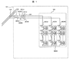
図1は、本発明の第1の実施形態を表した回路図である。まず、図1を用いて、本発明の電力変換器システム101の構成を説明する。
FIG. 1 is a circuit diagram showing a first embodiment of the present invention. First, the structure of the
本発明の電力変換器システム101は、電力変換器105,アームリアクトル201(201U〜201W),遮断機202,セル初充電回路252で構成される。アームリアクトル201は連系インピーダンスとして機能し、連系トランスで代用しても良い。
The
電力変換器105は3個のカスケードアーム113(113U〜113W)で構成される。
The
カスケードアーム113は、単位セル120がカスケードに接続された構造であり、該単位セル120は、図3のようなフルブリッジ120Fで構成される。該単位セル120は図4のようなチョッパ120Cでも構成してもよいが、フルブリッジ120Fの方が正負電圧を出力でき、制御性が高いので、以下、フルブリッジ回路120Fを単位セル120に用いた構成を例にとり説明する。
The cascade arm 113 has a structure in which the
該フルブリッジ回路120FはIGBTレッグ411(411L,411R)を2並列にして、直流コンデンサ406と接続した構成である。各IGBTレッグ411は、IGBT並列体402(402P,402N)を直列に接続した構成である。IGBT並列体402PとIGBT並列体402Nの接続部に入出力端子400(400L,400R)を設け、原則、各単位セルの入出力端子400同士がカスケード接続される。
The
より、詳細に記載すると、カスケードアーム113(113U,113V,113W)の両端の端子(602U〜W,603U〜W)以外の各単位セル120の出力端子400Nは他の単位セルの出力端子400Pに、各単位セルの出力端子400Pは他の単位セルの出力端子400Nに接続される。
More specifically, the
各カスケードアーム113(113U,113V,113W)の一方の端子602(602U〜602W)は該接続点600N互いにスター接続される。各カスケードアーム113(113U,113V,113W)の他方の端子603(603U〜603W)はそれぞれ、アームリアクトル201(201U,201V,201P)と電気的に接続される。
One terminal 602 (602U to 602W) of each cascade arm 113 (113U, 113V, 113W) is star-connected to the
また、アームリアクトル201(201U,201V,201P)は三相電力系統100などの交流電圧源に接続される。アームリアクトル201と三相電力系統100との接続点のことを連系点650(650U,650V,650W)と呼ぶ。
The arm reactor 201 (201U, 201V, 201P) is connected to an AC voltage source such as the three-
次に、本発明の電力変換器システム101の動作について説明する。
Next, the operation of the
まず、電力変換器システム101を構成する電力変換器105の各相の出力電圧について説明する。但し、特に断らない限り、電力変換器システム101の接続点600Nを基準電位とする。連系点650(650U,650V,650W)の電位を電力変換器105の各相出力電圧と定義する。
First, the output voltage of each phase of the
また、接続点603(603U,603V,603W)の電位を内側カスケード電圧V113(V113U,V113V,V113W)と定義する。 Further, the potential of the connection point 603 (603U, 603V, 603W) is defined as the inner cascade voltage V113 (V113U, V113V, V113W).
本発明の電力変換器システム101の通常動作を説明する。
The normal operation of the
本電力変換器システム101と三相電力系統100間の融通電力は、該電力変換システムの内側カスケード電圧の振幅と位相を系統電圧を基準に調整することにより制御できる。
The interchange power between the
一方、内側カスケード電圧は次のように制御できる。 On the other hand, the inner cascade voltage can be controlled as follows.
電力変換器システム101の各カスケードアーム113U,113V,113Wの入出力端子間(600Nと603U間、600Nと603V間、600Nと603W間)に印加される電圧は、各カスケードアーム113U,113V,113Wを構成する各単位セル120の出力電圧の合成電圧である。したがって、内側カスケード電圧V113U,V113V,V113Wは各カスケードアームの各単位セル120の出力電圧により制御できる。
The voltage applied between the input / output terminals (between 600N and 603U, between 600N and 603V, and between 600N and 603W) of each
内側カスケード電圧V113U,V113V,V113Wは、電力変換器105の出力電圧に相当するので、内側カスケード電圧V113U,V113V,V113Wを制御することにより、三相電力系統100と本電力変換器システム101の間の電力融通量を制御できる。単位セル120の出力電圧は各IGBTレッグ411をPWM制御することにより制御するので、各単位セルの直流コンデンサ406を所定の電圧に制御する必要がある。
Since the inner cascade voltages V113U, V113V, and V113W correspond to the output voltage of the
図2に単位セルの直流コンデンサ電圧が一定であるときのPWMの搬送波881、所望の正弦波電圧指令値882,PWMパルス883とPWMパルス883の基本波成分884を示す。通常、電力変換システムは所定の制御周期で制御することから、搬送波と比較するPWM用の電圧指令値は前記所定の時間ごとに更新されて、離散的な電圧指令値となる。前記条件では、PWMパルスの基本波成分804の位相・振幅は電圧指令値882の位相・振幅と異なってしまう。
FIG. 2 shows a
カスケードマルチレベル電力変換器システム101は単位セル120の数が増えると、高調波抑制の観点からは搬送波周波数を小さくできるので、所望の正弦波電圧指令802とPWMパルス883の基本波成分884との位相・振幅のずれがより大きくなる。
Since the cascade multilevel
単位セル120への入出電力は単位セル120の直流コンデンサ406の充放電電力となるので、PWMパルス883の基本波成分884の位相や振幅がずれると直流コンデンサ406の直流電圧に大きく影響する。
Since the input / output power to / from the
次に、本発明のポイントについて説明する。搬送波881周波数と制御周期が固定であれば、PWMパルス883の基本波成分884と該電圧指令値882との振幅や位相のずれは、電圧指令値882の変調率と該電圧指令値882と搬送波881との位相差により決まる。そこで、電圧指令値の変調率と位相毎に、変調率と位相補正値をテーブルとして準備して、電力変換システムの運転時に補正する。
Next, the points of the present invention will be described. If the frequency of the
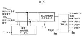
図5に本発明の電力変換システムの電圧指令値作成の主要ロジックを示す。 FIG. 5 shows the main logic for creating the voltage command value of the power conversion system of the present invention.
まず、図示されていない電流制御などで決まる単位セル電圧位相指令値701と単位セル電圧振幅指令値702を元に、位相・振幅偏差値テーブル711で、電圧位相補正値801,電圧位相補正値802を出力して、各単位セルの単位セル電圧位相指令値701と各単位セル電圧振幅指令値702に加算して、電圧指令値振幅値と電圧指令位相値を補正する。次に電圧指令波形作成ブロック715で電圧指令波形を合成して、PWMブロック721でPWMを行い単位セルの各IGBT451をオンオフ制御することにより、各単位セル120の出力電圧の基本波成分884は所望の電圧を出力できる。
First, based on a unit cell voltage
なお、図6のように、位相補正値テーブル712で修正後の位相,振幅値を直接出力したり、図示はしていないが、修正後の電圧指令を直接出力してもよい。 As shown in FIG. 6, the corrected phase and amplitude values may be directly output from the phase correction value table 712, or the corrected voltage command may be directly output although not shown.
以上により、各単位セル120は所定のPWMパルスの基本波成分884を出力できるので、各単位セル120の直流コンデンサ406の電圧アンバランスを抑制できる。
As described above, each
第1の実施例はテーブルを参照することにより、電圧指令値を補正したが、本実施例では、演算処理により電圧指令値を補正することを特徴とする。 In the first embodiment, the voltage command value is corrected by referring to the table. However, this embodiment is characterized in that the voltage command value is corrected by an arithmetic process.
具体的には、キャリア周期内で、正弦波電圧指令802とPWMパルス803の平均値が等しくなるようなPWM用の電圧指令値を演算するロジックを有することを特徴とする。 Specifically, it has a logic for calculating a voltage command value for PWM such that the average values of the sine wave voltage command 802 and the PWM pulse 803 are equal within the carrier period.
より具体的には、事前に電圧指令値の制御周期内の正弦波電圧指令802の平均値を演算して、その制御周期内では、該平均値をPWM電圧指令値とすればよい。 More specifically, an average value of the sine wave voltage command 802 within the control cycle of the voltage command value is calculated in advance, and the average value may be used as the PWM voltage command value within the control cycle.
図7は本実施例の電力変換システムの電圧指令値作成の主要ロジックを示す。 FIG. 7 shows the main logic for creating the voltage command value of the power conversion system of this embodiment.
まず、図示されていない電流制御などで決まる単位セル電圧位相指令値701と単位セル電圧振幅指令値702を元に、制御周期内電圧指令平均値演算ブロック719で各制御周期内での電圧指令値の平均値を演算して出力し、PWMブロック721で搬送波720と比較して、ゲートパルス740CP〜740DPを出力する。
各制御周期内でPWMパルス803と元の電圧指令値正弦波802が同じ電圧になるので、制御周波数が基本波周波数の整数倍であれば、PWMパルスの正弦波基本波成分804と正弦波電圧指令値802は大略等しくなり、各単位セル120の直流コンデンサ電圧のアンバランスの発生を抑制できる。
First, based on a unit cell voltage
Since the PWM pulse 803 and the original voltage command value sine wave 802 become the same voltage within each control period, if the control frequency is an integral multiple of the fundamental frequency, the sine wave fundamental wave component 804 of the PWM pulse and the sine wave voltage The command values 802 are substantially equal, and the occurrence of imbalance in the DC capacitor voltage of each
本発明は、無効電力補償装置(STATCOM)やBack−to−Backシステム(周波数変換装置など),直流送電システム(HVDC),モータドライブなどに利用可能である。 The present invention can be used for a reactive power compensator (STATCOM), a back-to-back system (frequency converter, etc.), a direct current power transmission system (HVDC), a motor drive, and the like.
100 三相電力系統
101 電力変換器システム
102 連系変圧器
102C 可変電圧変圧器
105 電力変換器
113Up,113Vp,113Wp,113Un,113Vn,113Wn カスケードレッグ
120 単位セル
121C 双方向チョッパ
121F フルブリッジ回路
201Up,201Vp,201Wp,201Un,201Vn,201Wn アームリアクトル
202 遮断機
250 可変直流電圧源
251 コンタクタ
252 初充電回路
400P,400N,400L,400R 単位セル出力端子
402P,402N IGBT並列体
406 直流コンデンサ
411,411L,411R IGBTレッグ
451 IGBT
452 ダイオード
600U カスケードレッグ113Upの高圧側端子
600V カスケードレッグ113Vpの高圧側端子
600W カスケードレッグ113Wpの高圧側端子
602U カスケードレッグ113Upの低圧側端子
602V カスケードレッグ113Vpの低圧側端子
602W カスケードレッグ113Wpの低圧側端子
603U カスケードレッグ113Unの高圧側端子
603V カスケードレッグ113Vnの高圧側端子
603W カスケードレッグ113Wnの高圧側端子
604U カスケードレッグ113Unの低圧側端子
604V カスケードレッグ113Vnの低圧側端子
604W カスケードレッグ113Wnの低圧側端子
650U,650V,650W 電力変換器105のU相入出力端子
701 単位セル電圧位相指令値
702 単位セル電圧振幅指令値
719 制御周期内電圧指令値平均値演算ブロック
720 搬送波
721 PWMブロック
740CP,740CN,740DP,740DN ゲートパルス出力
100 three-
452 Diode 600U High voltage side terminal 600V of cascade leg 113Up High voltage side terminal 600W of cascade leg 113Vp High voltage side terminal 602U of cascade leg 113Wp Low voltage side terminal 602V of cascade leg 113Up Low voltage side terminal 602W of cascade leg 113Vp Low voltage side terminal of
Claims (1)
Priority Applications (1)
| Application Number | Priority Date | Filing Date | Title |
|---|---|---|---|
| JP2010090016A JP5624792B2 (en) | 2010-04-09 | 2010-04-09 | Power converter |
Applications Claiming Priority (1)
| Application Number | Priority Date | Filing Date | Title |
|---|---|---|---|
| JP2010090016A JP5624792B2 (en) | 2010-04-09 | 2010-04-09 | Power converter |
Publications (3)
| Publication Number | Publication Date |
|---|---|
| JP2011223734A JP2011223734A (en) | 2011-11-04 |
| JP2011223734A5 JP2011223734A5 (en) | 2013-05-16 |
| JP5624792B2 true JP5624792B2 (en) | 2014-11-12 |
Family
ID=45039954
Family Applications (1)
| Application Number | Title | Priority Date | Filing Date |
|---|---|---|---|
| JP2010090016A Active JP5624792B2 (en) | 2010-04-09 | 2010-04-09 | Power converter |
Country Status (1)
| Country | Link |
|---|---|
| JP (1) | JP5624792B2 (en) |
Families Citing this family (14)
| Publication number | Priority date | Publication date | Assignee | Title |
|---|---|---|---|---|
| JP5752580B2 (en) * | 2011-12-12 | 2015-07-22 | 株式会社東芝 | Power converter |
| JP5938108B2 (en) * | 2012-01-11 | 2016-06-22 | ボンバルディール・トランスポーテイション・ゲゼルシヤフト・ミット・ベシュレンクテル・ハフツング | Generation of switching sequence of cascaded multi-level converter |
| CN102664418B (en) * | 2012-04-19 | 2014-07-02 | 威凡智能电气高科技有限公司 | PLC (programmable logic controller)-based on-line monitoring method in STATCOM (static synchronous compensator) |
| KR101791290B1 (en) * | 2013-07-02 | 2017-11-20 | 엘에스산전 주식회사 | Multi-level medium voltage inverter |
| CN104065062B (en) * | 2014-06-23 | 2016-08-24 | 许继电气股份有限公司 | The properly functioning modulation control method of STATCOM |
| JP2016067124A (en) * | 2014-09-25 | 2016-04-28 | 株式会社日立製作所 | Power compensator and power compensation method |
| JP6614704B2 (en) * | 2016-12-06 | 2019-12-04 | 東芝三菱電機産業システム株式会社 | Power converter |
| JP6704864B2 (en) * | 2017-01-16 | 2020-06-03 | 株式会社日立製作所 | Power converter |
| JP6892812B2 (en) * | 2017-10-12 | 2021-06-23 | 株式会社日立製作所 | Power converter |
| WO2020108736A1 (en) | 2018-11-27 | 2020-06-04 | Abb Schweiz Ag | Statcom arrangement without phase reactors |
| WO2020111513A1 (en) * | 2018-11-29 | 2020-06-04 | 중앙제어 주식회사 | Device for converting three-phase power regardless of direction of upward rotation |
| JP7375553B2 (en) | 2020-01-06 | 2023-11-08 | 富士電機株式会社 | power converter |
| JP7305594B2 (en) * | 2020-04-06 | 2023-07-10 | 東芝キヤリア株式会社 | power converter |
| KR102549613B1 (en) * | 2021-01-28 | 2023-06-29 | 부경대학교 산학협력단 | Devices and Method for Controlling the DC-link Voltage Balancing for Modular Converters |
Family Cites Families (3)
| Publication number | Priority date | Publication date | Assignee | Title |
|---|---|---|---|---|
| JPH0928083A (en) * | 1995-07-11 | 1997-01-28 | Hitachi Ltd | Pulse width modulation controller |
| JP2000287453A (en) * | 1999-03-31 | 2000-10-13 | Mitsubishi Electric Corp | Multiplex power converter |
| CN101427455B (en) * | 2006-06-16 | 2012-05-30 | 三菱电机株式会社 | Power converter control device |
-
2010
- 2010-04-09 JP JP2010090016A patent/JP5624792B2/en active Active
Also Published As
| Publication number | Publication date |
|---|---|
| JP2011223734A (en) | 2011-11-04 |
Similar Documents
| Publication | Publication Date | Title |
|---|---|---|
| JP5624792B2 (en) | Power converter | |
| US10263535B2 (en) | Method and device for voltage balancing of DC bus capacitors of neutral-point clamped four-level inverter | |
| JP4969614B2 (en) | Power converter | |
| Moosavi et al. | A voltage balancing strategy with extended operating region for cascaded H-bridge converters | |
| Sandeep et al. | Design and implementation of active neutral-point-clamped nine-level reduced device count inverter: an application to grid integrated renewable energy sources | |
| US10734884B2 (en) | Modular multilevel converter harmonic injection systems and methods | |
| US10236793B2 (en) | Grid connection power conversion device and output current control method thereof | |
| JP6289675B2 (en) | Power converter | |
| JP6178433B2 (en) | Power converter | |
| JP6538544B2 (en) | Self-excited reactive power compensator | |
| JP2009201248A (en) | Clamp power conversion apparatus | |
| JP6538542B2 (en) | Self-excited reactive power compensator | |
| CN111030497B (en) | Three-phase four-leg inverter parallel system, control method thereof and electric energy management equipment | |
| JP2016063687A (en) | Power conversion system | |
| CN111133670A (en) | Controlling a voltage source converter in a DC system | |
| Zhang et al. | DC-link capacitor voltage balancing for a five-level diode-clamped active power filter using redundant vectors | |
| Mei et al. | Quasi-fixed-frequency hysteresis current tracking control strategy for modular multilevel converters | |
| Bashi et al. | Generation of triggering signals for multilevel converter | |
| EP4220931A1 (en) | Power conversion device | |
| Kitidet et al. | A CB-SVPWM control strategy for neutral-poin voltage balancing in three-level NPC inverters | |
| JP2015015778A (en) | Power conversion system for system interconnection | |
| Shen et al. | Investigation of capacitor voltage regulation in modular multilevel converters with staircase modulation | |
| JP2017153277A (en) | Self-excited reactive power compensation apparatus | |
| JP5277096B2 (en) | Power converter | |
| KR101728019B1 (en) | Apparatus and method for controlling voltage of three-phase inverter for stand-alone microgrid |
Legal Events
| Date | Code | Title | Description |
|---|---|---|---|
| A621 | Written request for application examination |
Free format text: JAPANESE INTERMEDIATE CODE: A621 Effective date: 20130212 |
|
| A521 | Request for written amendment filed |
Free format text: JAPANESE INTERMEDIATE CODE: A523 Effective date: 20130329 |
|
| A977 | Report on retrieval |
Free format text: JAPANESE INTERMEDIATE CODE: A971007 Effective date: 20131128 |
|
| A131 | Notification of reasons for refusal |
Free format text: JAPANESE INTERMEDIATE CODE: A131 Effective date: 20131224 |
|
| A521 | Request for written amendment filed |
Free format text: JAPANESE INTERMEDIATE CODE: A523 Effective date: 20140220 |
|
| TRDD | Decision of grant or rejection written | ||
| A01 | Written decision to grant a patent or to grant a registration (utility model) |
Free format text: JAPANESE INTERMEDIATE CODE: A01 Effective date: 20140902 |
|
| A61 | First payment of annual fees (during grant procedure) |
Free format text: JAPANESE INTERMEDIATE CODE: A61 Effective date: 20140929 |
|
| R151 | Written notification of patent or utility model registration |
Ref document number: 5624792 Country of ref document: JP Free format text: JAPANESE INTERMEDIATE CODE: R151 |