JP5590106B2 - Matrix converter - Google Patents
Matrix converter Download PDFInfo
- Publication number
- JP5590106B2 JP5590106B2 JP2012269528A JP2012269528A JP5590106B2 JP 5590106 B2 JP5590106 B2 JP 5590106B2 JP 2012269528 A JP2012269528 A JP 2012269528A JP 2012269528 A JP2012269528 A JP 2012269528A JP 5590106 B2 JP5590106 B2 JP 5590106B2
- Authority
- JP
- Japan
- Prior art keywords
- phase
- generator
- switch drive
- drive signal
- current
- Prior art date
- Legal status (The legal status is an assumption and is not a legal conclusion. Google has not performed a legal analysis and makes no representation as to the accuracy of the status listed.)
- Expired - Fee Related
Links
Images


Description
開示の実施形態は、マトリクスコンバータに関する。 The disclosed embodiments relate to a matrix converter.
マトリクスコンバータは、高調波電流の抑制や回生電力の有効利用が可能であることから、新しい電力変換装置として注目されている。かかるマトリクスコンバータには、交流電源の各相と回転電機の各相とを接続する複数の双方向スイッチを備え、これらの双方向スイッチを制御して電力変換を行うものがある。 Matrix converters are attracting attention as new power converters because they can suppress harmonic currents and effectively use regenerative power. Such matrix converters include a plurality of bidirectional switches that connect each phase of the AC power source and each phase of the rotating electrical machine, and perform power conversion by controlling these bidirectional switches.
この種のマトリクスコンバータにおいて、交流電源が何らかの理由により低電圧となった場合に、電力変換動作を停止する技術が知られている。例えば、双方向スイッチによって交流電源の各相電圧を制御して発動機を駆動している状態で、交流電源が低電圧となった場合に、発動機への電力供給を停止させる技術がある(例えば、特許文献1参照)。 In this type of matrix converter, a technique is known in which the power conversion operation is stopped when the AC power supply becomes a low voltage for some reason. For example, there is a technique for stopping power supply to the motor when the AC power source becomes a low voltage while the motor is driven by controlling each phase voltage of the AC power source with a bidirectional switch ( For example, see Patent Document 1).
しかしながら、回転電機を負荷とするマトリクスコンバータにおいては、交流電源が低電圧になった場合でも、電力変換動作を停止させずに継続させることが望ましい。 However, in a matrix converter having a rotating electrical machine as a load, it is desirable to continue the power conversion operation without stopping even when the AC power supply becomes a low voltage.
実施形態の一態様は、上記に鑑みてなされたものであって、交流電源が低電圧になった場合でも、電力変換動作を継続することができるマトリクスコンバータを提供することを目的とする。 One aspect of the embodiments has been made in view of the above, and an object of the present invention is to provide a matrix converter capable of continuing the power conversion operation even when the AC power supply becomes a low voltage.
実施形態の一態様に係るマトリクスコンバータは、複数の双方向スイッチと、制御部とを備える。複数の双方向スイッチは、交流電源の各相と回転電機の各相とを接続する。制御部は、前記複数の双方向スイッチを制御して前記交流電源と前記回転電機との間の電力変換制御を行う。さらに、前記制御部は、前記双方向スイッチを構成する複数の片方向スイッチング素子のそれぞれを個別に120°通電制御およびPWM制御を併用してオン/オフ制御する。 A matrix converter according to an aspect of the embodiment includes a plurality of bidirectional switches and a control unit. The plurality of bidirectional switches connect each phase of the AC power source and each phase of the rotating electrical machine. The control unit controls the plurality of bidirectional switches to perform power conversion control between the AC power supply and the rotating electrical machine. Further, the control unit individually controls on / off of each of the plurality of unidirectional switching elements constituting the bidirectional switch using 120 ° energization control and PWM control individually.
実施形態の一態様によれば、交流電源が低電圧になった場合でも、電力変換動作を継続することができるマトリクスコンバータを提供することができる。 According to one aspect of the embodiment, it is possible to provide a matrix converter that can continue the power conversion operation even when the AC power supply becomes a low voltage.
以下、添付図面を参照して、本願の開示するマトリクスコンバータの実施形態を詳細に説明する。なお、以下に示す実施形態によりこの発明が限定されるものではない。 Hereinafter, embodiments of a matrix converter disclosed in the present application will be described in detail with reference to the accompanying drawings. In addition, this invention is not limited by embodiment shown below.
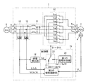
図1は、実施形態に係るマトリクスコンバータの構成例を示す図である。以下の実施形態では、交流発電機(ACG)である回転電機の発電電力を変換して交流電源へ供給するマトリクスコンバータを例に挙げて説明するが、回転電機は交流発電機に限らず、例えば、交流電動機としてもよい。また、交流電源として電力系統(Grid)を例に挙げて説明するが、交流電源はこれに限られない。 FIG. 1 is a diagram illustrating a configuration example of a matrix converter according to the embodiment. In the following embodiments, a matrix converter that converts the generated electric power of a rotating electrical machine that is an AC generator (ACG) and supplies it to an AC power source will be described as an example. However, the rotating electrical machine is not limited to an AC generator, An AC motor may be used. Moreover, although an electric power system | strain (Grid) is mentioned as an example and demonstrated as an alternating current power supply, an alternating current power supply is not restricted to this.
図1に示すように、実施形態に係るマトリクスコンバータ1は、3相交流の電力系統2と回転電機3との間に設けられ、電力系統2と回転電機3との間の電力変換を行う。なお、以下においては、回転電機3の一例として、同期発電機を用いた場合の例を説明する。
As shown in FIG. 1, a matrix converter 1 according to the embodiment is provided between a three-phase
回転電機3の回転軸には、回転電機3の回転位置を検出する位置検出器4が設けられており、かかる位置検出器4によって検出された回転電機3の回転位置θGはマトリクスコンバータ1へ入力される。
A
マトリクスコンバータ1は、電力変換部10と、LCフィルタ11と、電流検出部12と、電圧検出部13と、停電検出部14と、制御部15とを備える。また、マトリクスコンバータ1は、系統側端子Tr、Ts、Ttおよび発電機側端子Tu、Tv、Twを備え、系統側端子Tr、Ts、Ttに電力系統2が接続され、発電機側端子Tu、Tv、Twに回転電機3が接続される。
The matrix converter 1 includes a
電力変換部10は、電力系統2のR相、S相およびT相の各相と回転電機3のU相、V相およびW相の各相とを接続する複数の双方向スイッチSw1〜Sw9を備える。双方向スイッチSw1〜Sw3は、電力系統2のR相、S相、T相と回転電機3のU相とをそれぞれ接続する双方向スイッチである。双方向スイッチSw4〜Sw6は、電力系統2のR相、S相およびT相と回転電機3のV相とをそれぞれ接続する双方向スイッチである。双方向スイッチSw7〜Sw9は、電力系統2のR相、S相およびT相と回転電機3のW相とをそれぞれ接続する双方向スイッチである。
The
双方向スイッチSw1〜Sw9は、例えば、図2に示すような構成を有する。図2は、各双方向スイッチSw1〜Sw9の構成例を示す図である。図2に示すように、各双方向スイッチSw1〜Sw9は、片方向スイッチング素子31とダイオード33とによる直列接続体と、片方向スイッチング素子32とダイオード34とによる直列接続体とが、逆方向に並列に接続されて構成される。
The bidirectional switches Sw1 to Sw9 have a configuration as shown in FIG. 2, for example. FIG. 2 is a diagram illustrating a configuration example of each of the bidirectional switches Sw1 to Sw9. As shown in FIG. 2, each of the bidirectional switches Sw <b> 1 to Sw <b> 9 includes a series connection body composed of a
片方向スイッチング素子31、32は、例えば、IGBT(Insulated Gate Bipolar Transistor)などの半導体素子が用いられる。双方向スイッチSw1〜Sw9を構成する片方向スイッチング素子31、32を個別にオン/オフすることで、通電方向を制御することができる。
As the
なお、双方向スイッチSw1〜Sw9は、図2に示す構成に限られない。例えば、双方向スイッチSw1〜Sw9は、片方向スイッチング素子31、32をそれぞれ逆阻止型のスイッチング素子とし、これらのスイッチング素子を互いに逆方向に並列接続した構成でもよく、また、後述する図12に示す構成であってもよい。
Note that the bidirectional switches Sw1 to Sw9 are not limited to the configuration shown in FIG. For example, the bidirectional switches Sw1 to Sw9 may be configured such that the
LCフィルタ11は、電力系統2のR相、S相およびT相と電力変換部10との間に設けられ、電力変換部10から電力系統2へのノイズの影響を抑制する。具体的には、LCフィルタ11は、3つのリアクトルと3つのコンデンサによって構成され、電力変換部10を構成する双方向スイッチSw1〜Sw9のスイッチングに起因する高周波成分(PWM成分)を除去する。これにより、電力変換部10によって発生する高周波成分の電力系統2への出力を抑制することができる。なお、LCフィルタ11は、図1に示す構成に限られず、例えば、リアクトルを設けない構成でもよい。
The LC filter 11 is provided between the R phase, S phase, and T phase of the
なお、3つのリアクトルの一端は、電力系統2のR相、S相およびT相側と電力変換部10との間の電力系統2側に接続され、3つのリアクトルの他端は、電力変換部10側に接続される。また、3つコンデンサは、異なる2つのリアクトルの他端間に接続される。
Note that one end of each of the three reactors is connected to the
電流検出部12は、電力系統2とLCフィルタ11との間に設けられ、電力系統2のR相、S相、T相の各相とLCフィルタ11との間に流れる電流の電流値Ir、Is、It(以下、「系統相電流値Ir、Is、It」と記載する)を検出する。なお、電流検出部12は、例えば、磁電変換素子であるホール素子を利用して電流を検出する電流センサである。
The
電圧検出部13は、電力系統2と電力変換部10との間に設けられ、電力系統2のR相、S相、T相の各相の電圧値Vr、Vs、Vt(以下、「系統相電圧値Vr、Vs、Vt」と記載する)を検出する。
The
停電検出部14は、系統電圧の電圧値Va(以下、系統電圧値Vaと記載する)が電圧値V1以下であるか否かを検出する。停電検出部14は、系統電圧値Vaが電圧値V1以下である場合には、電力系統2が停電したと判定してHighレベルの停電検出信号Sdを出力する。一方、停電検出部14は、系統電圧値Vaが電圧値V1を超える場合には、電力系統2が停電していないと判定してLowレベルの停電検出信号Sdを出力する。
The power
停電検出部14は、系統相電圧値Vr、Vs、Vtを固定座標上の直交した2軸のαβ成分へ変換して、α軸方向の系統電圧値Vαとβ軸方向の系統電圧値Vβとを求める。そして、停電検出部14は、系統電圧値Vα、Vβの自乗和平方根(=√(Vα 2+Vβ 2))を演算し、演算結果を系統電圧値Vaとする。
The power
制御部15は、第1の駆動制御部20と、第2の駆動制御部21と、切替部22とを備える。第1の駆動制御部20は、回転電機3の発生するトルク量を指示するトルク指令に基づいて電圧指令を生成し、公知のマトリクスコンバータのPWM制御方法によって電圧指令に応じた電圧を回転電機3に出力するためのスイッチ駆動信号S1〜S18を生成して電力変換部10へ出力する。
The
なお、電圧指令は、トルク指令に基づいて公知の同期発電機のベクトル制御則によって生成される。また、スイッチ駆動信号S1〜S18によって、電力変換部10は、複数の双方向スイッチSw1〜Sw9をそれぞれ構成する複数の片方向スイッチング素子31、32を共にオンにしつつ、電圧指令に応じた電圧をPWM制御により出力し、流れる電流の大きさや通電方向が出力電圧と発電電圧の関係で決まる電力変換を行う。
The voltage command is generated based on a known vector control law of a synchronous generator based on the torque command. In addition, the
第2の駆動制御部21は、系統相電圧値Vr、Vs、Vtおよび系統相電流値Ir、Is、Itに基づいて、複数の双方向スイッチSw1〜Sw9をそれぞれ構成する複数の片方向スイッチング素子31、32の一部をオンにして電力変換制御を行う。
The second
複数の双方向スイッチSw1〜Sw9をそれぞれ構成する複数の片方向スイッチング素子31、32の一部をオンにすることで、通電方向を制御することができる。これにより、電力系統2の電圧が回転電機3の電圧よりも極端に低い停電のような場合であっても、回転電機3と電力系統2の間に大電流が流れ続けることを避け、電流制御を行いつつ電力変換動作を行うことができる。
The energization direction can be controlled by turning on some of the plurality of
例えば、第2の駆動制御部21は、複数の双方向スイッチSw1〜Sw9を構成する片方向スイッチング素子31、32のうち、電力系統2側のいずれか2つの相の間に電流を流す片方向スイッチング素子を常にオンにする。また、第2の駆動制御部21は、複数の双方向スイッチSw1〜Sw9を構成する片方向スイッチング素子31、32のうち、回転電機3側のいずれか2つの相の間に電流を流す片方向スイッチング素子を常にオンにする。かかる制御によって、電力系統2のどれか2つの相の間および回転電機3のどれか2つの相の間に電流を流し続けることができる。
For example, the second
かかる制御において、第2の駆動制御部21は、双方向スイッチSw1〜Sw9を構成する複数の片方向スイッチング素子31、32のそれぞれを個別に120°通電制御およびPWM制御を併用してオン/オフ制御することで共振現象の発生を抑制する。なお、かかる点の詳細については、図6〜図10を参照して後述する。
In such control, the second
切替部22は、停電検出部14から出力される停電検出信号Sdに基づいて、電力変換部10へ出力するスイッチ駆動信号S1〜S18を選択して出力する。具体的には、切替部22は、停電検出部14から出力される停電検出信号SdがLowレベルである場合、第1の駆動制御部20によって生成されるスイッチ駆動信号Sa1〜Sa18をスイッチ駆動信号S1〜S18として出力する。
Based on the power failure detection signal Sd output from the power
一方、切替部22は、停電検出部14から出力される停電検出信号SdがHighレベルである場合、第2の駆動制御部21によって生成されるスイッチ駆動信号Sb1〜Sb18をスイッチ駆動信号S1〜S18として出力する。
On the other hand, when the power failure detection signal Sd output from the power
したがって、電力系統2が低電圧になった場合に、第2の駆動制御部21によって生成されるスイッチ駆動信号Sb1〜Sb18によって、双方向スイッチSw1〜Sw9をそれぞれ構成する複数の片方向スイッチング素子31、32の一部をオンにする電力変換制御を行う。これにより、電力系統2が低電圧になった場合でも、電力変換動作を継続することができる。
Therefore, when the
このように、制御部15は、双方向スイッチSw1〜Sw9を構成する複数の片方向スイッチング素子31、32を共に制御して電力変換制御を行う第1の制御モードと、双方向スイッチSw1〜Sw9を構成する複数の片方向スイッチング素子31、32の一部を個別に制御して電力変換制御を行う第2の制御モードとを切り替えて実行する。
As described above, the
具体的には、制御部15では、交流電源の電圧である系統電圧値Vaが所定値である電圧値V1を超える場合に、第1の駆動制御部20が第1の制御モードを実行する。一方、系統電圧値Vaが電圧値V1以下である場合に、第2の駆動制御部21が第2の制御モードを実行する。
Specifically, in the
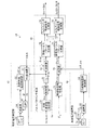
以下、第2の駆動制御部21の具体的構成の一例について具体的に説明する。図3は、第2の駆動制御部21の具体的構成の一例を示す図である。図3に示すように、第2の駆動制御部21は、有効電流補償部41と、無効電流補償部42と、パルスパターン生成部43とを備える。
Hereinafter, an example of a specific configuration of the second
まず、有効電流補償部41について説明する。有効電流補償部41は、PQ変換器51と、ローパスフィルタ(LPF)52と、系統有効電流指令器53と、減算器54と、系統有効電流制御器55とを備える。かかる有効電流補償部41は、系統有効電流値が系統有効電流指令IPrefと一致するように、系統位相補償値dθrstを生成し、生成した系統位相補償値dθrstをパルスパターン生成部43へ出力する。
First, the active
PQ変換器51は、系統相電流値Ir、Is、Itを固定座標上の直交した2軸のαβ成分へ変換して、α軸方向の系統電流値Iαとβ軸方向の系統電流値Iβとを求める。さらに、PQ変換器51は、αβ軸座標系の成分を、電力系統2の電圧位相θrst(以下、「系統位相θrst」と記載する)に応じて回転する回転座標系の成分へ変換することによって、系統有効電流IPと系統無効電流IQとを求める。
The
PQ変換器51は、例えば、下記式(1)の演算を行うことで、系統有効電流IPと系統無効電流IQとを求める。

LPF52は、系統有効電流IPから高周波成分を除去して減算器54へ出力する。これにより、系統有効電流IPから高周波成分による影響を除去するようにしている。
The
減算器54は、系統有効電流指令器53から出力される系統有効電流指令IPrefからLPF52の出力を減算することによって、系統有効電流指令IPrefと系統有効電流IPとの偏差である系統有効電流偏差を演算し、系統有効電流制御器55へ出力する。
The
系統有効電流制御器55は、例えば、PI(比例積分)制御器から構成され、系統有効電流偏差がゼロとなるように比例積分演算を行うことによって、系統位相補償値dθrstを生成する。ここでは、系統有効電流指令IPrefは、ゼロに設定されており、系統有効電流制御器55は、系統有効電流IPがゼロとなるように系統位相補償値dθrstを生成する。
The grid active
次に、無効電流補償部42について説明する。無効電流補償部42は、ローパスフィルタ(LPF)61と、系統無効電流指令器62と、減算器63と、系統無効電流制御器64とを備える。かかる無効電流補償部42は、系統無効電流値が系統無効電流指令IQrefと一致するように、発電機位相補正値dθuvwを生成し、生成した発電機位相補正値dθuvwをパルスパターン生成部43へ出力する。
Next, the reactive
減算器63は、系統無効電流指令器62から出力される系統無効電流指令IQrefからLPF61の出力を減算することによって、系統無効電流指令IQrefと系統無効電流IQとの偏差である系統無効電流偏差を演算し、系統無効電流制御器64へ出力する。
The
系統無効電流制御器64は、例えば、PI制御器から構成され、系統無効電流偏差がゼロとなるように比例積分演算を行うことによって、発電機位相補正値dθuvwを生成する。系統無効電流指令IQrefは、例えば、系統電圧値Vaに応じた値とすることができる。 The grid reactive current controller 64 is constituted by, for example, a PI controller, and generates a generator phase correction value dθuvw by performing a proportional-integral calculation so that the grid reactive current deviation becomes zero. The system reactive current command IQref can be set to a value corresponding to the system voltage value Va, for example.
図4は、系統無効電流指令IQrefと系統電圧値Vaとの関係の一例を示す図である。図4に示すように、系統無効電流指令器62は、系統電圧値Vaが第2閾値である電圧値V2を超え、かつ第1閾値である電圧値V1以下の領域では、系統電圧値Vaの増加に伴い直線的に減少する系統無効電流指令IQrefを生成する。
FIG. 4 is a diagram illustrating an example of the relationship between the grid reactive current command IQref and the grid voltage value Va. As shown in FIG. 4, the grid reactive
また、系統無効電流指令器62は、系統電圧値Vaが第2閾値である電圧値V2以下の場合に、最大値となり、第1閾値である電圧値V1を超える領域では、ゼロ値となる系統無効電流指令IQrefを生成する。なお、系統無効電流指令IQrefと系統電圧値Vaとの関係は、図4に示す例に限定するものではなく、異なる関係であってもよい。
In addition, the system reactive
次に、図3に示すパルスパターン生成部43について説明する。パルスパターン生成部43は、系統相電圧値Vr、Vs、Vt、回転位置θG、系統位相補償値dθrst、発電機位相補正値dθuvw、停電検出信号Sdに基づき、双方向スイッチSw1〜Sw9を駆動するスイッチ駆動信号S1〜S18を生成する。
Next, the pulse
パルスパターン生成部43は、系統周波数検出器70と、保持器71と、積分器72と、加算器73と、発電機位相生成器74と、加算器75とを備える。また、パルスパターン生成部43は、系統パルスパターン生成器76と、発電機パルスパターン生成器77と、GeGrスイッチ駆動信号生成器78と、GrGeスイッチ駆動信号生成器79とを備える。
The pulse
系統周波数検出器70は、例えば、PLL(Phase Locked Loop)であり、系統相電圧値Vr、Vs、Vtに基づき、電力系統2の電圧周波数と同期した系統周波数frstを出力する。
The system frequency detector 70 is, for example, a PLL (Phase Locked Loop), and outputs a system frequency frst synchronized with the voltage frequency of the
保持器71は、停電検出信号SdがLowレベルからHighレベルに変化したタイミングで、系統周波数検出器70から出力される系統周波数frstを保持し、HighレベルからLowレベルに変化したタイミングで、系統周波数frstの保持を解除する。
The
積分器72は、保持器71から出力される系統周波数frstを積分し、系統位相θrstを生成し、有効電流補償部41および加算器73へ出力する。加算器73は、系統位相θrstに系統位相補償値dθrstを加算して系統補正位相θrst’を生成し、生成した系統補正位相θrst’を系統パルスパターン生成器76へ出力する。
The integrator 72 integrates the system frequency frst output from the
発電機位相生成器74は、回転位置θGに回転電機3の極対数を掛け算することにより、発電機位相θuvwを生成し、加算器75へ出力する。加算器75は、発電機位相θuvwに発電機位相補正値dθuvwを加算して発電機補正位相θuvw’を生成し、生成した発電機補正位相θuvw’を発電機パルスパターン生成器77へ出力する。
Generator phase generator 74, by multiplying the number of pole pairs of the rotary electric machine 3 to the rotational position theta G, generates a generator phase Shitauvw, and outputs it to the
パルスパターン生成部43は、図5に示す電流形インバータモデルを用いてスイッチ駆動信号S1〜S18を生成する。図5は、電流形インバータモデルを示す図である。
The pulse
図5に示す電流形インバータモデル80は、コンバータ81とインバータ82を備えるモデルである。コンバータ81は、電力系統2のR相、S相、T相にフルブリッジ接続された複数のスイッチング素子から構成される。かかるコンバータ81の各スイッチング素子は、スイッチ駆動信号Srp、Ssp、Stp、Srn、Ssn、Stn(以下、「スイッチ駆動信号Srp〜Stn」と記載する)によって駆動される。
A current
インバータ82は、回転電機3のU相、V相、W相にフルブリッジ接続された複数のスイッチング素子から構成される。かかるインバータ82の各スイッチング素子は、スイッチ駆動信号Sup、Svp、Swp、Sun、Svn、Swn(以下、「スイッチ駆動信号Sup〜Swn」と記載する)によって駆動される。
The
系統パルスパターン生成器76は、系統位相θrstに対して120°通電の電流を流すコンバータ81のスイッチ駆動信号Srp〜Stnのパターンを有しており、系統補正位相θrst’に応じてスイッチ駆動信号Srp〜Stnを生成する。図6は、系統位相θrstとスイッチ駆動信号Srp〜Stnとの関係を示す図であり、系統位相θrstに対して90°進んだ120°通電の電流を流すための両者の関係を表すものである。
The system
系統補正位相θrst’は、系統有効電流IPがゼロとなるように求められた系統位相補償値dθrstが系統位相θrstに加算されて生成される。そのため、系統パルスパターン生成器76は、系統補正位相θrst’に基づき、図6に示すようにスイッチ駆動信号Srp〜Stnを生成することにより、電力系統2側に90°進みでかつ系統有効電流IPがゼロである無効電流を流すことができる。
The system correction phase θrst ′ is generated by adding the system phase compensation value dθrst obtained so that the system active current IP becomes zero to the system phase θrst. Therefore, the system
系統パルスパターン生成器76は、電力系統2側のいずれか2つの相の間に電流を流すスイッチング素子を常にオンにするようにスイッチ駆動信号Srp〜Stnを生成する。例えば、0°≦θrst<30°、330°≦θrst<360°の範囲にある場合、スイッチ駆動信号Stn、SspがHighレベルであり、その他はLowレベルである。これにより、T相とS相との間に電流が流れる。
The system
同様に、30°≦θrst<90°の範囲にある場合、スイッチ駆動信号Srn、SspがHighレベルであり、R相とS相との間に電流が流れる。90°≦θrst<150°の範囲にある場合、スイッチ駆動信号Srn、StpがHighレベルであり、R相とT相との間に電流が流れる。150°≦θrst<210°の範囲にある場合、スイッチ駆動信号Ssn、StpがHighレベルであり、S相とT相との間に電流が流れる。 Similarly, when it is in a range of 30 ° ≦ θrst <90 °, the switch drive signals Srn and Ssp are at a high level, and a current flows between the R phase and the S phase. In the case of 90 ° ≦ θrst <150 °, the switch drive signals Srn and Stp are at a high level, and a current flows between the R phase and the T phase. When it is in the range of 150 ° ≦ θrst <210 °, the switch drive signals Ssn and Stp are at the high level, and a current flows between the S phase and the T phase.
210°≦θrst<270°の範囲にある場合、スイッチ駆動信号Ssn、SrpがHighレベルであり、S相とR相との間に電流が流れる。270°≦θrst<330°の範囲にある場合、スイッチ駆動信号Stn、SrpがHighレベルであり、T相とR相との間に電流が流れる。このように、系統パルスパターン生成器76は、系統位相θrstに対して90°進んだ位相の電流が流れるようにパルスパターンを生成する。
When in the range of 210 ° ≦ θrst <270 °, the switch drive signals Ssn and Srp are at a high level, and a current flows between the S phase and the R phase. In the case of 270 ° ≦ θrst <330 °, the switch drive signals Stn and Srp are at a high level, and a current flows between the T phase and the R phase. Thus, the system
電力系統2側のいずれか2つの相の間に電圧波形から位相が90°進んだ電流を流すように、コンバータ81に対して120°通電制御を行った場合、流れる電流にLCフィルタ11の共振周波数と一致する周波数成分が含まれることがあり、これによって共振現象が発生する。かかる共振現象が発生した場合、電力系統2側のいずれか2つの相の間に流れる電流や電圧の波形に歪が生じる。
In the case where 120 ° energization control is performed on the
パルスパターン生成部43は、スイッチ駆動信号Srp〜Stnによって駆動される各スイッチング素子に対して、120°通電制御およびPWM制御を併用してオン/オフ制御を行うことによって共振現象の発生を抑制する。
The pulse
例えば、図6に示すように、パルスパターン生成部43の系統パルスパターン生成器76は、30°≦θrst<150°の範囲でスイッチ駆動信号SrnがHighレベルとなる120°通電制御用のパルスパターンを生成する。
For example, as shown in FIG. 6, the system
かかる場合、系統パルスパターン生成器76は、例えば、0°≦θrst<30°の範囲で、θrstが30°に近くなるほど、スイッチ駆動信号SrnがHighレベルとなるパルス幅が段階的に大きくなるPWM制御用のパルスパターンを生成する。また、系統パルスパターン生成器76は、150°≦θrst<180°の範囲で、θrstが180°に近くなるほど、スイッチ駆動信号SrnがHighレベルとなるパルスの幅が段階的に小さくなるPWM制御用のパルスパターンを生成する。
In such a case, the system
そして、系統パルスパターン生成器76は、他のスイッチ駆動信号Ssn、Stn、Srp、Ssp、Stpについても、図6に示すように、120°通電用のパルスパターンとPWM制御用のパルスパターンとを同様に生成する。
The system
そして、パルスパターン生成部43は、これらのスイッチ駆動信号Srp〜Stn、および後に詳述する発電機パルスパターン生成器77によって生成されるスイッチ駆動信号Sup〜Swnに基づいてスイッチ駆動信号S1〜S18を生成する。これにより、電力系統2側のいずれか2つの相の間に流す電流の波形を正弦波形に近付けることができるので、共振現象の発生を抑制することができる。
The pulse
ここで、図7および図8を参照し、スイッチ駆動信号Srp〜Stnを生成する系統パルスパターン生成器76の具体的構成の一例について説明する。図7は、系統パルスパターン生成器76の具体的構成の一例を示す図であり、図8は、系統パルスパターン生成器76の動作の一例を示す図である。
Here, an example of a specific configuration of the system
図7に示すように、系統パルスパターン生成器76は、タイマ91と、位相シフト器761、762と、R相用駆動信号生成器90aと、S相用駆動信号生成器90bと、T相用駆動信号生成器90cとを備える。
As shown in FIG. 7, the system
タイマ91は、停電検出信号SdがHighレベルになった時点からの時間を計測する。かかるタイマ91は、図示しないプロセッサの動作クロックに基づいて時間の計測を行い、計測した時間をR相用駆動信号生成器90aと、S相用駆動信号生成器90bと、T相用駆動信号生成器90cとへ出力する。
The timer 91 measures the time from when the power failure detection signal Sd becomes High level. The timer 91 measures time based on an operation clock of a processor (not shown), and uses the measured time for the R-phase drive signal generator 90a, the S-phase
位相シフト器761は、加算器73(図3参照)から入力される系統補正位相θrst’に120°の位相を加算してS相用駆動信号生成器90bへ出力する。また、位相シフト器762は、加算器73(図3参照)から入力される系統補正位相θrst’に240°の位相を加算してT相用駆動信号生成器90cへ出力する。なお、R相用駆動信号生成器90aには、加算器73(図3参照)から系統補正位相θrst’が入力される。
The
R相用駆動信号生成器90aは、電力系統2のR相へ流す電流を制御するためのスイッチ駆動信号Srp、Srnを生成してGeGrスイッチ駆動信号生成器78およびGrGeスイッチ駆動信号生成器79(図3参照)へ出力する。
The R-phase drive signal generator 90a generates switch drive signals Srp and Srn for controlling the current flowing to the R-phase of the
S相用駆動信号生成器90bは、電力系統2のS相へ流す電流を制御するためのスイッチ駆動信号Ssp、Ssnを生成してGeGrスイッチ駆動信号生成器78およびGrGeスイッチ駆動信号生成器79(図3参照)へ出力する。
The S-phase
T相用駆動信号生成器90cは、電力系統2のT相へ流す電流を制御するためのスイッチ駆動信号Stp、Stnを生成してGeGrスイッチ駆動信号生成器78およびGrGeスイッチ駆動信号生成器79(図3参照)へ出力する。
The T-phase
ここで、S相用駆動信号生成器90bは、スイッチ駆動信号Srnよりも120°位相が遅れたスイッチ駆動信号Ssn、スイッチ駆動信号Srpよりも120°位相が遅れたスイッチ駆動信号Sspを出力するが、R相用駆動信号生成器90aと同一構成である。
Here, the S-phase
また、T相用駆動信号生成器90cは、スイッチ駆動信号Srnよりも240°位相が遅れたスイッチ駆動信号Stn、スイッチ駆動信号Srpよりも240°位相が遅れたスイッチ駆動信号Stpを出力するが、R相用駆動信号生成器90aと同一構成である。
The T-phase
このため、ここでは、R相用駆動信号生成器90aの構成および動作について説明し、S相用駆動信号生成器90b、T相用駆動信号生成器90cが備える構成要素については、R相用駆動信号生成器90aと同一の符号を付することにより、その説明を省略する。
Therefore, here, the configuration and operation of the R-phase drive signal generator 90a will be described, and the components included in the S-phase
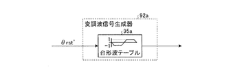
R相用駆動信号生成器90aは、変調波信号生成器92と、キャリア信号生成器93と、比較器94とを備える。また、変調波信号生成器92は、正弦波生成器95と増幅器96とを備える。正弦波生成器95は、加算器73(図3参照)から入力される系統補正位相θrst’と180°位相の異なる正弦波信号を生成し、増幅器96へ出力する。このとき、正弦波生成器95は、振幅が「‐1」と「1」との間で変動する正弦波信号を生成して増幅器96へ出力する。
The R-phase drive signal generator 90 a includes a modulated
増幅器96は、正弦波生成器95から入力される変調波信号の振幅を2倍に増幅することによって変調波信号(図8参照)を生成し、比較器94へ出力する。
The
キャリア信号生成器93は、三角波生成器97と増幅器98とを備える。三角波生成器97は、タイマ91から入力される時間と所定のキャリア周波数とに基づいて、図8に示すように、振幅が「0」と「1」との間で変動する三角波である第1のキャリア信号を生成し、比較器94と増幅器98とへ出力する。増幅器98は、図8に示すように、第1のキャリア信号を−1倍に増幅することによって振幅が「0」と「−1」との間で変動する三角波である第2のキャリア信号を生成し、比較器94へ出力する。
The
比較器94は、第1の比較器99と第2の比較器100とを備える。第1の比較器99の非反転入力には、変調波信号生成器92から変調波信号が入力され、反転入力には、キャリア信号生成器93から第1のキャリア信号が入力される。かかる第1の比較器99は、変調波信号と第1のキャリア信号とを逐次比較し、変調波信号の信号レベルが第1のキャリア信号の信号レベルよりも大きい位相の範囲でHighレベルとなるスイッチ駆動信号Srpを生成する。
The
そして、第1の比較器99は、生成したスイッチ駆動信号SrpをGeGrスイッチ駆動信号生成器78およびGrGeスイッチ駆動信号生成器79(図3参照)へ出力する。ここで、振幅が「0」と「1」との間で変動する第1キャリア信号と比較される変調波信号の波形は、振幅が「−1」と「1」との間で変動する正弦波信号の振幅を2倍に増幅した正弦波の波形である。したがって、スイッチ駆動信号Srpは、210°≦θrst<330°の範囲では、常にHighレベルとなり、120°通電制御用のパルスパターンになる。
Then, the
また、180°≦θrst<210°の範囲、および330°≦θrst<360°の範囲で、スイッチ駆動信号Srpは、変調波信号が第1のキャリア信号よりも大きな位相の範囲で断続的にHighレベルとなり、PWM制御用のパルスパターンになる。 In addition, in the range of 180 ° ≦ θrst <210 ° and the range of 330 ° ≦ θrst <360 °, the switch drive signal Srp is intermittently high in the range of the phase of the modulated wave signal larger than that of the first carrier signal. The level becomes a pulse pattern for PWM control.
一方、第2の比較器100の非反転入力には、キャリア信号生成器93から第2のキャリア信号が入力され、反転入力には、変調波信号生成器92から変調波信号が入力される。かかる第2の比較器100は、第2のキャリア信号と変調波信号とを逐次比較し、第2のキャリア信号の信号レベルが変調波信号の信号レベルよりも大きい位相の範囲でHighレベルとなるスイッチ駆動信号Srnを生成する。
On the other hand, the second carrier signal is input from the
そして、第2の比較器100は、生成したスイッチ駆動信号SrnをGeGrスイッチ駆動信号生成器78およびGrGeスイッチ駆動信号生成器79(図3参照)へ出力する。これにより、スイッチ駆動信号Srnは、30°≦θrst<150°の範囲では、常にHighレベルとなり、120°通電制御用のパルスパターンになる。
Then, the
また、0°≦θrst<30°の範囲、および150°≦θrst<180°の範囲で、スイッチ駆動信号Srnは、第2のキャリア信号が変調波信号よりも大きな位相の範囲で断続的にHighレベルとなり、PWM制御用のパルスパターンになる。 In addition, in the range of 0 ° ≦ θrst <30 ° and 150 ° ≦ θrst <180 °, the switch drive signal Srn is intermittently high in the range where the second carrier signal is larger in phase than the modulation wave signal. The level becomes a pulse pattern for PWM control.
このように、R相用駆動信号生成器90aは、120°通電制御を行うためのスイッチ駆動信号Srp、Srnと、120°通電制御を行う前後でPWM制御を行うためのスイッチ駆動信号Srp、Srnとを生成する。 As described above, the R-phase drive signal generator 90a includes the switch drive signals Srp and Srn for performing the 120 ° energization control, and the switch drive signals Srp and Srn for performing the PWM control before and after performing the 120 ° energization control. And generate
なお、図7に示すキャリア信号生成器93は、R相用駆動信号生成器90a、S相用駆動信号生成器90b、T相用駆動信号生成器90cのいずれか一つに設けられてもよい。例えば、R相用駆動信号生成器90aに選択的にキャリア信号生成器93を設けてもよい。かかる場合、R相用駆動信号生成器90aに設けられるキャリア信号生成器93によって、S相用駆動信号生成器90bおよびT相用駆動信号生成器90cの比較器94へ第1のキャリア信号と第2のキャリア信号とを供給する。
The
また、R相用駆動信号生成器90aの変調波信号生成器92から出力される変調波信号の位相を120°シフトさせた信号と、240°シフトさせた信号とをS相用駆動信号生成器90bおよびT相用駆動信号生成器90cの比較器94へそれぞれ供給してもよい。かかる構成とすれば、位相シフト器761、762を省略することができるとともに、S相用駆動信号生成器90bおよびT相用駆動信号生成器90cから変調波信号生成器92を省略することができる。
Also, an S-phase drive signal generator generates a signal obtained by shifting the phase of the modulated wave signal output from the modulated
また、図7に示す系統パルスパターン生成器76の構成は、一例であり、変調波信号生成器92の構成や、R相用駆動信号生成器90a、S相用駆動信号生成器90b、T相用駆動信号生成器90cの構成は、さらに種々の変形が可能である。図9は、変形例1に係る変調波信号生成器92aの構成を示す図であり、図10は、変形例2に係るR相用駆動信号生成器90dの構成を示す図である。
The configuration of the system
図9に示すように、変形例1に係る変調波信号生成器92aは、正弦波生成器95(図7参照)に代えて、台形波テーブル95aを備える。台形波テーブル95aは、120°通電制御を行う位相範囲で振幅が「1」または「−1」に固定され、120°通電制御を行う前後の位相範囲で直線となる台形波が記憶されたテーブルである。そして、台形波テーブル95aは、加算器73(図3参照)から入力される系統補正位相θrst’に応じた位相で台形波を比較器94へ出力する。
As shown in FIG. 9, the modulated
かかるR相用駆動信号生成器90aによっても、図7に示すR相用駆動信号生成器90aと同様に、120°通電制御を行うためのスイッチ駆動信号Srp、Srnと、120°通電制御を行う前後でPWM制御を行うためのスイッチ駆動信号Srp、Srnとを生成することができる。 Similarly to the R-phase drive signal generator 90a shown in FIG. 7, the R-phase drive signal generator 90a performs switch drive signals Srp and Srn for performing 120 ° energization control and 120 ° energization control. Switch drive signals Srp and Srn for performing PWM control before and after can be generated.
これにより、R相へ流す電流の波形をより正弦波形へ近付けることができるので、共振現象の発生を抑制することができる。したがって、電流および電圧の波形に生じる共振現象に起因した歪みを低減することができる。 Thereby, since the waveform of the current flowing through the R phase can be made closer to a sine waveform, the occurrence of a resonance phenomenon can be suppressed. Therefore, distortion caused by a resonance phenomenon that occurs in the current and voltage waveforms can be reduced.
なお、台形波テーブル95aによって記憶される台形波は、120°通電制御を行う位相範囲で振幅が「1」または「−1」に固定され、120°通電制御を行う前後の位相範囲で、図8に示す変調波信号における対応部分の傾きを近似した曲線であってもよい。 Note that the trapezoidal wave stored by the trapezoidal wave table 95a has a fixed amplitude of “1” or “−1” in the phase range in which 120 ° energization control is performed, and in the phase range before and after the 120 ° energization control. 8 may be a curve approximating the slope of the corresponding portion in the modulated wave signal shown in FIG.
また、図10に示すように、変形例2に係るR相用駆動信号生成器90dは、Srp用パルステーブル101と、Srn用パルステーブル102とを備える。Srp用パルステーブル101は、図7に示す第1の比較器99が出力するスイッチ駆動信号Srpを記憶したテーブルである。また、Srn用パルステーブル102は、図7に示す第2の比較器100が出力するスイッチ駆動信号Srnを記憶したテーブルである。
As shown in FIG. 10, the R-phase
Srp用パルステーブル101は、入力される系統補正位相θrst’に応じた位相でスイッチ駆動信号Srpを出力する。また、Srn用パルステーブル102は、入力される系統補正位相θrst’に応じた位相でスイッチ駆動信号Srnを出力する。 The Srp pulse table 101 outputs the switch drive signal Srp with a phase corresponding to the input system correction phase θrst ′. The Srn pulse table 102 outputs the switch drive signal Srn with a phase corresponding to the input system correction phase θrst ′.
上述したように、系統パルスパターン生成器76は、電力系統2の各相へ流す電流を制御するスイッチング素子に対して、120°通電制御とPWM制御を併用してオン/オフ制御を行うスイッチ駆動信号Srp〜Stnのパルスパターンを生成する。これにより、電力系統2の各相へ流す電流の波形を正弦波の波形へ近付けることができるので、共振現象の発生を抑制することができ、電流および電圧の波形に生じる共振現象に起因した歪みを低減することができる。
As described above, the system
また、系統パルスパターン生成器76は、電力系統2の各相へ流す電流を制御するスイッチング素子を120°制御によってオンにする前後でPWM制御を行うスイッチ駆動信号Srp〜Stnのパルスパターンを生成する。これにより、電力系統2の各相へ流す電流の波形を正弦波の波形へより正確に近付けることができる。
Further, the system
また、系統パルスパターン生成器76は、図8に示す第1および第2のキャリア信号と変調波信号を比較することで、120°通電制御用とPWM制御用とのスイッチ駆動信号Srp〜Stnのパルスパターンを生成する。
Further, the system
このため、系統パルスパターン生成器76は、120°通電制御用のスイッチ駆動信号Srp〜Stnを生成する処理部と、PWM制御用のスイッチ駆動信号Srp〜Stnとを個別に設ける必要がない。したがって、系統パルスパターン生成器76によれば、回路規模の増大を抑制しつつ、電流および電圧の波形に生じる共振現象に起因した歪みを低減することができる。
For this reason, the system
なお、ここでは、120°通電制御を行う前後でPWM制御を行う場合について説明したが、120°通電制御を行う前または後のいずれか一方でPWM制御を行ってもよい。かかる制御を行うことによっても、PWM制御を行わない場合に比べて、共振現象の発生を抑制し、電流および電圧の波形に生じる共振現象に起因した歪みを低減することができる。 Here, the case where PWM control is performed before and after performing 120 ° energization control has been described, but PWM control may be performed either before or after performing 120 ° energization control. By performing such control, it is possible to suppress the occurrence of a resonance phenomenon and to reduce the distortion caused by the resonance phenomenon that occurs in the current and voltage waveforms as compared with the case where PWM control is not performed.
図3へ戻り、発電機パルスパターン生成器77は、発電機補正位相θuvw’に応じたスイッチ駆動信号Sup〜Swnを生成する。ここで、図11を参照し、発電機位相θuvwとスイッチ駆動信号Sup〜Swnとの関係について説明する。図11は、発電機位相θuvwとスイッチ駆動信号Sup〜Swnとの関係を示す図である。 Returning to FIG. 3, the generator pulse pattern generator 77 generates switch drive signals Sup to Swn corresponding to the generator correction phase θuvw ′. Here, the relationship between the generator phase θuvw and the switch drive signals Sup to Swn will be described with reference to FIG. FIG. 11 is a diagram illustrating the relationship between the generator phase θuvw and the switch drive signals Sup to Swn.
発電機パルスパターン生成器77は、発電機位相θuvwに対して120°通電の電流を流すインバータ82のスイッチ駆動信号Sup〜Swnのパターンを有し、発電機補正位相θuvw’に応じてスイッチ駆動信号Sup〜Swnを出力する。
The generator pulse pattern generator 77 has a pattern of switch drive signals Sup to Swn of the
発電機補正位相θuvw’は、偏差である系統無効電流偏差がゼロとなるように求められた発電機位相補正値dθuvwが発電機位相θuvwに加算されて求められる。そのため、発電機パルスパターン生成器77は、発電機補正位相θuvw’を基準とすることで、図11に示すように、発電機位相θuvwに対して、90°−dθuvw遅れた電流が流れるように、スイッチ駆動信号Sup〜Swnを出力する。これにより、系統無効電流指令IQrefと等しい大きさの無効電流を電力系統2側に流すことができる。
The generator correction phase θuvw ′ is obtained by adding the generator phase correction value dθuvw obtained so that the system reactive current deviation as a deviation becomes zero to the generator phase θuvw. Therefore, the generator pulse pattern generator 77 uses the generator correction phase θuvw ′ as a reference so that a current delayed by 90 ° −dθuvw flows with respect to the generator phase θuvw as shown in FIG. The switch drive signals Sup to Swn are output. As a result, a reactive current having a magnitude equal to the grid reactive current command IQref can be passed to the
発電機パルスパターン生成器77は、回転電機3側のいずれか2つの相の間に電流を流すスイッチング素子を常にオンにするようにスイッチ駆動信号Sup〜Swnを出力する。例えば、0°≦θuvw−dθuvw<30°、330°≦θuvw−dθuvw<360°の範囲にある場合、スイッチ駆動信号Swp、SvnがHighレベルであり、その他はLowレベルである。これにより、W相とV相との間に電流が流れる。 The generator pulse pattern generator 77 outputs switch drive signals Sup to Swn so as to always turn on a switching element that allows current to flow between any two phases on the rotating electrical machine 3 side. For example, when the ranges are 0 ° ≦ θuvw−dθuvw <30 ° and 330 ° ≦ θuvw−dθuvw <360 °, the switch drive signals Swp and Svn are at the high level, and the others are at the low level. Thereby, a current flows between the W phase and the V phase.
同様に、30°≦θuvw−dθuvw<90°の範囲にある場合、スイッチ駆動信号Sup、SvnがHighレベルであり、U相とV相との間に電流が流れる。90°≦θuvw−dθuvw<150°の範囲にある場合、スイッチ駆動信号Sup、SwnがHighレベルであり、U相とW相との間に電流が流れる。150°≦θuvw−dθuvw<210°の範囲にある場合、スイッチ駆動信号Svp、SwnがHighレベルであり、V相とW相との間に電流が流れる。 Similarly, when it is in the range of 30 ° ≦ θuvw−dθuvw <90 °, the switch drive signals Sup and Svn are at a high level, and a current flows between the U phase and the V phase. When it is in the range of 90 ° ≦ θuvw−dθuvw <150 °, the switch drive signals Sup and Swn are at a high level, and a current flows between the U phase and the W phase. When in the range of 150 ° ≦ θuvw−dθuvw <210 °, the switch drive signals Svp and Swn are at a high level, and a current flows between the V phase and the W phase.
210°≦θuvw−dθuvw<270°の範囲にある場合、スイッチ駆動信号Svp、SunがHighレベルであり、V相とU相との間に電流が流れる。270°≦θuvw−dθuvw<330°の範囲にある場合、スイッチ駆動信号Swp、SunがHighレベルであり、W相とU相との間に電流が流れる。このように、発電機パルスパターン生成器77は、発電機位相θuvwに対して、90°−dθuvw遅れた電流が流れるようにパルスパターンを生成する。 When in the range of 210 ° ≦ θuvw−dθuvw <270 °, the switch drive signals Svp and Sun are at the high level, and a current flows between the V phase and the U phase. When 270 ° ≦ θuvw−dθuvw <330 °, the switch drive signals Swp and Sun are at a high level, and a current flows between the W phase and the U phase. In this way, the generator pulse pattern generator 77 generates a pulse pattern so that a current delayed by 90 ° −dθuvw flows with respect to the generator phase θuvw.
GeGrスイッチ駆動信号生成器78は、スイッチ駆動信号Srn、Ssn、Stn、Sup、Svp、Swpに基づき、下記式(2)を用いて、スイッチ駆動信号Sur、Sus、Sut、Svr、Svs、Svt、Swr、Sws、Swtを生成する。
上記式(2)において、スイッチ駆動信号Sur、Sus、Sut、Svr、Svs、Svt、Swr、Sws、Swtは、図12に示すように、双方向スイッチSw1〜Sw9のうち、回転電機3側から電力系統2へ電流を流す片方向スイッチング素子31、32を駆動する信号である。図12は、電力変換部10の構成例を示す図である。なお、図12に示す電力変換部10の構成例では、双方向スイッチSw1〜Sw9の構成が図2に示す例とは異なる。すなわち、図12に示す双方向スイッチSw1〜Sw9は、図2に示す双方向スイッチSw1〜Sw9における片方向スイッチング素子31、32のコレクタ、ダイオード33、34を共通に接続した構成である。かかる接続構成であっても、図12に示す双方向スイッチSw1〜Sw9の動作は図2に示す双方向スイッチSw1〜Sw9の動作と変わらない。
In the above formula (2), the switch drive signals Sur, Sus, Sut, Svr, Svs, Svt, Swr, Sws, Swt are from the rotary electric machine 3 side of the bidirectional switches Sw1 to Sw9 as shown in FIG. This is a signal for driving the
GrGeスイッチ駆動信号生成器79は、スイッチ駆動信号Sun、Svn、Swn、Srp、Ssp、Stpに基づき、下記式(3)を用いて、スイッチ駆動信号Sru、Ssu、Stu、Srv、Ssv、Stv、Srw、Ssw、Stwを生成する。
上記式(3)において、スイッチ駆動信号Sru、Ssu、Stu、Srv、Ssv、Stv、Srw、Ssw、Stwは、図12に示すように、双方向スイッチSw1〜Sw9のうち電力系統2側から回転電機3側へ電流を流す片方向スイッチング素子31、32を駆動する信号である。
In the above equation (3), the switch drive signals Sru, Ssu, Stu, Srv, Ssv, Stv, Srw, Ssw, and Stw rotate from the
このように生成されたスイッチ駆動信号Sur、Sru、Sus、Ssu、Sut、Stu、Svr、Srv、Svs、Ssv、Svt、Stv、Swr、Srw、Sws、Ssw、Swt、Stwは、スイッチ駆動信号S1〜S18として、図12に示す対応関係にて、パルスパターン生成部43から電力変換部10へ出力される。
The switch drive signals Sur, Sru, Sus, Ssu, Sut, Stu, Svr, Srv, Svs, Ssv, Svt, Stv, Swr, Srw, Sws, Ssw, Swt, and Stw generated in this way are the switch drive signal S1. Are output from the pulse
これにより、複数の双方向スイッチSw1〜Sw9を構成する片方向スイッチング素子31、32のうち、電力系統2側のいずれか2つの相の間に電流を流し、かつ、回転電機3側のいずれか2つの相の間に電流を流す片方向スイッチング素子が常にオンにされる。
As a result, among the
また、スイッチ駆動信号S1〜S18によって、複数の双方向スイッチSw1〜Sw9を構成する片方向スイッチング素子31、32のそれぞれに対して、個別に120°通電制御およびPWM制御が併用されてオン/オフ制御が行われる。これにより、電力系統2側に流れる電流の波形が正弦波形に近付けられるので、共振現象の発生が抑制され、電力系統2側の電流波形および電圧波形に歪みが生じることを抑制することができる。
In addition, 120 ° energization control and PWM control are individually used in combination with each of the
なお、スイッチ駆動信号Srn、Ssn、Stnのいずれか一つが常にHighレベルとなり、スイッチ駆動信号Sup、Svp、Swpのいずれか一つが常にHighレベルとなる。そのため、複数の双方向スイッチSw1〜Sw9を構成する片方向スイッチング素子31、32のうち、電力系統2側から回転電機3側へ電流を流す片方向スイッチング素子のいずれか1つが常にオンになる。
Note that any one of the switch drive signals Srn, Ssn, and Stn is always at a high level, and any one of the switch drive signals Sup, Svp, and Swp is always at a high level. Therefore, any one of the
また、スイッチ駆動信号Sun、Svn、Swnのいずれか一つが常にHighレベルとなり、スイッチ駆動信号Srp、Ssp、Stpのいずれか一つが常にHighレベルとなる。そのため、複数の双方向スイッチSw1〜Sw9を構成する片方向スイッチング素子31、32のうち、回転電機3側から電力系統2側に電流を流す片方向スイッチング素子のいずれか1つが常にオンになる。
In addition, any one of the switch drive signals Sun, Svn, and Swn is always at a high level, and any one of the switch drive signals Srp, Ssp, and Stp is always at a high level. Therefore, any one of the
以上のように、本実施形態に係るマトリクスコンバータ1の制御部15は、第1の駆動制御部20と、第2の駆動制御部21とを備える。第1の駆動制御部20は、複数の双方向スイッチSw1〜Sw9をそれぞれ構成する複数の片方向スイッチング素子31、32を共にオンにして行う電圧制御により電力変換を行う。一方、第2の駆動制御部21は、複数の双方向スイッチSw1〜Sw9をそれぞれ構成する複数の片方向スイッチング素子31、32の一部をオンにして行う電流制御によって電力変換を行う。
As described above, the
そして、マトリクスコンバータ1は、電力系統2の電圧が所定値を超える場合に、第1の駆動制御部20によって電力変換制御を行い、電力系統2の電圧が所定値以下である場合に、第2の駆動制御部21によって電力変換制御を行う。これにより、マトリクスコンバータ1は、電力系統2が低電圧になった場合でも、電力系統2側に無効電流を流しながら電力変換動作を継続することができる。
The matrix converter 1 performs power conversion control by the first
また、第2の駆動制御部21は、双方向スイッチSw1〜Sw9を構成する複数の片方向スイッチング素子31、32のそれぞれを個別に120°通電制御およびPWM制御を併用してオン/オフ制御する。これにより、マトリクスコンバータ1は、電力系統2側へ流す電流の電流波形を正弦波形に近付けることで、電力系統2側へ流す電流に起因したLCフィルタ11との共振現象によって電圧波形および電流波形に歪みが生じることを防止することができる。
Further, the second
発電システムでは、電力系統2が停電などにより低電圧になった場合に、電力系統2へ無効電力を供給することが要求される場合があり、本実施形態に係るマトリクスコンバータ1は、かかる要求に適切に対応することが可能となる。
In the power generation system, when the
なお、電力系統2の管理者側から無効電力の大きさを規定する系統無効電流指令IQrefが送信される場合、かかる系統無効電流指令IQrefを系統無効電流指令器62から減算器へ出力するようにしてもよい。このようにすることで、外部から電力系統2側の無効電流の大きさを設定することができる。
When a system reactive current command IQref that defines the magnitude of reactive power is transmitted from the manager of the
また、第2の駆動制御部21は、電流形インバータモデル80をスイッチングモデルとして採用している。コンバータ81には電圧波形から90°進んだ電流を流す120°通電のスイッチングパターンが与えられ、インバータ82には系統無効電流指令IQrefに応じた大きさの無効電流を流すための位相をもった120°通電のスイッチングパターンが与えられる。コンバータ81に与えられるスイッチングパターンとインバータ82に与えられるスイッチングパターンは合成されて双方向スイッチSw1〜Sw9を構成する片方向スイッチング素子31、32に対するスイッチ駆動信号として出力される。
Further, the second
かかる処理により、双方向スイッチSw1〜Sw9を構成する片方向スイッチング素子31、32に対するスイッチ駆動信号として出力されることから、系統無効電流指令IQrefに応じた大きさの無効電流を電力系統2に容易且つ精度よく流すことができる。
As a result of such processing, the switch driving signal is output to the
また、上述した実施形態では、120°通電のスイッチングパターンを用いて電力変換部10を駆動するようにしたが、制御方法は120°通電のスイッチングパターンに限られるものではない。すなわち、片方向スイッチング素子31、32を個別に制御する電流制御を行うことによって電力系統2側に無効電流を流しながら電力変換動作を継続するものであればよく、種々の変更が可能である。
In the above-described embodiment, the
また、上述した実施形態では、回転電機3を同期発電機として説明したが、回転電機3を誘導発電機としてもよい。回転電機3を誘導発電機とする場合、マトリクスコンバータ1は、例えば、以下のように構成される。 In the above-described embodiment, the rotary electric machine 3 is described as a synchronous generator, but the rotary electric machine 3 may be an induction generator. When the rotating electrical machine 3 is an induction generator, the matrix converter 1 is configured as follows, for example.
停電発生後において誘導発電機は残留磁束による発電電圧が発生しており、位置検出器4は、誘導発電機の回転速度を検出する。制御部15は、公知の誘導機のベクトル制御則に従って、誘導発電機に対するトルク指令を略ゼロとした上で、かかるトルク指令に基づきすべり周波数指令を生成し、位置検出器4の検出した回転速度に加算して、出力周波数指令を生成する。
After the power failure, the induction generator generates a generated voltage due to residual magnetic flux, and the
そして、制御部15は、出力周波数指令を積分することにより発電機位相θuvwを生成し、生成した発電機位相θuvwを発電機位相補正値dθuvwに加算することで、発電機補正位相θuvw’を生成する。このようにすることで、電力系統2が低電圧になった場合でも、電力系統2側に無効電流を流しながら電力変換動作を継続することができる。
Then, the
また、上述した実施形態では、回転電機3として発電機を適用した例を説明したが回転電機3として電動機を適用することもでき、電力系統2の電圧が低電圧になった場合であっても、電動機の速度起電力によって運転を継続することができる。
In the above-described embodiment, an example in which a generator is applied as the rotating electrical machine 3 has been described. However, an electric motor can also be applied as the rotating electrical machine 3, and even when the voltage of the
すなわち、電力系統2の電圧が低電圧になった場合、電力系統2から電動機への電力供給が困難になるが、電動機の回転子は減速しつつも回転状態にある。そのため、かかる回転によって発生する起電力を、例えば、無効電力として電力系統2へ供給することで運転を継続することができる。
That is, when the voltage of the
また、上述した実施形態では、有効電流補償部41の一例として、図3に示す構成を説明したが、有効電流補償部41は、テーブルを用いた構成であってもよい。すなわち、有効電流補償部41において、系統有効電流IPおよび系統無効電流IQと系統位相補償値dθrstとの関係を示す二次元テーブルを記憶する記憶部を設け、かかるテーブルから系統相電流値Ir、Is、Itに基づいて、系統位相補償値dθrstを出力してもよい。また、dθrst=−tan−1(IQ/IP)の演算により系統位相補償値dθrstを求めて出力してもよい。
In the above-described embodiment, the configuration illustrated in FIG. 3 has been described as an example of the active
また、上述した実施形態では、無効電流補償部42の一例として、図3に示す構成を説明したが、無効電流補償部42は、テーブルを用いた構成であってもよい。すなわち、無効電流補償部42において、系統無効電流指令IQrefと発電機位相補正値dθuvwとの関係を示すテーブルを記憶する記憶部を設け、かかるテーブルから系統無効電流指令IQrefに基づいて、発電機位相補正値dθuvwを出力してもよい。
In the above-described embodiment, the configuration illustrated in FIG. 3 has been described as an example of the reactive
また、上述した実施形態において、系統パルスパターン生成器76は、系統位相θrstに対して90°遅れた120°通電の電流を流すスイッチ駆動信号Srp〜Stnを生成することもできる。これにより、電力系統2側に90°遅れでかつ系統有効電流IPがゼロである無効電流を流すことができる。なお、電力系統2側に90°遅れによる無効電流を流すのか90°進みによる無効電流を流すのかは、例えば、外部から系統パルスパターン生成器76への設定によって選択することができる。
In the above-described embodiment, the system
さらなる効果や変形例は、当業者によって容易に導き出すことができる。よって、本発明のより広範な態様は、以上のように表しかつ記述した特定の詳細及び代表的な実施形態に限定されるものではない。したがって、添付の特許請求の範囲及びその均等物によって定義される総括的な発明の概念の精神または範囲から逸脱することなく、様々な変更が可能である。 Further effects and modifications can be easily derived by those skilled in the art. Accordingly, the broader aspects of the present invention are not limited to the specific details and representative embodiments shown and described above. Accordingly, various modifications can be made without departing from the spirit or scope of the general inventive concept as defined by the appended claims and their equivalents.
1 マトリクスコンバータ
2 電力系統(交流電源)
3 回転電機
10 電力変換部
11 LCフィルタ
12 電流検出部
13 電圧検出部
14 停電検出部
15 制御部
20 第1の駆動制御部
21 第2の駆動制御部
22 切替部
90a、90d R相用駆動信号生成器
90b S相用駆動信号生成器
90c T相用駆動信号生成器
92 変調波信号生成器
93 キャリア信号生成器
94 比較器
95a 台形波テーブル
99 第1の比較器
100 第2の比較器
101 Srp用パルステーブル
102 Srn用パルステーブル
1
DESCRIPTION OF SYMBOLS 3 Rotating
Claims (6)
前記複数の双方向スイッチを制御して前記交流電源と前記回転電機との間の電力変換制御を行う制御部と、を備え、
前記制御部は、
前記双方向スイッチを構成する複数の片方向スイッチング素子のそれぞれを個別に120°通電制御によってオンする前後で前記複数の片方向スイッチング素子をPWM制御によってオン/オフ制御する
ことを特徴とするマトリクスコンバータ。 A plurality of bidirectional switches for connecting each phase of the AC power source and each phase of the rotating electrical machine;
A control unit that controls the plurality of bidirectional switches to perform power conversion control between the AC power supply and the rotating electrical machine,
The controller is
Matrix converter and controlling the on / off by the PWM control of the plurality of pieces directional switching device before and after on the individual 120 ° conduction control each of the plurality of unidirectional switching elements constituting the bidirectional switch .
ことを特徴とする請求項1に記載のマトリクスコンバータ。 A modulated wave signal that is larger than the magnitude of the carrier signal is generated during the 120 ° energization control period, and a switch drive signal that controls the one-way switching element is generated by comparing the modulated wave signal with the carrier signal. The matrix converter according to claim 1 , further comprising a drive signal generator.
ことを特徴とする請求項2に記載のマトリクスコンバータ。 The matrix converter according to claim 2 , wherein the modulated wave signal is a sine wave signal or a trapezoidal wave signal.
前記キャリア信号として、極性の異なる第1のキャリア信号と第2のキャリア信号とを生成するキャリア信号生成器と、
前記変調波信号を生成する変調波信号生成器と、
前記第1のキャリア信号と前記変調波信号とを比較して第1のスイッチ駆動信号を生成する第1の比較器と、
前記第2のキャリア信号と前記変調波信号とを比較して第2のスイッチ駆動信号を生成する第2の比較器と、を備え、
前記第1のスイッチ駆動信号および前記第2のスイッチ駆動信号によってそれぞれ異なる前記片方向スイッチング素子を制御する
ことを特徴とする請求項2または3に記載のマトリクスコンバータ。 The drive signal generator is
A carrier signal generator for generating a first carrier signal and a second carrier signal having different polarities as the carrier signal;
A modulated wave signal generator for generating the modulated wave signal;
A first comparator that compares the first carrier signal and the modulated wave signal to generate a first switch drive signal;
A second comparator that compares the second carrier signal and the modulated wave signal to generate a second switch drive signal;
Matrix converter according to claim 2 or 3, characterized in that to control different said unidirectional switching element by the first switch drive signal and the second switch drive signal.
前記双方向スイッチを構成する複数の片方向スイッチング素子を共に制御して前記電力変換制御を行う第1の制御モードと、前記双方向スイッチを構成する複数の片方向スイッチング素子を個別に制御して前記電力変換制御を行う第2の制御モードと、を切り替えて実行する
ことを特徴とする請求項1〜4のいずれか一つに記載のマトリクスコンバータ。 The controller is
A first control mode for controlling the power conversion control by controlling a plurality of unidirectional switching elements constituting the bidirectional switch, and individually controlling a plurality of unidirectional switching elements constituting the bidirectional switch. matrix converter according to any one of claims 1-4, characterized in that performing by switching a second control mode in which the power conversion control.
前記制御部は、
前記交流電源の電圧が所定値を超える場合に、前記第1の制御モードによって前記電力変換制御を行い、前記交流電源の電圧が所定値以下である場合に、前記第2の制御モードによって前記電力変換制御を行う
ことを特徴とする請求項5に記載のマトリクスコンバータ。 A voltage detector for detecting the voltage of the AC power supply;
The controller is
When the voltage of the AC power source exceeds a predetermined value, the power conversion control is performed in the first control mode, and when the voltage of the AC power source is equal to or lower than the predetermined value, the power is controlled according to the second control mode. 6. The matrix converter according to claim 5 , wherein conversion control is performed.
Priority Applications (6)
| Application Number | Priority Date | Filing Date | Title |
|---|---|---|---|
| JP2012269528A JP5590106B2 (en) | 2012-12-10 | 2012-12-10 | Matrix converter |
| KR1020130152242A KR20140074849A (en) | 2012-12-10 | 2013-12-09 | Matrix converter and method for controlling matrix converter |
| EP13196428.0A EP2741410A2 (en) | 2012-12-10 | 2013-12-10 | Matrix Converter and Method for Controlling Matrix Converter |
| US14/101,342 US20140160824A1 (en) | 2012-12-10 | 2013-12-10 | Matrix converter and method for controlling matrix converter |
| CN201310666895.8A CN103872923A (en) | 2012-12-10 | 2013-12-10 | Matrix converter and method for controlling matrix converter |
| KR1020150102371A KR20150088777A (en) | 2012-12-10 | 2015-07-20 | Matrix converter and method for controlling matrix converter |
Applications Claiming Priority (1)
| Application Number | Priority Date | Filing Date | Title |
|---|---|---|---|
| JP2012269528A JP5590106B2 (en) | 2012-12-10 | 2012-12-10 | Matrix converter |
Publications (2)
| Publication Number | Publication Date |
|---|---|
| JP2014117079A JP2014117079A (en) | 2014-06-26 |
| JP5590106B2 true JP5590106B2 (en) | 2014-09-17 |
Family
ID=51172557
Family Applications (1)
| Application Number | Title | Priority Date | Filing Date |
|---|---|---|---|
| JP2012269528A Expired - Fee Related JP5590106B2 (en) | 2012-12-10 | 2012-12-10 | Matrix converter |
Country Status (1)
| Country | Link |
|---|---|
| JP (1) | JP5590106B2 (en) |
Families Citing this family (1)
| Publication number | Priority date | Publication date | Assignee | Title |
|---|---|---|---|---|
| CN106471723B (en) * | 2014-07-31 | 2019-03-12 | 三菱电机株式会社 | The control device of regeneration converter device |
Family Cites Families (5)
| Publication number | Priority date | Publication date | Assignee | Title |
|---|---|---|---|---|
| JP3666433B2 (en) * | 2001-09-28 | 2005-06-29 | 松下電器産業株式会社 | Magnetron drive power supply |
| JP4059098B2 (en) * | 2003-02-18 | 2008-03-12 | 富士電機ホールディングス株式会社 | AC-AC power converter backup device |
| JP4506949B2 (en) * | 2004-03-30 | 2010-07-21 | 株式会社安川電機 | Matrix converter device |
| JP2008172925A (en) * | 2007-01-11 | 2008-07-24 | Mitsubishi Electric Corp | Backup operation device of matrix converter |
| JP5329587B2 (en) * | 2011-03-07 | 2013-10-30 | 株式会社安川電機 | Power converter |
-
2012
- 2012-12-10 JP JP2012269528A patent/JP5590106B2/en not_active Expired - Fee Related
Also Published As
| Publication number | Publication date |
|---|---|
| JP2014117079A (en) | 2014-06-26 |
Similar Documents
| Publication | Publication Date | Title |
|---|---|---|
| JP5888318B2 (en) | Matrix converter, wind power generation system, and matrix converter control method | |
| JP6218961B2 (en) | Multi-winding motor drive controller | |
| JP5569583B2 (en) | Matrix converter | |
| KR20090117836A (en) | Power converter | |
| JP2015012729A (en) | Matrix converter | |
| JP5333256B2 (en) | AC rotating machine control device | |
| US20140160824A1 (en) | Matrix converter and method for controlling matrix converter | |
| KR100960043B1 (en) | Apparatus and method for controlling space voltage vector in two-phase synchronous permanent magnet motor | |
| JP2013223308A (en) | Synchronous machine control device | |
| JP5621103B2 (en) | Single-phase signal input device and grid interconnection device | |
| JP6494028B2 (en) | Matrix converter, power generation system, control device, and control method | |
| JP2008086083A (en) | Pwm inverter control device, pwm inverter control method, and refrigeration air conditioner | |
| KR20160065291A (en) | Motor driving module | |
| JP5573919B2 (en) | Matrix converter | |
| JP5590106B2 (en) | Matrix converter | |
| Ramchand et al. | A current error space vector based hysteresis controller with constant switching frequency and simple online boundary computation for VSI fed IM drive | |
| JP6348779B2 (en) | Synchronous motor drive system | |
| JP2011217575A (en) | Power conversion apparatus | |
| JP7130143B2 (en) | Estimation device and AC motor drive device | |
| Mao et al. | Research on SVM-DTC of speed sensorless PMSG for the direct-drive wind generation system with CSC | |
| TWI740413B (en) | Power conversion device and control method thereof | |
| JP5573935B2 (en) | Serial multiple matrix converter | |
| EP4148969A1 (en) | Power conversion device and control method thereof | |
| JP5534052B1 (en) | Matrix converter | |
| JP6409945B2 (en) | Matrix converter |
Legal Events
| Date | Code | Title | Description |
|---|---|---|---|
| A131 | Notification of reasons for refusal |
Free format text: JAPANESE INTERMEDIATE CODE: A131 Effective date: 20140401 |
|
| A521 | Written amendment |
Free format text: JAPANESE INTERMEDIATE CODE: A523 Effective date: 20140508 |
|
| A131 | Notification of reasons for refusal |
Free format text: JAPANESE INTERMEDIATE CODE: A131 Effective date: 20140603 |
|
| A521 | Written amendment |
Free format text: JAPANESE INTERMEDIATE CODE: A523 Effective date: 20140613 |
|
| TRDD | Decision of grant or rejection written | ||
| A01 | Written decision to grant a patent or to grant a registration (utility model) |
Free format text: JAPANESE INTERMEDIATE CODE: A01 Effective date: 20140701 |
|
| A61 | First payment of annual fees (during grant procedure) |
Free format text: JAPANESE INTERMEDIATE CODE: A61 Effective date: 20140714 |
|
| R150 | Certificate of patent or registration of utility model |
Ref document number: 5590106 Country of ref document: JP Free format text: JAPANESE INTERMEDIATE CODE: R150 |
|
| LAPS | Cancellation because of no payment of annual fees |