JP5389566B2 - Grid-connected inverter system - Google Patents
Grid-connected inverter system Download PDFInfo
- Publication number
- JP5389566B2 JP5389566B2 JP2009180457A JP2009180457A JP5389566B2 JP 5389566 B2 JP5389566 B2 JP 5389566B2 JP 2009180457 A JP2009180457 A JP 2009180457A JP 2009180457 A JP2009180457 A JP 2009180457A JP 5389566 B2 JP5389566 B2 JP 5389566B2
- Authority
- JP
- Japan
- Prior art keywords
- inverter
- zero
- signal
- phase
- circuit
- Prior art date
- Legal status (The legal status is an assumption and is not a legal conclusion. Google has not performed a legal analysis and makes no representation as to the accuracy of the status listed.)
- Active
Links
Images


Description
本発明は、系統連系インバータシステムに関する。 The present invention relates to a grid interconnection inverter system.
従来、太陽電池などによって生成される直流電力を交流電力に変換して、商用電力系統に供給する系統連系インバータシステムが開発されている。 Conventionally, a grid-connected inverter system that converts DC power generated by a solar cell or the like into AC power and supplies the AC power to a commercial power system has been developed.
近年普及傾向にある薄膜系太陽電池は、負極を接地しないと劣化するので、薄膜系太陽電池を用いた系統連系インバータシステムA100では、通常、図21に示すように、直流電源(太陽電池)100の出力ラインの負極がグランドに接地される。また、例えばアメリカなどの国では、太陽電池の一方の極を接地することが義務付けられている。図21において、直流電源(太陽電池)100の負極が接地線LG1によって接地されている場合、当該接地線LG1と大地と商用電力系統400の接地線LG2とによって電流経路が形成され、この電流経路を通じて直流電流が商用電力系統400に流出するという不都合がある。この不都合を防ぐために、系統連系規定では、インバータ装置200内の出力端部に変圧器207を設け、この変圧器207によってインバータ装置200と商用電力系統400とを電気的に絶縁することが定められている。
A thin film solar cell that has been in widespread use in recent years deteriorates unless the negative electrode is grounded. Therefore, in the grid-connected inverter system A100 using the thin film solar cell, as shown in FIG. The negative electrode of 100 output lines is grounded. In countries such as the United States, it is obliged to ground one pole of a solar cell. In Figure 21, when the negative electrode of the DC power source (solar cell) 100 is grounded by a ground line L G1, ground line L G2 and the current path of the ground line L G1 and the earth and the commercial
なお、図21のインバータ装置200内のインバータ回路202は、直流電源100から入力される直流電圧をスイッチング素子(図示しない)のスイッチングにより交流電圧に変換する回路である。また、フィルタ回路203は、インバータ回路202から出力される交流電圧に含まれるスイッチングノイズを除去する回路であり、制御回路204は、インバータ回路202に入力される直流電流および直流電圧、インバータ回路202から出力される交流電流、フィルタ回路203から出力される交流電流、変圧器207から出力される交流電圧に基づいて、インバータ回路202内のスイッチング素子のスイッチングを制御するためのPWM信号を生成する回路である。
21 is a circuit that converts a DC voltage input from the
近年の世界情勢の変化(洞爺湖サミットでの福田ビジョンやオバマ政権のグリーンニューディール政策等)により、太陽電池等に代表される分散型電源の大容量化が必要となっている。したがって、系統連系インバータシステムをメガワットレベルにまで大容量化するために、図22に示すように、商用電力系統400に並列接続される複数台(図22では3台)の系統連系インバータシステムA100を一つの系統連系インバータシステムA200として製作されるものがある。
Due to recent changes in the world situation (Fukuda Vision at the Toyako Summit, Obama administration's Green New Deal policy, etc.), it is necessary to increase the capacity of distributed power sources such as solar cells. Therefore, in order to increase the capacity of the grid-connected inverter system to the megawatt level, as shown in FIG. 22, a plurality of grid-connected inverter systems (three in FIG. 22) connected in parallel to the
なお、図22は、図21に示す系統連系インバータシステムA100と同一構成の3台の系統連系インバータシステムを並列に接続したものであり、直流電源100a,100b,100cは図21の直流電源100に対応し、インバータ装置200a,200b,200cは図21のインバータ装置200に対応するものである。そして、直流電源100a,100b,100cの各出力ラインの負極はそれぞれ接地ラインLG1a,LG1b,LG1cによって接地されている。なお、図示していないが、各インバータ装置200a,200b,200cには、例えば系統停電時の単独運転検出の能動的方式である無効電力変動方式の変動タイミングを同期化するための信号が入力される構成を備えている。
FIG. 22 shows a configuration in which three grid-connected inverter systems having the same configuration as the grid-connected inverter system A100 shown in FIG. 21 are connected in parallel. The DC
図22に示す系統連系インバータシステムA200では、インバータ装置200a,200b,200cにそれぞれ変圧器207が内蔵され、各変圧器207によってインバータ装置200a,200b,200cがそれぞれ商用電力系統400に対して電気的に絶縁されるので、各インバータ装置200a,200b,200cから直流電流が商用電力系統400に流出することはない。また、インバータ装置200a,200b,200c同士も相互に回路的に切り離されているので、インバータ装置200aとインバータ装置200bとの間で電流が循環することもない。インバータ装置200bとインバータ装置200cとの間、インバータ装置200cとインバータ装置200aとの間についても同様である。
In the grid-connected inverter system A200 shown in FIG. 22, the
図22に示す系統連系インバータシステムA200では、各インバータ装置200a,200b,200cからの大地への直流電流の流出やインバータ装置200a,200b,200c間の循環電流を防止することができる利点はあるが、各インバータ装置200a,200b,200cにそれぞれ変圧器207が設けられるので、3台の変圧器207が必要となる。変圧器207は、商用周波数(50Hzまたは60Hz)で使用されるものであるため、一般的に、サイズが大きく、重量が重く、単価が高い。したがって、この変圧器207を3台必要とする系統連系インバータシステムA200は、全体のサイズが大きくなる、重量が重くなる、製造コストが高くなるなどの不都合がある。この不都合は、並列接続されるインバータ装置の数が増加するほど、さらに顕著となる。
In the grid-connected inverter system A200 shown in FIG. 22, there is an advantage that it is possible to prevent a direct current from flowing out from the
また、変圧器207では、巻線抵抗や鉄芯の渦電流による電力ロスが発生する。各インバータ装置200a,200b,200cの変圧器207でそれぞれ電力ロスが発生するので、系統連系インバータシステムA200全体での電力変換効率が低下するという不都合もある。
Further, in the
本発明は上記した事情のもとで考え出されたものであって、複数のインバータ装置を並列接続した場合でも、必要な変圧器の数を抑制することができる系統連系インバータシステムを提供することをその目的としている。 The present invention has been conceived under the circumstances described above, and provides a grid-connected inverter system capable of suppressing the number of necessary transformers even when a plurality of inverter devices are connected in parallel. That is the purpose.
上記課題を解決するため、本発明では、次の技術的手段を講じている。 In order to solve the above problems, the present invention takes the following technical means.
本発明の第1の側面よって提供される系統連系インバータシステムは、互いに並列に接続され、直流電源からの直流電力を交流電力に変換し、この交流電力を変圧器を介さずに出力する複数のインバータ装置と、前記複数のインバータ装置の出力側の接続点と電力系統との間に設けられている変圧器とを備えており、前記直流電源の一対の出力端の一方は接地されており、前記複数のインバータ装置は、それぞれ、PWM制御インバータ回路と、前記PWM制御インバータ回路を制御するためのPWM信号を生成する制御回路と、前記PWM制御インバータ回路の出力電流から零相電流を検出する零相電流検出回路とを備えており、前記各インバータ装置のいずれかの制御回路は、前記零相電流検出回路によって検出された零相電流信号から直流成分を抽出する直流成分抽出手段と、前記直流成分抽出手段によって抽出された直流成分をゼロにするように制御するための指令値信号を生成する指令値信号生成手段とを備え、前記指令値信号生成手段により生成された指令値信号をキャリア信号と比較して前記PWM信号を生成する。 The grid-connected inverter system provided by the first aspect of the present invention is connected in parallel to each other, converts DC power from a DC power source into AC power, and outputs the AC power without passing through a transformer. Inverter device, and a transformer provided between a connection point on the output side of the plurality of inverter devices and the power system, and one of the pair of output ends of the DC power supply is grounded Each of the plurality of inverter devices detects a zero-phase current from a PWM control inverter circuit, a control circuit that generates a PWM signal for controlling the PWM control inverter circuit, and an output current of the PWM control inverter circuit A zero-phase current detection circuit, and any one of the control circuits of each of the inverter devices is based on a zero-phase current signal detected by the zero-phase current detection circuit. DC component extraction means for extracting a flow component, and command value signal generation means for generating a command value signal for controlling the DC component extracted by the DC component extraction means to be zero. The command value signal generated by the signal generating means is compared with the carrier signal to generate the PWM signal.
この構成によると、前記各インバータ装置の制御回路が前記零相電流の直流成分をゼロにするように制御するので、前記各インバータ装置の間で電流経路が形成されても、直流成分の循環電流を抑制することができる。 According to this configuration, since the control circuit of each inverter device controls the DC component of the zero-phase current to be zero, even if a current path is formed between the inverter devices, the DC component circulating current Can be suppressed.
本発明の好ましい実施の形態においては、前記指令値信号生成手段は、前記直流成分抽出手段によって抽出された直流成分を入力され、PI制御を行なって補正値を出力する第1のPI制御手段と、予め設定された目標値に前記第1のPI制御手段から出力される補正値を加算補正した補正目標値と、前記PWM制御インバータ回路の入力電圧との偏差を入力され、PI制御を行なって補正値を出力する第2のPI制御手段と、前記第2のPI制御手段が出力する補正値に基づいて、前記指令値信号を生成する生成回路とを備えている。 In a preferred embodiment of the present invention, the command value signal generating means is inputted with the DC component extracted by the DC component extracting means, performs a PI control, and outputs a correction value. The deviation between the correction target value obtained by adding the correction value output from the first PI control means to the preset target value and the input voltage of the PWM control inverter circuit is input, and PI control is performed. Second PI control means for outputting a correction value and a generation circuit for generating the command value signal based on the correction value output by the second PI control means.
本発明の第2の側面よって提供される系統連系インバータシステムは、互いに並列に接続され、直流電源からの直流電力を交流電力に変換し、この交流電力を変圧器を介さずに出力する複数のインバータ装置と、前記複数のインバータ装置の出力側の接続点と電力系統との間に設けられている変圧器とを備えており、前記直流電源の一対の出力端の一方は接地されており、前記複数のインバータ装置は、それぞれ、PWM制御インバータ回路と、前記PWM制御インバータ回路を制御するためのPWM信号を生成する制御回路と、前記PWM制御インバータ回路の出力電流から零相電流を検出する零相電流検出回路とを備えており、前記各インバータ装置のいずれかの制御回路は、前記零相電流検出回路によって検出された零相電流信号から3次成分を抽出する3次成分抽出手段と、前記3次成分抽出手段によって抽出された3次成分をゼロにするように制御するための指令値信号を生成する指令値信号生成手段とを備え、前記指令値信号生成手段により生成された指令値信号をキャリア信号と比較して前記PWM信号を生成する。 The grid-connected inverter system provided by the second aspect of the present invention is connected in parallel to each other, converts DC power from a DC power source into AC power, and outputs this AC power without passing through a transformer. Inverter device, and a transformer provided between a connection point on the output side of the plurality of inverter devices and the power system, and one of the pair of output ends of the DC power supply is grounded Each of the plurality of inverter devices detects a zero-phase current from a PWM control inverter circuit, a control circuit that generates a PWM signal for controlling the PWM control inverter circuit, and an output current of the PWM control inverter circuit A zero-phase current detection circuit, and any one of the control circuits of each of the inverter devices is based on a zero-phase current signal detected by the zero-phase current detection circuit. A tertiary component extracting means for extracting a secondary component; and a command value signal generating means for generating a command value signal for controlling the tertiary component extracted by the tertiary component extracting means to be zero, The PWM signal is generated by comparing the command value signal generated by the command value signal generating means with a carrier signal.
この構成によると、前記各インバータ装置の制御回路が前記零相電流の3次成分をゼロにするように制御するので、前記各インバータ装置の間で電流経路が形成されても、3次成分の循環電流を抑制することができる。 According to this configuration, since the control circuit of each inverter device controls the third-order component of the zero-phase current to be zero, even if a current path is formed between the inverter devices, Circulating current can be suppressed.
本発明の好ましい実施の形態においては、前記3次成分抽出手段は、前記零相電流検出回路より入力される零相電流信号に前記電力系統の電圧の周波数の3倍の周波数に対応する回転角の回転座標変換を行って、変換零相電流信号を算出する回転変換手段と、前記変換零相電流信号の直流成分を、前記零相電流信号の3次成分として、抽出するフィルタ手段と、を備え、前記指令値信号生成手段は、前記3次成分抽出手段によって抽出された3次成分を入力され、PI制御を行なって補正値を出力するPI制御手段と、前記補正値に前記回転角の逆回転座標変換を行って、変換補正値を算出する逆回転変換手段と、を備え、前記逆回転変換手段により算出される変換補正値に基づいて指令値信号を生成する。 In a preferred embodiment of the present invention, the third-order component extracting means corresponds to a zero-phase current signal input from the zero-phase current detection circuit and a rotation angle corresponding to a frequency three times the frequency of the voltage of the power system. A rotation conversion means for calculating a converted zero-phase current signal by performing a rotation coordinate conversion of: and a filter means for extracting a DC component of the converted zero-phase current signal as a third-order component of the zero-phase current signal. The command value signal generating means is input with the tertiary component extracted by the tertiary component extracting means, performs PI control and outputs a correction value, and the correction value includes the rotation angle. Reverse rotation conversion means for performing reverse rotation coordinate conversion and calculating a conversion correction value, and generating a command value signal based on the conversion correction value calculated by the reverse rotation conversion means.
本発明のその他の特徴および利点は、添付図面を参照して以下に行う詳細な説明によって、より明らかとなろう。 Other features and advantages of the present invention will become more apparent from the detailed description given below with reference to the accompanying drawings.
以下、本発明の実施の形態を、図面を参照して具体的に説明する。 Embodiments of the present invention will be specifically described below with reference to the drawings.
図1は、本発明に係る系統連系インバータシステムの第1実施形態を説明するための図である。 FIG. 1 is a diagram for explaining a first embodiment of a grid-connected inverter system according to the present invention.
同図に示すように、系統連系インバータシステムAは、3台の直流電源10a,10b,10c、3台のインバータ装置20a,20b,20c、および1台の変圧器30を備えている。直流電源10a,10b,10cは、それぞれインバータ装置20a,20b,20cに接続されている。インバータ装置20a,20b,20cの出力端は、それぞれ互いに並列に接続されている。変圧器30は、インバータ装置20a,20b,20cの接続点と商用電力系統40との間に接続されている。したがって、系統連系インバータシステムAは、直流電源及びインバータ装置からなる3台の分散型電源が1台の変圧器30を介して商用電力系統40に並列に接続される構成を備え、直流電源10a,10b,10cが出力する直流電力を交流電力に変換して、商用電力系統40に供給する。なお、商用電力系統40は三相3線式の電力系統で、いずれか一相(例えば、V相)が接地線LG2によって接地されている。
As shown in the figure, the grid-connected inverter system A includes three
なお、第1実施形態では、分散型電源の台数を3台としているが、これは一例であって、並列接続する台数は2台でも、4台以上でもよく、任意に設定することができる。 In the first embodiment, the number of distributed power sources is three, but this is an example, and the number of units connected in parallel may be two or four or more, and can be arbitrarily set.
直流電源10a,10b,10cは、系統連系インバータシステムAに直流電力を供給するものであり、太陽電池を備えている。太陽電池は薄膜系太陽電池であり、各出力ラインの一方(図1では、負極の出力ライン)が接地線LG1a,LG1b,LG1cによって接地されている。なお、太陽電池は、薄膜系太陽電池に限定されるものではない。太陽電池は薄膜系以外の他の種類の太陽電池であってもよく、太陽電池の出力端を接地していなくてもよい。太陽電池は、太陽光エネルギーを電気エネルギーに変換することで、直流電力を生成する。直流電源10a,10b,10cが出力する直流電圧は、それぞれインバータ装置20a,20b,20cに入力される。
The
インバータ装置20a,20b,20cは、それぞれ直流電源10a,10b,10cから入力される直流電圧を交流電圧に変換して、変圧器30に出力するものである。なお、図示していないが、各インバータ装置20a,20b,20cには、例えば系統停電時の単独運転検出の能動的方式である無効電力変動方式の変動タイミングを同期化するための信号が入力される。
同図に示すように、インバータ装置20aは、DC/DCコンバータ回路21、インバータ回路22、フィルタ回路23、および、制御回路24を備えている。同図において、制御回路24はインバータ回路22を制御するものであり、DC/DCコンバータ回路21を制御する制御回路は、本願発明に関係しないので、省略されている。
As shown in the figure, the
DC/DCコンバータ回路21は、昇圧形コンバータであり、直流電源10aから入力される直流電圧を昇圧してインバータ回路22に出力する。DC/DCコンバータ回路21は、制御回路24から入力されるPWM信号に基づいてスイッチング素子(図示しない)のオンとオフとを切り替えることで、直流電源10aから入力される直流電圧を所定の電圧レベルに昇圧して出力する。なお、DC/DCコンバータ回路21の構成はこれに限定されず、周知の昇圧形コンバータであればよい。
The DC /
インバータ回路22は、DC/DCコンバータ回路21から入力される直流電圧を交流電圧に変換して出力するものである。第1実施形態では、商用電力系統40が三相3線式の電力系統であるので、インバータ回路22は、三相フルブリッジインバータとしている。したがって、インバータ回路22からフィルタ回路23および変圧器30を介して商用電力系統40までは、U相、V相、W相の出力電圧の3本の出力ラインによって接続されている。なお、インバータ回路22の構成は、三相フルブリッジインバータに限られず、接続される商用電力系統40やその他の条件に合わせて、適宜決定すればよい。すなわち、インバータ回路22は、三相インバータでなく、単相インバータであってもよいし、フルブリッジインバータでなく、ハーフブリッジインバータであってもよい。
The
インバータ回路22は、2個のスイッチング素子が直列に接続されたアームを3個含む三相ブリッジ回路(図示しない)を有しており、制御回路24から入力されるPWM信号に基づいて各スイッチング素子のオンとオフとを切り替えることで、DC/DCコンバータ回路21から入力される直流電圧を交流電圧に変換する。インバータ回路22から出力される交流電圧はフィルタ回路23に入力される。
The
フィルタ回路23は、インバータ回路22から入力される交流電圧から、スイッチング周波数成分を除去するものである。フィルタ回路23は、図示しないリアクトルとキャパシタからなるローパスフィルタを備えている。フィルタ回路23でスイッチング周波数成分を除去された交流電圧は、変圧器30に出力される。なお、フィルタ回路23の構成はこれに限定されず、スイッチング周波数成分を除去するための周知のフィルタ回路であればよい。
The
制御回路24は、指令値信号を三角波のキャリア信号と比較する三角波比較法によりPWM信号を生成してインバータ回路22に出力する。指令値信号は、系統の周波数(50Hz又は60Hz)に近い周波数を有する正弦波信号である。指令値信号は、DC/DCコンバータ回路21に入力される直流電流および直流電圧、DC/DCコンバータ回路21から出力される(インバータ回路22に入力される)直流電圧(以下、「バス電圧」とする。)、インバータ回路22から出力される交流電流、フィルタ回路23から出力される交流電流および交流電圧、およびこれらの目標値を用いて生成される。なお、同図においては、上記のDC/DCコンバータ回路21への入力電流及び入力電圧、バス電圧、インバータ回路22の出力電流、フィルタ回路23の出力電流及び出力電圧を検出するための検出回路の記載を省略している。
The
キャリア信号は、指令値信号に対して数倍若しくは数十倍の周波数(例えば、4kHz)を有する三角波である。制御回路24は、PWM信号でインバータ回路22の動作(各スイッチング素子のオンとオフの切り替え)を制御することにより、インバータ回路22の出力電圧を調整する。
The carrier signal is a triangular wave having a frequency (for example, 4 kHz) that is several times or several tens of times that of the command value signal. The
同図においては省略して記載されているが、インバータ装置20b,20cの内部構成は、インバータ装置20aと同様である。
Although not shown in the figure, the internal configuration of the
変圧器30は、インバータ装置20a,20b,20cから出力される交流電圧を商用電力系統40に供給するための電圧に昇圧するものである。また、変圧器30は、相互に接続された3台のインバータ装置20a,20b,20cの出力側の接続点と商用電力系統40との間に接続されており、インバータ装置20a,20b,20cを商用電力系統40から電気的に絶縁している。
The
上記のように、第1実施形態においては、変圧器30を相互に接続された3台のインバータ装置20a,20b,20cの出力側の接続点と商用電力系統40との間に接続することにより、各インバータ装置20a,20b,20c内には変圧器を設けないようにしている。したがって、従来の系統連系インバータシステムA200(図22参照)のように各インバータ装置200a,200b,200cにそれぞれ変圧器207を設ける場合と比較して、系統連系インバータシステムAは、変圧器の数を1台に抑制することができる。これにより、従来の系統連系インバータシステムA200と比較して、全体のサイズを小さくし、重量を軽減し、製造コストを抑制することができる。
As described above, in the first embodiment, the
また、従来の系統連系インバータシステムA200では、各インバータ装置200a,200b,200cにそれぞれ変圧器207が設けられるので、各インバータ装置200a,200b,200cで変圧器207による電力ロスが生じるが、系統連系インバータシステムAでは、1台の変圧器30による電力ロスのみとなる。したがって、変圧器30が従来の各インバータ装置200a,200b,200cに設けられる変圧器207よりも構造的に多少大型化するとしても、変圧器30での電力ロスを3台の変圧器207での電力ロスの合計よりも小さくすることができ、従来の系統連系インバータシステムA200と比較して、全体での電力変換効率を向上することができる。
Further, in the conventional grid-connected inverter system A200, the
なお、上記第1実施形態では、各インバータ装置20a,20b,20cにそれぞれ別の直流電源10a,10b,10cが接続されている場合について説明しているが、これに限られない。図2に示すように、1つの直流電源10の出力を分配して、インバータ装置20a,20b,20cに入力する構成であってもよい。
In addition, although the said 1st Embodiment demonstrated the case where another
図2は、本発明に係る系統連系インバータシステムの第2実施形態を説明するための図である。なお、同図において、図1に示す系統連系インバータシステムAと同一または類似の要素には、同一の符号を付している。 FIG. 2 is a diagram for explaining a second embodiment of the grid-connected inverter system according to the present invention. In the figure, the same or similar elements as those in the grid interconnection inverter system A shown in FIG.
図2に示す系統連系インバータシステムA’は、1つの直流電源10(負極が接地線LG1によって接地されている)に3個のインバータ装置20a,20b,20cが並列に接続されている点で、系統連系インバータシステムAと異なる。なお、同図において、インバータ装置20a,20b,20cの内部構成の記載は省略している(図3も同様)。
System interconnection inverter system A 'shown in FIG. 2 is that the three
第2実施形態においては、上述した第1実施形態の作用効果に加えて、インバータ装置20a,20b,20cのいずれかの故障時にも、直流電源10の出力電力を他のインバータ装置で分担して電力変換することができる。また、直流電源10の出力電力に応じて、インバータ装置の動作台数を調整することもできる。さらに、複数の直流電源をそれぞれ別のインバータ装置に接続する場合と比べて、直流電源からインバータ装置への配線数を低減することが可能である。したがって、直流電源とインバータ装置とが離れて設置される場合、特に、システム設置工数を低減することができる。
In the second embodiment, in addition to the operational effects of the first embodiment described above, the output power of the
ところで、図1及び図2に示す本発明に係る系統連系インバータシステムA,A’では、各インバータ装置20a,20b,20cに変圧器が設けられておらず、各インバータ装置20a,20b,20cの出力端が相互に接続されている一方、各インバータ装置20a,20b,20cの入力端は負極が相互に接続されているので、例えば、インバータ装置20aとインバータ装置20bの間で電流が循環する電流経路が形成される。インバータ装置20bとインバータ装置20cの間、インバータ装置20cとインバータ装置20aの間についても同様に電流が循環する電流経路が形成される。
Incidentally, in the grid-connected inverter systems A and A ′ according to the present invention shown in FIG. 1 and FIG. 2, the
図3は、インバータ装置20aとインバータ装置20bの間に形成される電流経路を説明するための図である。
FIG. 3 is a diagram for explaining a current path formed between the
直流電源10aの負極aはグランドGに接地されており、直流電源10bの負極bもグランドGに接地されているので、負極aと負極bとは電気的に接続されている。インバータ装置20aの一方の入力端は直流電源10aの負極aに接続されており、インバータ装置20bの一方の入力端は直流電源10bの負極bに接続されているので、インバータ装置20aとインバータ装置20bとは入力側で電気的に接続されている。また、例えば、インバータ装置20aのU相の出力ラインとインバータ装置20bのU相の出力ラインとは、接続点cで接続されているので、インバータ装置20aとインバータ装置20bとは出力側でも電気的に接続されている。したがって、負極a、インバータ装置20a、接続点c、インバータ装置20b、負極bという電流経路(同図に示す太線の経路)が形成される。
Since the negative electrode a of the
例えば、直流電源10aの出力電力が直流電源10bの出力電力より大きい場合、インバータ装置20aの出力電圧がインバータ装置20bの出力電圧より高くなり、図3の太線で示す電流経路で循環電流Iが流れる。これによりインバータ装置20bの出力電力が低下してしまう。そして、上記の現象はインバータ装置20bとインバータ装置20cの間やインバータ装置20cとインバータ装置20aの間でも同様に生じる。
For example, when the output power of the
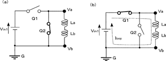
図4は、循環電流が発生する要因について詳細に説明するための図である。同図においては、図1におけるインバータ装置20a,20bのDC/DCコンバータ回路21、インバータ回路22、及びフィルタ回路23が、それぞれ、昇圧チョッパ部、三相フルブリッジインバータ部、及びLCLフィルタ部である場合のインバータ装置a,bの回路図を示している。また、説明を簡略化するため、昇圧チョッパ部の特性は同一とし、インバータ装置aのスイッチング素子Q1〜Q6、及びインバータ装置bのスイッチング素子Q1〜Q6のスイッチングパターンは同一とした上で、スイッチング素子Q1、Q2の状態にのみ着目する。なお、ここでの説明は、循環電流のほんの一例であり、実際には昇圧チョッパ部、及び三相フルブリッジインバータ部のスイッチングパターンの組み合わせにより、多種多様な経路で循環電流が発生する。
FIG. 4 is a diagram for explaining in detail the factors that cause the circulating current. In FIG. 1, the DC /
インバータ装置a、b間において、インバータ装置a、bともにスイッチング素子Q1がオン、Q2がオフの状態を考えると、直流電源側から昇圧チョッパ部を通じてエネルギーがフィルタLCL1に蓄積されるモードとなっている(図4(a)参照)。ここで、直流電源からの入力電力Pin1、Pin2に差が発生している場合、各インバータ装置a、b内のフィルタLCL1に蓄積されるエネルギーに差が発生することになる。 Considering the state where the switching element Q1 is on and the switching element Q2 is off between the inverter devices a and b, the energy is stored in the filter LCL1 from the DC power supply side through the step-up chopper unit. (See FIG. 4 (a)). Here, when a difference is generated between the input powers Pin1 and Pin2 from the DC power source, a difference is generated in the energy accumulated in the filter LCL1 in each of the inverter devices a and b.
次に、スイッチング素子Q1がオフ、Q2がオン状態に切り変わった場合を考える(図4(b)参照)。この場合、同図に示す循環電流経路が形成される(同図に示す太線の経路)。直流電源からの入力電力Pin1、Pin2に電力差がない場合は、各インバータ装置a、b内のフィルタLCL1の両端電圧に蓄積エネルギー差による電位差(=VL1−VL2[V])が発生しない。したがって、循環電流経路が形成されたとしても、循環電流は発生せず、各フィルタLCL1の蓄積エネルギーが全て系統側へ出力される。変換損失を考慮しない場合、出力電力Pout[W]=Pin1+Pin2[W]となる。しかし、直流電源からの入力電力Pin1、Pin2に電力差が発生していると、各インバータ装置a、b内のフィルタLCL1の両端電圧に蓄積エネルギー差による電位差(=VL1−VL2[V])が発生する。この電位差により、図に示す循環電流経路を経由して、インバータ装置a、b間で循環電流が発生してしまう。よって、循環電流分の電力をPloopとすると、Pout[W]=Pin1+Pin2−Ploop[W]となり、循環電流の大きさによっては変換効率を著しく低下させることになる。 Next, consider a case where the switching element Q1 is turned off and Q2 is turned on (see FIG. 4B). In this case, the circulating current path shown in the figure is formed (thick line path shown in the figure). When there is no power difference between the input powers Pin1 and Pin2 from the DC power supply, a potential difference (= V L1 −V L2 [V]) due to the accumulated energy difference does not occur in the voltage across the filter LCL1 in each inverter device a and b. . Therefore, even if a circulating current path is formed, no circulating current is generated, and all the accumulated energy of each filter LCL1 is output to the system side. When conversion loss is not taken into consideration, output power Pout [W] = Pin1 + Pin2 [W]. However, if there is a power difference between the input powers Pin1 and Pin2 from the DC power supply, a potential difference (= V L1 −V L2 [V] due to the accumulated energy difference between the voltages at both ends of the filter LCL1 in each inverter device a and b. ) Occurs. Due to this potential difference, a circulating current is generated between the inverter devices a and b via the circulating current path shown in the figure. Therefore, if the power for the circulating current is Ploop, Pout [W] = Pin1 + Pin2−Ploop [W], and the conversion efficiency is significantly reduced depending on the magnitude of the circulating current.
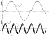
図5は、インバータ装置20aから出力される零相電流Izの波形を説明するための図である。
FIG. 5 is a diagram for explaining the waveform of the zero-phase current Iz output from the
図5の上段に示す正弦波状の波形は、インバータ装置20aのU相の出力ラインから出力されるU相電流Iuの波形の一例を示している。U相電流Iuには循環電流Iが重畳されているので、理想的な正弦波になっていない。V相およびW相の出力ラインから出力されるV相電流およびW相電流の波形も同様の波形となる。一方、図5の下段に示す正弦波状の波形は、循環電流Iが流れているときのインバータ装置20aから出力される零相電流Izの波形の一例を示している。零相電流Izは、U相電流Iu、V相電流Iv、およびW相電流Iwを加算したものであり、直流電源10a,10b、10cとインバータ装置20a,20b、20cの対地間の静電容量等が無視できるレベルであれば、零相電流Izは循環電流Iとみなせる。なお、循環電流Iが流れていないときの零相電流Iz'は、図5の点線で示すようにゼロになる。
The sinusoidal waveform shown in the upper part of FIG. 5 shows an example of the waveform of the U-phase current Iu output from the U-phase output line of the
循環電流として流れる電流には、直流成分、U相電流Iuの3次高調波成分、およびスイッチング周波数(キャリア信号の周波数であり、例えば、4kHz)を有する高周波成分の3種類があるので、零相電流Izはこれらの混合した交流電流となる。したがって、図5に示すように、循環電流Iが流れているときの零相電流Izは、U相電流Iuの3次高調波成分にキャリア信号の周波数を有する高周波成分が重畳した、直流成分Iaveのレベルを中心に振幅が変動する交流信号となる。 There are three types of current flowing as a circulating current: a direct current component, a third harmonic component of the U-phase current Iu, and a high-frequency component having a switching frequency (the frequency of the carrier signal, for example, 4 kHz). The current Iz becomes a mixed alternating current. Therefore, as shown in FIG. 5, the zero-phase current Iz when the circulating current I is flowing is a DC component Iave in which a high-frequency component having the frequency of the carrier signal is superimposed on the third-order harmonic component of the U-phase current Iu. The AC signal varies in amplitude around the level of.
本発明においては、零相電流Izに重畳されているこれらの循環電流を抑制するための構成を、各インバータ装置20a,20b,20cに取り入れている。具体的には、各インバータ装置20a,20b,20cから出力される出力電流の零相電流Izに含まれる上記の3次成分、高周波成分をそれぞれゼロに抑制するフィードバック制御系を各インバータ装置20a,20b,20cの制御回路24にそれぞれ設け、各制御回路24が出力するPWM信号の位相を一致させて直流成分を抑制するようにしている。
In the present invention, a configuration for suppressing these circulating currents superimposed on the zero-phase current Iz is incorporated in each of the
次に、高周波成分を抑制するための構成が取り入れられた制御回路を備えた第3実施形態について説明する。まず、高周波成分の零相電流Izが流れる原因について説明する。 Next, a third embodiment including a control circuit incorporating a configuration for suppressing high frequency components will be described. First, the cause of the flow of the high-frequency component zero-phase current Iz will be described.
図6は、高周波成分の循環電流の循環経路について説明するための図である。同図は、図4に示す回路図に、直流電源10a,10bを追加した回路図である。説明を簡略化するため、直流電源からの入力電圧は同一(Vin1=Vin2)とし、昇圧チョッパ部は停止状態として、インバータ装置a、bのスイッチング素子Q1、Q2の状態にのみ着目する。インバータ装置aのスイッチング素子Q1とインバータ装置bのスイッチング素子Q1とが同じタイミングでオンとオフの切り替えを行っている場合(インバータ装置aのスイッチング素子Q2とインバータ装置bのスイッチング素子Q2とも同じタイミングでオンとオフの切り替えを行っている)、各インバータ装置a,bのVa,Vbのポイントでの電圧(以下、「出力電圧Va,Vb」とする)は、Vin1(=Vin2)又は接地電位に固定されるので、循環電流は発生しない。ここで、各インバータ装置a、bのスイッチング素子Q1、Q2のオンとオフの切り替えタイミングが一致しない場合、すなわち、インバータ装置a、bに入力されるPWM信号に位相差が発生している場合を考える。
FIG. 6 is a diagram for explaining the circulation path of the circulating current of the high-frequency component. This figure is a circuit diagram in which
図7は、インバータ装置a、bに入力されるPWM信号に位相差が発生している場合の、出力電圧Va,Vbの電圧波形を示している。同図に示すように、入力されるPWM信号の位相差により、期間P1および期間P3において出力電圧Va,Vbに電圧差が生じている。 FIG. 7 shows voltage waveforms of the output voltages Va and Vb when a phase difference is generated in the PWM signals input to the inverter devices a and b. As shown in the figure, there is a voltage difference between the output voltages Va and Vb in the period P1 and the period P3 due to the phase difference between the input PWM signals.
ここで、同図に示すP1の期間にのみ着目して説明を行う。Va及びVbがゼロ(すなわちインバータ装置bのスイッチング素子Q1がオフ、スイッチング素子Q2がオンの状態)継続中に、Vaが上昇(すなわちインバータ装置aのスイッチング素子Q1がオン、スイッチング素子Q2がオフ)した状態を、簡略化した等価回路図で説明する。 Here, description will be given focusing on only the period P1 shown in FIG. Va rises (ie, switching element Q1 of inverter device a is on and switching element Q2 is off) while Va and Vb continue to be zero (that is, switching element Q1 of inverter device b is off and switching element Q2 is on). This state will be described with a simplified equivalent circuit diagram.
図8は、図6におけるVbがゼロの状態の簡略化した等価回路図である。同図において、フィルタLCL1については、L成分のみを記載しており、インバータ装置aのフィルタLCL1のインダクタンス値をLa、インバータ装置bのフィルタLCL1のインダクタンス値をLbとしている。 FIG. 8 is a simplified equivalent circuit diagram in a state where Vb in FIG. 6 is zero. In the figure, only the L component is described for the filter LCL1, the inductance value of the filter LCL1 of the inverter device a is La, and the inductance value of the filter LCL1 of the inverter device b is Lb.
同図(a)は、Va、Vbともにゼロの状態を示している。初期条件としてLa、Lbにはエネルギー蓄積はないもの(初期電流はゼロ)とする。この状態からP1の期間に遷移(すなわちQ1がオン、Q2がオフ)した場合、Va、Vb間に直流電源電圧Vin1が印加されることにより、La、Lbを経由して循環電流Iloopが発生する(同図(b)参照)。この時の循環電流Iloopは、インダクタの特性を示す公知の下記(1)式に基づいて、下記(2)式で算出される。 FIG. 5A shows a state where Va and Vb are both zero. As an initial condition, La and Lb are assumed to have no energy accumulation (initial current is zero). When a transition is made from this state to the period P1 (ie, Q1 is on and Q2 is off), a circulating current I loop is generated via La and Lb by applying the DC power supply voltage Vin1 between Va and Vb. (Refer to (b) in the figure). The circulating current I loop at this time is calculated by the following equation (2) based on the well-known equation (1) showing the characteristics of the inductor.

上記(2)式より明らかであるが、tが大きいほど(PWM信号の位相差が大きく、同図(b)の状態が長く続くほど)、高周波の循環電流のピーク値は増大する。 As is apparent from the above equation (2), the peak value of the high-frequency circulating current increases as t increases (the phase difference of the PWM signal increases and the state shown in FIG. 2B continues longer).
よって、期間P1においては、インバータ装置aの出力電圧Vaの方がインバータ装置bの出力電圧Vbより高いので、インバータ装置aからインバータ装置bに循環電流が流れる。一方、これとは逆に、期間P3においては、出力電圧Vbの方が出力電圧Vaより高いので、インバータ装置bからインバータ装置aに循環電流が流れる。なお、期間P2およびP4においては、出力電圧Vaと出力電圧Vbとが同電位となるので、インバータ装置aとインバータ装置bとの間で循環電流は流れない。PWM信号の周波数(スイッチング周波数)が例えば4kHzの場合、期間P1からP4までの時間は(1/4000)秒なので、インバータ装置20aからインバータ装置20bに流れる循環電流は4kHzの高周波電流となる。したがって、PWM信号の位相が一致しない場合には、当該PWM信号の周波数を有する高周波の循環電流が出力電流に重畳される。これにより、零相電流Izは、高周波成分の循環電流が重畳されたものとなる(図5参照)。
Therefore, in the period P1, since the output voltage Va of the inverter device a is higher than the output voltage Vb of the inverter device b, a circulating current flows from the inverter device a to the inverter device b. On the other hand, in the period P3, since the output voltage Vb is higher than the output voltage Va in the period P3, a circulating current flows from the inverter device b to the inverter device a. In the periods P2 and P4, since the output voltage Va and the output voltage Vb are the same potential, no circulating current flows between the inverter device a and the inverter device b. When the frequency (switching frequency) of the PWM signal is 4 kHz, for example, the time from the period P1 to P4 is (1/4000) seconds, so the circulating current flowing from the
第3実施形態では、各インバータ装置20a,20b,20cの制御部24から出力されるPWM信号の位相を一致させることにより、スイッチング周波数の高周波成分の循環電流を抑制する。第3実施形態では、インバータ装置20aがインバータ装置20b,20cを統括的に制御しており、インバータ装置20aが本発明の「マスタインバータ装置」に対応し、インバータ装置20b,20cが本発明の「スレーブインバータ装置」に対応する。
In 3rd Embodiment, the circulating current of the high frequency component of switching frequency is suppressed by making the phase of the PWM signal output from the
図9は、本発明に係る系統連系インバータシステムの第3実施形態を説明するための図である。同図においては、制御回路24の内部構成の一部のみを記載している。なお、制御回路24以外の構成は、図1に示す系統連系インバータシステムAと同様であるので、記載を省略している。また、同図において、インバータ装置20a,20b,20cの制御回路24を、それぞれ制御回路24a,24b,24cとしている。
FIG. 9 is a diagram for explaining a third embodiment of the grid-connected inverter system according to the present invention. In the figure, only a part of the internal configuration of the
制御回路24aは、内部発振部1a、キャリア信号生成部2a、およびPWM信号生成部3a、位相補正部4aを備えている。内部発振部1aは、所定の周波数(例えば4kHz)のクロックパルス信号CLKを生成するものである。内部発振部1aは、生成したクロックパルス信号CLKをキャリア信号生成部2aおよび位相補正部4aに出力する。キャリア信号生成部2aは、内部発振部1aから入力されるクロックパルス信号CLKに基づいて、キャリア信号CRを生成するものである。キャリア信号生成部2aは、生成したキャリア信号CRをPWM信号生成部3aに出力する。
The
PWM信号生成部3aは、キャリア信号生成部2aから入力されるキャリア信号CRと、図示しない指令値信号生成部から入力される指令値信号とから、三角波比較法によりPWM信号PWM1を生成するものである。PWM信号生成部3aは、生成したPWM信号PWM1をインバータ回路22に出力する。なお、指令値信号生成部は、指令値信号を各相(U相,V相,W相)ごとに生成して、PWM信号生成部3aに出力する。PWM信号生成部3aは、各相に対する指令値信号とキャリア信号CRとの比較により、各相に対する3つのPWM信号を生成する。また、PWM信号生成部3aは、生成された3つのPWM信号をそれぞれ反転させたPWM信号も生成する。PWM信号PWM1は、これらの6つのPWM信号を含む信号として表している。
The PWM
位相補正部4aは、内部発振部1aから入力されるクロックパルス信号CLKの位相を進めたクロックパルス信号CLK’を生成するものである。位相補正部4aは、クロックパルス信号CLK’を、制御回路24b,24cに出力する。第3実施形態においては、各制御回路24a,24b,24c間の信号の入出力を、I/Oポートを介して行っている。この場合、フォトカプラ等の素子によって信号の位相が遅延する。位相補正部4aは、この位相の遅延分を補正するために、クロックパルス信号CLKから位相を進めたクロックパルス信号CLK’を生成している。
The
図10は、クロックパルス信号CLKの位相補正を説明するための図である。同図(a)は、内部発振部1aから出力されるクロックパルス信号CLKを示している。同図(b)は、位相補正部4aから出力されるクロックパルス信号CLK’を示している。クロックパルス信号CLK’は、クロックパルス信号CLKより所定値θだけ位相が進められている。所定値θは、I/Oポートを介する信号の位相の遅延に応じて、あらかじめ実験により適切な値に設定される。同図(c)は、制御回路24b,24cのキャリア信号生成部2b,2c(後述)にそれぞれ入力されるクロックパルス信号CLK”を示している。制御回路24aから出力される信号は制御回路24b,24cに入力されるまでに位相がθだけ遅延するので、クロックパルス信号CLK”は、クロックパルス信号CLK’より所定値θだけ位相が遅れている。これにより、キャリア信号生成部2aに入力されるクロックパルス信号CLKと位相が一致するクロックパルス信号CLK”が、キャリア信号生成部2b,2cに入力される。
FIG. 10 is a diagram for explaining the phase correction of the clock pulse signal CLK. FIG. 5A shows the clock pulse signal CLK output from the
図9に戻って、制御回路24bは、キャリア信号生成部2bおよびPWM信号生成部3bを備えている。キャリア信号生成部2bおよびPWM信号生成部3bは、制御回路24aのキャリア信号生成部2aおよびPWM信号生成部3aと同様の機能を果たす。キャリア信号生成部2bには、位相補正部4aより出力されるクロックパルス信号CLK’から位相が遅延したクロックパルス信号CLK”が入力される。上述したように、クロックパルス信号CLK’は、内部発振部1aから出力されるクロックパルス信号CLKを、各制御回路24a,24b,24c間での入出力時に遅延する位相θだけ予め進めた信号である。したがって、クロックパルス信号CLK”は、クロックパルス信号CLKと位相が一致した信号となる。これにより、PWM信号生成部3bで生成されるPWM信号PWM2の位相は、PWM信号生成部3aで生成されるPWM信号PWM1の位相と一致する。
Returning to FIG. 9, the
制御回路24cは、キャリア信号生成部2cおよびPWM信号生成部3cを備えている。キャリア信号生成部2cおよびPWM信号生成部3cは、制御回路24aのキャリア信号生成部2aおよびPWM信号生成部3aと同様の機能を果たす。キャリア信号生成部2cに入力されるクロックパルス信号CLK”もクロックパルス信号CLKと位相が一致した信号となっているので、PWM信号生成部3cで生成されるPWM信号PWM3の位相は、PWM信号生成部3aで生成されるPWM信号PWM1の位相と一致する。
The
第3実施形態においても、システムに用いる変圧器の数を抑制することができるので、上記第1および第2実施形態と同様の作用効果を奏することができる。さらに、第3実施形態においては、制御回路24a,24b,24cからそれぞれ出力されるPWM信号PWM1,PWM2,PWM3の位相が一致している。したがって、各インバータ装置20a,20b,20cの間で循環電流の電流経路が形成されても、スイッチング周波数の高周波成分の循環電流を抑制することができる。その結果、零相電流Izに重畳される高周波成分の循環電流が抑制される。
Also in 3rd Embodiment, since the number of the transformers used for a system can be suppressed, there can exist an effect similar to the said 1st and 2nd embodiment. Furthermore, in the third embodiment, the phases of the PWM signals PWM1, PWM2, and PWM3 output from the
なお、第3実施形態では、制御回路24aから制御回路24bに出力される信号の位相の遅延と、制御回路24aから制御回路24cに出力される信号の位相の遅延とが同じ場合について説明しているが、両者の遅延位相が異なる場合は、それぞれの遅延位相に応じて位相を補正するようにすればよい。すなわち、制御回路24aから制御回路24bに出力される信号の位相の遅延を補正する位相補正部と、制御回路24aから制御回路24cに出力される信号の位相の遅延を補正する位相補正部とを設ければよい。
In the third embodiment, the case where the phase delay of the signal output from the
図11は、第3実施形態における別の実施例(以下では、上記に説明した図9に示す実施例を第1実施例とし、本実施例を第2実施例とする。)を説明するための図である。なお、同図において、図9に示す第1実施例と同一または類似の要素には、同一の符号を付している。 FIG. 11 illustrates another example of the third embodiment (hereinafter, the example illustrated in FIG. 9 described above is referred to as a first example, and this example is referred to as a second example). FIG. In the figure, the same or similar elements as those in the first embodiment shown in FIG.
図11に示す第2実施例では、位相補正部が2個設けられている点で、第1実施例と異なる。位相補正部41aは、内部発振部1aから入力されるクロックパルス信号CLKの位相を、制御回路24aから制御回路24bに出力される信号の遅延位相θ’だけ進めたクロックパルス信号CLK1’を生成して出力するものである。位相補正部41aから出力されたクロックパルス信号CLK1’は、位相θ’だけ遅れたクロックパルス信号CLK1”として、キャリア信号生成部2bに入力される。クロックパルス信号CLK1”は、クロックパルス信号CLKと位相が一致した信号となるので、PWM信号生成部3bで生成されるPWM信号PWM2の位相は、PWM信号生成部3aで生成されるPWM信号PWM1の位相と一致する。
The second embodiment shown in FIG. 11 differs from the first embodiment in that two phase correction units are provided. The
位相補正部42aは、内部発振部1aから入力されるクロックパルス信号CLKの位相を、制御回路24aから制御回路24cに出力される信号の遅延位相θ”だけ進めたクロックパルス信号CLK2’を生成して出力するものである。位相補正部42aから出力されたクロックパルス信号CLK2’は、位相θ”だけ遅れたクロックパルス信号CLK2”として、キャリア信号生成部2cに入力される。クロックパルス信号CLK2”は、クロックパルス信号CLKと位相が一致した信号となるので、PWM信号生成部3cで生成されるPWM信号PWM3の位相は、PWM信号生成部3aで生成されるPWM信号PWM1の位相と一致する。
The
第2実施例においては、制御回路24aから制御回路24bに出力される信号の遅延位相θ’と、制御回路24aから制御回路24cに出力される信号の遅延位相θ”とが異なる場合でも、制御回路24a,24b,24cからそれぞれ出力されるPWM信号PWM1,PWM2,PWM3の位相を一致させることができ、スイッチング周波数の高周波成分の循環電流を抑制することができる。その結果、零相電流Izに重畳される高周波成分の循環電流が抑制される。
In the second embodiment, control is performed even when the delay phase θ ′ of the signal output from the
なお、上記第1および第2実施例では、クロックパルス信号を出力する側の制御回路24aに位相補正部を設けた場合について説明しているが、クロックパルス信号を入力される側の制御回路24b,24cに位相補正部を設けるようにしてもよい。
In the first and second embodiments, the case where the phase correction unit is provided in the
図12は、第3実施形態における第3実施例を説明するための図である。なお、同図において、図11に示す第2実施例と同一または類似の要素には、同一の符号を付している。 FIG. 12 is a diagram for explaining a third example of the third embodiment. In the figure, the same or similar elements as those in the second embodiment shown in FIG.
図12に示す第3実施例では、制御回路24aに位相補正部41a,42aが設けられる代わりに、制御回路24b,24cにそれぞれ位相補正部4b,4cが設けられている点で、第2実施例と異なる。
In the third embodiment shown in FIG. 12, in place of the
第3実施例においても、制御回路24aから制御回路24bに出力される信号の遅延位相θ’と、制御回路24aから制御回路24cに出力される信号の遅延位相θ”とが異なる場合でも、制御回路24a,24b,24cからそれぞれ出力されるPWM信号PWM1,PWM2,PWM3の位相を一致させることができ、スイッチング周波数の高周波成分の循環電流を抑制することができる。その結果、零相電流Izに重畳される高周波成分の循環電流が抑制される。
Even in the third embodiment, even when the delay phase θ ′ of the signal output from the
なお、上記第1ないし第3実施例では、制御回路24aから制御回路24b,24cにクロックパルス信号を出力する場合について説明しているが、キャリア信号を出力するようにしてもよい。
In the first to third embodiments, the case where the clock pulse signal is output from the
図13は、第3実施形態における第4実施例を説明するための図である。なお、同図において、図9に示す第1実施例と同一または類似の要素には、同一の符号を付している。 FIG. 13 is a diagram for explaining a fourth example of the third embodiment. In the figure, the same or similar elements as those in the first embodiment shown in FIG.
図13に示す第4実施例では、位相補正部4aがクロックパルス信号CLKの位相を進めて出力する代わりに、キャリア位相補正部4a’がキャリア信号CRの位相を進めて出力する点と、制御回路24b,24cにキャリア信号生成部2b,2cを設けていない点で、第1実施例と異なる。
In the fourth embodiment shown in FIG. 13, instead of the
キャリア位相補正部4a’は、キャリア信号生成部2aから入力されるキャリア信号CRの位相を所定値θだけ進めたキャリア信号CR’を生成するものである。キャリア位相補正部4a’は、キャリア信号CR’を、制御回路24b,24cに出力する。PWM信号生成部3b,3cには、キャリア位相補正部4a’より出力されるキャリア信号CR’から位相θだけ遅延したキャリア信号CR”が入力される。キャリア信号CR”は、キャリア信号CRと位相が一致した信号となる。これにより、PWM信号生成部3b,3cで生成されるPWM信号PWM2,PWM3の位相は、PWM信号生成部3aで生成されるPWM信号PWM1の位相と一致する。
The carrier
第4実施例においても、制御回路24a,24b,24cからそれぞれ出力されるPWM信号PWM1,PWM2,PWM3の位相を一致させることができ、スイッチング周波数の高周波成分の循環電流を抑制することができる。その結果、零相電流Izに重畳される高周波成分の循環電流が抑制される。なお、第4実施例においても、図11と同様に、制御回路24a内にキャリア位相補正部を2個設けて、キャリア信号CRをそれぞれ対応する位相θ’,θ”だけ進めて制御回路24b,24cに出力するようにしてもよい。また、キャリア位相補正部を制御回路24aに設ける代わりに、図12と同様に、制御回路24b,24cにそれぞれ設けるようにしてもよい。
Also in the fourth embodiment, the phases of the PWM signals PWM1, PWM2, and PWM3 output from the
なお、制御回路24aの内部発振部1aからキャリア信号生成部2aに入力されるクロックパルス信号CLKと、制御回路24b,24c内のキャリア信号生成部2b,2cにそれぞれ入力されるクロックパルス信号との位相のずれが小さく、それに起因する、PWM信号生成部3a,3b,3cでそれぞれ生成されるPWM信号相互の位相差が特に問題とならない場合は、位相補正部を省略することができる。キャリア信号の位相のずれに起因する場合も同様に、PWM信号生成部3a,3b,3cでそれぞれ生成されるPWM信号相互の位相差が特に問題とならない場合は、キャリア位相補正部を省略することができる。
The clock pulse signal CLK input from the
なお、第3実施形態では、インバータ装置が3台並列接続されている場合について説明しているが、接続されるインバータ装置が2台の場合や4台以上の場合でも、本発明を適用することができる。また、各インバータ装置にそれぞれ別の直流電源が接続されている場合(図1参照)でも、1つの直流電源の出力を分配して各インバータ装置に入力する場合(図2参照)でも、本発明を適用することができる。 In the third embodiment, the case where three inverter devices are connected in parallel is described. However, the present invention is applied even when there are two inverter devices or four or more inverter devices connected. Can do. Even when separate DC power supplies are connected to the respective inverter devices (see FIG. 1), the present invention can be applied to the case where the output of one DC power supply is distributed and input to each inverter device (see FIG. 2). Can be applied.
次に、本発明に係る系統連系インバータシステムの第4実施形態について説明する。 Next, a fourth embodiment of the grid-connected inverter system according to the present invention will be described.
図14は、直流成分の循環電流の循環経路について説明するための図である。同図は、太線で示す循環電流の循環経路のみが、図6に示す回路図と異なる。説明の簡略化のため、直流電源側の特性は同一とし(出力電力が同じ)、インバータ装置a、bの三相フルブリッジインバータ部のスイッチングパターンも同一として考える。インバータ装置a、b間の違いはバス電圧差のみとする。バス電圧は、図14に示すインバータ装置a、b内のコンデンサC1の両端電圧Vbus1、Vbus2となる。このバス電圧を一定にするため、昇圧チョッパ部、及び三相フルブリッジインバータ部のスイッチングが制御されている。 FIG. 14 is a diagram for explaining the circulation path of the circulation current of the DC component. This figure is different from the circuit diagram shown in FIG. 6 only in the circulation path of the circulating current indicated by a bold line. For simplification of explanation, the characteristics on the DC power supply side are assumed to be the same (the output power is the same), and the switching patterns of the three-phase full-bridge inverter portions of the inverter devices a and b are also assumed to be the same. The difference between the inverter devices a and b is only the bus voltage difference. The bus voltages are the voltages Vbus1 and Vbus2 across the capacitor C1 in the inverter devices a and b shown in FIG. In order to make this bus voltage constant, switching of the step-up chopper section and the three-phase full-bridge inverter section is controlled.
この時、バス電圧検出回路のバラツキによる制御誤差等により、インバータ装置a、bのバス電圧に差が発生すると、例えばインバータ装置aのバス電圧Vbus1がインバータ装置bのバス電圧Vbus2よりも高い場合(Vbus1>Vbus2)、同図に示す太線の循環経路を流れる循環電流Iloopが発生する。なお、図14に示す循環経路は、スイッチング素子Q1、Q2の状態のみに着目した場合のものである。このように、スイッチング素子の状態を限定すると、図14に示す回路図は図15に示す等価回路図に変換して考えることができる。同図においては、インバータ装置a、bのコンデンサC1を含めた昇圧チョッパ部を理想的な直流電源と内部抵抗で置き換え、フィルタLCL1についてはL成分のみで置換し、インバータ装置aのフィルタLCL1のインダクタンス値をLa、インバータ装置bのフィルタLCL1のインダクタンス値をLbとしている。 At this time, if a difference occurs in the bus voltage of the inverter devices a and b due to a control error due to variations in the bus voltage detection circuit, for example, the bus voltage Vbus1 of the inverter device a is higher than the bus voltage Vbus2 of the inverter device b ( Vbus1> Vbus2), a circulating current I loop flowing through the thick circulation path shown in FIG. In addition, the circulation path shown in FIG. 14 is a thing at the time of paying attention only to the state of switching element Q1, Q2. As described above, when the states of the switching elements are limited, the circuit diagram shown in FIG. 14 can be converted into the equivalent circuit diagram shown in FIG. In the figure, the step-up chopper part including the capacitor C1 of the inverter devices a and b is replaced with an ideal DC power supply and an internal resistance, the filter LCL1 is replaced only with the L component, and the inductance of the filter LCL1 of the inverter device a The value is La, and the inductance value of the filter LCL1 of the inverter device b is Lb.
Vbus1=Vbus2の場合を考えると、インバータ装置a、bのスイッチング素子Q1、Q2のスイッチングパターンが同一であるので、インバータ装置a、b間に循環電流は発生しない。しかし、Vbus1>Vbus2の場合、同図(a)に示すように、スイッチング素子のQ1がオン、Q2がオフの状態でインバータ装置aからbへの循環電流が発生する。このとき、インバータ装置a、bのスイッチング素子のQ1がオフに、Q2がオンに同時に切り替わると、同図(b)に示すように、La、Lbのインダクタンス作用により、インバータ装置aからbに継続して循環電流が同方向に流れる。すなわち、同図(a)と同図(b)の状態が交互に切り替わることで、同方向に流れる直流成分の循環電流が継続して発生する。 Considering the case of Vbus1 = Vbus2, since the switching patterns of the switching elements Q1 and Q2 of the inverter devices a and b are the same, no circulating current is generated between the inverter devices a and b. However, when Vbus1> Vbus2, a circulating current is generated from the inverter devices a to b with the switching element Q1 on and Q2 off as shown in FIG. At this time, when Q1 of the switching elements of the inverter devices a and b are simultaneously switched off and Q2 is switched on, the inverter devices a to b are continued by the inductance action of La and Lb as shown in FIG. Circulating current flows in the same direction. In other words, by alternately switching the states of FIG. 5A and FIG. 5B, a DC component circulating current flowing in the same direction is continuously generated.
よって、零相電流Iz(図5参照)に重畳される直流成分の循環電流は、各インバータ装置20a,20b,20cのバス電圧の間に差が生じた場合に発生する。第4実施形態では、各インバータ装置20a,20b,20cにおいて、出力電流の零相電流Izから直流成分を抽出して、これをゼロにフィードバック制御するための補正値をバス電圧の目標値に加算することで、直流成分の循環電流を抑制する。
Therefore, the DC component circulating current superimposed on the zero-phase current Iz (see FIG. 5) is generated when a difference occurs between the bus voltages of the
図16は、本発明に係る系統連系インバータシステムの第4実施形態を説明するための図である。同図においては、インバータ装置20aの内部構成のみを記載している。なお、インバータ装置20b、20cの内部構成はインバータ装置20aと同様であり、その他の構成は図1に示す系統連系インバータシステムAと同様であるので、記載を省略している。また、制御回路24の内部構成のうち第4実施形態の上記の要点に特に関係しない構成(内部発振部1a,キャリア信号生成部2aなど)についても、記載を省略している。
FIG. 16 is a diagram for explaining a fourth embodiment of the grid-connected inverter system according to the present invention. Only the internal configuration of the
同図に示すインバータ装置20aには、フィルタ回路23の出力側に零相電流検出回路26が設けられている。零相電流検出回路26は、フィルタ回路23から出力される各相(U相,V相,W相)の交流電流を検出し、検出された各相の交流電流信号を加算することで零相電流信号を生成して制御回路24に出力する。バス電圧検出回路25は、DC/DCコンバータ回路21から出力されるバス電圧を検出し、検出されたバス電圧信号を制御回路24に出力するものであり、図1において記載を省略していた検出回路である。
In the
制御回路24は、直流成分抽出部5、指令値信号生成部6、およびPWM信号生成部3を備えている。直流成分抽出部5は、零相電流検出回路26より入力される零相電流信号から交流成分を除去して直流成分を抽出するものであり、ローパスフィルタを備えている。直流成分抽出部5は、抽出された零相電流信号の直流成分を指令値信号生成部6に出力する。
The
指令値信号生成部6は、バス電圧検出回路25から入力されるバス電圧信号と、その目標値であるバス電圧目標値と、直流成分抽出部5から入力される零相電流信号の直流成分とから、指令値信号を生成して、PWM信号生成部3に出力するものである。
The command value
指令値信号生成部6は、PI制御部61,62、および電流制御部63を備えている。PI制御部61は、零相電流信号の直流成分をゼロにフィードバック制御するためのものである。PI制御部61は、直流成分抽出部5から零相電流信号の直流成分を入力され、PI制御を行って、補正値を出力する。当該補正値は、バス電圧目標値に加算される(以下では、当該補正値が加算されたバス電圧目標値を、「補正目標値」とする。)。PI制御部62は、インバータ装置20aのバス電圧を補正目標値にフィードバック制御するためのものである。PI制御部62は、バス電圧検出回路25より入力されるバス電圧信号と補正目標値との偏差を入力され、PI制御を行って、補正値を電流制御部63に出力する。電流制御部63は、フィルタ回路23から出力される各相の交流電流を目標電流にフィードバック制御するためのものである。電流制御部63は、PI制御部62から入力される補正値に基づいて各相の指令値信号を生成して、PWM信号生成部3に出力する。具体的には、フィルタ回路23から出力される各相の交流電流を検出した各交流電流信号と、PI制御部62から入力される補正値を加算された目標電流値との偏差をゼロにするための補正値を指令値信号として出力する。
The command value
PWM信号生成部3は、先述したように、図示しないキャリア信号生成部から入力されるキャリア信号CRと、指令値信号生成部6から入力される指令値信号とから、PWM信号PWM1を生成するものである。PWM信号生成部3は、生成したPWM信号PWM1をインバータ回路22に出力する。
As described above, the PWM
第4実施形態においても、用いる変圧器の数を抑制することができるので、上記第1および第2実施形態と同様の作用効果を奏することができる。さらに、第4実施形態においては、零相電流信号の直流成分がゼロにフィードバック制御されるので、各インバータ装置20a,20b,20cの間で電流経路が形成されても、直流成分の循環電流を抑制することができる。
Also in the fourth embodiment, since the number of transformers to be used can be suppressed, the same operational effects as those in the first and second embodiments can be obtained. Furthermore, in the fourth embodiment, since the DC component of the zero-phase current signal is feedback-controlled to zero, even if a current path is formed between the
なお、第4実施形態では、零相電流検出回路26を、フィルタ回路23から出力される各相の交流電流を検出し、検出された各相の交流電流信号を加算することで零相電流信号を生成する構成としているが、これに限られない。例えば、零相電流検出回路26を、零相変流器としてもよい。また、図17に示すように、直流電源側の接地ライン上を流れる電流を検出する循環電流検出回路を設け、直流成分抽出部5へ入力することにより、同様の効果を得ることができる。また、指令値信号生成部6の内部構成は上記に限定されず、直流成分抽出部5から入力される零相電流信号の直流成分をゼロにフィードバック制御するための指令値信号を生成する構成であればよい。
In the fourth embodiment, the zero-phase
なお、第4実施形態では、直流成分の循環電流の抑制制御を、すべてのインバータ装置20a,20b,20cで行っているが、これに限られない。インバータ装置20a,20b,20cのうちのいずれか1つ(例えば、インバータ装置20a)のみで抑制制御を行うようにしてもよい。この場合でも、1つのインバータ装置の零相電流信号の直流成分が抑制されるので、各インバータ装置20a,20b,20cの間で電流経路が形成されても、直流成分の循環電流を抑制することができる。
In addition, in 4th Embodiment, although suppression control of the circulating current of a DC component is performed by all the
また、インバータ装置20a,20b,20cのうちのいずれか1つ(例えば、インバータ装置20a)のみで抑制制御を行わないようにしても構わない。この場合でも、残り2つのインバータ装置の零相電流信号の直流成分が抑制されるので、各インバータ装置20a,20b,20cの間で電流経路が形成されても、直流成分の循環電流を抑制することができる。また、全てのインバータ装置20a,20b,20cが同時に循環電流抑制を行うことにより制御が安定しなくなる(制御が干渉しあって制御の収束ポイントが定まらない)という不都合を回避することができる。
In addition, the suppression control may not be performed by only one of the
次に、本発明に係る系統連系インバータシステムの第5実施形態について説明する。 Next, a fifth embodiment of the grid-connected inverter system according to the present invention will be described.
一般的に、太陽光発電用の系統連系インバータシステムにおいては、太陽電池の出力電力を有効に取り出すために最大電力点追従制御(以下、「Pmax制御」とする。)が標準装備されることが多い。Pmax制御は太陽電池アレイ毎に行えば高効率化が実現できるため、本発明のシステムを太陽電池に適用した場合、図1の構成により各インバータ装置20a,20b,20cがそれぞれ独立してPmax制御を行った方がよい。よって、このような場合においては、各インバータ装置20a,20b,20cの制御回路24が出力するPWM信号のパターンが異なることになる。
Generally, in a grid-connected inverter system for photovoltaic power generation, maximum power point tracking control (hereinafter referred to as “Pmax control”) is provided as a standard in order to effectively extract the output power of the solar cell. There are many. If the Pmax control is performed for each solar cell array, high efficiency can be realized. Therefore, when the system of the present invention is applied to a solar cell, each
例えば、インバータ装置20aに接続された太陽電池アレイ(図1において、直流電源10aに対応する)の出力電力に対して、インバータ装置20bに接続された太陽電池アレイ(図1において、直流電源10bに対応する)の出力電力の方が大きい場合、インバータ装置20aと比較してインバータ装置20bのPWM信号のデューティ幅(パルスのオン状態の時間の長さ)が大きくなるよう制御される。すなわち、各インバータ装置20a,20b,20c間でPWM信号のオンとオフの切替タイミングのずれが発生し、結果、循環電流が発生することになる。この点においては、第3実施形態で説明した高周波成分の循環電流の発生要因と同じである(図6〜8参照)。但し、このデューティ幅の差に起因する循環電流は、図7に示すPWM信号の位相差による場合と違って、インバータ出力電流の瞬時値の大小に連動して変化する。その結果、インバータ回路22(図1参照)が三相フルブリッジインバータの場合においては、フィルタ回路23等のインピーダンス成分により高周波成分が3次成分に変換されて発生する。
For example, with respect to the output power of the solar cell array connected to the
よって、零相電流Iz(図5参照)に重畳される3次成分の循環電流は、各インバータ装置20a,20b,20cの出力電力に差が生じてPWM信号のデューティ幅が異なってしまうために発生する。第5実施形態では、各インバータ装置20a,20b,20cにおいて、出力電流の零相電流Izから3次成分を抽出して、これをゼロにフィードバック制御するための補正値を指令値信号に加算することにより、3次成分の循環電流を抑制する。
Therefore, the circulating current of the third-order component superimposed on the zero-phase current Iz (see FIG. 5) causes a difference in the output power of each
出力電流の零相電流Izから3次成分を抽出する方法について以下に示す。 A method for extracting the third-order component from the zero-phase current Iz of the output current will be described below.
零相電流検出回路26から入力される零相電流信号を回転角3ωt(なお、ωは、系統電圧の周波数fの角周波数(ω=2πf)である。)で回転する回転座標系に変換すると、同じ回転角3ωtの成分である3次成分が直流成分(以下では、回転座標変換後の直流成分を「直流量」とする。)に変換される。3次成分以外の成分は交流成分(以下では、回転座標変換後の交流成分を「交流量」とする。)に変換されているので、交流量を除去して直流量を抽出することで、3次成分のみを抽出することができる。
When the zero-phase current signal input from the zero-phase
零相電流信号をIz(t)=Asin(3ωt+θ)とし、回転行列[sin3ωt cos3ωt]Tを左側から乗じる。そうすると、下記(3)式により、回転変換後のsin成分αとcos成分βとが算出される。なお、零相電流信号には、高周波成分および直流成分も含まれるが、sin成分αとcos成分βから直流量を抽出したときに除去されるので、説明の簡略化のために省略している。 The zero-phase current signal is set to Iz (t) = Asin (3ωt + θ), and the rotation matrix [sin3ωt cos3ωt] T is multiplied from the left side. Then, the sin component α and the cos component β after rotation conversion are calculated by the following equation ( 3 ). Note that the zero-phase current signal includes a high-frequency component and a direct-current component, but is removed when the direct-current amount is extracted from the sin component α and the cos component β. .
ここで、[α β]Tに対して、直流量を抽出すると、下記(4)式が算出される。[α β]Tはそれぞれ定数値となり、零相電流信号Iz(t)=Asin(3ωt+θ)の振幅A、位相差θを算出することが可能となる。 Here, when the DC amount is extracted with respect to [α β] T , the following equation (4) is calculated. [α β] T is a constant value, and the amplitude A and the phase difference θ of the zero-phase current signal Iz (t) = Asin (3ωt + θ) can be calculated.
また、[α β]Tから零相電流信号Iz(t)を復元する場合は、逆変換行列(2・[sin3ωt cos3ωt])を左側から乗ずることにより、下記(5)式で算出することができる。 When the zero-phase current signal Iz (t) is restored from [α β] T , it can be calculated by the following equation (5) by multiplying the inverse transformation matrix (2 · [sin3ωt cos3ωt]) from the left side. it can.
図18は、本発明に係る系統連系インバータシステムの第5実施形態を説明するための図である。同図においては、制御回路24の内部構成の一部と零相電流検出回路26を記載している。なお、制御回路24および零相電流検出回路26以外の構成は、図1に示す系統連系インバータシステムAと同様であるので、記載を省略している。また、制御回路24の内部構成のうち第5実施形態の説明において必要ない構成(内部発振部1a,キャリア信号生成部2aなど)についても、記載を省略している。
FIG. 18 is a diagram for explaining a fifth embodiment of the grid interconnection inverter system according to the present invention. In the figure, a part of the internal configuration of the
制御回路24は、PWM信号生成部3および指令値信号生成部6を備えている。PWM信号生成部3は、先述したように、図示しないキャリア信号生成部から入力されるキャリア信号CRと、指令値信号生成部6から入力される指令値信号とから、PWM信号PWM1を生成するものであり、生成したPWM信号PWM1をインバータ回路22(図1参照)に出力する。
The
指令値信号生成部6は、零相電流検出回路26から入力される零相電流信号に基づいて指令値信号を生成して、PWM信号生成部3に出力する。指令値信号生成部6は、電流制御部63および零相3次成分制御部64を備えている。電流制御部63は、先述したように、フィルタ回路23(図1参照)から出力される各相の交流電流を目標電流にフィードバック制御するための指令値信号を生成して、PWM信号生成部3に出力する。
The command value
零相3次成分制御部64は、零相電流検出回路26より入力される零相電流信号から3次成分を抽出して、これをゼロにフィードバック制御するための補正値を出力するものである。電流制御部63が出力する指令値信号は、零相3次成分制御部64が出力する補正値を加算されて、PWM信号生成部3に入力される。
The zero-phase third-order
零相3次成分制御部64は、回転変換部641、フィルタ部642,643、PI制御部644,645、補正値生成部646を備えている。
The zero-phase third-order
回転変換部641は、零相電流検出回路26より入力される零相電流信号Iz(t)を、下記(6)式および(7)式に基づいて、sin成分Izs(t)とcos成分Izc(t)に変換するものであり、前述の(3)式に対応する。sin成分Izs(t)はフィルタ部642に出力され、cos成分Izc(t)はフィルタ部642に出力される。
The
Izs(t)=Iz(t)・sin 3ωt ・・・(6)
Izc(t)=Iz(t)・cos 3ωt ・・・(7)
ここで、ω=2πf[rad/s]であり、周波数f[Hz]の値は、PLL等によって、系統電圧の周波数に一致しているものとする。
Izs (t) = Iz (t) · sin 3ωt (6)
Izc (t) = Iz (t) · cos 3ωt (7)
Here, it is assumed that ω = 2πf [rad / s] and the value of the frequency f [Hz] matches the frequency of the system voltage by a PLL or the like.
フィルタ部642は、回転変換部641より入力されるsin成分Izs(t)から交流量を除去して直流量Ysを抽出して出力するものである。フィルタ部643は、回転変換部641より入力されるcos成分Izc(t)から交流量を除去して直流量Xcを抽出して出力するものであり、前述の(4)式に対応する。回転変換部641およびフィルタ部642,643により、零相電流信号の3次成分が直流量に変換されて抽出される。
The
PI制御部644,645は、零相電流信号の3次成分をゼロにフィードバック制御するためのものである。PI制御部644は、フィルタ部642から出力される直流量Ysとその目標値である「0」との偏差を入力され、PI制御を行って、直流量補正値Yspiを出力する。PI制御部645は、フィルタ部643から出力される直流量Xcとその目標値である「0」との偏差を入力され、PI制御を行って、直流量補正値Xcpiを出力する。
The
補正値生成部646は、PI制御部644,645よりそれぞれ入力される直流量補正値Yspiおよび直流量補正値Xcpiを、下記(8)式および(9)式に基づいて、それぞれsin成分補正値Izsr(t)とcos成分補正値Izcr(t)に変換し、これらを加算した補正値Izr(t)を出力するものであり、前述の(5)式に対応する。
The correction
Izsr(t)=2・Yspi・sin(3ωt+φ) ・・・(8)
Izcr(t)=2・Xcpi・cos(3ωt+φ) ・・・(9)
ここで、φは、零相電流検出回路26の遅れ要素や、インバータ回路22の循環電流経路上の遅れ要素(インダクタンス成分)を補償するための値であり、各種インバータ装置に応じて適切な値に設定される。
Izsr (t) = 2 ・ Yspi ・ sin (3ωt + φ) (8)
Izcr (t) = 2 ・ Xcpi ・ cos (3ωt + φ) (9)
Here, φ is a value for compensating for a delay element of the zero-phase
第5実施形態では、3次成分の抑制制御を容易化するため、零相電流信号Iz(t)に回転行列を乗じてから直流量を抽出することで、零相電流信号の3次成分をsin成分とcos成分とに分けて抽出しているが、これに限られない。零相電流信号Iz(t)から直接3次成分を抽出するようにしてもよいし、直流量を抽出せずにそのまま制御するようにしてもよい。 In the fifth embodiment, in order to facilitate the suppression control of the third-order component, the third-order component of the zero-phase current signal is extracted by multiplying the zero-phase current signal Iz (t) by the rotation matrix and then extracting the DC amount. Although it is extracted separately for the sin component and the cos component, it is not limited to this. The tertiary component may be directly extracted from the zero-phase current signal Iz (t), or may be controlled as it is without extracting the DC amount.
第5実施形態においても、用いる変圧器の数を抑制することができるので、上記第1および第2実施形態と同様の作用効果を奏することができる。さらに、第5実施形態においては、零相電流信号の3次成分がゼロにフィードバック制御されるので、各インバータ装置20a,20b,20cの間で電流経路が形成されても、3次成分の循環電流を抑制することができる。
Also in the fifth embodiment, since the number of transformers to be used can be suppressed, the same effects as those in the first and second embodiments can be achieved. Furthermore, in the fifth embodiment, since the tertiary component of the zero-phase current signal is feedback-controlled to zero, even if a current path is formed between the
なお、指令値信号生成部6の内部構成は上記に限定されず、零相電流検出回路26より入力される零相電流信号の3次成分をゼロにフィードバック制御するための指令値信号を生成する構成であればよい。
Note that the internal configuration of the command value
なお、第5実施形態では、3次成分の循環電流の抑制制御を、すべてのインバータ装置20a,20b,20cで行っているが、これに限られない。インバータ装置20a,20b,20cのうちのいずれか1つ(例えば、インバータ装置20a)のみで抑制制御を行うようにしてもよい。この場合でも、1つのインバータ装置の零相電流信号の3次成分が抑制されるので、各インバータ装置20a,20b,20cの間で電流経路が形成されても、3次成分の循環電流を抑制することができる。
In addition, in 5th Embodiment, although suppression control of the circulating current of a tertiary component is performed by all the
また、インバータ装置20a,20b,20cのうちのいずれか1つ(例えば、インバータ装置20a)のみで抑制制御を行わないようにしても構わない。この場合でも、残り2つのインバータ装置の零相電流信号の3次成分が抑制されるので、各インバータ装置20a,20b,20cの間で電流経路が形成されても、3次成分の循環電流を抑制することができる。また、全てのインバータ装置20a,20b,20cが同時に循環電流抑制を行うことにより制御が安定しなくなる(制御が干渉しあって制御の収束ポイントが定まらない)という不都合を回避することができる。
In addition, the suppression control may not be performed by only one of the
なお、上述した第3ないし第5実施形態の3種類の循環電流抑制対策用の回路は、それぞれ抑制対象の循環電流の種類が異なるので、いずれか1つを設ければ、零相電流Izを抑制する効果があるが、いずれか2つを組み合わせた構成もしくは全てを組み合わせた構成にすれば、零相電流Izを可及的にゼロに抑制することができる効果を奏する。 Since the three types of circulating current suppression countermeasure circuits of the third to fifth embodiments described above have different types of circulating currents to be suppressed, if any one is provided, the zero-phase current Iz is reduced. Although there is an effect of suppressing, if a configuration in which any two are combined or a configuration in which all are combined, the zero phase current Iz can be suppressed to zero as much as possible.
図19は、インバータ装置20aの制御回路24aに高周波成分、直流成分及び3次成分をそれぞれ抑制する回路を追加したブロック構成図である。なお、インバータ装置20bの制御回路24bおよびインバータ装置20cの制御回路24cにおけるブロックAの構成は、図19とは異なり、キャリア信号生成部2b、2cのみとなる。
FIG. 19 is a block configuration diagram in which a circuit for suppressing high-frequency components, DC components, and tertiary components is added to the
同図の一点差線で囲むブロックAが高周波成分を抑制するための回路であり、ブロックBが直流成分を抑制するための回路であり、ブロックCが3次成分を抑制するための回路である。ブロックAでは、各制御回路24a,24b,24cが出力するPWM信号の位相を一致させるために、内部発振部1aが生成するクロックパルス信号CLKの位相を補正して各制御回路24b,24cに出力する動作が行われる。また、ブロックBでは、零相電流Izの直流成分をゼロにフィードバック制御する動作が行われ、ブロックCでは、零相電流Izの3次成分をゼロにフィードバック制御する動作が行われる。
A block A surrounded by a one-dot difference line in the drawing is a circuit for suppressing high-frequency components, a block B is a circuit for suppressing DC components, and a block C is a circuit for suppressing tertiary components. . In block A, the phase of the clock pulse signal CLK generated by the
したがって、PWM信号生成部3は、制御回路24b、24cのキャリア信号と位相を共通にするキャリア信号と、零相電流Izの直流成分および3次成分をゼロにフィードバック制御するための指令値信号とが入力されて、PWM信号PWM1を生成し、インバータ回路22に出力する。このPWM信号PWM1によってスイッチング素子のオン・オフ動作が制御されることにより、インバータ回路22から出力される三相電流と零相電流は、例えば、図20のようになる。
Therefore, the PWM
図20は、図5に対応する波形図であり、上段に示す波形はU相電流Iuの波形であり、下段に示す波形は、零相電流Izの波形である。 Figure 20 is a waveform diagram corresponding to FIG. 5, the waveform shown in the upper part is the waveform of the U-phase current Iu, the waveform shown in the lower stage, the waveform of the zero-phase current Iz.
同図と図5を比較すれば明らかなように、零相電流Izは、直流成分、3次成分及び高周波成分が十分に抑制され、理想的な零相電流Iz'(レベル0の電流)の近傍を微小変化する波形となっている。また、U相電流Iuも、直流成分、3次成分及び高周波成分が十分に抑制されて、殆ど歪みのないほぼ理想的な正弦波形となっている。したがって、循環電流によるインバータ装置20aの出力電力低下を抑制することができる。
As is apparent from a comparison between FIG. 5 and FIG. 5, the zero-phase current Iz has a DC component, a third-order component, and a high-frequency component sufficiently suppressed, and an ideal zero-phase current Iz ′ (
本発明に係る系統連系インバータシステムは、上述した実施形態に限定されるものではない。本発明に係る系統連系インバータシステムの各部の具体的な構成は、種々に設計変更自在である。 The grid interconnection inverter system according to the present invention is not limited to the above-described embodiment. The specific configuration of each part of the grid-connected inverter system according to the present invention can be varied in design in various ways.
A,A’ 系統連系インバータシステム
10,10a,10b,10c 直流電源
20a,20b,20c インバータ装置
21 DC/DCコンバータ回路
22 インバータ回路
23 フィルタ回路
24、24a,24b,24c 制御回路
1a 内部発振部
2a,2b,2c キャリア信号生成部
3,3a,3b,3c PWM信号生成部
4a,41a,42a,4b,4c 位相補正部
4a’ キャリア位相補正部
5 直流成分抽出部
6 指令値信号生成部
61,62 PI制御部
63 電流制御部
64 零相3次成分制御部
641 回転変換部
642,643 フィルタ部
644,645 PI制御部
646 補正値生成部
25 バス電圧検出回路
26 零相電流検出回路
30 変圧器
40 商用電力系統
A, A 'Grid-connected
Claims (4)
前記複数のインバータ装置の出力側の接続点と、電力系統との間に設けられている変圧器と、
を備えており、
前記直流電源の一対の出力端の一方は接地されており、
前記複数のインバータ装置は、それぞれ、PWM制御インバータ回路と、前記PWM制御インバータ回路を制御するためのPWM信号を生成する制御回路と、前記PWM制御インバータ回路の出力電流から零相電流を検出する零相電流検出回路とを備えており、
前記各インバータ装置のいずれかの制御回路は、
前記零相電流検出回路によって検出された零相電流信号から直流成分を抽出する直流成分抽出手段と、
前記直流成分抽出手段によって抽出された直流成分をゼロにするように制御するための指令値信号を生成する指令値信号生成手段と、を備え、
前記指令値信号生成手段により生成された指令値信号をキャリア信号と比較して前記PWM信号を生成する、
ことを特徴とする系統連系インバータシステム。 A plurality of inverter devices connected in parallel to each other, converting DC power from a DC power source into AC power, and outputting the AC power without passing through a transformer;
A connecting point on the output side of the plurality of inverter devices, and a transformer provided between the power system, and
Equipped with a,
One of the pair of output terminals of the DC power supply is grounded,
Each of the plurality of inverter devices includes a PWM control inverter circuit, a control circuit that generates a PWM signal for controlling the PWM control inverter circuit, and a zero that detects a zero-phase current from an output current of the PWM control inverter circuit Phase current detection circuit,
Any control circuit of each of the inverter devices,
DC component extracting means for extracting a DC component from the zero phase current signal detected by the zero phase current detection circuit;
Command value signal generating means for generating a command value signal for controlling the DC component extracted by the DC component extracting means to be zero, and
The command value signal generated by the command value signal generating means is compared with a carrier signal to generate the PWM signal.
This is a grid-connected inverter system.
前記直流成分抽出手段によって抽出された直流成分を入力され、PI制御を行なって補正値を出力する第1のPI制御手段と、
予め設定された目標値に前記第1のPI制御手段から出力される補正値を加算補正した補正目標値と、前記PWM制御インバータ回路の入力電圧との偏差を入力され、PI制御を行なって補正値を出力する第2のPI制御手段と、
前記第2のPI制御手段が出力する補正値に基づいて、前記指令値信号を生成する生成回路と、
を備えている、請求項1に記載の系統連系インバータシステム。 The command value signal generating means is
First PI control means for inputting a DC component extracted by the DC component extraction means, performing PI control, and outputting a correction value;
The deviation between the correction target value obtained by adding the correction value output from the first PI control means to the preset target value and the input voltage of the PWM control inverter circuit is input, and correction is performed by performing PI control. Second PI control means for outputting a value;
A generating circuit for generating the command value signal based on a correction value output from the second PI control means;
The grid interconnection inverter system according to claim 1 , comprising:
前記複数のインバータ装置の出力側の接続点と、電力系統との間に設けられている変圧器と、
を備えており、
前記直流電源の一対の出力端の一方は接地されており、
前記複数のインバータ装置は、それぞれ、PWM制御インバータ回路と、前記PWM制御インバータ回路を制御するためのPWM信号を生成する制御回路と、前記PWM制御インバータ回路の出力電流から零相電流を検出する零相電流検出回路とを備えており、
前記各インバータ装置のいずれかの制御回路は、
前記零相電流検出回路によって検出された零相電流信号から3次成分を抽出する3次成分抽出手段と、
前記3次成分抽出手段によって抽出された3次成分をゼロにするように制御するための指令値信号を生成する指令値信号生成手段と、を備え、
前記指令値信号生成手段により生成された指令値信号をキャリア信号と比較して前記PWM信号を生成する、
ことを特徴とする系統連系インバータシステム。 A plurality of inverter devices connected in parallel to each other, converting DC power from a DC power source into AC power, and outputting the AC power without passing through a transformer;
A connecting point on the output side of the plurality of inverter devices, and a transformer provided between the power system, and
With
One of the pair of output terminals of the DC power supply is grounded,
Each of the plurality of inverter devices includes a PWM control inverter circuit, a control circuit that generates a PWM signal for controlling the PWM control inverter circuit, and a zero that detects a zero-phase current from an output current of the PWM control inverter circuit Phase current detection circuit,
Any control circuit of each of the inverter devices,
A third-order component extracting means for extracting a third-order component from the zero-phase current signal detected by the zero-phase current detection circuit;
Command value signal generation means for generating a command value signal for controlling the tertiary component extracted by the tertiary component extraction means to zero, and
The command value signal generated by the command value signal generating means is compared with a carrier signal to generate the PWM signal.
This is a grid-connected inverter system.
前記零相電流検出回路より入力される零相電流信号に前記電力系統の電圧の周波数の3倍の周波数に対応する回転角の回転座標変換を行って、変換零相電流信号を算出する回転変換手段と、
前記変換零相電流信号の直流成分を、前記零相電流信号の3次成分として、抽出するフィルタ手段と、を備え、
前記指令値信号生成手段は、
前記3次成分抽出手段によって抽出された3次成分を入力され、PI制御を行なって補正値を出力するPI制御手段と、
前記補正値に前記回転角の逆回転座標変換を行って、変換補正値を算出する逆回転変換手段と、を備え、
前記逆回転変換手段により算出される変換補正値に基づいて指令値信号を生成する、
請求項3に記載の系統連系インバータシステム。 The tertiary component extraction means includes
Rotation conversion for calculating a converted zero-phase current signal by performing a rotation coordinate conversion of a rotation angle corresponding to a frequency three times the frequency of the voltage of the power system on the zero-phase current signal input from the zero-phase current detection circuit Means,
Filter means for extracting a DC component of the converted zero-phase current signal as a third-order component of the zero-phase current signal;
The command value signal generating means is
PI control means that receives the tertiary component extracted by the tertiary component extraction means, performs PI control, and outputs a correction value;
Reverse rotation conversion means for performing reverse rotation coordinate conversion of the rotation angle on the correction value to calculate a conversion correction value,
Generating a command value signal based on the conversion correction value calculated by the reverse rotation conversion means;
The grid interconnection inverter system according to claim 3 .
Priority Applications (2)
| Application Number | Priority Date | Filing Date | Title |
|---|---|---|---|
| JP2009180457A JP5389566B2 (en) | 2009-08-03 | 2009-08-03 | Grid-connected inverter system |
| JP2013194783A JP2013255426A (en) | 2009-08-03 | 2013-09-20 | System interconnection inverter system |
Applications Claiming Priority (2)
| Application Number | Priority Date | Filing Date | Title |
|---|---|---|---|
| JP2009180457A JP5389566B2 (en) | 2009-08-03 | 2009-08-03 | Grid-connected inverter system |
| JP2013194783A JP2013255426A (en) | 2009-08-03 | 2013-09-20 | System interconnection inverter system |
Related Child Applications (1)
| Application Number | Title | Priority Date | Filing Date |
|---|---|---|---|
| JP2013194783A Division JP2013255426A (en) | 2009-08-03 | 2013-09-20 | System interconnection inverter system |
Publications (3)
| Publication Number | Publication Date |
|---|---|
| JP2011036045A JP2011036045A (en) | 2011-02-17 |
| JP2011036045A5 JP2011036045A5 (en) | 2012-08-02 |
| JP5389566B2 true JP5389566B2 (en) | 2014-01-15 |
Family
ID=54785871
Family Applications (2)
| Application Number | Title | Priority Date | Filing Date |
|---|---|---|---|
| JP2009180457A Active JP5389566B2 (en) | 2009-08-03 | 2009-08-03 | Grid-connected inverter system |
| JP2013194783A Pending JP2013255426A (en) | 2009-08-03 | 2013-09-20 | System interconnection inverter system |
Family Applications After (1)
| Application Number | Title | Priority Date | Filing Date |
|---|---|---|---|
| JP2013194783A Pending JP2013255426A (en) | 2009-08-03 | 2013-09-20 | System interconnection inverter system |
Country Status (1)
| Country | Link |
|---|---|
| JP (2) | JP5389566B2 (en) |
Families Citing this family (17)
| Publication number | Priority date | Publication date | Assignee | Title |
|---|---|---|---|---|
| CN102291025A (en) * | 2011-08-19 | 2011-12-21 | 深圳市英威腾电气股份有限公司 | Inverter system as well as method and device for controlling same |
| JP5819172B2 (en) * | 2011-12-06 | 2015-11-18 | シャープ株式会社 | Power supply system |
| JP5928788B2 (en) * | 2012-02-22 | 2016-06-01 | 富士電機株式会社 | Induction heating device |
| JP5894827B2 (en) * | 2012-03-22 | 2016-03-30 | 株式会社ダイヘン | Ground fault detection device and grid-connected inverter system |
| JP6005995B2 (en) * | 2012-05-21 | 2016-10-12 | 株式会社ダイヘン | Substation equipment unit |
| KR101302100B1 (en) * | 2012-07-04 | 2013-08-30 | (주)인텍에프에이 | Inverter system for new renewable energy power |
| KR101506868B1 (en) * | 2013-11-08 | 2015-03-30 | 한국에너지기술연구원 | Control apparatus and control method for synchronization |
| JP5761885B1 (en) * | 2014-02-25 | 2015-08-12 | 株式会社Wave Energy | Switchboard system |
| KR101595801B1 (en) * | 2014-04-21 | 2016-02-19 | 디아이케이(주) | Energy Storage System for parallel driving and driving method thereof |
| JP6358859B2 (en) * | 2014-06-04 | 2018-07-18 | 東芝機械株式会社 | Inverter power generation system and inverter power generation device |
| US9673736B2 (en) | 2014-09-05 | 2017-06-06 | Mitsubishi Electric Corporation | Power conversion system and power conversion device |
| CN104538987B (en) | 2014-12-31 | 2017-01-11 | 阳光电源股份有限公司 | Control method and system for parallel connection of alternating current sides of photovoltaic inverters |
| JP2016163538A (en) * | 2015-02-26 | 2016-09-05 | 株式会社日立製作所 | Inverter for factor of utilization of direct (dc) bus and method thereof |
| KR101529889B1 (en) * | 2015-04-10 | 2015-06-18 | 한양전공주식회사 | Switchgear capable of power factor correction |
| JP6520336B2 (en) * | 2015-04-15 | 2019-05-29 | 富士電機株式会社 | Power converter control device |
| WO2017217013A1 (en) * | 2016-06-13 | 2017-12-21 | パナソニックIpマネジメント株式会社 | Power conversion device |
| CN106159935B (en) * | 2016-07-13 | 2018-12-28 | 阳光电源股份有限公司 | The control method and control device of energy storage inverter off-network parallel system |
Family Cites Families (6)
| Publication number | Priority date | Publication date | Assignee | Title |
|---|---|---|---|---|
| JPH09233824A (en) * | 1996-02-28 | 1997-09-05 | Hitachi Ltd | Multiplex converter controller |
| JP2001352682A (en) * | 2000-06-09 | 2001-12-21 | Sharp Corp | Inverter device and method for reversing power flow to direct it to commercial system |
| JP3551373B2 (en) * | 2001-09-20 | 2004-08-04 | 日新電機株式会社 | Grid-connected power converter and control method thereof |
| US6864646B2 (en) * | 2003-02-14 | 2005-03-08 | General Motors Corporation | Multiple inverter system with low power bus ripples and method therefor |
| JP2007259578A (en) * | 2006-03-23 | 2007-10-04 | Mitsubishi Electric Corp | Power conversion device |
| JP2007295647A (en) * | 2006-04-21 | 2007-11-08 | Meidensha Corp | Synchronously operating method of inverter |
-
2009
- 2009-08-03 JP JP2009180457A patent/JP5389566B2/en active Active
-
2013
- 2013-09-20 JP JP2013194783A patent/JP2013255426A/en active Pending
Also Published As
| Publication number | Publication date |
|---|---|
| JP2011036045A (en) | 2011-02-17 |
| JP2013255426A (en) | 2013-12-19 |
Similar Documents
| Publication | Publication Date | Title |
|---|---|---|
| JP5389566B2 (en) | Grid-connected inverter system | |
| Vosoughi et al. | A new transformer-less five-level grid-tied inverter for photovoltaic applications | |
| JP2011036045A5 (en) | ||
| US8228699B2 (en) | Power converting apparatus including half-bridge inverters connected between positive and negative terminals of a DC power supply | |
| US9531300B2 (en) | Single phase cycloconverter with integrated line-cycle energy storage | |
| JP4898898B2 (en) | Three-phase power converter | |
| JP5226873B2 (en) | Power conditioner for photovoltaic power generation | |
| EP2790312A2 (en) | Power decoupling controller and method for power conversion system | |
| Shi et al. | A single-phase grid-connected PV converter with minimal DC-link capacitor and low-frequency ripple-free maximum power point tracking | |
| Guerrero et al. | Decentralized control for parallel operation of distributed generation inverters in microgrids using resistive output impedance | |
| JP5226540B2 (en) | Inverter control circuit, grid-connected inverter system equipped with this inverter control circuit | |
| KR101248593B1 (en) | Photoelectric cell system with compensating wattless power and operating method of it | |
| JP2014509824A (en) | Grid-connected inverter, inverter device, and method for operating the inverter device | |
| US20120163044A1 (en) | Multilevel power converter or inverter arrangement using h bridges | |
| JP4494562B2 (en) | Power converter for photovoltaic power generation | |
| JP5374336B2 (en) | Power converter | |
| JP5919483B2 (en) | Grid interconnection device | |
| JP6253548B2 (en) | Power converter | |
| JP5291180B2 (en) | Power converter | |
| Sepahvand et al. | Fault recovery strategy for hybrid cascaded H-bridge multi-level inverters | |
| Kumar et al. | Asymmetrical Three-Phase Multilevel Inverter for Grid-Integrated PLL-Less System | |
| JP5647449B2 (en) | Inverter device and grid-connected inverter system provided with this inverter device | |
| JP5904883B2 (en) | Transformer multiple power converter | |
| JP2012178938A (en) | Power conversion system | |
| Antal et al. | Novel, four-switch, z-source three-phase inverter |
Legal Events
| Date | Code | Title | Description |
|---|---|---|---|
| A521 | Request for written amendment filed |
Free format text: JAPANESE INTERMEDIATE CODE: A523 Effective date: 20120615 |
|
| A621 | Written request for application examination |
Free format text: JAPANESE INTERMEDIATE CODE: A621 Effective date: 20120615 |
|
| A977 | Report on retrieval |
Free format text: JAPANESE INTERMEDIATE CODE: A971007 Effective date: 20130724 |
|
| A131 | Notification of reasons for refusal |
Free format text: JAPANESE INTERMEDIATE CODE: A131 Effective date: 20130820 |
|
| A521 | Request for written amendment filed |
Free format text: JAPANESE INTERMEDIATE CODE: A523 Effective date: 20130920 |
|
| TRDD | Decision of grant or rejection written | ||
| A01 | Written decision to grant a patent or to grant a registration (utility model) |
Free format text: JAPANESE INTERMEDIATE CODE: A01 Effective date: 20131008 |
|
| A61 | First payment of annual fees (during grant procedure) |
Free format text: JAPANESE INTERMEDIATE CODE: A61 Effective date: 20131009 |
|
| R150 | Certificate of patent or registration of utility model |
Ref document number: 5389566 Country of ref document: JP Free format text: JAPANESE INTERMEDIATE CODE: R150 Free format text: JAPANESE INTERMEDIATE CODE: R150 |
|
| R250 | Receipt of annual fees |
Free format text: JAPANESE INTERMEDIATE CODE: R250 |
|
| R250 | Receipt of annual fees |
Free format text: JAPANESE INTERMEDIATE CODE: R250 |
|
| R250 | Receipt of annual fees |
Free format text: JAPANESE INTERMEDIATE CODE: R250 |
|
| R250 | Receipt of annual fees |
Free format text: JAPANESE INTERMEDIATE CODE: R250 |
|
| R250 | Receipt of annual fees |
Free format text: JAPANESE INTERMEDIATE CODE: R250 |
|
| R250 | Receipt of annual fees |
Free format text: JAPANESE INTERMEDIATE CODE: R250 |
|
| R250 | Receipt of annual fees |
Free format text: JAPANESE INTERMEDIATE CODE: R250 |