JP5222628B2 - Semiconductor device - Google Patents
Semiconductor device Download PDFInfo
- Publication number
- JP5222628B2 JP5222628B2 JP2008141002A JP2008141002A JP5222628B2 JP 5222628 B2 JP5222628 B2 JP 5222628B2 JP 2008141002 A JP2008141002 A JP 2008141002A JP 2008141002 A JP2008141002 A JP 2008141002A JP 5222628 B2 JP5222628 B2 JP 5222628B2
- Authority
- JP
- Japan
- Prior art keywords
- circuit
- film
- charge
- electrically connected
- voltage
- Prior art date
- Legal status (The legal status is an assumption and is not a legal conclusion. Google has not performed a legal analysis and makes no representation as to the accuracy of the status listed.)
- Expired - Fee Related
Links
Images


Classifications
-
- G—PHYSICS
- G06—COMPUTING; CALCULATING OR COUNTING
- G06K—GRAPHICAL DATA READING; PRESENTATION OF DATA; RECORD CARRIERS; HANDLING RECORD CARRIERS
- G06K19/00—Record carriers for use with machines and with at least a part designed to carry digital markings
- G06K19/06—Record carriers for use with machines and with at least a part designed to carry digital markings characterised by the kind of the digital marking, e.g. shape, nature, code
- G06K19/067—Record carriers with conductive marks, printed circuits or semiconductor circuit elements, e.g. credit or identity cards also with resonating or responding marks without active components
- G06K19/07—Record carriers with conductive marks, printed circuits or semiconductor circuit elements, e.g. credit or identity cards also with resonating or responding marks without active components with integrated circuit chips
- G06K19/0723—Record carriers with conductive marks, printed circuits or semiconductor circuit elements, e.g. credit or identity cards also with resonating or responding marks without active components with integrated circuit chips the record carrier comprising an arrangement for non-contact communication, e.g. wireless communication circuits on transponder cards, non-contact smart cards or RFIDs
-
- G—PHYSICS
- G06—COMPUTING; CALCULATING OR COUNTING
- G06K—GRAPHICAL DATA READING; PRESENTATION OF DATA; RECORD CARRIERS; HANDLING RECORD CARRIERS
- G06K19/00—Record carriers for use with machines and with at least a part designed to carry digital markings
- G06K19/06—Record carriers for use with machines and with at least a part designed to carry digital markings characterised by the kind of the digital marking, e.g. shape, nature, code
- G06K19/067—Record carriers with conductive marks, printed circuits or semiconductor circuit elements, e.g. credit or identity cards also with resonating or responding marks without active components
- G06K19/07—Record carriers with conductive marks, printed circuits or semiconductor circuit elements, e.g. credit or identity cards also with resonating or responding marks without active components with integrated circuit chips
- G06K19/0701—Record carriers with conductive marks, printed circuits or semiconductor circuit elements, e.g. credit or identity cards also with resonating or responding marks without active components with integrated circuit chips at least one of the integrated circuit chips comprising an arrangement for power management
-
- H—ELECTRICITY
- H01—ELECTRIC ELEMENTS
- H01Q—ANTENNAS, i.e. RADIO AERIALS
- H01Q1/00—Details of, or arrangements associated with, antennas
- H01Q1/12—Supports; Mounting means
- H01Q1/22—Supports; Mounting means by structural association with other equipment or articles
- H01Q1/2208—Supports; Mounting means by structural association with other equipment or articles associated with components used in interrogation type services, i.e. in systems for information exchange between an interrogator/reader and a tag/transponder, e.g. in Radio Frequency Identification [RFID] systems
- H01Q1/2225—Supports; Mounting means by structural association with other equipment or articles associated with components used in interrogation type services, i.e. in systems for information exchange between an interrogator/reader and a tag/transponder, e.g. in Radio Frequency Identification [RFID] systems used in active tags, i.e. provided with its own power source or in passive tags, i.e. deriving power from RF signal
-
- H—ELECTRICITY
- H01—ELECTRIC ELEMENTS
- H01Q—ANTENNAS, i.e. RADIO AERIALS
- H01Q1/00—Details of, or arrangements associated with, antennas
- H01Q1/12—Supports; Mounting means
- H01Q1/22—Supports; Mounting means by structural association with other equipment or articles
- H01Q1/24—Supports; Mounting means by structural association with other equipment or articles with receiving set
- H01Q1/248—Supports; Mounting means by structural association with other equipment or articles with receiving set provided with an AC/DC converting device, e.g. rectennas
-
- H—ELECTRICITY
- H02—GENERATION; CONVERSION OR DISTRIBUTION OF ELECTRIC POWER
- H02M—APPARATUS FOR CONVERSION BETWEEN AC AND AC, BETWEEN AC AND DC, OR BETWEEN DC AND DC, AND FOR USE WITH MAINS OR SIMILAR POWER SUPPLY SYSTEMS; CONVERSION OF DC OR AC INPUT POWER INTO SURGE OUTPUT POWER; CONTROL OR REGULATION THEREOF
- H02M3/00—Conversion of dc power input into dc power output
- H02M3/02—Conversion of dc power input into dc power output without intermediate conversion into ac
- H02M3/04—Conversion of dc power input into dc power output without intermediate conversion into ac by static converters
- H02M3/06—Conversion of dc power input into dc power output without intermediate conversion into ac by static converters using resistors or capacitors, e.g. potential divider
- H02M3/07—Conversion of dc power input into dc power output without intermediate conversion into ac by static converters using resistors or capacitors, e.g. potential divider using capacitors charged and discharged alternately by semiconductor devices with control electrode, e.g. charge pumps
Description
本発明は半導体装置に関する。特に無線通信によりデータの交信が可能な半導体装置、所謂RFID(Radio Frequency Identification)用ICチップ(IDチップ、トランスポンダともいう)に関する。 The present invention relates to a semiconductor device. In particular, the present invention relates to a semiconductor device capable of communicating data by wireless communication, that is, a so-called RFID (Radio Frequency Identification) IC chip (also referred to as an ID chip or a transponder).
なお、ここでいう半導体装置とは、半導体特性を利用することで機能しうる装置全般を指すものとする。 Note that the semiconductor device here refers to all devices that can function by utilizing semiconductor characteristics.
近年、ユビキタス情報社会と言われるように、いつ、どのような状態でも情報ネットワークにアクセスできる環境整備がなされている。このような環境の中、個々の対象物にID(個体識別番号)を与えることで、その対象物の履歴を明確にし、生産、管理に役立てるといった個体認識技術が実用化に向けて研究が行われている。その中でも、無線通信により、外部通信装置(以下、通信装置という。またリーダライタ、リーダ/ライタ、コントローラ、インテロゲータ、質問器ともいわれる)とデータの交信をおこなう、RFID(Radio Frequency Identification)技術を利用した半導体装置(以下、半導体装置という。IDチップ、ICチップ、トランスポンダともいわれる)が普及し始めている。 In recent years, an environment that can access an information network at any time and in any state has been developed, as is called a ubiquitous information society. In such an environment, research is being conducted toward the practical application of individual recognition technology, such as assigning IDs (individual identification numbers) to individual objects, clarifying the history of the objects, and making them useful for production and management. It has been broken. Among them, using radio frequency identification (RFID) technology that communicates data with an external communication device (hereinafter referred to as a communication device. Also referred to as a reader / writer, a reader / writer, a controller, an interrogator, and an interrogator) by wireless communication. Semiconductor devices (hereinafter referred to as semiconductor devices, also referred to as ID chips, IC chips, and transponders) are beginning to spread.
半導体装置は、アンテナより、通信装置より送信された無線信号を受信する。無線信号は交流電圧の信号(以下、交流信号という)であるため、整流化が行われる整流回路により直流電圧の信号(以下、直流信号という)に変換される。直流信号は、定電圧回路(レギュレータ、または電源回路ともいう)に入力され、電源電圧Vddが生成される。定電圧回路で生成された電源電圧Vddは、半導体装置を構成する複数の回路に供給される。 The semiconductor device receives a radio signal transmitted from the communication device from the antenna. Since the radio signal is an AC voltage signal (hereinafter referred to as an AC signal), the radio signal is converted into a DC voltage signal (hereinafter referred to as a DC signal) by a rectification circuit that performs rectification. The DC signal is input to a constant voltage circuit (also referred to as a regulator or a power supply circuit), and a power supply voltage Vdd is generated. The power supply voltage Vdd generated by the constant voltage circuit is supplied to a plurality of circuits constituting the semiconductor device.
半導体装置において、定電圧回路への安定した電圧の供給は半導体装置の安定した動作に影響を与えるため、重要である。一例として、非特許文献1には、定電圧回路に安定した電圧を供給するため容量素子を設ける構成について開示されている。
非特許文献1にも図示されている定電圧回路に安定した電圧を供給するための容量素子は、静電容量を大きくすることにより、後段の定電圧回路に供給する電圧を安定化することができる。しかしながら、容量素子の静電容量を大きくすると、所望の電圧を得るまでに、容量素子に電荷を蓄積させる分の時間だけ、時間がかかるという問題がある。また、容量素子の静電容量を小さくすると、所望の電圧を得ることができるものの、入力される電荷を蓄積することが難しくなり、且つ安定した電圧を後段の定電圧回路に供給することが難しくなるといった問題がある。 The capacitive element for supplying a stable voltage to the constant voltage circuit also illustrated in Non-Patent Document 1 can stabilize the voltage supplied to the subsequent constant voltage circuit by increasing the capacitance. it can. However, when the capacitance of the capacitive element is increased, there is a problem that it takes time for the charge to be accumulated in the capacitive element until a desired voltage is obtained. In addition, when the capacitance of the capacitive element is reduced, a desired voltage can be obtained, but it is difficult to accumulate input charges, and it is difficult to supply a stable voltage to a subsequent constant voltage circuit. There is a problem of becoming.
上記の実情を鑑み、所望の電圧を短期間に生成し、且つ安定した電圧を定電圧回路に供給することのできる半導体装置を提供することを課題とする。 In view of the above circumstances, it is an object to provide a semiconductor device capable of generating a desired voltage in a short time and supplying a stable voltage to a constant voltage circuit.
本発明の半導体装置は、前述した課題を解決するために、容量素子を複数に分割し、分割した各容量素子を、スイッチを介して並列に接続する構成を有する電荷蓄積回路を設けることを特徴とする。そして本発明の半導体装置における電荷蓄積回路は、容量素子間に設けたスイッチを制御することにより、動的に定電圧回路に電圧を供給する電荷蓄積回路の静電容量を可変にすることができる。 In order to solve the above-described problem, a semiconductor device of the present invention includes a charge storage circuit having a configuration in which a capacitive element is divided into a plurality of parts and the divided capacitive elements are connected in parallel through a switch. And The charge storage circuit in the semiconductor device of the present invention can change the capacitance of the charge storage circuit that dynamically supplies a voltage to the constant voltage circuit by controlling a switch provided between the capacitor elements. .
本発明の一は、アンテナと、アンテナに電気的に接続された整流回路と、整流回路に電気的に接続された電荷蓄積回路と、電荷蓄積回路に電気的に接続された定電圧回路と、を有し、電荷蓄積回路は、複数のスイッチと、複数の容量素子を有し、複数の容量素子は、スイッチを介して、電気的に並列に接続されている半導体装置である。 One aspect of the present invention is an antenna, a rectifier circuit electrically connected to the antenna, a charge storage circuit electrically connected to the rectifier circuit, a constant voltage circuit electrically connected to the charge storage circuit, The charge storage circuit includes a plurality of switches and a plurality of capacitors, and the plurality of capacitors are electrically connected in parallel via the switches.
また本発明の一は、アンテナと、アンテナに電気的に接続された整流回路と、整流回路に電気的に接続された電荷蓄積回路と、電荷蓄積回路に電気的に接続された定電圧回路と、を有し、電荷蓄積回路は、複数のスイッチと、複数の容量素子を有し、複数の容量素子の一方の電極は、それぞれ、スイッチを介して、電気的に接続されている半導体装置である。 Another aspect of the present invention is an antenna, a rectifier circuit electrically connected to the antenna, a charge storage circuit electrically connected to the rectifier circuit, and a constant voltage circuit electrically connected to the charge storage circuit. The charge storage circuit includes a plurality of switches and a plurality of capacitor elements, and one electrode of each of the plurality of capacitor elements is a semiconductor device electrically connected through the switches. is there.
また本発明の一は、アンテナと、アンテナに電気的に接続された整流回路と、整流回路に電気的に接続された電荷蓄積回路と、電荷蓄積回路に電気的に接続された定電圧回路と、を有し、電荷蓄積回路は、複数のスイッチと、複数の容量素子と、電荷蓄積制御回路と、を有し、複数の容量素子は、スイッチを介して、電気的に並列に接続されており、電荷蓄積制御回路は、定電圧回路に供給する電圧に応じてスイッチのオン又はオフを制御する半導体装置である。 Another aspect of the present invention is an antenna, a rectifier circuit electrically connected to the antenna, a charge storage circuit electrically connected to the rectifier circuit, and a constant voltage circuit electrically connected to the charge storage circuit. The charge storage circuit includes a plurality of switches, a plurality of capacitive elements, and a charge storage control circuit, and the plurality of capacitive elements are electrically connected in parallel via the switches. The charge accumulation control circuit is a semiconductor device that controls on or off of a switch in accordance with a voltage supplied to a constant voltage circuit.
また本発明の一は、アンテナと、アンテナに電気的に接続された整流回路と、整流回路に電気的に接続された電荷蓄積回路と、電荷蓄積回路に電気的に接続された定電圧回路と、を有し、電荷蓄積回路は、複数のスイッチと、複数の容量素子を有し、複数の容量素子の一方の電極は、それぞれ、スイッチを介して、電気的に接続されており、電荷蓄積制御回路は、定電圧回路に供給する電圧に応じてスイッチのオン又はオフを制御する半導体装置である。 Another aspect of the present invention is an antenna, a rectifier circuit electrically connected to the antenna, a charge storage circuit electrically connected to the rectifier circuit, and a constant voltage circuit electrically connected to the charge storage circuit. The charge storage circuit includes a plurality of switches and a plurality of capacitor elements, and one electrode of each of the plurality of capacitor elements is electrically connected to each other via the switch, The control circuit is a semiconductor device that controls on or off of a switch in accordance with a voltage supplied to the constant voltage circuit.
本発明の半導体装置は、分割して設けた容量素子間のスイッチを制御する電荷蓄積回路を有する。そのため本発明の半導体装置は、エネルギーを蓄積していない初期状態において、電荷蓄積回路の静電容量が小さくなるようにスイッチを制御することができるため、短期間に所望の電圧を生成することができる。そして本発明の半導体装置は、所望の電源電圧が得られた後、電荷蓄積回路の静電容量を大きくなるようにスイッチを制御することができるため、入力される電荷を蓄積することができ、且つ安定した電圧を定電圧回路に供給することができる。 The semiconductor device of the present invention includes a charge storage circuit that controls a switch between capacitive elements provided separately. Therefore, the semiconductor device of the present invention can generate a desired voltage in a short time because the switch can be controlled so that the capacitance of the charge storage circuit is small in the initial state where energy is not stored. it can. Since the semiconductor device of the present invention can control the switch so as to increase the capacitance of the charge storage circuit after a desired power supply voltage is obtained, it can store the input charge, In addition, a stable voltage can be supplied to the constant voltage circuit.
本発明の実施の形態について、図面を用いて詳細に説明する。但し、本発明は以下の説明に限定されず、本発明の趣旨及びその範囲から逸脱することなくその形態及び詳細を様々に変更しうることは当業者であれば容易に理解される。従って、本発明は以下に示す実施の形態の記載内容に限定して解釈されるものではない。 Embodiments of the present invention will be described in detail with reference to the drawings. However, the present invention is not limited to the following description, and it is easily understood by those skilled in the art that modes and details can be variously changed without departing from the spirit and scope of the present invention. Therefore, the present invention should not be construed as being limited to the description of the embodiments below.
(実施の形態1)
本発明の半導体装置の構成について、図1に示すブロック図を用いて説明する。なお本実施の形態においては、無線通信によりデータの交信が可能な半導体装置、所謂RFID(Radio Frequency Identification)用ICチップ(IDチップ、ICチップ、トランスポンダともいう)として利用する場合について説明する。
(Embodiment 1)
The structure of the semiconductor device of the present invention will be described with reference to the block diagram shown in FIG. Note that in this embodiment, a case where the semiconductor device is used as a semiconductor device capable of data communication by wireless communication, that is, a so-called RFID (Radio Frequency Identification) IC chip (also referred to as an ID chip, an IC chip, or a transponder) will be described.
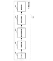
図1の半導体装置100は、アンテナ101、整流回路102、電荷蓄積回路103、定電圧回路104、及び論理回路105によって構成される。
A
なお、ここでは図示しないが、図1においてアンテナ101は、外部通信装置(以下、通信装置という。またリーダライタ、リーダ/ライタ、コントローラ、インテロゲータ、質問器ともいわれる)からの信号の受信、及び通信装置への信号の送信を行う。
Although not shown here, the
なお、図1において、アンテナ101の形状は、特に限定されない。つまり、半導体装置100におけるアンテナ101に適用する信号の伝送方式は、電磁結合方式、電磁誘導方式又はマイクロ波方式等を用いることができる。伝送方式は、実施者が適宜使用用途を考慮して選択すればよく、伝送方式に伴って最適な長さや形状のアンテナを設ければよい。
Note that in FIG. 1, the shape of the
例えば、伝送方式として、電磁結合方式又は電磁誘導方式(例えば、13.56MHz帯)を適用する場合には、電界密度の変化による電磁誘導を利用するため、アンテナとして機能する導電膜を輪状(例えば、ループアンテナ)、らせん状(例えば、スパイラルアンテナ)に形成する。 For example, when an electromagnetic coupling method or an electromagnetic induction method (for example, 13.56 MHz band) is applied as a transmission method, a conductive film functioning as an antenna is formed in a ring shape (for example, an electromagnetic induction due to a change in electric field density). , Loop antenna), and spiral (for example, spiral antenna).
また、伝送方式としてマイクロ波方式(例えば、UHF帯(860〜960MHz帯)、2.45GHz帯等)を適用する場合には、信号の伝送に用いる電波の波長を考慮してアンテナとして機能する導電膜の長さや形状を適宜設定すればよく、アンテナとして機能する導電膜を、線状(例えば、ダイポールアンテナ)、平坦な形状(例えば、パッチアンテナ)等に形成することができる。また、アンテナとして機能する導電膜の形状は線状に限られず、電磁波の波長を考慮して曲線状や蛇行形状またはこれらを組み合わせた形状で設けてもよい。 In addition, when a microwave method (for example, UHF band (860 to 960 MHz band), 2.45 GHz band, or the like) is applied as a transmission method, a conductive function that functions as an antenna in consideration of the wavelength of a radio wave used for signal transmission. The length and shape of the film may be set as appropriate, and the conductive film functioning as an antenna can be formed in a linear shape (for example, a dipole antenna) or a flat shape (for example, a patch antenna). Further, the shape of the conductive film functioning as an antenna is not limited to a linear shape, and may be provided in a curved shape, a meandering shape, or a combination thereof in consideration of the wavelength of electromagnetic waves.
なお、半導体装置と通信装置との通信方式は、単方向通信または双方向通信であって、空間分割多重化方式、偏波面分割多重化方式、周波数分割多重化方式、時分割多重化方式、符号分割多重化方式、直交周波数分割多重化方式のいずれも用いることができる。 The communication method between the semiconductor device and the communication device is unidirectional communication or bidirectional communication, and is a space division multiplexing method, a polarization plane division multiplexing method, a frequency division multiplexing method, a time division multiplexing method, a code Either division multiplexing or orthogonal frequency division multiplexing can be used.
なお、半導体装置と通信装置との搬送波の周波数は、サブミリ波である300GHz以上3THz未満、ミリ波である30GHz以上300GHz未満、マイクロ波である3GHz以上30GHz未満、極超短波である300MHz以上3GHz未満、超短波である30MHz以上300MHz未満、短波である3MHz以上30MHz未満、中波である300kHz以上3MHz未満、長波である30kHz以上300kHz未満、及び超長波である3kHz以上30kHz未満のいずれの周波数も用いることができる。また、半導体装置と通信装置との搬送波の変調方式は、アナログ変調であってもデジタル変調であってもよく、振幅変調、位相変調、周波数変調、及びスペクトラム拡散のいずれであってもよい。望ましくは、振幅変調、または、周波数変調にするとよい。 In addition, the frequency of the carrier wave of the semiconductor device and the communication device is 300 GHz or more and less than 3 THz, which is a submillimeter wave, 30 GHz or more and less than 300 GHz, which is a millimeter wave, 3 GHz or more, but less than 30 GHz, which is a microwave, It is possible to use any frequency of 30 MHz to 300 MHz, which is an ultrashort wave, 3 MHz to less than 30 MHz, which is a short wave, 300 kHz to less than 3 MHz, which is a medium wave, 30 kHz to less than 300 kHz, which is a long wave, it can. Further, the modulation method of the carrier wave between the semiconductor device and the communication device may be analog modulation or digital modulation, and may be any of amplitude modulation, phase modulation, frequency modulation, and spread spectrum. Desirably, amplitude modulation or frequency modulation is used.
次に、図1に示した整流回路102の構成例について図2(A)、図2(B)に示す。整流回路102は、アンテナ101が受信する電波により生成される交流信号を直流信号に変換する回路であればよい。例えば、図2(A)に示すように整流回路200aは、ダイオード201、容量素子202によって整流回路102を構成すればよい。
Next, structural examples of the
なお、図1に示した整流回路102は、半波2倍圧整流回路と呼ばれる回路構成を採用してもよい。例えば、図2(B)に示すように整流回路200bは、容量素子203、ダイオード204、ダイオード205、容量素子206によって、半波2倍圧整流回路を構成すればよい。これに限らず半波4倍圧整流回路や半波6倍圧整流回路や全波整流回路などを用いてもよい。
Note that the
なお、図2(A)及び図2(B)に示す容量素子は2つの端子を用いて電気的な接続が行われている。その場合、容量素子の一方の電極を第1の電極と呼び、他方の電極を第2の電極と呼ぶ。また、図2(A)及び図2(B)に示すダイオードは2つの端子を用いて電気的な接続が行われている。その場合、ダイオードの陽極を第1の電極と呼び、ダイオードの陰極を第2の電極と呼ぶ。 Note that the capacitor shown in FIGS. 2A and 2B is electrically connected using two terminals. In that case, one electrode of the capacitor is referred to as a first electrode, and the other electrode is referred to as a second electrode. In addition, the diodes illustrated in FIGS. 2A and 2B are electrically connected using two terminals. In that case, the anode of the diode is called the first electrode, and the cathode of the diode is called the second electrode.
次に図1に示した定電圧回路104の構成例について図19に示す。図19に示す定電圧回路104は第1の抵抗素子901、第2の抵抗素子902、コンパレータ903、トランジスタ904を有する構成である。コンパレータ903は、基準電圧が非反転入力端子に入力され、論理回路105に接続される側のノードの電圧を第1の抵抗素子901と第2の抵抗素子902とで抵抗分割した電圧が反転入力端子に入力され、これらの電圧値を比較する機能を有する。コンパレータ903の出力端子は、トランジスタ904のゲート端子に接続される。そしてコンパレータ903は、トランジスタ904を介して一定の電圧を出力する機能を奏するものである。
Next, FIG. 19 shows a structural example of the
次に、本発明の特徴点である図1に示す半導体装置が具備する電荷蓄積回路103の構成について詳述する。電荷蓄積回路103は複数の容量素子、及び複数のスイッチを有し、並列に設けられた容量素子が、それぞれスイッチを介して電気的に接続されている。電荷蓄積回路103は、整流回路102より出力される直流信号の電荷をスイッチのオン又はオフを切り替えることにより複数の容量素子に順次蓄積していくことで所望の電圧に短期間に昇圧し、定電圧回路104に安定した電圧を出力する電圧をする回路である。
Next, the configuration of the
図3に電荷蓄積回路103の具体的な回路構成について示し、説明する。図3に示す電荷蓄積回路300は、第1の容量素子301a、第2の容量素子301b、第3の容量素子301c、第4の容量素子301d、スイッチ302a、スイッチ302b、スイッチ302c、及び電荷蓄積制御回路303を有する。図3において、整流回路102は、第1の容量素子301aの第1の電極及びスイッチ302aの一方の端子に電気的に接続される。また、第1の容量素子301aの第1の電極、第2の容量素子301bの第1の電極、第3の容量素子301cの第1の電極、及び第4の容量素子301dの第1の電極は、スイッチ302a、スイッチ302b、及びスイッチ302cを介して、並列に接続されている。また第1の容量素子301aの第2の電極、第2の容量素子301bの第2の電極、第3の容量素子301cの第2の電極、及び第4の容量素子301dの第2の電極は、それぞれグラウンド線に接続されている。また、スイッチ302a、スイッチ302b、及びスイッチ302cは、電荷蓄積制御回路303によって、オンまたはオフが制御される。
FIG. 3 shows a specific circuit configuration of the
なお、図3において、電荷蓄積回路300を構成する容量素子の数が4つ、スイッチの数が3つである場合の例について示した。本発明は、容量素子の数及びスイッチの数が限定されないものであることを付記する。本実施の形態で説明する構成においては、並列に接続された容量素子の一方の電極間に、スイッチを設ける構成であればよい。なお図3において、スイッチ間のノードに接続される容量素子は1つである例について示したが、複数設ける構成でもよい。
Note that FIG. 3 illustrates an example in which the number of capacitive elements included in the
次に電荷蓄積回路103の具体的な動作について図4(A)乃至(C)及び図5(A)乃至(C)を用いて説明する。なお、図4(A)乃至(C)及び図5(A)乃至(C)に示す電荷蓄積回路400は、第1の容量素子401a、第2の容量素子401b、第3の容量素子401c、スイッチ402a、及びスイッチ402bを有する。なお、図4(A)乃至(C)及び図5(A)乃至(C)では、各スイッチのオン又はオフの動作について説明するものであるため、電荷蓄積制御回路については図示しない。また、図4(A)乃至(C)及び図5(A)乃至(C)において、整流回路102から入力される直流信号の電荷をQ、定電圧回路104に出力される電圧がV0,V1,V2と段階的に変化する例について説明する。なお、前述の定電圧回路104に出力される電圧はV0<V1<V2の関係を有するものとする。そして直流信号は、第1の容量素子401aの第1の電極及びスイッチ402aの一方の端子に入力される。また、第1の容量素子401aの第1の電極、第2の容量素子401bの第1の電極、及び第3の容量素子401cの第1の電極は、スイッチ402a及びスイッチ402bを介して、並列に接続されている。また第1の容量素子401aの第2の電極、第2の容量素子401bの第2の電極、及び第3の容量素子401cの第2の電極は、それぞれグラウンド線に接続されている。また、スイッチ402a、及びスイッチ402bは、電荷蓄積制御回路(図示せず)によって、オンまたはオフが制御される。なお、図4(A)に符号を付し、図4(B)乃至(C)及び図5(A)乃至(C)については、省略している。また図4(A)乃至(C)及び図5(A)乃至(C)で説明する第1の容量素子401aの静電容量をC1、第2の容量素子401bの静電容量をC2、第3の容量素子401cの静電容量をC3とする。なお、静電容量C1、静電容量C2、及び静電容量C3は、同じ静電容量でも良いし、異なっていてもよい。
Next, a specific operation of the
なお本明細書で説明する定電圧回路104に出力される電圧とは、グラウンド電位を基準電位とした場合の、電位差に相当する。そのため、電圧V0乃至V2のことを電位V0乃至V2と呼ぶこともある。
Note that the voltage output to the
図4(A)の状態について説明する。電荷蓄積回路400には、整流回路102から出力される直流信号の電荷Qが蓄積される。電荷蓄積回路400は、初期状態ではスイッチはオフ、すなわちスイッチ402a及びスイッチ402bはオフになっており、電荷Qは静電容量C1である第1の容量素子401aに蓄積されていく。このとき、静電容量C1である第1の容量素子401aに電荷Qが蓄積されることにより、静電容量C、電荷Q、及び電圧Vの関係式:Q=CVより、Q/C1=V0(V0は定電圧回路104に出力する所望の電圧)を得ることができる。なお、第1の容量素子401aの静電容量C1は、蓄積される電荷Qによって短期間に電圧V1が得られるよう予め小さく設計することが望ましい。
The state in FIG. 4A will be described. The charge storage circuit 400 stores the charge Q of the DC signal output from the
なお、本明細書でいう電荷Qとは、整流回路102で得られる直流信号の電圧によって、電荷蓄積回路400に供給される電荷のことをいう。そして、電荷蓄積回路400では、電荷を蓄積するための静電容量の値が小さいほど、短期間に所望の電圧を得ることができる。なお、説明のため本実施の形態において、電荷蓄積回路400に供給される電荷Qは、図4(B)乃至(C)の状態となる期間ごとに供給される電荷の総数であるものとする。
Note that the charge Q in this specification refers to the charge supplied to the charge storage circuit 400 by the voltage of the DC signal obtained by the
次に図4(B)の状態について説明する。電荷蓄積回路400には、整流回路102から出力される直流信号の電荷Qが図4(A)の状態に引き続き供給されている。このとき、定電圧回路104に出力するための所望の電圧V0が既に得られているものの、電荷を蓄積するための第1の容量素子401aでは、整流回路102から出力される直流信号の電圧に依存して、蓄積できる電荷が飽和してしまう。この状態のとき、スイッチ402aをオンにすることにより、電荷を蓄積することのできる容量素子を第1の容量素子401a及び第2の容量素子401bと増やすことで、アンテナ101で受信した電力を、電荷として容量素子に蓄積することができる。図4(B)の状態のとき、電荷を蓄積するための静電容量は第1の容量素子401a及び第2の容量素子401bが有する静電容量を併せた静電容量(C1+C2)となる。電荷Qは図4(A)の状態で蓄積された分の電荷Qと、順次電荷蓄積回路400に入力される電荷Qと併せて2Qとなる。そして、静電容量、電荷、及び電圧の関係式により、2Q/(C1+C2)=V1を得ることができる。なお静電容量C2は、静電容量C1に比べて小さいものであることが望ましい、静電容量C2を静電容量C1に比べて小さく設けることにより、スイッチ402aがオンになる際の電圧V0から電圧V1に変化する際の電圧の変動幅を小さくすることができ、安定した電圧を定電圧回路104に供給することができる。
Next, the state of FIG. 4B will be described. The charge storage circuit 400 is continuously supplied with the charge Q of the DC signal output from the
次に図4(C)の状態について説明する。電荷蓄積回路400には、整流回路102から出力される直流信号の電荷Qが、図4(A)、図4(B)の状態に引き続き供給されている。このとき、定電圧回路104に出力するためのV0が既に得られているものの、電荷を蓄積するための第1の容量素子401a及び第2の容量素子401bでは、整流回路102から出力される直流信号の電圧に依存して、蓄積できる電荷が飽和してしまう。この状態のとき、スイッチ402aと併せてスイッチ402bをオンにすることにより、電荷を蓄積することのできる容量素子を第1の容量素子401a、第2の容量素子401b、第3の容量素子401cと増やすことにより、アンテナ101で受信した電力を、電荷として容量素子に蓄積することができる。図4(C)の状態のとき、電荷を蓄積するための静電容量は第1の容量素子401a、第2の容量素子401b、及び第3の容量素子401cが有する静電容量を併せた静電容量(C1+C2+C3)となる。電荷Qは図4(B)の状態で蓄積された分の電荷2Qと、順次電荷蓄積回路400に入力される電荷Qと併せて3Qとなる。そして、静電容量、電荷、及び電圧の関係式により、3Q/(C1+C2+C3)=V2を得ることができる。なお静電容量C3は、静電容量(C1+C2)に比べて小さいものであることが望ましい、静電容量C3を静電容量(C1+C2)に比べて小さく設けることにより、スイッチ402bがオンになる際の電圧V1から電圧V2に変化する際の電圧の変動幅を小さくすることができ、安定した電圧を定電圧回路104に供給することができる。
Next, the state of FIG. 4C will be described. The charge storage circuit 400 is continuously supplied with the charge Q of the DC signal output from the
以上図4(A)乃至図4(C)では、電荷蓄積回路400の電荷の蓄積方法について示した。図4(A)乃至図4(C)に示す構成は一例であり、容量素子及びスイッチの数を増やして電荷を蓄積することが出来る静電容量を増やす構成としてもよい。また、スイッチのオンまたはオフについては、図4(A)乃至図4(C)で示した順に限定されるものではなく、例えばスイッチ402aとスイッチ402bを同時にオンして電荷を蓄積するための静電容量を可変する構成としてもよい。
4A to 4C, the charge accumulation method of the charge accumulation circuit 400 has been described. The structures illustrated in FIGS. 4A to 4C are examples, and the number of capacitors and switches may be increased to increase the capacitance that can store charges. Further, on / off of the switch is not limited to the order shown in FIGS. 4A to 4C. For example, static electricity for accumulating charges by simultaneously turning on the
次に、電荷蓄積回路400に蓄積された電荷の放出に関する動作について図5(A)乃至図5(C)を用いて説明する。 Next, an operation related to the discharge of the charge accumulated in the charge accumulation circuit 400 will be described with reference to FIGS.
図5(A)の状態について説明する。電荷蓄積回路400は、整流回路102から出力される直流信号の電圧による電荷の供給が行われない期間、定電圧回路104への安定した電圧の出力を行うため、複数の容量素子に保持された電荷を放出して、安定した電圧を定電圧回路104に出力する。複数の容量素子に蓄積された電荷の放出は、図5(A)に示すように、スイッチ402a及びスイッチ402bが共にオンの状態から、図5(B)に示すように、スイッチ402aをオン及びスイッチ402bをオフの状態を経て、図5(C)に示すように、スイッチ402a及びスイッチ402bが共にオフの状態とする。そして、図5(A)乃至図5(C)に説明したように電荷蓄積回路400は、複数の容量素子である第1の容量素子、第2の容量素子、及び第3の容量素子からの電荷の放出を行うことができる。
The state of FIG. 5A will be described. The charge storage circuit 400 is held by a plurality of capacitors in order to output a stable voltage to the
ここで、図3で示したスイッチ302a乃至スイッチ302c、及び図4(B)乃至(C)及び図5(A)乃至(C)で説明したスイッチ402a及びスイッチ402bの具体的な構成について図6を用いて説明する。電荷の蓄積時及び放出時の電荷蓄積回路の動作を加えて説明するため、図6では、図4(B)乃至(C)及び図5(A)乃至(C)で説明したスイッチ402aの構成を具体的に説明するものとする。
Here, specific configurations of the
図6に示すスイッチ402aは第1の抵抗素子601、第2の抵抗素子602、コンパレータ603、トランジスタ604、ダイオード605を有する構成である。コンパレータ603は、図3で説明した電荷蓄積制御回路303からの参照電圧(図6中のVref)が反転入力端子に入力され、第1の容量素子401aの第1の電極の電圧を第1の抵抗素子601と第2の抵抗素子602とで抵抗分割した電圧が非反転入力端子に入力され、これらの電圧値を比較する機能を有する。コンパレータ603の出力端子は、トランジスタ604のゲート端子に接続される。そしてコンパレータ603は、第1の容量素子401aの第1の電極の電圧がV0より大きい場合にトランジスタ604をオンにし、第1の容量素子401aの第1の電極と第2の容量素子401bの第1の電極を電気的に接続させるスイッチとしての機能を奏するものである。そのため図3で説明した電荷蓄積制御回路303により、参照電圧を制御することで、複数の容量素子に順次電荷を蓄積するためのスイッチのオン又はオフの制御を行うことができる。ダイオード605は第1の電極が第2の容量素子401bの第1の電極に接続され、ダイオード605の第2の電極が第1の容量素子401aの第1の電極に接続されるように設けられる。
A
なお、電荷蓄積時において、第1の容量素子401aと第2の容量素子401bへの電荷の蓄積は、第1の容量素子401aの方が一定の電圧に達するまでは第2の容量素子401bの第1の電極に電荷の蓄積を行われないようにすることで所望の電圧を短期間に得ることができる。また電荷放出時において、第1の容量素子401aと第2の容量素子401bからの電荷の放出は、第1の容量素子401aの電圧が降下した場合に、第2の容量素子401bに蓄積されている電荷を第1の容量素子401a側に供給して第1の容量素子401aの第1の電極に電荷を補給するように行われるようにすることで、電荷の放出を効率よく行い、且つ所望の電圧を効率よく得ることができる。本実施の形態で説明する図6の構成において、ダイオード605は、電荷蓄積時には、第1の容量素子401aから第2の容量素子401bへ電荷の漏電を防ぐものであり、電荷放出時には、第1の容量素子401aが電荷の放出により電圧降下した際に、第2の容量素子401b側より電荷の補給を行うようにするものである。
Note that during the charge accumulation, the charge accumulation in the first capacitor element 401a and the second capacitor element 401b is performed until the first capacitor element 401a reaches a certain voltage until the first capacitor element 401a reaches a certain voltage. A desired voltage can be obtained in a short period of time by preventing charge accumulation in the first electrode. At the time of charge discharge, charge discharge from the first capacitor element 401a and the second capacitor element 401b is accumulated in the second capacitor element 401b when the voltage of the first capacitor element 401a drops. The charge is efficiently discharged and the charge is supplied to the first electrode of the first capacitor element 401a by supplying the charged charge to the first capacitor element 401a side. Can be obtained efficiently. In the configuration of FIG. 6 described in this embodiment, the
なお、本実施の形態においては、スイッチ402aの構成について詳細に説明したが、他のスイッチのおいても参照電圧を異ならせることで同様の機能を奏するものであり、ここでは説明を省略する。
In the present embodiment, the configuration of the
次に、電荷蓄積回路における本発明の特徴である、分割して設けた容量素子間をスイッチで切り替えて静電容量を可変にし、電荷の蓄積を行う利点について図7を用いて説明する。図7では、具体的な説明をするため、上記図4(A)乃至(C)及び図5(A)乃至(C)で説明した電荷蓄積回路が具備する第1の容量素子乃至第3の容量素子の静電容量C1乃至C3を用いた電荷蓄積時の電圧の変化について述べる。 Next, the advantage of performing charge accumulation by switching capacitance between divided capacitive elements, which is a feature of the present invention in the charge storage circuit, by making the capacitance variable will be described with reference to FIG. 7A to 7C, the first capacitor element to the third capacitor included in the charge storage circuit described in FIGS. 4A to 5C and FIGS. A change in voltage during charge accumulation using the capacitances C1 to C3 of the capacitive element will be described.
図7に示す図は、電荷蓄積回路を構成する容量素子の静電容量(図中では単に容量と呼ぶ)が(C1+C2+C3)である場合、電荷蓄積回路を構成する容量素子の静電容量が(C1)、及び電荷蓄積回路を構成する容量素子の静電容量が(C1)から(C1+C2)、(C1+C2)から(C1+C2+C3)と可変させた場合の電荷の蓄積量と定電圧回路に出力される電圧の相関について示したものである。なお、容量素子の静電容量の大きさは、(C1)<(C1+C2)<(C1+C2+C3)となる。 In the diagram shown in FIG. 7, when the capacitance of the capacitive element forming the charge storage circuit (referred to simply as “capacitance” in the drawing) is (C1 + C2 + C3), the capacitance of the capacitive element forming the charge storage circuit is ( C1), and the amount of charge accumulated when the capacitance of the capacitive element constituting the charge storage circuit is varied from (C1) to (C1 + C2) and (C1 + C2) to (C1 + C2 + C3) and is output to the constant voltage circuit It shows the correlation of voltage. Note that the capacitance of the capacitive element is (C1) <(C1 + C2) <(C1 + C2 + C3).
まず図7に示すグラフにおいて、静電容量が(C1)である場合、及び静電容量が(C1+C2+C3)である場合の電荷の蓄積量と定電圧回路に出力される電圧の相関について説明する。なお、電荷蓄積回路に蓄積される電荷の量は、前段の整流回路から出力される直流信号の電圧に依存するものであるため、図7の説明では、整流回路から出力される直流信号の電圧が一定である場合について説明を行う。 First, in the graph shown in FIG. 7, the correlation between the charge accumulation amount and the voltage output to the constant voltage circuit when the capacitance is (C1) and when the capacitance is (C1 + C2 + C3) will be described. Note that the amount of charge accumulated in the charge accumulation circuit depends on the voltage of the DC signal output from the preceding rectifier circuit. Therefore, in the description of FIG. 7, the voltage of the DC signal output from the rectifier circuit is described. The case where is constant will be described.
図7に示すグラフにおいて、静電容量が(C1)である場合、電荷の蓄積に対する電圧の変化量は、静電容量C、電荷Q、及び電圧Vの関係式:V=Q/C により電荷の蓄積に対する電圧の変化量は大きいものの、蓄積することのできる電荷量は少ない。一方、静電容量が(C1+C2+C3)である場合、静電容量C、電荷Q、及び電圧Vの関係式:V=Q/C により、電荷の蓄積に対する電圧の変化量は小さいものの、蓄積することのできる電荷量は多い。 In the graph shown in FIG. 7, when the capacitance is (C1), the amount of change in voltage with respect to charge accumulation is expressed by the relational expression of capacitance C, charge Q, and voltage V: V = Q / C Although the amount of change in voltage with respect to the accumulation of is large, the amount of charge that can be accumulated is small. On the other hand, when the capacitance is (C1 + C2 + C3), the relationship between the capacitance C, the charge Q, and the voltage V is V = Q / C. The amount of charge that can be produced is large.
次に、静電容量が(C1)から(C1+C2)、(C1+C2)から(C1+C2+C3)と可変させた場合の電荷の蓄積量と定電圧回路に出力される電圧の相関について説明する。静電容量が電荷の蓄積開始時に(C1)である場合、静電容量C、電荷Q、及び電圧Vの関係式:V=Q/C により、電荷の蓄積に対する電圧の変化量は大きいものの、蓄積することのできる電荷量は少ない。しかし本実施の形態の構成では、電荷の蓄積により、所望の電圧まで短期間に達した後に静電容量が(C1)から(C1+C2)、(C1+C2)から(C1+C2+C3)と可変することができる。そのため、電荷の蓄積により、所望の電圧に達した後は、蓄積することのできる電荷を増やすことができる。そのため、本実施の形態で説明した電荷蓄積回路を具備する半導体装置では、エネルギーを蓄積していない初期状態において、電荷蓄積回路の静電容量が小さくなるようにスイッチを制御することで、短期間に所望の電圧を生成することができる。そして、所望の電源電圧が得られた後、電荷蓄積回路の静電容量を大きくなるようにスイッチを制御することで、入力される電荷を効率よく蓄積することができ、且つ安定した電圧を定電圧回路に供給することができる。 Next, the correlation between the charge accumulation amount and the voltage output to the constant voltage circuit when the capacitance is varied from (C1) to (C1 + C2) and (C1 + C2) to (C1 + C2 + C3) will be described. When the capacitance is (C1) at the start of charge accumulation, the relationship between the capacitance C, the charge Q, and the voltage V: V = Q / C The amount of charge that can be stored is small. However, in the configuration of the present embodiment, the electrostatic capacity can be changed from (C1) to (C1 + C2) and (C1 + C2) to (C1 + C2 + C3) after reaching a desired voltage in a short time due to the accumulation of electric charges. Therefore, the charge that can be accumulated can be increased after reaching a desired voltage due to the accumulation of the charge. Therefore, in the semiconductor device including the charge storage circuit described in this embodiment, in an initial state where energy is not stored, the switch is controlled so that the capacitance of the charge storage circuit becomes small, so that a short period of time can be obtained. A desired voltage can be generated. Then, after the desired power supply voltage is obtained, by controlling the switch so as to increase the capacitance of the charge storage circuit, the input charge can be stored efficiently and a stable voltage can be determined. The voltage circuit can be supplied.
なお、本実施の形態は、本明細書の実施の形態の技術的要素と組み合わせて行うことができる。 Note that this embodiment mode can be implemented in combination with the technical elements of the embodiment modes in this specification.
(実施の形態2)
本実施の形態では、上記実施の形態で説明した電荷蓄積回路を具備する半導体装置(RFIDタグ、IDチップ、ICタグ、IDタグ、RFタグ、無線タグ、電子タグ、トランスポンダともいわれる)の構成について説明する。
(Embodiment 2)
In this embodiment, a structure of a semiconductor device (also referred to as an RFID tag, an ID chip, an IC tag, an ID tag, an RF tag, a wireless tag, an electronic tag, or a transponder) including the charge accumulation circuit described in the above embodiment is described. explain.
図8における半導体装置800は、一例として、アンテナ801、整流回路802、電荷蓄積回路803、定電圧回路804、復調回路805、変調回路806、論理回路807によって構成されている。また、論理回路807はコントローラ808、CPU809(Central Processing Unit)、ROM810(Read Only Memory)、RAM811(Random Access Memory)によって構成されている。論理回路807は、CPU809などの論理回路、ワーク領域としてのRAM811として揮発性メモリ(代表的にはSRAM)、CPU809のプログラムを格納する書き込み可能なROM810として不揮発性メモリ(代表的にはEEPROM)によって構成され、コントローラ808により各ブロック間のデータの読み出しまたは書き込みを制御するものであればよい。
The
なお、半導体装置800における電荷蓄積回路803は、上記実施の形態で説明した構成を取り得る。すなわち、エネルギーを蓄積していない初期状態において、電荷蓄積回路の静電容量が小さくなるようにスイッチを制御することで、短期間に所望の電圧を生成することができる。そして、所望の電源電圧が得られた後、電荷蓄積回路の静電容量を大きくなるようにスイッチを制御することで、入力される電荷を効率よく蓄積することができ、且つ安定した電圧を定電圧回路に供給することができるものである。
Note that the
図8において、アンテナ801で外部の通信装置より受信した信号が整流回路802に入力される。整流回路802からの出力信号は復調回路805、及び電荷蓄積回路803に入力される。復調回路805からの信号は論理回路807に入力され、半導体装置の固有情報に関する情報が変調回路806に出力される。そして変調回路806からの出力信号はアンテナ801に出力され、半導体装置外部の通信装置に信号が出力される。また電荷蓄積回路803からは定電圧回路804で一定の電圧を出力するための電圧が定電圧回路804に供給される。そして定電圧回路804からは、半導体装置の各回路を動作するための電源電圧が供給される。
In FIG. 8, a signal received from an external communication device by the
なお、通信装置と半導体装置の間の信号の伝送方式は、搬送波の波長によって電磁結合方式、電磁誘導方式、マイクロ波方式など様々な種類に分類することができる。なお、半導体装置と通信装置との無線信号の送受信を長距離間で行う場合には、マイクロ波方式を選択することが望ましい。 Note that signal transmission methods between a communication device and a semiconductor device can be classified into various types such as an electromagnetic coupling method, an electromagnetic induction method, and a microwave method depending on the wavelength of a carrier wave. Note that when a radio signal is transmitted and received between a semiconductor device and a communication device over a long distance, it is desirable to select a microwave method.
なお、本実施の形態は、本明細書の実施の形態の技術的要素と組み合わせて行うことができる。 Note that this embodiment mode can be implemented in combination with the technical elements of the embodiment modes in this specification.
(実施の形態3)
本実施の形態では、上記実施の形態で述べた半導体装置を構成するトランジスタの作製例について説明する。本実施の形態では特に、絶縁基板上に形成された半導体膜により作成したトランジスタを具備する半導体装置とする形態について説明する。
(Embodiment 3)
In this embodiment, an example of manufacturing a transistor included in the semiconductor device described in the above embodiment will be described. In this embodiment mode, a mode in which a semiconductor device including a transistor formed using a semiconductor film formed over an insulating substrate is particularly described.
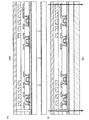
基板1901の一表面に剥離層1902を形成し、続けて下地となる絶縁膜1903および非晶質半導体膜1904(例えば非晶質珪素を含む膜)を形成する(図9(A))。剥離層1902、絶縁膜1903および非晶質半導体膜1904は、連続して形成することができる。連続して形成することにより、大気に曝されないため不純物の混入を防ぐことができる。
A
基板1901は、ガラス基板、石英基板、金属基板やステンレス基板、本工程の処理温度に耐えうる耐熱性があるプラスチック基板等を用いるとよい。このような基板であれば、その面積や形状に大きな制限はないため、例えば、1辺が1メートル以上であって、矩形状のものを用いれば、生産性を格段に向上させることができる。このような利点は、円形のシリコン基板を用いる場合と比較すると、大きな優位点である。従って、シリコン基板と比較して集積回路部やアンテナを大きく形成した場合であっても、低コスト化を実現することができる。
As the
なお、本工程では、剥離層1902を基板1901の全面に設けているが、必要に応じて、基板1901の全面に剥離層を設けた後に、フォトリソグラフィ法及びエッチングにより剥離層1902を選択的に設けてもよい。また、基板1901に接するように剥離層1902を形成しているが、必要に応じて、基板1901に接するように酸化珪素(SiOx)膜、酸化窒化珪素(SiOxNy)(x>y)膜、窒化珪素(SiNx)膜、窒化酸化珪素(SiNxOy)(x>y)膜等の絶縁膜を形成し、当該絶縁膜に接するように剥離層1902を形成してもよい。
Note that although the
剥離層1902は、金属膜や金属膜と金属酸化膜の積層構造等を用いることができる。金属膜としては、タングステン(W)、モリブデン(Mo)、チタン(Ti)、タンタル(Ta)、ニオブ(Nb)、ニッケル(Ni)、コバルト(Co)、ジルコニウム(Zr)、亜鉛(Zn)、ルテニウム(Ru)、ロジウム(Rh)、パラジウム(Pd)、オスミウム(Os)、イリジウム(Ir)から選択された元素または前記元素を主成分とする合金材料若しくは化合物材料からなる膜を単層又は積層して形成する。また、これらの材料は、スパッタリング法やプラズマCVD法等の各種CVD法等を用いて形成することができる。金属膜と金属酸化膜の積層構造としては、上述した金属膜を形成した後に、酸素雰囲気下またはN2O雰囲気下におけるプラズマ処理、酸素雰囲気下またはN2O雰囲気下における加熱処理を行うことによって、金属膜表面に当該金属膜の酸化物または酸化窒化物を設けることができる。また、金属膜を形成した後に、オゾン水等の酸化力の強い溶液で表面を処理することにより、金属膜表面に当該金属膜の酸化物又は酸化窒化物を設けることができる。
For the
絶縁膜1903は、スパッタリング法やプラズマCVD法等により、珪素の酸化物または珪素の窒化物を含む膜を、単層又は積層で形成する。下地となる絶縁膜が2層構造の場合、例えば、1層目として窒化酸化珪素膜を形成し、2層目として酸化窒化珪素膜を形成するとよい。下地となる絶縁膜が3層構造の場合、1層目の絶縁膜として酸化珪素膜を形成し、2層目の絶縁膜として窒化酸化珪素膜を形成し、3層目の絶縁膜として酸化窒化珪素膜を形成するとよい。または、1層目の絶縁膜として酸化窒化珪素膜を形成し、2層目の絶縁膜として窒化酸化珪素膜を形成し、3層目の絶縁膜として酸化窒化珪素膜を形成するとよい。下地となる絶縁膜は、基板1901からの不純物の侵入を防止するブロッキング膜として機能する。
The insulating
半導体膜1904は、スパッタリング法、LPCVD法、プラズマCVD法等により、25〜200nm(好ましくは30〜150nm)の厚さで形成する。半導体膜1904としては、例えば、非晶質珪素膜を形成すればよい。
The
次に、非晶質の半導体膜1904にレーザー光を照射して結晶化を行う。なお、レーザー光の照射と、RTA又はファーネスアニール炉を用いる熱結晶化法、結晶化を助長する金属元素を用いる熱結晶化法とを組み合わせた方法等により非晶質の半導体膜1904の結晶化を行ってもよい。その後、得られた結晶質半導体膜を所望の形状にエッチングして、半導体膜1904a〜1904dを形成し、当該半導体膜1904a〜1904dを覆うようにゲート絶縁膜1905を形成する(図9(B))。
Next, crystallization is performed by irradiating the
半導体膜1904a〜1904dの作製工程の一例を以下に簡単に説明すると、まず、プラズマCVD法を用いて、膜厚50〜60nmの非晶質半導体膜(例えば、非晶質珪素膜)を形成する。次に、結晶化を助長する金属元素であるニッケルを含む溶液を非晶質半導体膜上に保持させた後、非晶質半導体膜に脱水素化の処理(500℃、1時間)と、熱結晶化の処理(550℃、4時間)を行って結晶質半導体膜を形成する。その後、レーザー発振器からレーザー光を照射し、フォトリソグラフィ法及びエッチングを用いることよって半導体膜1904a〜1904dを形成する。なお、結晶化を助長する金属元素を用いる熱結晶化を行わずに、レーザー光の照射だけで非晶質半導体膜の結晶化を行ってもよい。
An example of a manufacturing process of the
レーザー発振器としては、連続発振型のレーザー(CWレーザー)やパルス発振型のレーザー(パルスレーザー)を用いることができる。ここで用いることができるレーザービームは、Arレーザー、Krレーザー、エキシマレーザーなどの気体レーザー、単結晶のYAG、YVO4、フォルステライト(Mg2SiO4)、YAlO3、GdVO4、若しくは多結晶(セラミック)のYAG、Y2O3、YVO4、YAlO3、GdVO4に、ドーパントとしてNd、Yb、Cr、Ti、Ho、Er、Tm、Taのうち1種または複数種添加されているものを媒質とするレーザー、ガラスレーザー、ルビーレーザー、アレキサンドライトレーザー、Ti:サファイアレーザー、銅蒸気レーザーまたは金蒸気レーザーのうち一種または複数種から発振されるものを用いることができる。このようなレーザービームの基本波、及びこれらの基本波の第2高調波から第4高調波のレーザービームを照射することで、大粒径の結晶を得ることができる。例えば、Nd:YVO4レーザー(基本波1064nm)の第2高調波(532nm)や第3高調波(355nm)を用いることができる。このときレーザーのパワー密度は0.01〜100MW/cm2程度(好ましくは0.1〜10MW/cm2)が必要である。そして、走査速度を10〜2000cm/sec程度として照射する。なお、単結晶のYAG、YVO4、フォルステライト(Mg2SiO4)、YAlO3、GdVO4、若しくは多結晶(セラミック)のYAG、Y2O3、YVO4、YAlO3、GdVO4に、ドーパントとしてNd、Yb、Cr、Ti、Ho、Er、Tm、Taのうち1種または複数種添加されているものを媒質とするレーザー、Arイオンレーザー、またはTi:サファイアレーザーは、連続発振をさせることが可能であり、Qスイッチ動作やモード同期などを行うことによって10MHz以上の発振周波数でパルス発振をさせることも可能である。10MHz以上の発振周波数でレーザービームを発振させると、半導体膜がレーザーによって溶融してから固化するまでの間に、次のパルスが半導体膜に照射される。従って、発振周波数が低いパルスレーザーを用いる場合と異なり、半導体膜中において固液界面を連続的に移動させることができるため、走査方向に向かって連続的に成長した結晶粒を得ることができる。 As the laser oscillator, a continuous wave laser (CW laser) or a pulsed laser (pulse laser) can be used. The laser beam that can be used here is a gas laser such as Ar laser, Kr laser, or excimer laser, single crystal YAG, YVO 4 , forsterite (Mg 2 SiO 4 ), YAlO 3 , GdVO 4 , or polycrystalline ( (Ceramics) YAG, Y 2 O 3 , YVO 4 , YAlO 3 , GdVO 4 with one or more of Nd, Yb, Cr, Ti, Ho, Er, Tm, Ta added as dopants Lasers oscillated from one or more of laser, glass laser, ruby laser, alexandrite laser, Ti: sapphire laser, copper vapor laser or gold vapor laser as a medium can be used. By irradiating the fundamental wave of such a laser beam and the second to fourth harmonics of these fundamental waves, a crystal having a large grain size can be obtained. For example, the second harmonic (532 nm) or the third harmonic (355 nm) of an Nd: YVO 4 laser (fundamental wave 1064 nm) can be used. In this case, a laser power density is about 0.01 to 100 MW / cm 2 (preferably 0.1 to 10 MW / cm 2) is required. Then, irradiation is performed at a scanning speed of about 10 to 2000 cm / sec. Note that single crystal YAG, YVO 4 , forsterite (Mg 2 SiO 4 ), YAlO 3 , GdVO 4 , or polycrystalline (ceramic) YAG, Y 2 O 3 , YVO 4 , YAlO 3 , GdVO 4 , dopants Nd, Yb, Cr, Ti, Ho, Er, Tm, Ta as a medium, a laser, Ar ion laser, or Ti: sapphire laser with one or more added as a medium should be continuously oscillated It is also possible to perform pulse oscillation at an oscillation frequency of 10 MHz or more by performing Q switch operation, mode synchronization, or the like. When a laser beam is oscillated at an oscillation frequency of 10 MHz or higher, the semiconductor film is irradiated with the next pulse during the period from when the semiconductor film is melted by the laser to solidification. Therefore, unlike the case of using a pulse laser having a low oscillation frequency, the solid-liquid interface can be continuously moved in the semiconductor film, so that crystal grains continuously grown in the scanning direction can be obtained.
次に、半導体膜1904a〜半導体膜1904dを覆うゲート絶縁膜1905を形成する。ゲート絶縁膜1905は、CVD法やスパッタリング法等により、珪素の酸化物又は珪素の窒化物を含む膜を、単層又は積層して形成する。具体的には、酸化珪素膜、酸化窒化珪素膜、窒化酸化珪素膜を、単層又は積層して形成する。
Next, a
また、ゲート絶縁膜1905は、半導体膜1904a〜半導体膜1904dに対し高密度プラズマ処理を行い、表面を酸化又は窒化することで形成しても良い。例えば、He、Ar、Kr、Xeなどの希ガスと、酸素、酸化窒素(NO2)、アンモニア、窒素、水素などの混合ガスを導入したプラズマ処理で形成する。この場合のプラズマの励起は、マイクロ波の導入により行うと、低電子温度で高密度のプラズマを生成することができる。この高密度プラズマで生成された酸素ラジカル(OHラジカルを含む場合もある)や窒素ラジカル(NHラジカルを含む場合もある)によって、半導体膜の表面を酸化又は窒化することができる。
The
このような高密度プラズマを用いた処理により、1〜20nm、代表的には5〜10nmの絶縁膜が半導体膜に形成される。この場合の反応は、固相反応であるため、当該絶縁膜と半導体膜との界面準位密度はきわめて低くすることができる。このような、高密度プラズマ処理は、半導体膜(結晶性シリコン、或いは多結晶シリコン)を直接酸化(若しくは窒化)するため、形成される絶縁膜の厚さは理想的には、ばらつきをきわめて小さくすることができる。加えて、結晶性シリコンの結晶粒界でも酸化が強くされることがないため、非常に好ましい状態となる。すなわち、ここで示す高密度プラズマ処理で半導体膜の表面を固相酸化することにより、結晶粒界において異常に酸化反応をさせることなく、均一性が良く、界面準位密度が低い絶縁膜を形成することができる。 By such treatment using high-density plasma, an insulating film with a thickness of 1 to 20 nm, typically 5 to 10 nm, is formed over the semiconductor film. Since the reaction in this case is a solid-phase reaction, the interface state density between the insulating film and the semiconductor film can be extremely low. Such high-density plasma treatment directly oxidizes (or nitrides) a semiconductor film (crystalline silicon or polycrystalline silicon), so that the thickness of the formed insulating film ideally has extremely small variation. can do. In addition, since oxidation is not strengthened even at the crystal grain boundaries of crystalline silicon, a very favorable state is obtained. That is, the surface of the semiconductor film is solid-phase oxidized by the high-density plasma treatment shown here, thereby forming an insulating film with good uniformity and low interface state density without causing an abnormal oxidation reaction at the grain boundaries. can do.
ゲート絶縁膜1905は、高密度プラズマ処理によって形成される絶縁膜のみを用いても良いし、それに加えてプラズマや熱反応を利用したCVD法で酸化シリコン、酸窒化シリコン、窒化シリコンなどの絶縁膜を堆積し、積層させても良い。いずれにしても、高密度プラズマで形成した絶縁膜をゲート絶縁膜の一部又は全部に含んで形成されるトランジスタは、特性のばらつきを小さくすることができる。
As the
また、半導体膜に対し、連続発振レーザー光若しくは10MHz以上の周波数で発振するレーザー光を照射しながら一方向に走査して結晶化させて得られた半導体膜1904a〜1904dは、そのレーザー光の走査方向に結晶が成長する特性がある。その走査方向をチャネル長方向(チャネル形成領域が形成されたときにキャリアが流れる方向)に合わせてトランジスタを配置し、上記ゲート絶縁層を組み合わせることで、特性ばらつきが小さく、しかも電界効果移動度が高い薄膜トランジスタ(TFT)を得ることができる。
In addition, the
次に、ゲート絶縁膜1905上に、第1の導電膜と第2の導電膜とを積層して形成する。ここでは、第1の導電膜は、プラズマCVD法やスパッタ法等により、20〜100nmの厚さで形成する。第2の導電膜は、100〜400nmの厚さで形成する。第1の導電膜と第2の導電膜は、タンタル(Ta)、タングステン(W)、チタン(Ti)、モリブデン(Mo)、アルミニウム(Al)、銅(Cu)、クロム(Cr)、ニオブ(Nb)等から選択された元素又はこれらの元素を主成分とする合金材料若しくは化合物材料で形成する。または、リン等の不純物元素をドーピングした多結晶珪素に代表される半導体材料により形成する。第1の導電膜と第2の導電膜の組み合わせの例を挙げると、窒化タンタル膜とタングステン膜、窒化タングステン膜とタングステン膜、窒化モリブデン膜とモリブデン膜等が挙げられる。タングステンや窒化タンタルは、耐熱性が高いため、第1の導電膜と第2の導電膜を形成した後に、熱活性化を目的とした加熱処理を行うことができる。また、2層構造ではなく、3層構造の場合は、モリブデン膜とアルミニウム膜とモリブデン膜の積層構造を採用するとよい。
Next, a first conductive film and a second conductive film are stacked over the
次に、フォトリソグラフィ法を用いてレジストからなるマスクを形成し、ゲート電極とゲート配線を形成するためのエッチング処理を行って、半導体膜1904a〜1904dの上方にゲート電極1907を形成する。
Next, a resist mask is formed by photolithography, and an etching process for forming a gate electrode and a gate wiring is performed, so that a
次に、フォトリソグラフィ法により、レジストからなるマスクを形成して、半導体膜1904a〜1904dに、イオンドープ法またはイオン注入法により、n型を付与する不純物元素を低濃度に添加する。n型を付与する不純物元素は、15族に属する元素を用いれば良く、例えばリン(P)、砒素(As)を用いる。
Next, a resist mask is formed by photolithography, and an impurity element imparting n-type conductivity is added to the
次に、ゲート絶縁膜1905とゲート電極1907を覆うように、絶縁膜を形成する。絶縁膜は、プラズマCVD法やスパッタ法等により、珪素、珪素の酸化物又は珪素の窒化物の無機材料を含む膜や、有機樹脂などの有機材料を含む膜を、単層又は積層して形成する。次に、絶縁膜を、垂直方向を主体とした異方性エッチングにより選択的にエッチングして、ゲート電極1907の側面に接する絶縁膜1908(サイドウォールともよばれる)を形成する。絶縁膜1908は、後にLDD(Lightly Doped drain)領域を形成する際のドーピング用のマスクとして用いる。
Next, an insulating film is formed so as to cover the
次に、フォトリソグラフィ法により形成したレジストからなるマスクと、ゲート電極1907および絶縁膜1908をマスクとして用いて、半導体膜1904a〜1904dにn型を付与する不純物元素を添加して、チャネル形成領域1906aと、第1の不純物領域1906bと、第2の不純物領域1906cを形成する(図9(C))。第1の不純物領域1906bは薄膜トランジスタのソース領域又はドレイン領域として機能し、第2の不純物領域1906cはLDD領域として機能する。第2の不純物領域1906cが含む不純物元素の濃度は、第1の不純物領域1906bが含む不純物元素の濃度よりも低い。
Next, an impurity element imparting n-type conductivity is added to the
続いて、ゲート電極1907、絶縁膜1908等を覆うように、絶縁膜を単層または積層して形成し、当該絶縁膜上に薄膜トランジスタのソース電極又はドレイン電極として機能する導電膜1931を形成する。その結果、薄膜トランジスタ1930a〜1930dが得られる(図9(D))。
Next, an insulating film is formed as a single layer or a stacked layer so as to cover the
絶縁膜は、CVD法、スパッタリング法、SOG法、液滴吐出法、スクリーン印刷法等により、珪素の酸化物や珪素の窒化物等の無機材料、ポリイミド、ポリアミド、ベンゾシクロブテン、アクリル、エポキシ等の有機材料やシロキサン材料等により、単層または積層で形成する。ここでは、絶縁膜を2層で設けた例を示しており、1層目の絶縁膜1909として窒化酸化珪素膜で形成し、2層目の絶縁膜1910として酸化窒化珪素膜で形成することができる。
Insulating film is formed by CVD, sputtering, SOG, droplet discharge, screen printing, etc., inorganic materials such as silicon oxide and silicon nitride, polyimide, polyamide, benzocyclobutene, acrylic, epoxy, etc. A single layer or a stacked layer is formed using an organic material or a siloxane material. Here, an example in which an insulating film is provided in two layers is shown; a silicon nitride oxide film may be formed as the first insulating
なお、絶縁膜1909、1910を形成する前、または絶縁膜1909、1910のうちの一方又は両方を形成した後に、半導体膜1904a〜1904dの結晶性の回復や半導体膜に添加された不純物元素の活性化、半導体膜の水素化を目的とした加熱処理を行うとよい。加熱処理には、熱アニール、レーザーアニール法またはRTA法などを適用するとよい。
Note that before the insulating
導電膜1931は、フォトリソグラフィ法によりレジストパターンを形成し、これをマスクとして用いて絶縁膜1909、1910等をエッチングして、第1の不純物領域1906bを露出させるコンタクトホールを形成した後、コンタクトホールを充填するように導電膜を形成し、当該導電膜を選択的にエッチングして形成する。なお、導電膜を形成する前に、コンタクトホールにおいて露出した半導体膜1904a〜1904dの表面にシリサイドを形成してもよい。
For the
また、導電膜1931は、CVD法やスパッタリング法等により、アルミニウム(Al)、タングステン(W)、チタン(Ti)、タンタル(Ta)、モリブデン(Mo)、ニッケル(Ni)、白金(Pt)、銅(Cu)、金(Au)、銀(Ag)、マンガン(Mn)、ネオジム(Nd)、炭素(C)、シリコン(Si)から選択された元素、又はこれらの元素を主成分とする合金材料若しくは化合物材料で、単層又は積層で形成する。アルミニウムを主成分とする合金材料とは、例えば、アルミニウムを主成分としニッケルを含む材料、又は、アルミニウムを主成分とし、ニッケルと、炭素と珪素の一方又は両方とを含む合金材料に相当する。導電膜1931は、例えば、バリア膜とアルミニウムシリコン(Al−Si)膜とバリア膜の積層構造、バリア膜とアルミニウムシリコン(Al−Si)膜と窒化チタン膜とバリア膜の積層構造を採用するとよい。なお、バリア膜とは、チタン、チタンの窒化物、モリブデン、又はモリブデンの窒化物からなる薄膜に相当する。アルミニウムやアルミニウムシリコンは抵抗値が低く、安価であるため、導電膜1931を形成する材料として最適である。また、上層と下層のバリア層を設けると、アルミニウムやアルミニウムシリコンのヒロックの発生を防止することができる。また、還元性の高い元素であるチタンからなるバリア膜を形成すると、結晶質半導体膜上に薄い自然酸化膜ができていたとしても、この自然酸化膜を還元し、結晶質半導体膜と良好なコンタクトをとることができる。
The
次に、導電膜1931を覆うように、絶縁膜1911を形成する(図10(A))。絶縁膜1911は、CVD法、スパッタリング法、SOG法、液滴吐出法またはスクリーン印刷法等を用いて、無機材料又は有機材料により、単層又は積層で形成する。また、絶縁膜1911は、好適には、0.75μm〜3μmの厚さで形成する。
Next, an insulating
次に、絶縁膜1911の表面にアンテナとして機能する導電膜1912を選択的に形成する(図10(B))。 Next, a conductive film 1912 functioning as an antenna is selectively formed over the surface of the insulating film 1911 (FIG. 10B).
導電膜1912は、フォトリソグラフィ法及びエッチングにより絶縁膜1911を選択的にエッチングして、導電膜1931を露出させるコンタクトホールを形成した後、コンタクトホールを充填するように導電膜を形成し、当該導電膜を選択的にエッチングして形成する。
The conductive film 1912 is formed by selectively etching the insulating
また導電膜1912は、CVD法、スパッタリング法、スクリーン印刷やグラビア印刷等の印刷法、メッキ処理等を用いて、導電性材料により形成すればよい。導電性材料は、アルミニウム(Al)、チタン(Ti)、銀(Ag)、銅(Cu)、金(Au)、白金(Pt)ニッケル(Ni)、パラジウム(Pd)、タンタル(Ta)、モリブデン(Mo)から選択された元素、又はこれらの元素を主成分とする合金材料若しくは化合物材料で、単層構造又は積層構造で形成する。 The conductive film 1912 may be formed using a conductive material by a CVD method, a sputtering method, a printing method such as screen printing or gravure printing, a plating process, or the like. Conductive materials are aluminum (Al), titanium (Ti), silver (Ag), copper (Cu), gold (Au), platinum (Pt) nickel (Ni), palladium (Pd), tantalum (Ta), molybdenum An element selected from (Mo) or an alloy material or a compound material containing these elements as a main component is formed in a single layer structure or a laminated structure.
例えば、スクリーン印刷法を用いてアンテナとして機能する導電膜1912を形成する場合には、粒径が数nmから数十μmの導電体粒子を有機樹脂に溶解または分散させた導電性のペーストを選択的に印刷することによって設けることができる。導電体粒子としては、銀(Ag)、金(Au)、銅(Cu)、ニッケル(Ni)、白金(Pt)、パラジウム(Pd)、タンタル(Ta)、モリブデン(Mo)およびチタン(Ti)等のいずれか一つ以上の金属粒子やハロゲン化銀の微粒子、または分散性ナノ粒子を用いることができる。スクリーン印刷法を用いて形成することにより、工程の簡略化が可能となり低コスト化を図ることができる。 For example, when the conductive film 1912 functioning as an antenna is formed using a screen printing method, a conductive paste in which conductive particles having a particle diameter of several nanometers to several tens of micrometers are dissolved or dispersed in an organic resin is selected. Can be provided by printing. Conductor particles include silver (Ag), gold (Au), copper (Cu), nickel (Ni), platinum (Pt), palladium (Pd), tantalum (Ta), molybdenum (Mo) and titanium (Ti). Any one or more metal particles, silver halide fine particles, or dispersible nanoparticles can be used. By using the screen printing method, the process can be simplified and the cost can be reduced.
次に、アンテナとして機能する導電膜1912を覆うように絶縁膜1913を形成する(図11(A))。
Next, an insulating
絶縁膜1913は、CVD法、スパッタリング法、SOG法、液滴吐出法、スクリーン印刷法等により、シリコンの酸化物やシリコンの窒化物等の無機材料(例えば、酸化珪素膜、酸化窒化珪素膜、窒化珪素膜、窒化酸化珪素膜等)、ポリイミド、ポリアミド、ベンゾシクロブテン、アクリル、エポキシ等の有機材料やシロキサン材料等により、単層または積層で形成する。
The insulating
次に、薄膜トランジスタ1930a〜1930dやアンテナとして機能する導電膜1912を含む素子形成層を基板1901から剥離する。
Next, the element formation layer including the
まず、レーザー光を照射することにより開口部1918を形成する(図11(B))。続いて、素子形成層の一方の面(ここでは、絶縁膜1917の表面)を第1のシート材料1920に貼り合わせた後、物理的な力を用いて基板1901から素子形成層を剥離する(図12(A))。第1のシート材料1920としては、ホットメルトフィルム等を用いることができる。また、後に第1のシート材料1920を剥離する場合には、熱を加えることにより粘着力が弱まる熱剥離テープを用いることができる。
First, an opening 1918 is formed by laser light irradiation (FIG. 11B). Subsequently, after one surface of the element formation layer (here, the surface of the insulating film 1917) is attached to the
なお、剥離する際に水やオゾン水等の水溶液で剥離する面を濡らしながら行うことによって、薄膜トランジスタ1930a〜1930d等の素子が静電気等によって破壊されることを防止できる。また、素子形成層が剥離された基板1901を再利用することによって、低コスト化を実現することができる。
Note that elements such as the
次に、素子形成層の他方の面(基板1901から剥離により露出した面)に、第2のシート材料1921を設ける(図12(B))。第2のシート材料1921は、ホットメルトフィルム等を用い、加熱処理と加圧処理の一方又は両方を行うことにより素子形成層の他方の面に貼り合わせることができる。また、第1のシート材料1920として熱剥離テープを用いた場合には、第2のシート材料1921を貼り合わせる際に加えた熱を利用して剥離することができる。
Next, a
次に、第2のシート材料1921上に設けられた素子形成層をダイシング、スクライビング又はレーザーカット法等により選択的に分断することによって、複数の半導体装置を得ることができる。第2のシート材料1921として、プラスチック等の可撓性を有する基板を用いることによって可撓性を有する半導体装置を作製することができる。
Next, a plurality of semiconductor devices can be obtained by selectively dividing the element formation layer provided over the
なお、本実施の形態では、基板1901上に薄膜トランジスタやアンテナ等の素子を形成した後、当該基板1901から剥離することによって可撓性を有する半導体装置を作製する場合について示したが、これに限られない。例えば、基板1901上に剥離層1902を設けずに図12(A)、図9(A)の工程を適用することにより、基板1901上に薄膜トランジスタやアンテナ等の素子が設けられた半導体装置を作製することができる。
Note that although this embodiment mode describes the case where a flexible semiconductor device is manufactured by forming an element such as a thin film transistor or an antenna over the
なお本実施の形態では、アンテナを半導体素子と同じ基板上に形成する例について説明したが、この構成に限定されない。半導体素子を形成した後、別途形成したアンテナを、集積回路と電気的に接続するようにしても良い。この場合、アンテナと集積回路との電気的な接続は、異方導電性フィルム(ACF(Anisotropic Conductive Film))や異方導電性ペースト(ACP(Anisotropic Conductive Paste))等で圧着させることにより電気的に接続することができる。また、他にも、銀ペースト、銅ペーストまたはカーボンペースト等の導電性接着剤や半田接合等を用いて接続を行うことも可能である。 Note that although an example in which the antenna is formed over the same substrate as the semiconductor element is described in this embodiment mode, the present invention is not limited to this structure. After forming the semiconductor element, a separately formed antenna may be electrically connected to the integrated circuit. In this case, the electrical connection between the antenna and the integrated circuit is made by crimping with an anisotropic conductive film (ACF (Anisotropic Conductive Film)), an anisotropic conductive paste (ACP (Anisotropic Conductive Paste)), or the like. Can be connected to. In addition, it is also possible to perform connection using a conductive adhesive such as silver paste, copper paste, or carbon paste, solder bonding, or the like.
なお、本実施の形態は、本明細書の実施の形態の技術的要素と組み合わせて行うことができる。 Note that this embodiment mode can be implemented in combination with the technical elements of the embodiment modes in this specification.
(実施の形態4)
本実施の形態では、上記実施の形態3において、半導体装置のトランジスタの作製に用いられる絶縁基板上の半導体膜として単結晶半導体を用いた形態について説明する。
(Embodiment 4)
In this embodiment mode, a mode in which a single crystal semiconductor is used as a semiconductor film over an insulating substrate used for manufacturing a transistor of a semiconductor device in Embodiment Mode 3 will be described.
以下本実施の形態では、単結晶半導体が形成される絶縁基板(以下、SOI(Silicon on Insulator)基板という)の製造方法について説明する。 Hereinafter, in this embodiment, a method for manufacturing an insulating substrate over which a single crystal semiconductor is formed (hereinafter referred to as an SOI (Silicon on Insulator) substrate) will be described.
まず、半導体基板2001を準備する(図13(A)、図15(A)参照)。半導体基板2001としては、市販の半導体基板を用いればよく、例えばシリコン基板やゲルマニウム基板、ガリウムヒ素やインジウムリンなどの化合物半導体基板が挙げられる。市販のシリコン基板としては、直径5インチ(125mm)、直径6インチ(150mm)、直径8インチ(200mm)、直径12インチ(300mm)サイズのものが代表的であり、その形状は円形のものがほとんどである。また、膜厚は1.5mm程度まで適宜選択できる。
First, a
次に、半導体基板2001の表面から電界で加速されたイオン2004を所定の深さに打ち込み、イオンドーピング層2003を形成する(図13(A)、図15(A)参照)。イオン2004の打ち込みは、後にベース基板に転置するSOI層の膜厚を考慮して行われる。好ましくは、SOI層の膜厚が5nm乃至500nm、より好ましくは10nm乃至200nmの厚さとなるようにする。イオンを打ち込む際の加速電圧及びイオンのドーズ量は、転置するSOI層の膜厚を考慮して適宜選択する。イオン2004は、水素、ヘリウム、又はフッ素等のハロゲンのイオンを用いることができる。なお、イオン2004としては、水素、ヘリウム、又はハロゲン元素から選ばれたソースガスをプラズマ励起して生成された一の原子又は複数の同一の原子からなるイオン種を用いることが好ましい。水素イオンを注入する場合には、H+、H2 +、H3 +イオンを含ませると共に、H3 +イオンの割合を高めておくとイオンの打ち込み効率を高めることができ、打ち込み時間を短縮することができるため好ましい。また、このような構成とすることで、半導体基板からSOI層の分離を容易に行うことができる。
Next,
なお、所定の深さにイオンドーピング層2003を形成するために、イオン2004を高ドーズ条件で打ち込むことが必要となる場合がある。このとき、条件によっては半導体基板2001の表面が粗くなってしまう。そのため、半導体基板のイオンが打ち込まれる表面に、保護層として窒化シリコン層又は窒化酸化シリコン層などを膜厚50nm乃至200nmの範囲で設けておいてもよい。
Note that in order to form the
次に、半導体基板2001に接合層2022を形成する(図13(B)、図15(B)参照)。接合層2022は、半導体基板2001がベース基板と接合を形成する面に形成する。ここで形成する接合層2022としては、上述のように有機シランを原料ガスに用いた化学気相成長法により成膜される酸化シリコン層が好ましい。その他に、シランを原料ガスに用いた化学気相成長法により成膜される酸化シリコン層を適用することもできる。化学気相成長法による成膜では、半導体基板2001に形成したイオンドーピング層2003から脱ガスが起こらない程度の温度が適用される。例えば、350℃以下の成膜温度が適用される。なお、単結晶半導体基板または多結晶半導体基板などの半導体基板からSOI層を分離する加熱処理は、化学気相成長法による成膜温度よりも高い加熱処理温度が適用される。
Next, the
次に、半導体基板2001を所望の大きさ、形状に加工する(図13(C)、図15(C)参照)。具体的には、所望のサイズとなるように加工する。図15(C)では、円形の半導体基板2001を分断して、矩形の半導体基板2002を形成する例を示している。この際、接合層2022及びイオンドーピング層2003も分断される。つまり、所望のサイズであり、所定の深さにイオンドーピング層2003が形成され、表面(ベース基板との接合面)に接合層2022が形成された半導体基板2002が得られる。
Next, the
半導体基板2002は、予め分断し、所望の半導体装置のサイズとすることが好ましい。半導体基板2001の分断は、ダイサー或いはワイヤソー等の切断装置、レーザー切断、プラズマ切断、電子ビーム切断、その他任意の切断手段を用いることができる。
The
なお、半導体基板表面に接合層を形成するまでの工程順序は、適宜入れ替えることが可能である。図13及び図15では半導体基板にイオンドーピング層を形成し、半導体基板の表面に接合層を形成した後、半導体基板を所望のサイズに加工する例を示している。これに対し、例えば、半導体基板を所望のサイズに加工した後、所望のサイズの半導体基板にイオンドーピング層を形成し、所望のサイズの半導体基板の表面に接合層を形成することもできる。 Note that the order of steps until the bonding layer is formed on the surface of the semiconductor substrate can be changed as appropriate. 13 and 15 show an example in which an ion doping layer is formed on a semiconductor substrate, a bonding layer is formed on the surface of the semiconductor substrate, and then the semiconductor substrate is processed into a desired size. On the other hand, for example, after processing a semiconductor substrate to a desired size, an ion doping layer can be formed on the semiconductor substrate of the desired size, and a bonding layer can be formed on the surface of the semiconductor substrate of the desired size.
次に、ベース基板2010と半導体基板2002を貼り合わせる。図14(A)には、ベース基板2010と半導体基板2002の接合層2022が形成された面とを密着させ、ベース基板2010と接合層2022を接合させて、ベース基板2010と半導体基板2002を貼り合わせる例を示す。なお、接合を形成する面(接合面)は十分に清浄化しておくことが好ましい。ベース基板2010と接合層2022を密着させることにより接合が形成される。この接合はファンデルワールス力が作用しており、ベース基板2010と半導体基板2002とを圧接することで、水素結合による強固な接合を形成することが可能である。
Next, the
また、ベース基板2010と接合層2022との良好な接合を形成するために、接合面を活性化しておいてもよい。例えば、接合を形成する面の一方又は双方に原子ビーム若しくはイオンビームを照射する。原子ビーム若しくはイオンビームを利用する場合には、アルゴン等の不活性ガス中性原子ビーム若しくは不活性ガスイオンビームを用いることができる。その他に、プラズマ照射若しくはラジカル処理を行うことで接合面を活性化することもできる。このような表面処理により、400℃以下の温度であっても異種材料間の接合を形成することが容易となる。
Further, in order to form a favorable bond between the
また、接合層2022を介してベース基板2010と半導体基板2002を貼り合わせた後は、加熱処理又は加圧処理を行うことが好ましい。加熱処理又は加圧処理を行うことで接合強度を向上させることが可能となる。加熱処理の温度は、ベース基板2010の耐熱温度以下であることが好ましい。加圧処理においては、接合面に垂直な方向に圧力が加わるように行い、ベース基板2010及び半導体基板2002の耐圧性を考慮して行う。
In addition, after the
次に、加熱処理を行い、イオンドーピング層2003を劈開面として半導体基板2002の一部をベース基板2010から分離する(図14(B)参照)。加熱処理の温度は接合層2022の成膜温度以上、ベース基板2010の耐熱温度以下で行うことが好ましい。例えば、400℃乃至600℃の加熱処理を行うことにより、イオンドーピング層2003に形成された微小な空洞の体積変化が起こり、イオンドーピング層2003に沿って分離することが可能となる。接合層2022はベース基板2010と接合しているので、ベース基板2010上には半導体基板2002と同じ結晶性のSOI層2030が残存することとなる。
Next, heat treatment is performed so that part of the
以上で、ベース基板2010上に接合層2022を介してSOI層2030が設けられたSOI構造が形成される。なお、SOI基板は、1枚のベース基板上に接合層を介して複数のSOI層が設けられた構造である。
Thus, an SOI structure in which the
なお、分離により得られるSOI層は、その表面を平坦化するため、化学的機械的研磨(Chemical Mechanical Polishing:CMP)を行うことが好ましい。また、CMP等の物理的研磨手段を用いず、SOI層の表面にレーザービームを照射して平坦化を行ってもよい。なお、レーザービームを照射する際は、酸素濃度が10ppm以下の窒素雰囲気下で行うことが好ましい。これは、酸素雰囲気下でレーザービームの照射を行うとSOI層表面が荒れる恐れがあるからである。また、得られたSOI層の薄膜化を目的として、CMP等を行ってもよい。 Note that the SOI layer obtained by separation is preferably subjected to chemical mechanical polishing (CMP) in order to planarize the surface. Further, planarization may be performed by irradiating the surface of the SOI layer with a laser beam without using physical polishing means such as CMP. Note that the laser beam irradiation is preferably performed in a nitrogen atmosphere with an oxygen concentration of 10 ppm or less. This is because the SOI layer surface may be roughened when laser beam irradiation is performed in an oxygen atmosphere. Further, CMP or the like may be performed for the purpose of thinning the obtained SOI layer.
本実施の形態で述べたSOI基板の製造方法は、ガラス基板等の耐熱温度が600℃以下のベース基板2010であっても接合部の接着力が強固なSOI層2030を得ることができる。また、600℃以下の温度プロセスを適用すればよいため、ベース基板2010として、アルミノシリケートガラス、アルミノホウケイ酸ガラス、バリウムホウケイ酸ガラスの如き無アルカリガラスと呼ばれる電子工業用に使われる各種ガラス基板を適用することが可能となる。もちろん、セラミック基板、サファイヤ基板、石英基板等を適用することも可能である。
With the method for manufacturing an SOI substrate described in this embodiment, an
本実施の形態で説明したSOI基板は、単結晶半導体膜をガラス基板等の絶縁基板上に直接作製することができるため、半導体特性を高めるための半導体膜のレーザー結晶化等の結晶化工程の必要がない。そのため、SOI基板を作製し、上記実施の形態3で述べた方法を用いてトランジスタ等を作製することで、トランジスタ特性のばらつきの少ない素子を用いて半導体装置を構成することができるため、信頼性の高い半導体装置を作製することができる。 In the SOI substrate described in this embodiment, since a single crystal semiconductor film can be directly formed over an insulating substrate such as a glass substrate, a crystallization process such as laser crystallization of a semiconductor film for improving semiconductor characteristics can be performed. There is no need. Therefore, by manufacturing an SOI substrate and manufacturing a transistor or the like using the method described in Embodiment Mode 3, a semiconductor device can be formed using elements with little variation in transistor characteristics. A semiconductor device with a high level can be manufactured.
なお、本実施の形態は、本明細書の実施の形態の技術的要素と組み合わせて行うことができる。 Note that this embodiment mode can be implemented in combination with the technical elements of the embodiment modes in this specification.
(実施の形態5)
本実施の形態では、上記実施の形態で述べた半導体装置を構成するトランジスタの作製例について説明する。本実施の形態では特に、単結晶シリコンにより半導体装置を構成するトランジスタを作製する形態について図16、図17を用いて説明する。
(Embodiment 5)
In this embodiment, an example of manufacturing a transistor included in the semiconductor device described in the above embodiment will be described. In this embodiment mode, in particular, a mode for manufacturing a transistor included in a semiconductor device using single crystal silicon is described with reference to FIGS.
まず、図16(A)を用いて、トランジスタの作製工程について説明する。単結晶シリコンからなるシリコン基板2601を用意する。そして、n型の導電性が付与されたシリコン基板の主面(素子形成面または回路形成面)の素子形成領域にp型ウェル2602を選択的に形成する。また、シリコン基板の裏面を研磨する等の手法によって薄くすることも可能である。予め、シリコン基板を薄膜化することによって、半導体装置を軽量で薄型な半導体装置を作製することができる。
First, a manufacturing process of a transistor is described with reference to FIG. A
次いで、第1の素子形成領域と第2の素子形成領域とを区画するための素子分離領域となるフィールド酸化膜2603を形成する。フィールド酸化膜2603は厚い熱酸化膜であり、公知のLOCOS法を用いて形成すればよい。なお、素子分離法は、LOCOS法に限定されず、例えば素子分離領域はトレンチ分離法を用いてトレンチ構造を有していてもよいし、LOCOS構造とトレンチ構造の組み合わせであってもよい。 Next, a field oxide film 2603 serving as an element isolation region for partitioning the first element formation region and the second element formation region is formed. The field oxide film 2603 is a thick thermal oxide film and may be formed using a known LOCOS method. The element isolation method is not limited to the LOCOS method. For example, the element isolation region may have a trench structure using the trench isolation method, or may be a combination of the LOCOS structure and the trench structure.
次いで、シリコン基板の表面を、例えば熱酸化させることによってゲート絶縁膜2604を形成する。ゲート絶縁膜2604は、CVD法を用いて形成してもよく、酸化窒化珪素膜や酸化珪素膜や窒化珪素膜やそれらの積層膜を用いることができる。
Next, the
次いで、ポリシリコン層2605aとシリサイド層2605bとの積層膜を全面に形成し、リソグラフィ技術およびドライエッチング技術に基づき積層膜を形成することによってゲート絶縁膜上にポリサイド構造を有するゲート電極2605を形成する。ポリシリコン層2605aは低抵抗化するために予め、1021/cm3程度の濃度でリン(P)をドープしておいても良いし、ポリシリコン層を形成した後で濃いn型不純物を拡散させても良い。また、シリサイド層2605bを形成する材料はモリブデンシリサイド(MoSix)、タングステンシリサイド(WSix)、タンタルシリサイド(TaSix)、チタンシリサイド(TiSix)などを適用することが可能であり、公知の方法に従い形成すれば良い。
Next, a stacked film of a
なおゲート電極の側壁にサイドウォールを形成してもよい。例えば、酸化珪素からなる絶縁材料層を全面にCVD法にて堆積させ、かかる絶縁材料層をエッチバックすることによってサイドウォールを形成すればよい。エッチバックの際に自己整合的にゲート絶縁膜を選択的に除去してもよい。 Note that a sidewall may be formed on the sidewall of the gate electrode. For example, the sidewall may be formed by depositing an insulating material layer made of silicon oxide on the entire surface by a CVD method and etching back the insulating material layer. The gate insulating film may be selectively removed in a self-aligned manner during the etch back.
次いで、ソース領域およびドレイン領域を形成するために、露出したシリコン基板にイオン注入を行う。pチャネル型FETを形成すべき第1の素子形成領域をレジスト材料で被覆し、n型不純物であるヒ素(As)やリン(P)をシリコン基板に注入してソース領域2613及びドレイン領域2614を形成する。また、nチャネル型FETを形成すべき第2の素子形成領域をレジスト材料で被覆し、p型不純物であるボロン(B)をシリコン基板に注入してソース領域2615及びドレイン領域2616を形成する。
Next, ion implantation is performed on the exposed silicon substrate to form a source region and a drain region. A first element formation region in which a p-channel FET is to be formed is covered with a resist material, and n-type impurities such as arsenic (As) and phosphorus (P) are implanted into a silicon substrate to form a
次いで、イオン注入された不純物の活性化および、イオン注入によって発生したシリコン基板における結晶欠陥を回復するために、活性化処理を行う。 Next, an activation process is performed in order to activate the ion-implanted impurities and recover crystal defects in the silicon substrate generated by the ion implantation.
そして、活性化後に層間絶縁膜や、ソース電極またはドレイン電極となるメタル配線等を形成する。層間絶縁膜2617は、プラズマCVD法や減圧CVD法を用いて酸化シリコン膜や酸化窒化シリコン膜などを形成する。なお、さらにその上にリンガラス(PSG)、あるいはボロンガラス(BSG)、もしくはリンボロンガラス(PBSG)の層間絶縁膜を形成してもよい。
Then, after activation, an interlayer insulating film, a metal wiring to be a source electrode or a drain electrode, and the like are formed. As the
メタル電極2619、メタル電極2621、メタル電極2620、メタル電極2622は、層間絶縁膜2617およびゲート絶縁膜2604にそれぞれのFETのソース領域及びドレイン領域に達するコンタクトホールを形成した後に形成するもので、低抵抗材料として通常良く用いられるアルミニウム(Al)を用いると良い。また、Alとチタン(Ti)の積層構造としても良い。
The
なお、コンタクトホールは、電子線直接描画技術によって形成してもよい。電子線直接描画は、ポジ型の電子線描画用レジストを層間絶縁膜2617上の全面に形成し、電子線が照射された部分を現像液によって溶解させる。そして、コンタクトホールが形成される箇所のレジストに穴が空き、レジストをマスクとしてドライエッチングを行なうことにより、所定の位置の層間絶縁膜2617およびゲート絶縁膜2604がエッチングされてコンタクトホールを形成することができる。以上のようにして、pチャネル型トランジスタ2651、nチャネル型トランジスタ2652を単結晶基板を用いて作製することができる(図16(A))。
The contact hole may be formed by an electron beam direct drawing technique. In direct electron beam drawing, a positive electron beam drawing resist is formed on the entire surface of the
次に図16(B)に示すように層間膜2624を形成する。そして層間膜2624をエッチングしコンタクトホールを形成し、メタル電極2622の一部を露出させる。層間膜2624は樹脂には限定せず、CVD酸化膜など他の膜であっても良いが、平坦性の観点から樹脂であることが望ましい。また、感光性樹脂を用いて、エッチングを用いずにコンタクトホールを形成しても良い。次に層間膜2624上に、コンタクトホールを介してメタル電極2622と接する配線2625を形成する。
Next, an
次にアンテナとして機能する導電膜2626を、配線2625と接するように形成する。導電膜2626は、銀(Ag)、金(Au)、銅(Cu)、パラジウム(Pd)、クロム(Cr)、白金(Pt)、モリブデン(Mo)、チタン(Ti)、タンタル(Ta)、タングステン(W)、アルミニウム(Al)、鉄(Fe)、コバルト(Co)、亜鉛(Zn)、錫(Sn)、ニッケル(Ni)などの金属を用いて形成することができる。導電膜2626は、上記金属で形成された膜の他に、上記金属を主成分とする合金で形成された膜、或いは上記金属を含む化合物を用いて形成された膜を用いても良い。導電膜2626は、上述した膜を単層で用いても良いし、上述した複数の膜を積層して用いても良い。
Next, a
導電膜2626は、CVD法、スパッタリング法、スクリーン印刷やグラビア印刷等の印刷法、液滴吐出法、ディスペンサ法、めっき法、フォトリソグラフィ法、蒸着法等を用いて形成することができる。
The
なお本実施の形態では、アンテナを半導体素子と同じ基板上に形成する例について説明したが、この構成に限定されない。半導体素子を形成した後、別途形成したアンテナを、集積回路と電気的に接続するようにしても良い。この場合、アンテナと集積回路との電気的な接続は、異方導電性フィルム(ACF(Anisotropic Conductive Film))や異方導電性ペースト(ACP(Anisotropic Conductive Paste))等で圧着させることにより電気的に接続することができる。また、他にも、銀ペースト、銅ペーストまたはカーボンペースト等の導電性接着剤や半田接合等を用いて接続を行うことも可能である。 Note that although an example in which the antenna is formed over the same substrate as the semiconductor element is described in this embodiment mode, the present invention is not limited to this structure. After forming the semiconductor element, a separately formed antenna may be electrically connected to the integrated circuit. In this case, the electrical connection between the antenna and the integrated circuit is made by crimping with an anisotropic conductive film (ACF (Anisotropic Conductive Film)), an anisotropic conductive paste (ACP (Anisotropic Conductive Paste)), or the like. Can be connected to. In addition, it is also possible to perform connection using a conductive adhesive such as silver paste, copper paste, or carbon paste, solder bonding, or the like.
次に図17に示すように、アンテナとして機能する導電膜2626を覆うように保護膜2627を形成する。保護膜2627は、窒化シリコン膜、または酸化シリコン膜、あるいは窒化酸化シリコン膜で形成されている。また、窒化シリコン膜等の代わりに有機樹脂膜、若しくは保護膜の上に有機樹脂膜を積層してもよい。有機樹脂材料として、ポリイミド、ポリアミド、アクリル、ベンゾシクロブテン(BCB)などを用いることができる。有機樹脂膜を用いる利点は、膜の形成方法が簡単である点や、比誘電率が低いので寄生容量を低減できる点、平坦化するのに適している点などがある。勿論、上述した以外の有機樹脂膜を用いても良い。
Next, as illustrated in FIG. 17, a
そして、図17に示すように、フィルム2628によって覆い、半導体装置を完成させることができる。フィルム2628の表面には、水分や酸素等の侵入を防ぐために、保護膜を形成しても良い。保護膜は、珪素を有する酸化物、又は珪素を有する窒化物によって形成することができる。また、フィルムには半導体装置のブースターアンテナとなるパターンが形成されていてもよい。
Then, as shown in FIG. 17, the semiconductor device can be completed by covering with a
このように単結晶基板上に形成された半導体装置は、軽量でより小型化された製品を提供することができる。またこのような半導体装置は小型化された半導体装置を作成することができ、トランジスタ特性のばらつきも小さいため、好適である。 In this manner, a semiconductor device formed over a single crystal substrate can provide a lighter and smaller product. Such a semiconductor device is preferable because a miniaturized semiconductor device can be manufactured and variation in transistor characteristics is small.
なお、本実施の形態は、本明細書の実施の形態の技術的要素と組み合わせて行うことができる。 Note that this embodiment mode can be implemented in combination with the technical elements of the embodiment modes in this specification.
(実施の形態6)
本実施の形態では、本発明の無線通信によりデータの交信を行う半導体装置の用途について説明する。本発明の半導体装置は、例えば、紙幣、硬貨、有価証券類、無記名債券類、証書類(運転免許証や住民票等)、包装用容器類(包装紙やボトル等)、記録媒体(DVDソフトやビデオテープ等)、乗物類(自転車等)、身の回り品(鞄や眼鏡等)、食品類、植物類、動物類、人体、衣類、生活用品類、電子機器等の商品や荷物の荷札等の物品に設ける、いわゆるICラベル、ICタグ、ICカードとして使用することができる。電子機器とは、液晶表示装置、EL表示装置、テレビジョン装置(単にテレビ、テレビ受像機、テレビジョン受像機とも呼ぶ)及び携帯電話等を指す。
(Embodiment 6)
In this embodiment, an application of a semiconductor device that performs data communication by wireless communication of the present invention will be described. The semiconductor device of the present invention includes, for example, banknotes, coins, securities, bearer bonds, certificate documents (driver's license, resident's card, etc.), packaging containers (wrapping paper, bottles, etc.), recording media (DVD software) And video tapes), vehicles (bicycles, etc.), personal items (such as bags and glasses), foods, plants, animals, human bodies, clothing, daily necessities, electronic equipment, etc. and luggage tags It can be used as a so-called IC label, IC tag, or IC card provided on an article. Electronic devices refer to liquid crystal display devices, EL display devices, television devices (also simply referred to as televisions, television receivers, television receivers), mobile phones, and the like.
なお、本明細書において、ICカードとは、プラスチック製カードに薄片化した半導体集積回路(ICチップ)を埋設して情報を記録できるようにしたカードである。データを読み書きする方式の違いによって「接触式」と「非接触式」に分けられる。非接触式カードにはアンテナが内蔵されており、微弱な電波を利用して端末と交信することができるものである。また、ICタグとは、物体の識別に利用される微小なICチップ(特にこの用途のICチップを「ICチップ」ともいう。)に自身の識別コードなどの情報が記録されており、電波を使って管理システムと情報を送受信する能力をもつものをいう。数十ミリメートルの大きさで、電波や電磁波で読み取り器と交信することができる。本発明の無線通信によりデータの交信を行う半導体装置に使うICタグの態様はさまざまであり、カード形式のものや、ラベル類(ICラベルという)、証書類などがある。 Note that in this specification, an IC card is a card in which information is recorded by embedding a sliced semiconductor integrated circuit (IC chip) in a plastic card. It is divided into “contact type” and “non-contact type” depending on the method of reading and writing data. The non-contact card has a built-in antenna and can communicate with the terminal using weak radio waves. An IC tag is a micro IC chip (in particular, an IC chip for this application is also referred to as an “IC chip”) that is used for identifying an object. It has the ability to send and receive information to and from the management system. With a size of several tens of millimeters, it can communicate with a reader using radio waves or electromagnetic waves. There are various modes of an IC tag used for a semiconductor device that performs data communication by wireless communication of the present invention, and there are a card type, a label (referred to as an IC label), a certificate, and the like.
本実施の形態では、図18を参照して、本発明の応用例、及びそれらを付した商品の一例について説明する。 In the present embodiment, with reference to FIG. 18, an application example of the present invention and an example of a product with them will be described.
図18(A)は、本発明に係る半導体装置の完成品の状態の一例である。ラベル台紙3001(セパレート紙)上に、半導体装置3002を内蔵した複数のICラベル3003が形成されている。ICラベル3003は、ボックス3004内に収納されている。また、ICラベル3003上には、その商品や役務に関する情報(商品名、ブランド、商標、商標権者、販売者、製造者等)が記されており、一方、内蔵されている半導体装置には、その商品(又は商品の種類)固有のIDナンバーが付されており、偽造や、商標権、特許権等の知的財産権侵害、不正競争等の不法行為を容易に把握することができる。また、半導体装置内には、商品の容器やラベルに明記しきれない多大な情報、例えば、商品の産地、販売地、品質、原材料、効能、用途、数量、形状、価格、生産方法、使用方法、生産時期、使用時期、賞味期限、取扱説明、商品に関する知的財産情報等を入力しておくことができ、取引者や消費者は、簡易な読み取り装置によって、それらの情報にアクセスすることができる。また、生産者側からは容易に書換え、消去等も可能であるが、取引者、消費者側からは書換え、消去等ができない仕組みになっている。
FIG. 18A illustrates an example of a state of a completed semiconductor device according to the present invention. A plurality of
図18(B)は、半導体装置3012を内蔵したラベル状のICタグ3011を示している。ICタグ3011を商品に備え付けることにより、商品管理が容易になる。例えば、商品が盗難された場合に、商品の経路を辿ることによって、その犯人を迅速に把握することができる。このように、ICタグを備えることにより、所謂トレーサビリティに優れた商品を流通させることができる。
FIG. 18B illustrates a label-shaped
図18(C)は、本発明に係る半導体装置3022を内包したICカード3021の完成品の状態の一例である。上記ICカード3021としては、キャッシュカード、クレジットカード、プリペイドカード、電子乗車券、電子マネー、テレフォンカード、会員カード等のあらゆるカード類が含まれる。
FIG. 18C is an example of a completed product state of the
なお図18(C)に示したICカードにおいては、半導体装置を構成するトランジスタとして薄膜トランジスタを用いることにより、図18(D)に示すように折り曲げた形状に変形させたとしても使用することができる。 Note that the IC card illustrated in FIG. 18C can be used even when the IC card is deformed into a bent shape as illustrated in FIG. 18D by using a thin film transistor as a transistor included in the semiconductor device. .
図18(E)は、無記名債券3031の完成品の状態を示している。無記名債券3031には、半導体装置3032が埋め込まれており、その周囲は樹脂によって成形され、半導体装置を保護している。ここで、該樹脂中にはフィラーが充填された構成となっている。無記名債券3031は、本発明に係るICラベル、ICタグ、ICカードと同じ要領で作成することができる。なお、上記無記名債券類には、切手、切符、チケット、入場券、商品券、図書券、文具券、ビール券、おこめ券、各種ギフト券、各種サービス券等が含まれるが、勿論これらに限定されるものではない。また、紙幣、硬貨、有価証券類、無記名債券類、証書類等に本発明の半導体装置3032を設けることにより、認証機能を設けることができ、この認証機能を活用すれば、偽造を防止することができる。
FIG. 18E shows a state of a completed product of the
また、ここでは図示しないが、書籍、包装用容器類、記録媒体、身の回り品、食品類、衣類、生活用品類、電子機器等に本発明の半導体装置を設けることにより、検品システム等のシステムの効率化を図ることができる。また乗物類に半導体装置を設けることにより、偽造や盗難を防止することができる。また、動物等の生き物に埋め込むことによって、個々の生き物の識別を容易に行うことができる。例えば、家畜等の生き物に無線タグを埋め込むことによって、生まれた年や性別または種類等を容易に識別することが可能となる。 Although not shown here, by providing the semiconductor device of the present invention in books, packaging containers, recording media, personal items, foods, clothing, daily necessities, electronic devices, etc., a system such as an inspection system can be used. Efficiency can be improved. Further, forgery or theft can be prevented by providing a semiconductor device in the vehicles. Moreover, by embedding it in creatures such as animals, it is possible to easily identify individual creatures. For example, by burying a wireless tag in a living creature such as livestock, it is possible to easily identify the year of birth, sex, type, or the like.
以上、本発明の半導体装置は物品(生き物を含む)であればどのようなものにでも設けて使用することができる。 As described above, the semiconductor device of the present invention can be provided and used for any article (including a living thing).
なお、本実施の形態は、本明細書の実施の形態の技術的要素と組み合わせて行うことができる。 Note that this embodiment mode can be implemented in combination with the technical elements of the embodiment modes in this specification.
100 半導体装置
101 アンテナ
102 整流回路
103 電荷蓄積回路
104 定電圧回路
105 論理回路
200a 整流回路
200b 整流回路
201 ダイオード
202 容量素子
203 容量素子
204 ダイオード
205 ダイオード
206 容量素子
300 電荷蓄積回路
301a 容量素子
301b 容量素子
301c 容量素子
301d 容量素子
302a スイッチ
302b スイッチ
302c スイッチ
303 電荷蓄積制御回路
400 電荷蓄積回路
401a 容量素子
401b 容量素子
401c 容量素子
402a スイッチ
402b スイッチ
601 抵抗素子
602 抵抗素子
603 コンパレータ
604 トランジスタ
605 ダイオード
800 半導体装置
801 アンテナ
802 整流回路
803 電荷蓄積回路
804 定電圧回路
805 復調回路
806 変調回路
807 論理回路
808 コントローラ
809 CPU
810 ROM
811 RAM
901 抵抗素子
902 抵抗素子
903 コンパレータ
904 トランジスタ
1901 基板
1902 剥離層
1903 絶縁膜
1904 半導体膜
1904a 半導体膜
1904b 半導体膜
1904c 半導体膜
1904d 半導体膜
1905 ゲート絶縁膜
1906a チャネル形成領域
1906b 不純物領域
1906c 不純物領域
1907 ゲート電極
1908 絶縁膜
1909 絶縁膜
1910 絶縁膜
1911 絶縁膜
1912 導電膜
1913 絶縁膜
1917 絶縁膜
1918 開口部
1920 シート材料
1921 シート材料
1931 導電膜
1950 領域
1951 素子層
2001 半導体基板
2002 半導体基板
2003 イオンドーピング層
2004 イオン
2010 ベース基板
2022 接合層
2030 SOI層
2601 シリコン基板
2602 p型ウェル
2603 フィールド酸化膜
2604 ゲート絶縁膜
2605 ゲート電極
2605a ポリシリコン層
2605b シリサイド層
2613 ソース領域
2614 ドレイン領域
2615 ソース領域
2616 ドレイン領域
2617 層間絶縁膜
2618 導電膜
2619 メタル電極
2620 メタル電極
2621 メタル電極
2622 メタル電極
2624 層間膜
2625 配線
2626 導電膜
2627 保護膜
2628 フィルム
2651 pチャネル型トランジスタ
2652 nチャネル型トランジスタ
3001 ラベル台紙
3002 半導体装置
3003 ICラベル
3004 ボックス
3011 ICタグ
3012 半導体装置
3021 ICカード
3022 半導体装置
3031 無記名債券
3032 半導体装置
1930a 薄膜トランジスタ
1930d 薄膜トランジスタ
DESCRIPTION OF
810 ROM
811 RAM
901
Claims (3)
第1の端子と第2の端子とを有する第1の回路と、A first circuit having a first terminal and a second terminal;
第3の端子と第4の端子とを有する第2の回路と、A second circuit having a third terminal and a fourth terminal;
第3の回路と、A third circuit;
第1の容量素子と、A first capacitive element;
第2の容量素子と、A second capacitive element;
トランジスタと、A transistor,
第5の端子と第6の端子とを有するダイオードと、を有し、A diode having a fifth terminal and a sixth terminal;
前記アンテナは、前記第1の端子と電気的に接続されており、The antenna is electrically connected to the first terminal;
前記第1の容量素子は、前記第2の端子と電気的に接続されており、The first capacitive element is electrically connected to the second terminal,
前記第1の容量素子は、前記第3の端子と電気的に接続されており、The first capacitor element is electrically connected to the third terminal;
前記第1の容量素子は、前記トランジスタのソース又はドレインの一方と電気的に接続されており、The first capacitor element is electrically connected to one of a source and a drain of the transistor;
前記第1の容量素子は、第5の端子と電気的に接続されており、The first capacitive element is electrically connected to a fifth terminal;
前記第2の容量素子は、前記トランジスタのソース又はドレインの他方と電気的に接続されており、The second capacitor element is electrically connected to the other of the source and the drain of the transistor;
前記第2の容量素子は、第6の端子と電気的に接続されており、The second capacitive element is electrically connected to a sixth terminal;
前記第1の回路は、前記第1の端子に入力される信号を整流して前記第2の端子から出力することができる機能を有し、The first circuit has a function of rectifying a signal input to the first terminal and outputting the rectified signal from the second terminal;
前記第2の回路は、前記第3の端子に入力される第1の電圧を第2の電圧に変換して前記第4の端子から出力することができる機能を有し、The second circuit has a function of converting a first voltage input to the third terminal into a second voltage and outputting the second voltage from the fourth terminal;
前記第3の回路は、前記トランジスタのオン、オフを制御することができる機能を有し、The third circuit has a function of controlling on / off of the transistor,
前記ダイオードは、前記第6の端子から前記第5の端子へ電流を流すことができる機能を有することを特徴とする半導体装置。The diode has a function of allowing a current to flow from the sixth terminal to the fifth terminal.
前記アンテナに電気的に接続され、前記アンテナからの交流信号を直流信号に変換する整流回路と、
前記整流回路に電気的に接続され、前記整流回路を介して前記アンテナと電気的に接続された電荷蓄積回路と、
前記電荷蓄積回路に電気的に接続された定電圧回路と、を有し、
前記電荷蓄積回路は、複数のスイッチと、複数の容量素子と、電荷蓄積制御回路と、を有し、
前記複数の容量素子は、前記スイッチを介して、電気的に並列に接続されており、
前記電荷蓄積制御回路は、前記定電圧回路に供給する電圧に応じて前記スイッチのオン又はオフを制御するものであり、
前記スイッチは、トランジスタ、及びダイオードを有し、
前記複数の容量素子への電荷の蓄積は、トランジスタにより制御され、
前記複数の容量素子からの電荷の放出は、ダイオードにより制御されることを特徴とする半導体装置。 An antenna,
A rectifier circuit that is electrically connected to the antenna and converts an AC signal from the antenna into a DC signal;
A charge storage circuit electrically connected to the rectifier circuit and electrically connected to the antenna via the rectifier circuit;
A constant voltage circuit electrically connected to the charge storage circuit,
The charge storage circuit includes a plurality of switches, a plurality of capacitive elements, and a charge storage control circuit.
The plurality of capacitive elements are electrically connected in parallel via the switch,
The charge accumulation control circuit state, and are used to control the on or off said switch in response to the voltage supplied to the constant voltage circuit,
The switch includes a transistor and a diode,
Accumulation of charge in the plurality of capacitive elements is controlled by a transistor,
The semiconductor device is characterized in that discharge of charges from the plurality of capacitor elements is controlled by a diode .
前記アンテナに電気的に接続され、前記アンテナからの交流信号を直流信号に変換する整流回路と、
前記整流回路に電気的に接続され、前記整流回路を介して前記アンテナと電気的に接続された電荷蓄積回路と、
前記電荷蓄積回路に電気的に接続された定電圧回路と、を有し、
前記電荷蓄積回路は、複数のスイッチと、複数の容量素子と、電荷蓄積制御回路と、を有し、
前記複数の容量素子の一方の電極は、それぞれ、前記スイッチを介して、電気的に接続されており、
前記電荷蓄積制御回路は、前記定電圧回路に供給する電圧に応じて前記スイッチのオン又はオフを制御するものであり、
前記スイッチは、トランジスタ、及びダイオードを有し、
前記複数の容量素子への電荷の蓄積は、トランジスタにより制御され、
前記複数の容量素子からの電荷の放出は、ダイオードにより制御されることを特徴とする半導体装置。 An antenna,
A rectifier circuit that is electrically connected to the antenna and converts an AC signal from the antenna into a DC signal;
A charge storage circuit electrically connected to the rectifier circuit and electrically connected to the antenna via the rectifier circuit;
A constant voltage circuit electrically connected to the charge storage circuit,
The charge storage circuit includes a plurality of switches, a plurality of capacitive elements, and a charge storage control circuit.
One electrode of each of the plurality of capacitive elements is electrically connected via the switch,
The charge accumulation control circuit state, and are used to control the on or off said switch in response to the voltage supplied to the constant voltage circuit,
The switch includes a transistor and a diode,
Accumulation of charge in the plurality of capacitive elements is controlled by a transistor,
The semiconductor device is characterized in that discharge of charges from the plurality of capacitor elements is controlled by a diode .
Priority Applications (1)
| Application Number | Priority Date | Filing Date | Title |
|---|---|---|---|
| JP2008141002A JP5222628B2 (en) | 2007-05-31 | 2008-05-29 | Semiconductor device |
Applications Claiming Priority (3)
| Application Number | Priority Date | Filing Date | Title |
|---|---|---|---|
| JP2007144372 | 2007-05-31 | ||
| JP2007144372 | 2007-05-31 | ||
| JP2008141002A JP5222628B2 (en) | 2007-05-31 | 2008-05-29 | Semiconductor device |
Publications (3)
| Publication Number | Publication Date |
|---|---|
| JP2009009558A JP2009009558A (en) | 2009-01-15 |
| JP2009009558A5 JP2009009558A5 (en) | 2011-07-07 |
| JP5222628B2 true JP5222628B2 (en) | 2013-06-26 |
Family
ID=39590791
Family Applications (1)
| Application Number | Title | Priority Date | Filing Date |
|---|---|---|---|
| JP2008141002A Expired - Fee Related JP5222628B2 (en) | 2007-05-31 | 2008-05-29 | Semiconductor device |
Country Status (4)
| Country | Link |
|---|---|
| US (2) | US8035484B2 (en) |
| EP (1) | EP2000956B1 (en) |
| JP (1) | JP5222628B2 (en) |
| DE (1) | DE602008003953D1 (en) |
Families Citing this family (7)
| Publication number | Priority date | Publication date | Assignee | Title |
|---|---|---|---|---|
| US9024317B2 (en) * | 2010-12-24 | 2015-05-05 | Semiconductor Energy Laboratory Co., Ltd. | Semiconductor circuit, method for driving the same, storage device, register circuit, display device, and electronic device |
| US8648454B2 (en) * | 2012-02-14 | 2014-02-11 | International Business Machines Corporation | Wafer-scale package structures with integrated antennas |
| US9118185B2 (en) * | 2012-05-14 | 2015-08-25 | Qualcomm Incorporated | Systems and methods for high power factor charging |
| JP6633522B2 (en) | 2013-11-16 | 2020-01-22 | テルモ ビーシーティー、インコーポレーテッド | Cell growth in bioreactors |
| BR112017000278A2 (en) * | 2014-07-08 | 2017-10-31 | Xyleco Inc | marking of plastic products |
| JP6500569B2 (en) * | 2015-04-10 | 2019-04-17 | 株式会社ソシオネクスト | Integrated circuit, diagnostic system and diagnostic method |
| US11584643B2 (en) * | 2019-11-13 | 2023-02-21 | Massachusetts Institute Of Technology | Micro-electromechanical (MEM) power relay |
Family Cites Families (74)
| Publication number | Priority date | Publication date | Assignee | Title |
|---|---|---|---|---|
| JP3068745B2 (en) * | 1994-05-27 | 2000-07-24 | ローム株式会社 | High-frequency tag and information exchange system using it |
| JP3345683B2 (en) | 1991-09-24 | 2002-11-18 | 新日本無線株式会社 | Boost circuit |
| US5291388A (en) * | 1992-04-16 | 1994-03-01 | Westinghouse Electric Corp. | Reconfigurable inverter apparatus for battery-powered vehicle drive |
| DE4327642C2 (en) * | 1993-05-17 | 1998-09-24 | Anatoli Stobbe | Reader for a detection plate |
| JP2750072B2 (en) * | 1993-07-27 | 1998-05-13 | 松下電工株式会社 | Power converter |
| JPH07212969A (en) | 1994-01-25 | 1995-08-11 | Amada Co Ltd | Rush current preventing circuit of power system |
| JP3097444B2 (en) * | 1994-03-31 | 2000-10-10 | 株式会社村田製作所 | Adjustment method of oscillation frequency variable range of voltage controlled oscillator |
| DE4438287C1 (en) * | 1994-10-26 | 1996-05-09 | Siemens Ag | System for contactless energy and data transmission |
| US5953642A (en) | 1994-10-26 | 1999-09-14 | Siemens Aktiengesellschaft | System for contactless power and data transmission |
| US6025794A (en) * | 1996-02-09 | 2000-02-15 | Matsushita Electric Industrial Co., Ltd. | Signal transmission circuit, signal transmission method A/D converter and solid-state imaging element |
| WO1997037432A1 (en) * | 1996-04-02 | 1997-10-09 | Philips Electronics N.V. | Portable radio comprising a connectable circuit |
| SG54559A1 (en) * | 1996-09-13 | 1998-11-16 | Hitachi Ltd | Power transmission system ic card and information communication system using ic card |
| FR2757952B1 (en) | 1996-12-27 | 1999-03-19 | Gemplus Card Int | RADIO TRANSPONDER PROVIDED WITH AN ANTENNA AND A FREQUENCY TUNING CIRCUIT |
| DE19709545A1 (en) * | 1997-03-07 | 1998-09-10 | Patent Treuhand Ges Fuer Elektrische Gluehlampen Mbh | Switching control of an operating circuit |
| US6489883B1 (en) * | 1997-04-30 | 2002-12-03 | Matsushita Electric Industrial Co., Ltd. | Non-contact data carrier system |
| JP3646472B2 (en) * | 1997-05-19 | 2005-05-11 | 株式会社日立製作所 | Non-contact type IC card and transmission / reception circuit |
| SE513077C2 (en) | 1998-05-15 | 2000-07-03 | Pricer Ab | Method for controlling energy use in an electronic label and remote controlled electronic label |
| US20030118190A1 (en) | 1998-05-29 | 2003-06-26 | Siemens Aktiengesellschaft | Method and apparatus for processing data where a part of the current supplied is supplied to an auxiliary circuit |
| DE19828936A1 (en) * | 1998-05-29 | 1999-12-02 | Siemens Ag | Method and device for processing data |
| JP2000090221A (en) * | 1998-09-09 | 2000-03-31 | Hitachi Maxell Ltd | Non-contact ic card |
| US6147605A (en) * | 1998-09-11 | 2000-11-14 | Motorola, Inc. | Method and apparatus for an optimized circuit for an electrostatic radio frequency identification tag |
| DE59914771D1 (en) * | 1998-09-30 | 2008-07-10 | Nxp Bv | DATA PROCESSING DEVICE AND METHOD FOR POWER SUPPLY THEREOF |
| US6837438B1 (en) * | 1998-10-30 | 2005-01-04 | Hitachi Maxell, Ltd. | Non-contact information medium and communication system utilizing the same |
| US6840440B2 (en) * | 1998-11-11 | 2005-01-11 | Mitsubishi Materials Corporation | Identifying system of overlapped tag |
| US6615074B2 (en) | 1998-12-22 | 2003-09-02 | University Of Pittsburgh Of The Commonwealth System Of Higher Education | Apparatus for energizing a remote station and related method |
| CN100364222C (en) * | 1999-06-25 | 2008-01-23 | 伊利诺伊大学评议会 | Dynamically-switched power converter |
| US6320169B1 (en) * | 1999-09-07 | 2001-11-20 | Thermal Solutions, Inc. | Method and apparatus for magnetic induction heating using radio frequency identification of object to be heated |
| JP2001101364A (en) * | 1999-10-01 | 2001-04-13 | Fujitsu Ltd | Lsi for non-contact ic card |
| US6509217B1 (en) * | 1999-10-22 | 2003-01-21 | Damoder Reddy | Inexpensive, reliable, planar RFID tag structure and method for making same |
| EP1138918B1 (en) * | 2000-04-01 | 2005-11-09 | Robert Bosch GmbH | Method and apparatus for providing control parameters to or within a control system |
| EP1139446B1 (en) * | 2000-04-01 | 2009-03-18 | Robert Bosch GmbH | Method and apparatus for controlling system parameters |
| JP3696125B2 (en) * | 2000-05-24 | 2005-09-14 | 株式会社東芝 | Potential detection circuit and semiconductor integrated circuit |
| US6229443B1 (en) * | 2000-06-23 | 2001-05-08 | Single Chip Systems | Apparatus and method for detuning of RFID tag to regulate voltage |
| AU2001262739A1 (en) | 2000-08-15 | 2002-02-25 | Omron Corporation | Noncontact communication medium and noncontact communication system |
| JP3650317B2 (en) | 2000-08-23 | 2005-05-18 | 日本電信電話株式会社 | Electromagnetic field receiver |
| JP3681624B2 (en) * | 2000-08-31 | 2005-08-10 | 富士通株式会社 | Charging circuit, charging / discharging circuit, and battery pack |
| JP2002208290A (en) * | 2001-01-09 | 2002-07-26 | Mitsubishi Electric Corp | Charge pump circuit and operating method for non- volatile memory using it |
| EP2287777A1 (en) * | 2001-02-12 | 2011-02-23 | Symbol Technologies, Inc. | Radio frequency identification architecture |
| GB0109955D0 (en) * | 2001-04-23 | 2001-06-13 | Nicotech Ltd | Inverter circuits |
| JP3905418B2 (en) * | 2001-05-18 | 2007-04-18 | セイコーインスツル株式会社 | Power supply device and electronic device |
| GB0115146D0 (en) | 2001-06-21 | 2001-08-15 | Koninkl Philips Electronics Nv | Low power display device |
| US6777829B2 (en) * | 2002-03-13 | 2004-08-17 | Celis Semiconductor Corporation | Rectifier utilizing a grounded antenna |
| JP3940014B2 (en) | 2002-03-29 | 2007-07-04 | 富士通株式会社 | Semiconductor integrated circuit, wireless tag, and contactless IC card |
| JP4254227B2 (en) * | 2002-11-28 | 2009-04-15 | ソニー株式会社 | battery pack |
| US6850039B2 (en) * | 2003-05-02 | 2005-02-01 | O2Micro International Limited | Battery pack and a battery charging/discharging circuit incorporating the same |
| US7471188B2 (en) | 2003-12-19 | 2008-12-30 | Semiconductor Energy Laboratory Co., Ltd. | Semiconductor device and driving method thereof |
| ITMI20040309A1 (en) * | 2004-02-24 | 2004-05-24 | St Microelectronics Srl | CHARGE PUMP WITH IMPROVED POLARIZATION OF PASS-TRANSISTOR BODY REGIONS |
| JP2005259222A (en) | 2004-03-10 | 2005-09-22 | Toshiba Microelectronics Corp | Power supply voltage generation circuit and semiconductor device including power supply voltage generation circuit |
| JP4611093B2 (en) * | 2004-05-12 | 2011-01-12 | セイコーインスツル株式会社 | Radio power generation circuit |
| JP4021431B2 (en) * | 2004-08-10 | 2007-12-12 | ファナック株式会社 | Converter device, inverter device, and DC link voltage control method |
| JP2006119811A (en) * | 2004-10-20 | 2006-05-11 | Seiko Epson Corp | Ic card |
| JP4667883B2 (en) * | 2005-01-26 | 2011-04-13 | 株式会社リコー | Constant voltage circuit and semiconductor device having the constant voltage circuit |
| US7561866B2 (en) * | 2005-02-22 | 2009-07-14 | Impinj, Inc. | RFID tags with power rectifiers that have bias |
| US7659892B2 (en) | 2005-03-17 | 2010-02-09 | Semiconductor Energy Laboratory Co., Ltd. | Display device and portable terminal |
| US7253469B2 (en) * | 2005-04-26 | 2007-08-07 | Micron Technology, Inc. | Flash memory device having a graded composition, high dielectric constant gate insulator |
| US7923796B2 (en) | 2005-05-27 | 2011-04-12 | Semiconductor Energy Laboratory Co., Ltd. | Semiconductor device including resonance circuit |
| TWI298828B (en) * | 2005-06-29 | 2008-07-11 | Novatek Microelectronics Corp | Charge pump for generating arbitrary voltage level |
| FR2890501A1 (en) * | 2005-09-02 | 2007-03-09 | St Microelectronics Sa | NON-CONTACT PASSIVE INTEGRATED CIRCUIT COMPRISING AN ANTENNA IMPEDANCE MODULATION SWITCH NOT INHIBITING A PRIMARY LOAD PUMP |
| JP2007074797A (en) * | 2005-09-06 | 2007-03-22 | Rohm Co Ltd | Switching power supply and electronic device using the same |
| US7642918B2 (en) * | 2005-10-21 | 2010-01-05 | Georgia Tech Research Corporation | Thin flexible radio frequency identification tags and subsystems thereof |
| JP2007144372A (en) | 2005-11-30 | 2007-06-14 | Kurita Water Ind Ltd | Water treatment device |
| US7421896B2 (en) * | 2005-12-02 | 2008-09-09 | Trane International Inc. | Variable frequency charge pump in capacitive level sensor |
| KR100659272B1 (en) * | 2005-12-15 | 2006-12-20 | 삼성전자주식회사 | Rfid tag capable of limiting over-voltage and method for controlling over-voltage thereof |
| JP4238869B2 (en) | 2005-12-19 | 2009-03-18 | 沖電気工業株式会社 | Voltage generation circuit |
| US7595732B2 (en) * | 2006-03-31 | 2009-09-29 | Broadcom Corporation | Power generating circuit |
| CN101395617B (en) * | 2006-03-10 | 2012-05-30 | 株式会社半导体能源研究所 | Semiconductor device and method for operating the same |
| CN101385039B (en) * | 2006-03-15 | 2012-03-21 | 株式会社半导体能源研究所 | Semiconductor device |
| KR101350207B1 (en) * | 2006-06-26 | 2014-01-13 | 가부시키가이샤 한도오따이 에네루기 켄큐쇼 | Paper including semiconductor device and manufacturing method thereof |
| JP2008035451A (en) * | 2006-08-01 | 2008-02-14 | Niigata Seimitsu Kk | Frequency synthesizer and loop filter therefor |
| KR100812086B1 (en) * | 2006-11-30 | 2008-03-07 | 동부일렉트로닉스 주식회사 | Voltage regulator of semiconductor device |
| US7564704B2 (en) * | 2006-12-05 | 2009-07-21 | Semiconductor Components Industries, L.L.C. | Method of forming a power supply controller and structure therefor |
| JP5324161B2 (en) * | 2007-08-30 | 2013-10-23 | 株式会社半導体エネルギー研究所 | Semiconductor device |
| US8224277B2 (en) * | 2008-09-26 | 2012-07-17 | Semiconductor Energy Laboratory Co., Ltd. | Semiconductor device |
| KR20110063668A (en) * | 2008-09-30 | 2011-06-13 | 가부시키가이샤 한도오따이 에네루기 켄큐쇼 | Semiconductor device |
-
2008
- 2008-05-29 JP JP2008141002A patent/JP5222628B2/en not_active Expired - Fee Related
- 2008-05-29 US US12/155,056 patent/US8035484B2/en not_active Expired - Fee Related
- 2008-05-29 EP EP08009822A patent/EP2000956B1/en not_active Not-in-force
- 2008-05-29 DE DE602008003953T patent/DE602008003953D1/en active Active
-
2011
- 2011-10-07 US US13/267,936 patent/US8339245B2/en active Active
Also Published As
| Publication number | Publication date |
|---|---|
| US20120024965A1 (en) | 2012-02-02 |
| US20080297320A1 (en) | 2008-12-04 |
| US8339245B2 (en) | 2012-12-25 |
| DE602008003953D1 (en) | 2011-01-27 |
| EP2000956B1 (en) | 2010-12-15 |
| JP2009009558A (en) | 2009-01-15 |
| EP2000956A3 (en) | 2009-03-25 |
| EP2000956A2 (en) | 2008-12-10 |
| US8035484B2 (en) | 2011-10-11 |
Similar Documents
| Publication | Publication Date | Title |
|---|---|---|
| US10380472B2 (en) | Semiconductor device | |
| JP5324161B2 (en) | Semiconductor device | |
| US7830113B2 (en) | Semiconductor device, communication system, and method of charging the semiconductor device | |
| KR101389119B1 (en) | Oscillator circuit and semiconductor device including the same | |
| US8816484B2 (en) | Semiconductor device | |
| JP5222628B2 (en) | Semiconductor device | |
| JP5461788B2 (en) | Semiconductor device and manufacturing method thereof | |
| JP5222545B2 (en) | Transmission / reception circuit and semiconductor device including the transmission / reception circuit | |
| JP4906093B2 (en) | Semiconductor device | |
| JP5346459B2 (en) | Oscillation circuit and semiconductor device including the same | |
| JP5288589B2 (en) | Wireless communication method |
Legal Events
| Date | Code | Title | Description |
|---|---|---|---|
| A621 | Written request for application examination |
Free format text: JAPANESE INTERMEDIATE CODE: A621 Effective date: 20110505 |
|
| A521 | Written amendment |
Free format text: JAPANESE INTERMEDIATE CODE: A523 Effective date: 20110525 |
|
| A977 | Report on retrieval |
Free format text: JAPANESE INTERMEDIATE CODE: A971007 Effective date: 20121010 |
|
| A131 | Notification of reasons for refusal |
Free format text: JAPANESE INTERMEDIATE CODE: A131 Effective date: 20121023 |
|
| A521 | Written amendment |
Free format text: JAPANESE INTERMEDIATE CODE: A523 Effective date: 20121108 |
|
| TRDD | Decision of grant or rejection written | ||
| A01 | Written decision to grant a patent or to grant a registration (utility model) |
Free format text: JAPANESE INTERMEDIATE CODE: A01 Effective date: 20130305 |
|
| A61 | First payment of annual fees (during grant procedure) |
Free format text: JAPANESE INTERMEDIATE CODE: A61 Effective date: 20130311 |
|
| FPAY | Renewal fee payment (event date is renewal date of database) |
Free format text: PAYMENT UNTIL: 20160315 Year of fee payment: 3 |
|
| R150 | Certificate of patent or registration of utility model |
Free format text: JAPANESE INTERMEDIATE CODE: R150 |
|
| FPAY | Renewal fee payment (event date is renewal date of database) |
Free format text: PAYMENT UNTIL: 20160315 Year of fee payment: 3 |
|
| R250 | Receipt of annual fees |
Free format text: JAPANESE INTERMEDIATE CODE: R250 |
|
| R250 | Receipt of annual fees |
Free format text: JAPANESE INTERMEDIATE CODE: R250 |
|
| LAPS | Cancellation because of no payment of annual fees |