JP5215356B2 - Level converter circuit - Google Patents

Level converter circuit Download PDF

Info

Publication number
JP5215356B2
JP5215356B2 JP2010159588A JP2010159588A JP5215356B2 JP 5215356 B2 JP5215356 B2 JP 5215356B2 JP 2010159588 A JP2010159588 A JP 2010159588A JP 2010159588 A JP2010159588 A JP 2010159588A JP 5215356 B2 JP5215356 B2 JP 5215356B2
Authority
JP
Japan
Prior art keywords
current
circuit
level
input signal
level converter
Prior art date
Legal status (The legal status is an assumption and is not a legal conclusion. Google has not performed a legal analysis and makes no representation as to the accuracy of the status listed.)
Active
Application number
JP2010159588A
Other languages
Japanese (ja)
Other versions
JP2012023533A5 (en
JP2012023533A (en
Inventor
哲也 廣瀬
勇士 大▲崎▼
俊彦 森
Original Assignee
株式会社半導体理工学研究センター
Priority date (The priority date is an assumption and is not a legal conclusion. Google has not performed a legal analysis and makes no representation as to the accuracy of the date listed.)
Filing date
Publication date
Application filed by 株式会社半導体理工学研究センター filed Critical 株式会社半導体理工学研究センター
Priority to JP2010159588A priority Critical patent/JP5215356B2/en
Priority to US13/181,825 priority patent/US8436654B2/en
Publication of JP2012023533A publication Critical patent/JP2012023533A/en
Publication of JP2012023533A5 publication Critical patent/JP2012023533A5/ja
Application granted granted Critical
Publication of JP5215356B2 publication Critical patent/JP5215356B2/en
Active legal-status Critical Current
Anticipated expiration legal-status Critical

Links

Images

Classifications

    • HELECTRICITY
    • H03ELECTRONIC CIRCUITRY
    • H03KPULSE TECHNIQUE
    • H03K19/00Logic circuits, i.e. having at least two inputs acting on one output; Inverting circuits
    • H03K19/0175Coupling arrangements; Interface arrangements
    • H03K19/0185Coupling arrangements; Interface arrangements using field effect transistors only
    • H03K19/018507Interface arrangements
    • H03K19/018521Interface arrangements of complementary type, e.g. CMOS

Description

本発明は、デジタル信号の信号レベルを、第1の電圧レベルから、上記第1の電圧レベルよりも高い第2の電圧レベルに変換するためのレベルコンバータ回路に関する。   The present invention relates to a level converter circuit for converting a signal level of a digital signal from a first voltage level to a second voltage level higher than the first voltage level.

LSIの消費電力を削減する最も有効な手法として、電源電圧の低減が挙げられる。特に、近年のLSIにおいては、回路ブロック毎に最適な電源電圧を供給する手法が採用されるため、各回路ブロック間の電源電圧が異なる場合がある。したがって、このような信号レベルの異なる回路間にはレベルコンバータ回路が必要となる。これまで、様々なレベルコンバータ回路が報告されてきた。既存の回路は、ラッチ構成を基本としたレベルコンバータ回路が一般的である。しかし、これらのレベルコンバータ回路は、回路間の電源電圧の差電圧が大きな場合、低電源電圧によって駆動されるトランジスタの駆動力が極めて小さくなり、安定したレベル変換動作が保証されない課題がある。   The most effective method for reducing the power consumption of LSI is to reduce the power supply voltage. In particular, in recent LSIs, a method of supplying an optimum power supply voltage for each circuit block is adopted, and therefore the power supply voltage between circuit blocks may be different. Therefore, a level converter circuit is required between circuits having different signal levels. So far, various level converter circuits have been reported. An existing circuit is generally a level converter circuit based on a latch configuration. However, these level converter circuits have a problem that, when the voltage difference between the power supply voltages between the circuits is large, the driving power of the transistor driven by the low power supply voltage is extremely small, and a stable level conversion operation is not guaranteed.

特開平06−311014号公報。Japanese Patent Laid-Open No. 06-311014. 特開2006−135384号公報。JP 2006-135384 A. 特開2007−180671号公報。JP 2007-180671 A.

S. Henzler, "Power Management of Digital Circuits in Deep Sub-Micron CMOS Technologies", Springer, October 2006.S. Henzler, "Power Management of Digital Circuits in Deep Sub-Micron CMOS Technologies", Springer, October 2006. Y. Kanno, H. Mizuno, K. Tanaka, and T. Watanabe, "Level converters with high immunity to power-supply bouncing for high-speed sub-1-V LSIs", Digest of Technical Papers of 2000 Symposium on VLSI Circuits, pp. 202-203, June 2000.Y. Kanno, H. Mizuno, K. Tanaka, and T. Watanabe, "Level converters with high immunity to power-supply bouncing for high-speed sub-1-V LSIs", Digest of Technical Papers of 2000 Symposium on VLSI Circuits , pp. 202-203, June 2000. I. J. Chang, J. J. Kim, and K. Roy, "Robust level converter design for sub-threshold logic", in Proceedings of the International Symposium on Low Power Electronics and Design (ISLPED), pp. 14-19, October 2006.I. J. Chang, J. J. Kim, and K. Roy, "Robust level converter design for sub-threshold logic", in Proceedings of the International Symposium on Low Power Electronics and Design (ISLPED), pp. 14-19, October 2006. O-S. Kwon and K.-S. Min, "Fast-delay and low-power level shifter for low-voltage applications", IEICE Transactions on Electronics, Volume E90-C, number 7, pp. 1540-1543, July 2007.O-S. Kwon and K.-S. Min, "Fast-delay and low-power level shifter for low-voltage applications", IEICE Transactions on Electronics, Volume E90-C, number 7, pp. 1540-1543, July 2007. H. Shao and C.-Y. Tsui, "Low energy level converter design for sub-Vth logics", in Proceedings of Asia and South Pacific Design Automation Conference (ASP-DAC), pp. 107-108, January 2009.H. Shao and C.-Y. Tsui, "Low energy level converter design for sub-Vth logics", in Proceedings of Asia and South Pacific Design Automation Conference (ASP-DAC), pp. 107-108, January 2009. Y.-S. Lin and D. M. Sylvester, "Single stage static level shifter design for subthreshold to I/O Voltage conversion", in Proceeding of the 13th International Symposium on Low Power Electronics and Design (ISLPED), pp. 197-200, August 2008.Y.-S. Lin and DM Sylvester, "Single stage static level shifter design for subthreshold to I / O Voltage conversion", in Proceeding of the 13th International Symposium on Low Power Electronics and Design (ISLPED), pp. 197-200, August 2008. F. Ishihara, F. Shikh, and B. Nikolic, "Level conversion for dual-supply systems", IEEE Transactions on Very Large Scale Integration (VLSI) Systems, Volume 12, Issue 2, pp. 185-195, February 2004.F. Ishihara, F. Shikh, and B. Nikolic, "Level conversion for dual-supply systems", IEEE Transactions on Very Large Scale Integration (VLSI) Systems, Volume 12, Issue 2, pp. 185-195, February 2004.

これまで、CMOS(Complementary Metal Oxide Semiconductor)半導体集積回路の低消費電力化は、デバイス素子の微細化及びそれに伴う電源電圧の低減によって実現されてきた。デジタル回路の消費電力は電源電圧の2乗で表されることから、電源電圧の低減は低消費電力化に極めて有効な手法である。近年のLSIにおいては、回路ブロック毎に最適な電源電圧を供給する手法が採用されるため、回路ブロック間の電源電圧が異なる設計がなされる(非特許文献1参照。)。したがって、信号レベルの異なる回路間には、レベルコンバータ回路が必要となる。   Until now, low power consumption of CMOS (Complementary Metal Oxide Semiconductor) semiconductor integrated circuits has been realized by miniaturization of device elements and accompanying reduction of power supply voltage. Since the power consumption of the digital circuit is expressed by the square of the power supply voltage, reduction of the power supply voltage is an extremely effective technique for reducing power consumption. In recent LSIs, a method of supplying an optimum power supply voltage for each circuit block is adopted, and therefore, the power supply voltage between circuit blocks is differently designed (see Non-Patent Document 1). Therefore, a level converter circuit is required between circuits having different signal levels.

図1は、従来技術に係るレベルコンバータ回路100の応用例を示すブロック図である。図1において、レベルコンバータ回路100は、低電源電圧VDDL(例えば0.4Vである。)が供給される低電圧回路ブロック200からの信号の信号レベルを変換して、高電源電圧VDDH(例えば3Vである。)が供給される高電圧回路ブロック300に出力する。低電圧回路ブロック200からレベルコンバータ回路100に入力される入力信号INは、ハイレベル又はローレベルを有する2値信号であり、ハイレベルの電位は低電源電圧VDDLであり、ローレベルの電位は接地電位である。また、レベルコンバータ回路100によって高電圧回路ブロック300に出力される出力信号OUTは、ハイレベル又はローレベルを有する2値信号であり、ハイレベルの電位は高電源電圧VDDHであり、ローレベルの電位は接地電位である。以下、低電源電圧VDDLの電圧レベルを第1のハイレベルといい、高電源電圧VDDHの電圧レベルを第2のハイレベルという。また、低電源電圧VDDLを有する電圧源を低電圧源といい、高電源電圧VDDHを有する電圧源を高電圧源という。   FIG. 1 is a block diagram showing an application example of a level converter circuit 100 according to the prior art. In FIG. 1, the level converter circuit 100 converts the signal level of the signal from the low voltage circuit block 200 to which the low power supply voltage VDDL (for example, 0.4 V) is supplied, and converts the signal level to the high power supply voltage VDDH (for example, 3 V). Is output to the high voltage circuit block 300 to be supplied. The input signal IN input from the low voltage circuit block 200 to the level converter circuit 100 is a binary signal having a high level or a low level, the high level potential is the low power supply voltage VDDL, and the low level potential is grounded. Potential. The output signal OUT output to the high voltage circuit block 300 by the level converter circuit 100 is a binary signal having a high level or a low level, the high level potential is the high power supply voltage VDDH, and the low level potential. Is the ground potential. Hereinafter, the voltage level of the low power supply voltage VDDL is referred to as a first high level, and the voltage level of the high power supply voltage VDDH is referred to as a second high level. A voltage source having the low power supply voltage VDDL is called a low voltage source, and a voltage source having the high power supply voltage VDDH is called a high voltage source.

これまで、様々なレベルコンバータ回路が報告されてきた。多くのレベルコンバータ回路は、クロスカップル接続されたpチャネルMOSFET(Metal Oxide Semiconductor Field Effect Transistor)(以下、pMOSトランジスタという。)からなるラッチ回路と、nチャネルMOSFET(以下、nMOSトランジスタという。)とを備えて構成される。しかし、これらのレベルコンバータ回路のnMOSトランジスタは低電源電圧で駆動されることになるため、pMOSトランジスタとnMOSトランジスタとの間の駆動力を考慮した回路設計が極めて重要になる。ラッチ回路を基本にしたレベルコンバータ回路では、pMOSトランジスタをクロスカップル接続させてポジティブフィードバック回路を構成するので、出力信号を反転させるためにnMOSトランジスタのチャネル幅を大きく設計してnMOSトランジスタの駆動力を高める手法、及びクロスカップル接続されたpMOSトランジスタの駆動力を低くする手法など、様々な改善策が試みられている(非特許文献2乃至7、及び特許文献1乃至3参照。)。しかし、電源電圧の低電圧化が進み電源電圧間の差電圧が大きくなると、これらの設計手法では安定したレベル変換動作を保証することが困難になる。   So far, various level converter circuits have been reported. Many level converter circuits include a latch circuit composed of a cross-coupled p-channel MOSFET (Metal Oxide Field Effect Transistor) (hereinafter referred to as a pMOS transistor) and an n-channel MOSFET (hereinafter referred to as an nMOS transistor). It is prepared for. However, since the nMOS transistors of these level converter circuits are driven with a low power supply voltage, circuit design in consideration of the driving force between the pMOS transistor and the nMOS transistor is extremely important. In a level converter circuit based on a latch circuit, a pMOS transistor is cross-coupled to form a positive feedback circuit. Therefore, in order to invert the output signal, the channel width of the nMOS transistor is designed to be large and the driving power of the nMOS transistor is increased. Various improvement measures such as a technique for increasing and a technique for reducing the driving power of a cross-coupled pMOS transistor have been tried (see Non-Patent Documents 2 to 7 and Patent Documents 1 to 3). However, as the power supply voltage is lowered and the difference voltage between the power supply voltages is increased, it is difficult to ensure a stable level conversion operation with these design methods.

最初に、従来技術に係るレベルコンバータ回路であるクロスカップル接続型レベルコンバータ回路について説明し、その課題について述べる。   First, a cross-coupled type level converter circuit, which is a level converter circuit according to the prior art, will be described and its problems will be described.

図2は、従来技術に係るクロスカップル型レベルコンバータ回路100の構成を示す回路図である。レベルコンバータ回路100は、入力信号IN及び入力信号INBがそれぞれゲートに入力されたnMOSトランジスタ(MN101,MN102)とクロスカップル接続されたpMOSトランジスタ(MP101,MP102)とで構成される。ここで入力信号INと入力信号INBとは、相補関係である。入力信号INが第1のハイレベルになると、入力信号INB及びノードN101の電圧はローレベルとなる。これにより、pMOSトランジスタMP102を介して端子T102が充電されて、レベルコンバータ回路100は第2のハイレベルである出力信号OUTを出力する。一方、入力信号INがローレベルになると、入力信号INBは第1のハイレベルとなる。nMOSトランジスタMN102は端子T102を放電して、レベルコンバータ回路100はローレベルの出力信号OUTを出力する。   FIG. 2 is a circuit diagram showing a configuration of a cross-coupled level converter circuit 100 according to the prior art. The level converter circuit 100 is composed of nMOS transistors (MN101, MN102) whose gates receive the input signal IN and the input signal INB, respectively, and pMOS transistors (MP101, MP102) that are cross-coupled. Here, the input signal IN and the input signal INB have a complementary relationship. When the input signal IN becomes the first high level, the voltage of the input signal INB and the node N101 becomes low level. As a result, the terminal T102 is charged via the pMOS transistor MP102, and the level converter circuit 100 outputs the output signal OUT which is the second high level. On the other hand, when the input signal IN becomes low level, the input signal INB becomes first high level. The nMOS transistor MN102 discharges the terminal T102, and the level converter circuit 100 outputs a low level output signal OUT.

しかし、従来技術に係るレベルコンバータ回路100には、端子T102を充電する電流と放電する電流との間に大きな差があると正常に動作しない課題がある。これは、電源電圧間(高電源電圧VDDHと低電源電圧VDDLとの間)の差電圧が大きくなると特に顕著になる。例えば、入力信号INが第1のハイレベルからローレベルになったとき、nMOSトランジスタMN102は低電圧源の低電源電圧VDDLで駆動される。このとき、pMOSトランジスタMP102を流れる電流が、nMOSトランジスタMN102を流れる電流よりも多くなると、出力信号OUTの論理(信号レベル)は反転せず、第2のハイレベルが保持される。すなわち、入力信号INがローレベルであるにも関わらず、出力信号OUTは第2のハイレベルのままとなり、レベルコンバータ回路100が正常に動作しない。   However, the level converter circuit 100 according to the related art has a problem that it does not operate normally if there is a large difference between the current for charging the terminal T102 and the current for discharging. This becomes particularly noticeable when the difference voltage between the power supply voltages (between the high power supply voltage VDDH and the low power supply voltage VDDL) increases. For example, when the input signal IN changes from the first high level to the low level, the nMOS transistor MN102 is driven by the low power supply voltage VDDL of the low voltage source. At this time, if the current flowing through the pMOS transistor MP102 becomes larger than the current flowing through the nMOS transistor MN102, the logic (signal level) of the output signal OUT is not inverted and the second high level is maintained. That is, although the input signal IN is at a low level, the output signal OUT remains at the second high level, and the level converter circuit 100 does not operate normally.

従来技術に係るレベルコンバータ回路100において安定動作を保証するためには、nMOSトランジスタMN102を流れる電流量とpMOSトランジスタMP102を流れる電流量とをバランスさせる必要がある。このために、nMOSトランジスタMN102及びpMOSトランジスタMP102のチャネル幅及びしきい値電圧を適切に設定する必要がある。しかし、pMOSトランジスタMP102のゲートに入力される電圧の振幅は、接地電圧から高電源電圧VDDHと広い一方、nMOSトランジスタMN102のゲートに入力される電圧の振幅は接地電圧から低電源電圧VDDLと狭い。すなわち、従来技術に係るレベルコンバータ回路100は、高電源電圧VDDHと低電源電圧VDDLとの間の電圧差が大きくなると、nMOSトランジスタMN102を流れる電流量とpMOSトランジスタMP102を流れる電流量とのバランスを取ることが困難となる。さらに、プロセスバラツキ及び温度変化によってnMOSトランジスタMN102及びpMOSトランジスタMP102を流れる電流量が変化すると、レベルコンバータ回路100は安定して動作しない。   In order to guarantee stable operation in the level converter circuit 100 according to the prior art, it is necessary to balance the amount of current flowing through the nMOS transistor MN102 and the amount of current flowing through the pMOS transistor MP102. Therefore, it is necessary to appropriately set the channel width and threshold voltage of the nMOS transistor MN102 and the pMOS transistor MP102. However, the amplitude of the voltage input to the gate of the pMOS transistor MP102 is wide from the ground voltage to the high power supply voltage VDDH, while the amplitude of the voltage input to the gate of the nMOS transistor MN102 is narrow from the ground voltage to the low power supply voltage VDDL. That is, the level converter circuit 100 according to the related art balances the amount of current flowing through the nMOS transistor MN102 and the amount of current flowing through the pMOS transistor MP102 when the voltage difference between the high power supply voltage VDDH and the low power supply voltage VDDL increases. It becomes difficult to take. Furthermore, when the amount of current flowing through the nMOS transistor MN102 and the pMOS transistor MP102 changes due to process variations and temperature changes, the level converter circuit 100 does not operate stably.

これらの問題点を改善するためのレベルコンバータ回路が提案されている(非特許文献2乃至7、及び特許文献1乃至3参照。)。しかし、これらのレベルコンバータ回路の多くがクロスカップル接続を基本とし、nMOSトランジスタ及びpMOSトランジスタを流れる電流のバランスを取りやすくした回路構成を実現しているが、上記の課題を解決したものとはいえない。   Level converter circuits for improving these problems have been proposed (see Non-Patent Documents 2 to 7 and Patent Documents 1 to 3). However, many of these level converter circuits are based on cross-coupled connection and realize a circuit configuration that makes it easy to balance the currents flowing through the nMOS transistor and the pMOS transistor. Absent.

本発明の目的は以上の問題点を解決し、従来技術に比較して、回路ブロック間の電源電圧の差電圧が大きい場合でも安定に動作可能であり、かつ低消費電力で動作するレベルコンバータ回路を提供することにある。   SUMMARY OF THE INVENTION The object of the present invention is to solve the above-described problems, and a level converter circuit that can operate stably even when the voltage difference between power supply voltages between circuit blocks is large and operates with low power consumption as compared with the prior art. Is to provide.

本発明に係るレベルコンバータ回路は、第1の信号レベルを有するデジタル信号である入力信号を、上記第1の信号レベルよりも高い第2の信号レベルを有する出力信号に変換するレベルコンバータ回路において、
上記入力信号を増幅して上記出力信号に出力する増幅回路と、
上記入力信号の信号レベルが変化するとき上記増幅回路に流れる動作電流に対応する制御電流を生成する電流生成回路と、
上記電流生成回路によって生成された制御電流を検出して、上記増幅回路の動作電流が上記検出した制御電流に対応するように制御する電流検出回路とを備え、
上記電流生成回路は、上記電流検出回路と接地との間に挿入されかつ直列に接続された第1及び第2のnMOSトランジスタを備え、
上記第1のnMOSトランジスタは上記入力信号に応答して動作しかつ上記第2のnMOSトランジスタは上記入力信号の反転信号に応答して動作するように構成されたことを特徴とする。
The level converter circuit according to the present invention is a level converter circuit for converting an input signal, which is a digital signal having a first signal level, into an output signal having a second signal level higher than the first signal level.
An amplification circuit that amplifies the input signal and outputs the amplified signal to the output signal;
A current generation circuit for generating a control current corresponding to an operating current flowing through the amplifier circuit when the signal level of the input signal changes;
A current detection circuit that detects the control current generated by the current generation circuit and controls the operation current of the amplifier circuit to correspond to the detected control current;
The current generation circuit includes first and second nMOS transistors inserted between the current detection circuit and the ground and connected in series,
The first nMOS transistor is configured to operate in response to the input signal, and the second nMOS transistor is configured to operate in response to an inverted signal of the input signal.

また、上記レベルコンバータ回路は、上記第1及び第2のnMOSトランジスタのしきい値電圧を上記レベルコンバータ回路に比較して低下させて、上記制御電流を上記レベルコンバータ回路に比較して増加させるように、上記第1及び第2のnMOSトランジスタの基板電位を変化させる制御回路をさらに備えたことを特徴とする。   Further, the level converter circuit decreases the threshold voltage of the first and second nMOS transistors compared to the level converter circuit, and increases the control current compared to the level converter circuit. And a control circuit for changing the substrate potential of the first and second nMOS transistors.

さらに、上記レベルコンバータ回路は、上記制御電流を上記レベルコンバータ回路に比較して増加させるように、上記第1及び第2のnMOSトランジスタに対してそれぞれ並列に、別のnMOSトランジスタを接続したことを特徴とする。   Further, the level converter circuit has connected another nMOS transistor in parallel with the first and second nMOS transistors so as to increase the control current as compared with the level converter circuit. Features.

またさらに、上記レベルコンバータ回路において、上記電流生成回路はさらに、
上記入力信号の信号レベルが変化しないときであって上記入力信号がハイレベルでありかつ上記出力信号がローレベルであるときに、上記出力信号がハイレベルとなるように補正するための上記制御電流を生成する立ち上がり電流生成回路と、
上記入力信号の信号レベルが変化しないときであって上記入力信号がローレベルでありかつ上記出力信号がハイレベルであるときに、上記出力信号がローレベルとなるように補正するための上記制御電流を生成する立ち下がり電流生成回路と
のうちの少なくとも1つを備えたことを特徴とする。
Still further, in the level converter circuit, the current generation circuit further includes:
The control current for correcting the output signal to be high level when the signal level of the input signal does not change and the input signal is high level and the output signal is low level A rising current generation circuit for generating
The control current for correcting the output signal to become a low level when the signal level of the input signal does not change and the input signal is at a low level and the output signal is at a high level. At least one of the falling current generation circuits.

また、上記レベルコンバータ回路において、上記立ち上がり電流生成回路は、
電圧源と接地との間に挿入されかつ所定のノードを介して直列に接続された、pMOSトランジスタ及び第3のnMOSトランジスタと、
上記電流検出回路と接地との間に挿入されかつ直列に接続された第4及び第5のnMOSトランジスタとを備え、
上記pMOSトランジスタは上記出力信号に応答して動作し、上記第3のnMOSトランジスタは上記入力信号に応答して動作し、上記第4のnMOSトランジスタは上記入力信号に応答して動作し、かつ上記第5のnMOSトランジスタは上記ノードの信号レベルに応答して動作するように構成されたことを特徴とする。
In the level converter circuit, the rising current generating circuit is
A pMOS transistor and a third nMOS transistor inserted between the voltage source and the ground and connected in series via a predetermined node;
A fourth and a fifth nMOS transistor inserted between the current detection circuit and the ground and connected in series;
The pMOS transistor operates in response to the output signal, the third nMOS transistor operates in response to the input signal, the fourth nMOS transistor operates in response to the input signal, and The fifth nMOS transistor is configured to operate in response to the signal level of the node.

さらに、上記レベルコンバータ回路において、上記立ち下がり電流生成回路は、
上記電流検出回路と接地との間に挿入されかつ直列に接続された第6及び第7のnMOSトランジスタとを備え、
上記第6のnMOSトランジスタは上記入力信号の反転信号に応答して動作し、かつ上記第7のnMOSトランジスタは上記出力信号に応答して動作するように構成されたことを特徴とする。
Further, in the level converter circuit, the falling current generating circuit is
Sixth and seventh nMOS transistors inserted between the current detection circuit and ground and connected in series;
The sixth nMOS transistor is configured to operate in response to an inverted signal of the input signal, and the seventh nMOS transistor is configured to operate in response to the output signal.

またさらに、上記レベルコンバータ回路において、上記増幅回路は、差動増幅回路と、ソース接地増幅回路とを備えたことを特徴とする。   Furthermore, in the level converter circuit, the amplifier circuit includes a differential amplifier circuit and a source grounded amplifier circuit.

ここで、上記レベルコンバータ回路において、上記ソース接地増幅回路は、プッシュプル型ソース接地増幅回路であることを特徴とする。   Here, in the level converter circuit, the common source amplifier circuit is a push-pull type common source amplifier circuit.

本発明に係るレベルコンバータ回路によれば、電流生成回路によって生成される電流に対応する電流を増幅回路に印加して、信号レベルを変換するので、第1の信号レベルと第2の信号レベルとの間の差が大きい場合でも、レベルコンバータ回路は安定に動作する。また、電流生成回路は、入力信号の信号レベルが変化するときのみ制御電流を生成し、入力信号の信号レベルが変化しないときは制御電流を生成しないので、レベルコンバータ回路は低消費電力で動作する。   According to the level converter circuit of the present invention, the signal level is converted by applying a current corresponding to the current generated by the current generation circuit to the amplifier circuit, so that the first signal level, the second signal level, Even when the difference between the two is large, the level converter circuit operates stably. Further, since the current generation circuit generates a control current only when the signal level of the input signal changes, and does not generate a control current when the signal level of the input signal does not change, the level converter circuit operates with low power consumption. .

また、本発明に係るレベルコンバータ回路によれば、上記第1及び第2のnMOSトランジスタのしきい値電圧を上記レベルコンバータ回路に比較して低下させて、上記制御電流を上記レベルコンバータ回路に比較して増加させるように、上記第1及び第2のnMOSトランジスタの基板電位を変化させる制御回路をさらに備えるので、レベルコンバータ回路が上記レベルコンバータ回路に比較して高速に動作する。   Further, according to the level converter circuit of the present invention, the threshold voltage of the first and second nMOS transistors is lowered compared to the level converter circuit, and the control current is compared with the level converter circuit. As a result, a control circuit for changing the substrate potentials of the first and second nMOS transistors is further provided so that the level converter circuit operates at a higher speed than the level converter circuit.

またさらに、本発明に係るレベルコンバータ回路によれば、上記制御電流を上記レベルコンバータ回路に比較して増加させるように、上記第1及び第2のnMOSトランジスタに対してそれぞれ並列に、別のnMOSトランジスタを接続するので、レベルコンバータ回路が上記レベルコンバータ回路に比較して高速に動作する。   Still further, according to the level converter circuit of the present invention, another nMOS is provided in parallel with each of the first and second nMOS transistors so as to increase the control current as compared with the level converter circuit. Since the transistors are connected, the level converter circuit operates at a higher speed than the level converter circuit.

またさらに、本発明に係るレベルコンバータ回路によれば、入力信号と入力信号の反転信号とがともにハイレベルである期間が存在しない場合にも、立ち上がり電流生成回路又は立ち下がり電流生成回路が制御電流を生成するので、レベルコンバータ回路は正常に動作する。さらに、外部ノイズ等の外乱により出力信号の信号レベルが変化する場合にも、立ち上がり電流生成回路又は立ち下がり電流生成回路が制御電流を生成するので、レベルコンバータ回路は正常に動作する。   Furthermore, according to the level converter circuit of the present invention, the rising current generating circuit or the falling current generating circuit can control the control current even when there is no period in which both the input signal and the inverted signal of the input signal are at the high level. Therefore, the level converter circuit operates normally. Furthermore, even when the signal level of the output signal changes due to disturbance such as external noise, the level converter circuit operates normally because the rising current generating circuit or the falling current generating circuit generates the control current.

従来技術に係るレベルコンバータ回路100の応用例を示すブロック図である。It is a block diagram which shows the application example of the level converter circuit 100 which concerns on a prior art. 従来技術に係るクロスカップル型レベルコンバータ回路100の構成を示す回路図である。It is a circuit diagram which shows the structure of the cross couple type level converter circuit 100 which concerns on a prior art. 本発明の第1の実施形態に係るレベルコンバータ回路1の応用例を示すブロック図である。It is a block diagram which shows the application example of the level converter circuit 1 which concerns on the 1st Embodiment of this invention. 本発明の第1の実施形態に係るレベルコンバータ回路1の構成を示すブロック図である。1 is a block diagram showing a configuration of a level converter circuit 1 according to a first embodiment of the present invention. 図3Bの電流生成回路10の構成を示すブロック図である。It is a block diagram which shows the structure of the electric current generation circuit 10 of FIG. 3B. 図4の電流生成回路10に入力される入力信号IN及び入力信号INBの電圧と、電流生成回路10によって生成される電流IA1との間のタイミングを示すタイミング図であり、(a)は入力信号IN及び入力信号INBの電圧を示し、(b)は電流IA1を示す。FIG. 5 is a timing diagram showing timings between the voltage of the input signal IN and the input signal INB input to the current generation circuit 10 of FIG. 4 and the current I A1 generated by the current generation circuit 10; The voltages of the signal IN and the input signal INB are shown, and (b) shows the current IA1 . 図4の電流生成回路10の第1の変形例である電流生成回路10aの構成を示す回路図である。FIG. 5 is a circuit diagram showing a configuration of a current generation circuit 10a that is a first modification of the current generation circuit 10 of FIG. 4; 図4の電流生成回路10の第2の変形例である電流生成回路10bの構成を示す回路図である。FIG. 6 is a circuit diagram showing a configuration of a current generation circuit 10b which is a second modification of the current generation circuit 10 of FIG. 4. 図4の電流生成回路10の第3の変形例である電流生成回路10cの構成を示す回路図である。FIG. 6 is a circuit diagram showing a configuration of a current generation circuit 10c which is a third modification of the current generation circuit 10 of FIG. 4. 図4の電流生成回路10の第4の変形例である電流生成回路10dの構成を示す回路図である。FIG. 10 is a circuit diagram showing a configuration of a current generation circuit 10d which is a fourth modification of the current generation circuit 10 of FIG. 4. 図3Bのレベルコンバータ回路1への理想的な入力信号IN,INBの波形を示すグラフである。It is a graph which shows the waveform of the ideal input signals IN and INB to the level converter circuit 1 of FIG. 3B. 図3Bのレベルコンバータ回路1への非理想的な入力信号IN,INBの波形を示すグラフである。4 is a graph showing waveforms of non-ideal input signals IN and INB to the level converter circuit 1 of FIG. 3B. 本発明の第2の実施形態に係るレベルコンバータ回路1Aの応用例を示すブロック図である。It is a block diagram which shows the application example of 1 A of level converter circuits which concern on the 2nd Embodiment of this invention. 本発明の第2の実施形態に係るレベルコンバータ回路1Aの構成を示すブロック図である。It is a block diagram which shows the structure of the level converter circuit 1A which concerns on the 2nd Embodiment of this invention. 図11Bの電流生成回路10Aの構成を示す回路図である。It is a circuit diagram which shows the structure of 10 A of electric current generation circuits of FIG. 11B. 本発明の第3の実施形態に係るレベルコンバータ回路1Bの応用例を示すブロック図である。It is a block diagram which shows the application example of the level converter circuit 1B which concerns on the 3rd Embodiment of this invention. 本発明の第3の実施形態に係るレベルコンバータ回路1Bの構成を示すブロック図である。It is a block diagram which shows the structure of the level converter circuit 1B which concerns on the 3rd Embodiment of this invention. 図4の電流生成回路10によって生成されるピーク電流の低電源電圧VDDLへの依存性を示すグラフである。It is a graph which shows the dependence to the low power supply voltage VDDL of the peak current produced | generated by the current generation circuit 10 of FIG. 図3Bの電流IA2,IA3の周波数応答特性を示すグラフである。4 is a graph showing frequency response characteristics of currents I A2 and I A3 of FIG. 3B. (a)は図3Bのレベルコンバータ回路1への入力信号INの波形及び図3Bのレベルコンバータ回路1からの出力信号OUTの波形を示すグラフであり、(b)は図4の電流生成回路10によって生成される電流IA1の波形を示すグラフである。(A) is a graph showing the waveform of the input signal IN to the level converter circuit 1 of FIG. 3B and the waveform of the output signal OUT from the level converter circuit 1 of FIG. 3B, and (b) is a current generation circuit 10 of FIG. 5 is a graph showing a waveform of a current I A1 generated by 低電源電圧VDDLの電圧値に対する図3Bのレベルコンバータ回路1及び従来技術に係るレベルコンバータ回路100の遅延時間を示すグラフである。4 is a graph showing a delay time of the level converter circuit 1 of FIG. 3B and the level converter circuit 100 according to the related art with respect to a voltage value of a low power supply voltage VDDL. 低電源電圧VDDLの電圧値に対する図3Bのレベルコンバータ回路1及び従来技術に係るレベルコンバータ回路100の消費電力を示すグラフである。It is a graph which shows the power consumption of the level converter circuit 1 of FIG. 3B with respect to the voltage value of the low power supply voltage VDDL, and the level converter circuit 100 based on a prior art. 図3Bのレベルコンバータ回路1についての試作チップの写真である。It is a photograph of the prototype chip about the level converter circuit 1 of FIG. 3B. 図19の試作チップの動作を測定するための測定環境を示すブロック図である。FIG. 20 is a block diagram showing a measurement environment for measuring the operation of the prototype chip of FIG. 19. (a)は図20の測定環境において、試作チップ402への入力信号INの波形を示すグラフであり、(b)は図20の測定環境において、試作チップからの出力信号OUTの波形を示すグラフである。20A is a graph showing the waveform of the input signal IN to the prototype chip 402 in the measurement environment of FIG. 20, and FIG. 20B is a graph showing the waveform of the output signal OUT from the prototype chip in the measurement environment of FIG. It is. 図19の試作チップのシュム(Shmoo)プロットを示す図である。FIG. 20 is a diagram showing a Shmoo plot of the prototype chip of FIG. 19. 低電源電圧VDDLの電圧値に対する図19の試作チップの消費電力を示すグラフである。20 is a graph showing the power consumption of the prototype chip of FIG. 19 with respect to the voltage value of the low power supply voltage VDDL. 図11Bのレベルコンバータ回路1Aへの入力信号IN,INBの波形及び図11Bのレベルコンバータ回路1Aからの出力信号OUTの波形を示すグラフである。11B is a graph showing the waveforms of input signals IN and INB to the level converter circuit 1A of FIG. 11B and the waveform of the output signal OUT from the level converter circuit 1A of FIG. 11B. 図12の変化時電流生成回路11によって生成される電流Iの波形を示すグラフである。Is a graph showing the waveform of the current I C that is generated by the change time of the current generation circuit 11 in FIG. 12. 図12の立ち下がり電流生成回路13によって生成される電流Iの波形を示すグラフである。It is a graph showing the waveform of the current I F generated by the falling current generation circuit 13 in FIG. 12. 図12の立ち上がり電流生成回路12によって生成される電流Iの波形を示すグラフである。Is a graph showing the waveform of the current I R generated by the rising current generation circuit 12 in FIG. 12. 低電源電圧VDDLの電圧値に対する図11Bのレベルコンバータ回路1A及び図3Bのレベルコンバータ回路1の遅延時間を示すグラフである。11B is a graph showing delay times of the level converter circuit 1A of FIG. 11B and the level converter circuit 1 of FIG. 3B with respect to the voltage value of the low power supply voltage VDDL. 低電源電圧VDDLの電圧値に対する図11Bのレベルコンバータ回路1A及び図3Bのレベルコンバータ回路1の消費電力を示すグラフである。12 is a graph showing power consumption of the level converter circuit 1A of FIG. 11B and the level converter circuit 1 of FIG. 3B with respect to the voltage value of the low power supply voltage VDDL. 図12の電流生成回路10Aにおいて、入力信号INを第1のハイレベルに固定し、入力信号INBをローレベルに固定し、出力信号OUTを0Vから3Vに変化させた場合に生成される電流Iを示すグラフである。In the current generation circuit 10A of FIG. 12, the current I generated when the input signal IN is fixed to the first high level, the input signal INB is fixed to the low level, and the output signal OUT is changed from 0V to 3V. 5 is a graph showing F. 図12の電流生成回路10Aにおいて、入力信号INを第1のハイレベルに固定し、入力信号INBをローレベルに固定し、出力信号OUTを0Vから3Vに変化させた場合に生成される電流Iを示すグラフである。In the current generation circuit 10A of FIG. 12, the current I generated when the input signal IN is fixed to the first high level, the input signal INB is fixed to the low level, and the output signal OUT is changed from 0V to 3V. It is a graph which shows R. 図12の電流生成回路10Aにおいて、入力信号INをローレベルに固定し、入力信号INBを第1のハイレベルに固定し、出力信号OUTを0Vから3Vに変化させた場合に生成される電流Iを示すグラフである。In the current generation circuit 10A of FIG. 12, the current I generated when the input signal IN is fixed at a low level, the input signal INB is fixed at a first high level, and the output signal OUT is changed from 0V to 3V. 5 is a graph showing F. 図12の電流生成回路10Aにおいて、入力信号INをローレベルに固定し、入力信号INBを第1のハイレベルに固定し、出力信号OUTを0Vから3Vに変化させた場合に生成される電流Iを示すグラフである。In the current generation circuit 10A of FIG. 12, the current I generated when the input signal IN is fixed at a low level, the input signal INB is fixed at a first high level, and the output signal OUT is changed from 0V to 3V. It is a graph which shows R. 図13Bのレベルコンバータ回路1Bへの入力信号IN,INBの波形及び図13Bのレベルコンバータ回路1Bからの出力信号OUTの波形を示すグラフである。14 is a graph showing waveforms of input signals IN and INB to the level converter circuit 1B of FIG. 13B and waveforms of an output signal OUT from the level converter circuit 1B of FIG. 13B. 図12の変化時電流生成回路11によって生成される電流Iの波形を示すグラフである。Is a graph showing the waveform of the current I C that is generated by the change time of the current generation circuit 11 in FIG. 12. 図12の立ち下がり電流生成回路13によって生成される電流Iの波形を示すグラフである。It is a graph showing the waveform of the current I F generated by the falling current generation circuit 13 in FIG. 12. 図12の立ち上がり電流生成回路12によって生成される電流Iの波形を示すグラフである。Is a graph showing the waveform of the current I R generated by the rising current generation circuit 12 in FIG. 12.

第1の実施形態.
図3Aは、本発明の第1の実施形態に係るレベルコンバータ回路1の応用例を示すブロック図である。図3Aにおいて、レベルコンバータ回路1は、低電源電圧VDDL(例えば0.4Vである。)が供給される低電圧回路ブロック200からの信号の信号レベルを変換して、高電源電圧VDDH(例えば3Vである。)が供給される高電圧回路ブロック300に出力する。低電圧回路ブロック200からレベルコンバータ回路1に入力される入力信号INは、ハイレベル又はローレベルを有する2値信号であり、ハイレベルの電位は低電源電圧VDDLであり、ローレベルの電位は接地電位である。また、レベルコンバータ回路1によって高電圧回路ブロック300に出力される出力信号OUTは、ハイレベル又はローレベルを有する2値信号であり、ハイレベルの電位は高電源電圧VDDHであり、ローレベルの電位は接地電位である。以下、低電源電圧VDDLの電圧レベルを第1のハイレベルといい、高電源電圧VDDHの電圧レベルを第2のハイレベルという。また、低電源電圧VDDLを有する電圧源を低電圧源といい、高電源電圧VDDHを有する電圧源を高電圧源という。
First embodiment.
FIG. 3A is a block diagram showing an application example of the level converter circuit 1 according to the first embodiment of the present invention. In FIG. 3A, the level converter circuit 1 converts the signal level of the signal from the low voltage circuit block 200 to which the low power supply voltage VDDL (for example, 0.4 V) is supplied, and thereby converts the signal level of the high power supply voltage VDDH (for example, 3 V). Is output to the high voltage circuit block 300 to be supplied. The input signal IN input from the low voltage circuit block 200 to the level converter circuit 1 is a binary signal having a high level or a low level, the high level potential is the low power supply voltage VDDL, and the low level potential is grounded. It is a potential. The output signal OUT output to the high voltage circuit block 300 by the level converter circuit 1 is a binary signal having a high level or a low level, the high level potential is the high power supply voltage VDDH, and the low level potential. Is the ground potential. Hereinafter, the voltage level of the low power supply voltage VDDL is referred to as a first high level, and the voltage level of the high power supply voltage VDDH is referred to as a second high level. A voltage source having the low power supply voltage VDDL is called a low voltage source, and a voltage source having the high power supply voltage VDDH is called a high voltage source.

図3Bは、本発明の第1の実施形態に係るレベルコンバータ回路1の構成を示すブロック図である。図3Bにおいて、レベルコンバータ回路1は、電流生成回路10と、電流検出回路20と、差動増幅回路30と、ソース接地増幅回路40と、前処理回路50と、端子T1,T2とを備えて構成される。   FIG. 3B is a block diagram showing a configuration of the level converter circuit 1 according to the first embodiment of the present invention. 3B, the level converter circuit 1 includes a current generation circuit 10, a current detection circuit 20, a differential amplifier circuit 30, a common source amplifier circuit 40, a preprocessing circuit 50, and terminals T1 and T2. Composed.

第1の実施形態に係るレベルコンバータ回路1は、第1のハイレベルを有するデジタル信号である入力信号INを、第1のハイレベルよりも高い第2のハイレベルを有する出力信号OUTに変換するレベルコンバータ回路1において、
入力信号INを増幅して出力信号OUTに出力する差動増幅回路30及びソース接地増幅回路40と、
入力信号INの電圧が変化するとき差動増幅回路30及びソース接地増幅回路40のそれぞれに流れる動作電流IA2,IA3に対応する制御電流IA1を生成する電流生成回路10と、
電流生成回路10によって生成された制御電流IA1を検出して、差動増幅回路30及びソース接地増幅回路40のそれぞれの動作電流IA2,IA3が制御電流IA1に対応するように制御する電流検出回路20とを備え、
電流生成回路10は、電流検出回路20と接地との間に挿入されかつ直列に接続されたnMOSトランジスタMN11,MN12を備え、
nMOSトランジスタMN11は入力信号INに応答して動作しかつnMOSトランジスタMN12は入力信号INの反転信号INBに応答して動作するように構成されたことを特徴とする。
The level converter circuit 1 according to the first embodiment converts an input signal IN which is a digital signal having a first high level into an output signal OUT having a second high level higher than the first high level. In the level converter circuit 1,
A differential amplifier circuit 30 and a common source amplifier circuit 40 for amplifying the input signal IN and outputting the output signal OUT;
A current generation circuit 10 for generating a control current I A1 corresponding to the operating currents I A2 and I A3 flowing in the differential amplifier circuit 30 and the common source amplifier circuit 40 when the voltage of the input signal IN changes;
The control current I A1 generated by the current generation circuit 10 is detected and controlled so that the respective operation currents I A2 and I A3 of the differential amplifier circuit 30 and the common source amplifier circuit 40 correspond to the control current I A1. A current detection circuit 20;
The current generation circuit 10 includes nMOS transistors MN11 and MN12 inserted between the current detection circuit 20 and the ground and connected in series.
The nMOS transistor MN11 operates in response to an input signal IN, and the nMOS transistor MN12 operates in response to an inverted signal INB of the input signal IN.

前処理回路50は、pMOSトランジスタMP51と、nMOSトランジスタMN51とを備えて構成される。pMOSトランジスタMP51のソースは、低電圧源に接続される。pMOSトランジスタMP51のゲート及びnMOSトランジスタMN51のゲートは、端子T1に接続され、低電圧回路ブロック200からの入力信号INは当該ゲートに入力される。pMOSトランジスタMP51のドレインは、nMOSトランジスタMN51のドレインに接続される。nMOSトランジスタMN51のソースは接地される。pMOSトランジスタMP51とnMOSトランジスタMN51とは、直列に接続されてインバータを構成しており、当該インバータは入力信号INを反転した信号INB(以下、入力信号INBともいう。)を電流生成回路10及び差動増幅回路30に出力する。   The preprocessing circuit 50 includes a pMOS transistor MP51 and an nMOS transistor MN51. The source of the pMOS transistor MP51 is connected to a low voltage source. The gate of the pMOS transistor MP51 and the gate of the nMOS transistor MN51 are connected to the terminal T1, and the input signal IN from the low voltage circuit block 200 is input to the gate. The drain of the pMOS transistor MP51 is connected to the drain of the nMOS transistor MN51. The source of the nMOS transistor MN51 is grounded. The pMOS transistor MP51 and the nMOS transistor MN51 are connected in series to form an inverter. The inverter inverts an input signal IN (hereinafter also referred to as an input signal INB) to the current generation circuit 10 and the difference. Output to the dynamic amplifier circuit 30.

電流生成回路10は、詳細後述するように、電流検出回路20、前処理回路50、及び端子T1に接続され、その回路の接地部は接地される。   As will be described in detail later, the current generation circuit 10 is connected to the current detection circuit 20, the preprocessing circuit 50, and the terminal T1, and the ground portion of the circuit is grounded.

電流検出回路20は、pMOSトランジスタMP21を備えて構成される。pMOSトランジスタMP21のソースは、高電圧源に接続され、pMOSトランジスタMP21のゲートは、pMOSトランジスタMP31のゲート及びpMOSトランジスタMP41のゲートに接続されるとともに、pMOSトランジスタMP21のドレインに接続される。pMOSトランジスタMP21のドレインは、電流生成回路10に接続される。pMOSトランジスタMP21,MP31,MP41は、カレントミラー回路を構成する。   The current detection circuit 20 includes a pMOS transistor MP21. The source of the pMOS transistor MP21 is connected to the high voltage source, and the gate of the pMOS transistor MP21 is connected to the gate of the pMOS transistor MP31 and the gate of the pMOS transistor MP41 and to the drain of the pMOS transistor MP21. The drain of the pMOS transistor MP21 is connected to the current generation circuit 10. The pMOS transistors MP21, MP31, and MP41 constitute a current mirror circuit.

差動増幅回路30は、pMOSトランジスタMP31,MP32,MP33と、nMOSトランジスタMN31,MN32とを備えて構成される。pMOSトランジスタMP31のソースは、高電圧源に接続され、pMOSトランジスタMP31のドレインは、pMOSトランジスタMP32のソース及びpMOSトランジスタMP33のソースに接続される。pMOSトランジスタMP32のゲートは、前処理回路50に接続され、入力信号INBは当該ゲートに入力される。pMOSトランジスタMP32のドレインは、nMOSトランジスタMN31のドレインに接続される。pMOSトランジスタMP33のゲートは、端子T1に接続され、入力信号INは当該ゲートに入力される。pMOSトランジスタMP33のドレインは、nMOSトランジスタMN32のドレインに接続される。nMOSトランジスタMN31のゲートは、nMOSトランジスタMN31のドレイン及びnMOSトランジスタMN32のゲートに接続される。nMOSトランジスタMN31のソース及びnMOSトランジスタMN32のソースは接地される。   The differential amplifier circuit 30 includes pMOS transistors MP31, MP32, and MP33 and nMOS transistors MN31 and MN32. The source of the pMOS transistor MP31 is connected to the high voltage source, and the drain of the pMOS transistor MP31 is connected to the source of the pMOS transistor MP32 and the source of the pMOS transistor MP33. The gate of the pMOS transistor MP32 is connected to the preprocessing circuit 50, and the input signal INB is input to the gate. The drain of the pMOS transistor MP32 is connected to the drain of the nMOS transistor MN31. The gate of the pMOS transistor MP33 is connected to the terminal T1, and the input signal IN is input to the gate. The drain of the pMOS transistor MP33 is connected to the drain of the nMOS transistor MN32. The gate of the nMOS transistor MN31 is connected to the drain of the nMOS transistor MN31 and the gate of the nMOS transistor MN32. The source of the nMOS transistor MN31 and the source of the nMOS transistor MN32 are grounded.

ソース接地増幅回路40は、pMOSトランジスタMP41と、nMOSトランジスタMN41とを備えて構成される。pMOSトランジスタMP41のソースは、高電圧源に接続され、pMOSトランジスタMP41のドレインは、nMOSトランジスタMN41のドレインに接続される。nMOSトランジスタMN41のゲートは、pMOSトランジスタMP33のドレインとnMOSトランジスタMN32のドレインとの接続点に接続され、nMOSトランジスタMN41のソースは接地される。pMOSトランジスタMP41のドレインとnMOSトランジスタMN41のドレインとの接続点は、端子T2に接続される。ここで、差動増幅回路30とソース接地増幅回路40とは、2段増幅回路を構成する。   The common source amplifier circuit 40 includes a pMOS transistor MP41 and an nMOS transistor MN41. The source of the pMOS transistor MP41 is connected to the high voltage source, and the drain of the pMOS transistor MP41 is connected to the drain of the nMOS transistor MN41. The gate of the nMOS transistor MN41 is connected to the connection point between the drain of the pMOS transistor MP33 and the drain of the nMOS transistor MN32, and the source of the nMOS transistor MN41 is grounded. A connection point between the drain of the pMOS transistor MP41 and the drain of the nMOS transistor MN41 is connected to the terminal T2. Here, the differential amplifier circuit 30 and the common source amplifier circuit 40 constitute a two-stage amplifier circuit.

レベルコンバータ回路1では、入力信号INがpMOSトランジスタMP33のゲートに入力され、入力信号INBがpMOSトランジスタMP32のゲートに入力される。レベルコンバータ回路1の特徴は、入力信号IN及び入力信号INBを利用した電流生成回路10にある。電流生成回路10は、入力信号INの信号レベルが変化する期間のみ電流IA1(制御電流IA1ともいう。)を生成する。電流検出回路20は、電流IA1を検出して制御電圧Vctrlを発生し、差動増幅回路30に流れる電流IA2(動作電流IA2ともいう。)及びソース接地増幅回路40に流れる電流IA3(動作電流IA3ともいう。)が、電流IA1に対応するようにカレントミラー回路を介して制御する。差動増幅回路30及びソース接地増幅回路40は、それぞれ対応する電流IA2,IA3が供給されると、小振幅の入力信号INを大振幅の出力信号OUTに増幅して出力することによりレベル変換を実行する。以下、レベルコンバータ回路1の動作を詳細に説明する。 In the level converter circuit 1, the input signal IN is input to the gate of the pMOS transistor MP33, and the input signal INB is input to the gate of the pMOS transistor MP32. The level converter circuit 1 is characterized by the current generation circuit 10 using the input signal IN and the input signal INB. The current generation circuit 10 generates a current I A1 (also referred to as a control current I A1 ) only during a period when the signal level of the input signal IN changes. The current detection circuit 20 detects a current I A1 and generates a control voltage Vctrl, and a current I A2 (also referred to as an operating current I A2 ) that flows through the differential amplifier circuit 30 and a current I A3 that flows through the common- source amplifier circuit 40. (Also referred to as an operating current I A3 ) is controlled through a current mirror circuit so as to correspond to the current I A1 . When the corresponding currents I A2 and I A3 are supplied respectively, the differential amplifier circuit 30 and the common source amplifier circuit 40 amplify the small amplitude input signal IN to the large amplitude output signal OUT and output it. Perform the conversion. Hereinafter, the operation of the level converter circuit 1 will be described in detail.

レベルコンバータ回路1は、差動増幅回路30及びソース接地増幅回路40を備えて構成される2段増幅回路と、電流生成回路10と、電流検出回路20と、前処理回路50とを備えて構成される。電流生成回路10によって生成される電流IA1に対応する電流IA2及びIA3がそれぞれ差動増幅回路30及びソース接地増幅回路40に供給される場合を考える。入力信号INの電圧が入力信号INBの電圧よりも高い場合、出力信号OUTは第2のハイレベルとなる。一方、入力信号INの電圧が入力信号INBの電圧よりも低い場合、出力信号OUTはローレベルとなる。入力信号INと入力信号INBとは、第1のハイレベル又はローレベルの相補関係であることから、入力信号INがローレベルから第1のハイレベルになったとき、入力信号INBは第1のハイレベルからローレベルとなり、出力信号OUTはローレベルから第2のハイレベルまで上昇する。 The level converter circuit 1 includes a two-stage amplifier circuit that includes a differential amplifier circuit 30 and a grounded source amplifier circuit 40, a current generation circuit 10, a current detection circuit 20, and a preprocessing circuit 50. Is done. Consider a case where currents I A2 and I A3 corresponding to the current I A1 generated by the current generation circuit 10 are supplied to the differential amplifier circuit 30 and the common source amplifier circuit 40, respectively. When the voltage of the input signal IN is higher than the voltage of the input signal INB, the output signal OUT becomes the second high level. On the other hand, when the voltage of the input signal IN is lower than the voltage of the input signal INB, the output signal OUT is at a low level. Since the input signal IN and the input signal INB are complementary to each other at the first high level or the low level, when the input signal IN changes from the low level to the first high level, the input signal INB is From the high level to the low level, the output signal OUT rises from the low level to the second high level.

ここで、端子T2に対する充放電電流に注目する。出力信号OUTの論理(信号レベル)は、pMOSトランジスタMP41及びnMOSトランジスタMN41を流れる充放電電流によって端子T2が充放電されることによって決定される。充放電を担うpMOSトランジスタMP41及びnMOSトランジスタMN41のゲート電圧は、電流生成回路10によって生成される電流IA1によって決定されるため、pMOSトランジスタMP41及びnMOSトランジスタMN41に流れる電流量のバランスを緻密に調整する必要がない。すなわち、レベルコンバータ回路1は、図2に示す従来技術に係るレベルコンバータ回路100と比較して、高電源電圧VDDHと低電源電圧VDDLとの間の電圧差、プロセスバラツキ、及び温度変化に対して耐性を有する。 Here, attention is paid to the charge / discharge current for the terminal T2. The logic (signal level) of the output signal OUT is determined by charging / discharging the terminal T2 by the charging / discharging current flowing through the pMOS transistor MP41 and the nMOS transistor MN41. The gate voltage of the pMOS transistor MP41 and nMOS transistor MN41 responsible for charging and discharging, because it is determined by the current I A1 generated by the current generator circuit 10, precisely balance the amount of current flowing through the pMOS transistor MP41 and nMOS transistor MN41 There is no need to do. That is, the level converter circuit 1 is more resistant to voltage difference, process variation, and temperature change between the high power supply voltage VDDH and the low power supply voltage VDDL than the level converter circuit 100 according to the prior art shown in FIG. Tolerant.

差動増幅回路30及びソース接地増幅回路40は通常、基準電流源回路から生成される電流を利用して動作する。しかしながら、定常的に電流が流れることは消費電力を増大させるので好ましくない。一般に、レベルコンバータ回路1は、入力信号INの電圧が変化するときのみ高速に動作することが求められる。すなわち、入力信号INの電圧が変化するときのみ差動増幅回路30及びソース接地増幅回路40に流れる電流を生成し、入力信号INの電圧が変化しないときには電流を生成しないようにすることで、レベルコンバータ回路1の低消費電力化を実現することができる。このための電流生成回路10を考えた。   The differential amplifier circuit 30 and the common source amplifier circuit 40 normally operate using a current generated from the reference current source circuit. However, it is not preferable that the current constantly flows because power consumption is increased. Generally, the level converter circuit 1 is required to operate at high speed only when the voltage of the input signal IN changes. In other words, the current flowing through the differential amplifier circuit 30 and the common source amplifier circuit 40 is generated only when the voltage of the input signal IN is changed, and the current is not generated when the voltage of the input signal IN is not changed. Low power consumption of the converter circuit 1 can be realized. The current generation circuit 10 for this purpose was considered.

図4は、図3Bの電流生成回路10の構成を示すブロック図である。電流生成回路10は、nMOSトランジスタMN11,MN12を備えて構成される。nMOSトランジスタMN11のドレインは、電流検出回路20に接続され、nMOSトランジスタMN11のゲートは、端子T3に接続される。端子T3には、前処理回路50から入力信号INBが入力される。nMOSトランジスタMN11のソースは、nMOSトランジスタMN12のドレインに接続される。nMOSトランジスタMN12のゲートは、端子T4に接続される。端子T4は、端子T1に接続され、入力信号INが端子T4に入力される。nMOSトランジスタMN12のソースは接地される。なお、電流生成回路10は、入力信号INが端子T3に入力され、かつ入力信号INBが端子T4に入力されるように構成されてもよい。   FIG. 4 is a block diagram showing a configuration of the current generation circuit 10 of FIG. 3B. The current generation circuit 10 includes nMOS transistors MN11 and MN12. The drain of the nMOS transistor MN11 is connected to the current detection circuit 20, and the gate of the nMOS transistor MN11 is connected to the terminal T3. The input signal INB is input from the preprocessing circuit 50 to the terminal T3. The source of the nMOS transistor MN11 is connected to the drain of the nMOS transistor MN12. The gate of the nMOS transistor MN12 is connected to the terminal T4. The terminal T4 is connected to the terminal T1, and the input signal IN is input to the terminal T4. The source of the nMOS transistor MN12 is grounded. The current generation circuit 10 may be configured such that the input signal IN is input to the terminal T3 and the input signal INB is input to the terminal T4.

図4において、電流生成回路10では、2つのnMOSトランジスタMN11,MN12を縦続接続し、nMOSトランジスタMN11のゲートに入力信号INBを印加し、nMOSトランジスタMN12のゲートに入力信号INを印加する。このとき、入力信号INB,INの信号レベルは、有限の遅延時間で変化するため、入力信号INB,INがともに有限の電圧を有する期間が存在する。この期間において、nMOSトランジスタMN11は入力信号INBに応答して動作し、nMOSトランジスタMN12は入力信号INに応答して動作して、電流IA1を生成する。 In FIG. 4, in the current generation circuit 10, two nMOS transistors MN11 and MN12 are connected in cascade, the input signal INB is applied to the gate of the nMOS transistor MN11, and the input signal IN is applied to the gate of the nMOS transistor MN12. At this time, since the signal levels of the input signals INB and IN change with a finite delay time, there is a period in which both the input signals INB and IN have a finite voltage. In this period, the nMOS transistor MN11 operates in response to the input signal INB, and the nMOS transistor MN12 operates in response to the input signal IN to generate the current I A1 .

図5は、図4の電流生成回路10に入力される入力信号IN及び入力信号INBの電圧と、電流生成回路10によって生成される電流IA1との間のタイミングを示すタイミング図であり、図5(a)は入力信号IN及び入力信号INBの電圧を示し、図5(b)は電流IA1を示す。入力信号INの電圧が変化すると、前処理回路50を介して入力信号INBの電圧が反転する。このとき、入力信号IN,INBの信号レベルが変化する期間には、入力信号IN,INBの電圧がともに、しきい値電圧Vthを超える期間が存在し、当該期間においてnMOSトランジスタMN11,MN12がオン状態となり、入力信号のいずれか一方がローレベルになるまで電流IA1が生成される。この電流IA1に対応する電流IA2,I が差動増幅回路30及びソース接地増幅回路40に印加されて、レベル変換動作が実行される。入力信号INの電圧が変化しないとき、レベルコンバータ回路1は、nMOSトランジスタMN11,MN12を流れるリーク電流のみで動作する。したがって、この電流生成回路10を利用することで、レベルコンバータ回路1は、低消費電力で信号レベル変換動作を実現することができる。 FIG. 5 is a timing diagram showing timings between the voltage of the input signal IN and the input signal INB input to the current generation circuit 10 of FIG. 4 and the current I A1 generated by the current generation circuit 10. 5 (a) shows the voltages of the input signal IN and the input signal INB, and FIG. 5 (b) shows the current IA1 . When the voltage of the input signal IN changes, the voltage of the input signal INB is inverted through the preprocessing circuit 50. At this time, during the period in which the signal levels of the input signals IN and INB change, there is a period in which the voltages of the input signals IN and INB both exceed the threshold voltage Vth, and the nMOS transistors MN11 and MN12 are turned on during the period The current I A1 is generated until one of the input signals becomes low level. Currents I A2 and I A 3 corresponding to the current I A1 are applied to the differential amplifier circuit 30 and the common source amplifier circuit 40, and the level conversion operation is executed. When the voltage of the input signal IN does not change, the level converter circuit 1 operates only with a leak current flowing through the nMOS transistors MN11 and MN12. Therefore, by using this current generation circuit 10, the level converter circuit 1 can realize a signal level conversion operation with low power consumption.

入力信号INが変化してから出力信号OUTが変化するまでの遅延時間は、電流生成回路10によって生成される電流IA1に依存する。したがって、縦続接続した2つのnMOSトランジスタMN11,MN12のトランジスタサイズ若しくはしきい値電圧を調整する、又は差動増幅回路30及びソース接地増幅回路40のカレントミラー比を調整することで、上記遅延時間を制御することができる。 The delay time from when the input signal IN changes until the output signal OUT changes depends on the current I A1 generated by the current generation circuit 10. Therefore, the delay time can be reduced by adjusting the transistor size or threshold voltage of the two nMOS transistors MN11 and MN12 connected in cascade, or adjusting the current mirror ratio of the differential amplifier circuit 30 and the common source amplifier circuit 40. Can be controlled.

以上説明したように、第1の実施形態によれば、電流生成回路10によって生成される電流IA1に対応する電流IA2,IA3をそれぞれ差動増幅回路30及びソース接地増幅回路40に印加して、信号レベルを変換するので、低電源電圧VDDLと高電源電圧VDDHとの間の差電圧が大きい場合でも、レベルコンバータ回路1は安定に動作する。また、電流生成回路10は、入力信号INの電圧が変化するときのみ電流IA1を生成し、入力信号INの電圧が変化しないときは電流IA1を生成しないので、レベルコンバータ回路1は低消費電力で動作する。 As described above, according to the first embodiment, the currents I A2 and I A3 corresponding to the current I A1 generated by the current generation circuit 10 are applied to the differential amplifier circuit 30 and the common source amplifier circuit 40, respectively. Since the signal level is converted, the level converter circuit 1 operates stably even when the difference voltage between the low power supply voltage VDDL and the high power supply voltage VDDH is large. Further, since the current generation circuit 10 generates the current I A1 only when the voltage of the input signal IN changes, and does not generate the current I A1 when the voltage of the input signal IN does not change, the level converter circuit 1 consumes less power. Operates with power.

図6は、図4の電流生成回路10の第1の変形例である電流生成回路10aの構成を示す回路図である。図6の電流生成回路10aは、図4の電流生成回路10と比較して、電圧Vc1を発生するVc1発生器(電圧発生器)501と、電圧Vc2を発生するVc2発生器(電圧発生器)502と、コントローラ503とをさらに備える点が異なる。nMOSトランジスタMN11の基板電位(ウェル電位)は、Vc1発生器501によって発生される電圧Vc1に設定され、nMOSトランジスタMN12の基板電位は、Vc2発生器502によって発生される電圧Vc2に設定される。コントローラ503は、nMOSトランジスタMN11,MN12のしきい値電圧がそれぞれ電流生成回路10におけるnMOSトランジスタMN11,MN12のしきい値電圧よりも低下するように、Vc1発生器501及びVc2発生器502によって発生される電圧Vc1,Vc2を制御する。これにより、電流生成回路10aによって生成される電流IA1が電流生成回路10によって生成される電流IA1よりも増加し、レベルコンバータ回路1が高速に動作するようになる。 FIG. 6 is a circuit diagram showing a configuration of a current generation circuit 10a which is a first modification of the current generation circuit 10 of FIG. Compared with the current generation circuit 10 of FIG. 4, the current generation circuit 10a of FIG. 6 has a Vc1 generator (voltage generator) 501 that generates a voltage Vc1 and a Vc2 generator (voltage generator) that generates a voltage Vc2. The difference lies in that 502 and a controller 503 are further provided. The substrate potential (well potential) of the nMOS transistor MN11 is set to the voltage Vc1 generated by the Vc1 generator 501, and the substrate potential of the nMOS transistor MN12 is set to the voltage Vc2 generated by the Vc2 generator 502. The controller 503 is generated by the Vc1 generator 501 and the Vc2 generator 502 so that the threshold voltages of the nMOS transistors MN11 and MN12 are lower than the threshold voltages of the nMOS transistors MN11 and MN12 in the current generation circuit 10, respectively. To control the voltages Vc1 and Vc2. As a result, the current I A1 generated by the current generation circuit 10a increases more than the current I A1 generated by the current generation circuit 10, and the level converter circuit 1 operates at high speed.

図7は、図4の電流生成回路10の第2の変形例である電流生成回路10bの構成を示す回路図である。図7の電流生成回路10bは、図4の電流生成回路10と比較して、nMOSトランジスタMN11の基板電位が、nMOSトランジスタMN11のドレインの電圧と同一の電圧に設定され、nMOSトランジスタMN12の基板電位が、nMOSトランジスタMN12のドレインの電圧と同一の電圧に設定されている点が異なる。これにより、nMOSトランジスタMN11,MN12のしきい値電圧がそれぞれ電流生成回路10におけるnMOSトランジスタMN11,MN12のしきい値電圧よりも低下して、電流生成回路10bによって生成される電流IA1が電流生成回路10によって生成される電流IA1よりも増加し、レベルコンバータ回路1が高速に動作するようになる。 FIG. 7 is a circuit diagram showing a configuration of a current generation circuit 10b which is a second modification of the current generation circuit 10 of FIG. Compared with the current generation circuit 10 of FIG. 4, the current generation circuit 10b of FIG. 7 has the substrate potential of the nMOS transistor MN11 set to the same voltage as the drain voltage of the nMOS transistor MN11, and the substrate potential of the nMOS transistor MN12. However, the difference is that it is set to the same voltage as the drain voltage of the nMOS transistor MN12. Thereby, the threshold voltages of the nMOS transistors MN11 and MN12 are lower than the threshold voltages of the nMOS transistors MN11 and MN12 in the current generation circuit 10, respectively, and the current I A1 generated by the current generation circuit 10b is generated. The level converter circuit 1 operates at a higher speed than the current I A1 generated by the circuit 10.

図8は、図4の電流生成回路10の第3の変形例である電流生成回路10cの構成を示す回路図である。図8の電流生成回路10cは、図4の電流生成回路10と比較して、nMOSトランジスタMN11の基板電位が、nMOSトランジスタMN11のドレインの電圧と同一の電圧に設定され、nMOSトランジスタMN12の基板電位が、nMOSトランジスタMN12のソースの電圧と同一の電圧に設定されている点が異なる。これにより、nMOSトランジスタMN1のしきい値電圧がそれぞれ電流生成回路10におけるnMOSトランジスタMN1のしきい値電圧よりも低下して、電流生成回路10cによって生成される電流IA1が電流生成回路10によって生成される電流IA1よりも増加し、レベルコンバータ回路1が高速に動作するようになる。 FIG. 8 is a circuit diagram showing a configuration of a current generation circuit 10c which is a third modification of the current generation circuit 10 of FIG. Compared to the current generation circuit 10 of FIG. 4, the current generation circuit 10c of FIG. 8 has the substrate potential of the nMOS transistor MN11 set to the same voltage as the drain voltage of the nMOS transistor MN11, and the substrate potential of the nMOS transistor MN12. However, the difference is that it is set to the same voltage as the source voltage of the nMOS transistor MN12. Thus, lower than the threshold voltage of the nMOS transistor MN1 1 in the current generator circuit 10 the threshold voltage of the nMOS transistor MN1 1, respectively, currents I A1 the current generating circuit 10 which is generated by the current generator circuit 10c increase than current I A1 generated by the level converter circuit 1 is to operate at high speed.

図9は、図4の電流生成回路10の第4の変形例である電流生成回路10dの構成を示す回路図である。図9の電流生成回路10dは、図4の電流生成回路10と比較して、nMOSトランジスタMN11a,MN12aをさらに備える点が異なる。nMOSトランジスタMN11aのドレインは、電流検出回路20に接続され、nMOSトランジスタMN11aのゲートは、端子T3に接続され、入力信号INBは当該ゲートに入力される。nMOSトランジスタMN11aのソースは、nMOSトランジスタMN12aのドレインに接続される。nMOSトランジスタMN12aのゲートは、端子T4に接続され、入力信号INは当該ゲートに入力される。nMOSトランジスタMN12aのソースは接地される。   FIG. 9 is a circuit diagram showing a configuration of a current generation circuit 10d which is a fourth modification of the current generation circuit 10 of FIG. The current generation circuit 10d in FIG. 9 differs from the current generation circuit 10 in FIG. 4 in that it further includes nMOS transistors MN11a and MN12a. The drain of the nMOS transistor MN11a is connected to the current detection circuit 20, the gate of the nMOS transistor MN11a is connected to the terminal T3, and the input signal INB is input to the gate. The source of the nMOS transistor MN11a is connected to the drain of the nMOS transistor MN12a. The gate of the nMOS transistor MN12a is connected to the terminal T4, and the input signal IN is input to the gate. The source of the nMOS transistor MN12a is grounded.

図9において、nMOSトランジスタMN11a,MN12aは、図4のnMOSトランジスタMN11,MN12と同様に接続されるように構成される。これによって、電流生成回路10dにおいて電流が流れる経路が、電流生成回路10において電流が流れる経路よりも増加するので、電流生成回路10dによって生成される電流IA1が電流生成回路10によって生成される電流IA1よりも増加し、レベルコンバータ回路1が高速に動作するようになる。 9, nMOS transistors MN11a and MN12a are configured to be connected similarly to the nMOS transistors MN11 and MN12 of FIG. As a result, the path through which current flows in the current generation circuit 10d is greater than the path through which current flows in the current generation circuit 10, so that the current I A1 generated by the current generation circuit 10d is generated by the current generation circuit 10 The level converter circuit 1 operates at a higher speed than I A1 .

なお、電流生成回路10のnMOSトランジスタMN11,MN12に対して、ゲート幅を大きくする、トランジスタのサイズを大きくする、又はチャネル幅を大きくしてもよく、これによって、電流生成回路10によって生成される電流IA1が増加し、レベルコンバータ回路1が高速に動作するようになる。 Note that the gate width, the transistor size, or the channel width may be increased with respect to the nMOS transistors MN11 and MN12 of the current generation circuit 10, and thus generated by the current generation circuit 10. The current I A1 increases and the level converter circuit 1 operates at high speed.

第2の実施形態.
レベルコンバータ回路1の動作は、入力信号INの波形に強く依存する課題がある。また、レベルコンバータ回路1は、回路動作の特性上、ノイズ耐性に課題がある。すなわち、次の2つの課題がある。
課題A:入力信号INの波形と入力信号INBの波形との間に電圧の重なり、すなわち入力信号IN及び入力信号INBがともに第1のハイレベルである期間がない場合、電流生成回路10が電流IA1を生成しない。
課題B:出力信号OUTの論理確定後、電流生成回路10は動作せず、レベルコンバータ回路1はリーク電流で動作する。このため、レベルコンバータ回路1はノイズ等の外乱に弱い可能性がある。
以下では、課題A及び課題Bのそれぞれについて説明する。
Second embodiment.
The operation of the level converter circuit 1 has a problem that strongly depends on the waveform of the input signal IN. Further, the level converter circuit 1 has a problem in noise resistance because of circuit operation characteristics. That is, there are the following two problems.
Problem A: When there is no voltage overlap between the waveform of the input signal IN and the waveform of the input signal INB, that is, when there is no period in which both the input signal IN and the input signal INB are at the first high level, the current generation circuit 10 I A1 is not generated.
Problem B: After the logic of the output signal OUT is determined, the current generation circuit 10 does not operate, and the level converter circuit 1 operates with a leakage current. For this reason, the level converter circuit 1 may be vulnerable to disturbances such as noise.
Below, each of the subject A and the subject B is demonstrated.

まず、課題Aについて説明する。図10Aは、図3Bのレベルコンバータ回路1への理想的な入力信号IN,INBの波形を示すグラフであり、図10Bは、図3Bのレベルコンバータ回路1への非理想的な入力信号IN,INBの波形を示すグラフである。レベルコンバータ回路1は、入力信号INと入力信号INBとの論理が重なった電圧領域を、縦続接続したnMOSトランジスタMN11,MN12で検出し、電流IA1を生成して動作する。図10Aより明らかなように、理想的な入力信号IN,INBの波形の場合には、入力信号IN及び入力信号INBの論理が変化する期間において、入力信号IN,INBがともに有限の電圧を有する期間、すなわちともに第1のハイレベルである期間が存在する。nMOSトランジスタMN11,MN12がこの期間の間オン状態となりし、レベルコンバータ回路1を動作させるための電流IA1を生成する。一方、図10Bに示す非理想的な入力信号IN,INBの波形の場合は、入力信号INの立ち上がりでは入力信号INと入力信号INBとの波形が重なるが、入力信号INの立ち下がりでは入力信号INと入力信号INBとの波形は重ならない。これは、入力信号INの立ち下がりにおいて、電流生成回路10が十分な電流IA1を生成できないことを意味しており、レベルコンバータ回路1が安定に動作することを保証することができない課題がある。 First, the problem A will be described. 10A is a graph showing waveforms of ideal input signals IN and INB to the level converter circuit 1 in FIG. 3B, and FIG. 10B shows non-ideal input signals IN and IN to the level converter circuit 1 in FIG. 3B. It is a graph which shows the waveform of INB. The level converter circuit 1 operates by detecting a voltage region where the logics of the input signal IN and the input signal INB are overlapped by cascade-connected nMOS transistors MN11 and MN12, and generating a current I A1 . As is clear from FIG. 10A, in the case of the waveforms of the ideal input signals IN and INB, both the input signals IN and INB have a finite voltage during the period when the logic of the input signal IN and the input signal INB changes. There is a period, that is, a period that is both at the first high level. The nMOS transistors MN11 and MN12 are turned on during this period, and a current IA1 for operating the level converter circuit 1 is generated. On the other hand, in the case of the waveforms of the non-ideal input signals IN and INB shown in FIG. 10B, the waveforms of the input signal IN and the input signal INB overlap at the rising edge of the input signal IN, but the input signal at the falling edge of the input signal IN. The waveforms of IN and input signal INB do not overlap. This means that the current generation circuit 10 cannot generate a sufficient current I A1 at the falling edge of the input signal IN, and there is a problem that the level converter circuit 1 cannot be guaranteed to operate stably. .

次に、課題Bについて説明する。レベルコンバータ回路1では、出力信号OUTの論理が切り替わるときのみ電流生成回路10が動作して、電流IA1を生成する。この電流IA1に対応する電流IA2,IA3によって差動増幅回路30及びソース接地増幅回路40が動作し、レベル変換動作を実現する。しかし、出力信号OUTの論理が切り替わった後を考えると、端子T2はフローティング状態となり、ノイズ等の外乱の影響を受けやすい課題がある。すなわち、レベルコンバータ回路1が第2のハイレベルである出力信号OUTを出力すべき期間において、ノイズなどの影響によって出力信号OUTが第2のハイレベルから低下したとしても、これを補正することができない課題がある。また、レベルコンバータ回路1がローレベルである出力信号OUTを出力すべき期間において、ノイズなどの影響によって出力信号OUTがローレベルから上昇したとしても、これを補正することができない課題がある。 Next, the problem B will be described. In the level converter circuit 1, the current generation circuit 10 operates only when the logic of the output signal OUT is switched, and generates the current I A1 . The differential amplifier circuit 30 and the common source amplifier circuit 40 are operated by the currents I A2 and I A3 corresponding to the current I A1 to realize the level conversion operation. However, when the logic of the output signal OUT is switched, there is a problem that the terminal T2 is in a floating state and is easily affected by disturbances such as noise. That is, even if the output signal OUT drops from the second high level due to the influence of noise or the like during the period in which the level converter circuit 1 should output the output signal OUT that is the second high level, this can be corrected. There is a problem that cannot be done. Further, even when the output signal OUT rises from the low level due to the influence of noise or the like during the period in which the level converter circuit 1 should output the low level output signal OUT, there is a problem that this cannot be corrected.

第2の実施形態に係るレベルコンバータ回路1Aは、上記の課題A,Bを解決する。レベルコンバータ回路1Aは、レベルコンバータ回路1を基本構造とし、これにフィードバック制御方式を導入することで上記の課題A,Bを解決する。   The level converter circuit 1A according to the second embodiment solves the above problems A and B. The level converter circuit 1A has the level converter circuit 1 as a basic structure, and solves the above-described problems A and B by introducing a feedback control system.

図11Aは、本発明の第2の実施形態に係るレベルコンバータ回路1Aの応用例を示すブロック図である。図11Aにおいて、レベルコンバータ回路1Aは、低電源電圧VDDL(例えば0.4Vである。)が供給される低電圧回路ブロック200からの信号の信号レベルを変換して、高電源電圧VDDH(例えば3Vである。)が供給される高電圧回路ブロック300に出力する。以下、入力信号IN,INB、第1のハイレベル、第2のハイレベル、低電圧源、及び高電圧源はそれぞれ、第1の実施形態で説明した入力信号IN,INB、第1のハイレベル、第2のハイレベル、低電圧源、及び高電圧源と同様である。   FIG. 11A is a block diagram showing an application example of the level converter circuit 1A according to the second embodiment of the present invention. In FIG. 11A, the level converter circuit 1A converts the signal level of the signal from the low voltage circuit block 200 to which the low power supply voltage VDDL (for example, 0.4V) is supplied, and converts the signal level to the high power supply voltage VDDH (for example, 3V). Is output to the high voltage circuit block 300 to be supplied. Hereinafter, the input signals IN and INB, the first high level, the second high level, the low voltage source, and the high voltage source are the input signals IN and INB and the first high level described in the first embodiment, respectively. , Similar to the second high level, low voltage source, and high voltage source.

図11Bは、本発明の第2の実施形態に係るレベルコンバータ回路1Aの構成を示すブロック図である。図11Bにおいて、レベルコンバータ回路1Aは、第1の実施形態に係るレベルコンバータ回路1と比較して、電流生成回路10に代えて電流生成回路10Aを備える点が異なり、その他の構成要素は、レベルコンバータ回路1と同様であり、その説明を省略する。図11Bに示すように、電流生成回路10Aには、出力信号OUTが入力されて、フィードバック制御が実行される。   FIG. 11B is a block diagram showing a configuration of a level converter circuit 1A according to the second embodiment of the present invention. In FIG. 11B, the level converter circuit 1A is different from the level converter circuit 1 according to the first embodiment in that a current generation circuit 10A is provided instead of the current generation circuit 10, and other components are the level converter circuit 1A. This is the same as the converter circuit 1, and the description thereof is omitted. As shown in FIG. 11B, the output signal OUT is input to the current generation circuit 10A, and feedback control is executed.

図12は、図11Bの電流生成回路10Aの構成を示す回路図である。電流生成回路10Aは、変化時(CHANGE)電流生成回路11と、立ち上がり(RISE)電流生成回路12と、立ち下がり(FALL)電流生成回路13とを備えて構成される。   FIG. 12 is a circuit diagram showing a configuration of the current generation circuit 10A of FIG. 11B. The current generation circuit 10 </ b> A includes a change (CHANGE) current generation circuit 11, a rising (RISE) current generation circuit 12, and a falling (FALL) current generation circuit 13.

変化時電流生成回路11は、図4の電流生成回路10と同様の構成であり、同様に動作する。立ち上がり電流生成回路12は、入力信号INの立ち上がり(RISE)をモニタし、立ち下がり電流生成回路13は、入力信号INの立ち下がり(FALL)をモニタする。ここで、変化時電流生成回路11によって生成される電流を電流I(制御電流Iともいう。)とし、立ち上がり電流生成回路12によって生成される電流を電流I(制御電流Iともいう。)とし、立ち下がり電流生成回路13によって生成される電流を電流I(制御電流Iともいう。)とする。以下、立ち上がり電流生成回路12、及び立ち下がり電流生成回路13について説明する。 The on-change current generation circuit 11 has the same configuration as the current generation circuit 10 of FIG. 4 and operates in the same manner. The rising current generation circuit 12 monitors the rising edge (RISE) of the input signal IN, and the falling current generation circuit 13 monitors the falling edge (FALL) of the input signal IN. Say Here, changes during current generation circuit 11 (also referred to as a control current I C.) The current generated current I C by a, and also the current generated by the rise current generator circuit 12 and the current I R (control current I R .), and also referred to as a falling current a current generated by the current generator circuit 13 I F (control current I F.) to. Hereinafter, the rising current generating circuit 12 and the falling current generating circuit 13 will be described.

立ち上がり電流生成回路12は、pMOSトランジスタMP11と、nMOSトランジスタMN13,MN14,MN15と、端子T5,T6,T7とを備えて構成される。pMOSトランジスタMP11のソースは高電圧源に接続され、pMOSトランジスタMP11のゲートは、端子T5に接続され、出力信号OUTは当該ゲートに入力される。pMOSトランジスタMP11のドレインは、nMOSトランジスタMN13のドレインに接続される。nMOSトランジスタMN13のゲートは、端子T6に接続され、入力信号INは当該ゲートに入力される。nMOSトランジスタMN13のソースは接地される。また、pMOSトランジスタMP11のドレインとnMOSトランジスタMN13のドレインとの接続点をノードN11という。nMOSトランジスタMN14のドレインは、電流検出回路20に接続され、nMOSトランジスタMN14のゲートは、端子T7に接続され、入力信号INは当該ゲートに入力される。nMOSトランジスタMN14のソースは、nMOSトランジスタMN15のドレインに接続される。nMOSトランジスタMN15のゲートはノードN11に接続され、nMOSトランジスタMN15のソースは接地される。ここで、端子T5は端子T2に接続されており、端子T6及び端子T7は端子T1に接続されている。   The rising current generation circuit 12 includes a pMOS transistor MP11, nMOS transistors MN13, MN14, and MN15, and terminals T5, T6, and T7. The source of the pMOS transistor MP11 is connected to the high voltage source, the gate of the pMOS transistor MP11 is connected to the terminal T5, and the output signal OUT is input to the gate. The drain of the pMOS transistor MP11 is connected to the drain of the nMOS transistor MN13. The gate of the nMOS transistor MN13 is connected to the terminal T6, and the input signal IN is input to the gate. The source of the nMOS transistor MN13 is grounded. A connection point between the drain of the pMOS transistor MP11 and the drain of the nMOS transistor MN13 is referred to as a node N11. The drain of the nMOS transistor MN14 is connected to the current detection circuit 20, the gate of the nMOS transistor MN14 is connected to the terminal T7, and the input signal IN is input to the gate. The source of the nMOS transistor MN14 is connected to the drain of the nMOS transistor MN15. The gate of the nMOS transistor MN15 is connected to the node N11, and the source of the nMOS transistor MN15 is grounded. Here, the terminal T5 is connected to the terminal T2, and the terminal T6 and the terminal T7 are connected to the terminal T1.

立ち上がり電流生成回路12は、2段構成で実現される。1段目の回路では、pMOSトランジスタMP11が出力信号OUTをモニタし、nMOSトランジスタMN13が入力信号INをモニタする。2段目の回路では、nMOSトランジスタMN14,MN15を縦続接続し、nMOSトランジスタMN15は、ノードN11の電圧をモニタし、nMOSトランジスタMN14は、入力信号INをモニタする。この回路構成により、pMOSトランジスタMP11は、出力信号OUTに応答して動作し、nMOSトランジスタMN13,MN14は入力信号INに応答して動作し、nMOSトランジスタMN15は、ノードN11の電圧に応答して動作する。また、立ち上がり電流生成回路12は、入力信号INが第1のハイレベルかつ出力信号OUTがローレベルのときにのみ動作して、出力信号OUTが第2のハイレベルとなるように補正するための電流Iを生成する。 The rising current generation circuit 12 is realized by a two-stage configuration. In the first stage circuit, the pMOS transistor MP11 monitors the output signal OUT, and the nMOS transistor MN13 monitors the input signal IN. In the second-stage circuit, nMOS transistors MN14 and MN15 are connected in cascade, the nMOS transistor MN15 monitors the voltage at the node N11, and the nMOS transistor MN14 monitors the input signal IN. With this circuit configuration, the pMOS transistor MP11 operates in response to the output signal OUT, the nMOS transistors MN13 and MN14 operate in response to the input signal IN, and the nMOS transistor MN15 operates in response to the voltage of the node N11. To do. The rising current generation circuit 12 operates only when the input signal IN is at the first high level and the output signal OUT is at the low level, and corrects the output signal OUT to be at the second high level. generating a current I R.

入力信号INが第1のハイレベルであり、かつ出力信号OUTが第2のハイレベルのとき、ノードN11の電圧はローレベルとなる。このため、nMOSトランジスタMN15はオフ状態となり、2段目の回路は電流Iを生成しない。一方、入力信号INが第1のハイレベルであり、かつ出力信号OUTがローレベルのとき、すなわち入力信号INと出力信号OUTとの論理が不一致のとき、ノードN11の電圧はハイレベルとなってnMOSトランジスタMN15がオン状態となり、2段目の回路は電流Iを生成する。電流Iの電流量は、入力信号INの電圧、すなわち低電源電圧VDDLによって規定される。 When the input signal IN is at the first high level and the output signal OUT is at the second high level, the voltage at the node N11 is at the low level. Thus, nMOS transistor MN15 is turned off, the circuit of the second stage does not generate a current I R. On the other hand, when the input signal IN is at the first high level and the output signal OUT is at the low level, that is, when the logic of the input signal IN and the output signal OUT does not match, the voltage at the node N11 becomes high level. nMOS transistor MN15 is turned on, the circuit of the second stage generates a current I R. The amount of current I R, the voltage of the input signal IN, that is defined by the low power supply voltage VDDL.

立ち下がり電流生成回路13は、nMOSトランジスタMN16,MN17と、端子T8,T9とを備えて構成される。nMOSトランジスタMN16のドレインは、電流検出回路20に接続され、nMOSトランジスタMN16のゲートは、端子T8に接続され、入力信号INBは当該ゲートに入力される。nMOSトランジスタMN16のソースは、nMOSトランジスタMN17のドレインに接続される。nMOSトランジスタMN17のゲートは、端子T9に接続され、出力信号OUTは当該ゲートに入力される。nMOSトランジスタMN17のソースは接地される。ここで、端子T8には前処理回路50から入力信号INBが入力されており、端子T9は端子T2に接続されている。   The falling current generation circuit 13 includes nMOS transistors MN16 and MN17 and terminals T8 and T9. The drain of the nMOS transistor MN16 is connected to the current detection circuit 20, the gate of the nMOS transistor MN16 is connected to the terminal T8, and the input signal INB is input to the gate. The source of the nMOS transistor MN16 is connected to the drain of the nMOS transistor MN17. The gate of the nMOS transistor MN17 is connected to the terminal T9, and the output signal OUT is input to the gate. The source of the nMOS transistor MN17 is grounded. Here, the input signal INB is input from the preprocessing circuit 50 to the terminal T8, and the terminal T9 is connected to the terminal T2.

立ち下がり電流生成回路13は、1段構成で実現される。nMOSトランジスタMN16,MN17が縦続接続され、nMOSトランジスタMN17は出力信号OUTをモニタし、nMOSトランジスタMN16は入力信号INBをモニタする。この回路構成により、nMOSトランジスタMN16は、入力信号INBに応答して動作し、nMOSトランジスタMN17は、出力信号OUTに応答して動作する。また、立ち下がり電流生成回路13は入力信号INがローレベル(このとき、入力信号INBは第1のハイレベルである。)かつ出力信号OUTが第2のハイレベルのときにのみ動作して、出力信号OUTがローレベルとなるように補正するための電流Iを生成する。 The falling current generation circuit 13 is realized by a one-stage configuration. The nMOS transistors MN16 and MN17 are connected in cascade, the nMOS transistor MN17 monitors the output signal OUT, and the nMOS transistor MN16 monitors the input signal INB. With this circuit configuration, the nMOS transistor MN16 operates in response to the input signal INB, and the nMOS transistor MN17 operates in response to the output signal OUT. The falling current generation circuit 13 operates only when the input signal IN is at a low level (at this time, the input signal INB is at the first high level) and the output signal OUT is at the second high level. generates a current I F to correct such output signal OUT becomes low level.

入力信号INがローレベルであり、かつ出力信号OUTがローレベルのとき、立ち下がり電流生成回路13は動作しない。入力信号INがローレベルであり、かつ出力信号OUTが第2のハイレベルのとき、すなわち入力信号INと出力信号OUTとの論理が不一致のとき、立ち下がり電流生成回路13は電流Iを生成する。電流Iの電流量は、入力信号INBの電圧、すなわち低電源電圧VDDLによって規定される。 When the input signal IN is at a low level and the output signal OUT is at a low level, the falling current generation circuit 13 does not operate. Input signal IN is at the low level and the output signal OUT of the second high level, that is, when the logic of the input signal IN and the output signal OUT is a mismatch, the fall current generator circuit 13 generates the current I F To do. The amount of current I F, the voltage of the input signal INB, i.e. defined by a low power supply voltage VDDL.

まず、入力信号INが第1のハイレベル(入力信号INBがローレベル)の場合の電流生成回路10Aの動作について以下説明する。まず、出力信号OUTが第2のハイレベルのときについて説明する。このとき、入力信号INと出力信号OUTとの論理は一致する。変化時電流生成回路11は、nMOSトランジスタMN11がオフ状態であるので、電流Iを生成しない。また、立ち上がり電流生成回路12のノードN11の電圧は、pMOSトランジスタMP11がオフ状態でありかつnMOSトランジスタMN13がオン状態であるので、接地電圧まで低下する。nMOSトランジスタMN15は、ノードN11の電圧に応答してオフ状態となる。したがって、立ち上がり電流生成回路12は、電流Iを生成しない。さらに、立ち下がり電流生成回路13は、nMOSトランジスタMN16がオフ状態であるので、電流Iを生成しない。したがって、入力信号INが第1のハイレベルであり、かつ出力信号OUTが第2のハイレベルであるときは、電流生成回路10Aは電流を生成しない。 First, the operation of the current generation circuit 10A when the input signal IN is the first high level (the input signal INB is low level) will be described below. First, the case where the output signal OUT is at the second high level will be described. At this time, the logics of the input signal IN and the output signal OUT match. Changes during current generation circuit 11, since the nMOS transistor MN11 is in the OFF state and does not generate a current I C. Further, the voltage at the node N11 of the rising current generation circuit 12 drops to the ground voltage because the pMOS transistor MP11 is in the off state and the nMOS transistor MN13 is in the on state. The nMOS transistor MN15 is turned off in response to the voltage at the node N11. Accordingly, the rise current generator circuit 12 does not generate a current I R. Moreover, the fall current generator circuit 13, since the nMOS transistor MN16 is in the OFF state and does not generate a current I F. Therefore, when the input signal IN is at the first high level and the output signal OUT is at the second high level, the current generation circuit 10A does not generate a current.

次に、出力信号OUTがローレベルのときについて説明する。このとき、入力信号INと出力信号OUTとの論理は一致しない。変化時電流生成回路11は、nMOSトランジスタMN11がオフ状態であるので、電流Iを生成しない。また、立ち上がり電流生成回路12において、pMOSトランジスタMP11がオン状態となり、ノードN11の電圧は高電源電圧VDDHまで上昇する。nMOSトランジスタMN15は、ノードN11の電圧に応答してオン状態となり、これによって電流Iが生成される。さらに、立ち下がり電流生成回路13は、nMOSトランジスタMN16がオフ状態であるので、電流Iを生成しない。したがって、入力信号INが第1のハイレベルであり、かつ出力信号OUTがローレベルであるときは、電流生成回路10Aは電流Iを生成する。 Next, the case where the output signal OUT is at a low level will be described. At this time, the logics of the input signal IN and the output signal OUT do not match. Changes during current generation circuit 11, since the nMOS transistor MN11 is in the OFF state and does not generate a current I C. In the rising current generating circuit 12, the pMOS transistor MP11 is turned on, and the voltage at the node N11 rises to the high power supply voltage VDDH. nMOS transistor MN15 is turned on in response to the voltage of the node N11, whereby the current I R is produced. Moreover, the fall current generator circuit 13, since the nMOS transistor MN16 is in the OFF state and does not generate a current I F. Thus, the input signal IN is the first high level and the output signal OUT has the low level, the current generation circuit 10A generates a current I R.

次いで、入力信号INがローレベル(入力信号INBが第1のハイレベル)の場合の電流生成回路10Aの動作について以下説明する。まず、出力信号OUTがローレベルのときについて説明する。このとき、入力信号INと出力信号OUTとの論理は一致する。変化時電流生成回路11は、nMOSトランジスタMN12がオフ状態であるので、電流Iを生成しない。また、立ち上がり電流生成回路12において、ノードN11の電圧は、pMOSトランジスタMP11がオン状態でありかつnMOSトランジスタMN13がオフ状態であるので、高電源電圧VDDHまで上昇する。nMOSトランジスタMN15は、ノードN11の電圧に応答してオン状態であるが、入力信号INがローレベルであるためnMOSトランジスタMN14はオフ状態である。したがって、立ち上がり電流生成回路12は電流Iを生成しない。さらに、立ち下がり電流生成回路13は、nMOSトランジスタMN17がオフ状態であるので、電流Iを生成しない。したがって、入力信号INがローレベルであり、かつ出力信号OUTがローレベルであるときは、電流生成回路10Aは電流を生成しない。 Next, the operation of the current generation circuit 10A when the input signal IN is at a low level (the input signal INB is the first high level) will be described below. First, the case where the output signal OUT is at a low level will be described. At this time, the logics of the input signal IN and the output signal OUT match. Changes during current generation circuit 11, since the nMOS transistor MN12 is in the OFF state and does not generate a current I C. In the rising current generation circuit 12, the voltage at the node N11 rises to the high power supply voltage VDDH because the pMOS transistor MP11 is on and the nMOS transistor MN13 is off. The nMOS transistor MN15 is in an on state in response to the voltage at the node N11, but the nMOS transistor MN14 is in an off state because the input signal IN is at a low level. Accordingly, the rise current generator circuit 12 does not generate a current I R. Moreover, the fall current generator circuit 13, since the nMOS transistor MN17 is in the OFF state and does not generate a current I F. Therefore, when the input signal IN is at a low level and the output signal OUT is at a low level, the current generation circuit 10A does not generate a current.

次に、出力信号OUTが第2のハイレベルのときについて説明する。このとき、入力信号INと出力信号OUTとの論理は一致しない。変化時電流生成回路11は、nMOSトランジスタMN12がオフ状態であるので、電流Iを生成しない。また、立ち上がり電流生成回路12において、pMOSトランジスタMP11はオフ状態となり、ノードN11がフローティング状態となる。しかし、入力信号INがローレベルであるのでnMOSトランジスタMN14がオフ状態となるため、立ち上がり電流生成回路12は電流Iを生成しない。また、立ち下がり電流生成回路13は、nMOSトランジスタMN16,MN17がオン状態となるため、電流Iを生成する。したがって、入力信号INがローレベルであり、かつ出力信号OUTが第2のハイレベルであるときは、電流生成回路10Aは電流Iを生成する。 Next, the case where the output signal OUT is the second high level will be described. At this time, the logics of the input signal IN and the output signal OUT do not match. Changes during current generation circuit 11, since the nMOS transistor MN12 is in the OFF state and does not generate a current I C. In the rising current generation circuit 12, the pMOS transistor MP11 is turned off, and the node N11 is in a floating state. However, since the input signal IN nMOS transistor MN14 is turned off since it is low level, the rise current generator circuit 12 does not generate a current I R. Moreover, the fall current generator circuit 13, since the nMOS transistors MN16, MN17 is turned on, to generate a current I F. Thus, the input signal IN is at the low level and the output signal OUT is the second high level, the current generation circuit 10A generates a current I F.

さらに、上述したレベルコンバータ回路1の課題A,Bに対するレベルコンバータ回路1Aの効果について考察する。   Further, the effect of the level converter circuit 1A on the above-described problems A and B of the level converter circuit 1 will be considered.

まず、課題Aについて説明する。入力信号INと入力信号INBとがともに第1のハイレベルとなる期間が存在しない場合、電流生成回路10は正しく電流を生成することができない。このとき、入力信号INと出力信号OUTとの論理は不一致となる場合がある。これに対して、電流生成回路10Aを用いることで論理不一致を解決することができる。すなわち、入力信号INが第1のハイレベルであり、かつ出力信号OUTがローレベルである論理不一致が存在する場合には、立ち上がり電流生成回路12が電流Iを生成する。また、入力信号INがローレベルであり、かつ出力信号OUTが第2のハイレベルである論理不一致が存在する場合には、立ち下がり電流生成回路13が電流Iを生成する。これにより、論理不一致が存在する場合には、電流生成回路10Aによって電流が生成され、正しい論理を出力することを保証することができる。 First, the problem A will be described. If there is no period in which both the input signal IN and the input signal INB are at the first high level, the current generation circuit 10 cannot correctly generate a current. At this time, the logic of the input signal IN and the output signal OUT may be inconsistent. On the other hand, the logic mismatch can be solved by using the current generation circuit 10A. That is, the input signal IN is the first high level, and when the output signal OUT is present logical inconsistency is at a low level, the rising current generation circuit 12 generates the current I R. Further, the input signal IN is at a low level and the output signal OUT if a logical inconsistency is the second high level is present, the fall current generator circuit 13 generates the current I F. As a result, when there is a logic mismatch, it can be assured that a current is generated by the current generation circuit 10A and the correct logic is output.

これは、レベルコンバータ回路1Aが、図10Bで示した非理想的な入力信号IN,INBの波形に対応できることを意味する。また、図10Bと異なる非理想的な波形、すなわち、入力信号INの立ち上がりにおいて入力信号INと入力信号INBとの波形が重ならない場合、及び入力信号INの立ち上がり並びに立ち下がりの両方において入力信号INと入力信号INBとの波形が重ならない場合においても、レベルコンバータ回路1Aは、正常に動作する。   This means that the level converter circuit 1A can cope with the waveforms of the non-ideal input signals IN and INB shown in FIG. 10B. In addition, a non-ideal waveform different from that in FIG. 10B, that is, when the input signal IN and the input signal INB do not overlap at the rising edge of the input signal IN, and at both the rising edge and the falling edge of the input signal IN. Even when the waveforms of the input signal INB and the input signal INB do not overlap, the level converter circuit 1A operates normally.

次に、課題Bについて説明する。入力信号INの論理が第1のハイレベルであり、出力信号OUTの論理が第2のハイレベルである場合、すなわち論理がハイレベルで一致している場合を考える。このとき、端子T2はリーク電流で充電され、端子T2はハイインピーダンス状態となる。このとき、外部ノイズ等の外乱により出力信号OUTの電圧が低下した場合を考える。出力信号OUTの電圧が徐々に低下すると、出力信号OUTをモニタする立ち上がり電流生成回路12のpMOSトランジスタMP11が出力信号OUTの電圧の低下に対応した電流を生成し、ノードN11の電圧が徐々に上昇する。これに応じて、ノードN11の電圧をモニタするnMOSトランジスタMN15は、電流Iを生成し始める。上述したように、出力信号OUTの電圧が低下すると、立ち上がり電流生成回路12によって電流Iが生成され、出力信号OUTの電圧の低下を回避するように差動増幅回路30及びソース接地増幅回路40に電流が供給される。 Next, the problem B will be described. Consider a case in which the logic of the input signal IN is the first high level and the logic of the output signal OUT is the second high level, that is, the logic matches at the high level. At this time, the terminal T2 is charged with a leak current, and the terminal T2 enters a high impedance state. At this time, consider a case where the voltage of the output signal OUT is lowered due to disturbance such as external noise. When the voltage of the output signal OUT gradually decreases, the pMOS transistor MP11 of the rising current generation circuit 12 that monitors the output signal OUT generates a current corresponding to the decrease of the voltage of the output signal OUT, and the voltage of the node N11 gradually increases. To do. In response to this, nMOS transistors MN15 to monitor the voltage of the node N11 starts to generate a current I R. As described above, when the voltage of the output signal OUT is lowered, the current I R generated by the rise current generator circuit 12, the differential amplifier circuit 30 so as to avoid a decrease in the voltage of the output signal OUT and the source-grounded amplifier circuit 40 Is supplied with current.

次に、入力信号INの論理がローレベルであり、出力信号OUTの論理がローレベルである場合、すなわち論理がローレベルで一致している場合を考える。このとき、端子T2はリーク電流で放電され、端子T2はハイインピーダンス状態となる。このとき、外部ノイズ等の外乱により出力信号OUTの電圧が上昇した場合を考える。出力信号OUTの電圧が徐々に上昇すると、出力信号OUTをモニタする立ち下がり電流生成回路13のnMOSトランジスタMN17が出力信号OUTの電圧の上昇に対応した電流を生成する。また、nMOSトランジスタMN16のゲートには第1のハイレベルを有する入力信号INBが印加されているため、nMOSトランジスタMN16はオン状態である。上述したように、出力信号OUTの電圧が上昇すると、立ち下がり電流生成回路13によって電流Iが生成され、出力信号OUTの電圧の上昇を回避するように差動増幅回路30及びソース接地増幅回路40に電流が供給される。 Next, consider a case where the logic of the input signal IN is at a low level and the logic of the output signal OUT is at a low level, that is, the logic is coincident at a low level. At this time, the terminal T2 is discharged with a leak current, and the terminal T2 enters a high impedance state. At this time, consider a case where the voltage of the output signal OUT rises due to disturbance such as external noise. When the voltage of the output signal OUT gradually increases, the nMOS transistor MN17 of the falling current generation circuit 13 that monitors the output signal OUT generates a current corresponding to the increase of the voltage of the output signal OUT. Further, since the input signal INB having the first high level is applied to the gate of the nMOS transistor MN16, the nMOS transistor MN16 is in the on state. As described above, when the voltage of the output signal OUT rises, the current IF is generated by the falling current generation circuit 13, and the differential amplifier circuit 30 and the common-source amplifier circuit so as to avoid the increase of the voltage of the output signal OUT. 40 is supplied with current.

以上説明したように、第2の実施形態によれば、第1の実施形態と同様の作用効果を有する。また、入力信号INと入力信号INBがともに第1のハイレベルである期間が存在しない場合にも、立ち上がり電流生成回路12が電流Iを生成する、又は立ち下がり電流生成回路13が電流Iを生成するので、レベルコンバータ回路1Aは正常に動作する。さらに、外部ノイズ等の外乱により出力信号OUTの電圧が変化する場合にも、立ち上がり電流生成回路12が電流Iを生成する、又は立ち下がり電流生成回路13が電流Iを生成するので、レベルコンバータ回路1Aは正常に動作する。 As described above, according to the second embodiment, there are the same functions and effects as those of the first embodiment. Also, when the input signal IN and the input signal INB is no period during which both the first high-level, the rise current generator circuit 12 generates a current I R, or falling current generation circuit 13 is a current I F Therefore, the level converter circuit 1A operates normally. Further, even when the voltage of the output signal OUT by disturbances such as external noise is changed, the rise current generator circuit 12 generates a current I R, or since the fall current generator circuit 13 generates the current I F, level Converter circuit 1A operates normally.

なお、第2の実施形態では、立ち上がり電流生成回路12及び立ち下がり電流生成回路13を備えて電流生成回路10Aを構成したが、本発明はこれに限らず、立ち上がり電流生成回路12又は立ち下がり電流生成回路13のうちのいずれか一方を備えて電流生成回路10Aを構成してもよい。   In the second embodiment, the current generating circuit 10A is configured by including the rising current generating circuit 12 and the falling current generating circuit 13. However, the present invention is not limited to this, and the rising current generating circuit 12 or the falling current is not limited thereto. Any one of the generation circuits 13 may be provided to configure the current generation circuit 10A.

第3の実施形態.
図13Aは、本発明の第3の実施形態に係るレベルコンバータ回路1Bの応用例を示すブロック図である。図13Aにおいて、レベルコンバータ回路1Bは、低電源電圧VDDL(例えば0.4Vである。)が供給される低電圧回路ブロック200からの信号の信号レベルを変換して、高電源電圧VDDH(例えば3Vである。)が供給される高電圧回路ブロック300に出力する。以下、入力信号IN,INB、第1のハイレベル、第2のハイレベル、低電圧源、及び高電圧源はそれぞれ、第1の実施形態で説明した入力信号IN,INB、第1のハイレベル、第2のハイレベル、低電圧源、及び高電圧源と同様である。
Third embodiment.
FIG. 13A is a block diagram showing an application example of the level converter circuit 1B according to the third embodiment of the present invention. In FIG. 13A, the level converter circuit 1B converts the signal level of the signal from the low voltage circuit block 200 to which the low power supply voltage VDDL (for example, 0.4V) is supplied, and thereby converts the signal level of the high power supply voltage VDDH (for example, 3V). Is output to the high voltage circuit block 300 to be supplied. Hereinafter, the input signals IN and INB, the first high level, the second high level, the low voltage source, and the high voltage source are the input signals IN and INB and the first high level described in the first embodiment, respectively. , Similar to the second high level, low voltage source, and high voltage source.

図13Bは、本発明の第3の実施形態に係るレベルコンバータ回路1Bの構成を示すブロック図である。第2の実施形態に係るレベルコンバータ回路1Aでは、電流Iの特性を十分に評価できない課題があった。 FIG. 13B is a block diagram showing a configuration of a level converter circuit 1B according to the third embodiment of the present invention. Level converter circuit 1A according to the second embodiment, there is a problem that can not be adequately characterize the current I F.

レベルコンバータ回路1Bは、レベルコンバータ回路1Aと比較して、差動増幅回路30に代えて差動増幅回路30Bを備える点、ソース接地増幅回路40に代えてプッシュプル型ソース接地増幅回路40Bを備える点が異なり、その他の構成要素はレベルコンバータ回路1Aと同様であり、その説明を省略する。   Compared with the level converter circuit 1A, the level converter circuit 1B includes a differential amplifier circuit 30B instead of the differential amplifier circuit 30, and includes a push-pull type source grounded amplifier circuit 40B instead of the source grounded amplifier circuit 40. The other components are the same as those of the level converter circuit 1A, and the description thereof is omitted.

差動増幅回路30Bは、差動増幅回路30と比較して、pMOSトランジスタMP32のドレインとnMOSトランジスタMN31のドレインとの接続点がnMOSトランジスタMN42のゲートに接続されている点、及びpMOSトランジスタMP33のドレインとnMOSトランジスタMN32のドレインとの接続点がnMOSトランジスタMN43のゲートに接続されている点が異なり、その他の構成要素及び動作は差動増幅回路30と同様である。   The differential amplifier circuit 30B is different from the differential amplifier circuit 30 in that the connection point between the drain of the pMOS transistor MP32 and the drain of the nMOS transistor MN31 is connected to the gate of the nMOS transistor MN42 and the pMOS transistor MP33. The connection point between the drain and the drain of the nMOS transistor MN32 is connected to the gate of the nMOS transistor MN43, and other components and operations are the same as those of the differential amplifier circuit 30.

プッシュプル型ソース接地増幅回路40Bは、pMOSトランジスタMP42,MP43と、nMOSトランジスタMN42,MN43とを備えて構成される。pMOSトランジスタMP42のソースは高電圧源に接続され、pMOSトランジスタMP42のゲートは、pMOSトランジスタMP42のドレイン及びpMOSトランジスタMP43のゲートに接続される。pMOSトランジスタMP42のドレインは、nMOSトランジスタMN42のドレインに接続される。nMOSトランジスタMN42のゲートは、pMOSトランジスタMP32のドレインとnMOSトランジスタMN31のドレインとの接続点に接続され、nMOSトランジスタMN42のソースは接地される。pMOSトランジスタMP43のソースは高電圧源に接続され、pMOSトランジスタMP43のドレインは、nMOSトランジスタMN43のドレインに接続される。nMOSトランジスタMN43のゲートは、pMOSトランジスタMP33のドレインとnMOSトランジスタMN32のドレインとの接続点に接続され、nMOSトランジスタMN43のソースは接地される。pMOSトランジスタMP43のドレインとnMOSトランジスタMN43のドレインとの接続点は、端子T2に接続される。ここで、差動増幅回路30Bとプッシュプル型ソース接地増幅回路40Bとは、2段増幅回路を構成する。   The push-pull type grounded source amplifier circuit 40B includes pMOS transistors MP42 and MP43 and nMOS transistors MN42 and MN43. The source of the pMOS transistor MP42 is connected to the high voltage source, and the gate of the pMOS transistor MP42 is connected to the drain of the pMOS transistor MP42 and the gate of the pMOS transistor MP43. The drain of the pMOS transistor MP42 is connected to the drain of the nMOS transistor MN42. The gate of the nMOS transistor MN42 is connected to the connection point between the drain of the pMOS transistor MP32 and the drain of the nMOS transistor MN31, and the source of the nMOS transistor MN42 is grounded. The source of the pMOS transistor MP43 is connected to the high voltage source, and the drain of the pMOS transistor MP43 is connected to the drain of the nMOS transistor MN43. The gate of the nMOS transistor MN43 is connected to the connection point between the drain of the pMOS transistor MP33 and the drain of the nMOS transistor MN32, and the source of the nMOS transistor MN43 is grounded. A connection point between the drain of the pMOS transistor MP43 and the drain of the nMOS transistor MN43 is connected to the terminal T2. Here, the differential amplifier circuit 30B and the push-pull type source grounded amplifier circuit 40B constitute a two-stage amplifier circuit.

プッシュプル型ソース接地増幅回路40Bは、上述したように構成されるので、出力信号OUTの立ち上がり及び立ち下がりの両方において、電流生成回路10Aによって生成される電流に対応した電流によって端子T2を充電及び放電することができる。   Since the push-pull type grounded source amplifier circuit 40B is configured as described above, the terminal T2 is charged with a current corresponding to the current generated by the current generation circuit 10A both at the rising edge and the falling edge of the output signal OUT. Can be discharged.

以上説明したように、第3の実施形態によれば、第2の実施形態と同様の作用効果を有する。   As described above, according to the third embodiment, there are the same functions and effects as those of the second embodiment.

なお、第1及び第2の実施形態では、差動増幅回路30及びソース接地増幅回路0を備えてレベルコンバータ回路1及びレベルコンバータ回路1Aを構成したが、本発明はこれに限らず、差動増幅回路30B及びプッシュプル型ソース接地増幅回路0Bを備えてレベルコンバータ回路1及びレベルコンバータ回路1Aを構成してもよい。
In the first and second embodiments, the differential amplifier circuit 30 and the common source amplifier circuit 40 are provided to configure the level converter circuit 1 and the level converter circuit 1A. However, the present invention is not limited to this, and kinematic amplification circuit 30B and may constitute the level converter circuit 1 and the level converter circuit 1A comprises a push-pull-type source grounded amplifier circuit 4 0B.

第1の実施形態に係るレベルコンバータ回路1についてのシミュレーション評価(実施例1)について以下説明する。図3Bのレベルコンバータ回路1について、SPICEシミュレーション評価の結果を示す。使用したプロセスは0.35μmCMOSプロセスである。低電源電圧VDDLは0.4〜0.8Vとし、また高電源電圧VDDHは3Vとした。   A simulation evaluation (Example 1) for the level converter circuit 1 according to the first embodiment will be described below. The result of SPICE simulation evaluation is shown about the level converter circuit 1 of FIG. 3B. The process used is a 0.35 μm CMOS process. The low power supply voltage VDDL was 0.4 to 0.8V, and the high power supply voltage VDDH was 3V.

本発明者らは、電流生成回路10のシミュレーション評価を行った。図14は、図4の電流生成回路10によって生成されるピーク電流の低電源電圧VDDLへの依存性を示すグラフである。図14は、低電源電圧VDDLを0.4V〜0.8Vに変化させたときに、電流生成回路10によって生成される電流IA1のピーク電流値を示す。低電源電圧VDDLの上昇に従って、ピーク電流は指数関数的に増加することが確認できる。これは、低電源電圧VDDLが低電圧であるときは、電流生成回路10の縦続接続したnMOSトランジスタMN11,MN12がしきい値電圧以下のサブスレッショルド領域で動作し、低電源電圧VDDLが上昇すると、nMOSトランジスタMN11,MN12のゲート電圧が上昇して、nMOSトランジスタMN11,MN12に流れる電流が指数関数的に増加するためである。 The present inventors performed a simulation evaluation of the current generation circuit 10. FIG. 14 is a graph showing the dependency of the peak current generated by the current generation circuit 10 of FIG. 4 on the low power supply voltage VDDL. FIG. 14 shows the peak current value of the current I A1 generated by the current generation circuit 10 when the low power supply voltage VDDL is changed from 0.4V to 0.8V. It can be confirmed that the peak current increases exponentially as the low power supply voltage VDDL increases. This is because when the low power supply voltage VDDL is a low voltage, the nMOS transistors MN11 and MN12 connected in cascade in the current generation circuit 10 operate in the subthreshold region below the threshold voltage, and the low power supply voltage VDDL rises. This is because the gate voltages of the nMOS transistors MN11 and MN12 rise, and the current flowing through the nMOS transistors MN11 and MN12 increases exponentially.

電流生成回路10によって生成される電流IA1は、pMOSトランジスタMP21,MP31,MP41を備えて構成されるカレントミラー回路を介して差動増幅回路30及びソース接地増幅回路40に供給される。図5に示すように、電流生成回路10によって生成される電流IA1はパルス電流となるため、カレントミラー回路を介しての電流供給精度の課題がある。そこで、差動増幅回路30に供給される電流IA2及びソース接地増幅回路40に供給される電流IA3の周波数特性を評価した。 The current I A1 generated by the current generation circuit 10 is supplied to the differential amplifier circuit 30 and the source ground amplifier circuit 40 via a current mirror circuit configured by including pMOS transistors MP21, MP31, and MP41. As shown in FIG. 5, since the current I A1 generated by the current generation circuit 10 is a pulse current, there is a problem of current supply accuracy through the current mirror circuit. Therefore, the frequency characteristics of the current I A2 supplied to the differential amplifier circuit 30 and the current I A3 supplied to the common source amplifier circuit 40 were evaluated.

図15は、図3Bの電流IA2,IA3の周波数応答特性を示すグラフである。図15に示すように、カレントミラー回路は、電流IA1の周波数が約2MHz以下の場合、一定の電流利得を維持したまま電流を差動増幅回路30及びソース接地増幅回路40に供給できることがわかる。電流IA1の周波数が2MHzを超えると、カレントミラー回路のローパスフィルタの効果によって電流利得は減少する。すなわち、レベルコンバータ回路1は、数MHz帯域の動作帯域を有する。レベルコンバータ回路1の動作帯域を向上させるためには、電流生成回路10によって生成される電流IA1の電流量を高める工夫が必要になる。上述した電流生成回路10の変形例に係る電流生成回路10a,10b,10c,10dを用いることによって、電流生成回路10によって生成される電流IA1の電流量を高めることができる。 FIG. 15 is a graph showing the frequency response characteristics of the currents I A2 and I A3 of FIG. 3B. As shown in FIG. 15, when the frequency of the current I A1 is about 2 MHz or less, the current mirror circuit can supply the current to the differential amplifier circuit 30 and the common source amplifier circuit 40 while maintaining a constant current gain. . When the frequency of the current I A1 exceeds 2 MHz, the current gain decreases due to the effect of the low-pass filter of the current mirror circuit. That is, the level converter circuit 1 has an operation band of several MHz band. In order to improve the operating band of the level converter circuit 1, it is necessary to devise a method for increasing the current amount of the current IA1 generated by the current generation circuit 10. By using the current generation circuits 10a, 10b, 10c, and 10d according to the modification of the current generation circuit 10 described above, the amount of current I A1 generated by the current generation circuit 10 can be increased.

本発明者らは、レベルコンバータ回路1の動作の一例として、低電源電圧VDDLを0.55V、入力信号INの周波数を10kHzとしてシミュレーション評価を行った。図16(a)は、図1のレベルコンバータ回路1への入力信号INの波形及び図1のレベルコンバータ回路1からの出力信号OUTの波形を示すグラフであり、図16(b)は、図2の電流生成回路10によって生成される電流IA1の波形を示すグラフである。図16(a)に示すように、入力信号INの論理に同期して、0〜3Vの振幅を有する出力信号OUTが出力される。また、図16(b)に示すように、入力信号INの論理が反転するときにのみ、大きな電流IA1が生成される。 As an example of the operation of the level converter circuit 1, the present inventors performed a simulation evaluation by setting the low power supply voltage VDDL to 0.55 V and the frequency of the input signal IN to 10 kHz. 16A is a graph showing the waveform of the input signal IN to the level converter circuit 1 in FIG. 1 and the waveform of the output signal OUT from the level converter circuit 1 in FIG. 1, and FIG. 2 is a graph showing a waveform of a current I A1 generated by two current generation circuits 10. As shown in FIG. 16A, an output signal OUT having an amplitude of 0 to 3 V is output in synchronization with the logic of the input signal IN. Further, as shown in FIG. 16B, a large current I A1 is generated only when the logic of the input signal IN is inverted.

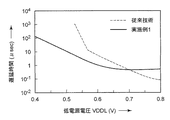
図17は、低電源電圧VDDLの電圧値に対する図3Bのレベルコンバータ回路1及び従来技術に係るレベルコンバータ回路100の遅延時間を示すグラフである。図3Bのレベルコンバータ回路1の遅延時間を図2に示した従来技術に係るレベルコンバータ回路100の遅延時間と比較する。従来技術に係るレベルコンバータ回路100は、低電源電圧VDDLが0.7V以上のときに、レベルコンバータ回路1よりも高速に動作する。しかし、低電源電圧VDDLが低下するにつれ、レベルコンバータ回路100の動作遅延は指数関数的に増大し、低電源電圧VDDLが約0.52V以下になると、レベルコンバータ回路100は、動作することができない。これは、従来技術に係るレベルコンバータ回路100では、出力信号OUTの電圧を低下させるために端子T102を放電する電流は、低電源電圧VDDLの電圧に依存するためである。すなわち、低電源電圧VDDLが低電圧になるほどnMOSトランジスタMN102を流れる電流が減少し、遅延時間が指数関数的に増大する。そして、低電源電圧VDDLが約0.52V以下になるとnMOSトランジスタMN102を流れる電流量よりpMOSトランジスタMP102を流れる電流量の方が多くなり、出力信号OUTの論理は反転することなく、レベルコンバータ回路100は動作を停止する。   FIG. 17 is a graph showing the delay time of the level converter circuit 1 of FIG. 3B and the level converter circuit 100 according to the prior art with respect to the voltage value of the low power supply voltage VDDL. The delay time of the level converter circuit 1 in FIG. 3B is compared with the delay time of the level converter circuit 100 according to the prior art shown in FIG. The level converter circuit 100 according to the prior art operates faster than the level converter circuit 1 when the low power supply voltage VDDL is 0.7 V or higher. However, as the low power supply voltage VDDL decreases, the operation delay of the level converter circuit 100 increases exponentially, and when the low power supply voltage VDDL is about 0.52 V or less, the level converter circuit 100 cannot operate. . This is because in the level converter circuit 100 according to the prior art, the current that discharges the terminal T102 to reduce the voltage of the output signal OUT depends on the voltage of the low power supply voltage VDDL. That is, as the low power supply voltage VDDL becomes lower, the current flowing through the nMOS transistor MN102 decreases and the delay time increases exponentially. When the low power supply voltage VDDL is about 0.52 V or less, the amount of current flowing through the pMOS transistor MP102 becomes larger than the amount of current flowing through the nMOS transistor MN102, and the level converter circuit 100 does not invert the logic of the output signal OUT. Stops working.

一方、レベルコンバータ回路1では、電流生成回路10によって生成される電流IA1の電流量で遅延時間が決定される。低電源電圧VDDLが0.65V付近よりも低い領域では、電流生成回路10のnMOSトランジスタMN11,MN12が、サブスレッショルド領域で動作する。このため、図14に示すように、電流IA1の電流量が低電源電圧VDDLに対して指数関数的に変化する。これにより、低電源電圧VDDLの上昇に従って、遅延時間が指数関数的に減少する。また、低電源電圧VDDLが約0.65Vより高い領域では、遅延時間はほぼ一定となる。これは、低電源電圧VDDLが0.65V以上になると電流生成回路10によって生成される電流IA1は増加するものの、図15に示すようにカレントミラー回路のローパスフィルタの効果によって生成される電流IA1の供給能力が減少する。その結果、差動増幅回路30に流れる電流IA2及びソース接地増幅回路40に流れる電流IA3は増加せず、遅延時間はほぼ一定となる。このことは、図17の遅延時間の逆数である周波数がMHzオーダーであることからも図15の結果と一致する。レベルコンバータ回路1は、電流生成回路10によって生成される電流IA1に対応する電流を用いて、端子T2に対する充電及び放電の両方を実行するため、従来技術に係るレベルコンバータ回路100が有する問題は発生せず、低電源電圧VDDLと高電源電圧VDDHとの間の電源電圧の差が大きくなるような低い低電源電圧VDDLにおいても安定に動作する。 On the other hand, in the level converter circuit 1, the delay time is determined by the current amount of the current IA1 generated by the current generation circuit 10. In a region where the low power supply voltage VDDL is lower than around 0.65 V, the nMOS transistors MN11 and MN12 of the current generation circuit 10 operate in the subthreshold region. For this reason, as shown in FIG. 14, the amount of current I A1 changes exponentially with respect to the low power supply voltage VDDL. As a result, the delay time decreases exponentially as the low power supply voltage VDDL increases. In the region where the low power supply voltage VDDL is higher than about 0.65 V, the delay time is substantially constant. This is because the current I A1 generated by the current generation circuit 10 increases when the low power supply voltage VDDL becomes 0.65 V or more, but the current I generated by the effect of the low-pass filter of the current mirror circuit as shown in FIG. A1 supply capacity decreases. As a result, the current I A2 flowing through the differential amplifier circuit 30 and the current I A3 flowing through the common source amplifier circuit 40 do not increase, and the delay time becomes substantially constant. This agrees with the result of FIG. 15 because the frequency which is the reciprocal of the delay time of FIG. 17 is in the order of MHz. Since the level converter circuit 1 uses the current corresponding to the current I A1 generated by the current generation circuit 10 to perform both charging and discharging of the terminal T2, the problem of the level converter circuit 100 according to the related art is It does not occur and operates stably even at a low power supply voltage VDDL where the difference in power supply voltage between the low power supply voltage VDDL and the high power supply voltage VDDH is large.

図18は、低電源電圧VDDLの電圧値に対する図3Bのレベルコンバータ回路1及び従来技術に係るレベルコンバータ回路100の消費電力を示すグラフである。ここでは、入力信号INの周波数は1kHzである。また、図3Bのレベルコンバータ回路1の消費電力を図2に示した従来技術に係るレベルコンバータ回路100の消費電力と比較する。図18より明らかなとおり、レベルコンバータ回路1は、従来技術に係るレベルコンバータ回路100と比較して、低消費電力で動作可能である。従来技術に係るレベルコンバータ回路100は、高電圧源から多量の貫通電流が流れるため消費電力が高くなる。   FIG. 18 is a graph showing the power consumption of the level converter circuit 1 of FIG. 3B and the level converter circuit 100 according to the prior art with respect to the voltage value of the low power supply voltage VDDL. Here, the frequency of the input signal IN is 1 kHz. 3B is compared with the power consumption of the level converter circuit 100 according to the prior art shown in FIG. As is clear from FIG. 18, the level converter circuit 1 can operate with lower power consumption than the level converter circuit 100 according to the prior art. The level converter circuit 100 according to the related art has high power consumption because a large amount of through current flows from a high voltage source.

また、図18において、従来技術に係るレベルコンバータ回路100の消費電力が、低電源電圧VDDLの上昇とともに指数関数的に減少していることが確認できる。これは、低電源電圧VDDLで動作するロジック回路の信号波形が原因である。低電源電圧VDDLで動作するロジック回路においては、トランジスタの電流駆動能力が極めて低くなり、信号が緩やかに変化する。そのため、0.55V程度の低電源電圧VDDLでは、信号の遷移時間が長くなり、高電圧源から多量の貫通電流が流れる。一方で、低電源電圧VDDLの上昇とともに、信号は急峻に変化するため、高電圧源からの貫通電流が減少する。   Further, in FIG. 18, it can be confirmed that the power consumption of the level converter circuit 100 according to the prior art decreases exponentially as the low power supply voltage VDDL increases. This is due to the signal waveform of the logic circuit operating at the low power supply voltage VDDL. In a logic circuit that operates with the low power supply voltage VDDL, the current drive capability of the transistor becomes extremely low, and the signal changes slowly. Therefore, at a low power supply voltage VDDL of about 0.55 V, the signal transition time becomes long, and a large amount of through current flows from the high voltage source. On the other hand, since the signal changes sharply as the low power supply voltage VDDL increases, the through current from the high voltage source decreases.

一方、レベルコンバータ回路1の消費電力は、低電源電圧VDDLが変化しても、ほぼ変化しない。これは、低電源電圧VDDLの上昇による次の2つの要因に起因する。
(1)電流生成回路10によって生成される電流IA1の増加。
(2)低電源電圧VDDLによって駆動されるロジック回路の信号の遅延改善。
図14に示すとおり、電流生成回路10によって生成される電流IA1が、低電源電圧VDDLの上昇に従って指数関数的に増加する。一方で、低電源電圧VDDLの上昇に従って低電源電圧VDDLで動作するロジック回路の遅延時間は指数関数的に減少する。これら2つの要因により、瞬間的に流れる電流IA1は指数関数的に増加するが、電流IA1が流れる時間は指数関数的に短くなるので、最終的に流れる電流IA1の全体量はほぼ変化しない。したがって、レベルコンバータ回路1の消費電力は、低電源電圧VDDLに対する依存性が小さい。
On the other hand, the power consumption of the level converter circuit 1 hardly changes even when the low power supply voltage VDDL changes. This is due to the following two factors due to the rise of the low power supply voltage VDDL.
(1) An increase in the current I A1 generated by the current generation circuit 10.
(2) Improvement of signal delay of logic circuit driven by low power supply voltage VDDL.
As shown in FIG. 14, the current I A1 generated by the current generation circuit 10 increases exponentially as the low power supply voltage VDDL increases. On the other hand, the delay time of the logic circuit operating at the low power supply voltage VDDL decreases exponentially as the low power supply voltage VDDL increases. Due to these two factors, the instantaneously flowing current I A1 increases exponentially, but the time during which the current I A1 flows exponentially decreases, so that the total amount of the finally flowing current I A1 changes substantially. do not do. Therefore, the power consumption of the level converter circuit 1 is less dependent on the low power supply voltage VDDL.

表1は、図3Bのレベルコンバータ回路1及び従来技術に係るレベルコンバータ回路100のプロセスバラツキ及び温度変化に対する耐性を示す。表1では、低電源電圧VDDLは0.6Vである。また、表1中のFF,FS,TT,SF,SSは、nMOSトランジスタ及びpMOSトランジスタのコーナーモデルを表し、Pは当該レベルコンバータ回路が正常に動作するパス状態を表し、Fは当該レベルコンバータ回路が正常に動作しないフェイル状態を表す。   Table 1 shows the process resistance of the level converter circuit 1 of FIG. 3B and the level converter circuit 100 according to the prior art and resistance to temperature changes. In Table 1, the low power supply voltage VDDL is 0.6V. In Table 1, FF, FS, TT, SF, and SS represent corner models of nMOS transistors and pMOS transistors, P represents a path state in which the level converter circuit operates normally, and F represents the level converter circuit. Indicates a failure state in which does not operate normally.

Figure 0005215356
Figure 0005215356

従来技術に係るレベルコンバータ回路100は、プロセスバラツキ及び温度変化によってnMOSトランジスタのしきい値電圧が高くなると、正常に動作しなくなる。これは、遅延時間の低電源電圧VDDLに対する依存性の結果と同様に、nMOSトランジスタMN102を流れる電流がpMOSトランジスタMP102を流れるリーク電流よりも小さくなることで、端子T102が放電されないためである。一方、レベルコンバータ回路1は、プロセスバラツキ及び温度変化に対して安定に動作する。   The level converter circuit 100 according to the prior art does not operate normally when the threshold voltage of the nMOS transistor increases due to process variations and temperature changes. This is because the terminal T102 is not discharged because the current flowing through the nMOS transistor MN102 is smaller than the leak current flowing through the pMOS transistor MP102, as in the result of the dependency of the delay time on the low power supply voltage VDDL. On the other hand, the level converter circuit 1 operates stably with respect to process variations and temperature changes.

本発明者らは、レベルコンバータ回路1の有効性を確認するために、チップを試作した。試作チップの信号波形及び消費電力の測定結果を以下に示す。使用したプロセスは0.35μm 2P−4M CMOSプロセスである。図19に試作チップの写真を示す。回路面積は、43μm×43μmと小面積である。   In order to confirm the effectiveness of the level converter circuit 1, the inventors made a prototype chip. The measurement results of the signal waveform and power consumption of the prototype chip are shown below. The process used is a 0.35 μm 2P-4M CMOS process. FIG. 19 shows a photograph of the prototype chip. The circuit area is a small area of 43 μm × 43 μm.

図20は、図19の試作チップの動作を測定するための測定環境を示すブロック図である。図20に示すように、パッケージされた試作チップ402をボード上に実装して測定を行った。ファンクションジェネレータ401を用いて低振幅の入力信号INを生成し、レベルコンバータ回路(試作チップ402)に入力する。ファンクションジェネレータ401からの入力信号IN及びレベルコンバータ回路からの出力信号OUTをオシロスコープ403に入力して評価した。また、高電源電圧VDDHは3Vである。   FIG. 20 is a block diagram showing a measurement environment for measuring the operation of the prototype chip of FIG. As shown in FIG. 20, the packaged prototype chip 402 was mounted on a board and measured. A low-amplitude input signal IN is generated using the function generator 401 and input to the level converter circuit (prototype chip 402). The input signal IN from the function generator 401 and the output signal OUT from the level converter circuit were input to the oscilloscope 403 for evaluation. The high power supply voltage VDDH is 3V.

図21(a)は、図20の測定環境において、試作チップ402への入力信号INの波形を示すグラフであり、図21(b)は、図20の測定環境において、試作チップからの出力信号OUTの波形を示すグラフである。図21は、低電源電圧VDDLが0.4V、入力信号INの周波数が10kHzであるときの入力信号INの波形及び出力信号OUTの波形を示す。0.4Vの振幅を有する低振幅の入力信号INが、レベルコンバータ回路1によって3Vの振幅を有する大振幅の出力信号OUTにレベル変換されている様子が確認できる。   FIG. 21A is a graph showing the waveform of the input signal IN to the prototype chip 402 in the measurement environment of FIG. 20, and FIG. 21B is an output signal from the prototype chip in the measurement environment of FIG. It is a graph which shows the waveform of OUT. FIG. 21 shows the waveform of the input signal IN and the waveform of the output signal OUT when the low power supply voltage VDDL is 0.4 V and the frequency of the input signal IN is 10 kHz. It can be confirmed that a low-amplitude input signal IN having an amplitude of 0.4 V is level-converted by the level converter circuit 1 to a large-amplitude output signal OUT having an amplitude of 3 V.

また、図21の結果から、入力信号INが変化してから、出力信号OUTが変化するまでの立ち上がり時間と立ち下がり時間とが異なることがわかる。その結果、出力信号OUTのデューティ比が50%以下となった。これは、レベルコンバータ回路1の特性に起因する。図3Bに示したレベルコンバータ回路1の端子T2の充放電は、pMOSトランジスタMP41及びnMOSトランジスタMN41に流れる電流によって行われる。このとき、出力信号OUTの立ち上がり時間は、pMOSトランジスタMP41を流れる電流、すなわち、カレントミラー回路を介して供給される電流生成回路10によって生成される電流IA1に対応する電流によって決まる。一方、nMOSトランジスタMN41を流れる電流は、nMOSトランジスタMN41のゲートに印加される電圧によって決まる。nMOSトランジスタMN41のゲートの容量を充放電するための時間も、カレントミラー回路を介して供給される電流生成回路10によって生成される電流IA1に対応する電流によって決まるが、差動増幅回路30の回路構成の特性から、pMOSトランジスタMP41によって端子T2が充電される時間と、nMOSトランジスタMN41によって端子T2が放電される時間とは異なる。そのため、出力信号OUTの立ち上がり時間と立ち下がり時間とが異なる結果となる。今後は、立ち上がり時間と立ち下がり時間とが等しくなるような回路を構成するなど、デューティ比を50%に近づける必要がある。 Further, it can be seen from the result of FIG. 21 that the rise time and the fall time from when the input signal IN changes to when the output signal OUT changes are different. As a result, the duty ratio of the output signal OUT became 50% or less. This is due to the characteristics of the level converter circuit 1. Charging / discharging of the terminal T2 of the level converter circuit 1 shown in FIG. 3B is performed by a current flowing through the pMOS transistor MP41 and the nMOS transistor MN41. At this time, the rise time of the output signal OUT is determined by the current flowing through the pMOS transistor MP41, that is, the current corresponding to the current I A1 generated by the current generation circuit 10 supplied via the current mirror circuit. On the other hand, the current flowing through the nMOS transistor MN41 is determined by the voltage applied to the gate of the nMOS transistor MN41. The time for charging and discharging the capacitance of the gate of the nMOS transistor MN41 is also determined by the current corresponding to the current I A1 generated by the current generation circuit 10 supplied through the current mirror circuit. Due to the characteristics of the circuit configuration, the time during which the terminal T2 is charged by the pMOS transistor MP41 is different from the time during which the terminal T2 is discharged by the nMOS transistor MN41. For this reason, the rise time and fall time of the output signal OUT are different. In the future, it is necessary to make the duty ratio close to 50%, for example, by configuring a circuit in which the rise time and the fall time are equal.

図22は、図19の試作チップのシュム(Shmoo)プロットを示す図である。低電源電圧VDDLに対して、レベルコンバータ回路1が動作可能な周波数帯をプロットしている。低電源電圧VDDLが0.4Vから0.64V付近であるとき、動作可能な最大周波数が指数関数的に増加している。これは、低電源電圧VDDLの上昇に従って電流生成回路10によって生成される電流IA1が指数関数的に増加するためである。低電源電圧VDDLが0.64Vを超えると動作可能な周波数は2MHz付近からほぼ一定となる。これは、図17に示したシミュレーション結果と同様に、カレントミラー回路のローパスフィルタの効果により、電流生成回路10によって生成された電流IA1の高周波成分が差動増幅回路30及びソース接地増幅回路40に供給されず、差動増幅回路30及びソース接地増幅回路40に流れる電流が制限されるためである。 FIG. 22 is a diagram showing a Shmoo plot of the prototype chip of FIG. The frequency band in which the level converter circuit 1 can operate with respect to the low power supply voltage VDDL is plotted. When the low power supply voltage VDDL is in the vicinity of 0.4V to 0.64V, the maximum operable frequency increases exponentially. This is because the current I A1 generated by the current generation circuit 10 increases exponentially as the low power supply voltage VDDL increases. When the low power supply voltage VDDL exceeds 0.64 V, the operable frequency becomes substantially constant from around 2 MHz. As in the simulation result shown in FIG. 17, the high-frequency component of the current I A1 generated by the current generation circuit 10 is converted into the differential amplifier circuit 30 and the source grounded amplifier circuit 40 by the effect of the low-pass filter of the current mirror circuit. This is because the current flowing through the differential amplifier circuit 30 and the common source amplifier circuit 40 is limited.

図23は、低電源電圧VDDLの電圧値に対する図19の試作チップの消費電力を示すグラフである。ここでは、入力信号INの周波数は10kHzである。試作チップの消費電力は、低電源電圧VDDLへの依存性が小さく、低電源電圧VDDLの上昇とともに減少している。これは、図18のシミュレーション結果と一致する。   FIG. 23 is a graph showing the power consumption of the prototype chip of FIG. 19 with respect to the voltage value of the low power supply voltage VDDL. Here, the frequency of the input signal IN is 10 kHz. The power consumption of the prototype chip is less dependent on the low power supply voltage VDDL and decreases as the low power supply voltage VDDL increases. This agrees with the simulation result of FIG.

レベルコンバータ回路1は、クロスカップル型レベルコンバータ回路100よりも低消費電力で動作し、かつ低電源電圧VDDLが低電圧であっても安定に動作することから、低電圧動作LSIに有用である。   Since the level converter circuit 1 operates with lower power consumption than the cross-coupled level converter circuit 100 and operates stably even when the low power supply voltage VDDL is a low voltage, it is useful for a low-voltage operation LSI.

第1の実施形態では、回路ブロック間の電源電圧の差電圧が大きい場合でも安定に動作可能なレベルコンバータ回路1を提案した。レベルコンバータ回路1は、2段増幅回路を基本とした回路を構成することで、従来技術に係るレベルコンバータ回路100の問題点である充放電部分の電源電圧差依存性を緩和する。さらに、レベルコンバータ回路1は入力信号INが変化するときのみ電力を消費することから低消費電力で動作することができる。0.35μm標準CMOSプロセスを用いてチップを試作し、測定により動作を確認した。レベルコンバータ回路1を用いることで、0.4V振幅の低電圧信号を3V振幅の高電圧信号に変換することができる。レベルコンバータ回路1は、低消費電力、低電圧動作LSIに有用である。   In the first embodiment, the level converter circuit 1 has been proposed that can operate stably even when the voltage difference between the power supply voltages between the circuit blocks is large. The level converter circuit 1 constitutes a circuit based on a two-stage amplifier circuit, thereby reducing the dependency of the charge / discharge portion on the power supply voltage difference, which is a problem of the level converter circuit 100 according to the prior art. Furthermore, since the level converter circuit 1 consumes power only when the input signal IN changes, it can operate with low power consumption. A chip was prototyped using a 0.35 μm standard CMOS process, and the operation was confirmed by measurement. By using the level converter circuit 1, it is possible to convert a low voltage signal having a 0.4V amplitude into a high voltage signal having a 3V amplitude. The level converter circuit 1 is useful for low power consumption and low voltage operation LSIs.

第2の実施形態に係るレベルコンバータ回路1Aについてのシミュレーション評価(実施例2)について以下説明する。本発明者らは、レベルコンバータ回路1Aの動作を確認するためのシミュレーション評価を行った。使用したCMOSプロセスは、0.35μmCMOSプロセスである。   A simulation evaluation (Example 2) for the level converter circuit 1A according to the second embodiment will be described below. The present inventors performed a simulation evaluation for confirming the operation of the level converter circuit 1A. The CMOS process used is a 0.35 μm CMOS process.

本発明者らは、レベルコンバータ回路1Aのシミュレーション評価を行った。ここで、低電源電圧VDDLは0.4Vであり、高電源電圧VDDHは3.0Vである。シミュレーションの結果を図24〜図27に示す。図24は、図11Bのレベルコンバータ回路1Aへの入力信号IN,INBの波形及び図11Bのレベルコンバータ回路1Aからの出力信号OUTの波形を示すグラフである。図25は、図12の変化時電流生成回路11によって生成される電流Iの波形を示すグラフである。図26は、図12の立ち下がり電流生成回路13によって生成される電流Iの波形を示すグラフである。図27は、図12の立ち上がり電流生成回路12によって生成される電流Iの波形を示すグラフである。 The present inventors performed a simulation evaluation of the level converter circuit 1A. Here, the low power supply voltage VDDL is 0.4V, and the high power supply voltage VDDH is 3.0V. The simulation results are shown in FIGS. FIG. 24 is a graph showing the waveforms of the input signals IN and INB to the level converter circuit 1A of FIG. 11B and the waveform of the output signal OUT from the level converter circuit 1A of FIG. 11B. Figure 25 is a graph showing the waveform of the current I C that is generated by the change time of the current generation circuit 11 in FIG. 12. Figure 26 is a graph showing the waveform of the current I F generated by the falling current generation circuit 13 in FIG. 12. Figure 27 is a graph showing the waveform of the current I R generated by the rising current generation circuit 12 in FIG. 12.

図24に示すように、入力信号INの論理に一致して出力信号OUTがレベル変換されて出力されている。また、入力信号INの立ち上がりと入力信号INBの立ち下がりとにおいては、波形が重なっているが、入力信号INの立ち下がりと入力信号INBの立ち上がりとにおいては、波形が重なっていない。これは、入力信号INの立ち下がりでは電流Iが正しく生成されないことを意味する。 As shown in FIG. 24, the output signal OUT is level-converted and output in accordance with the logic of the input signal IN. Further, the waveforms overlap at the rising edge of the input signal IN and the falling edge of the input signal INB, but the waveforms do not overlap at the falling edge of the input signal IN and the rising edge of the input signal INB. This is because the fall of the input signal IN means that the current I C is not properly generated.

図25に示すように、入力信号INの立ち上がり時に、変化時電流生成回路11は、正常に電流Iを生成している(1ナノアンペアオーダーのピーク電流である。)。一方、入力信号INの立ち下がり時には、変化時電流生成回路11は、電流Iを生成しているように見える(2ナノアンペアオーダーのピーク電流である。)。しかし、上述のように、入力信号INの立ち下がりでは、入力信号INと入力信号INBとは重ならないため、変化時電流生成回路11が正常動作しているとはいえない。この電流Iは、出力信号OUTのキックバック現象によって生成された電流であり、変化時電流生成回路11によって生成された電流ではない。 As shown in FIG. 25, when the rise of the input signal IN, the change time of the current generation circuit 11, normally current is generating the I C (a first peak current of nA order.). On the other hand, at the falling edge of the input signal IN is changed during current generation circuit 11, it appears to generate a current I C (a 2 nano-amperes peak current.). However, as described above, since the input signal IN and the input signal INB do not overlap at the falling edge of the input signal IN, it cannot be said that the change-time current generation circuit 11 is operating normally. The current I C is the current generated by the kick back phenomenon of the output signal OUT, not the current generated by the change time of the current generation circuit 11.

しかしながら、レベルコンバータ回路1Aは、所望の動作(すなわち、ローレベルの出力信号OUTを出力する。)を行っている。これは、レベルコンバータ回路1Aのレベル変換動作が、差動増幅回路30及びソース接地増幅回路40における出力信号OUTの立ち上がり時間の遅延時間並びに立ち下がり時間の遅延時間、及び電流生成回路10Aの遅延時間に依存するためである。レベルコンバータ回路1Aの差動増幅回路30及びソース接地増幅回路40では、出力信号OUTの立ち上がり遅延時間はpMOSトランジスタMP41の充電電流IA3で決定され、出力信号OUTの立ち下がり時間はnMOSトランジスタMN41の放電電流IA4で決定される。充電電流IA3は電流生成回路10Aによって生成される電流IA1に依存する一方で、放電電流IA4は電流生成回路10Aによって生成される電流に依存しないことが考えられる。 However, the level converter circuit 1A performs a desired operation (that is, outputs a low level output signal OUT). This is because the level conversion operation of the level converter circuit 1A is the delay time of the rise time and the fall time of the output signal OUT in the differential amplifier circuit 30 and the common source amplifier circuit 40, and the delay time of the current generation circuit 10A. Because it depends on. In the differential amplifier circuit 30 and the source-grounded amplifier circuit 40 of the level converter circuit 1A, the rise delay time of the output signal OUT is determined by the charging current I A3 of the pMOS transistor MP41, the fall time of the output signal OUT of the nMOS transistor MN41 It is determined by the discharge current I A4 . It is conceivable that the charging current I A3 depends on the current I A1 generated by the current generation circuit 10A, while the discharging current I A4 does not depend on the current generated by the current generation circuit 10A.

これを図11Bに示す差動増幅回路30及びソース接地増幅回路40の回路図で考える。充電電流IA3は、pMOSトランジスタMP21,MP41で構成されるカレントミラー回路を介して供給される電流生成回路10Aによって生成された電流IA1に対応する電流である。一方、放電電流IA4は、ソース接地増幅回路40のnMOSトランジスタMN41のゲート電圧、すなわち差動増幅回路30のノードN31の電圧に依存する。ノードN31の電圧は、入力信号INがローレベルとなると、ローレベルから第1のハイレベルの近傍電圧に変化する。ノードN31の電圧は、nMOSトランジスタMN41のゲートに印加されるため、出力信号OUTは立ち下がってローレベルとなる。ノードN31の電圧は、電流生成回路10Aによって生成される電流IA1に依存せず、第1のハイレベルの近傍電圧となって出力信号OUTを立ち下げる。すなわち、差動増幅回路30及びソース接地増幅回路40では、出力信号OUTの立ち上がり遅延時間が長く、立ち下がり遅延時間が短い。立ち上がり遅延時間が長いため、入力信号INの立ち上がりにおいて論理不一致が生じ、電流生成回路10Aの立ち上がり電流生成回路12が論理不一致を検出し、電流Iを生成して出力信号OUTの立ち上がりを加速させる。一方、レベルコンバータ回路1Aの差動増幅回路30及びソース接地増幅回路40は、出力信号OUTの立ち下がり時には素早く反応するため、立ち下がり電流生成回路13は動作せずともレベルコンバータ回路1Aはローレベルの出力信号OUTを出力することができる。 This is considered in the circuit diagram of the differential amplifier circuit 30 and the common source amplifier circuit 40 shown in FIG. 11B. The charging current I A3 is a current corresponding to the current I A1 generated by the current generating circuit 10A supplied via the current mirror circuit configured by the pMOS transistors MP21 and MP41. On the other hand, the discharge current I A4 depends on the gate voltage of the nMOS transistor MN41 of the common source amplifier circuit 40, that is, the voltage of the node N31 of the differential amplifier circuit 30. The voltage of the node N31 changes from the low level to the first high level neighborhood voltage when the input signal IN becomes the low level. Since the voltage of the node N31 is applied to the gate of the nMOS transistor MN41, the output signal OUT falls and becomes a low level. The voltage at the node N31 does not depend on the current I A1 generated by the current generation circuit 10A, and becomes a first high-level neighborhood voltage to cause the output signal OUT to fall. That is, in the differential amplifier circuit 30 and the common source amplifier circuit 40, the rise delay time of the output signal OUT is long and the fall delay time is short. Since the rise delay time is long, the logic mismatch occurs at the rise of the input signal IN, the rise current generator circuit 12 of the current generation circuit 10A detects a logical inconsistency, to accelerate the rise of the output signal OUT to generate a current I R . On the other hand, the differential amplifier circuit 30 and the grounded source amplifier circuit 40 of the level converter circuit 1A react quickly when the output signal OUT falls, so that the level converter circuit 1A does not operate even if the falling current generator circuit 13 does not operate. Output signal OUT can be output.

図26に示すように、電流Iが生成されていないことが確認できる。これは、上述のように出力信号OUTの立ち下がり遅延時間が短いので、電流生成回路10Aが動作を開始する前に、出力信号OUTがローレベルに立ち下がるからである。一方、出力信号OUTの立ち上がりにおいて、図25に示すように電流Iが生成されているが、出力信号OUTを立ち上げるのに十分な電流量とは言えず、立ち上がり電流生成回路12が論理不一致を検出し、電流Iを生成する。図27に示すように、出力信号OUTの立ち上がりにおいて、電流Iが生成されていることが確認できる。 As shown in FIG. 26, it can be confirmed that the current IF is not generated. This is because the fall delay time of the output signal OUT is short as described above, so that the output signal OUT falls to the low level before the current generation circuit 10A starts its operation. On the other hand, the rising of the output signal OUT, although current I C is generated as shown in FIG. 25, not sufficient amount of current to start up the output signal OUT, rising current generation circuit 12 is a logical inconsistency detects, it generates a current I R. As shown in FIG. 27, at the rise of the output signal OUT, it can be confirmed that the current I R is produced.

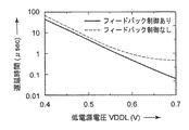
図28は、低電源電圧VDDLの電圧値に対する図11Bのレベルコンバータ回路1A及び図3Bのレベルコンバータ回路1の遅延時間を示すグラフである。図28において、フィードバック制御を有するレベルコンバータ回路1Aの遅延時間は実線で示され、フィードバック制御を有しないレベルコンバータ回路1の遅延時間は破線で示される。図28に示すように、レベルコンバータ回路1Aの遅延時間は、低電源電圧VDDLの上昇とともに減少することが確認できる。また、レベルコンバータ回路1Aは、レベルコンバータ回路1と比較して、高速に動作することが確認できる。低電源電圧VDDLが約0.55V以下の低電圧では、レベルコンバータ回路1Aはレベルコンバータ回路1よりも数倍程度高速に動作し、低電源電圧VDDLが高くなるにつれて、その差は大きくなることが確認できる。立ち上がり電流生成回路12によって生成される電流I及び立ち下がり電流生成回路13によって生成される電流Iが差動増幅回路30及びソース接地増幅回路40の動作電流に加算されることが、レベルコンバータ回路1Aの高速動作に繋がっているといえる。 FIG. 28 is a graph showing the delay time of the level converter circuit 1A of FIG. 11B and the level converter circuit 1 of FIG. 3B with respect to the voltage value of the low power supply voltage VDDL. In FIG. 28, the delay time of the level converter circuit 1A having feedback control is indicated by a solid line, and the delay time of the level converter circuit 1 not having feedback control is indicated by a broken line. As shown in FIG. 28, it can be confirmed that the delay time of the level converter circuit 1A decreases as the low power supply voltage VDDL increases. Further, it can be confirmed that the level converter circuit 1A operates at a higher speed than the level converter circuit 1. When the low power supply voltage VDDL is about 0.55 V or less, the level converter circuit 1A operates several times faster than the level converter circuit 1, and the difference increases as the low power supply voltage VDDL increases. I can confirm. That current I F generated by the current I R and the falling current generator circuit 13 is generated by the rise current generator circuit 12 is added to the operating current of the differential amplifier circuit 30 and the source-grounded amplifier circuit 40, the level converter It can be said that this leads to high-speed operation of the circuit 1A.

図29は、低電源電圧VDDLの電圧値に対する図11Bのレベルコンバータ回路1A及び図3Bのレベルコンバータ回路1の消費電力を示すグラフである。図29において、フィードバック制御を有するレベルコンバータ回路1Aの消費電力は実線で示され、フィードバック制御を有しないレベルコンバータ回路1の消費電力は破線で示される。レベルコンバータ回路1Aは、レベルコンバータ回路1よりも消費電力が多い。これは、立ち上がり電流生成回路12によって生成される電流I及び立ち下がり電流生成回路13によって生成される電流Iが、差動増幅回路30及びソース接地増幅回路40の動作電流に加算されるためである。しかし、増加する消費電力は、ナノワットオーダーの微小電力に抑えることができている。 FIG. 29 is a graph showing power consumption of the level converter circuit 1A of FIG. 11B and the level converter circuit 1 of FIG. 3B with respect to the voltage value of the low power supply voltage VDDL. In FIG. 29, the power consumption of the level converter circuit 1A having feedback control is indicated by a solid line, and the power consumption of the level converter circuit 1 not having feedback control is indicated by a broken line. The level converter circuit 1A consumes more power than the level converter circuit 1. This is because the current I F generated by the current I R and the falling current generator circuit 13 is generated by the rise current generator circuit 12 is added to the operating current of the differential amplifier circuit 30 and the source-grounded amplifier circuit 40 It is. However, the increased power consumption can be suppressed to a minute power of nanowatt order.

本発明者らは、電流生成回路10Aの特性評価を行うためのシミュレーション評価を行った。ここでは、図12に示す電流生成回路10Aにおいて、以下の2つのシミュレーションを実行した。
シミュレーション1:入力信号INを第1のハイレベルに固定し、入力信号INBをローレベルに固定し、出力信号OUTを0Vから3Vまで変化させて、立ち上がり電流生成回路12によって生成される電流I及び立ち下がり電流生成回路13によって生成される電流Iを測定する。
シミュレーション2:入力信号INをローレベルに固定し、入力信号INBを第1のハイレベルに固定し、出力信号OUTを0Vから3Vまで変化させて、立ち上がり電流生成回路12によって生成される電流I及び立ち下がり電流生成回路13によって生成される電流Iを測定する。
The present inventors performed a simulation evaluation for evaluating the characteristics of the current generation circuit 10A. Here, the following two simulations were executed in the current generation circuit 10A shown in FIG.
Simulation 1: The input signal IN is fixed to the first high level, the input signal INB is fixed to the low level, and the output signal OUT is changed from 0 V to 3 V, and the current I R generated by the rising current generation circuit 12 is changed. and measuring the current I F generated by the fall current generator circuit 13.
Simulation 2: The input signal IN is fixed to the low level, the input signal INB is fixed to the first high level, the output signal OUT is changed from 0V to 3V, and the current I R generated by the rising current generation circuit 12 is changed. and measuring the current I F generated by the fall current generator circuit 13.

まず、シミュレーション1の結果について説明する。図30Aは、図12の電流生成回路10Aにおいて、入力信号INを第1のハイレベルに固定し、入力信号INBをローレベルに固定し、出力信号OUTを0Vから3Vに変化させた場合に生成される電流Iを示すグラフである。また、図30Bは、図12の電流生成回路10Aにおいて、入力信号INを第1のハイレベルに固定し、入力信号INBをローレベルに固定し、出力信号OUTを0Vから3Vに変化させた場合に生成される電流Iを示すグラフである。 First, the result of the simulation 1 will be described. 30A is generated when the input signal IN is fixed at the first high level, the input signal INB is fixed at the low level, and the output signal OUT is changed from 0V to 3V in the current generation circuit 10A of FIG. is a graph showing the current I F to be. 30B shows a case where the input signal IN is fixed to the first high level, the input signal INB is fixed to the low level, and the output signal OUT is changed from 0V to 3V in the current generation circuit 10A of FIG. is a graph showing the current I R that is generated.

入力信号INが第1のハイレベルであり、入力信号INBがローレベルであるため、出力信号OUTは第2のハイレベルであることが理想である。図30Bに示すように、出力信号OUTが約2.4V以下の低い電圧である場合、電流Iが生成されることが確認できる。この電流Iは、出力信号OUTを上昇させるようにカレントミラー回路を介して差動増幅回路30及びソース接地増幅回路40に供給される。一方、出力信号OUTが高い電圧、すなわち第2のハイレベルに近い場合、電流Iは生成されないことが確認できる。また、このとき、入力信号INBはローレベルであり、出力信号OUTを立ち下げる必要はないため、図30Aに示すように電流Iは生成されない。電流Iの電流量(シミュレーション1では約17nAである。)は、低電源電圧VDDLの値(シミュレーション1では0.4Vである。)に依存する。低電源電圧VDDLが上昇すると、電流Iは増大する。 Since the input signal IN is at the first high level and the input signal INB is at the low level, the output signal OUT is ideally at the second high level. As shown in FIG. 30B, when the output signal OUT is approximately 2.4V less low voltage, it can be confirmed that the current I R is produced. The current I R is supplied to the differential amplifier circuit 30 and the source-grounded amplifier circuit 40 via the current mirror circuit to raise the output signal OUT. On the other hand, the output signal OUT is high voltage, that is, when close to the second high level, the current I R can confirm not be generated. At this time, the input signal INB is at a low level, since it is not necessary to fall the output signal OUT, a current I F as shown in FIG. 30A is not generated. The current amount of the current I R (a the simulation 1 to about 17nA.) Depends on the value of the low power supply voltage VDDL (the simulation 1 is 0.4V.). When the low power supply voltage VDDL rises, the current I R will increase.

次に、シミュレーション2の結果について説明する。図31Aは、図12の電流生成回路10Aにおいて、入力信号INをローレベルに固定し、入力信号INBを第1のハイレベルに固定し、出力信号OUTを0Vから3Vに変化させた場合に生成される電流Iを示すグラフである。また、図31Bは、図12の電流生成回路10Aにおいて、入力信号INをローレベルに固定し、入力信号INBを第1のハイレベルに固定し、出力信号OUTを0Vから3Vに変化させた場合に生成される電流Iを示すグラフである。 Next, the result of the simulation 2 will be described. FIG. 31A is generated when the input signal IN is fixed to a low level, the input signal INB is fixed to a first high level, and the output signal OUT is changed from 0V to 3V in the current generation circuit 10A of FIG. is a graph showing the current I F to be. FIG. 31B shows a case where the input signal IN is fixed at a low level, the input signal INB is fixed at a first high level, and the output signal OUT is changed from 0V to 3V in the current generation circuit 10A of FIG. is a graph showing the current I R that is generated.

入力信号INがローレベルであり、入力信号INBが第1のハイレベルであるため、出力信号OUTはローレベルであることが理想である。図31Aに示すように、出力信号OUTが約0.3V以上の高い電圧である場合、電流Iが生成されることが確認できる。この電流Iは、出力信号OUTを低下させるようにカレントミラー回路を介して差動増幅回路30及びソース接地増幅回路40に供給される。一方、出力信号OUTが低い電圧、すなわちローレベルに近い場合、電流Iは生成されないことが確認できる。また、このとき、入力信号INはローレベルであり、出力信号OUTを立ち上げる必要はないため、図31Bに示すように電流Iは生成されない。電流Iの電流量(シミュレーション2では約17nAである。)は、低電源電圧VDDLの値(シミュレーション2では0.4Vである。)に依存する。低電源電圧VDDLが上昇すると、電流Iは増大する。 Since the input signal IN is at a low level and the input signal INB is at a first high level, the output signal OUT is ideally at a low level. As shown in FIG. 31A, it can be confirmed that the current IF is generated when the output signal OUT is a high voltage of about 0.3 V or more. This current IF is supplied to the differential amplifier circuit 30 and the common source amplifier circuit 40 via a current mirror circuit so as to lower the output signal OUT. On the other hand, when the output signal OUT is a low voltage, that is, close to the low level, it can be confirmed that the current IF is not generated. At this time, the input signal IN is at a low level, since it is not necessary to launch the output signal OUT, a current I R, as shown in FIG. 31B is not generated. The current amount of the current I F (a in simulation 2 about 17nA.) Depends on the value of the low power supply voltage VDDL (the simulation 2 is 0.4V.). When the low power supply voltage VDDL rises, the current I F is increased.

第3の実施形態に係るレベルコンバータ回路1Bについてのシミュレーション評価(実施例3)について以下説明する。本発明者らは、レベルコンバータ回路1Bのシミュレーション評価を行った。その結果を図32〜図35に示す。図32は、図13Bのレベルコンバータ回路1Bへの入力信号IN,INBの波形及び図13Bのレベルコンバータ回路1Bからの出力信号OUTの波形を示すグラフである。図33は、図12の変化時電流生成回路11によって生成される電流Iの波形を示すグラフである。図34は、図12の立ち下がり電流生成回路13によって生成される電流Iの波形を示すグラフである。図35は、図12の立ち上がり電流生成回路12によって生成される電流Iの波形を示すグラフである。 A simulation evaluation (Example 3) for the level converter circuit 1B according to the third embodiment will be described below. The present inventors performed a simulation evaluation of the level converter circuit 1B. The results are shown in FIGS. 32 is a graph showing the waveforms of the input signals IN and INB to the level converter circuit 1B of FIG. 13B and the waveform of the output signal OUT from the level converter circuit 1B of FIG. 13B. Figure 33 is a graph showing the waveform of the current I C that is generated by the change time of the current generation circuit 11 in FIG. 12. Figure 34 is a graph showing the waveform of the current I F generated by the falling current generation circuit 13 in FIG. 12. Figure 35 is a graph showing the waveform of the current I R generated by the rising current generation circuit 12 in FIG. 12.

図32に示すように、入力信号INの論理に一致して出力信号OUTがレベル変換されて出力されている。また、入力信号INの立ち上がりと入力信号INBの立ち下がりとにおいては、波形が重なっているが、入力信号INの立ち下がりと入力信号INBの立ち上がりとにおいては、波形が重なっていない。このため、図33に示すように、入力信号INの立ち上がりでは電流Iが生成されるが、入力信号INの立ち下がりでは電流Iが生成されない。レベルコンバータ回路1Bは、レベルコンバータ回路1Aと比較して、2段増幅回路の構成を変更したので、電流生成回路10Aが動作を開始する前に出力信号OUTがローレベルに立ち下がることがなくなり、図34に示すように、電流Iが解析通りに生成されている。また、図35に示すように、入力信号INの立ち上がりにおいて、電流Iが生成されている。上述したように、電流生成回路10Aのすべての回路ブロック(変化時電流生成回路11、立ち上がり電流生成回路12、及び立ち下がり電流生成回路13)が解析通りに動作することを確認した。 As shown in FIG. 32, the output signal OUT is level-converted and output in accordance with the logic of the input signal IN. Further, the waveforms overlap at the rising edge of the input signal IN and the falling edge of the input signal INB, but the waveforms do not overlap at the falling edge of the input signal IN and the rising edge of the input signal INB. Therefore, as shown in FIG. 33, although the rise of the input signal IN current I C is generated, a current I C is not generated at the falling edge of the input signal IN. Since the level converter circuit 1B changes the configuration of the two-stage amplifier circuit compared to the level converter circuit 1A, the output signal OUT does not fall to a low level before the current generation circuit 10A starts its operation. As shown in FIG. 34, the current IF is generated as analyzed. Further, as shown in FIG. 35, the rising edge of the input signal IN, the current I R is produced. As described above, it was confirmed that all circuit blocks of the current generation circuit 10A (the current generator circuit 11 at the time of change, the rising current generation circuit 12, and the falling current generation circuit 13) operate as analyzed.

以上詳述したように、本発明に係るレベルコンバータ回路によれば、電流生成回路によって生成される電流に対応する電流を増幅回路に印加して、信号レベルを変換するので、第1の信号レベルと第2の信号レベルとの間の差が大きい場合でも安定な動作が可能である。また、電流生成回路は、入力信号の信号レベルが変化するときのみ制御電流を生成し、入力信号の信号レベルが変化しないときは制御電流を生成しないので、レベルコンバータ回路は低消費電力で動作する。   As described above in detail, according to the level converter circuit of the present invention, the signal level is converted by applying a current corresponding to the current generated by the current generation circuit to the amplifier circuit. Stable operation is possible even when the difference between the signal level and the second signal level is large. Further, since the current generation circuit generates a control current only when the signal level of the input signal changes, and does not generate a control current when the signal level of the input signal does not change, the level converter circuit operates with low power consumption. .

また、本発明に係るレベルコンバータ回路によれば、上記第1及び第2のnMOSトランジスタのしきい値電圧を上記レベルコンバータ回路に比較して低下させて、上記制御電流を上記レベルコンバータ回路に比較して増加させるように、上記第1及び第2のnMOSトランジスタの基板電位を変化させる制御回路をさらに備えるので、レベルコンバータ回路が上記レベルコンバータ回路に比較して高速に動作する。   Further, according to the level converter circuit of the present invention, the threshold voltage of the first and second nMOS transistors is lowered compared to the level converter circuit, and the control current is compared with the level converter circuit. As a result, a control circuit for changing the substrate potentials of the first and second nMOS transistors is further provided so that the level converter circuit operates at a higher speed than the level converter circuit.

またさらに、本発明に係るレベルコンバータ回路によれば、上記制御電流を上記レベルコンバータ回路に比較して増加させるように、上記第1及び第2のnMOSトランジスタに対してそれぞれ並列に、別のnMOSトランジスタを接続するので、レベルコンバータ回路が上記レベルコンバータ回路に比較して高速に動作する。   Still further, according to the level converter circuit of the present invention, another nMOS is provided in parallel with each of the first and second nMOS transistors so as to increase the control current as compared with the level converter circuit. Since the transistors are connected, the level converter circuit operates at a higher speed than the level converter circuit.

またさらに、本発明に係るレベルコンバータ回路によれば、入力信号と入力信号の反転信号とがともにハイレベルである期間が存在しない場合にも、立ち上がり電流生成回路又は立ち下がり電流生成回路が制御電流を生成するので、レベルコンバータ回路は正常に動作する。さらに、外部ノイズ等の外乱により出力信号の信号レベルが変化する場合にも、立ち上がり電流生成回路又は立ち下がり電流生成回路が制御電流を生成するので、レベルコンバータ回路は正常に動作する。   Furthermore, according to the level converter circuit of the present invention, the rising current generating circuit or the falling current generating circuit can control the control current even when there is no period in which both the input signal and the inverted signal of the input signal are at the high level. Therefore, the level converter circuit operates normally. Furthermore, even when the signal level of the output signal changes due to disturbance such as external noise, the level converter circuit operates normally because the rising current generating circuit or the falling current generating circuit generates the control current.

1,1A,1B,100…レベルコンバータ回路、
10,10a,10b,10c,10d,10A…電流生成回路、
11…変化時電流生成回路、
12…立ち上がり電流生成回路、
13…立ち下がり電流生成回路、
20…電流検出回路、
30,30B…差動増幅回路、
40…ソース接地増幅回路、
40B…プッシュプル型ソース接地増幅回路、
50…前処理回路、
200…低電圧回路ブロック、
300…高電圧回路ブロック、
401…ファンクションジェネレータ、
402…試作チップ、
403…オシロスコープ、
501…Vc1発生器、
502…Vc2発生器、
503…コントローラ、
IV101…インバータ、
MN11〜MN17,MN11a,MN12a,MN31,MN32,MN41〜MN43,MN51,MN101,MN102…nMOSトランジスタ、
MP11,MP21,MP31〜MP33,MP41〜MP43,MP51,MP101,MP102…pMOSトランジスタ、
N11,N31,N101…ノード、
T1〜T9,T101,T102…端子。
1, 1A, 1B, 100 ... level converter circuit,
10, 10a, 10b, 10c, 10d, 10A ... current generation circuit,
11 ... Current generator circuit during change,
12 ... Rising current generation circuit,
13 ... Falling current generation circuit,
20 ... current detection circuit,
30, 30B ... differential amplifier circuit,
40: Common source amplifier circuit,
40B: Push-pull type source grounded amplifier circuit,
50 ... Pre-processing circuit,
200 ... low voltage circuit block,
300 ... high voltage circuit block,
401 ... function generator,
402 ... prototype chip,
403 ... oscilloscope,
501 ... Vc1 generator,
502 ... Vc2 generator,
503 ... Controller,
IV101: Inverter,
MN11 to MN17, MN11a, MN12a, MN31, MN32, MN41 to MN43, MN51, MN101, MN102 ... nMOS transistors,
MP11, MP21, MP31 to MP33, MP41 to MP43, MP51, MP101, MP102... PMOS transistor,
N11, N31, N101 ... nodes,
T1 to T9, T101, T102 ... terminals.

Claims (7)

第1の信号レベルを有するデジタル信号である入力信号を、上記第1の信号レベルよりも高い第2の信号レベルを有する出力信号に変換するレベルコンバータ回路において、
上記入力信号を増幅して上記出力信号に出力する増幅回路と、
上記入力信号の信号レベルが変化するとき上記増幅回路に流れる動作電流に対応する制御電流を生成する電流生成回路と、
上記電流生成回路によって生成された制御電流を検出して、上記増幅回路の動作電流が上記検出した制御電流に対応するように制御する電流検出回路とを備え、
上記電流生成回路は、上記電流検出回路と接地との間に挿入されかつ直列に接続された第1及び第2のnMOSトランジスタを備え、
上記第1のnMOSトランジスタは上記入力信号に応答して動作しかつ上記第2のnMOSトランジスタは上記入力信号の反転信号に応答して動作するように構成され
上記レベルコンバータ回路は、
上記第1及び第2のnMOSトランジスタのしきい値電圧を上記レベルコンバータ回路に比較して低下させて、上記制御電流を上記レベルコンバータ回路に比較して増加させるように、上記第1及び第2のnMOSトランジスタの基板電位を変化させる制御回路をさらに備えたことを特徴とするレベルコンバータ回路。
In a level converter circuit for converting an input signal, which is a digital signal having a first signal level, into an output signal having a second signal level higher than the first signal level,
An amplification circuit that amplifies the input signal and outputs the amplified signal to the output signal;
A current generation circuit for generating a control current corresponding to an operating current flowing through the amplifier circuit when the signal level of the input signal changes;
A current detection circuit that detects the control current generated by the current generation circuit and controls the operation current of the amplifier circuit to correspond to the detected control current;
The current generation circuit includes first and second nMOS transistors inserted between the current detection circuit and the ground and connected in series,
The first nMOS transistor is configured to operate in response to the input signal and the second nMOS transistor is configured to operate in response to an inverted signal of the input signal ;
The level converter circuit is
The first and second nMOS transistors have the first and second nMOS transistors configured to decrease the threshold voltage compared to the level converter circuit and increase the control current compared to the level converter circuit. A level converter circuit , further comprising a control circuit for changing a substrate potential of the nMOS transistor .
第1の信号レベルを有するデジタル信号である入力信号を、上記第1の信号レベルよりも高い第2の信号レベルを有する出力信号に変換するレベルコンバータ回路において、
上記入力信号を増幅して上記出力信号に出力する増幅回路と、
上記入力信号の信号レベルが変化するとき上記増幅回路に流れる動作電流に対応する制御電流を生成する電流生成回路と、
上記電流生成回路によって生成された制御電流を検出して、上記増幅回路の動作電流が上記検出した制御電流に対応するように制御する電流検出回路とを備え、
上記電流生成回路は、上記電流検出回路と接地との間に挿入されかつ直列に接続された第1及び第2のnMOSトランジスタを備え、
上記第1のnMOSトランジスタは上記入力信号に応答して動作しかつ上記第2のnMOSトランジスタは上記入力信号の反転信号に応答して動作するように構成され
上記レベルコンバータ回路は、
上記制御電流を上記レベルコンバータ回路に比較して増加させるように、上記第1及び第2のnMOSトランジスタに対してそれぞれ並列に、別のnMOSトランジスタを接続したことを特徴とするレベルコンバータ回路。
In a level converter circuit for converting an input signal, which is a digital signal having a first signal level, into an output signal having a second signal level higher than the first signal level,
An amplification circuit that amplifies the input signal and outputs the amplified signal to the output signal;
A current generation circuit for generating a control current corresponding to an operating current flowing through the amplifier circuit when the signal level of the input signal changes;
A current detection circuit that detects the control current generated by the current generation circuit and controls the operation current of the amplifier circuit to correspond to the detected control current;
The current generation circuit includes first and second nMOS transistors inserted between the current detection circuit and the ground and connected in series,
The first nMOS transistor is configured to operate in response to the input signal and the second nMOS transistor is configured to operate in response to an inverted signal of the input signal ;
The level converter circuit is
A level converter circuit, wherein another nMOS transistor is connected in parallel with each of the first and second nMOS transistors so as to increase the control current as compared with the level converter circuit.
上記電流生成回路はさらに、
上記入力信号の信号レベルが変化しないときであって上記入力信号がハイレベルでありかつ上記出力信号がローレベルであるときに、上記出力信号がハイレベルとなるように補正するための上記制御電流を生成する立ち上がり電流生成回路と、
上記入力信号の信号レベルが変化しないときであって上記入力信号がローレベルでありかつ上記出力信号がハイレベルであるときに、上記出力信号がローレベルとなるように補正するための上記制御電流を生成する立ち下がり電流生成回路と
のうちの少なくとも1つを備えたことを特徴とする請求項1又は2記載のレベルコンバータ回路。
The current generation circuit further includes
The control current for correcting the output signal to be high level when the signal level of the input signal does not change and the input signal is high level and the output signal is low level A rising current generation circuit for generating
The control current for correcting the output signal to become a low level when the signal level of the input signal does not change and the input signal is at a low level and the output signal is at a high level. 3. The level converter circuit according to claim 1, further comprising at least one of a falling current generating circuit for generating
上記立ち上がり電流生成回路は、
電圧源と接地との間に挿入されかつ所定のノードを介して直列に接続された、pMOSトランジスタ及び第3のnMOSトランジスタと、
上記電流検出回路と接地との間に挿入されかつ直列に接続された第4及び第5のnMOSトランジスタとを備え、
上記pMOSトランジスタは上記出力信号に応答して動作し、上記第3のnMOSトランジスタは上記入力信号に応答して動作し、上記第4のnMOSトランジスタは上記入力信号に応答して動作し、かつ上記第5のnMOSトランジスタは上記ノードの信号レベルに応答して動作するように構成されたことを特徴とする請求項記載のレベルコンバータ回路。
The rising current generation circuit is
A pMOS transistor and a third nMOS transistor inserted between the voltage source and the ground and connected in series via a predetermined node;
A fourth and a fifth nMOS transistor inserted between the current detection circuit and the ground and connected in series;
The pMOS transistor operates in response to the output signal, the third nMOS transistor operates in response to the input signal, the fourth nMOS transistor operates in response to the input signal, and 4. The level converter circuit according to claim 3, wherein the fifth nMOS transistor is configured to operate in response to a signal level of the node.
上記立ち下がり電流生成回路は、
上記電流検出回路と接地との間に挿入されかつ直列に接続された第6及び第7のnMOSトランジスタとを備え、
上記第6のnMOSトランジスタは上記入力信号の反転信号に応答して動作し、かつ上記第7のnMOSトランジスタは上記出力信号に応答して動作するように構成されたことを特徴とする請求項記載のレベルコンバータ回路。
The falling current generation circuit is
Sixth and seventh nMOS transistors inserted between the current detection circuit and ground and connected in series;
Claim the first 6 nMOS transistor operates in response to the inverted signal of the input signal, and the first 7 nMOS transistor is characterized in that it is configured to operate in response to the output signal 3 The level converter circuit described.
上記増幅回路は、差動増幅回路と、ソース接地増幅回路とを備えたことを特徴とする請求項1乃至のうちのいずれか1つに記載のレベルコンバータ回路。 The amplifier circuit includes a differential amplifier circuit, the level converter circuit according to any one of claims 1 to 5, characterized in that a source grounded amplifier circuit. 上記ソース接地増幅回路は、プッシュプル型ソース接地増幅回路であることを特徴とする請求項記載のレベルコンバータ回路。 7. The level converter circuit according to claim 6 , wherein the common source amplifier circuit is a push-pull type common source amplifier circuit.
JP2010159588A 2010-07-14 2010-07-14 Level converter circuit Active JP5215356B2 (en)

Priority Applications (2)

Application Number Priority Date Filing Date Title
JP2010159588A JP5215356B2 (en) 2010-07-14 2010-07-14 Level converter circuit
US13/181,825 US8436654B2 (en) 2010-07-14 2011-07-13 Level converter circuit for use in CMOS circuit device provided for converting signal level of digital signal to higher level

Applications Claiming Priority (1)

Application Number Priority Date Filing Date Title
JP2010159588A JP5215356B2 (en) 2010-07-14 2010-07-14 Level converter circuit

Publications (3)

Publication Number Publication Date
JP2012023533A JP2012023533A (en) 2012-02-02
JP2012023533A5 JP2012023533A5 (en) 2012-08-09
JP5215356B2 true JP5215356B2 (en) 2013-06-19

Family

ID=45466465

Family Applications (1)

Application Number Title Priority Date Filing Date
JP2010159588A Active JP5215356B2 (en) 2010-07-14 2010-07-14 Level converter circuit

Country Status (2)

Country Link
US (1) US8436654B2 (en)
JP (1) JP5215356B2 (en)

Families Citing this family (5)

* Cited by examiner, † Cited by third party
Publication number Priority date Publication date Assignee Title
US8766696B2 (en) 2010-01-27 2014-07-01 Solaredge Technologies Ltd. Fast voltage level shifter circuit
JP6041241B2 (en) * 2013-03-04 2016-12-07 国立大学法人神戸大学 Adaptive bias generation circuit and differential amplifier circuit for differential amplifier circuit
US9490780B2 (en) * 2014-12-18 2016-11-08 Intel Corporation Apparatuses, methods, and systems for dense circuitry using tunnel field effect transistors
JP6524829B2 (en) * 2015-07-13 2019-06-05 株式会社デンソー Level shift circuit
US11590860B2 (en) * 2020-05-18 2023-02-28 Ford Global Technologies, Llc Microcontroller dual input boot assist control circuit

Family Cites Families (13)

* Cited by examiner, † Cited by third party
Publication number Priority date Publication date Assignee Title
JP2979623B2 (en) * 1990-10-24 1999-11-15 日本電気株式会社 Level shift circuit
JP2546489B2 (en) 1993-04-23 1996-10-23 日本電気株式会社 Level conversion circuit
DE19713832C1 (en) * 1997-04-03 1998-11-12 Siemens Ag Input amplifier for input signals with steep edges
JP2002311063A (en) 2001-04-19 2002-10-23 Nanopower Solution Kk Adaptive control circuit
JP4159814B2 (en) 2002-06-26 2008-10-01 株式会社エヌ・ティ・ティ・データ Interactive network intrusion detection system and interactive intrusion detection program
JP4421365B2 (en) * 2004-04-21 2010-02-24 富士通マイクロエレクトロニクス株式会社 Level conversion circuit
JP2006135384A (en) 2004-11-02 2006-05-25 Sony Corp Level shifter
JP2007180671A (en) 2005-12-27 2007-07-12 Toppan Printing Co Ltd Level shifter circuit
TWI311859B (en) * 2006-06-16 2009-07-01 Richtek Technology Corporatio Level shift circuit and method for the same
GB2455432B (en) * 2007-12-14 2013-04-10 Icera Inc Voltage control
JP5194954B2 (en) * 2008-03-31 2013-05-08 富士通セミコンダクター株式会社 Level converter
US7714612B1 (en) * 2008-09-18 2010-05-11 National Semiconductor Corporation Integrated circuit with pin-selectable mode of operation and level-shift functionality and related apparatus, system, and method
US8278969B2 (en) * 2010-07-27 2012-10-02 Ati Technologies Ulc Method and apparatus for voltage level shifting with concurrent synchronization

Also Published As

Publication number Publication date
US8436654B2 (en) 2013-05-07
JP2012023533A (en) 2012-02-02
US20120013362A1 (en) 2012-01-19

Similar Documents

Publication Publication Date Title
US9584125B2 (en) Interface circuit
EP2965425B1 (en) Voltage level shifter with a low-latency voltage boost circuit
JP5215356B2 (en) Level converter circuit
US20060176085A1 (en) Comparator circuit with reduced switching noise
JP5038710B2 (en) Level conversion circuit
US20110316505A1 (en) Output Buffer With Improved Output Signal Quality
US7714613B2 (en) Level converter
US9000826B2 (en) Level shifting circuit with adaptive feedback
US10560084B2 (en) Level shift circuit
WO2018055666A1 (en) Interface circuit
US7999573B2 (en) Low-voltage-to-high-voltage level converter for digital signals and related integrated circuit, system, and method
JP2006203762A (en) Flip-flop circuit and semiconductor device
US10536147B1 (en) Level shifter
KR100656471B1 (en) Input buffer
US10917095B2 (en) Level shifting circuit and integrated circuit
JP2007096452A (en) Level shift circuit
Maghsoudloo et al. A power-efficient wide-range signal level-shifter
TWM576366U (en) Level conversion circuit with auxiliary circuit
Kumari et al. Comparative Analysis of Power and Delay Efficient Voltage Level-Shifter at 45nm
US8502559B2 (en) Level translator
JP4273881B2 (en) Differential signal output circuit and semiconductor integrated circuit incorporating the same
JP5414060B2 (en) MOS transistor circuit with level converter circuit
TWM643204U (en) Level conversion circuit for converting a small-amplitude input signal
TWM517481U (en) Voltage level converter
TWI533600B (en) Differential to single-end converter device and method therewith

Legal Events

Date Code Title Description
A521 Written amendment

Free format text: JAPANESE INTERMEDIATE CODE: A523

Effective date: 20120625

A621 Written request for application examination

Free format text: JAPANESE INTERMEDIATE CODE: A621

Effective date: 20120625

A977 Report on retrieval

Free format text: JAPANESE INTERMEDIATE CODE: A971007

Effective date: 20121130

A131 Notification of reasons for refusal

Free format text: JAPANESE INTERMEDIATE CODE: A131

Effective date: 20121204

A521 Written amendment

Free format text: JAPANESE INTERMEDIATE CODE: A523

Effective date: 20130115

TRDD Decision of grant or rejection written
A01 Written decision to grant a patent or to grant a registration (utility model)

Free format text: JAPANESE INTERMEDIATE CODE: A01

Effective date: 20130205

A61 First payment of annual fees (during grant procedure)

Free format text: JAPANESE INTERMEDIATE CODE: A61

Effective date: 20130228

R150 Certificate of patent or registration of utility model

Ref document number: 5215356

Country of ref document: JP

Free format text: JAPANESE INTERMEDIATE CODE: R150

Free format text: JAPANESE INTERMEDIATE CODE: R150

FPAY Renewal fee payment (event date is renewal date of database)

Free format text: PAYMENT UNTIL: 20160308

Year of fee payment: 3

R250 Receipt of annual fees

Free format text: JAPANESE INTERMEDIATE CODE: R250

S111 Request for change of ownership or part of ownership

Free format text: JAPANESE INTERMEDIATE CODE: R313113

R350 Written notification of registration of transfer

Free format text: JAPANESE INTERMEDIATE CODE: R350

R250 Receipt of annual fees

Free format text: JAPANESE INTERMEDIATE CODE: R250

R250 Receipt of annual fees

Free format text: JAPANESE INTERMEDIATE CODE: R250

R250 Receipt of annual fees

Free format text: JAPANESE INTERMEDIATE CODE: R250

R250 Receipt of annual fees

Free format text: JAPANESE INTERMEDIATE CODE: R250