JP4999839B2 - Protection circuit device for solar cell module - Google Patents
Protection circuit device for solar cell module Download PDFInfo
- Publication number
- JP4999839B2 JP4999839B2 JP2008512777A JP2008512777A JP4999839B2 JP 4999839 B2 JP4999839 B2 JP 4999839B2 JP 2008512777 A JP2008512777 A JP 2008512777A JP 2008512777 A JP2008512777 A JP 2008512777A JP 4999839 B2 JP4999839 B2 JP 4999839B2
- Authority
- JP
- Japan
- Prior art keywords
- circuit
- voltage
- protection circuit
- circuit device
- mosfet
- Prior art date
- Legal status (The legal status is an assumption and is not a legal conclusion. Google has not performed a legal analysis and makes no representation as to the accuracy of the status listed.)
- Active
Links
- 239000003990 capacitor Substances 0.000 claims description 38
- 238000004804 winding Methods 0.000 claims description 35
- 230000007704 transition Effects 0.000 claims description 15
- 238000002955 isolation Methods 0.000 claims description 13
- 230000002441 reversible effect Effects 0.000 claims description 13
- 238000004146 energy storage Methods 0.000 claims description 11
- 238000000926 separation method Methods 0.000 claims description 9
- 230000005669 field effect Effects 0.000 claims description 5
- 238000007689 inspection Methods 0.000 claims description 2
- 230000003213 activating effect Effects 0.000 claims 1
- 230000001681 protective effect Effects 0.000 claims 1
- 238000000034 method Methods 0.000 description 7
- 238000010248 power generation Methods 0.000 description 6
- 230000008569 process Effects 0.000 description 5
- 230000000903 blocking effect Effects 0.000 description 4
- 230000007423 decrease Effects 0.000 description 3
- 230000003321 amplification Effects 0.000 description 2
- 238000010586 diagram Methods 0.000 description 2
- 238000007599 discharging Methods 0.000 description 2
- 238000005516 engineering process Methods 0.000 description 2
- 238000003199 nucleic acid amplification method Methods 0.000 description 2
- 230000036962 time dependent Effects 0.000 description 2
- BWSQKOKULIALEW-UHFFFAOYSA-N 2-[2-[4-fluoro-3-(trifluoromethyl)phenyl]-3-[2-(piperidin-3-ylamino)pyrimidin-4-yl]imidazol-4-yl]acetonitrile Chemical compound FC1=C(C=C(C=C1)C=1N(C(=CN=1)CC#N)C1=NC(=NC=C1)NC1CNCCC1)C(F)(F)F BWSQKOKULIALEW-UHFFFAOYSA-N 0.000 description 1
- XUIMIQQOPSSXEZ-UHFFFAOYSA-N Silicon Chemical compound [Si] XUIMIQQOPSSXEZ-UHFFFAOYSA-N 0.000 description 1
- 230000009471 action Effects 0.000 description 1
- 230000004913 activation Effects 0.000 description 1
- 239000008186 active pharmaceutical agent Substances 0.000 description 1
- 230000008901 benefit Effects 0.000 description 1
- 230000000295 complement effect Effects 0.000 description 1
- 238000007796 conventional method Methods 0.000 description 1
- 230000008878 coupling Effects 0.000 description 1
- 238000010168 coupling process Methods 0.000 description 1
- 238000005859 coupling reaction Methods 0.000 description 1
- 230000005347 demagnetization Effects 0.000 description 1
- 230000001419 dependent effect Effects 0.000 description 1
- 230000020169 heat generation Effects 0.000 description 1
- 238000009413 insulation Methods 0.000 description 1
- 238000012432 intermediate storage Methods 0.000 description 1
- 238000012544 monitoring process Methods 0.000 description 1
- 230000010355 oscillation Effects 0.000 description 1
- 230000002035 prolonged effect Effects 0.000 description 1
- 239000011241 protective layer Substances 0.000 description 1
- 239000013643 reference control Substances 0.000 description 1
- 230000001105 regulatory effect Effects 0.000 description 1
- 229920006395 saturated elastomer Polymers 0.000 description 1
- 239000004065 semiconductor Substances 0.000 description 1
- 229910052710 silicon Inorganic materials 0.000 description 1
- 239000010703 silicon Substances 0.000 description 1
- 238000003860 storage Methods 0.000 description 1
- 230000001960 triggered effect Effects 0.000 description 1
Images


Classifications
-
- H—ELECTRICITY
- H01—ELECTRIC ELEMENTS
- H01L—SEMICONDUCTOR DEVICES NOT COVERED BY CLASS H10
- H01L31/00—Semiconductor devices sensitive to infrared radiation, light, electromagnetic radiation of shorter wavelength or corpuscular radiation and specially adapted either for the conversion of the energy of such radiation into electrical energy or for the control of electrical energy by such radiation; Processes or apparatus specially adapted for the manufacture or treatment thereof or of parts thereof; Details thereof
- H01L31/02—Details
- H01L31/02016—Circuit arrangements of general character for the devices
- H01L31/02019—Circuit arrangements of general character for the devices for devices characterised by at least one potential jump barrier or surface barrier
- H01L31/02021—Circuit arrangements of general character for the devices for devices characterised by at least one potential jump barrier or surface barrier for solar cells
-
- H—ELECTRICITY
- H02—GENERATION; CONVERSION OR DISTRIBUTION OF ELECTRIC POWER
- H02H—EMERGENCY PROTECTIVE CIRCUIT ARRANGEMENTS
- H02H3/00—Emergency protective circuit arrangements for automatic disconnection directly responsive to an undesired change from normal electric working condition with or without subsequent reconnection ; integrated protection
- H02H3/02—Details
- H02H3/021—Details concerning the disconnection itself, e.g. at a particular instant, particularly at zero value of current, disconnection in a predetermined order
- H02H3/023—Details concerning the disconnection itself, e.g. at a particular instant, particularly at zero value of current, disconnection in a predetermined order by short-circuiting
-
- Y—GENERAL TAGGING OF NEW TECHNOLOGICAL DEVELOPMENTS; GENERAL TAGGING OF CROSS-SECTIONAL TECHNOLOGIES SPANNING OVER SEVERAL SECTIONS OF THE IPC; TECHNICAL SUBJECTS COVERED BY FORMER USPC CROSS-REFERENCE ART COLLECTIONS [XRACs] AND DIGESTS
- Y02—TECHNOLOGIES OR APPLICATIONS FOR MITIGATION OR ADAPTATION AGAINST CLIMATE CHANGE
- Y02E—REDUCTION OF GREENHOUSE GAS [GHG] EMISSIONS, RELATED TO ENERGY GENERATION, TRANSMISSION OR DISTRIBUTION
- Y02E10/00—Energy generation through renewable energy sources
- Y02E10/50—Photovoltaic [PV] energy
Landscapes
- Engineering & Computer Science (AREA)
- Computer Hardware Design (AREA)
- Sustainable Energy (AREA)
- Power Engineering (AREA)
- Microelectronics & Electronic Packaging (AREA)
- Condensed Matter Physics & Semiconductors (AREA)
- Electromagnetism (AREA)
- General Physics & Mathematics (AREA)
- Life Sciences & Earth Sciences (AREA)
- Physics & Mathematics (AREA)
- Sustainable Development (AREA)
- Dc-Dc Converters (AREA)
- Charge And Discharge Circuits For Batteries Or The Like (AREA)
- Electronic Switches (AREA)
- Photovoltaic Devices (AREA)
- Semiconductor Integrated Circuits (AREA)
- Metal-Oxide And Bipolar Metal-Oxide Semiconductor Integrated Circuits (AREA)
- Circuit Arrangement For Electric Light Sources In General (AREA)
- Emergency Protection Circuit Devices (AREA)
Abstract
Description
本発明は、複数の太陽電池を直列に接続した太陽電池モジュール用の保護回路装置に関する。 The present invention relates to a protection circuit device for a solar cell module in which a plurality of solar cells are connected in series.
太陽電池モジュールは一般に知られており、図1aに示すように、通常は約0.5Vから1Vの個別電圧UZを提供する太陽電池を直列に接続したものからなる。1つ以上の太陽電池が部分的に陰になった場合、又は太陽電池同士の特徴が異なる場合、詳細には電流の短絡が生じ、陰になった太陽電池にかかる電圧の負荷が逆転する。最悪の場合、すなわち太陽発電機の短絡が例えばシャントバッテリチャージ調整手段に作用すると、陰になっていない全ての太陽電池の電圧の合計が、陰になった太陽電池越しのブロッキング方向において低下する。 The solar cell module is generally known, as shown in FIG. 1a, usually consist of connected solar cells to provide individual voltage U Z from about 0.5V 1V in series. When one or more solar cells are partially shaded, or when the characteristics of the solar cells are different, in particular, a short circuit of the current occurs, and the voltage load on the shaded solar cells is reversed. In the worst case, i.e. when a short-circuit of the solar generator acts on the shunt battery charge adjustment means, for example, the sum of the voltages of all the non-shadowed solar cells decreases in the blocking direction over the shadowed solar cells.
以下では電圧逆転の実際の原因とは無関係に、「陰になった場合」という表現を常に使用すると共に、「陰になっていない場合の動作」に対しては「通常動作」という表現を使用する。 In the following, regardless of the actual cause of the voltage reversal, the expression “when shaded” is always used, and the expression “normal operation” is used for “operation when not shaded”. To do.
太陽電池の許容逆電圧は数ボルトから数十ボルトの範囲である。陰になった太陽電池に直列接続する、陰になっていない太陽電池の数によっては許容逆電圧を超える場合もあり、これにより保護層が局所的に破断したり、太陽電池の回復不可能な損傷が生じたりする。このように許容できない程度の高い逆電圧を回避するべく、個々の太陽電池に並列に、所謂バイパスダイオードを接続することが理想的だとして知られている。この試みは広く知られているが、例えば宇宙旅行のような特別の用途にのみ可能なものである。このようなことから、市販の太陽電池モジュールにおいては、図1aに示すように例えば18個から24個の電池からなる電池のサブグループUGA、UGB・・・UGXを1つのバイパスダイオードによってそのグループ毎に保護するよう形成されている。これらのバイパスダイオードは接続点11、12を介して各サブグループに接続する。概観をより良く示す目的で、図1aではサブグループUGBに対するバイパスダイオードのみを示している。
The allowable reverse voltage of the solar cell is in the range of several volts to several tens of volts. Depending on the number of non-shadowed solar cells connected in series to the shaded solar cells, the allowable reverse voltage may be exceeded, causing the protective layer to break locally or make the solar cells unrecoverable. Damage may occur. In order to avoid such an unacceptably high reverse voltage, it is known that it is ideal to connect so-called bypass diodes in parallel with individual solar cells. This attempt is widely known, but is only possible for special applications such as space travel. For this reason, in the commercial solar cell module, subgroup UG A battery consisting of 24 cells for example from 18 as shown in FIG. 1a, the UG B ··· UG X one bypass diode Each group is formed to be protected. These bypass diodes are connected to each subgroup via
通常動作時には、図1bに示すようにサブグループに属する電池Z1からZnの電圧の合計は約+15Vから+20Vを超えるまでであり、これがバイパスダイオードに存在する。損失を生じないようにするために、逆電流ISを最小とすべきである。サブグループ内の1つ以上の電池が完全に日陰となることで、図1cに示すようにサブグループ外の陰になっていない電池によって生成された短絡電流若しくは動作点電流ISGがバイパスダイオード2を通って流れる。この電流は、適用するダイオード技術、流れる電流、そしてダイオードの温度によって、バイパスダイオード2において約−0.4Vから−1Vを超えるまでの電圧降下UDをもたらす。よって最悪の場合には、関連するサブグループ内に位置する陰になっていない電池の全電圧の合計が、バイパスダイオードにおける電圧降下が加算されることで、陰になった電池において低下する。
During normal operation, it is from cell Z 1 belonging to the subgroup, as shown in Figure 1b until the total voltage of Z n is greater than + 20V from about + 15V, which is present in the bypass diode. In order to prevent the occurrence of loss is the reverse current I S to be minimized. As one or more batteries in the subgroup are completely shaded, the short circuit current or operating point current I SG generated by the non-shaded batteries outside the subgroup as shown in FIG. Flowing through. This current results in a voltage drop U D from about −0.4V to over −1V in the
陰になった個々の電池の許容逆電圧が最悪の場合を越えないように、1つのサブグループに入れるセルの数を選択する。こうした場合、1つのサブグループ当たりの電池の数が約18から24個というのが典型的な数である。 The number of cells in one subgroup is selected so that the allowable reverse voltage of the individual cells that are shaded does not exceed the worst case. In such a case, a typical number is about 18 to 24 batteries per subgroup.
よって、以下の動作状況が周知のバイパスダイオードに対して生じる: Thus, the following operating situation occurs for known bypass diodes:
図1bに示す通常動作では、1つのサブグループとした電池の電圧は典型的には約+15Vから+20Vの電圧が、バイパスダイオードにおけるブロッキング方向に存在する。図1cに示す関連するサブグループ内の1つのセルが完全に陰となった場合には、太陽発電機電流ISGがバイパスダイオードに流れ、約−0.4Vから−1Vを超えるまでの電圧降下UDを生じる。簡明さを期すために、+20Vの逆電圧と−0.6Vの順電圧UDが発生したと仮定するが、他の値が発生する可能性もある。 In the normal operation shown in FIG. 1b, the voltage of the batteries in one subgroup is typically about + 15V to + 20V in the blocking direction in the bypass diode. When one cell in the relevant subgroup shown in FIG. 1c is completely shaded, the solar generator current I SG flows through the bypass diode and the voltage drop from about −0.4V to over −1V. resulting in U D. For the sake of simplicity, the forward voltage U D of the reverse voltage and -0.6V of + 20V is assume to have occurred, other values also can occur.
バイパスダイオードは通常接続箱に入れ、これを太陽電池モジュールに接続して、約20℃から85℃を超えるまでの周囲温度に露呈させる。典型的には、2つ若しくは3つのサブグループUGA、UGB、UGCに対して2つ若しくは3つのダイオードを1つの箱の中に入れる。また、許容できる太陽発電機電流ISGを増大させるべく、数個のバイパスダイオードを並列に接続する場合もある。 The bypass diode is usually placed in a junction box, which is connected to the solar cell module and exposed to ambient temperatures from about 20 ° C. to over 85 ° C. Typically, two or three diodes are placed in one box for two or three subgroups UG A , UG B , UG C. Also, several bypass diodes may be connected in parallel to increase the allowable solar generator current I SG .
陰になった場合には、最先端技術によるバイパスダイオードでも比較的大きい電力損失を生じてしまう。このような電力損失は、一時的には問題なくダイオードが許容するものの、陰になる時間が長引けば、ダイオードから大量の熱が生じて接触ボックス外へと出て行くのを避けることが難しくなる。それによって、最大の負荷、即ち最大の太陽電池電流が大抵の場合生じて、周囲及びモジュールを同時に高温にするということを、加えて考慮するべきである。太陽電池の面積に比例して短絡電流又は定格電流が増えるため、太陽電池の大きさと共に問題も大きくなる。 When shaded, even the state-of-the-art bypass diodes cause relatively large power losses. Such power loss can be tolerated by the diode temporarily without any problems, but if the shadowing time is prolonged, it will be difficult to avoid the heat generated from the diode and going out of the contact box. . It should additionally be taken into account that the maximum load, i.e. the maximum solar cell current, occurs in most cases and the ambient and the module are simultaneously hot. Since the short circuit current or the rated current increases in proportion to the area of the solar cell, the problem increases with the size of the solar cell.
従って本発明の目的は、太陽電池モジュール用の保護回路装置を提供することであり、該保護回路装置は、電力損失がほとんどなく、構成が単純であり、高い信頼性を持続するバイパスダイオードの機能をふまえたものである。 Accordingly, an object of the present invention is to provide a protection circuit device for a solar cell module, which has almost no power loss, has a simple configuration, and functions as a bypass diode that maintains high reliability. It is based on.
本発明によれば、この目的は主請求項の特徴により達成される。 According to the invention, this object is achieved by the features of the main claim.
多くの太陽電池に並列に接続し得る電流路を有する、バイパス素子として作用する制御可能な電気スイッチ素子を設けることにより、そして制御電極を起動する制御電圧を供給回路が生成することにより、陰になったセルの短絡電流若しくは動作点電流を容易に引き継ぐことのできるバイパス回路を提供する。電力の損失をほとんど生じないように、機能を制御可能なバイパス素子を供給電圧により制御する。分離回路を提供し続けることにより、太陽電池の通常動作時にはスイッチ素子の電流路にかかる電圧を供給回路に対してブロックし、陰になった場合には、分離回路は電流路にかかる電圧を供給回路に接続する。 By providing a controllable electrical switch element that acts as a bypass element, having a current path that can be connected in parallel to many solar cells, and by generating a control voltage that activates the control electrode, the supply circuit generates Provided is a bypass circuit capable of easily taking over a short-circuit current or an operating point current of a formed cell. The bypass element whose function can be controlled is controlled by the supply voltage so that power loss hardly occurs. By continuing to provide the separation circuit, the voltage applied to the current path of the switch element is blocked to the supply circuit during normal operation of the solar cell, and in the case of being shaded, the separation circuit supplies the voltage applied to the current path. Connect to the circuit.
従属請求項で特定する方法によって、さらなる有利な設計及び改良が可能である。 Further advantageous designs and improvements are possible by means of the methods specified in the dependent claims.
供給回路をエネルギー貯蔵手段に対する充電回路として設計すること、又は陰になった場合に利用できる電圧を増大させてより高い電圧とし、制御可能なバイパス素子を起動させるよう供給回路を構成することが、特に有利である。このようにして、陰になった場合に電流路において利用できる−0.6Vの供給電圧を使用して、制御可能なバイパス素子を起動し、場合によってはさらなる回路に供給することができる。 Designing the supply circuit as a charging circuit for the energy storage means, or configuring the supply circuit to activate a controllable bypass element by increasing the voltage available in the event of a shadow to a higher voltage, Particularly advantageous. In this way, a -0.6V supply voltage available in the current path when shaded can be used to activate a controllable bypass element and possibly supply additional circuitry.
制御可能なバイパス素子をMOS電界効果トランジスタ(MOSFET)として設計することが有利であるが、MOSFETに内在するボディダイオードは、一時的には完全に太陽発電電流と想定し、永久的にはより小さい太陽発電電流を有するバイパスダイオードとして使用することができる。 Although it is advantageous to design the controllable bypass element as a MOS field effect transistor (MOSFET), the body diode inherent in the MOSFET is temporarily assumed to be completely solar current and permanently smaller It can be used as a bypass diode having a solar power generation current.
制御可能なバイパス素子固有のキャパシタンス、即ちMOSFETを適用する場合にはゲートキャパシティを供給回路若しくは充電回路のエネルギー貯蔵手段として使用することで、貯蔵に関する構成要素をさらに設ける必要がなく、有利である。 The use of a controllable bypass element inherent capacitance, i.e., MOSFET, when using a MOSFET, is advantageous as the energy storage means of the supply circuit or charging circuit, without the need for additional storage components. .
特に有利には、逆動作を行うバイポーラトランジスタとして分離回路を設計し、通常時には通常通り共通のコレクタ回路にて動作し、通常動作で生じる20Vの正のドレイン−ソース電圧をブロックし得る。 Particularly advantageously, the isolation circuit can be designed as a bipolar transistor that performs the reverse operation, and normally operates with a common collector circuit as usual, and can block the positive drain-source voltage of 20 V that occurs in normal operation.
分離回路は電界効果トランジスタとして、好ましくは自己導電性J−FETとして設計することが有利である。なぜなら、オン抵抗が低いことにより後続の回路がバイパス素子の電流路の電圧、即ちMOSFETのドレイン−ソース電圧に接続する際に電力の損失がほとんど生じないためである。 The isolation circuit is advantageously designed as a field effect transistor, preferably as a self-conducting J-FET. This is because the low on-resistance causes little power loss when the subsequent circuit is connected to the voltage of the current path of the bypass element, that is, the drain-source voltage of the MOSFET.
有利には、供給回路及び/又は充電回路は、正帰還巻線を有する変圧器と第1電子スイッチ素子を含み、このスイッチ素子及び変圧器はブロッキング発振器に類似した高速移行を実行する。これにより、変圧器に蓄積したエネルギーがエネルギー貯蔵手段、例えばゲートキャパシタンスに移送される。このことにより、陰が生じて電圧が約0.6Vとなった場合に、このように低い電圧から約5Vという高い電圧を生成することが可能となるが、この場合ゲートキャパシタを充電するのに必要なエネルギーは、好ましくは単一クロックパルスにおいて迅速に移送されることができる。 Advantageously, the supply circuit and / or the charging circuit includes a transformer having a positive feedback winding and a first electronic switch element that performs a fast transition similar to a blocking oscillator. Thereby, the energy stored in the transformer is transferred to an energy storage means, for example, a gate capacitance. This makes it possible to generate a high voltage of about 5 V from such a low voltage when a shadow occurs and the voltage becomes about 0.6 V. In this case, in order to charge the gate capacitor The required energy can be transferred quickly, preferably in a single clock pulse.
特に有利には、第1電子スイッチ素子を逆に切り替えると、第1電子スイッチ素子が同時に分離回路を形成するため、分離に関する更なる要素を備える必要がない。 Particularly advantageously, if the first electronic switch element is switched in reverse, the first electronic switch element simultaneously forms a separation circuit, so that no further elements relating to the separation need be provided.
制御可能なバイパス素子の制御電極に接続する第1放電回路を備えることによって、電力損失が低く熱の生成が少なくなるように、制御可能なバイパス素子を制御することができる。放電回路の時定数は、バイパス素子の非導電時間に対する導電時間の比率が大きくなる、好ましくはその比率が5より大きくなるように選択する。 By providing the first discharge circuit connected to the control electrode of the controllable bypass element, the controllable bypass element can be controlled so that power loss is low and heat generation is reduced. The time constant of the discharge circuit is selected such that the ratio of the conduction time to the non-conduction time of the bypass element is large, preferably the ratio is larger than 5.
第1放電回路は能動放電回路として設計することが有利である。なお、この能動放電回路は非線形に動作すると共に、閾値電圧より高い高インピーダンスと、閾値電圧より低い低インピーダンスを有する。ここで閾値電圧は、バイパススイッチ素子を完全に起動するのに必要なバイパススイッチ素子の制御電極の電圧によって決定する。これによりMOSFET内で発生する電力損失をさらに減少することができる。 The first discharge circuit is advantageously designed as an active discharge circuit. The active discharge circuit operates nonlinearly and has a high impedance higher than the threshold voltage and a low impedance lower than the threshold voltage. Here, the threshold voltage is determined by the voltage of the control electrode of the bypass switch element necessary for completely starting the bypass switch element. Thereby, the power loss generated in the MOSFET can be further reduced.
自己導電性J−FETを備える第1放電回路を具現化することが特に有利であり、この自己導電性J−FETは、通常動作時にはバイパススイッチ素子の制御電極を基準電位に接続することにより、バイパススイッチ素子のスイッチが意図せずオンとなるのを防止し、陰になった場合には、ダイオード、キャパシタ、及び放電抵抗のネットワークと共に、所定の時間の経過後にバイパススイッチ素子を定期的にオフにする。よってバイパススイッチ素子の制御電極は状況に応じた接続により常に最適な方法で充電されるため、電力損失がさらに減少する。 It is particularly advantageous to implement a first discharge circuit comprising a self-conducting J-FET, which is connected by connecting the control electrode of the bypass switch element to a reference potential during normal operation, Prevents the switch of the bypass switch element from being turned on unintentionally, and when it is shaded, the bypass switch element is periodically turned off after a predetermined time, together with a network of diodes, capacitors and discharge resistors. To. Therefore, since the control electrode of the bypass switch element is always charged by an optimum method by connection according to the situation, the power loss is further reduced.
本発明の実施形態の例を図面に示すと共に、以下の記載においてより詳細に説明する。 Examples of embodiments of the present invention are illustrated in the drawings and are described in more detail in the following description.
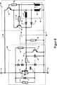
不可欠な要素として図2に示す保護回路装置は、スイッチ手段30の構成要素であるMOS電界効果トランジスタ1を含むが、これについてより詳細に後述する。接続部11及び12の間には電流路若しくは切替え路としてのドレイン−ソース路が存在し、接続部11及び12は太陽電池モジュールの太陽電池の直列回路に接続している。通常動作時には、ドレイン−ソース路には20Vの正電圧が存在するが、陰になった場合には、0.6Vの負のドレインーソース電圧となる。MOSFET1固有のボディダイオードを参照番号2に示す。分離回路40は、一方ではMOSFET1のドレイン接続に接続し、他方では供給回路及び/又は充電回路50(以下では充電回路と称する)に接続する。なお分離回路40は通常動作時には約20Vまでの正のドレイン−ソース電圧をブロックしなければないが、陰になった場合には、0.6V以下という低い負の電圧を、後続の充電回路50へと可能な限り損失を生じないように導く必要がある。
As an indispensable element, the protection circuit device shown in FIG. 2 includes the MOS
充電回路50は、陰になった場合には分離回路40の後方で利用できる低い負の直流電圧を変換して、MOSFET1の起動及び/又は更なる回路部分の供給に必要な、より高い正の電圧とする。よって、チョークコイル又は変圧器におけるエネルギーの中間的な貯蔵手段というだけでなく、充電ポンプを容量的に動作することに基づく概念を適用できる。なお、この好適な実施形態については後述する。変換した電圧は、キャパシタとも称するエネルギー貯蔵手段60に中間的に貯蔵するが、特に有利にはMOSFET1のゲートキャパシタンスを直接エネルギー貯蔵手段として利用する。
The charging
MOSFET1のゲート電極Gはタイマスイッチ80によって時間に依存して起動されるが、MOSFETは電力損失を減少するべくサイクルタイムの最大部分にわたって起動され、場合によってはより短い期間にわたって線形的に動作し、またより短い期間にわたって完全にブロックされる。MOSFET1のバイパス電流はボディダイオード2を通って流れる。図3、図6、及び図7、ならびに図5による保護回路では、MOSFETのゲートキャパシタンスは最初の2つの時間範囲では放電されるが、最初の時間範囲の終了時には充電回路を介して充電される。図8による保護回路では、図9に示すように放電が時間領域2及び3においてのみ実行され、時間領域4の終了時には、充電回路を介してキャパシタンスが再び充電される。
The gate electrode G of the
好ましくは、コンパレータ70を設けてドレイン−ソース電圧を監視するようにし、コンパレータ70は、許容できる状況の場合には、タイマ回路の信号も同様に取得する論理回路90に信号を送る。コンパレータ70の監視基準としては、例えば極性のほかにMOSFET1のドレイン−ソース電圧の大きさがある。供給回路若しくは充電回路50に、そして全ての他の回路にも同様に接続したドライバ回路100は、論理回路の信号に依ってMOSFET1のゲートを制御する。
Preferably, a
図2に示す機能ブロックは、概観をより見やすくするように示しているが、さらなる実施形態の例では、全ての機能ブロックが必ずしも別個に存在する必要はなく、またいくつかの機能ブロックをまとめて1つの要素としても良いことを理解されたい。 The functional blocks shown in FIG. 2 are shown to make the overview easier to see, but in the example of further embodiments, not all functional blocks need to exist separately, and several functional blocks are grouped together. It should be understood that it may be a single element.
本発明による保護回路装置の第1の実施形態例に関して、構成要素を個別に示した状態で図3に示す。なお、この図では機能ブロックについて部分的に破線を使って示している。以前にも説明したスイッチ手段30は、ボディダイオード2を備えるMOSFET1の他に、固有のゲートキャパシタンス3を含む。第1ツェナーダイオード7は、接続部12に接続した基準電位リードによって順方向においてゲート接続に接続する。このダイオードは、ゲート電圧を例えば15Vという許容可能な値に制限するよう作用する。電流路を有するトランジスタ9は基準電位32とゲート制御リード31の間に接続し、このトランジスタのベースは高インピーダンス抵抗10を介してMOSFET1のドレイン接続に接続する。トランジスタ9の電流路に平行にさらなるキャパシタ8が存在し、直列抵抗6はキャパシタ8と第1ツェナーダイオード7の間で制御リード31にて接続する。ドレイン接続とゲート制御リード31の間にはダイオード13と第2ツェナーダイオード14が存在する。
The first embodiment of the protection circuit device according to the invention is shown in FIG. 3 with the components individually shown. In this figure, functional blocks are partially shown using broken lines. The previously described switch means 30 includes an
MOSFET1固有のボディダイオード2に平行にさらなるダイオード4を配置するが、このダイオードはMOSFET1がオンにならない場合にバイパス電流の一部若しくは全部を導く。
A further diode 4 is placed in parallel with the
例えばバリスタ若しくはトランスゾーブ(trans−zorb)ダイオードのような過電圧保護素子5をMOSFET1に平行に配置し、極めて高く短い電圧インパルスを制限する。
For example, an
固有のボディダイオード2を有するMOSFETは、この保護回路によってドレイン−ソース路及びゲート−ソース路における高すぎる電圧から保護される。さらに、通常動作への移行時、即ちドレイン−ソース電圧が正となる場合には、迅速にオフとなることが必要であり、さらには通常動作時にはMOSFETが意図せずオンとなることを防止すべきである。
The MOSFET with its
ドレイン−ソース電圧が正となる場合、即ち通常動作への移行時には、トランジスタ9が高インピーダンスベース直列抵抗10を介して完全に起動され、低インピーダンス直列抵抗6を介して非常に迅速にMOSFET1のゲートキャパシタンス3を放電する(正帰還)。トランジスタは通常動作時には直列抵抗6にかかるゲート−ソース電圧を約0Vに保ち続ける。これにより、例えば外部からゲート電圧が生じることによって意図せずオンに切り替わることが確実に防止される。ベース直列抵抗10を介して流れる無駄な電流は、通常動作時には無視できるほど小さいものである。
When the drain-source voltage is positive, i.e. when transitioning to normal operation, the transistor 9 is fully activated via the high impedance
基本的に、MOSFETにはある程度のアバランシェ耐量がある。即ち、短い間で最大許容ドレイン−ソース電圧を越える、即ち60Vより大きい電圧になると、MOSFETに指定された電圧は40Vであることから、MOSFETは導電性となって、損傷を負うことのないようにピーク電圧を制限する。このような動作タイプであれば、信頼の置ける動作範囲を考慮しなくてもよく思えるが、これでは構成要素へのストレスが増大してしまう。このため、超過の電圧が発生すると目的どおりにそのゲートソース路を介して、即ちツェナーダイオード14及びダイオード13を介してMOSFETが起動され、ツェナーダイオード4のツェナー電圧を越えると、ゲートの電位が上昇して正の電位となり、MOSFET1が線形範囲で動作する。トランジスタ9が導電となった場合に正のゲート電圧を構築することができるようにするために、直列抵抗9が必要である。
Basically, a MOSFET has a certain amount of avalanche resistance. That is, if the maximum allowable drain-source voltage is exceeded in a short period of time, that is, the voltage exceeds 60V, the voltage specified for the MOSFET is 40V, so that the MOSFET becomes conductive and will not be damaged. Limit the peak voltage to With such an operation type, it may not be necessary to consider a reliable operation range, but this increases the stress on the components. For this reason, when an excessive voltage is generated, the MOSFET is started through its gate source path, that is, through the Zener diode 14 and the
固有のゲートキャパシタンス3に直列抵抗6を介して平行に接続すると共に、ゲートキャパシタンス3より大きい容量を有することが一般的なキャパシタ8により、回路の障害傾向が減少する。キャパシタは、直列抵抗6のゲートから遠い側に接続することが有利であるが、これは一時的に過電圧となった場合にツェナーダイオード4及びダイオード13を介して比較的低いゲートキャパシタンス3のみを充電するだけでよいためである。
Capacitors 8 that are connected in parallel to the
上述のように、分離回路40は通常動作時には20Vの正のドレイン−ソース電圧を後続の回路から分離するという働きを有し、陰になった場合には、0.6Vという負のドレイン−ソース電圧を後続の回路部分に導く働きを有する。図3で示す分離回路40は、自己導電性のnチャネル接合(J−FET)28を含み、このJ−FETのソース電極はMOSFET1のドレイン接続に接続し、またJ−FETのドレイン電極は後続の供給回路若しくは充電回路50に接続し、ゲート電極は高インピーダンスゲート抵抗29を介して基準電位リード32に接続する。この抵抗29は、陰になった場合のように正のゲート−ドレイン電圧又はゲート−ソース電圧が0.5Vより大きくなった場合に、ゲートダイオードを通る電流を制限する。ブロックするために、低インピーンダンスJ−FET28にはドレインだけでなくソースに対しても約5Vの負のゲート電圧が必要である。これは、通常動作時にソース−ゲート路に対しては直接行われる。それとは対照的に、ドレイン−ゲート路に対しては、ドレイン電位を正の値と見込んだ場合にのみ行われ得る。このためには、後続の供給回路及び充電回路50がJ−FETの閾値電圧の大きさの逆電圧、即ち約5Vの電圧を受け入れるようにする必要がある。この特定の特徴は以下の後述する充電回路50によって保証される。
As described above, the
前述したJ−FET28ではなく、自己導電性MOSFETを使用することもできる。これは同様の働きを有するものであるが、抵抗29を介して電流を制限する必要がない。これは典型的にゲート絶縁を±20Vとすることができるためである。
Instead of the J-
供給回路及び/又は充電回路50は0.6Vの負の入力電圧を、MOSFETを起動させるのに十分な15Vという正の出力電圧に変える働きを有している。MOSFET1のボディダイオード2における電圧降下を考慮しながら、0.4Vより小さい電圧でも確実に開始することを保証しなければならない。この電圧降下は温度の上昇と共に減少し、分離回路40において電圧の降下を生じる可能性がある。充電回路は非常に頑丈でなければならないが、作製に手間がかかってはならない。コンパレータ70の機能ばかりでなく、図2のタイマ回路80及びドライバ回路100の機能についても部分的に想定しなければならない。
The supply circuit and / or charging
図3による充電回路50は、エミッタ回路24において動作されるトランジスタ24を含み、そのエミッタはJ−FET28のドレイン接続に接続し、そのコレクタは変圧器20の一次巻線21に接続する。トランジスタ24のベースは直列抵抗25を介して正帰還巻線22に接続する。出力巻線21'は一次巻線21と直列に存在し、変圧器20は自動変圧器として接続される。トランジスタ24のコレクタは、一次巻線21と出力巻線21'との間に接続する。出力巻線21'は、整流ダイオード23と直列レジスタ6を介してゲートキャパシタンス3に接続する又は付加的なキャパシタ8に直接接続する。更なるダイオード23'は一次巻線の終端を付加的なキャパシタ8に接続する。
The charging
さらに、充電回路50はトランジスタ26を含み、このトランジスタのエミッタはJ−FET28のドレイン接続に接続し、そのコレクタはダイオード3と直列抵抗6の間に接続し、そのベースは直列抵抗27を介して正帰還巻線22の接続部に接続する。
Further, the charging
タイマ回路80'の構成要素であり得る放電抵抗81は、基準電位リード32とゲート制御リード31の間に接続する。
A
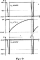
機能、特に供給回路若しくは充電回路の機能と、MOSFET1の切替え作用について、図4及び図5の時間に依存した電圧経過を参照しながら説明する。陰が生じ、MOSFET1がオンになる状況では、MOSFET1のオン切替え抵抗(RDSon)と一時的な太陽発電電流に依って、数ミリボルト、例えば−30mVの負の電圧がドレイン−ソース路において降下する。これを図4の領域(1)に示す。分離回路40を介して提供される電圧が十分ではないため、供給回路50は動作しない。放電抵抗81は例えば100ms(領域(1))以内でゆっくりとMOSFET1のゲートキャパシタンス3を放電するが、この時MOSFET1は図4に示すように例えば15Vに充電されている。MOSFET1の閾値電圧が例えば5Vのゲート−ソース電圧に到達すると、完全なる起動状態領域から線形領域(領域(2))に移行し、図4に示すようにドレイン−ソース電圧がゆっくりと上昇する。以下にさらに述べることになるが、充電回路50を介してゲート−ソースキャパシタンス3を再充電しなければ、MOSFET1は完全にブロックされた状態になり、この場合約0.4Vから約1Vの負の電圧降下を伴って、太陽発電電流がボディダイオード2を通って完全に流れる。
The function, particularly the function of the supply circuit or the charging circuit, and the switching action of the
リード34と基準電位リード32との間、即ち分離回路40のドレイン接続において約0.3Vから0.4Vの電圧が存在する場合には、顕著なコレクタ電流と変圧器20の一次巻線21を通る電流を生じるために、トランジスタ24において適切な大きさのベース電流が流れる。これにより、正帰還巻線22に電圧が生じるが、これは巻線方向のためリード32と34の間の電圧に加算され、ベース電流が増幅されることとなり、これによって迅速な移行が始まる。トランジスタ24は完全に導電性となり、一次巻線21のインダクタンスと一次巻線において有効な電圧とによって一次電流が一時的に増大するが、これはリード32と34の間で有効な電圧に相当する。
If there is a voltage of about 0.3V to 0.4V between the lead 34 and the reference
変圧器20の中心が飽和状態になった場合、又はトランジスタ24のベース電流が完全な起動を行うには不十分となった場合、正帰還が逆転し、トランジスタ24が突然ブロックされる。変圧器のインダクタンスに蓄積されたエネルギーは、一次巻線21と出力巻線21'とを介してゲートキャパシタンス3に移行するだけでなく、付加的なキャパシタ8にも移行する。このことは、図4及び図5の領域(3)の終了時又は領域(1)の開始時に確認できる。よってMOSFET1はオンとなり、上述のように内部抵抗によって数ミリボルトの負の電圧降下が生じるだけである。充電回路50には電圧が適切に供給されず、動作しない。変圧器20はエネルギーを十分に蓄積できる大きさあり、既に1つの変圧器クロックを備えており、例えば15Vという通常の値にゲートキャパシタンス3若しくはキャパシタ8を充電する。
If the center of the
実際の変圧器では、トランジスタ24が急にオフとなった場合に変圧器巻線21において回避できない漏出が誘発されることにより、トランジスタ24において過電圧ピーク24となり、これによってトランジスタ24が損傷を受ける可能性がある。ダイオード23'はこのピークを防止することができるが、これはオフとなった瞬間にダイオード23'が変圧器巻線に電流を流し、この電流が充電されていないキャパシタにさらに流れることとなるためである。
In an actual transformer, if
ここで再度、常に「クロック」は充電回路50に対して使用し、「サイクル」は常に全体の回路に対して使用することとする。充電サイクルは2つの段階を含む:第1段階は上述したものであって、完全な全サイクルの領域(3)に始まり、領域(3)の持続時間にわたって続く。迅速な移行自体にかかる時間は数μsにすぎず、時間の実質的な部分は領域(3)が終了するまでの電流の「ゆっくりとした」上昇にある。第2クロック段階は、エネルギーが変圧器からキャパシタンスへと移行される際に始まる。この工程は下降側面に従って部分的に領域(3)と後続サイクルの領域(1)に存在する。しかし、この過充電は全体でも数μs持続するのみである。
Here again, the “clock” is always used for the charging
機能に関して上述したことから明らかなように、切替え機能の他に、ベース−エミッタ路を備えるトランジスタ24は図2のコンパレータ70の機能を担う。即ち、トランジスタ24は大きすぎるドレイン−ソース電圧がかかっている場合のみ動作する。有利には、トランジスタ24をMOSFET1に熱的に連結する。両構成要素はシリコン技術に基づいているため、全温度で回路を安全に機能させることを保証するべく、ボディダイオードとベース−エミッタダイオードの順電圧の方向を同じとする。
As is clear from the above description regarding the function, in addition to the switching function, the
MOSFETの負のドレイン−ソース電圧、又は充電回路50に提供される電圧が、例えば分離回路40の内部抵抗のためにさほど大きくない場合、上述の迅速な移行又は領域によって規定される変圧器クロックは、完全にその過程をたどる必要はない。よって、特に太陽発電電流が小さい場合には、キャパシタ8又はMOSFET1のゲートキャパシタンス3は十分には充電されない。
If the negative drain-source voltage of the MOSFET or the voltage provided to the charging
保護回路装置の安定した動作をさらに保証するために、迅速な移行が始まった際に、トランジスタ26を介してMOSFET1のゲートを極めて迅速に放電させることで、トランジスタ26がオンとなるが、これは図5の領域(3)から確認できる。MOSFET1は一瞬にしてブロックし、図4に示すようにドレイン−ソース電圧が、迅速な移行の閾値である約−0.4Vから、ボディダイオード2の順電圧である約−0.6Vへと非常に素早く上昇する。従って、さらなる正帰還がトランジスタ26により生じる。変圧器クロックの第2段階では、トランジスタ26は正帰還巻線22における負の電圧を介して完全にブロックされ、これによりゲートキャパシタンス3若しくはキャパシタ8が充電され得る。
In order to further guarantee the stable operation of the protection circuit device, the
図3、図4、及び図5による回路の全サイクルは、MOSFET1が完全に起動される第1の長い段階(100ms)と、MOSFET1が線形領域に入り、ドレイン−ソース電圧が約−0.4Vへとゆっくりと上昇する第2のより短い段階(20ms)と、MOSFET1が正帰還回路によって短い時間(例えば1ms)の間完全にオフとなる第3のより短い段階とを含む。しかし、第2段階と第3段階において上昇する熱量に関しては全く問題がなく、従来の方法でも逃がすことが可能である。
The entire cycle of the circuit according to FIGS. 3, 4 and 5 is the first long phase (100 ms) when
数回にわたって既に述べたように、モジュールの通常動作時にはMOSFETのドレイン−ソース電圧は約15Vから約20Vの正の値に上昇する。分離回路40に設けたJ−FET28がブロックするために、そのドレイン接続ばかりでなくソース接続についてもゲート接続に対して約5Vの正の値とならなければならず、そうでない場合には、許容不可能な漏れ電流が充電回路50に流れ込む。図3に示す回路では正の電圧に対するトランジスタ24及び26のエミッタ−ベース路がブロックした方向におけるリード34に存在し、それらは約5Vまでの逆電圧を受け入れることができるため、J−FET28のドレイン電位は5Vに上昇することとなり、これにより必要に応じてJ−FET28を完全にブロックする。
As already mentioned several times, during the normal operation of the module, the drain-source voltage of the MOSFET rises from about 15V to a positive value of about 20V. In order for the J-
図6に更なる実施形態の例を示すが、これは図3に示す回路を簡略化したもので、分離回路40の機能と、供給回路若しくは充電回路50のトランジスタ24の機能を1つのグループとしている。別の方法で、図3による回路と図4及び図5による電圧図を適用することができる。
FIG. 6 shows an example of a further embodiment, which is a simplification of the circuit shown in FIG. 3, in which the function of the
理解されるように、トランジスタ24の動作は逆となる。バイポーラトランジスタにおいてエミッタとコレクタをかえると基本的なトランジスタの特徴は保持されるが、動作が逆となり電流の増幅がおおよそ30%程度減少する。この特徴は、適切に低いインピーダンスのベース直列抵抗25によって考慮される。実際、状況によっては正帰還巻線22のオーム抵抗は電流を制限するのに既に十分であるため、構成要素25を設ける必要がない。トランジスタ24動作が逆になるということには、そのベース及びエミッタは直流電圧に対して基準電位32に存在しており、コレクタ回路において太陽電池モジュールの通常動作時に動作されるという大きな利点が伴う。トランジスタはこの動作モードにおいて何ら問題なく20Vの発生電圧を受け入れることができ、電圧に対して耐性のあるトランジスタタイプを適用することもでき、これによって超過の電圧パルスに対しても耐性が増す。供給回路若しくは充電回路の発振は、この動作の場合には正帰還巻線が帰還として作用するため、除外できる。
As will be appreciated, the operation of
トランジスタ26は通常通りに動作し続け、その機能は図3のものに相当する。しかしそのエミッタはトランジスタ24のエミッタに接続する。これにより、トランジスタ24の接続状況において、トランジスタ26を介してMOSFET1のゲートを迅速に放電することができ、このタイプの回路では、MOSFET1の導電段階とモジュールの通常動作時に負の逆電圧を受け入れる必要がない。
The
上述のように、図3及び図6に対応する回路では、ゲートキャパシタンス3若しくはキャパシタンス8を充電するのに必要なエネルギーは、単一クロックパルスにおいて、即ちトランスデューサ変圧器20及びトランジスタ24の1回の迅速な移行の際に送られる。しかし充電回路は数回のクロックパルスにおいてエネルギーを送ることができ、MOSFET1のゲートキャパシタンス若しくはエネルギー貯蔵手段が、数回のクロックパルスにおいて充電され、スイッチがオフとなる。
As described above, in the circuit corresponding to FIGS. 3 and 6, the energy required to charge the
最終的に、前述のゲートキャパシタンス又はキャパシタ8の不完全な充電工程は、MOSFET1の永久的な線形領域を達成するように、原則として例えばベース直列抵抗25の大きさを適切に採ることによって発生する。この動作モードでは、トランジスタ24はドレイン−ソース電圧に対する調整手段として作用する。これによってMOSFET1は完全には起動されないが、トランジスタ24を介して線形動作における調整手段として保持される。よって、陰になった場合にはドレイン−ソース路において約0.3Vから0.4Vの負の電圧が降下するが、これは供給回路又は充電回路50を連続して動作させるのに十分である。この考えによれば、MOSFET1における損失はMOSFETを通して完全に接続した場合より大きくなる。しかし、このように線形的にMOSFETが動作することにより太陽発電電圧若しくは太陽発電電流が急上昇することがない。
Finally, the incomplete charging process of the aforementioned gate capacitance or capacitor 8 occurs in principle by taking the size of, for example, the
MOSFET1において発生する電力損失をさらに減少するために、図4及び図5の領域(2)に対応するMOSFETの線形領域における一時的な動作を防止することができる。かかる回路を図7に示すが、この回路は図3又は図6による回路とは80''に示す放電回路の点で異なっている。図3及び図6による回路の場合、MOSFET1がオフとなる時点は、そのゲートキャパシタンス3、場合によって存在するキャパシタ8、並びに放電抵抗81によって形成される時間的要因によって決まる。放電抵抗81の代わりに、非線形的に動作する能動ゲート放電回路を適用する。これは、所定の閾値電圧より高い高インピーダンスを有するが、閾値電圧に届かないかなり低いインピーダンスを有するという特徴を備える。この特徴を有する回路は、例えばシュミットトリガ回路により具現化することができる。このトリガ回路の迅速な移行点、即ちゲート放電回路80''の迅速な移行閾値が、MOSFETの完全な起動に必要な最も高いゲート電圧より高く、例えば6V以上適用される場合には、充電回路50による充電の後まず迅速に減少し、新たな充電クロックパルスがトリガされる。図4及び図5で領域(2)に示す線形領域におけるMOSFET1の動作は回避され、かかる回路により電力損失がさらに減少する。
In order to further reduce the power loss generated in the
この回路80''により、ゲート制御リード31と基準電位リード32との間に小信号MOSFET87を接続するが、そのゲート接続はトランジスタ83のコレクタに接続し、エミッタは基準電位32に存在する。ベース接続は、ゲート制御リード31と基準制御リード32の間の電圧分配手段84、85に接続する。最終的に抵抗86は、リード31とMOSFET87のゲート接続との間に接続する。キャパシタ88は、トランジスタ83のコレクタ接続から帰還巻線22にキャパシタ88を接続する。
With this
MOSFET1の高いゲート電圧により、トランジスタ83は電圧分配手段84、85を介して完全に起動される。従って、そのコレクタ電位とMOSFET87のゲート電位は基準電位32に近くなるため、MOSFET87がブロックされる。
Due to the high gate voltage of the
MOSFET1のゲートキャパシタンス3並びにキャパシタ8は、高インピーダンス抵抗84、85、及び86を介してゆっくりと放電される。MOSFET1のゲート電圧が最小値より低くなった場合には、トランジスタ83がブロックし始め、MOSFET87のゲート電圧が上昇する。例えば約1から2Vの閾値電圧が小信号MOSFET87によって達成されると、そのドレイン−ソース電圧は低インピーダンスとなり、ゲートキャパシタンス3若しくはキャパシタ8が迅速に放電される。これによってトランジスタ83に対するベース電流はさらに減少し、迅速な移行が開始される。この迅速な移行は、MOSFET1の所定のドレイン−ソース電圧から、供給回路若しくは充電回路50が上述のように動作し始めることで促進される。よって、正帰還巻線22における電圧が第1のクロックパルス区分において上昇して正の値となる。この上昇が結合キャパシタ88を介してMOSFET87のゲートに移行されることで、正帰還工程が再度強化され、ゲートキャパシタンス3又はキャパシタ8が完全に放電される。MOSFET1はこれによって非常に迅速に完全にブロックされる。
The
トランジスタ26及び直列抵抗27における正帰還分岐については、キャパシタ88を介した正帰還が付加されるため、なくすことが可能である。
The positive feedback branch in the
充電クロックパルスの第2段階では、キャパシタ88によって移行された正帰還巻線22において負の電圧が急上昇することを介して、MOSFET87が完全にブロックされることにより、ゲートキャパシタンス3若しくはキャパシタ8が再び充電され得る。
In the second stage of the charge clock pulse, the
図8は、保護回路の特に有利な更なる設計を示している。この図は、図6の回路に本質的には対応しているが、トランジスタと直列抵抗10がなく、受動放電回路80'の代わりに能動放電回路80'''が設けられている。
FIG. 8 shows a particularly advantageous further design of the protection circuit. This figure essentially corresponds to the circuit of FIG. 6, but without the transistor and
能動放電回路80'''の重要な点は、自己導電性J−FET81'である。一方で回路80'''は、太陽電池の通常動作時に直列抵抗6と変圧器の巻線21'及び21を介してMOSFET1のゲートを基準電位リード32に接続する点で、トランジスタ9並びに直列抵抗10の代わりとなる。これにより、外部で生じたゲート電圧によりMOSFET1が意図せずオンとなったり、ダイオード12及び14の漏れ電流が生じたりすることが確実に防止される。他方では、図9に示すようにMOSFET1の最適な起動が可能となることで、バイパススイッチ素子における電力損失がさらに減少することとなる。
An important point of the
前述の回路とは対照的に、図8の回路では、MOSFET1のゲートが充電工程後の抵抗によって放電されないが、図9に示すようにゲート電圧UGSは、期間1の間その全値を保持する。よって、この時のMOSFETのインピーダンスは非常に低く、従って電力の損失も低い。キャパシタ82'及び抵抗84'によって形成されるタイマの時定数により、MOSFET1がオフになる時点が決定する。期間4の終了時におけるキャパシタ8及び3の充電段階では、キャパシタ82'は、3本の巻線21、21'、及び22における電圧の合計、本例では17.5Vにダイオード83'を介して充電される。巻線21及び21'の電圧が変圧器20の消磁後にゼロに戻ると、J−FET81'のゲートにおける電位は−17.5Vの値になる。これでJ−FETは完全にブロックされ、理想的な場合にはキャパシタ8及び3からの電荷の流出はない。キャパシタ82'は抵抗84'を介して、例えば100ms以内でゆっくりと放電される。J−FET81'のゲート電圧がその閾値電圧(本例では−2V)に到達すると、J−FETは低インピーダンスとなり、巻線21'及び21を介してキャパシタ8及び3を放電することにより、MOSFET1のゲート電圧UGSが急激に降下する。これを図9の時間区分2で示す。この電圧がMOSFET1の閾値電圧に達しない場合にはMOSFET1がブロックし始め、ドレイン−ソース電圧UDSは図9の時間区分3で示すように迅速に上昇する。約−0.4Vの値に達すると、前述の回路の場合に述べたようにトランジスタ26を介したキャパシタ8及び3の急速な更なる放電と共に、充電回路50の迅速な移行が始まる。時間区分4では、トランジスタ24が完全に導電性となり変圧器20にエネルギーが蓄積される。この区分の終了時にはキャパシタ8及び3だけでなく82'も再び充電される。
In contrast to the circuit described above, in the circuit of FIG. 8, the gate of
図8の回路の電力損失は、MOSFET1がサイクル時間のより長い部分に対して完全に起動されることにより、他の回路に比べてさらに減少し、ブロック状況におかれる期間はサイクル時間の1%未満となる。
The power loss of the circuit of FIG. 8 is further reduced compared to the other circuits by the
当然のことながら、上述の回路は全て相補型半導体タイプと共に構成することができる。 Of course, all of the circuits described above can be configured with complementary semiconductor types.
低損失のバイパス素子としての機能とは別に、MOSFET1の付加的な機能としては、検査や火災の場合に、設備における太陽発電電圧の短絡回路として想定できる。このために、例えば制御リードを介して、太陽発電機内の全てのMOSFETのゲート接続に制御電圧をかけて、各モジュールの電圧を短絡させる。このため、危険を伴わない充電部と太陽発電機へのリードとの接触が可能となる。
Apart from the function as a low-loss bypass element, an additional function of the
1 MOSFET
2 ボディダイオード
30 スイッチ手段
40 分離回路
50 供給回路又は充電回路
60 エネルギー貯蔵手段
70 コンパレータ
80 タイマスイッチ
90 論理回路
100 ドライバ
1 MOSFET
2
Claims (24)
バイパス素子として作用し、その電流路が前記複数の太陽電池に並列に接続し得る、少なくとも1つの制御可能な電気スイッチ素子と、
前記バイパス素子の制御電極を起動させる制御電圧を生成する供給回路と、
通常動作時には前記バイパス素子の前記電流路にかかる電圧を前記供給回路に対してブロックし、陰になった場合には少なくとも1つの太陽電池の前記電流路にかかる電圧を供給電圧に切り替える分離回路と、
を含むことを特徴とする保護回路装置。A protection circuit device for a solar cell module in which a plurality of solar cells are connected in series, including a device that operates in normal operation and a device that operates simultaneously when shaded,
At least one controllable electrical switch element that acts as a bypass element, the current path of which can be connected in parallel to the plurality of solar cells;
A supply circuit for generating a control voltage for activating the control electrode of the bypass element ;
A separation circuit that blocks the voltage applied to the current path of the bypass element to the supply circuit during normal operation, and switches the voltage applied to the current path of at least one solar cell to the supply voltage when shaded. ,
A protective circuit device comprising:
を特徴とする請求項1に記載の保護回路装置。Designing the supply circuit as a charging circuit for the energy storage means to convert the voltage available when shaded into a higher voltage and activate the controllable bypass element;
The protection circuit device according to claim 1.
を特徴とする請求項1又は2に記載の保護回路装置。Designing the controllable bypass element as a MOS field effect transistor;
The protection circuit device according to claim 1 or 2.
を特徴とする請求項2又は3に記載の保護回路装置。Designing the energy storage means as an inherent capacitance and / or capacitor of the controllable bypass element;
The protection circuit device according to claim 2 or 3.
を特徴とする請求項1から4のいずれか一項に記載の保護回路装置。 Designing the isolation circuit as a field effect transistor ;
The protection circuit device according to claim 1, wherein:
を特徴とする請求項1から4のいずれか一項に記載の保護回路装置。Designing the isolation circuit as a bipolar transistor for reverse operation;
The protection circuit device according to claim 1, wherein:
を特徴とする請求項2に記載の保護回路装置。A timer circuit for setting a time cycle, said controllable bypass element is in the second time domain with the first time domain is completely connected completely blocked, the energy storage means is a second Being charged in the time domain of
The protection circuit device according to claim 2 .
を特徴とする請求項7に記載の保護回路装置。The time cycle includes a third time region that exists between the first time region and the second time region, wherein the controllable bypass element operates in a linear state in the third time region. Being
The protection circuit device according to claim 7.
を特徴とする請求項2に記載の保護回路装置。The supply circuit or charging circuit comprises adjustment circuit, the said controllable bypass device by adjusting circuit can be operated continuously in a linear state,
The protection circuit device according to claim 2 .
を特徴とする請求項2に記載の保護回路装置。The supply circuit or charging circuit boosts the voltage available to the transformer, or at least one coil, or shade, to generate the voltage necessary to activate the controllable bypass element Including at least one capacitor for intermediately storing energy for
The protection circuit device according to claim 2 .
を特徴とする請求項2に記載の保護回路装置。The supply circuit or charging circuit includes a charge pump for boosting the voltage available in the event of a shadow to generate the voltage necessary to activate the controllable bypass element;
The protection circuit device according to claim 2 .
を特徴とする請求項2に記載の保護回路装置。The supply circuit includes a transformer including a positive feedback winding and a first electronic switch element , wherein the first switch element and the transformer perform a quick transition similar to a self-blocking oscillator means, Energy stored in the transformer is sent to the energy storage means ;
The protection circuit device according to claim 2 .
を特徴とする請求項12に記載の保護回路装置。 The first electronic switch element performs the reverse operation to simultaneously form the separation circuit ;
The protection circuit device according to claim 12.
を特徴とする請求項12又は13に記載の保護回路装置。Connecting an additional output winding , similar to an automatic transformer, in series with the primary winding ,
The protection circuit device according to claim 12 or 13, characterized in that:
を特徴とする請求項14に記載の保護回路装置。 The current path of the first switch element is in series with the primary winding, and the positive feedback winding is connected to the control electrode of the first switch element ;
The protection circuit device according to claim 14 .
を特徴とする請求項1から15のいずれか一項に記載の保護回路装置。Selecting the time constant of the first discharge circuit such that the control electrode of the controllable bypass element is connected to the first discharge circuit and the ratio of the conduction time of the bypass element to the non-conduction time is increased ;
The protection circuit device according to any one of claims 1 to 15, wherein
を特徴とする請求項16に記載の保護回路装置。Wherein the first discharge circuit, connected in parallel to the bypass device specific capacitance, or, connected in parallel to a capacitor connected in parallel to the inherent capacitance, have a resistance,
The protection circuit device according to claim 16.
を特徴とする請求項12から17のいずれか一項に記載の保護回路装置。The supply circuit includes a rapid discharge circuit , and the discharge circuit quickly discharges the inherent capacitance at the beginning of a rapid transition, or quickly discharges an additional capacitor connected in parallel to the inherent capacitance. To do,
The protection circuit device according to claim 12, wherein:
を特徴とする請求項18に記載の保護回路装置。The rapid discharge circuit comprises a second electronic switch element, the second electronic switching element, which has a control electrode connected to said positive feedback winding, in parallel with the switch of the prior SL first electronic switch element Or having a current path from the connection portion of the control electrode of the bypass element , which exists in series,
The protection circuit device according to claim 18.
を特徴とする請求項16に記載の保護回路装置。 The first discharge circuit is designed as a non-linearly active active discharge circuit having a high impedance higher than a threshold voltage and a low impedance lower than the threshold voltage, and the bypass switch element is completely activated at its control electrode Determining the threshold voltage according to the voltage required for
The protection circuit device according to claim 16.
を特徴とする請求項20に記載の保護回路装置。Designing the first discharge circuit as a Schmitt trigger circuit;
The protection circuit device according to claim 20.
を特徴とする請求項16に記載の保護回路装置。 The first discharge circuit includes a self-conductive J-FET, a network of a diode , a capacitor , and a discharge resistor , so that a time factor that periodically turns off the bypass element after a predetermined time has elapsed. Is formed,
The protection circuit device according to claim 16.
を特徴とする請求項1から22のいずれか一項に記載の保護回路装置。Assigning the controllable bypass element to a protection circuit against overvoltage and unintentionally turning on;
The protection circuit device according to any one of claims 1 to 22, wherein:
を特徴とする請求項1から23のいずれか一項に記載の保護回路装置。Applying a voltage on the control electrode of the bypass element to electrically switch the bypass element in order to short-circuit the solar cell module for inspection purposes or in case of fire,
The protection circuit device according to any one of claims 1 to 23.
Applications Claiming Priority (5)
| Application Number | Priority Date | Filing Date | Title |
|---|---|---|---|
| DE102005024428.9 | 2005-05-24 | ||
| DE102005024428 | 2005-05-24 | ||
| DE102005036153.6 | 2005-07-25 | ||
| DE102005036153A DE102005036153B4 (en) | 2005-05-24 | 2005-07-25 | Protection switching device for a solar module |
| PCT/EP2006/005051 WO2006125664A1 (en) | 2005-05-24 | 2006-05-23 | Circuit breaker for a solar module |
Publications (3)
| Publication Number | Publication Date |
|---|---|
| JP2008546183A JP2008546183A (en) | 2008-12-18 |
| JP2008546183A5 JP2008546183A5 (en) | 2009-06-25 |
| JP4999839B2 true JP4999839B2 (en) | 2012-08-15 |
Family
ID=36838691
Family Applications (1)
| Application Number | Title | Priority Date | Filing Date |
|---|---|---|---|
| JP2008512777A Active JP4999839B2 (en) | 2005-05-24 | 2006-05-23 | Protection circuit device for solar cell module |
Country Status (8)
| Country | Link |
|---|---|
| US (1) | US7898114B2 (en) |
| EP (2) | EP1884008B1 (en) |
| JP (1) | JP4999839B2 (en) |
| CN (1) | CN101180781B (en) |
| AT (1) | ATE509415T1 (en) |
| DE (1) | DE102005036153B4 (en) |
| PT (1) | PT1884008E (en) |
| WO (1) | WO2006125664A1 (en) |
Families Citing this family (120)
| Publication number | Priority date | Publication date | Assignee | Title |
|---|---|---|---|---|
| DE102005036153B4 (en) * | 2005-05-24 | 2007-03-22 | Fraunhofer-Gesellschaft zur Förderung der angewandten Forschung e.V. | Protection switching device for a solar module |
| US10693415B2 (en) | 2007-12-05 | 2020-06-23 | Solaredge Technologies Ltd. | Testing of a photovoltaic panel |
| US11881814B2 (en) | 2005-12-05 | 2024-01-23 | Solaredge Technologies Ltd. | Testing of a photovoltaic panel |
| US8947194B2 (en) | 2009-05-26 | 2015-02-03 | Solaredge Technologies Ltd. | Theft detection and prevention in a power generation system |
| US9088178B2 (en) | 2006-12-06 | 2015-07-21 | Solaredge Technologies Ltd | Distributed power harvesting systems using DC power sources |
| US8013472B2 (en) | 2006-12-06 | 2011-09-06 | Solaredge, Ltd. | Method for distributed power harvesting using DC power sources |
| US9112379B2 (en) | 2006-12-06 | 2015-08-18 | Solaredge Technologies Ltd. | Pairing of components in a direct current distributed power generation system |
| US9130401B2 (en) | 2006-12-06 | 2015-09-08 | Solaredge Technologies Ltd. | Distributed power harvesting systems using DC power sources |
| US11888387B2 (en) | 2006-12-06 | 2024-01-30 | Solaredge Technologies Ltd. | Safety mechanisms, wake up and shutdown methods in distributed power installations |
| US8963369B2 (en) | 2007-12-04 | 2015-02-24 | Solaredge Technologies Ltd. | Distributed power harvesting systems using DC power sources |
| US8473250B2 (en) | 2006-12-06 | 2013-06-25 | Solaredge, Ltd. | Monitoring of distributed power harvesting systems using DC power sources |
| US11296650B2 (en) | 2006-12-06 | 2022-04-05 | Solaredge Technologies Ltd. | System and method for protection during inverter shutdown in distributed power installations |
| US8816535B2 (en) | 2007-10-10 | 2014-08-26 | Solaredge Technologies, Ltd. | System and method for protection during inverter shutdown in distributed power installations |
| US11309832B2 (en) | 2006-12-06 | 2022-04-19 | Solaredge Technologies Ltd. | Distributed power harvesting systems using DC power sources |
| US8618692B2 (en) | 2007-12-04 | 2013-12-31 | Solaredge Technologies Ltd. | Distributed power system using direct current power sources |
| US11728768B2 (en) | 2006-12-06 | 2023-08-15 | Solaredge Technologies Ltd. | Pairing of components in a direct current distributed power generation system |
| US11855231B2 (en) | 2006-12-06 | 2023-12-26 | Solaredge Technologies Ltd. | Distributed power harvesting systems using DC power sources |
| US11735910B2 (en) | 2006-12-06 | 2023-08-22 | Solaredge Technologies Ltd. | Distributed power system using direct current power sources |
| US11569659B2 (en) | 2006-12-06 | 2023-01-31 | Solaredge Technologies Ltd. | Distributed power harvesting systems using DC power sources |
| US11687112B2 (en) | 2006-12-06 | 2023-06-27 | Solaredge Technologies Ltd. | Distributed power harvesting systems using DC power sources |
| US8319483B2 (en) | 2007-08-06 | 2012-11-27 | Solaredge Technologies Ltd. | Digital average input current control in power converter |
| US8319471B2 (en) | 2006-12-06 | 2012-11-27 | Solaredge, Ltd. | Battery power delivery module |
| US8384243B2 (en) | 2007-12-04 | 2013-02-26 | Solaredge Technologies Ltd. | Distributed power harvesting systems using DC power sources |
| WO2008134366A1 (en) * | 2007-04-30 | 2008-11-06 | Bristol, Inc. | Intrinsically safe (is) solar panel |
| WO2009072076A2 (en) | 2007-12-05 | 2009-06-11 | Solaredge Technologies Ltd. | Current sensing on a mosfet |
| US8289742B2 (en) | 2007-12-05 | 2012-10-16 | Solaredge Ltd. | Parallel connected inverters |
| US11264947B2 (en) | 2007-12-05 | 2022-03-01 | Solaredge Technologies Ltd. | Testing of a photovoltaic panel |
| CN101933209B (en) | 2007-12-05 | 2015-10-21 | 太阳能安吉有限公司 | Release mechanism in distributed electrical power apparatus, to wake up and method for closing |
| US9291696B2 (en) | 2007-12-05 | 2016-03-22 | Solaredge Technologies Ltd. | Photovoltaic system power tracking method |
| US20090184746A1 (en) * | 2008-01-22 | 2009-07-23 | Microsemi Corporation | Low Voltage Drop Unidirectional Electronic Valve |
| US8111052B2 (en) | 2008-03-24 | 2012-02-07 | Solaredge Technologies Ltd. | Zero voltage switching |
| EP2294669B8 (en) | 2008-05-05 | 2016-12-07 | Solaredge Technologies Ltd. | Direct current power combiner |
| IT1390778B1 (en) | 2008-07-01 | 2011-09-23 | St Microelectronics Srl | ARCHITECTURE FOR CELL BY-PASS DIODE IN SERIES OF A PHOTOVOLTAIC PANEL |
| SG160241A1 (en) * | 2008-09-15 | 2010-04-29 | Alternative Energy Technology | Photovoltaic cell circuit |
| DE102008052037B3 (en) * | 2008-10-16 | 2010-04-08 | Moeller Gmbh | solar module |
| US20100108119A1 (en) * | 2008-11-17 | 2010-05-06 | Applied Materials, Inc. | Integrated bypass diode assemblies for back contact solar cells and modules |
| US8050804B2 (en) * | 2008-12-15 | 2011-11-01 | Array Converter, Inc. | Detection and prevention of hot spots in a solar panel |
| US8558103B2 (en) | 2009-01-28 | 2013-10-15 | Intersil Americas Inc. | Switchable solar cell devices |
| EP2430663A1 (en) * | 2009-05-12 | 2012-03-21 | Ramot at Tel-Aviv University Ltd. | System and method for controlling a group of photovoltaic generators |
| CN102422429B (en) | 2009-05-22 | 2014-08-06 | 太阳能安吉科技有限公司 | Electrically isolated heat dissipating junction box |
| US8169252B2 (en) * | 2009-07-09 | 2012-05-01 | Microsemi Corporation | Low voltage drop closed loop unidirectional electronic valve |
| CN102598287B (en) | 2009-08-26 | 2014-11-19 | 弗劳恩霍夫应用研究促进协会 | Bypass and protection circuit for a solar module and method for controlling a solar module |
| US8482156B2 (en) | 2009-09-09 | 2013-07-09 | Array Power, Inc. | Three phase power generation from a plurality of direct current sources |
| DE102009042084A1 (en) * | 2009-09-18 | 2011-06-22 | Gehrlicher Solar AG, 85609 | Low-maintenance electronic component to prevent backflow while protecting against overcurrents in photovoltaic systems |
| US8263920B2 (en) * | 2009-09-30 | 2012-09-11 | The Boeing Company | Diodeless terrestrial photovoltaic solar power array |
| US9324885B2 (en) | 2009-10-02 | 2016-04-26 | Tigo Energy, Inc. | Systems and methods to provide enhanced diode bypass paths |
| FR2951886B1 (en) * | 2009-10-23 | 2016-02-05 | Commissariat Energie Atomique | CONTROL WITH SLOWDOWN OF THE OPENING OF AN ELECTRONIC SWITCH |
| KR101025795B1 (en) * | 2009-12-30 | 2011-04-04 | 안현구 | Electrical charge relay enhancer and solar cell system including the enhancer |
| FR2955209B1 (en) * | 2010-01-12 | 2015-06-05 | Arnaud Thierry | SYSTEM FOR MANAGING AND CONTROLLING PHOTOVOLTAIC PANELS |
| JP4985795B2 (en) * | 2010-01-29 | 2012-07-25 | サンケン電気株式会社 | Solar power generation apparatus and solar power generation system |
| DE102010007495A1 (en) * | 2010-02-09 | 2011-08-11 | Wieland Electric GmbH, 96052 | Module bypass circuit for a photovoltaic module |
| US9425783B2 (en) * | 2010-03-15 | 2016-08-23 | Tigo Energy, Inc. | Systems and methods to provide enhanced diode bypass paths |
| IT1400922B1 (en) * | 2010-05-14 | 2013-07-02 | St Microelectronics Srl | BY-PASS DIODE OR CIRCUIT BREAKER FOR DC SOURCE MADE WITH A LOW RESISTANCE CONDUCTING MOSFET AND ITS SELF-POWERED CONTROL CIRCUIT WITH MEANS OF DISABLING THE DC SOURCE IN THE EVENT OF FIRE OR OTHER RISK |
| IT1400921B1 (en) | 2010-05-14 | 2013-07-02 | St Microelectronics Srl | BY-PASS DIODE OR SWITCH MADE WITH A LOW RESISTANCE CONDUCTING MOSFET AND ITS SELF-POWERED CONTROL CIRCUIT |
| DE102010023549B4 (en) * | 2010-06-03 | 2016-03-24 | Dmos Gmbh | Photovoltaic generator with circuit system and method for protecting photovoltaic modules |
| US8665575B2 (en) | 2010-06-25 | 2014-03-04 | International Business Machines Corporation | Solar module with overheat protection |
| DE102010036816A1 (en) * | 2010-08-03 | 2012-02-09 | Newtos Ag | Method and device for monitoring and controlling a photovoltaic system |
| TWI437601B (en) * | 2010-10-08 | 2014-05-11 | Nexpower Technology Corp | Solar module with bimetal breaker |
| US10230310B2 (en) | 2016-04-05 | 2019-03-12 | Solaredge Technologies Ltd | Safety switch for photovoltaic systems |
| US10673229B2 (en) | 2010-11-09 | 2020-06-02 | Solaredge Technologies Ltd. | Arc detection and prevention in a power generation system |
| GB2485527B (en) | 2010-11-09 | 2012-12-19 | Solaredge Technologies Ltd | Arc detection and prevention in a power generation system |
| US10673222B2 (en) | 2010-11-09 | 2020-06-02 | Solaredge Technologies Ltd. | Arc detection and prevention in a power generation system |
| DE102010052009A1 (en) | 2010-11-19 | 2012-05-24 | Kostal Industrie Elektrik Gmbh | Photovoltaic system and photovoltaic module |
| DE102010053500A1 (en) | 2010-11-23 | 2012-05-24 | Trimos Gmbh | Photovoltaic generator with protective circuit for photovoltaic modules |
| GB2486408A (en) | 2010-12-09 | 2012-06-20 | Solaredge Technologies Ltd | Disconnection of a string carrying direct current |
| GB2483317B (en) | 2011-01-12 | 2012-08-22 | Solaredge Technologies Ltd | Serially connected inverters |
| JP5626798B2 (en) * | 2011-02-04 | 2014-11-19 | シャープ株式会社 | Photovoltaic power generation system, switching system, and bypass device |
| US9716196B2 (en) * | 2011-02-09 | 2017-07-25 | Alta Devices, Inc. | Self-bypass diode function for gallium arsenide photovoltaic devices |
| CN102130630B (en) * | 2011-03-10 | 2013-02-20 | 苏州盖娅智能科技有限公司 | Parallel connection protection circuit for solar module |
| DE102012010083B4 (en) | 2011-05-23 | 2023-04-27 | Microsemi Corp. | Photovoltaic safety shutdown device |
| EP2528097A1 (en) | 2011-05-27 | 2012-11-28 | Nederlandse Organisatie voor toegepast -natuurwetenschappelijk onderzoek TNO | Photovoltaic device and method of manufacturing the same |
| JP2012254008A (en) * | 2011-05-31 | 2012-12-20 | Sensata Technologies Inc | Power generator module connectivity control |
| DE102011107297A1 (en) * | 2011-07-15 | 2013-01-17 | Kostal Industrie Elektrik Gmbh | Photovoltaic module and photovoltaic system |
| DE102011082160A1 (en) * | 2011-09-06 | 2013-03-07 | Robert Bosch Gmbh | Protective switching device, photovoltaic system and method for operating such |
| US8570005B2 (en) | 2011-09-12 | 2013-10-29 | Solaredge Technologies Ltd. | Direct current link circuit |
| US9112430B2 (en) | 2011-11-03 | 2015-08-18 | Firelake Acquisition Corp. | Direct current to alternating current conversion utilizing intermediate phase modulation |
| US8630077B2 (en) * | 2011-12-22 | 2014-01-14 | Sunpower Corporation | Circuits and methods for limiting open circuit voltage of photovoltaic strings |
| GB2498365A (en) * | 2012-01-11 | 2013-07-17 | Solaredge Technologies Ltd | Photovoltaic module |
| US9853565B2 (en) | 2012-01-30 | 2017-12-26 | Solaredge Technologies Ltd. | Maximized power in a photovoltaic distributed power system |
| GB2498791A (en) | 2012-01-30 | 2013-07-31 | Solaredge Technologies Ltd | Photovoltaic panel circuitry |
| GB2498790A (en) | 2012-01-30 | 2013-07-31 | Solaredge Technologies Ltd | Maximising power in a photovoltaic distributed power system |
| GB2499991A (en) | 2012-03-05 | 2013-09-11 | Solaredge Technologies Ltd | DC link circuit for photovoltaic array |
| US8901603B2 (en) | 2012-03-29 | 2014-12-02 | Steven Andrew Robbins | Surge protection circuit for power MOSFETs used as active bypass diodes in photovoltaic solar power systems |
| EP2651035B1 (en) * | 2012-04-11 | 2017-05-03 | Imec | Low voltage drop unidirectional smart bypass elements |
| US10115841B2 (en) | 2012-06-04 | 2018-10-30 | Solaredge Technologies Ltd. | Integrated photovoltaic panel circuitry |
| CN102916056B (en) * | 2012-09-25 | 2015-09-23 | 谢可勋 | Solar module protective circuit, solar junction box and solar power system |
| CN102916393B (en) * | 2012-10-09 | 2014-11-26 | 祝厉华 | Solar battery protector, solar battery pack and solar battery protective chip |
| US9548619B2 (en) | 2013-03-14 | 2017-01-17 | Solaredge Technologies Ltd. | Method and apparatus for storing and depleting energy |
| US9941813B2 (en) | 2013-03-14 | 2018-04-10 | Solaredge Technologies Ltd. | High frequency multi-level inverter |
| EP4318001A3 (en) | 2013-03-15 | 2024-05-01 | Solaredge Technologies Ltd. | Bypass mechanism |
| US9178353B2 (en) | 2013-03-27 | 2015-11-03 | Sunfield Semiconductor, Inc. | Active bypass diode circuit and solar power module with arc flash mitigation feature |
| CN104218929A (en) * | 2013-05-30 | 2014-12-17 | 快捷半导体(苏州)有限公司 | True reverse current blocking circuit, true reverse current blocking method, load switch and portable device |
| DE102013106808A1 (en) * | 2013-06-28 | 2014-12-31 | Sma Solar Technology Ag | Circuit arrangement for inline power supply |
| JP6201182B2 (en) * | 2013-10-09 | 2017-09-27 | 国立研究開発法人宇宙航空研究開発機構 | Solar cell partial shadow compensation device with multiple stages of buck-boost converters |
| CN103560160B (en) * | 2013-11-06 | 2016-03-23 | 无锡清莲新能源科技有限公司 | Solar module |
| US9318974B2 (en) | 2014-03-26 | 2016-04-19 | Solaredge Technologies Ltd. | Multi-level inverter with flying capacitor topology |
| CN103972864B (en) * | 2014-05-15 | 2017-03-15 | 电子科技大学 | A kind of bypass circuit for solaode |
| CN104009713A (en) * | 2014-05-26 | 2014-08-27 | 扬州虹扬科技发展有限公司 | Circuit device capable of automatically recognizing hot spot effect of photovoltaic cell panel assembly |
| TWI562392B (en) * | 2014-08-15 | 2016-12-11 | Eosmem Corp | Low voltage drop unidirectional electronic valve and solar panel using the same |
| CN104916737B (en) * | 2014-12-09 | 2016-11-02 | 重庆平伟实业股份有限公司 | A kind of packaging technology of photovoltaic bypass module |
| US9496710B2 (en) * | 2014-12-29 | 2016-11-15 | Solarcity Corporation | Rapid shutdown solid state circuit for photovoltaic energy generation systems |
| DE102015103247A1 (en) * | 2015-03-05 | 2016-09-08 | Ge Energy Power Conversion Technology Limited | Switch module with short-circuit protection and power electronics module with this |
| EP3113232A1 (en) * | 2015-06-30 | 2017-01-04 | Anton Naebauer | Optimised photovoltaic module with bypass network |
| JP6543133B2 (en) * | 2015-08-19 | 2019-07-10 | 株式会社東芝 | POWER SUPPLY DEVICE AND ITS CONTROL METHOD |
| DE102016102417B4 (en) * | 2016-02-11 | 2023-12-21 | Sma Solar Technology Ag | Protection circuit for a photovoltaic (PV) module, method for operating the protection circuit and photovoltaic (PV) system with such a protection circuit |
| US11081608B2 (en) | 2016-03-03 | 2021-08-03 | Solaredge Technologies Ltd. | Apparatus and method for determining an order of power devices in power generation systems |
| US10599113B2 (en) | 2016-03-03 | 2020-03-24 | Solaredge Technologies Ltd. | Apparatus and method for determining an order of power devices in power generation systems |
| CN107153212B (en) | 2016-03-03 | 2023-07-28 | 太阳能安吉科技有限公司 | Method for mapping a power generation facility |
| US11018623B2 (en) | 2016-04-05 | 2021-05-25 | Solaredge Technologies Ltd. | Safety switch for photovoltaic systems |
| US11177663B2 (en) | 2016-04-05 | 2021-11-16 | Solaredge Technologies Ltd. | Chain of power devices |
| KR101898587B1 (en) * | 2016-05-04 | 2018-09-13 | 엘지전자 주식회사 | Photovoltaic module and photovoltaic system including the same |
| DE102016213944A1 (en) * | 2016-07-28 | 2018-02-01 | Ellenberger & Poensgen Gmbh | Method and device for driving a semiconductor switch |
| DE102016117229B4 (en) | 2016-09-13 | 2018-12-06 | Sma Solar Technology Ag | Solar module and power generation plant |
| CN106656033A (en) * | 2016-10-27 | 2017-05-10 | 上海电机学院 | Photovoltaic crystal plate online fault monitoring method |
| CN117175565A (en) * | 2017-03-29 | 2023-12-05 | 太阳能安吉科技有限公司 | Bypass circuit and method of bypassing power module in power system |
| CN107749742A (en) * | 2017-11-17 | 2018-03-02 | 无锡工赢智能科技有限公司 | A kind of solar energy bypass diode module |
| CN108111121A (en) * | 2017-12-14 | 2018-06-01 | 常州星海电子股份有限公司 | A kind of photovoltaic bypass diode |
| WO2020219995A1 (en) * | 2019-04-25 | 2020-10-29 | Aerovironment | System and method for solar cell array diagnostics in high altitude long endurance aircraft |
| DE102019008062A1 (en) * | 2019-11-20 | 2021-05-20 | JOKER Tech GmbH | Solar module with long strings of solar cells |
| US11500367B2 (en) * | 2020-09-23 | 2022-11-15 | Rockwell Automation Technologies, Inc. | Display for self-powered industrial automation component |
Family Cites Families (17)
| Publication number | Priority date | Publication date | Assignee | Title |
|---|---|---|---|---|
| DE3307202A1 (en) * | 1983-03-01 | 1984-09-06 | Siemens AG, 1000 Berlin und 8000 München | SOLAR CELL MODULE |
| US4718185A (en) * | 1986-11-07 | 1988-01-12 | Solar Signage, Inc. | Modular solar generating system |
| DE10331780B4 (en) * | 2003-07-11 | 2005-06-09 | Günther Spelsberg GmbH & Co. KG | Electrical connection and connection box |
| US5131341A (en) * | 1990-12-03 | 1992-07-21 | Edwin Newman | Solar powered electric ship system |
| JPH09102622A (en) * | 1995-10-03 | 1997-04-15 | Nissin Electric Co Ltd | Failure detector of solar cell module of solar power generation system |
| JP2000059986A (en) * | 1998-04-08 | 2000-02-25 | Canon Inc | Solar cell module and method and device of failure detection therefor |
| JP2000174308A (en) * | 1998-12-01 | 2000-06-23 | Toshiba Corp | Solar battery power generation module |
| DE19916742C1 (en) * | 1999-04-13 | 2000-08-24 | Angew Solarenergie Ase Gmbh | Solar cell current generation circuit has bypass diodes across each solar cell chain connected in series and bridged in groups by further diodes |
| JP2001068706A (en) * | 1999-08-25 | 2001-03-16 | Sanyo Electric Co Ltd | Solar cell device |
| FR2807882B1 (en) * | 2000-04-18 | 2002-05-24 | Centre Nat Rech Scient | ANTI-HOT SPOT DEVICE FOR PHOTOVOLTAIC MODULE AND PHOTOVOLTAIC MODULE PROVIDED WITH SUCH A DEVICE |
| JP2002010520A (en) * | 2000-06-15 | 2002-01-11 | Casio Comput Co Ltd | Solar battery circuit |
| US6635817B2 (en) * | 2001-12-06 | 2003-10-21 | Koninklijke Philips Electronics N.V. | Solar cell array having lattice or matrix structure and method of arranging solar cells and panels |
| JP4111734B2 (en) * | 2002-03-27 | 2008-07-02 | シャープ株式会社 | Solar cell module |
| DE10222621A1 (en) * | 2002-05-17 | 2003-11-27 | Josef Steger | Process and circuit to control and regulated a photovoltaic device assembly for solar energy has controlled bypass for each cell to ensure maximum power operation |
| US7190531B2 (en) * | 2003-06-03 | 2007-03-13 | Rensselaer Polytechnic Institute | Concentrating type solar collection and daylighting system within glazed building envelopes |
| JP4080408B2 (en) * | 2003-10-07 | 2008-04-23 | 松下電器産業株式会社 | Battery protection IC and battery pack using the same |
| DE102005036153B4 (en) * | 2005-05-24 | 2007-03-22 | Fraunhofer-Gesellschaft zur Förderung der angewandten Forschung e.V. | Protection switching device for a solar module |
-
2005
- 2005-07-25 DE DE102005036153A patent/DE102005036153B4/en not_active Expired - Fee Related
-
2006
- 2006-05-23 PT PT06753908T patent/PT1884008E/en unknown
- 2006-05-23 CN CN2006800177537A patent/CN101180781B/en active Active
- 2006-05-23 WO PCT/EP2006/005051 patent/WO2006125664A1/en active Application Filing
- 2006-05-23 AT AT06753908T patent/ATE509415T1/en active
- 2006-05-23 JP JP2008512777A patent/JP4999839B2/en active Active
- 2006-05-23 EP EP20060753908 patent/EP1884008B1/en active Active
- 2006-05-23 US US11/914,679 patent/US7898114B2/en active Active
- 2006-05-23 EP EP20110075082 patent/EP2369708A1/en not_active Withdrawn
Also Published As
| Publication number | Publication date |
|---|---|
| EP1884008A1 (en) | 2008-02-06 |
| US20080198523A1 (en) | 2008-08-21 |
| WO2006125664A1 (en) | 2006-11-30 |
| CN101180781A (en) | 2008-05-14 |
| EP2369708A1 (en) | 2011-09-28 |
| DE102005036153A1 (en) | 2006-12-07 |
| PT1884008E (en) | 2011-07-25 |
| DE102005036153B4 (en) | 2007-03-22 |
| JP2008546183A (en) | 2008-12-18 |
| ATE509415T1 (en) | 2011-05-15 |
| EP1884008B1 (en) | 2011-05-11 |
| US7898114B2 (en) | 2011-03-01 |
| CN101180781B (en) | 2010-06-30 |
Similar Documents
| Publication | Publication Date | Title |
|---|---|---|
| JP4999839B2 (en) | Protection circuit device for solar cell module | |
| CN108123596B (en) | NMOS switching tube driving circuit | |
| US10461570B2 (en) | Systems and methods to provide enhanced diode bypass paths | |
| US20190036376A1 (en) | Systems and Methods to Provide Enhanced Diode Bypass Paths | |
| KR101438283B1 (en) | Semiconductor switch and power conversion device | |
| US7835119B2 (en) | Short-circuit control in the inductance of a voltage step-up converter | |
| JP5274815B2 (en) | Power supply control circuit | |
| US20180342946A1 (en) | Active clamp power converter and method of reducing shoot-through current during soft start | |
| CN108964434B (en) | Power-down delay protection circuit for switching power supply | |
| CN110165912B (en) | Drive circuit of synchronous rectifier | |
| CN110299835B (en) | System and method for powering a switching converter | |
| EP1568136B1 (en) | Integrated floating power transfer device with logic level control and method | |
| US9541931B2 (en) | Regulator circuit and integrated circuit device forming the regulator circuit | |
| US10985748B2 (en) | Drive voltage booster | |
| US6023418A (en) | Low voltage polarity correcting DC to DC converter | |
| US20150162154A1 (en) | Circuit arrangement for actuating a bistable relay | |
| CN112532218A (en) | Efficient high voltage digital I/O protection | |
| EP2355326A1 (en) | Synchronous rectifier circuit | |
| US5898327A (en) | Low-power reset signal generating circuit improved in voltage rising characteristic | |
| KR20050057693A (en) | Charge-discharge protect circuit | |
| JP5226474B2 (en) | Semiconductor output circuit | |
| CN106849924B (en) | Integrated light triggering type IGBT structure and design method | |
| JP2020188673A (en) | Electric circuit and power supply | |
| JP7374948B2 (en) | semiconductor relay device | |
| JP4467150B2 (en) | Driving circuit |
Legal Events
| Date | Code | Title | Description |
|---|---|---|---|
| A521 | Request for written amendment filed |
Free format text: JAPANESE INTERMEDIATE CODE: A523 Effective date: 20090501 |
|
| A621 | Written request for application examination |
Free format text: JAPANESE INTERMEDIATE CODE: A621 Effective date: 20090501 |
|
| A977 | Report on retrieval |
Free format text: JAPANESE INTERMEDIATE CODE: A971007 Effective date: 20110921 |
|
| A131 | Notification of reasons for refusal |
Free format text: JAPANESE INTERMEDIATE CODE: A131 Effective date: 20111207 |
|
| A521 | Request for written amendment filed |
Free format text: JAPANESE INTERMEDIATE CODE: A523 Effective date: 20120306 |
|
| TRDD | Decision of grant or rejection written | ||
| A01 | Written decision to grant a patent or to grant a registration (utility model) |
Free format text: JAPANESE INTERMEDIATE CODE: A01 Effective date: 20120418 |
|
| A01 | Written decision to grant a patent or to grant a registration (utility model) |
Free format text: JAPANESE INTERMEDIATE CODE: A01 |
|
| A61 | First payment of annual fees (during grant procedure) |
Free format text: JAPANESE INTERMEDIATE CODE: A61 Effective date: 20120515 |
|
| R150 | Certificate of patent or registration of utility model |
Ref document number: 4999839 Country of ref document: JP Free format text: JAPANESE INTERMEDIATE CODE: R150 Free format text: JAPANESE INTERMEDIATE CODE: R150 |
|
| FPAY | Renewal fee payment (event date is renewal date of database) |
Free format text: PAYMENT UNTIL: 20150525 Year of fee payment: 3 |
|
| R250 | Receipt of annual fees |
Free format text: JAPANESE INTERMEDIATE CODE: R250 |
|
| R250 | Receipt of annual fees |
Free format text: JAPANESE INTERMEDIATE CODE: R250 |
|
| R250 | Receipt of annual fees |
Free format text: JAPANESE INTERMEDIATE CODE: R250 |
|
| R250 | Receipt of annual fees |
Free format text: JAPANESE INTERMEDIATE CODE: R250 |
|
| R250 | Receipt of annual fees |
Free format text: JAPANESE INTERMEDIATE CODE: R250 |
|
| R250 | Receipt of annual fees |
Free format text: JAPANESE INTERMEDIATE CODE: R250 |
|
| R250 | Receipt of annual fees |
Free format text: JAPANESE INTERMEDIATE CODE: R250 |
|
| R250 | Receipt of annual fees |
Free format text: JAPANESE INTERMEDIATE CODE: R250 |
|
| R250 | Receipt of annual fees |
Free format text: JAPANESE INTERMEDIATE CODE: R250 |