JP4597202B2 - Power converter - Google Patents
Power converter Download PDFInfo
- Publication number
- JP4597202B2 JP4597202B2 JP2008057155A JP2008057155A JP4597202B2 JP 4597202 B2 JP4597202 B2 JP 4597202B2 JP 2008057155 A JP2008057155 A JP 2008057155A JP 2008057155 A JP2008057155 A JP 2008057155A JP 4597202 B2 JP4597202 B2 JP 4597202B2
- Authority
- JP
- Japan
- Prior art keywords
- semiconductor switching
- capacitor
- capacitors
- terminal
- series
- Prior art date
- Legal status (The legal status is an assumption and is not a legal conclusion. Google has not performed a legal analysis and makes no representation as to the accuracy of the status listed.)
- Active
Links
Images


Classifications
-
- H—ELECTRICITY
- H02—GENERATION; CONVERSION OR DISTRIBUTION OF ELECTRIC POWER
- H02M—APPARATUS FOR CONVERSION BETWEEN AC AND AC, BETWEEN AC AND DC, OR BETWEEN DC AND DC, AND FOR USE WITH MAINS OR SIMILAR POWER SUPPLY SYSTEMS; CONVERSION OF DC OR AC INPUT POWER INTO SURGE OUTPUT POWER; CONTROL OR REGULATION THEREOF
- H02M7/00—Conversion of ac power input into dc power output; Conversion of dc power input into ac power output
- H02M7/003—Constructional details, e.g. physical layout, assembly, wiring or busbar connections
Description
本発明は電力変換装置に関わり、特に、平滑コンデンサ部分の実装構成に関する。 The present invention relates to a power converter, and more particularly to a mounting configuration of a smoothing capacitor portion.
電力変換装置の整流器とインバータの間の直流リンク部に配置される平滑コンデンサの実装構成として、従来はパルス幅変調すなわちPWM(Pulse Width Modulation)整流器を構成する半導体スイッチングデバイスとインバータを構成する半導体スイッチングデバイスの間、あるいは、半導体スイッチングデバイスの脇にコンデンサを配置し、リード線あるいはブスバー等により接続していた。この場合にはリード線・ブスバー等の配線インダクタンスの影響で、半導体スイッチングデバイスのスイッチング時にデバイスの端子間に過電圧が発生し、破損をもたらす可能性があった。この対策としては一般的に過電圧抑制用のスナバ回路が使用されている。一方、特開2006−197735号公報(特許文献1)および特開2003−219661号公報(特許文献2)に記載された従来技術では、プリント基板等の導体基板に複数の小型コンデンサを配置することにより配線インダクタンスを低減し、スナバ回路の削減あるいは小型化を実現している。 As a mounting configuration of a smoothing capacitor disposed in a DC link between a rectifier and an inverter of a power converter, conventionally, a semiconductor switching device that constitutes a pulse width modulation, that is, a PWM (Pulse Width Modulation) rectifier, and a semiconductor switching that constitutes an inverter Capacitors were placed between the devices or beside the semiconductor switching device and connected by lead wires or bus bars. In this case, due to the influence of wiring inductance such as lead wires and bus bars, an overvoltage is generated between the terminals of the device when switching the semiconductor switching device, which may cause damage. As a countermeasure, a snubber circuit for suppressing overvoltage is generally used. On the other hand, in the related art described in Japanese Patent Application Laid-Open No. 2006-197735 (Patent Document 1) and Japanese Patent Application Laid-Open No. 2003-219661 (Patent Document 2), a plurality of small capacitors are arranged on a conductive substrate such as a printed circuit board. As a result, the wiring inductance is reduced, and the snubber circuit is reduced or downsized.
プリント基板に複数の小型コンデンサを配置する方式では、従来使用していた大型コンデンサと同等の静電容量を多数のコンデンサを並列配置することで実現している。ところが、個々のコンデンサに流入する電流のばらつきについては、従来技術では考慮されていない。 In the method of arranging a plurality of small capacitors on a printed circuit board, a capacitance equivalent to that of a conventionally used large capacitor is realized by arranging a large number of capacitors in parallel. However, variations in current flowing into individual capacitors are not considered in the prior art.
図9は、プリント基板に小型コンデンサを配置する場合の一般的な従来例である。電力変換装置の主回路が、PWM整流器側の半導体スイッチングデバイス1a〜1c,インバータ側の半導体スイッチングデバイス2a〜2c,プリント基板3,コンデンサ4a〜4hにより構成される。プリント基板3に搭載されたコンデンサは耐圧を満足するために2直列、所用容量を確保するために4並列の構成にしている。すなわち、コンデンサ4aとコンデンサ4b,コンデンサ4cとコンデンサ4d,コンデンサ4eとコンデンサ4f,コンデンサ4gとコンデンサ4hがそれぞれ直列接続され、コンデンサ4a,コンデンサ4c,コンデンサ4f,コンデンサ4hの各負極端子(−極端子)が直流リンク部の負極に接続され、かつ、コンデンサ4b,コンデンサ4d,コンデンサ4e,コンデンサ4gの各正極端子(+極端子)が直流リンク部の正極に接続される。
FIG. 9 shows a general conventional example in which a small capacitor is arranged on a printed circuit board. The main circuit of the power converter is configured by
図9では、PWM整流器側の半導体スイッチングデバイスとPWM整流器側のコンデンサの正極端子と負極端子、および、インバータ側の半導体スイッチングデバイスとインバータ側のコンデンサの正極端子と負極端子がそれぞれ同様に並ぶように半導体スイッチングデバイスとコンデンサを配置している。この構成では、プリント基板のパターン配線やプリント基板の取り付け作業などが容易になる。しかし、本発明者が得た新規な知見によれば、半導体スイッチングデバイスのスイッチング時に各コンデンサへ流入する電流にばらつきが発生する。 In FIG. 9, the semiconductor switching device on the PWM rectifier side and the positive and negative terminals of the capacitor on the PWM rectifier side, and the positive and negative terminals of the semiconductor switching device on the inverter side and the capacitor on the inverter side are arranged in the same manner. Semiconductor switching devices and capacitors are arranged. With this configuration, the pattern wiring of the printed board, the mounting work of the printed board, and the like are facilitated. However, according to the new knowledge obtained by the present inventor, the current flowing into each capacitor varies when the semiconductor switching device is switched.
図10は、本発明者による新規な検討結果、すなわち図9の従来例におけるコンデンサの電流分布のシミュレーション結果を示す。インバータ側の半導体スイッチングデバイス2aがスイッチングし、このデバイスに、立ち上がり時間を有する振幅1(pu)のステップ電流を流す場合である。図10より、立ち上がり時に半導体スイッチングデバイス2aの直近のコンデンサ4bに流れる電流が大きくなり、平均0.25(pu)に対して0.31(pu)となる。また、離れたコンデンサ4gでは、立ち上がり時の電流が0.21(pu)と少なくなる。これは、プリント基板3上での配線距離に依存するインピーダンスの違いによるものであり、例えば、並列段数がさらに多く図面縦方向の長さが増加する場合には、半導体スイッチングデバイス近傍のコンデンサへの電流集中が増加し、かつ、離れたコンデンサの電流がさらに低下するため、ばらつきはさらに増加する。このように、電流が均一に分散できず、特定のコンデンサに集中する場合には、そのコンデンサの負担が増大し、寿命の低下をもたらす可能性がある。
FIG. 10 shows the result of a new study by the present inventor, that is, the simulation result of the current distribution of the capacitor in the conventional example of FIG. This is a case where the
本発明は、上記の問題点を考慮してなされたものであり、プリント基板等の導体基板に複数のコンデンサを配置する平滑コンデンサの実装構成において、半導体スイッチングデバイスのスイッチング時にコンデンサに流れる電流のばらつきを低減できる電力変換装置を提供することを課題とする。 The present invention has been made in consideration of the above-mentioned problems, and in a mounting configuration of a smoothing capacitor in which a plurality of capacitors are arranged on a conductive substrate such as a printed circuit board, variation in current flowing in the capacitor during switching of a semiconductor switching device is achieved. It is an object of the present invention to provide a power conversion device that can reduce power consumption.
上記課題を解決するために、複数の半導体スイッチングデバイスの上部に配置されるプリント基板に複数のコンデンサを搭載し、半導体スイッチングデバイスの各々における正極端子及び負極端子の並ぶ方向と、各半導体スイッチングデバイスの近傍に位置するコンデンサの正極端子及び負極端子の並ぶ方向を略同じとし、かつ、各半導体スイッチングデバイスの正極端子及び負極端子の並ぶ順序と、各半導体スイッチングデバイスの近傍に位置するコンデンサの正極端子及び負極端子の並ぶ順序が相反し、複数の半導体スイッチングデバイスおよび複数のコンデンサは、各正極端子及び各負極端子の位置関係が線対称になるように配置され、複数のコンデンサの各々は2直列以上に直列接続した構成であり、線対称配置の一方側におけるコンデンサにおいて直列接続の中点同士を短絡し、かつ、線対称配置の他方側におけるコンデンサにおいて直列接続の中点同士を短絡し、一方側に配置される直列接続のコンデンサ間の距離あるいは他方側に配置される直列接続のコンデンサ間の距離よりも、一方側に配置される直列接続のコンデンサと他方側に配置されるコンデンサとの最短距離の方が大きいように、半導体スイッチングデバイスおよびコンデンサを配置する。 In order to solve the above problem, mounting a plurality of capacitors to a printed circuit board which is arranged above the plurality of semiconductor switching devices, the direction of arrangement of the positive and negative terminals of each of the semiconductor switching devices, each semiconductor switching device The direction in which the positive electrode terminal and the negative electrode terminal of the capacitor located in the vicinity are arranged in substantially the same direction, and the order in which the positive electrode terminal and the negative electrode terminal of each semiconductor switching device are arranged, and the positive electrode terminal of the capacitor located in the vicinity of each semiconductor switching device and The order in which the negative electrode terminals are arranged is contradictory, and the plurality of semiconductor switching devices and the plurality of capacitors are arranged so that the positional relationship between each positive electrode terminal and each negative electrode terminal is axisymmetric, and each of the plurality of capacitors is arranged in two or more series. This is a series-connected configuration, with The middle points of the series connection are short-circuited in the denser, and the middle points of the series connection are short-circuited in the capacitor on the other side of the line-symmetric arrangement, and the distance between the series-connected capacitors arranged on one side or on the other side. The semiconductor switching device and the capacitor are arranged so that the shortest distance between the series-connected capacitor arranged on one side and the capacitor arranged on the other side is larger than the distance between the arranged series-connected capacitors. .
上記手段によれば、各半導体スイッチングデバイスの近傍に位置する各コンデンサの正極端子と半導体スイッチングデバイスの正極端子とを結ぶプリント基板上の電流経路と、各半導体スイッチングデバイスの近傍に位置する各コンデンサの負極端子と半導体スイッチングデバイスの負極端子とを結ぶプリント基板上の電流経路とが交差することにより、半導体スイッチングデバイスとその近傍のコンデンサとの間のインピーダンスが増加する。これにより、半導体スイッチングデバイスとその近傍のコンデンサとの間のインピーダンスと、離れたコンデンサとの間のインピーダンスの大きさの違いが緩和される。従って、半導体スイッチングデバイスのスイッチング時に各コンデンサに流れる電流のばらつきを低減できる。さらに、複数の半導体スイッチングデバイスおよび複数のコンデンサは、各正極端子及び各負極端子の位置関係が線対称になるように配置され、複数のコンデンサの各々は2直列以上に直列接続した構成であり、線対称配置の一方側におけるコンデンサにおいて直列接続の中点同士を短絡し、かつ、線対称配置の他方側におけるコンデンサにおいて直列接続の中点同士を短絡し、一方側に配置される直列接続のコンデンサ間の距離あるいは他方側に配置される直列接続のコンデンサ間の距離よりも、一方側に配置される直列接続のコンデンサと他方側に配置されるコンデンサとの最短距離の方が大きい構成とすることで、スイッチングする半導体スイッチングデバイスから離れたコンデンサの電流に対するばらつきの低減効果が大きくなる。
According to the above means, the current path on the printed circuit board connecting the positive terminal of the positive electrode terminal and the semiconductor switching devices of the capacitors located in the vicinity of the semiconductor switching devices, of the capacitors located in the vicinity of the semiconductor switching devices by the negative electrode terminal and a current path of the printed circuit board that connects the negative terminal of the semiconductor switching devices intersect, the impedance between the semiconductor switching device and its vicinity of the capacitor is increased. Thereby, the difference in the magnitude | size of the impedance between a semiconductor switching device and the capacitor | condenser of the vicinity, and the impedance of the distant capacitor | condenser is relieve | moderated. Therefore, it is possible to reduce variation in current flowing through each capacitor during switching of the semiconductor switching device. Further, the plurality of semiconductor switching devices and the plurality of capacitors are arranged so that the positional relationship between each positive electrode terminal and each negative electrode terminal is line symmetric, and each of the plurality of capacitors has a configuration in which two or more series are connected in series. A series-connected capacitor that is short-circuited between the midpoints of series connection in the capacitor on one side of the line-symmetric arrangement, and short-circuited between midpoints of series connection in the capacitor on the other side of the line-symmetric arrangement. The shortest distance between the series-connected capacitor arranged on one side and the capacitor arranged on the other side is larger than the distance between them or the series-connected capacitor arranged on the other side. Thus, the effect of reducing variation with respect to the current of the capacitor away from the semiconductor switching device to be switched increases.
以下本発明の実施形態について図面を参照して説明する。 Embodiments of the present invention will be described below with reference to the drawings.
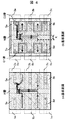
図1は本発明の第一実施例である電力変換装置を示す。本電力変換装置は、PWM整流器側の半導体スイッチングデバイス1a〜1c,インバータ側の半導体スイッチングデバイス2a〜2c,プリント基板3,コンデンサ4a〜4h,抵抗5a〜5dにより構成されている。プリント基板3は、PWM整流器の直流側とインバータの直流側を接続して直流リンク部を形成しており、直流リンク部の正極と負極の間に、複数のコンデンサ4a〜4hから成る平滑コンデンサが接続される。半導体スイッチングデバイス1a〜1cおよび2a〜2cは直列接続された2個のスイッチ素子(トランジスタ,IGBTなど)が搭載されたデバイスであり、第一のスイッチ素子のコレクタ部分が正極側端子C(+)として、第二のスイッチ素子のエミッタ部分が負極側端子E(−)として、第一および第二のスイッチ素子を直列接続する接点である第一のスイッチ素子のエミッタ部分と第二のスイッチ素子のコレクタ部分が交流端子として、それぞれ外部に接続される。
FIG. 1 shows a power conversion apparatus according to a first embodiment of the present invention. This power conversion device is composed of
図2は、図1下部の矢印方向から見た矢視図である。PWM整流器側およびインバータ側の半導体スイッチングデバイスの上部にプリント基板3を配置しており、プリント基板3上にコンデンサおよび抵抗を実装している。
FIG. 2 is an arrow view seen from the arrow direction at the bottom of FIG. A printed
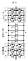
図3は、第一実施例の回路図である。本回路において、PWM整流器は電源の商用交流電力を直流に変換し、インバータは直流を任意周波数の交流に逆変換する。図1のプリント基板3は、PWM整流器およびインバータの正極端子(+極端子)どうしと負極端子(−極端子)どうしを接続しており、図3のように正極端子と負極端子の間にコンデンサおよび抵抗を接続している。また、図1のプリント基板3に搭載されたコンデンサは耐圧を満足するために図3のように2直列4並列の構成にしている。すなわち、図1のコンデンサ4aとコンデンサ4b,コンデンサ4cとコンデンサ4d,コンデンサ4eとコンデンサ4f,コンデンサ4gとコンデンサ4hがそれぞれ直列接続される。さらに、コンデンサ4a,コンデンサ4c,コンデンサ4e,コンデンサ4gの各正極端子がPWM整流器およびインバータの正極に接続され、コンデンサ4b,コンデンサ4d,コンデンサ4f,コンデンサ4hの各負極端子がPWM整流器およびインバータの負極に接続される。また、抵抗5a〜5dは直列接続されたコンデンサの電圧バランスを補償するためのバランス抵抗であり、図3のように、抵抗5aと抵抗5b、および、抵抗5cと抵抗5dを直列接続し、その中点を、直列接続したコンデンサの中点に接続する。
FIG. 3 is a circuit diagram of the first embodiment. In this circuit, the PWM rectifier converts the commercial AC power of the power source into direct current, and the inverter reversely converts the direct current into alternating current of an arbitrary frequency. The printed
図1の第一実施例において、PWM整流器を構成する各半導体スイッチングデバイスは、正極端子および負極端子の並ぶ方向および並ぶ順序が同一になるように配置される。また、インバータを構成する各半導体スイッチングデバイスも同様に配置される。PWM整流器側半導体スイッチングデバイス1a〜1c近傍のコンデンサ4e〜4hの正極端子および負極端子が並ぶ方向は半導体スイッチングデバイス1a〜1cと略同じであるが、並ぶ順序は相反する。同様に、インバータ側半導体スイッチングデバイス2a〜2c近傍のコンデンサ4a〜4dの正極端子および負極端子が並ぶ方向は半導体スイッチングデバイス2a〜2cと略同じであるが、並ぶ順序は相反する。このような配置によれば、任意の1つの半導体スイッチングデバイス(例えば2a)の正極端子と、その半導体スイッチングデバイスの近傍に位置する直列コンデンサの組(例えば、4aと4b)の正極端子とを結ぶプリント基板上の電流経路と、同じ半導体スイッチングデバイスの負極端子と、同じ直列コンデンサの組の負極端子とを結ぶプリント基板上の電流経路とが交差する。
In the first embodiment of FIG. 1, the semiconductor switching devices constituting the PWM rectifier are arranged so that the arrangement direction and the arrangement order of the positive terminal and the negative terminal are the same. Moreover, each semiconductor switching device which comprises an inverter is arrange | positioned similarly. The direction in which the positive and negative terminals of the
この場合は、例えば、インバータ側の半導体スイッチングデバイス2aがスイッチングすると、近傍の直列コンデンサ4a,4bの正極端子に流れる電流の経路と負極端子に流れる電流の経路が、図1のプリント基板3上に示す実線矢印のように互いに交わるので、電流により発生する磁束は強めあう方向になるためインピーダンスが増加する。一方、離れた位置の直列コンデンサ4e,4fでは、図1のプリント基板3上に示す点線矢印のように互いに正極端子に流れる電流と負極端子に流れる電流が相反する向きに流れるため、発生する磁束は相殺されインピーダンスは低下する。すなわち、半導体スイッチングデバイス2aと近傍のコンデンサとの間のインピーダンスと、半導体スイッチングデバイス2aと離れたコンデンサとの間のインピーダンスの違いが低減される。この結果、コンデンサに流れる電流のばらつきを低減できる。
In this case, for example, when the
なお、図1の実施例では、各半導体スイッチングデバイスにおいて、正極端子C(+),C(−)および交流端子が、この順序で直線的に配置される。さらに、プリント基板3の縦方向に対して半導体スイッチングデバイスとコンデンサを線対称に配置している。これにより、PWM整流器およびインバータの各相の交流端子がプリント基板3の外側に配置され、外部接続が容易にできる。
In the embodiment of FIG. 1, in each semiconductor switching device, the positive terminals C (+), C (−) and the AC terminal are linearly arranged in this order. Further, the semiconductor switching device and the capacitor are arranged symmetrically with respect to the vertical direction of the printed
図4は第一実施例のプリント基板3のパターンの一例を示す。プリント基板3は両面導体基板であり、表面に正極側の層(P層)を裏面に中点の層(C1層,C2層)および負極側の層(N層)を有している。インバータ側の半導体スイッチングデバイス2aがスイッチングした場合の電流経路としては、半導体スイッチングデバイス2aから離れた位置のコンデンサではプリント基板の表裏で相反する方向に電流が流れるが、近傍のコンデンサ(例えばコンデンサ4a,4b)では、磁束が強め合う経路を避けるために電流は迂回して流れることになる。この結果、電流経路のインピーダンスのばらつきが小さくなり、コンデンサに流れる電流のばらつきが低減される。
FIG. 4 shows an example of the pattern of the printed
なお、図1に示すように、PWM整流器側の直列コンデンサ(4eと4f,4gと4h)の一方の端子である各負極端子と、インバータ側の直列コンデンサ(4aと4b,4cと4d)の一方の端子である各負極端子が、プリント基板3の中央部において対向している。すなわち、これら負極端子がプリント基板中央部に集まっている。これにより、図4に示すような表裏両面に導体層を有する比較的簡単な構成の1枚の導体基板で、PWM整流器側とインバータ側両方における多数のコンデンサを接続して、平滑コンデンサを構成することができる。
In addition, as shown in FIG. 1, each negative terminal which is one terminal of the series capacitors (4e and 4f, 4g and 4h) on the PWM rectifier side, and the series capacitors (4a and 4b, 4c and 4d) on the inverter side Each negative terminal which is one terminal is opposed to the central portion of the printed
図5は、本発明者が行った、第一実施例におけるコンデンサの電流分布のシミュレーションの結果を示す。インバータ側の半導体スイッチングデバイス2aをスイッチングし、立ち上がり時間を有する振幅1(pu)のステップ電流を流した場合である。図5より、コンデンサ4eにおいて立ち上がり時に最大の電流が流れ、平均0.25(pu)に対して0.28(pu)となる。これは、図10の従来の場合の0.31(pu)よりも低減されている。さらに、最小電流も平均値に近づいており電流のばらつきが低減できている。
FIG. 5 shows the result of the simulation of the current distribution of the capacitor in the first embodiment performed by the present inventors. This is a case where the
また、図4の基板構成において、図4(b)の基板裏面の負極側の層(N層)における縦方向の電流経路部分の幅Xが広い方が、電流の相殺効果が大きくインピーダンスを低下できる。この場合、スイッチングする半導体スイッチングデバイスから離れたコンデンサの電流に対するばらつきの低減効果が大きくなる。実装構成としては、インバータ側のコンデンサ4a〜4dとPWM整流器側のコンデンサ4e〜4hの距離を広げる、つまり、直列接続したコンデンサ4aとコンデンサ4bの距離よりもインバータ側のコンデンサ4bとPWM整流器側のコンデンサ4eの距離が大きくなるようにコンデンサを配置する。
Further, in the substrate configuration of FIG. 4, when the width X of the current path portion in the vertical direction in the negative electrode layer (N layer) on the back surface of the substrate in FIG. it can. In this case, the effect of reducing variation with respect to the current of the capacitor away from the semiconductor switching device to be switched increases. As a mounting configuration, the distance between the
さらに、図1の第一実施例では、図3の回路図および図4の基板構成のように、PWM整流器側の中点の層(C1層)とインバータ側の中点の層(C2層)を電気的に分離しており、PWM整流器側とインバータ側のそれぞれに電圧バランス用の抵抗を接続している。これにより、コンデンサと抵抗間のインピーダンスが均等化され、かつ、C1層とC2層の間に不要な循環電流が流れることを防止できる。従って、安定したバランス効果を得られる。 Further, in the first embodiment of FIG. 1, as shown in the circuit diagram of FIG. 3 and the substrate configuration of FIG. 4, the midpoint layer (C1 layer) on the PWM rectifier side and the midpoint layer (C2 layer) on the inverter side Are electrically separated, and a voltage balancing resistor is connected to each of the PWM rectifier side and the inverter side. Thereby, the impedance between the capacitor and the resistor is equalized, and unnecessary circulating current can be prevented from flowing between the C1 layer and the C2 layer. Therefore, a stable balance effect can be obtained.
図6は、本発明の第二実施例である電力変換装置を示す。本実施例では、第一実施例よりもコンデンサの並列数を増やしている。図6では2直列8並列の構成であり、コンデンサ4aとコンデンサ4b,コンデンサ4cとコンデンサ4d,コンデンサ4eとコンデンサ4f,コンデンサ4gとコンデンサ4h,コンデンサ4iとコンデンサ4j,コンデンサ4kとコンデンサ4l,コンデンサ4mとコンデンサ4n,コンデンサ4oとコンデンサ4pがそれぞれ直列接続される。さらに、コンデンサ4a,コンデンサ4c,コンデンサ4e,コンデンサ4g,コンデンサ4j,コンデンサ4l,コンデンサ4n,コンデンサ4pの各正極端子がPWM整流器およびインバータの正極に接続され、コンデンサ4b,コンデンサ4d,コンデンサ4f,コンデンサ4h,コンデンサ4i,コンデンサ4k,コンデンサ4m,コンデンサ4oの各負極端子がPWM整流器およびインバータの負極に接続される。
FIG. 6 shows a power conversion apparatus according to the second embodiment of the present invention. In this embodiment, the number of capacitors in parallel is increased as compared with the first embodiment. In FIG. 6, two series and eight parallel configurations are used, and
本実施例においても、図1の第一実施例と同様に、PWM整流器側およびインバータ側の各々において、半導体スイッチングデバイスの正および負極端子とコンデンサの正および負極端子の並ぶ方向が略同じになり、かつ、並ぶ順序が相反するように、半導体スイッチングデバイスとコンデンサが配置される。これにより、コンデンサに流れる電流のばらつきを低減できる。このばらつき低減効果は、コンデンサの並列段数が多くなり半導体スイッチングデバイスと、これから最も離れたコンデンサとの距離が長くなるほど顕著に現れ、コンデンサの負担を分散できる。従って、コンデンサが長寿命化できる。 Also in this embodiment, as in the first embodiment of FIG. 1, the alignment direction of the positive and negative terminals of the semiconductor switching device and the positive and negative terminals of the capacitor is substantially the same on each of the PWM rectifier side and the inverter side. In addition, the semiconductor switching device and the capacitor are arranged so that the order of arrangement is opposite. Thereby, the dispersion | variation in the electric current which flows into a capacitor | condenser can be reduced. This variation reducing effect becomes more prominent as the number of parallel stages of capacitors increases and the distance between the semiconductor switching device and the capacitor farthest from this increases, and the burden on the capacitor can be dispersed. Therefore, the life of the capacitor can be extended.
図7は、本発明の第三実施例である電力変換装置を示す。また、本実施例の回路図を図8に示す。本実施例では、電圧耐量の大きいコンデンサ6a〜6dを使用しているので、直流リンク部の正極(P)と負極(N)の間には、各コンデンサが単独で接続される。すなわち、複数のコンデンサを直列接続することなく、単独のコンデンサが4個並列に接続され、平滑コンデンサが構成されている。このため、バランス用の抵抗は接続しない。本実施例においても、第一および第二実施例と同様に、本実施例においても、図1の第一実施例と同様に、PWM整流器側およびインバータ側の各々において、半導体スイッチングデバイスの正および負極端子とコンデンサの正および負極端子の並ぶ方向が同じになり、かつ、並ぶ順序が相反するように、半導体スイッチングデバイスとコンデンサが配置される。これにより、コンデンサに流れる電流のばらつきを低減できる。
FIG. 7 shows a power conversion apparatus according to the third embodiment of the present invention. A circuit diagram of this embodiment is shown in FIG. In the present embodiment, the
第一および第二実施例では、PWM整流器側とインバータ側の半導体スイッチングデバイスおよびコンデンサを共にプリント基板で接続しているが、別の導体基板を使用し、コンデンサが接続されたプリント基板と並列に、PWM整流器側半導体スイッチングデバイスとインバータ側半導体スイッチングデバイスのそれぞれの正極端子同士および負極端子同士を接続しても良い。この場合は、プリント基板には高周波のリプル成分が主に流れ、主電流成分が別の導体基板を流れるので、プリント基板の発熱を抑制できる。 In the first and second embodiments, the PWM rectifier side and inverter side semiconductor switching devices and capacitors are both connected by a printed circuit board, but a different conductor board is used in parallel with the printed circuit board to which the capacitor is connected. The positive terminals and the negative terminals of the PWM rectifier side semiconductor switching device and the inverter side semiconductor switching device may be connected to each other. In this case, since the high frequency ripple component mainly flows through the printed circuit board and the main current component flows through another conductor substrate, heat generation of the printed circuit board can be suppressed.
以上、本発明の実施の形態を説明したが、本発明は上記の実施形態に限定されるものではなく、その技術的思想の範囲内で様々な形態が可能である。 Although the embodiment of the present invention has been described above, the present invention is not limited to the above-described embodiment, and various forms are possible within the scope of the technical idea.
1a〜1c PWM整流器側の半導体スイッチングデバイス
2a〜2c インバータ側の半導体スイッチングデバイス
3 プリント基板
4a〜4p,6a〜6c コンデンサ
5a〜5d 抵抗
1a to 1c PWM rectifier side
Claims (4)
前記複数の半導体スイッチングデバイスの上部に配置されるプリント基板に搭載され、前記複数の半導体スイッチングデバイスの正極端子と負極端子の間に接続される複数のコンデンサと、
を備える電力変換装置において、
前記半導体スイッチングデバイスの各々における正極端子及び負極端子の並ぶ方向と、前記複数のコンデンサの内、前記各半導体スイッチングデバイスの近傍に位置するコンデンサの正極端子及び負極端子の並ぶ方向は略同じであり、かつ、前記各半導体スイッチングデバイスの正極端子及び負極端子の並ぶ順序と、前記各半導体スイッチングデバイスの近傍に位置する前記コンデンサの正極端子及び負極端子の並ぶ順序は相反し、
前記複数の半導体スイッチングデバイスおよび前記複数のコンデンサは、前記各正極端子及び前記各負極端子の位置関係が線対称になるように配置され、
前記複数のコンデンサの各々は2直列以上に直列接続した構成であり、前記線対称配置の一方側におけるコンデンサにおいて直列接続の中点同士を短絡し、かつ、前記線対称配置の他方側におけるコンデンサにおいて直列接続の中点同士を短絡し、
前記一方側に配置される直列接続のコンデンサ間の距離あるいは前記他方側に配置される直列接続のコンデンサ間の距離よりも、前記一方側に配置される直列接続のコンデンサと前記他方側に配置されるコンデンサとの最短距離の方が大きいことを特徴とする電力変換装置。 A plurality of semiconductor switching devices ;
A plurality of capacitors mounted on a printed circuit board disposed on top of the plurality of semiconductor switching devices , and connected between positive and negative terminals of the plurality of semiconductor switching devices ;
In a power converter comprising:
Wherein the positive terminal and the direction of arrangement of the negative electrode terminal of each of the semiconductor switching devices, the plurality of capacitors, the positive electrode terminal and the direction of arrangement of the negative terminal of the capacitor to be located in the vicinity of each of the semiconductor switching devices are substantially the same, And the order in which the positive electrode terminal and the negative electrode terminal of each semiconductor switching device are arranged and the order in which the positive electrode terminal and the negative electrode terminal of the capacitor located in the vicinity of each semiconductor switching device are contradictory ,
The plurality of semiconductor switching devices and the plurality of capacitors are arranged so that the positional relationship between each positive terminal and each negative terminal is axisymmetric,
Each of the plurality of capacitors has a configuration in which two or more series are connected in series, and short-circuits the middle points of the series connection in the capacitor on one side of the line-symmetric arrangement, and in the capacitor on the other side of the line-symmetric arrangement Short-circuit the midpoints of the series connection,
More than the distance between the series-connected capacitors arranged on the one side or the distance between the series-connected capacitors arranged on the other side, it is arranged on the other side with the series-connected capacitors arranged on the one side. A power converter characterized in that the shortest distance to the capacitor is larger .
Priority Applications (3)
| Application Number | Priority Date | Filing Date | Title |
|---|---|---|---|
| JP2008057155A JP4597202B2 (en) | 2008-03-07 | 2008-03-07 | Power converter |
| CN 200810211076 CN101527523B (en) | 2008-03-07 | 2008-08-20 | Power converter |
| EP09001957A EP2099117A3 (en) | 2008-03-07 | 2009-02-12 | Electric power converter |
Applications Claiming Priority (1)
| Application Number | Priority Date | Filing Date | Title |
|---|---|---|---|
| JP2008057155A JP4597202B2 (en) | 2008-03-07 | 2008-03-07 | Power converter |
Publications (2)
| Publication Number | Publication Date |
|---|---|
| JP2009219175A JP2009219175A (en) | 2009-09-24 |
| JP4597202B2 true JP4597202B2 (en) | 2010-12-15 |
Family
ID=40732231
Family Applications (1)
| Application Number | Title | Priority Date | Filing Date |
|---|---|---|---|
| JP2008057155A Active JP4597202B2 (en) | 2008-03-07 | 2008-03-07 | Power converter |
Country Status (3)
| Country | Link |
|---|---|
| EP (1) | EP2099117A3 (en) |
| JP (1) | JP4597202B2 (en) |
| CN (1) | CN101527523B (en) |
Families Citing this family (15)
| Publication number | Priority date | Publication date | Assignee | Title |
|---|---|---|---|---|
| CN102347697B (en) * | 2010-07-29 | 2014-01-01 | 上海儒竞电子科技有限公司 | Direct DC-AC (direct current-alternating current) converting circuit for low-voltage input full bridge inverter |
| CN102215007B (en) * | 2011-05-27 | 2013-11-20 | 唐险峰 | Power control circuit board |
| JP5686677B2 (en) * | 2011-06-13 | 2015-03-18 | 住友重機械工業株式会社 | Power converter |
| EP2584686A1 (en) * | 2011-10-20 | 2013-04-24 | Siemens Aktiengesellschaft | Balancing circuit for series connected dc-link capacitors and method for its operation |
| EP2584685A1 (en) * | 2011-10-20 | 2013-04-24 | Siemens Aktiengesellschaft | Balancing circuit for series connected dc-link capacitors and method for its operation |
| US9178410B2 (en) * | 2012-01-06 | 2015-11-03 | General Electric Company | Adaptive power conversion system |
| JP5957303B2 (en) * | 2012-06-08 | 2016-07-27 | 日立アプライアンス株式会社 | Power conversion device and distributed power supply system |
| WO2014033857A1 (en) * | 2012-08-29 | 2014-03-06 | 株式会社安川電機 | Power conversion apparatus |
| JP2014110721A (en) * | 2012-12-04 | 2014-06-12 | Samsung Electronics Co Ltd | Power conversion device |
| CN107534391B (en) * | 2015-04-20 | 2019-12-03 | 三菱电机株式会社 | Power conversion device |
| KR20170111592A (en) * | 2016-03-29 | 2017-10-12 | 엘에스산전 주식회사 | Apparatus for voltage balancing for dc link capacitor in inverter |
| DE112017007484T5 (en) * | 2017-04-27 | 2020-01-09 | Mitsubishi Electric Corporation | Power conversion unit |
| DE102017110608A1 (en) * | 2017-05-16 | 2018-11-22 | Valeo Siemens Eautomotive Germany Gmbh | inverter |
| JP6317516B1 (en) * | 2017-11-01 | 2018-04-25 | 高周波熱錬株式会社 | DC smoothing circuit, inverter, and power supply device |
| CN109861577B (en) * | 2019-03-28 | 2021-02-02 | 孙驰 | Power conversion circuit |
Citations (2)
| Publication number | Priority date | Publication date | Assignee | Title |
|---|---|---|---|---|
| JPH02294278A (en) * | 1989-04-28 | 1990-12-05 | Mitsubishi Electric Corp | Inverter device |
| JP2002051569A (en) * | 2000-08-03 | 2002-02-15 | Toshiba Corp | Power converter |
Family Cites Families (7)
| Publication number | Priority date | Publication date | Assignee | Title |
|---|---|---|---|---|
| JP3424532B2 (en) * | 1997-11-25 | 2003-07-07 | 株式会社日立製作所 | Power converter |
| JP3046276B2 (en) * | 1998-05-11 | 2000-05-29 | 三菱電機株式会社 | Power converter |
| JP3501685B2 (en) * | 1999-06-04 | 2004-03-02 | 三菱電機株式会社 | Power converter |
| JP3906440B2 (en) * | 2000-09-06 | 2007-04-18 | 株式会社日立製作所 | Semiconductor power converter |
| JP2003219661A (en) * | 2002-01-24 | 2003-07-31 | Toshiba Mach Co Ltd | Servo amplifier |
| US7248483B2 (en) * | 2004-08-19 | 2007-07-24 | Xantrex Technology, Inc. | High power density insulated metal substrate based power converter assembly with very low BUS impedance |
| JP2006197735A (en) | 2005-01-14 | 2006-07-27 | Meidensha Corp | Inverter |
-
2008
- 2008-03-07 JP JP2008057155A patent/JP4597202B2/en active Active
- 2008-08-20 CN CN 200810211076 patent/CN101527523B/en active Active
-
2009
- 2009-02-12 EP EP09001957A patent/EP2099117A3/en not_active Withdrawn
Patent Citations (2)
| Publication number | Priority date | Publication date | Assignee | Title |
|---|---|---|---|---|
| JPH02294278A (en) * | 1989-04-28 | 1990-12-05 | Mitsubishi Electric Corp | Inverter device |
| JP2002051569A (en) * | 2000-08-03 | 2002-02-15 | Toshiba Corp | Power converter |
Also Published As
| Publication number | Publication date |
|---|---|
| CN101527523A (en) | 2009-09-09 |
| CN101527523B (en) | 2013-05-15 |
| JP2009219175A (en) | 2009-09-24 |
| EP2099117A2 (en) | 2009-09-09 |
| EP2099117A3 (en) | 2011-03-16 |
Similar Documents
| Publication | Publication Date | Title |
|---|---|---|
| JP4597202B2 (en) | Power converter | |
| US9538680B2 (en) | Laminated busbar for power converter and the converter thereof | |
| US9570972B2 (en) | CR snubber circuit | |
| JP4973697B2 (en) | Power converter | |
| EP3203625B1 (en) | Electric power conversion apparatus | |
| JP4929299B2 (en) | Power converter | |
| JP5807516B2 (en) | Power converter and method of arranging conductor in power converter | |
| US9320134B2 (en) | DC-DC converter module and multi-layer substrate | |
| US11424690B2 (en) | Semiconductor switching arrangement | |
| JP6184507B2 (en) | Driver board and power conversion device | |
| JP2008271696A (en) | Power conversion apparatus | |
| JP2009261106A (en) | Electrical circuit | |
| JP6035766B2 (en) | LED lighting device | |
| US10284111B2 (en) | Power conversion apparatus having connection conductors having inductance which inhibits ripple current | |
| JP2005176555A (en) | Power converter | |
| JPH073851B2 (en) | Parallel connection of power transistors | |
| CN116470357A (en) | PCB busbar and motor controller | |
| JP2014110721A (en) | Power conversion device | |
| JP6720601B2 (en) | Power converter | |
| JP6314099B2 (en) | Power converter | |
| JP6851242B2 (en) | Power converter | |
| JP7028359B1 (en) | Power converter | |
| JP4765662B2 (en) | Inverter device | |
| JP2007006571A (en) | Power converter | |
| JP5840527B2 (en) | Circuit board |
Legal Events
| Date | Code | Title | Description |
|---|---|---|---|
| A621 | Written request for application examination |
Free format text: JAPANESE INTERMEDIATE CODE: A621 Effective date: 20100201 |
|
| A977 | Report on retrieval |
Free format text: JAPANESE INTERMEDIATE CODE: A971007 Effective date: 20100517 |
|
| A131 | Notification of reasons for refusal |
Free format text: JAPANESE INTERMEDIATE CODE: A131 Effective date: 20100615 |
|
| A521 | Written amendment |
Free format text: JAPANESE INTERMEDIATE CODE: A523 Effective date: 20100810 |
|
| TRDD | Decision of grant or rejection written | ||
| A01 | Written decision to grant a patent or to grant a registration (utility model) |
Free format text: JAPANESE INTERMEDIATE CODE: A01 Effective date: 20100907 |
|
| A01 | Written decision to grant a patent or to grant a registration (utility model) |
Free format text: JAPANESE INTERMEDIATE CODE: A01 |
|
| A61 | First payment of annual fees (during grant procedure) |
Free format text: JAPANESE INTERMEDIATE CODE: A61 Effective date: 20100921 |
|
| R151 | Written notification of patent or utility model registration |
Ref document number: 4597202 Country of ref document: JP Free format text: JAPANESE INTERMEDIATE CODE: R151 |
|
| FPAY | Renewal fee payment (event date is renewal date of database) |
Free format text: PAYMENT UNTIL: 20131001 Year of fee payment: 3 |