JP4579306B2 - Circular plating tank - Google Patents
Circular plating tank Download PDFInfo
- Publication number
- JP4579306B2 JP4579306B2 JP2008050813A JP2008050813A JP4579306B2 JP 4579306 B2 JP4579306 B2 JP 4579306B2 JP 2008050813 A JP2008050813 A JP 2008050813A JP 2008050813 A JP2008050813 A JP 2008050813A JP 4579306 B2 JP4579306 B2 JP 4579306B2
- Authority
- JP
- Japan
- Prior art keywords
- plating
- substrate
- plating tank
- circular
- tank
- Prior art date
- Legal status (The legal status is an assumption and is not a legal conclusion. Google has not performed a legal analysis and makes no representation as to the accuracy of the status listed.)
- Expired - Fee Related
Links
Images


Classifications
-
- C—CHEMISTRY; METALLURGY
- C25—ELECTROLYTIC OR ELECTROPHORETIC PROCESSES; APPARATUS THEREFOR
- C25D—PROCESSES FOR THE ELECTROLYTIC OR ELECTROPHORETIC PRODUCTION OF COATINGS; ELECTROFORMING; APPARATUS THEREFOR
- C25D17/00—Constructional parts, or assemblies thereof, of cells for electrolytic coating
- C25D17/02—Tanks; Installations therefor
-
- C—CHEMISTRY; METALLURGY
- C25—ELECTROLYTIC OR ELECTROPHORETIC PROCESSES; APPARATUS THEREFOR
- C25D—PROCESSES FOR THE ELECTROLYTIC OR ELECTROPHORETIC PRODUCTION OF COATINGS; ELECTROFORMING; APPARATUS THEREFOR
- C25D17/00—Constructional parts, or assemblies thereof, of cells for electrolytic coating
- C25D17/06—Suspending or supporting devices for articles to be coated
Landscapes
- Chemical & Material Sciences (AREA)
- Engineering & Computer Science (AREA)
- Chemical Kinetics & Catalysis (AREA)
- Electrochemistry (AREA)
- Materials Engineering (AREA)
- Metallurgy (AREA)
- Organic Chemistry (AREA)
- Electroplating Methods And Accessories (AREA)
Description
本発明は、めっき槽に関し、より詳しくは、めっき対象の基板の表面に微細パターンを形成するための薄く均一なめっき層を形成するためのめっき槽に関する。 The present invention relates to a plating tank, and more particularly to a plating tank for forming a thin and uniform plating layer for forming a fine pattern on the surface of a substrate to be plated.
一般に、めっきとは、めっきを施す金属を陰極とし、電着させる金属を陽極として、電着させる金属のイオンを含有した電解液中に入れ、電気を通すことによって金属イオンがめっきを施す金属の表面に析出されるようにする方法をいう。 In general, plating is a method in which a metal to be plated is placed in an electrolytic solution containing ions of the metal to be electrodeposited by using the metal to be plated as a cathode and the metal to be electrodeposited as an anode, and by conducting electricity. A method of depositing on the surface.
このようなめっき法で形成するめっき層は、必要な範囲内で薄いほど有利であり、全面に亘る均一性を確保しながら薄いめっき層を形成することが重要な課題となってきている。 A plating layer formed by such a plating method is more advantageous as it is thinner within a necessary range, and it is an important issue to form a thin plating layer while ensuring uniformity over the entire surface.
特に、半導体工程で用いられる基板は、主に電解めっき装置によって表面処理されており、電解めっきによって、銅や金などの金属を被覆して、主に、回路パターンとバンプなどが形成される。 In particular, a substrate used in a semiconductor process is mainly surface-treated by an electroplating apparatus, and a metal such as copper or gold is coated by electroplating to mainly form circuit patterns and bumps.
また、半導体工程をはじめとする電子材料として用いられる基板は、他のめっき処理より要求される特性に制限が多く、めっき厚さの均一性、めっき面の平滑性およびめっきの付着性などが主要なめっき品質基準となり、特にめっき厚さにおいては、被めっき面の全体に後の工程に有利なように均一なめっき層が形成されるようにすることが厳格に要求されている。 Also, substrates used as electronic materials such as semiconductor processes are more limited in the characteristics required than other plating processes, and the main features are uniformity of plating thickness, smoothness of plating surface, and adhesion of plating. In particular, with respect to the plating thickness, it is strictly required that a uniform plating layer be formed on the entire surface to be plated so as to be advantageous for subsequent processes.
したがって、めっき厚さの均一性を向上させるために、めっき槽内においてめっき電流の電流分布を均一に維持するようにしなければならない。 Therefore, in order to improve the uniformity of the plating thickness, the current distribution of the plating current must be maintained uniformly in the plating tank.
しかし、従来のめっき槽は主に四角の箱状に構成され、その内部に複数の基板が並列に配置されることによって、めっき電流の分布に代表されるめっき層を形成するためのイオンの分布を均一にして薄い均一なめっき層を得ることが難しいという問題点がある。 However, the conventional plating tank is mainly configured in a square box shape, and the distribution of ions to form a plating layer represented by the distribution of plating current by arranging a plurality of substrates in parallel inside There is a problem that it is difficult to obtain a uniform thin plating layer with uniform thickness.
特に、現在の多様な形態の電子装置材料として用いられる基板の場合には、微細パターンを印刷しなければならないため、基板の表面に非常に薄いめっき層が形成されるようにしなければならないが、従来のめっき槽では微細パターン印刷が可能な約30μm以下の厚さのめっき層の形成は技術的に難しい。 In particular, in the case of a substrate used as an electronic device material in various forms, since a fine pattern must be printed, a very thin plating layer must be formed on the surface of the substrate. In a conventional plating tank, it is technically difficult to form a plating layer having a thickness of about 30 μm or less capable of fine pattern printing.
次に、従来のめっき槽の構造と従来のめっき槽を用いためっき法について簡略的に見ると次の通りである。 Next, the structure of the conventional plating tank and the plating method using the conventional plating tank will be briefly described as follows.
図1は、従来のめっき槽の構成図であって、図に示すように従来のめっき槽は四角のめっき槽1内にめっき液2が充填され、充填されためっき液中に複数の基板3が並列に配列される。
FIG. 1 is a configuration diagram of a conventional plating tank. As shown in the figure, a conventional plating tank is filled with a
めっき槽1は、上部が開放された四角箱状に構成され、陽電荷端子による陽電流が通電する溶液が収容されためっき槽として構成されている。 The plating tank 1 is configured as a square box having an open top, and is configured as a plating tank that contains a solution that is energized by a positive current from a positive charge terminal.
また、めっき槽1の上部に陰電荷端子と接続され、陰電流が通電し、表面にめっき層が形成される基板3が結合された搬送手段(図示せず)が備えられる。
Further, a conveying means (not shown) is provided on the upper part of the plating tank 1 and connected to a negative charge terminal, to which a negative current is passed, and a
従来のめっき槽1では、搬送手段にめっきを施す基板を懸垂方式で固定し、めっき槽1内のめっき液内に浸し搬送手段によって、往復させることにより、めっき槽1内で電流通電による化学反応によって、基板3の表面に薄い皮膜としてめっき層が形成される。
In the conventional plating tank 1, the substrate to be plated is fixed to the conveying means by a suspension method, immersed in the plating solution in the plating tank 1, and reciprocated by the conveying means, thereby causing a chemical reaction by current conduction in the plating tank 1. Thus, a plating layer is formed as a thin film on the surface of the
しかし、従来のめっき槽1は、めっきを行う過程で、主に基板2が薄板状に構成されていることによって、基板2が搬送手段に固定され、めっき液中で搬送される過程でめっき液の抵抗力によって、搬送手段に直接固定されていない部分で流動が発生する場合がある。
However, the conventional plating tank 1 is a process in which the
したがって、基板3の全面に亘って均一な厚さを有するめっき層を形成できないという問題点がある。
Therefore, there is a problem that a plating layer having a uniform thickness cannot be formed over the entire surface of the
また、図2は、従来のめっき槽1のめっき進行時のイオン分布を示す図であり、従来のめっき槽1において、内部に満たされためっき液中に基板3を並列に配列した後の時間経過に伴う基板3の周囲のイオン分布を示している。
FIG. 2 is a diagram showing the ion distribution during plating in the conventional plating tank 1, and the time after the
図2に示すように、めっき槽1内の流動がないめっき液内に基板3を並列に配列した時、基板3の周囲のイオンが析出され、基板3の表面に固定されることによってめっき液内では徐々にイオンの量が減少する。
As shown in FIG. 2, when the
したがって、時間が経過するほどめっき槽1内の最外郭に配置された基板3の周囲とその内側に配置された基板3の周囲に分布するイオンの分布が不均一になり、それによって、基板3の配列位置によっては表面全体に均一な厚さのめっき層が形成されにくくなるという問題が生じる。
Therefore, as time passes, the distribution of ions distributed around the
また、このような問題点を単純に改善するために、四角のめっき槽1内に収容されためっき液を強制的に循環させる方法が工夫されているが、前記問題点を解決する完全な解決策にはなり得ず、めっき液の揺れによって、先に説明したようにめっき層の厚さが不均一になる場合があるという問題がやはり発生し得る。 Further, in order to simply improve such problems, a method for forcibly circulating the plating solution accommodated in the square plating tank 1 has been devised, but a complete solution to solve the above problems As described above, there may be a problem that the thickness of the plating layer may be non-uniform due to the shaking of the plating solution.
このような問題点を解決するために、めっき槽1内に並列に配列された基板3の一面に補助陰極を密着させ、補助陰極と一定の間隔をおいて、遮蔽板を配置することによって、基板3の電界分布を拡大させ、基板3の表面に均一なめっき層が形成されるようにする方法が提案されている。
In order to solve such a problem, the auxiliary cathode is brought into close contact with one surface of the
しかし、遮蔽板を用いためっき法では、先に説明した問題点と短所を根本的に解消することが困難であり、めっき層を形成しなければならない基板3の縁にめっき電流が集中するのを遮蔽板によって防止できることはできるが、縁のめっき面積が大きい場合には、めっき偏差が発生せざるを得ないという問題点がある。
However, in the plating method using the shielding plate, it is difficult to fundamentally solve the problems and disadvantages described above, and the plating current is concentrated on the edge of the
したがって、本発明は、従来のめっき槽で発生する上記の短所と問題点を解決するために創案されたものであり、基板全面に均一なめっき層を形成することができるめっき槽を提供することを目的とする。 Accordingly, the present invention was devised to solve the above disadvantages and problems occurring in conventional plating tanks, and provides a plating tank capable of forming a uniform plating layer on the entire surface of the substrate. With the goal.
また、本発明は、円形のめっき槽内に分布したイオンがめっき槽の壁に沿って配置された各基板周囲に等しく分布することによって、基板位置に応じて発生する偏差を除去して微細パターン形成が可能な厚さの微細めっき層が形成されるようにした円形めっき槽を提供することに発明の目的がある。 In addition, the present invention eliminates the deviation generated according to the position of the substrate so that the ions distributed in the circular plating tank are equally distributed around each substrate arranged along the wall of the plating tank. It is an object of the invention to provide a circular plating tank in which a fine plating layer having a thickness that can be formed is formed.
前記の目的を達成するための本発明は、内部にめっき液が収容された円形のめっき槽と、めっき槽内に配置される基板を含む。 The present invention for achieving the above object includes a circular plating tank in which a plating solution is accommodated, and a substrate disposed in the plating tank.
めっき槽は、上部が開放された円形の水槽状に構成され、内部に基板を完全に浸すことができるようにめっき液が収容される。この時、めっき液としては、陽電流が通電されて内部のイオンが流動可能な溶液が収容される。 The plating tank is configured in a circular water tank shape with an open top, and contains a plating solution so that the substrate can be completely immersed therein. At this time, as the plating solution, a solution in which a positive current is passed and the internal ions can flow is accommodated.
また、めっき槽は、内部に環状の基板固定枠が装着され、基板固定枠には複数の基板を固定することのできる基板固定具が備えられる。 The plating tank has an annular substrate fixing frame mounted therein, and the substrate fixing frame is provided with a substrate fixing tool capable of fixing a plurality of substrates.
基板固定枠は、めっき槽の中央部に鉛直に配置された回転軸上に回転可能に結合し、基板固定枠に装着される基板は基板固定枠の形態に応じて多角形または円形状に配置される。 The substrate fixing frame is rotatably coupled on a rotating shaft vertically arranged at the center of the plating tank, and the substrate mounted on the substrate fixing frame is arranged in a polygon or a circle depending on the shape of the substrate fixing frame. Is done.
したがって、基板は、めっき液中に浸された状態で基板固定枠の回転方向に回転しながら、外部から加えられる熱源などのような外乱源に対して均一な影響を受けるようにし、めっき槽内における内部駆動によって、外乱の影響がめっき槽のめっき液内に均一に作用するようにできる。 Accordingly, the substrate is immersed in the plating solution while rotating in the direction of rotation of the substrate fixing frame, so that the substrate is uniformly affected by a disturbance source such as a heat source applied from the outside. Due to the internal driving, the influence of disturbance can be applied uniformly to the plating solution in the plating tank.
また、このようなめっき槽内の外乱の影響に対しては、めっき槽内でめっき液を循環させることによりその循環流動によって同様に均一化の効果を得ることができる。 Moreover, with respect to the influence of the disturbance in such a plating tank, the uniforming effect can be similarly obtained by circulating the plating solution in the plating tank.
一方、めっき槽内に配置された基板は、陰の電極と接続され、陰電位を有し、基板が浸されためっき液は、陽の電位を有する陽極と通電してめっき液内に電解されている電解質内の陽電荷を帯びたイオンが基板の表面に析出される。 On the other hand, the substrate disposed in the plating tank is connected to the negative electrode and has a negative potential, and the plating solution immersed in the substrate is electrolyzed in the plating solution by energizing the anode having a positive potential. The positively charged ions in the electrolyte are deposited on the surface of the substrate.
基板が陰電位を有する時、陽極はめっき槽の中心に配置するか、めっき槽内の基板の内側に円形状に配置することができる。 When the substrate has a negative potential, the anode can be placed in the center of the plating tank or in a circular shape inside the substrate in the plating tank.
また、電解めっきのための陽極は、基板の内壁面上に配置することもできる。 Moreover, the anode for electrolytic plating can also be arrange | positioned on the inner wall face of a board | substrate.
この時、陽極は複数を互いに一定の間隔を有するように配置してもよく、隙間がない円柱状に構成してもよい。 At this time, a plurality of anodes may be arranged so as to have a constant interval with each other, or may be configured in a columnar shape without a gap.
このような技術的構成を有する本発明の円形めっき槽は、円形のめっき槽内に基板を円形または円形に近い多角形を成すように配列して、基板をめっき液内で回転させることによって、外部から加えられる外乱に対する影響が一部の基板に集中するのを防止して、各基板に等しく分散させることによって、基板間でのめっきの偏差を減少させ、基板の全面に均一なめっき層が形成されるようにできることに技術的特徴がある。 In the circular plating tank of the present invention having such a technical configuration, by arranging the substrate in a circular plating tank so as to form a circle or a polygon close to a circle, and rotating the substrate in the plating solution, By preventing the influence on external disturbances from being concentrated on some substrates and distributing them equally to each substrate, the plating deviation between the substrates is reduced, and a uniform plating layer is formed on the entire surface of the substrate. There is a technical feature that can be formed.
本発明の円形めっき槽には、めっき液が収容される円形のめっき槽内に複数の基板を円形に近い多角形を成すように配置して、外乱発生時にその影響を均一化することによって基板全面に均一なめっき層を生成することができるという長所があり、基板位置によって発生する偏差を低減して、微細パターン形成が可能な厚さの0.5ないし30μmの微細めっき層を形成できるという利点がある。 In the circular plating tank of the present invention, a plurality of substrates are arranged so as to form a polygonal shape close to a circle in a circular plating tank in which a plating solution is accommodated, and the influence is made uniform when a disturbance occurs. There is an advantage that a uniform plating layer can be generated on the entire surface, and the deviation generated by the substrate position can be reduced, so that a fine plating layer having a thickness of 0.5 to 30 μm capable of forming a fine pattern can be formed. There are advantages.
本発明に係る円形めっき槽の上記の目的に対する技術的構成をはじめとする作用効果に関する事項は、本発明の好ましい実施形態が示された図面を参照した下記の詳細な説明によって明確に理解できるはずである。 Matters relating to the operational effects including the technical configuration for the above-described object of the circular plating tank according to the present invention should be clearly understood by the following detailed description with reference to the drawings showing preferred embodiments of the present invention. It is.
まず、図3は、本発明に係る円形めっき槽の斜視図であり、図4は、本発明に係る円形めっき槽の平面図である。 3 is a perspective view of a circular plating tank according to the present invention, and FIG. 4 is a plan view of the circular plating tank according to the present invention.
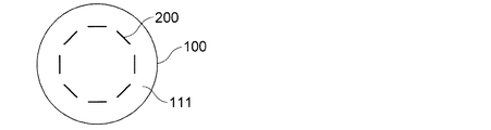
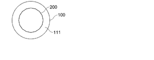
図に示すように、本実施形態の円形のめっき槽100は、その中央部に回転軸110が取り付けられ、めっき槽100内の回転軸110に基板固定枠120が装着され、基板固定枠120内にめっき対象の基板200が固定される。
As shown in the figure, the
めっき槽100は、上部が開放された円筒形に構成され、内部に陽極と、通電可能なイオン水溶液であるめっき液111が収容され、めっき槽100の一側部に、めっき槽100の内部にめっき液111を注入するためのめっき液注入口(図示せず)が備えられている。
The
この時、めっき槽100内に収容されためっき液111は、基板固定枠120に装着された基板200が十分に浸される高さまで満たされる。
At this time, the
回転軸110は、めっき槽100の中央部で回転できるように、めっき槽100の内部を貫通して取り付けられている。
The rotating
また、回転軸110に結合される基板固定枠120は環状に構成され、めっき槽100内の回転軸110の上下部に装着され、基板固定枠120の環状枠部には基板200の上下端部が結合される基板固定具121が備えられている。
Further, the
基板200は、上下端部が基板固定具121に個別的に結合されて、環状の基板固定枠120の枠部に沿って装着され、めっき液111内に浸された状態で回転軸110の回転によって、基板固定枠120の回転方向にめっき液111内で回転する。
The
一方、基板200は、めっき液111内に基板固定枠120に複数が鉛直に取り付け、基板固定枠120の枠部に沿って配置することによって、基板固定枠120の形状に応じて変化し得るが、全体として、図5のように円形または円形に近い多角形をなすように配置される。
On the other hand, a plurality of
図5a〜cは、本発明に係る円形めっき槽内の基板配列の例を示めす図であって、図に示すように基板200は、並列にではなく、円形または円形に近い多角形状に配置することが好ましい。
5a to 5c are diagrams showing examples of the substrate arrangement in the circular plating tank according to the present invention, and as shown in the figure, the
基板200の配列構造は、下記に説明する電極の配置構造と基板200の回転構造に応じて適宜変更可能であり、多様なシミュレーションを経て電極の配置などの多様な条件を考慮して、最も適する形態の配列にすることが好ましい。
The arrangement structure of the
このような技術的構成の円形のめっき槽100は、円形のめっき槽100の内部に基板固定枠120を用いて基板200を円形または円形に近い形態に配列し、内部の任意地点にアノード(anode)電極が備わっためっき槽100内にめっき液111を供給して、基板200とめっき液111を接触させると同時に基板200にめっき電流を供給すると、基板200の表面にめっき液111内のイオンが析出され、めっきが施される。
In the
また、基板200は、めっき槽100の形状に沿ってその内部に円形に配置されるが、場合によって、1列または2列以上の複数列に配列することもできる。
Moreover, although the board |
このように、円形めっき槽100内に基板200を円形または円形に近い多角形状に配置する理由は、電磁場や熱源およびめっき液の循環による流速変化などによる基板200の外部の影響、すなわち基板200のめっき層形成に不要な外乱がめっき槽100内の一側で発生した時、円形に近く配置された基板200を回転させることによって、基板200に加えられる外乱の影響を均一化するためである。
As described above, the reason why the
一方、本発明のめっき槽100は、回転軸110や基板200またはめっき槽100自体を回転させ、めっき槽100内のめっき液111を循環させ、めっき槽100内に個別に配置された基板200の表面に均一にめっきが施されるようにしている。
On the other hand, the
図6a,bは、本発明に係る円形めっき槽のめっき液循環構造を示す構成図であって、図に示すように本発明では、円形のめっき槽100はその内壁面から所定の間隔をおいた円形に近い形状をなすように基板200が配置され、めっき槽100内に、基板200を浸すことができるように収容されためっき液111が循環するようにしている。
6A and 6B are configuration diagrams showing a plating solution circulation structure of a circular plating tank according to the present invention. As shown in the figure, in the present invention, the
めっき液111を循環させるのは、めっき液111中に含まれたイオンが均等に分散して、めっき対象の基板200に均一に析出されるようにするためで、先に説明したように外乱発生時の外乱に対する影響が各基板200に等しく及ぶようにして、基板200の表面に均一なめっき層が形成されるようにするためでもある。
The
このような理由によって、めっき液111は、めっき槽100の中央部に取り付けられた回転軸110または回転軸110の結合位置に図6aのように別の回転部材300を装着し、この回転部材300の回転によってめっき液111を循環させるようにしている。
For this reason, the
また、図6bのようにめっき槽100の内部に装着された基板200の内側に円筒形のシリンダ310を設け、シリンダ310の回転によって、その内外のめっき液111がめっき槽100内で回転するようにすることもできる。
In addition, as shown in FIG. 6B, a
そして、本発明によるめっき槽100内に装着される基板200が、主に小型に製作されることによって、基板200にめっきを施すめっき槽100が小型のめっき槽として構成される場合には、めっき槽100自体を回転させ、外乱による影響をめっき槽100内の基板に等しく分散させることもできる。
And when the board |
次に、図7a〜eは、本発明に係る円形めっき槽の電極配置を示す構成図であり、これらの図に示すように本発明の円形めっき槽100はめっき槽100の内部に収容されためっき液111が陽極と通電し、めっき槽100の内部に円形に近い多角形をなすように配置された基板200が陰極と接続されるようにすることによって、めっき槽100内で発生する電気化学反応によって、基板200の表面に薄い皮膜のめっき層が形成される。
Next, FIG. 7 a-e is a block diagram which shows the electrode arrangement | positioning of the circular plating tank which concerns on this invention, and the
めっき槽100内で、陽極と陰極を介して電磁場が発生するようにするためには、基板200とめっき液111に陰極と陽極が接続されるようにしなければならないが、先に説明した基板200の配置構造を考慮して、電極を適切な種々の形態で配置することができ、実質的には基板200の配置構造と電極の配置構造の組合せによって、最も効果的なめっき性能が実現される配置構造をめっき槽の設計時に選択することができる。
In order to generate an electromagnetic field in the
めっき槽100内に配置される電極は、基本的に陰極がめっき槽100内に円形に近い多角形に配置された基板200に接続され、陽極は基板100が浸されためっき液111と通電するように配置される。
The electrode disposed in the
基板200に陰極が接続された状態で、陽極400は、図7aのように、めっき槽100に貫通結合した回転軸110と共にめっき槽100の中心に配置される。
In a state where the cathode is connected to the
また、陽極の他の形態として、図7bのように、めっき槽100の中心と円形に近い多角形に配置された基板200との間にシリンダ状の陽極410を配置し、あるいは、図7cのように、めっき槽100の内壁面に密着させて、または所定の間隔をおいてシリンダ状の陽極420を配置することもできる。
As another form of the anode, as shown in FIG. 7b, a
この時、シリンダ状の陽極410は、めっき液111を回転させるためのシリンダ(310)としても働くようにし、めっき液111の循環とめっき液111との電気的通電の働きを同時にさせるようにすることもできる。
At this time, the
また、図7dと図7eのように、陽極400をめっき槽100の中心に配置すると同時に、めっき槽100の内壁にシリンダ状の陽極420を配置してもよく、あるいは、シリンダ状の陽極410をめっき槽100の壁と基板200との間に配置すると同時にめっき槽100の内壁面にシリンダ状の陽極420を配置してもよい。
7d and 7e, the
一方、図8は、本発明に係る円形めっき槽の電極配置の他の実施形態を示す図であり、円形のめっき槽100内に配置された基板200の外側の任意の地点に陽極500を配置して、基板200が浸されているめっき液111に通電するようになっている。
On the other hand, FIG. 8 is a diagram showing another embodiment of the electrode arrangement of the circular plating tank according to the present invention, in which the
先に説明した陽極400〜420の配置は、主にめっき槽100に対して基板200が固定される場合に適用され得るが、図8に示す陽極500の配置は基板200またはめっき液111を一定速度で回転させる場合に適用することで、陽極500と通電するめっき液111と基板200との間に発生する電場が基板200に等しく作用するようにできる。
The arrangement of the
最後に、図9は、本発明に係る円形めっき槽を利用しためっきの進行時のイオン分布を示す図面であって、図に示すように本発明の円形めっき槽100では、円形のめっき槽100の内部に円形に近い多角形をなすように配置された基板200の表面周囲でめっき液111中に含まれたイオンが等しく分布していることによって、めっき液111中に浸された基板200の表面にめっき層形成のためのイオンが等しく析出されるようにすることができる。
Finally, FIG. 9 is a drawing showing the ion distribution during the progress of plating using the circular plating tank according to the present invention. As shown in the figure, the
すなわち、図9のように、めっき槽100内に基板200を装着した後、時間が経過しても、基板200の周囲に分布したイオンは、各基板200に対して均等に分布しており、それによって基板200の表面に均等にめっき層が形成される。
That is, as shown in FIG. 9, after the
また、円形のめっき槽100内に配置された基板200では、めっき槽100の内外で発生する外乱に対する影響が基板200の両面に等しく作用しており、基板200の回転やめっき液111の流動およびめっき槽100の回転などによって、外部の影響要因が各基板200に分散することによって基板200の表面に薄くて均一なめっき層を形成することができる。
In addition, in the
上記のようなめっき槽の形態とめっき槽内の基板配置は、先に説明した電解めっき槽以外に無電解めっき槽にも同様に適用することができ、無電解めっき槽では電解めっきに比べて、めっき速度は多少遅いが、めっき対象の基板表面に均一な分布を得ることができるという長所が得られる。 The form of the plating tank and the substrate arrangement in the plating tank can be applied to the electroless plating tank in addition to the electrolytic plating tank described above. Although the plating speed is somewhat slow, there is an advantage that a uniform distribution can be obtained on the surface of the substrate to be plated.
上述した本発明の好ましい実施形態は、例示の目的のために開示されたものであり、本発明の属する技術の分野における通常の知識を有する者であれば、本発明の技術的思想を逸脱しない範囲内で、様々な置換、変形、及び変更が可能であり、このような置換、変更などは、特許請求の範囲に属するものである。 The above-described preferred embodiments of the present invention are disclosed for the purpose of illustration, and those having ordinary knowledge in the technical field to which the present invention belongs do not depart from the technical idea of the present invention. Various substitutions, modifications, and alterations are possible within the scope, and such substitutions, alterations, and the like belong to the scope of the claims.
100 めっき槽
110 回転軸
111 めっき液
120 基板固定枠
121 基板固定具
200 基板
100
Claims (14)
前記メッキ槽の中央部に配置され、複数の基板を支持する基板固定枠と、
前記基板固定枠に結合され、前記基板固定枠を回転させる回転軸とを含み、
前記基板固定枠は、環状の枠部を備え、
前記基板は、該基板の表面が前記回転軸に平行であるように前記枠部に沿って装着され、
前記メッキ槽内のメッキ液は、前記メッキ槽自体の回転及び前記回転軸の回転によって循環流動されることを特徴とする円形メッキ槽。 A circular plating tank containing a plating solution inside;
A substrate fixing frame disposed in the central portion of the plating tank and supporting a plurality of substrates;
A rotation shaft coupled to the substrate fixing frame and rotating the substrate fixing frame;
The substrate fixing frame includes an annular frame portion,
The substrate is mounted along the frame portion so that the surface of the substrate is parallel to the rotation axis,
A circular plating tank in which the plating solution in the plating tank is circulated and flowed by the rotation of the plating tank itself and the rotation of the rotating shaft.
前記陽極は、前記メッキ槽の中心と前記基板との間でシリンダの形態をなすように配置されたことを特徴とする請求項1〜請求項8のうちのいずれか1項に記載の円形メッキ槽。 And further including an anode disposed in the plating tank to be energized with the plating solution,
The anode is circular plating according to any one of claims 1 to claim 8, characterized in that arranged to the form of a cylinder between the center and the substrate of the plating bath Tank.
前記陽極は、前記メッキ槽の内壁面に密着したことを特徴とする請求項1〜請求項8のうちのいずれか1項に記載の円形メッキ槽。 And further including an anode disposed in the plating tank to be energized with the plating solution,
The anode is circular plating bath according to any one of claims 1 to claim 8, characterized in that it is in close contact with the inner wall surface of the plating bath.
前記陽極は、前記メッキ槽の中心及び前記メッキ槽の内壁面に各々形成されたことを特徴とする請求項1〜請求項8のうちのいずれか1項に記載の円形メッキ槽。 And further including an anode disposed in the plating tank to be energized with the plating solution,
The anode is circular plating bath according to any one of claims 1 to claim 8, characterized in that respectively formed in the center and the inner wall surface of the plating tank of the plating bath.
前記陽極は、前記メッキ槽と前記基板との間に配置されることを特徴とする請求項1〜請求項8のうちのいずれか1項に記載の円形メッキ槽。 And further including an anode disposed in the plating tank to be energized with the plating solution,
The anode is circular plating bath according to any one of claims 1 to claim 8, characterized in that disposed between the substrate and the plating tank.
Applications Claiming Priority (1)
| Application Number | Priority Date | Filing Date | Title |
|---|---|---|---|
| KR1020070117108A KR20090050588A (en) | 2007-11-16 | 2007-11-16 | Circular plating bath |
Publications (2)
| Publication Number | Publication Date |
|---|---|
| JP2009120935A JP2009120935A (en) | 2009-06-04 |
| JP4579306B2 true JP4579306B2 (en) | 2010-11-10 |
Family
ID=40813401
Family Applications (1)
| Application Number | Title | Priority Date | Filing Date |
|---|---|---|---|
| JP2008050813A Expired - Fee Related JP4579306B2 (en) | 2007-11-16 | 2008-02-29 | Circular plating tank |
Country Status (2)
| Country | Link |
|---|---|
| JP (1) | JP4579306B2 (en) |
| KR (1) | KR20090050588A (en) |
Families Citing this family (5)
| Publication number | Priority date | Publication date | Assignee | Title |
|---|---|---|---|---|
| FR3004466B1 (en) * | 2013-04-10 | 2015-05-15 | Electricite De France | ELECTRO-DEPOSITION METHOD AND DEVICE IN CYLINDRICAL GEOMETRY |
| CN112575354A (en) * | 2020-11-10 | 2021-03-30 | 宁波革创新材料科技有限公司 | Method and device for electroplating inner pipe with compact layer |
| KR102425050B1 (en) * | 2021-01-12 | 2022-07-27 | 주식회사 우리선테크 | PCB Plating Apparatus |
| KR102309576B1 (en) * | 2021-07-19 | 2021-10-07 | 백운일 | Rotary plating apparatus using stirring blades |
| CN116162997B (en) * | 2023-04-25 | 2023-06-30 | 苏州尊恒半导体科技有限公司 | Electroplating device capable of recycling electroplating solution |
Citations (2)
| Publication number | Priority date | Publication date | Assignee | Title |
|---|---|---|---|---|
| JPH02310380A (en) * | 1989-05-24 | 1990-12-26 | Mitsubishi Heavy Ind Ltd | Surface treatment equipment for metallic sheet |
| JPH0941198A (en) * | 1995-07-28 | 1997-02-10 | Tdk Corp | Plating method and plating device |
-
2007
- 2007-11-16 KR KR1020070117108A patent/KR20090050588A/en not_active Application Discontinuation
-
2008
- 2008-02-29 JP JP2008050813A patent/JP4579306B2/en not_active Expired - Fee Related
Patent Citations (2)
| Publication number | Priority date | Publication date | Assignee | Title |
|---|---|---|---|---|
| JPH02310380A (en) * | 1989-05-24 | 1990-12-26 | Mitsubishi Heavy Ind Ltd | Surface treatment equipment for metallic sheet |
| JPH0941198A (en) * | 1995-07-28 | 1997-02-10 | Tdk Corp | Plating method and plating device |
Also Published As
| Publication number | Publication date |
|---|---|
| JP2009120935A (en) | 2009-06-04 |
| KR20090050588A (en) | 2009-05-20 |
Similar Documents
| Publication | Publication Date | Title |
|---|---|---|
| CN105177662B (en) | The electroplating device of uniform distribution for customization | |
| CN103060871B (en) | Electroplanting device and electro-plating method | |
| JP4579306B2 (en) | Circular plating tank | |
| JP2002506488A (en) | Electrochemical deposition system and substrate electroplating method | |
| US20060049038A1 (en) | Dynamic profile anode | |
| US20040256222A1 (en) | Apparatus and method for highly controlled electrodeposition | |
| US11492717B2 (en) | Manufacturing apparatus of electrolytic copper foil | |
| US4935109A (en) | Double-cell electroplating apparatus and method | |
| CN102534733B (en) | Electroplanting device and electro-plating method | |
| JPS60169592A (en) | Lining metal layer electrodeposition device | |
| KR100748791B1 (en) | Apparatus for perpendicular type coating and method thereof | |
| US11230783B2 (en) | Method and system for electroplating a MEMS device | |
| KR101103442B1 (en) | Wafer plating apparatus | |
| CN110528054B (en) | Device and method for electrodepositing nickel on PCB without stopping groove | |
| KR20100011853A (en) | Wafer plating apparatus | |
| KR20170056383A (en) | Barrel plating device | |
| JP2007204848A (en) | Plating device and plating method using the same | |
| JP2014129591A (en) | Electrolytic plating device | |
| CN102459716A (en) | Method and device for the controlled electrolytic treatment of thin layers | |
| US6361673B1 (en) | Electroforming cell | |
| KR20110097225A (en) | Apparatus for plate substrate | |
| KR20100077447A (en) | Wafer plating apparatus | |
| WO1995020064A1 (en) | Uniform electroplating of printed circuit boards | |
| KR100865448B1 (en) | Electro chemical plating apparatus and method thereof | |
| KR100877605B1 (en) | The electroplating device for printed circuit board |
Legal Events
| Date | Code | Title | Description |
|---|---|---|---|
| RD02 | Notification of acceptance of power of attorney |
Free format text: JAPANESE INTERMEDIATE CODE: A7422 Effective date: 20091126 |
|
| A977 | Report on retrieval |
Free format text: JAPANESE INTERMEDIATE CODE: A971007 Effective date: 20091130 |
|
| A131 | Notification of reasons for refusal |
Free format text: JAPANESE INTERMEDIATE CODE: A131 Effective date: 20091208 |
|
| RD02 | Notification of acceptance of power of attorney |
Free format text: JAPANESE INTERMEDIATE CODE: A7422 Effective date: 20100107 |
|
| RD04 | Notification of resignation of power of attorney |
Free format text: JAPANESE INTERMEDIATE CODE: A7424 Effective date: 20100108 |
|
| A521 | Written amendment |
Free format text: JAPANESE INTERMEDIATE CODE: A523 Effective date: 20100308 |
|
| A131 | Notification of reasons for refusal |
Free format text: JAPANESE INTERMEDIATE CODE: A131 Effective date: 20100406 |
|
| A521 | Written amendment |
Free format text: JAPANESE INTERMEDIATE CODE: A523 Effective date: 20100623 |
|
| TRDD | Decision of grant or rejection written | ||
| A01 | Written decision to grant a patent or to grant a registration (utility model) |
Free format text: JAPANESE INTERMEDIATE CODE: A01 Effective date: 20100727 |
|
| A01 | Written decision to grant a patent or to grant a registration (utility model) |
Free format text: JAPANESE INTERMEDIATE CODE: A01 |
|
| A61 | First payment of annual fees (during grant procedure) |
Free format text: JAPANESE INTERMEDIATE CODE: A61 Effective date: 20100825 |
|
| FPAY | Renewal fee payment (event date is renewal date of database) |
Free format text: PAYMENT UNTIL: 20130903 Year of fee payment: 3 |
|
| R150 | Certificate of patent or registration of utility model |
Free format text: JAPANESE INTERMEDIATE CODE: R150 |
|
| R250 | Receipt of annual fees |
Free format text: JAPANESE INTERMEDIATE CODE: R250 |
|
| R250 | Receipt of annual fees |
Free format text: JAPANESE INTERMEDIATE CODE: R250 |
|
| LAPS | Cancellation because of no payment of annual fees |