JP4405884B2 - Drawing processing circuit and image output control device - Google Patents
Drawing processing circuit and image output control device Download PDFInfo
- Publication number
- JP4405884B2 JP4405884B2 JP2004275029A JP2004275029A JP4405884B2 JP 4405884 B2 JP4405884 B2 JP 4405884B2 JP 2004275029 A JP2004275029 A JP 2004275029A JP 2004275029 A JP2004275029 A JP 2004275029A JP 4405884 B2 JP4405884 B2 JP 4405884B2
- Authority
- JP
- Japan
- Prior art keywords
- data
- expansion
- processing
- attribute
- attribute data
- Prior art date
- Legal status (The legal status is an assumption and is not a legal conclusion. Google has not performed a legal analysis and makes no representation as to the accuracy of the status listed.)
- Expired - Fee Related
Links
Images


Classifications
-
- G—PHYSICS
- G06—COMPUTING; CALCULATING OR COUNTING
- G06F—ELECTRIC DIGITAL DATA PROCESSING
- G06F3/00—Input arrangements for transferring data to be processed into a form capable of being handled by the computer; Output arrangements for transferring data from processing unit to output unit, e.g. interface arrangements
- G06F3/12—Digital output to print unit, e.g. line printer, chain printer
- G06F3/1201—Dedicated interfaces to print systems
- G06F3/1202—Dedicated interfaces to print systems specifically adapted to achieve a particular effect
- G06F3/1211—Improving printing performance
-
- G—PHYSICS
- G06—COMPUTING; CALCULATING OR COUNTING
- G06F—ELECTRIC DIGITAL DATA PROCESSING
- G06F3/00—Input arrangements for transferring data to be processed into a form capable of being handled by the computer; Output arrangements for transferring data from processing unit to output unit, e.g. interface arrangements
- G06F3/12—Digital output to print unit, e.g. line printer, chain printer
- G06F3/1201—Dedicated interfaces to print systems
- G06F3/1202—Dedicated interfaces to print systems specifically adapted to achieve a particular effect
- G06F3/1203—Improving or facilitating administration, e.g. print management
- G06F3/1204—Improving or facilitating administration, e.g. print management resulting in reduced user or operator actions, e.g. presetting, automatic actions, using hardware token storing data
-
- G—PHYSICS
- G06—COMPUTING; CALCULATING OR COUNTING
- G06F—ELECTRIC DIGITAL DATA PROCESSING
- G06F3/00—Input arrangements for transferring data to be processed into a form capable of being handled by the computer; Output arrangements for transferring data from processing unit to output unit, e.g. interface arrangements
- G06F3/12—Digital output to print unit, e.g. line printer, chain printer
- G06F3/1201—Dedicated interfaces to print systems
- G06F3/1223—Dedicated interfaces to print systems specifically adapted to use a particular technique
- G06F3/1237—Print job management
- G06F3/1244—Job translation or job parsing, e.g. page banding
- G06F3/1245—Job translation or job parsing, e.g. page banding by conversion to intermediate or common format
-
- G—PHYSICS
- G06—COMPUTING; CALCULATING OR COUNTING
- G06F—ELECTRIC DIGITAL DATA PROCESSING
- G06F3/00—Input arrangements for transferring data to be processed into a form capable of being handled by the computer; Output arrangements for transferring data from processing unit to output unit, e.g. interface arrangements
- G06F3/12—Digital output to print unit, e.g. line printer, chain printer
- G06F3/1201—Dedicated interfaces to print systems
- G06F3/1223—Dedicated interfaces to print systems specifically adapted to use a particular technique
- G06F3/1237—Print job management
- G06F3/126—Job scheduling, e.g. queuing, determine appropriate device
-
- G—PHYSICS
- G06—COMPUTING; CALCULATING OR COUNTING
- G06F—ELECTRIC DIGITAL DATA PROCESSING
- G06F3/00—Input arrangements for transferring data to be processed into a form capable of being handled by the computer; Output arrangements for transferring data from processing unit to output unit, e.g. interface arrangements
- G06F3/12—Digital output to print unit, e.g. line printer, chain printer
- G06F3/1201—Dedicated interfaces to print systems
- G06F3/1278—Dedicated interfaces to print systems specifically adapted to adopt a particular infrastructure
- G06F3/1284—Local printer device
-
- G—PHYSICS
- G06—COMPUTING; CALCULATING OR COUNTING
- G06F—ELECTRIC DIGITAL DATA PROCESSING
- G06F3/00—Input arrangements for transferring data to be processed into a form capable of being handled by the computer; Output arrangements for transferring data from processing unit to output unit, e.g. interface arrangements
- G06F3/12—Digital output to print unit, e.g. line printer, chain printer
- G06F3/1201—Dedicated interfaces to print systems
- G06F3/1278—Dedicated interfaces to print systems specifically adapted to adopt a particular infrastructure
- G06F3/1285—Remote printer device, e.g. being remote from client or server
Description
本発明は描画処理回路、及び画像出力制御装置、例えば、ホストコンピュータから印刷ジョブとしてPDLなどのObject記述言語で記述されたデータを受信し、1ページ分の前記データを複数のBandに分割してBand単位ごとの中間データに変換し、前記中間データに含まれている描画Objectの各属性に応じてbitmapへ展開する描画処理回路、及び画像出力制御装置に関するものである。 The present invention is drawn punished Rikai path, and an image output control apparatus, for example, receives the data described in Object description language such as PDL as a print job from the host computer, dividing the data of one page into a plurality of Band and converted into intermediate data for each Band units, rendering processing Rikai path to expand the bitmap according to each attribute of the drawing Object contained in the intermediate data, and an image output control apparatus.
以下、本明細書では、画像出力制御装置として画像を印刷する印刷手段への画像出力を制御する印刷制御装置に基づいて説明する。しかし、本発明は表示手段への画像出力の制御においても適用でき、それらも本発明に含まれる。 Hereinafter, the present specification will be described based on a print control apparatus that controls image output to a printing unit that prints an image as the image output control apparatus. However, the present invention can also be applied to control of image output to the display means, and these are also included in the present invention.
本発明に関連する描画処理技術としては、例えば特許文献1のような技術が一般的であった。特許文献1では、印刷データから生成される中間データと、印刷出力を行う出力手段の属性(プリンタエンジンがカラーか白黒かなど)とに基づいて、再構成制御手段によって、中間データを出力手段の仕様に合わせた描画データ(bitmap)に展開するように展開処理手段の再構成を行っている。
As a drawing processing technique related to the present invention, for example, a technique as disclosed in
又、本出願人が先に出願した特許文献2には、中間データに含まれている描画Objectの各属性に応じてbitmapへ展開する場合に、各属性のデータをDMAで短時間に読み出すのに好適なDL(Display List)構造やその手順が示されている。
しかしながら、特許文献1における再構成は、複数のハードウエアリソースを設けてこの固定したリソースを所望の展開処理となるように、選択あるいは接続を変えるものであり、少なくとも1つのObjectを描画する間の展開処理手段の構成は固定されたものである。同様に、特許文献2においても、DMAで読み出した各属性のデータはそれぞれ専用の固定データ生成部で展開される構成である。従って、各Objectの描画において各属性の展開処理の時間が変化しても、極端な場合は展開処理の無い属性がある場合でも、常に最も時間がかかる属性の展開処理に処理時間が拘束されてしまう。また、展開処理の無い属性のハードウエアリソースはその間、アイドル状態となるので、ハードウエアリソースの無駄が増えることになる。
However, the reconfiguration in
本発明は、上記従来技術の問題点に鑑み、Objectベースの出力データの属性に応じてハードウエアリソースを再構成できるよう構成し、その再構成のスケジューリング、更に動的スケジューリングを行なうことによって、ハードウエアリソースの無駄を減らし、描画処理を高速に行なう描画処理回路、及び印刷制御装置を提供する。 In view of the above-described problems of the prior art, the present invention is configured so that hardware resources can be reconfigured in accordance with the attributes of the Object-based output data, and the reconfiguration scheduling and further dynamic scheduling are performed. reducing the waste of wear resource, rendering processing Rikai path for drawing processing at a high speed, and to provide a printing control apparatus.
上記課題を解決するために、本発明の描画処理回路は、ページ記述言語で記述されたデータを受信して、該受信したデータにより記述された描画オブジェクトが有する異なる属性をそれぞれ表現する複数の属性データを含む描画オブジェクトデータを生成する描画オブジェクト生成手段と、前記描画オブジェクト生成手段が生成した描画オブジェクトデータをビットマップデータに展開するための複数の展開手段であって、前記属性データの種類に応じた複数種類の展開処理を実行するために動的に再構成可能なプロセッサを有する複数の展開手段と、前記展開処理を実行する前に、前記複数の展開手段の各々に割り当てられた属性データに基づいて前記割り当てられた属性データを前記複数の展開手段の各々が展開処理するのに要する処理時間を見積り、前記複数の展開手段のアイドル状態を少なくするように前記プロセッサが実行する展開処理の種類を切り替えるためのスケジューリングデータを生成するスケジューリングデータ生成手段と、該スケジューリングデータに基づいて、前記プロセッサが実行する展開処理の種類を切り替えるよう前記プロセッサを再構成する再構成手段とを有し、特定の描画オブジェクトデータに含まれる複数の属性データを処理する際に、前記複数の展開手段に含まれる特定の展開手段に割り当てられた属性データの展開処理が終了し、かつ前記複数の展開手段に含まれる他の展開手段に割り当てられた属性データの展開処理が終了していない場合に、前記スケジューリングデータ生成手段は、前記他の展開手段に割り当てられた属性データの展開処理を前記特定の展開手段に実行させるべく、前記スケジューリングデータを修正し、前記再構成手段は、前記修正されたスケジューリングデータに基づいて、前記特定の展開手段が有するプロセッサが実行する展開処理の種類を前記他の展開手段が有するプロセッサが実行する展開処理の種類に切り替えるよう前記特定の展開手段が有するプロセッサを再構成することを特徴とする。 In order to solve the above problems, the drawing processing circuit of the present invention receives data described in a page description language, multiple for each express different attributes possessed by the described drawing object by the data thus received a drawing object generating means for generating a drawing object data including the attribute data, a plurality of developing means for developing a drawing object data to which the drawing object generating means has generated bitmap data, the type of the attribute data A plurality of expansion means having processors that can be dynamically reconfigured to execute a plurality of types of expansion processes, and attribute data assigned to each of the plurality of expansion means before executing the expansion processes Processing required for each of the plurality of expansion means to expand the attribute data assigned based on Scheduling data generating means for generating scheduling data for switching the type of expansion processing executed by the processor so as to reduce the idle state of the plurality of expansion means, and the processor based on the scheduling data It is but when possess a reconstruction means for reconstructing the processor to switch the type of expansion processing to be executed to process the plurality of attribute data contained in a certain drawing object data, included in the plurality of developing means When the expansion process of attribute data assigned to a specific expansion means has been completed and the expansion process of attribute data assigned to another expansion means included in the plurality of expansion means has not been completed, the scheduling data The generation means generates attribute data assigned to the other expansion means. The scheduling data is modified so as to cause the specific expansion unit to execute an opening process, and the reconfiguration unit performs expansion processing executed by a processor included in the specific expansion unit based on the corrected scheduling data. The processor included in the specific expansion unit is reconfigured so that the type is switched to a type of expansion process executed by a processor included in the other expansion unit .
前記スケジューリングデータに基づいて、複数の描画オブジェクトに含まれる同一種類の複数の属性データをビットマップデータへ展開する展開処理を実行するのに要する処理時間を前記属性データの種類毎に判定する処理時間判定手段を有し、前記スケジューリングデータ生成手段は、前記処理時間判定手段が判定した前記属性データの種類毎の処理時間に基づいて、前記複数の展開手段が前記複数の属性データの前記展開処理を終了する時間が各属性データで略同じとなるように、前記スケジューリングデータを修正する。また、前記描画オブジェクトに含まれる複数の属性データは、前記描画オブジェクトの描画領域を示すデータと、前記描画オブジェクトの輪郭を示すデータと、前記描画オブジェクトの色を示すデータと、前記描画オブジェクトの模様を示すデータとを含む。また、前記複数の展開手段の各々は、ページ単位の属性データを所定単位で複数に分割した分割データ単位で前記展開処理を実行する。 A processing time for determining, for each type of attribute data, a processing time required to execute a development process for developing a plurality of attribute data of the same type included in a plurality of drawing objects into bitmap data based on the scheduling data Determination means , and the scheduling data generation means is configured to perform the expansion processing of the plurality of attribute data based on the processing time for each type of the attribute data determined by the processing time determination means. as time to finish is substantially the same in each attribute data, modify the scheduling data. The plurality of attribute data included in the drawing object include data indicating a drawing area of the drawing object, data indicating the outline of the drawing object, data indicating the color of the drawing object, and a pattern of the drawing object. Including data. Each of the plurality of expansion means executes the expansion processing in divided data units obtained by dividing the attribute data in page units into a plurality of predetermined units.
又、本発明の画像出力制御装置は、ページ記述言語で記述されたデータを受信してビットマップデータに展開する描画処理回路を有し、該描画処理回路で展開されたビットマップデータを出力手段に出力する画像出力制御装置であって、前記描画処理回路が、ページ記述言語で記述されたデータを受信して、該受信したデータにより記述された描画オブジェクトが有する異なる属性をそれぞれ表現する複数の属性データを含む描画オブジェクトデータを生成する描画オブジェクト生成手段と、前記生成手段が生成した描画オブジェクトデータをビットマップデータに展開するための複数の展開手段であって、前記属性データの種類に応じた複数種類の展開処理を実行するために動的に再構成可能なプロセッサを有する複数の展開手段と、前記展開処理を実行する前に、前記複数の展開手段の各々に割り当てられた属性データに基づいて前記割り当てられた属性データを前記複数の展開手段の各々が展開処理するのに要する処理時間を見積り、前記複数の展開手段のアイドル状態を少なくするように前記プロセッサが実行する展開処理の種類を切り替えるためのスケジューリングデータを生成するスケジューリングデータ生成手段と、該スケジューリングデータに基づいて、前記プロセッサが実行する展開処理の種類を切り替えるよう前記プロセッサを再構成する再構成手段とを有し、特定の描画オブジェクトデータに含まれる複数の属性データを処理する際に、前記複数の展開手段に含まれる特定の展開手段に割り当てられた属性データの展開処理が終了し、かつ前記複数の展開手段に含まれる他の展開手段に割り当てられた属性データの展開処理が終了していない場合に、前記スケジューリングデータ生成手段は、前記特定の展開手段とは異なる他の展開手段に割り当てられた属性データの展開処理を前記特定の展開手段に実行させるべく、前記スケジューリングデータを修正し、前記再構成手段は、前記修正されたスケジューリングデータに基づいて、前記特定の展開手段が有するプロセッサが実行する展開処理の種類を前記他の展開手段が有するプロセッサが実行する展開処理の種類に切り替えるよう前記特定の展開手段が有するプロセッサを再構成することを特徴とする。 The image output control apparatus of the present invention has a drawing processing circuit that receives data described in a page description language and develops it into bitmap data, and outputs the bitmap data developed by the drawing processing circuit. an image output control apparatus for outputting, the multiple of the drawing processing circuit receives the data described in a page description language, respectively representing different attributes possessed by the described drawing object by the data thus received A drawing object generation unit that generates drawing object data including the attribute data of the image data, and a plurality of expansion units for expanding the drawing object data generated by the generation unit into bitmap data, depending on the type of the attribute data A plurality of expansion means having a dynamically reconfigurable processor to execute a plurality of types of expansion processing; Before executing the opening process, estimate the processing time required for each of the plurality of expansion means to expand the assigned attribute data based on the attribute data assigned to each of the plurality of expansion means, Scheduling data generation means for generating scheduling data for switching the type of expansion processing executed by the processor so as to reduce the idle state of the plurality of expansion means; and expansion executed by the processor based on the scheduling data possess a reconstruction means for reconstructing the processor to switch the type of processing, when processing a plurality of attribute data contained in a certain drawing object data, specific deployment means included in said plurality of developing means The expansion process of the attribute data assigned to is completed, and the plurality of expansion processes When the expansion process of the attribute data assigned to the other expansion means included in is not completed, the scheduling data generation means is configured to store attribute data assigned to another expansion means different from the specific expansion means. The scheduling data is modified so as to cause the specific expansion means to execute the expansion process, and the reconfiguration unit performs the expansion process executed by the processor included in the specific expansion unit based on the corrected scheduling data. The processor included in the specific expansion unit is reconfigured so that the type is switched to a type of expansion process executed by a processor included in the other expansion unit .
前記描画処理回路は、前記スケジューリングデータに基づいて、複数の描画オブジェクトに含まれる同一種類の複数の属性データをビットマップデータへ展開する展開処理を実行するのに要する処理時間を前記属性データの種類毎に判定する処理時間判定手段を有し、前記スケジューリングデータ生成手段は、前記処理時間判定手段が判定した前記属性データの種類毎の処理時間に基づいて、前記複数の展開手段が前記複数の属性データの前記展開処理を終了する時間が各属性データで略同じとなるように、前記スケジューリングデータを修正する。 The drawing processing circuitry, based on said scheduling data, the type of the attribute data processing time required to perform the expansion process of expanding the same kind of a plurality of attribute data to the bit map data included in a plurality of drawing objects a process of determining time determining means for each said scheduling data producing means, the processing time determination means based on the processing time for each type of the attribute data determined is, the plurality of developing means is a plurality of attributes as the time to terminate the expansion processing of data is substantially the same in each attribute data, modify the scheduling data.
本発明によれば、特定の描画オブジェクトデータに含まれる複数の属性データの展開処理の処理状況に応じた適切なタイミングで複数の展開手段に含まれる特定の展開手段が有するプロセッサが実行する展開処理の種類を切り替えて、特定の描画オブジェクトデータの展開処理に要する時間を短くすることができる。 According to the present invention , the expansion process executed by the processor included in the specific expansion unit included in the plurality of expansion units at an appropriate timing according to the processing status of the expansion process of the plurality of attribute data included in the specific drawing object data. By switching the type, it is possible to shorten the time required for the development processing of specific drawing object data .
以下に、本発明の最良の実施形態として、Objectベースの印刷データの属性に応じてハードウエアリソースを再構成できるよう構成し、その再構成のスケジューリング、更に動的スケジューリングを行なうことの可能な描画処理回路とそれを有する画像出力制御装置を詳細に説明する。尚、前述の如く、本実施形態では、画像出力制御装置として画像を印刷する印刷手段への画像出力を制御する印刷制御装置に基づいて説明するが、本発明は表示手段への画像出力の制御においても適用でき、それらも本発明に含まれる。 In the following, as the best mode of the present invention, a hardware resource can be reconfigured in accordance with the attribute of Object-based print data, and the reconfiguration scheduling and further dynamic scheduling can be performed. A processing circuit and an image output control apparatus having the processing circuit will be described in detail. As described above, in this embodiment, the image output control device will be described based on a print control device that controls image output to a printing unit that prints an image. However, the present invention controls image output to a display unit. And can be applied to the present invention, and these are also included in the present invention.
<本実施形態の画像出力制御装置の構成例>
図1は、本実施形態の画像出力制御装置を含む印刷装置の構成例を示す図である。例えば印刷装置の例としてはレーザビームプリンタの場合に対応する。
<Example of Configuration of Image Output Control Device of Present Embodiment>
FIG. 1 is a diagram illustrating a configuration example of a printing apparatus including an image output control apparatus according to the present embodiment. For example, an example of a printing apparatus corresponds to a laser beam printer.
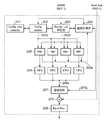
図1において、101は、図示していないホストコンピュータより転送された印刷コマンド・データを受信するHost_I/F_Logicである。このHost_I/F_Logic101は、DRAM_cont.102aを介して、受信された印刷コマンド・データをDRAM102へ格納する。尚、DMA_cont.102bは、DRAM102に格納されたDLをRasterize_mod.107に転送する場合などに使用される。
In FIG. 1,
106はCPUであり、後述するROM105に格納されたプログラムにしたがって印刷装置本体の全制御を行う演算・制御部である。CPU106は、各構成要素間の処理手順や同期制御、あるいは共通バスの制御(DMA_cont.と協働)を行なう。特に、CPU106はRasterize_mod.やShipping_mod.やVideo_I/F_LogicのYMCKプレーンに対する同期制御を行なう。尚、CPU106がRasterize_mod.107やData_compress109や拡大/縮小_mod.110やData_uncompress111などの処理を行なっても良いが、CPU106に負荷が集中して処理の高速化を妨げるので、Rasterize_mod.107の各planeそれぞれに、あるいはData_compress109や拡大/縮小_mod.110やData_uncompress111に共通、又はそれぞれに独立したCPUを有するのが望ましい。特に、本例では、Rasterize_mod.107の各planeそれぞれが独立したCPUを有して、他のplaneとは独立に展開処理を行なう(尚、同じObjectのplane間の同期はCPU106が制御する)。
102はDRAMで、ホストコンピュータからのコマンドおよびデータ等の受信データを一時的に蓄えるpageメモリである。あるいは前述のROM105内に記述されたプログラムに従って生成されるDLを格納するMainメモリとして使用される。また、Font cache領域として使用される。さらに前記の用途の他にCPU106が各プログラムを実行する際のワークエリアとしても使用される。105は、CPU106の制御プログラム、あるいは後述する図3及び図6に示すフローチャートによる一連の制御を実現するためのプログラムデータ、Fontデータなどを格納しているROMである。尚、図3及び図6に示すフローチャートはRasterize_mod.107の各planeの制御を示すものである。この制御はROM105から読出しながら動作するのではなく、Rasterize_mod.107の各plane(以下の図2参照)が有するRAM(Config._control202の制御やConfig._data_memory210と共有でもよい)にロードして実行されるのが望ましい。また、DMA_cont.105aは、ROM105に格納されたFontデータの読出しや、Rasterize_mod.107への制御プリグラムのロードなどで使用される。
A
103はHard_Disk、103aはHard_Disk_I/F_Logic、104はNV(non-volatile)RAM、104aはNVRAM_I/Fである。Hard Disk103及びNVRAM104は不揮発性の書換可能なメモリであり、大容量のデータや変更可能なプログラムなどが格納される。
103 is Hard_Disk, 103a is Hard_Disk_I / F_Logic, 104 is NV (non-volatile) RAM, and 104a is NVRAM_I / F. The
107は描画処理を実行する4つのplaneに分かれたRasterize_mod.である。Rasterize_mod.107は、DRAM102から読み込んだDLをROM105に格納されたプログラム(あるいはRasterize_mod.107にロードされたプログラム)に従ってbitmapデータへ展開し、Band Memory108へ格納する。109は前記のRasterize_mod.107が展開したデータを圧縮するData_compress_moduleである。110は縮小印字や文字の拡大処理を行うための拡大/縮小moduleである。111はBand Mem.108に格納された圧縮データを伸張するためのData_uncompress_moduleである。
また、112は,カラーの4-Drumエンジンの紙搬送に対応して画像データを前記Band Mem.108から読み出して、video_I/F_logic114へ出力するための同期回路(Shipping_mod.)である。113はプリンタエンジンを制御するcommand/statusの制御信号である。114,115はプリンタエンジンとそのI/F_logicである。116,117はプリンタの表示パネルとそのI/F_logicである。
<本実施形態の描画処理例>
次に、本実施形態の描画処理における、Object描画処理での属性の種類と、DL(Display List)の構成例、出力画像との関係について説明する。但し、本発明は描画処理におけるハードウエアリソースの再構成、その再構成のスケジューリング、更に動的スケジューリングに特徴があり、Object上が処理での属性の種類や、DLの構成例等に限定されるものではない。
<Example of drawing process of this embodiment>
Next, the relationship between the attribute type in the Object drawing process, the configuration example of DL (Display List), and the output image in the drawing process of the present embodiment will be described. However, the present invention is characterized by reconfiguration of hardware resources in rendering processing, scheduling of the reconfiguration, and dynamic scheduling, and the object is limited to the types of attributes in the processing, DL configuration examples, etc. It is not a thing.
(本実施形態における属性例)
本実施形態の描画回路においては、PDLを中間コード(DL)へ変換し、この中間コードが有する以下の4つの属性データを元にして描画イメージを生成するものとする。
(Example of attributes in this embodiment)
In the drawing circuit of this embodiment, PDL is converted into an intermediate code (DL), and a drawing image is generated based on the following four attribute data included in the intermediate code.
第1の属性は、描画オブジェクトの1つ1つについて印刷イメージ上で占有する領域データを示す属性データである。第2の属性は、多角形、円などの図形や文字の輪郭に代表されるような ForegroundとBackgroundとの境界を表す属性データである。第3の属性は、描画オブジェクトを塗りつぶす模様に代表されるようなForegroundの模様(あるいはBackgoundの色or模様)を示す属性データである。第4の属性は、その塗りつぶす色を示すForegroundの色(あるいはBackgroungの色or模様)を示す属性データである。 The first attribute is attribute data indicating area data occupied on the print image for each drawing object. The second attribute is attribute data representing the boundary between the Foreground and the Background as represented by the outline of a figure such as a polygon or a circle or the character. The third attribute is attribute data indicating a Foreground pattern (or Backgound color or pattern) as typified by a pattern for painting a drawing object. The fourth attribute is attribute data indicating the Foreground color (or Backgroung color or pattern) indicating the fill color.
ここで、Foregroundの色とは描画対象の主体の色を意味しており、文字などを描画する場合に文字自体に付けられる色を指している。Backgroundとは描画プレーン1つで2値データを扱う場合には描画を行うプレーンのハッチングパターンとなり、多値データを扱う場合にはフォアグランドの色を意味している。 Here, the Foreground color means the color of the subject to be drawn, and indicates the color attached to the character itself when drawing the character or the like. Background is a hatching pattern of a drawing plane when binary data is handled by one drawing plane, and the foreground color is meant when multi-value data is handled.
前記4種類の属性に基づくデータは、描画展開後に印刷する背景のイメージデータの上にそれぞれを重ねあわせる処理を行った後に、Band_Memory108へ格納される。図5は、あるオブジェクトについての各属性と描画処理の一例の概略を示したものである。
The data based on the four types of attributes is stored in the
(本実施形態におけるDLの構成例)
図9に、座標情報と描画objectの属性とを示した中間データ(display list)のコード例と構成例を示す。
(Example of DL configuration in this embodiment)
FIG. 9 shows a code example and a configuration example of intermediate data (display list) indicating coordinate information and attributes of a drawing object.
各リスト中でのaddr.指定は、データの管理上、pointer形式の間接指定になっている。例えばリスト中の"obj._addr._pointer#" (#: 1,2,3....)は各描画objectのHeaderを格納しているMemory_addr.を示すaddr._pointerである。ObjectのHeaderは、描画objectの種類(文字、図形、イメージ、背景データ、色データなど)を示すFunction_codeと幅・高さのパラメータ、及び、文字の圧縮code本体を格納しているMem.の先頭Addressを示すaddr._pointerから構成されている。 The addr. Specification in each list is an indirect specification in the pointer format for data management. For example, “obj._addr._pointer #” (#: 1, 2, 3,...) In the list is addr._pointer indicating Memory_addr. That stores the Header of each drawing object. Object Header is Function_code indicating the type of drawing object (character, figure, image, background data, color data, etc.), width / height parameters, and the head of Mem. It consists of addr._pointer indicating Address.
図9においては、Object_No.1とObject_No.2とがリストされている。 In FIG. 9, Object_No.1 and Object_No.2 are listed.
第1行から第7行まではObject_No.1の共通の属性である、領域及び形状(外形、輪郭)に係る情報である。第8行から第10行はObject_No.1のシアン(C)の属性、色(Color_Gradation)及び模様(Fill_Pattern)に係る情報である。第11行から第13行はObject_No.1のイエロー(Y)の属性、色及び模様に係る情報である。Object_No.1にはマゼンタ(M)とブラック(K)の情報は無い。 The first row to the seventh row are information related to the region and shape (outer shape, contour), which are common attributes of Object_No. The 8th to 10th lines are information related to the cyan (C) attribute, color (Color_Gradation), and pattern (Fill_Pattern) of Object_No. The eleventh to thirteenth lines are information relating to the attribute, color, and pattern of yellow (Y) of Object_No. Object_No. 1 has no information on magenta (M) and black (K).
第14行から第20行まではObject_No.2の共通の属性である、領域及び形状(外形、輪郭)に係る情報である。第21行から第23行はObject_No.2のシアン(C)の属性、色及び模様に係る情報である。第24行から第26行はObject_No.2のマゼンタ(M)の属性、色及び模様に係る情報である。Object_No.2にはイエロー(Y)とブラック(K)の情報は無い。 The 14th to 20th lines are information related to the region and shape (outer shape, outline), which are common attributes of Object_No.2. The 21st to 23rd lines are information related to the attribute, color, and pattern of cyan (C) of Object_No. The 24th to 26th lines are information related to the attribute, color, and pattern of magenta (M) of Object_No. Object_No. 2 has no information on yellow (Y) and black (K).
(本実施形態の出力画像の描画例)
図10は、図9の前記display listの各パラメータと実際の描画Objectとの関係を示す図である。同図において文字 "A", "A", "A", "S", "U"の各1文字がひとつの描画objectの単位となっている。以下に、図9の値と図10の関係を簡単に説明する。図9はObject_No.1とObject_No.2しか記載されていないので、これらは図10の左の文字 "A",と次の文字"A"に対応させて説明する。
(Drawing example of output image of this embodiment)
FIG. 10 is a diagram showing the relationship between each parameter of the display list of FIG. 9 and the actual drawing object. In the figure, each character “A”, “A”, “A”, “S”, “U” is a unit of one drawing object. The relationship between the values in FIG. 9 and FIG. 10 will be briefly described below. FIG. 9 shows only Object_No. 1 and Object_No. 2, so these will be described in correspondence with the left letter “A” and the next letter “A” in FIG. 10.
図9の第2行の描画高さ(Ha1)と幅(Wa1)とが、図10の最初の文字 "A"の高さ(Ha)と幅(Wa)とにそれぞれ対応する。ここでは、各文字の高さ及び幅は同じなので、Object_No.1の高さ(Ha1)及び幅(Wa1)を示す値とObject_No.2の高さ(Ha2)及び幅(Wa2)を示す値とは等しい。第3行の描画開始座標(Xa1,Ya1)は図10のXa,Yaである。更に、第4行のOffset座標(Off_Xa1,Off_Ya1)は図10のOff_Xa1,Off_Ya1に相当する。すなわち、最小の文字 "A"の描画開始位置(領域の左上)は、図10の描画座標基準点からX方向(右方向)に(Xa+Off_Xa1)、Y方向(下方向)に(Ya+Off_Ya)である。ここで、Xa1=Xa2, Ya1=Ya2, Off_Ya1=Off_Ya2なので図10ではXa, Ya, Off_Yaと表示している。 The drawing height (Ha1) and width (Wa1) of the second line in FIG. 9 correspond to the height (Ha) and width (Wa) of the first character “A” in FIG. Here, since the height and width of each character are the same, the value indicating the height (Ha1) and width (Wa1) of Object_No.1 and the value indicating the height (Ha2) and width (Wa2) of Object_No.2. Are equal. The drawing start coordinates (Xa1, Ya1) of the third line are Xa, Ya in FIG. Furthermore, the Offset coordinates (Off_Xa1, Off_Ya1) in the fourth row correspond to Off_Xa1, Off_Ya1 in FIG. That is, the drawing start position (upper left of the area) of the minimum character “A” is (Xa + Off_Xa1) in the X direction (right direction) and (Ya + Off_Ya) in the Y direction (down direction) from the drawing coordinate reference point in FIG. . Here, since Xa1 = Xa2, Ya1 = Ya2, Off_Ya1 = Off_Ya2, Xa, Ya, Off_Ya are displayed in FIG.
この描画開始位置(Xa+Off_Xa1, Ya+Off_Ya)から高さ(下方向)Ha, 幅(右方向)Waの矩形が属性の「領域」に相当する。 A rectangle having a height (downward direction) Ha and a width (rightward direction) Wa from the drawing start position (Xa + Off_Xa1, Ya + Off_Ya) corresponds to an attribute “region”.
第5行のobj._addr._pointer1の先のObject_HeaderからObj._Func.が文字(フォントの種類なども含む)を特定する情報である。幅(width)及び高さ(Height)は領域の幅及び高さと同じである。、また、Obj._Body_addr._pointerが指し示すobjectの形状の圧縮dataとして文字"A"の圧縮データがObject_NO.1_codeに記憶されている。このObject_NO.1_codeが属性の「外形(輪郭)」に相当する。 Obj._Func. Is information for specifying characters (including font type) from Object_Header ahead of obj._addr._pointer1 in the fifth line. The width (width) and height (Height) are the same as the width and height of the region. In addition, compressed data of the character “A” is stored in Object_NO.1_code as compressed data of the shape of the object indicated by Obj._Body_addr._pointer. This Object_NO.1_code corresponds to the attribute “outline (contour)”.
そして、上述のColor_Gradiationが属性の「色」に、Fill_Patternが属性の「模様」に相当する。 The above-described Color_Gradiation corresponds to the attribute “color” and Fill_Pattern corresponds to the attribute “pattern”.
次のObject_No.2の文字"A"についても、上記の構成とほぼ同様である。但し、Object_No.1の文字"A"とは色が異なる。尚、図9には第18行のobj._addr._pointer2がObject_NO.2_codeを指し示すように図示されているが、図10のように同じ文字"A"の場合は、Object_NO.1_codeを指し示す。 The character “A” of the next Object_No. 2 is almost the same as the above configuration. However, the color is different from the character “A” of Object_No. In FIG. 9, obj._addr._pointer2 in the 18th line is shown as pointing to Object_NO.2_code, but in the case of the same character “A” as shown in FIG. 10, it indicates Object_NO.1_code.
(本実施形態における展開処理の分割例)
次に、本実施形態における展開処理をどのように分割して、複数のリコンフィギュラブルプロセッサで実行できるのかを説明する。
(Example of division of expansion processing in this embodiment)
Next, how the expansion processing in this embodiment can be divided and executed by a plurality of reconfigurable processors will be described.
本実施形態の展開処理は、基本的にライン単位である。すなわち、どの属性においても中間データはライン単位で一区切りとなるような構造になっている。従って、ページデータをライン単位で分割し、展開処理可能な構成である。その場合に、例えば「色(BG)」においては縦64pixel×横64Pixelの矩形領域単位で分割が可能である。又、「輪郭(MSK)」の処理においては、line_skip機能が備わっている。このline_skip機能とは、例えば展開領域の上半分のラインと下半分のラインを分割しても、上半分のラインを読み飛ばして下半分のラインの先頭から展開を可能とする機能である。 The unfolding process of this embodiment is basically in line units. That is, in any attribute, the intermediate data is structured so as to be separated into one line unit. Therefore, the page data is divided in line units and can be expanded. In this case, for example, “color (BG)” can be divided in units of a rectangular area of 64 pixels vertically × 64 pixels horizontally. In the “contour (MSK)” process, a line_skip function is provided. The line_skip function is a function that enables development from the top of the lower half line by skipping the upper half line even if the upper half line and the lower half line of the development area are divided, for example.
以上説明したように、本実施形態ではライン単位の分割という規則による制限があるが、これは一例であり他の分割が可能な展開であればどのような処理でもよく、これらも本発明に含まれる。 As described above, in the present embodiment, there is a restriction by the rule of division in line units, but this is an example, and any processing may be performed as long as other division is possible, and these are also included in the present invention. It is.
<本実施形態の描画処理回路の構成例>
図2は、図1におけるK, Y, M, C-plane用の描画処理回路であるRasterize_moduleの構成例を示したものである。前記各plane毎にこの図2で示す回路があり、計4個存在している。以下に各構成要素について説明を行う。
<Configuration Example of Drawing Processing Circuit of this Embodiment>
FIG. 2 shows a configuration example of Rasterize_module which is a drawing processing circuit for K, Y, M, C-plane in FIG. There is a circuit shown in FIG. 2 for each plane, and a total of four circuits exist. Each component will be described below.
図2において、205に示されているRM1〜RM4は、本実施形態で使用するリコンフィギュラブルプロセッサモジュール(再構成可能な処理回路モジュールの意)である。RMが行う処理については後述する。206は前記RM1〜RM4からの出力データを格納するためのFIFOである。FIFO206は、RM1〜RM4が描画領域の描画開始位置(通常、左上)からPixel単位(描画画素単位)に展開した出力データを順に記憶する。また、201は描画回路を再構成するためのデータを格納しているConfig._data_memoryである。202は前記データをRM1〜RM4のどのリコンフィギュラブルプロセッサにloadするかを監視し、前記memoryからデータを読み出して各モジュールの回路再構成を制御している制御部(Config._control)である。尚、Config._data_memory201には、Config._control202がRM1〜RM4をリコンフィギュアするスケジュールを管理するプログラムも格納されている。
In FIG. 2, RM1 to RM4 indicated by 205 are reconfigurable processor modules (meaning reconfigurable processing circuit modules) used in the present embodiment. Processing performed by the RM will be described later.
203はPDL(プリンタ記述言語)から変換された中間コード(display list;図9参照)を解析して、描画Objectの属性毎にRM1〜RM4で描画展開が可能なデータ(あるいは対応する中間コードそのままでもよい)を作成するDisplay_List解析部である。204は前記中間コードから各属性毎の描画展開に係る処理時間を予測し、後述の描画演算処理部207から進行状況のフィードバックをうけて、予測時間の補正を行う描画計測部である。描画演算処理部207は、前記RM1〜RM4が展開した各属性毎の描画データをdisplay listに記載されている描画論理に従って、レイヤーのon/off、重ね合わせなどの演算をpixel単位で行う描画演算部である。208は前記の演算を行ったデータをプリンタエンジンに送出する前段のbufferであるBand_Mem.を示す。
203 analyzes the intermediate code (display list; see FIG. 9) converted from PDL (printer description language), and can be rendered with RM1 to RM4 for each attribute of the rendered object (or the corresponding intermediate code as it is) It is a Display_List analysis unit that creates (may be). A drawing
ここで、図1のBand_Mem.108は、少なくともBand_Mem.208が4plane分記憶できる容量が必要である。高速処理のためにバッファすることを考慮すると8plane分を用意するのが好適である。209は、図1のHard_Disk103などにオペレータによって予め格納してある図5の背景データ(例えば、フォームオーバーレイ、社標のロゴ、すかし文字、罫線など)を、展開処理されたホストからの描画データに重ね合わせるための加算器である。
Here, Band_Mem. 108 in FIG. 1 needs to have a capacity that at least Band_Mem. 208 can store four planes. In consideration of buffering for high-speed processing, it is preferable to prepare 8 planes.
尚、FIFO206にRM1〜RM4で展開処理したデータをどのように記憶し、描画演算処理部207でどのようにビット単位で合成するかについては、以下のような種々の方法があり、どの方法をとっても構わない。
(1) RM1〜RM4より出力するデータの先頭に属性とObject_Noを識別可能なタグを付けて識別する。
(2) 図2のconfig._Cotrol202からBPU207に対して描画Obj. No.と各RMで処理している属性の種類の対応を示す信号を出力する。
(3) RMの後段にあるFIFO206を領域、輪郭、色、模様の各1つずつに割り当てておき、BPU207は例えばFIFO_1からFIFO_4までそれぞれから読み出したデータと前記属性と対応させる。
There are the following various methods for storing the data expanded by RM1 to RM4 in the
(1) Attach a tag that can identify the attribute and Object_No at the beginning of the data output from RM1 to RM4.
(2) A signal indicating the correspondence between the drawing Obj. No. and the attribute type processed by each RM is output from the
(3) The
又、図2では、Config._control202や、Display_List解析部203、描画計測部204、描画演算部207などを独立した構成要素として図示しているが、これらはCPUとmemoryとで構成された共通のコンピュータでソフト的に実現するものでよい。その場合に、Config._data_memory201や、CPUのプログラムがロードされるmemory、Display_Listをロードするmomoryなどは、1つのmemoryを共有してもよい。
In FIG. 2,
(リコンフィギュラブルプロセッサモジュール)
ここで、リコンフィギュラブルプロセッサモジュールについて簡単に説明を行う。
(Reconfigurable processor module)
Here, the reconfigurable processor module will be briefly described.
リコンフィギュラブルプロセッサと称されるものは動的再構成(再構築)可能な論理装置である。これらは、機能分けされた専用回路ではなく、あらかじめ用意した複数の必要な回路の接続構成と動作設定をソフトウェアによって切り替えることで、専用回路と同等の機能を実現するものである。また、動作中にもそうした切り替えを可能とする特徴をも有するものがある。特に、動的に再構成が可能なリコンフィギュラブルプロセッサは、ダイナミックリコンフィギュラブルプロセッサと称されることが多い。 What is called a reconfigurable processor is a logic device that can be dynamically reconfigured (reconstructed). These are not dedicated circuits with different functions, but realize a function equivalent to that of a dedicated circuit by switching connection configurations and operation settings of a plurality of necessary circuits prepared in advance by software. Some have a feature that enables such switching during operation. In particular, a reconfigurable processor that can be dynamically reconfigured is often referred to as a dynamic reconfigurable processor.
一般的に、ダイナミックリコンフィギュラブルプロセッサは、チップ(論理装置)内に必要な回路を部分的にユニット化したハードウエア要素を予め複数準備する。そして、ユニットの選択や接続順序、動作設定といったパラメータやプログラムを事前にメモリに格納しておき、その格納したプログラムやパラメータをソフトウェアによって動作中に瞬時に切り替えることにより、処理内容に応じて専用回路をもつチップのように振舞うものである。つまり、本実施形態のリコンフィギュラブルプロセッサ(RM)は、パラメータやプログラムを切り替えることで、たとえば、領域(AR)用描画回路として動作させた後に、輪郭(MSK)用描画回路として再構成させ、動作させることも可能となる。 Generally, a dynamic reconfigurable processor prepares in advance a plurality of hardware elements in which necessary circuits are partially unitized in a chip (logic device). Then, parameters and programs such as unit selection, connection order, and operation settings are stored in memory in advance, and the stored programs and parameters are switched instantaneously during operation by software, so that a dedicated circuit can be used according to the processing content. It behaves like a chip with In other words, the reconfigurable processor (RM) of the present embodiment can be reconfigured as a contour (MSK) drawing circuit, for example, after operating as a region (AR) drawing circuit by switching parameters and programs, It can also be operated.
こうした思想に基づく技術は、FPGAなどに代表されるように古くから存在しているが、ダイナミックリコンフィギュラブルプロセッサは、集積度の向上や動的な切り替えが実現できる高速性において、FPGAよりも優れている。 Technologies based on these ideas have existed for a long time, as represented by FPGAs, etc., but dynamic reconfigurable processors are superior to FPGAs in terms of high speed that can improve integration and dynamically switch. ing.
FPGAを構成するコンポーネントはゲートアレイであるため、実行できる処理も予め有する論理ゲート相当の機能となる。これに対してリコンフィギュラブルプロセッサを構成するユニットは小規模なプロセッサ相当か、プロセッサデータパス内の機能ブロック相当であるのが一般的となっている。そのため、当然ながらFPGAに比べてリコンフィギュラブルプロセッサの方が、高度な処理を実現可能である。 Since the component constituting the FPGA is a gate array, it has a function equivalent to a logic gate that has a process that can be executed in advance. On the other hand, the units constituting the reconfigurable processor are generally equivalent to a small-scale processor or a functional block in the processor data path. Therefore, as a matter of course, the reconfigurable processor can realize a higher level of processing than the FPGA.
なお、本発明を説明するためのいくつかの実施形態では、描画回路としてダイナミックリコンフィギュラブル技術を採用しているが、同様の処理が可能な構成であればこれに限定されない。 In some embodiments for explaining the present invention, a dynamic reconfigurable technique is adopted as a drawing circuit, but the present invention is not limited to this as long as the same processing can be performed.
<本実施形態の描画処理回路の動作例>
図3は、前記図1及び図2で示されるような画像出力制御装置において、各描画処理回路の再構成の手順例を示したフローチャートである。本実施形態では、この手順は各描画処理回路の独立したCPUで実行されるのが好ましいが、各構成要素がそれぞれのステップを実行する構成であっても、高速であって負担がなければ図1のCPU106が実行してもよい。
<Operation Example of Drawing Processing Circuit of Present Embodiment>
FIG. 3 is a flowchart showing an example of the reconfiguration procedure of each drawing processing circuit in the image output control apparatus as shown in FIGS. In this embodiment, this procedure is preferably executed by an independent CPU of each drawing processing circuit. However, even if the configuration is such that each component executes each step, the procedure is fast and has no burden. One
まず、ステップS301において該当Band内の描画Objectの属性から図2の描画計測部204が1Bandの描画あたりに要する描画処理時間を見積もる。そして、ステップS302において各描画Object毎に描画回路での処理時間を予測する。この予測結果を基にして、ステップS303で描画回路をどのように再構成(リコンフィギュレーション)するかについての順番を、図2のconfig._Control部202でスケジューリングし、その情報(スケジューリングデータ)を図2のconfig._Data_memory201へ格納する。
First, in step S301, the drawing
そして、ステップS304で、前記スケジューリングデータに従って1個目の描画Objectを描画するために必要な描画回路のコンフィギュレーションデータを図2のconfig._Data_memory201から読み出して、図2のRM1〜RM4を構成する。そして、ステップS305で描画ハードウエアを起動する。ハードウエアが起動すると、コンフィギュレーションデータに基づいて構成されたRM1〜RM4が各描画Object毎の属性に応じた描画データの展開を開始し、展開が終了したデータを図2のFIFO206へ順次格納していく。
Then, in step S304, the configuration data of the drawing circuit necessary for drawing the first drawing object according to the scheduling data is read from
また、ステップS306では、RM1〜RM4の各moduleからのステータス信号を受けて、描画処理が早めに終了しているものがないかを判定する。なお、このステップは図2の描画計測部204が実行する。その後、ステップS307では、前記描画計測部204からの予測情報と現状の処理ステータス(描画実行中 or 描画終了)を受けて、未だ描画処理に時間がかかるようなobjectの属性のものがあるか否かを判断する。そして、特定の属性のものが他の属性に比べて処理時間がかかると予測される場合には、ステップS308で負荷を分散するように図2のconfig._Data_memory201に格納されているスケジューリングデータを修正し、これに基づいてステップS304からの処理を再度行う。
Also, in step S306, it is determined whether or not there is any drawing process that has been completed early by receiving a status signal from each of the modules RM1 to RM4. This step is executed by the drawing
一方、ステップS306で描画処理が早めに終了しているものが無い、またはステップS307でボトルネックとなるような属性を持った描画Objectが無いと判断された場合には、ステップS309で描画論理演算(BPU)を実行し、当該描画objectの処理を終了する。その後、ステップS311で現在描画処理をしているBandにおいて全ての描画Objectの展開が終了するまでチェックをし、繰り返し前記の処理を行うものである。 On the other hand, if it is determined in step S306 that there is no drawing process that has been completed early, or that there is no drawing object having an attribute that becomes a bottleneck in step S307, a drawing logical operation is performed in step S309. (BPU) is executed, and the processing of the drawing object ends. After that, in step S311, a check is performed until development of all drawing objects is completed in the band currently being drawn, and the above-described processing is repeated.
(本実施形態の描画処理のタイミング例)
図4の下段は、図3のフローチャートに従ってスケジューリングを修正して描画回路(RM)の再構成を行う場合について、従来の固定した回路構成での処理時間(図4の上段)と比較して示したものである。RM1〜RM4は、描画Objectの属性である領域データ(AR)、輪郭データ(MSK)、色データ(BG)、模様データ(GD)を並列で処理するためのリコンフィギュラブルな回路モジュールである。タイミングチャートの横軸が、各RM1〜RM4が各々の処理に要する時間を示している。
(Example of timing of drawing processing of this embodiment)
The lower part of FIG. 4 shows the case of reconfiguring the drawing circuit (RM) by modifying the scheduling according to the flowchart of FIG. 3 in comparison with the processing time in the conventional fixed circuit configuration (upper part of FIG. 4). It is a thing. RM1 to RM4 are reconfigurable circuit modules for processing region data (AR), contour data (MSK), color data (BG), and pattern data (GD), which are attributes of the drawing object, in parallel. The horizontal axis of the timing chart indicates the time required for each process by each RM1 to RM4.
図4の上段に記載している従来例においては、描画Object1を描画する際において、例えばRM1やRM2の「領域(AR)」と「輪郭(MSK)」の処理が早く終了しても、RM4の「模様(GD)」の処理が終わるまでは図2の描画演算モジュール: Bit Processing Uint207で次のObject 2の描画処理を開始できないため、待たされる状態(idle状態)になっていた。
In the conventional example described in the upper part of FIG. 4, even when the processing of “area (AR)” and “contour (MSK)” of RM1 and RM2 ends early when drawing Object1, for example, RM4 Until the processing of “pattern (GD)” of FIG. 2 is completed, the drawing processing module: Bit Processing Uint 207 in FIG. 2 cannot start the drawing processing of the
一方、図4の下段に記載している本実施形態の例では、従来例で描画処理が早く終了したRM1, RM2などのモジュールについては、回路の再構成が行われたことによって、描画Object1の展開処理が従来例よりも早く終了し、最終的に描画Object2についての描画演算モジュール(BPU)の処理を早く開始することが可能となる。以下、描画Object 2,3,4...についても同様である。 On the other hand, in the example of the present embodiment described in the lower part of FIG. 4, for the modules such as RM1 and RM2 for which the drawing process was completed earlier in the conventional example, the circuit is reconfigured, so that the drawing Object1 The unfolding process ends earlier than in the conventional example, and finally the drawing operation module (BPU) process for drawing Object2 can be started earlier. The same applies to the drawing objects 2, 3, 4,.
このように、本発明を適用することにより、描画Object1〜4までに要する時間が従来の固定した処理回路の場合と比較して処理時間を大幅に短縮することが可能となる。
As described above, by applying the present invention, it is possible to significantly reduce the processing time as compared with the case of the conventional processing circuit in which the time required for drawing
具体的には、PDLを解析して中間コード(display list)に変換した後の描画処理をハードウエアの固定した処理によって行うのではなく、実際の回路の処理時間と処理に必要なデータサイズを鑑みて動的に回路構成を変更することにより、1Bandあたりの描画ObjectをBit Map Dataへ展開するために要する処理時間を短縮させるという効果がある。 Specifically, the rendering process after the PDL is analyzed and converted to an intermediate code (display list) is not performed by hardware fixed processing, but the actual circuit processing time and data size required for processing are determined. In view of this, by dynamically changing the circuit configuration, there is an effect of shortening the processing time required to develop the drawing object per band into the bit map data.
尚、図4の下段の再構成はかなりの時間幅で表示しているが、実際の再構成の処理はシステムクロックの1cycleで実現でき、全体の処理にははとんど影響しない。RM1〜RM4の再構成は、ソフトプログラムとパラメータを入れ替えるものであっても、一部ハードウエアの選択や繋ぎ変えなどを含んでもよい。 Although the reconfiguration in the lower part of FIG. 4 is displayed with a considerable time width, the actual reconfiguration process can be realized in one cycle of the system clock, and the entire process is hardly affected. The reconfiguration of RM1 to RM4 may replace software programs and parameters, or may include selection of some hardware or reconnection.
<本実施形態の描画処理回路の他の動作例>
上記実施形態においては、描画回路を再構成する際の判断基準として各属性の描画が終了したという実時間の処理状態を元にしてスケジューリング、あるいは見積もり時間の補正をしていた。本実施形態の動作例では予め各属性に係る描画処理時間を見積もった後で、負荷(時間)のかかる属性の回路を優先的に再構成をするというものである。
<Another operation example of the drawing processing circuit of this embodiment>
In the above-described embodiment, scheduling or correction of estimated time is performed based on a real-time processing state that drawing of each attribute is completed as a criterion for reconfiguring the drawing circuit. In the operation example of this embodiment, after preliminarily estimating the drawing processing time for each attribute, the circuit having the attribute that requires a load (time) is preferentially reconfigured.
図6は、本実施形態の処理手順を示すフローチャートであり、以下順を追って処理を説明する。 FIG. 6 is a flowchart showing the processing procedure of the present embodiment, and the processing will be described in order.
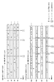
まず、ステップS601で描画Objectの属性から描画処理時間を見積もり、ステップS602で各Objectの属性毎の処理時間をtotalデータとして格納しておく。 First, in step S601, the drawing processing time is estimated from the drawing object attribute, and in step S602, the processing time for each object attribute is stored as total data.
図7は、図6のステップS602で格納しているtotalデータの例である。図7において、1 Band目はN個の描画Objectが存在し、2 Band目にはM個の描画Objectが存在するものとする。各Object毎の描画処理時間の予測値を格納した後で、各BandにおいてA.領域、B. 輪郭、 C. 色、 D.模様の各属性毎の描画処理時間の合計を示すtotal_time(実際はsystem clockのサイクル数で表す)についても予測を行う。次に、前記のtotalデータを基にして、ステップS603で描画回路を再構成する順番をスケジューリングし、ステップS604で前記totalデータに格納されているtotal_timeの大きい属性のものから優先的に回路の再構成を行う順番を決定する。 FIG. 7 is an example of the total data stored in step S602 of FIG. In FIG. 7, it is assumed that there are N drawing objects in the first band and M drawing objects in the second band. After storing the predicted value of the rendering processing time for each object, total_time indicating the total rendering processing time for each attribute of A. area, B. contour, C. color, and D. pattern in each Band (actually system Prediction is also made for clock cycles). Next, based on the total data, schedule the order in which the drawing circuit is reconfigured in step S603, and in step S604, the circuit is reconfigured preferentially from the attribute having the large total_time stored in the total data. Decide the order in which to configure.
そして、この結果は、図2のConfig._data_memory201へ格納された後に、ステップS605で描画ハードウエアが起動される。ハードウエアが起動されると、RM1〜RM4が各描画Object毎の属性に応じた描画データの展開処理を開始し、展開が終了したデータを図2のFIFO206へ順次格納していく。また、図2の描画計測部204はRM1〜RM4までの各moduleからのステータス信号を受けて、ステップS606で描画処理が早めに終了しているものがないかをセンスする。その後、前記描画計測部204からの予測情報と現状の処理ステータス(描画実行中 or 描画終了)を受けて、ステップS607で現在のBandにおいて描画処理のtotal_time=0 (system cycle)のものが存在するか否かを判断する。ここで、total_time = 0となる属性のものが存在する場合には、ステップS608で負荷を分散するように図2のconfig. Data memory201に格納されているスケジューリングデータを修正し、これに基づいてステップS604からの処理を再度行う。
Then, after this result is stored in Config._data_memory 201 in FIG. 2, the drawing hardware is started in step S605. When the hardware is activated, RM1 to RM4 start drawing data expansion processing corresponding to the attributes of each drawing object, and the expansion-completed data is sequentially stored in the
一方、ステップS606で描画処理が早めに終了しているものが無い、またはステップS607でボトルネックとなるような属性を持った描画Objectが無いと判断された場合には、ステップS609でBPUの描画論理演算を実行し、当該描画objectの処理を終了する。その後、ステップS611で現在描画処理をしているBandにおいて全ての描画Objectの展開が終了するまでチェックをし、繰り返し前記の処理を行うものである。 On the other hand, if it is determined in step S606 that there is no drawing process that has been completed early or there is no drawing object having an attribute that becomes a bottleneck in step S607, the drawing of the BPU is performed in step S609. The logical operation is executed, and the processing of the drawing object is finished. After that, in step S611, a check is made until the development of all the drawn objects is completed in the band currently being drawn, and the above processing is repeated.
(本実施形態の描画処理のタイミング例)
図8は、図6のフローチャートにともづいて、図2のRP1〜RP4までの回路を再構成したときの例を示したものである。
(Example of timing of drawing processing of this embodiment)
FIG. 8 shows an example when the circuits from RP1 to RP4 in FIG. 2 are reconfigured according to the flowchart in FIG.
先の実施形態で示した図4との違いは、obj.1の処理において最も処理時間を要する属性である「模様(GD)」「色(BG)」から再構成を行い、それが終了した後で属性「領域(AR)」「輪郭(MSK)」の処理回路を再構成している点である。 The difference from FIG. 4 shown in the previous embodiment is that reconstruction is performed from “pattern (GD)” and “color (BG)”, which are attributes that require the most processing time in the processing of obj.1. The point is that the processing circuits of the attributes “Area (AR)” and “Outline (MSK)” are reconfigured later.
このように再構成のスケジューリングを実行することで、さらに展開処理を高速に実行することができる。 By executing the reconfiguration scheduling in this way, the expansion process can be executed at a higher speed.
Claims (6)
前記描画オブジェクト生成手段が生成した描画オブジェクトデータをビットマップデータに展開するための複数の展開手段であって、前記属性データの種類に応じた複数種類の展開処理を実行するために動的に再構成可能なプロセッサを有する複数の展開手段と、
前記展開処理を実行する前に、前記複数の展開手段の各々に割り当てられた属性データに基づいて前記割り当てられた属性データを前記複数の展開手段の各々が展開処理するのに要する処理時間を見積り、前記複数の展開手段のアイドル状態を少なくするように前記プロセッサが実行する展開処理の種類を切り替えるためのスケジューリングデータを生成するスケジューリングデータ生成手段と、
該スケジューリングデータに基づいて、前記プロセッサが実行する展開処理の種類を切り替えるよう前記プロセッサを再構成する再構成手段とを有し、
特定の描画オブジェクトデータに含まれる複数の属性データを処理する際に、前記複数の展開手段に含まれる特定の展開手段に割り当てられた属性データの展開処理が終了し、かつ前記複数の展開手段に含まれる他の展開手段に割り当てられた属性データの展開処理が終了していない場合に、
前記スケジューリングデータ生成手段は、前記他の展開手段に割り当てられた属性データの展開処理を前記特定の展開手段に実行させるべく、前記スケジューリングデータを修正し、
前記再構成手段は、前記修正されたスケジューリングデータに基づいて、前記特定の展開手段が有するプロセッサが実行する展開処理の種類を前記他の展開手段が有するプロセッサが実行する展開処理の種類に切り替えるよう前記特定の展開手段が有するプロセッサを再構成することを特徴とする描画処理回路。 It receives data described in a page description language, and drawing object generating means for generating a drawing object data containing multiple attribute data each representing a different attribute possessed by the described drawing object by the data thus received,
A plurality of expansion means for expanding the drawing object data generated by the drawing object generation means into bitmap data, wherein the drawing object data is dynamically regenerated to execute a plurality of types of expansion processing according to the type of the attribute data; A plurality of deployment means having a configurable processor;
Before executing the expansion process, the processing time required for each of the plurality of expansion means to expand the assigned attribute data is estimated based on the attribute data allocated to each of the plurality of expansion means. Scheduling data generation means for generating scheduling data for switching the type of expansion processing executed by the processor so as to reduce the idle state of the plurality of expansion means;
Based on the scheduling data, possess a reconstruction means for reconstructing the processor to switch the type of development processing said processor executes,
When processing the plurality of attribute data included in the specific drawing object data, the expansion processing of the attribute data assigned to the specific expansion unit included in the plurality of expansion units ends, and the plurality of expansion units If the expansion process of attribute data assigned to other expansion means included is not finished,
The scheduling data generation means modifies the scheduling data to cause the specific expansion means to execute expansion processing of attribute data assigned to the other expansion means,
The reconfiguring means switches the type of the expansion process executed by the processor included in the specific expansion means to the type of the expansion process executed by a processor included in the other expansion means based on the modified scheduling data. A drawing processing circuit, wherein a processor included in the specific expansion unit is reconfigured .
前記スケジューリングデータ生成手段は、前記処理時間判定手段が判定した前記属性データの種類毎の処理時間に基づいて、前記複数の展開手段が前記複数の属性データの前記展開処理を終了する時間が各属性データで略同じとなるように、前記スケジューリングデータを修正することを特徴とする請求項1記載の描画処理回路。 A processing time for determining, for each type of attribute data, a processing time required to execute a development process for developing a plurality of attribute data of the same type included in a plurality of drawing objects into bitmap data based on the scheduling data Having a judging means ,
The scheduling data generating means is configured to determine, based on the processing time for each type of the attribute data determined by the processing time determining means, the time when the plurality of expanding means finish the expanding process of the plurality of attribute data for each attribute. as will be substantially the same in the data, the drawing processing circuit according to claim 1, wherein the benzalkonium be modified the scheduling data.
前記描画処理回路が、
ページ記述言語で記述されたデータを受信して、該受信したデータにより記述された描画オブジェクトが有する異なる属性をそれぞれ表現する複数の属性データを含む描画オブジェクトデータを生成する描画オブジェクト生成手段と、
前記生成手段が生成した描画オブジェクトデータをビットマップデータに展開するための複数の展開手段であって、前記属性データの種類に応じた複数種類の展開処理を実行するために動的に再構成可能なプロセッサを有する複数の展開手段と、
前記展開処理を実行する前に、前記複数の展開手段の各々に割り当てられた属性データに基づいて前記割り当てられた属性データを前記複数の展開手段の各々が展開処理するのに要する処理時間を見積り、前記複数の展開手段のアイドル状態を少なくするように前記プロセッサが実行する展開処理の種類を切り替えるためのスケジューリングデータを生成するスケジューリングデータ生成手段と、
該スケジューリングデータに基づいて、前記プロセッサが実行する展開処理の種類を切り替えるよう前記プロセッサを再構成する再構成手段とを有し、
特定の描画オブジェクトデータに含まれる複数の属性データを処理する際に、前記複数の展開手段に含まれる特定の展開手段に割り当てられた属性データの展開処理が終了し、かつ前記複数の展開手段に含まれる他の展開手段に割り当てられた属性データの展開処理が終了していない場合に、
前記スケジューリングデータ生成手段は、前記特定の展開手段とは異なる他の展開手段に割り当てられた属性データの展開処理を前記特定の展開手段に実行させるべく、前記スケジューリングデータを修正し、
前記再構成手段は、前記修正されたスケジューリングデータに基づいて、前記特定の展開手段が有するプロセッサが実行する展開処理の種類を前記他の展開手段が有するプロセッサが実行する展開処理の種類に切り替えるよう前記特定の展開手段が有するプロセッサを再構成することを特徴とする画像出力制御装置。 An image output control apparatus that has a drawing processing circuit that receives data described in a page description language and expands the bitmap data into bitmap data, and outputs the bitmap data expanded by the drawing processing circuit to an output unit,
The drawing processing circuit
It receives data described in a page description language, and drawing object generating means for generating a drawing object data containing multiple attribute data each representing a different attribute possessed by the described drawing object by the data thus received,
A plurality of expansion means for expanding the drawing object data generated by the generation means into bitmap data, which can be dynamically reconfigured to execute a plurality of types of expansion processing according to the type of the attribute data A plurality of deployment means having various processors;
Before executing the expansion process, the processing time required for each of the plurality of expansion means to expand the assigned attribute data is estimated based on the attribute data allocated to each of the plurality of expansion means. Scheduling data generation means for generating scheduling data for switching the type of expansion processing executed by the processor so as to reduce the idle state of the plurality of expansion means;
Based on the scheduling data, possess a reconstruction means for reconstructing the processor to switch the type of development processing said processor executes,
When processing the plurality of attribute data included in the specific drawing object data, the expansion processing of the attribute data assigned to the specific expansion unit included in the plurality of expansion units ends, and the plurality of expansion units If the expansion process of attribute data assigned to other expansion means included is not finished,
The scheduling data generation means modifies the scheduling data to cause the specific expansion means to execute expansion processing of attribute data assigned to another expansion means different from the specific expansion means,
The reconfiguring means switches the type of the expansion process executed by the processor included in the specific expansion means to the type of the expansion process executed by a processor included in the other expansion means based on the modified scheduling data. An image output control apparatus, comprising: reconfiguring a processor included in the specific expansion unit .
前記スケジューリングデータ生成手段は、前記処理時間判定手段が判定した前記属性データの種類毎の処理時間に基づいて、前記複数の展開手段が前記複数の属性データの前記展開処理を終了する時間が各属性データで略同じとなるように、前記スケジューリングデータを修正することを特徴とする請求項5記載の画像出力制御装置。 The drawing processing circuitry, based on said scheduling data, the type of the attribute data processing time required to perform the expansion process of expanding the same kind of a plurality of attribute data to the bit map data included in a plurality of drawing objects A processing time determination means for determining each time ,
The scheduling data generating means is configured to determine, based on the processing time for each type of the attribute data determined by the processing time determining means, the time when the plurality of expanding means finish the expanding process of the plurality of attribute data for each attribute. as will be substantially the same in the data, the image output control apparatus according to claim 5, wherein the benzalkonium be modified the scheduling data.
Priority Applications (2)
| Application Number | Priority Date | Filing Date | Title |
|---|---|---|---|
| JP2004275029A JP4405884B2 (en) | 2004-09-22 | 2004-09-22 | Drawing processing circuit and image output control device |
| US11/231,833 US7821656B2 (en) | 2004-09-22 | 2005-09-22 | Method of drawing images using a dynamic reconfigurable processor, circuit therefor and image output control apparatus |
Applications Claiming Priority (1)
| Application Number | Priority Date | Filing Date | Title |
|---|---|---|---|
| JP2004275029A JP4405884B2 (en) | 2004-09-22 | 2004-09-22 | Drawing processing circuit and image output control device |
Publications (3)
| Publication Number | Publication Date |
|---|---|
| JP2006088433A JP2006088433A (en) | 2006-04-06 |
| JP2006088433A5 JP2006088433A5 (en) | 2009-09-17 |
| JP4405884B2 true JP4405884B2 (en) | 2010-01-27 |
Family
ID=36073602
Family Applications (1)
| Application Number | Title | Priority Date | Filing Date |
|---|---|---|---|
| JP2004275029A Expired - Fee Related JP4405884B2 (en) | 2004-09-22 | 2004-09-22 | Drawing processing circuit and image output control device |
Country Status (2)
| Country | Link |
|---|---|
| US (1) | US7821656B2 (en) |
| JP (1) | JP4405884B2 (en) |
Families Citing this family (32)
| Publication number | Priority date | Publication date | Assignee | Title |
|---|---|---|---|---|
| EP1508235B1 (en) * | 2002-05-29 | 2009-03-11 | Panasonic Corporation | Data transmitting apparatus, data receiving apparatus, data transmission system and data transmission method |
| US6989838B2 (en) | 2003-06-26 | 2006-01-24 | Intel Corporation | Methods, systems, and data structures for generating a rasterizer |
| JP4920297B2 (en) * | 2006-04-27 | 2012-04-18 | 三菱電機株式会社 | Encryption / decryption method and apparatus |
| US8432572B2 (en) * | 2007-06-29 | 2013-04-30 | Konica Minolta Laboratory U.S.A., Inc. | Systems and methods of trapping for print devices |
| US20090089031A1 (en) * | 2007-09-28 | 2009-04-02 | Rockwell Automation Technologies, Inc. | Integrated simulation of controllers and devices |
| US20090089029A1 (en) * | 2007-09-28 | 2009-04-02 | Rockwell Automation Technologies, Inc. | Enhanced execution speed to improve simulation performance |
| US20090089234A1 (en) * | 2007-09-28 | 2009-04-02 | Rockwell Automation Technologies, Inc. | Automated code generation for simulators |
| US8069021B2 (en) * | 2007-09-28 | 2011-11-29 | Rockwell Automation Technologies, Inc. | Distributed simulation and synchronization |
| US7801710B2 (en) * | 2007-09-28 | 2010-09-21 | Rockwell Automation Technologies, Inc. | Simulation controls for model variability and randomness |
| US8548777B2 (en) * | 2007-09-28 | 2013-10-01 | Rockwell Automation Technologies, Inc. | Automated recommendations from simulation |
| JP5132530B2 (en) * | 2008-02-19 | 2013-01-30 | キヤノン株式会社 | Image coding apparatus, image processing apparatus, and control method thereof |
| US8570340B2 (en) | 2008-03-31 | 2013-10-29 | Konica Minolta Laboratory U.S.A., Inc. | Systems and methods for data compression |
| US8699042B2 (en) * | 2008-06-12 | 2014-04-15 | Konica Minolta Laboratory U.S.A., Inc. | Systems and methods for multi-mode color blending |
| JP4992889B2 (en) * | 2008-12-18 | 2012-08-08 | 富士ゼロックス株式会社 | Image processing device |
| JP5241574B2 (en) | 2009-03-05 | 2013-07-17 | キヤノン株式会社 | Image processing apparatus and method |
| US8237968B2 (en) * | 2009-05-15 | 2012-08-07 | Hewlett-Packard Development Company, L.P. | Parallelization in printing |
| JP4707751B2 (en) * | 2009-05-21 | 2011-06-22 | シャープ株式会社 | Image compression method, image compression apparatus, image forming apparatus, computer program, and recording medium |
| JP5552855B2 (en) * | 2010-03-19 | 2014-07-16 | 富士ゼロックス株式会社 | Image processing apparatus, image forming system, and image processing program |
| JP5609189B2 (en) * | 2010-03-19 | 2014-10-22 | 富士ゼロックス株式会社 | Image processing apparatus, image forming system, and image processing program |
| JP5447065B2 (en) * | 2010-03-24 | 2014-03-19 | 富士ゼロックス株式会社 | Image processing apparatus, image forming system, and image processing program |
| JP5655392B2 (en) | 2010-06-23 | 2015-01-21 | 富士ゼロックス株式会社 | Print image processing apparatus and program |
| US8789065B2 (en) | 2012-06-08 | 2014-07-22 | Throughputer, Inc. | System and method for input data load adaptive parallel processing |
| US20130117168A1 (en) | 2011-11-04 | 2013-05-09 | Mark Henrik Sandstrom | Maximizing Throughput of Multi-user Parallel Data Processing Systems |
| JP5786434B2 (en) * | 2011-04-28 | 2015-09-30 | 富士ゼロックス株式会社 | Image data processing apparatus and program |
| JP4935941B1 (en) * | 2011-05-26 | 2012-05-23 | 富士ゼロックス株式会社 | Image processing apparatus and image processing control program |
| US9448847B2 (en) | 2011-07-15 | 2016-09-20 | Throughputer, Inc. | Concurrent program execution optimization |
| US8745626B1 (en) * | 2012-12-17 | 2014-06-03 | Throughputer, Inc. | Scheduling application instances to configurable processing cores based on application requirements and resource specification |
| JP6241144B2 (en) * | 2013-08-30 | 2017-12-06 | 富士通株式会社 | Control program, control method, and control apparatus |
| US9892346B2 (en) * | 2015-12-18 | 2018-02-13 | Océ-Technologies B.V. | Method of converting image data from source format into target format |
| US9934071B2 (en) * | 2015-12-30 | 2018-04-03 | Palo Alto Research Center Incorporated | Job scheduler for distributed systems using pervasive state estimation with modeling of capabilities of compute nodes |
| JP6798261B2 (en) | 2016-11-10 | 2020-12-09 | 富士通株式会社 | Information processing device, information processing device control method, and information processing device control program |
| JP2021002243A (en) * | 2019-06-24 | 2021-01-07 | コニカミノルタ株式会社 | Information processor, image formation system, print control method and program |
Family Cites Families (12)
| Publication number | Priority date | Publication date | Assignee | Title |
|---|---|---|---|---|
| US6323958B1 (en) * | 1993-11-19 | 2001-11-27 | Canon Kabushiki Kaisha | Printing apparatus |
| JPH09114611A (en) * | 1995-10-20 | 1997-05-02 | Fuji Xerox Co Ltd | Method and device for print processing |
| US6219149B1 (en) * | 1997-04-01 | 2001-04-17 | Fuji Xerox Co., Ltd. | Print processing apparatus |
| JPH11105371A (en) | 1997-10-03 | 1999-04-20 | Fuji Xerox Co Ltd | Print processor |
| JPH11144062A (en) | 1997-11-05 | 1999-05-28 | Fuji Xerox Co Ltd | Printing processor |
| US6819447B1 (en) * | 1999-04-08 | 2004-11-16 | Canon Kabushiki Kaisha | Print control apparatus, print control method, and memory medium |
| JP2001010123A (en) | 1999-06-29 | 2001-01-16 | Canon Inc | Image processor, control method thereof and computer readable memory |
| JP2000351240A (en) | 1999-04-08 | 2000-12-19 | Canon Inc | Apparatus and method for controlling printing, and memory medium |
| JP2003241917A (en) | 2002-02-20 | 2003-08-29 | Canon Inc | Image processor, image processing method, program and recording medium |
| US6828978B2 (en) * | 2002-02-28 | 2004-12-07 | David B. Buehler | Bucket-sorting graphical rendering apparatus and method |
| US7075541B2 (en) * | 2003-08-18 | 2006-07-11 | Nvidia Corporation | Adaptive load balancing in a multi-processor graphics processing system |
| US20050210472A1 (en) * | 2004-03-18 | 2005-09-22 | International Business Machines Corporation | Method and data processing system for per-chip thread queuing in a multi-processor system |
-
2004
- 2004-09-22 JP JP2004275029A patent/JP4405884B2/en not_active Expired - Fee Related
-
2005
- 2005-09-22 US US11/231,833 patent/US7821656B2/en not_active Expired - Fee Related
Also Published As
| Publication number | Publication date |
|---|---|
| US7821656B2 (en) | 2010-10-26 |
| US20060061794A1 (en) | 2006-03-23 |
| JP2006088433A (en) | 2006-04-06 |
Similar Documents
| Publication | Publication Date | Title |
|---|---|---|
| JP4405884B2 (en) | Drawing processing circuit and image output control device | |
| US7505156B2 (en) | Image processing method and apparatus for reprinting with a desired binding width having different print settings | |
| JPH11147335A (en) | Plot process apparatus | |
| JP5594204B2 (en) | Image processing system | |
| JP6385406B2 (en) | Image processing apparatus, image processing method, and program | |
| JPH111029A (en) | Color print system, color printer, and computer readable recording medium storing computer executable program | |
| JP2000043348A (en) | Printing apparatus | |
| JP3834935B2 (en) | Print processing device | |
| JP3871011B2 (en) | Information processing apparatus and information processing method | |
| CN110618796A (en) | Image forming apparatus, control method thereof, and storage medium storing control program thereof | |
| JP2000090237A (en) | Plotting processor | |
| JP6160317B2 (en) | Image processing apparatus and program | |
| JP3885282B2 (en) | Print data processing apparatus and print data processing method | |
| JP3550979B2 (en) | Image processing device | |
| JPH11165434A (en) | Lithography processing device | |
| JP2001096854A (en) | Apparatus and method for printing processing | |
| JP4062942B2 (en) | Image processing device | |
| JP3573035B2 (en) | Color printing system and drawing command generation method used therefor | |
| JPH1086451A (en) | Image-processing apparatus | |
| JP3204136B2 (en) | Image processing apparatus and compression processing method | |
| JPH10151815A (en) | Printing-processing apparatus | |
| JP2006272556A (en) | Image processor and image processing program | |
| JP2000255116A (en) | Apparatus for processing printing and method for processing printing | |
| JP2002024840A (en) | Drawing processing device | |
| US10755150B2 (en) | Image processing apparatus that performs pixel synthesis processing and image processing method |
Legal Events
| Date | Code | Title | Description |
|---|---|---|---|
| A521 | Written amendment |
Free format text: JAPANESE INTERMEDIATE CODE: A523 Effective date: 20060607 |
|
| A621 | Written request for application examination |
Free format text: JAPANESE INTERMEDIATE CODE: A621 Effective date: 20060607 |
|
| A521 | Written amendment |
Free format text: JAPANESE INTERMEDIATE CODE: A523 Effective date: 20090804 |
|
| A131 | Notification of reasons for refusal |
Free format text: JAPANESE INTERMEDIATE CODE: A131 Effective date: 20090814 |
|
| A521 | Written amendment |
Free format text: JAPANESE INTERMEDIATE CODE: A523 Effective date: 20091013 |
|
| TRDD | Decision of grant or rejection written | ||
| A01 | Written decision to grant a patent or to grant a registration (utility model) |
Free format text: JAPANESE INTERMEDIATE CODE: A01 Effective date: 20091102 |
|
| A01 | Written decision to grant a patent or to grant a registration (utility model) |
Free format text: JAPANESE INTERMEDIATE CODE: A01 |
|
| A61 | First payment of annual fees (during grant procedure) |
Free format text: JAPANESE INTERMEDIATE CODE: A61 Effective date: 20091105 |
|
| FPAY | Renewal fee payment (event date is renewal date of database) |
Free format text: PAYMENT UNTIL: 20121113 Year of fee payment: 3 |
|
| R150 | Certificate of patent or registration of utility model |
Free format text: JAPANESE INTERMEDIATE CODE: R150 |
|
| FPAY | Renewal fee payment (event date is renewal date of database) |
Free format text: PAYMENT UNTIL: 20131113 Year of fee payment: 4 |
|
| LAPS | Cancellation because of no payment of annual fees |