JP4236924B2 - Inrush current limiting circuit, power supply device, and power conversion device - Google Patents
Inrush current limiting circuit, power supply device, and power conversion device Download PDFInfo
- Publication number
- JP4236924B2 JP4236924B2 JP2002546263A JP2002546263A JP4236924B2 JP 4236924 B2 JP4236924 B2 JP 4236924B2 JP 2002546263 A JP2002546263 A JP 2002546263A JP 2002546263 A JP2002546263 A JP 2002546263A JP 4236924 B2 JP4236924 B2 JP 4236924B2
- Authority
- JP
- Japan
- Prior art keywords
- switching element
- main electrode
- electrode
- inrush current
- switch
- Prior art date
- Legal status (The legal status is an assumption and is not a legal conclusion. Google has not performed a legal analysis and makes no representation as to the accuracy of the status listed.)
- Expired - Lifetime
Links
- 238000006243 chemical reaction Methods 0.000 title claims description 45
- 239000003990 capacitor Substances 0.000 claims description 14
- 238000010586 diagram Methods 0.000 description 28
- 230000007704 transition Effects 0.000 description 21
- 230000006870 function Effects 0.000 description 14
- 230000008901 benefit Effects 0.000 description 6
- 238000004088 simulation Methods 0.000 description 6
- 230000008859 change Effects 0.000 description 5
- 238000007796 conventional method Methods 0.000 description 4
- 238000005516 engineering process Methods 0.000 description 4
- 230000007423 decrease Effects 0.000 description 3
- 238000004519 manufacturing process Methods 0.000 description 3
- 238000000034 method Methods 0.000 description 3
- 230000008569 process Effects 0.000 description 3
- 230000010355 oscillation Effects 0.000 description 2
- 230000004044 response Effects 0.000 description 2
- 238000005094 computer simulation Methods 0.000 description 1
- 238000007599 discharging Methods 0.000 description 1
- 230000000694 effects Effects 0.000 description 1
- 238000010891 electric arc Methods 0.000 description 1
- 230000001771 impaired effect Effects 0.000 description 1
- 230000006698 induction Effects 0.000 description 1
- 230000009467 reduction Effects 0.000 description 1
- 230000000630 rising effect Effects 0.000 description 1
- 239000004065 semiconductor Substances 0.000 description 1
Images


Classifications
-
- H—ELECTRICITY
- H02—GENERATION; CONVERSION OR DISTRIBUTION OF ELECTRIC POWER
- H02M—APPARATUS FOR CONVERSION BETWEEN AC AND AC, BETWEEN AC AND DC, OR BETWEEN DC AND DC, AND FOR USE WITH MAINS OR SIMILAR POWER SUPPLY SYSTEMS; CONVERSION OF DC OR AC INPUT POWER INTO SURGE OUTPUT POWER; CONTROL OR REGULATION THEREOF
- H02M1/00—Details of apparatus for conversion
- H02M1/36—Means for starting or stopping converters
-
- H—ELECTRICITY
- H02—GENERATION; CONVERSION OR DISTRIBUTION OF ELECTRIC POWER
- H02H—EMERGENCY PROTECTIVE CIRCUIT ARRANGEMENTS
- H02H9/00—Emergency protective circuit arrangements for limiting excess current or voltage without disconnection
- H02H9/001—Emergency protective circuit arrangements for limiting excess current or voltage without disconnection limiting speed of change of electric quantities, e.g. soft switching on or off
-
- H—ELECTRICITY
- H03—ELECTRONIC CIRCUITRY
- H03K—PULSE TECHNIQUE
- H03K17/00—Electronic switching or gating, i.e. not by contact-making and –breaking
- H03K17/16—Modifications for eliminating interference voltages or currents
- H03K17/161—Modifications for eliminating interference voltages or currents in field-effect transistor switches
- H03K17/162—Modifications for eliminating interference voltages or currents in field-effect transistor switches without feedback from the output circuit to the control circuit
- H03K17/163—Soft switching
-
- H—ELECTRICITY
- H03—ELECTRONIC CIRCUITRY
- H03K—PULSE TECHNIQUE
- H03K17/00—Electronic switching or gating, i.e. not by contact-making and –breaking
- H03K17/16—Modifications for eliminating interference voltages or currents
- H03K17/168—Modifications for eliminating interference voltages or currents in composite switches
-
- H—ELECTRICITY
- H02—GENERATION; CONVERSION OR DISTRIBUTION OF ELECTRIC POWER
- H02H—EMERGENCY PROTECTIVE CIRCUIT ARRANGEMENTS
- H02H7/00—Emergency protective circuit arrangements specially adapted for specific types of electric machines or apparatus or for sectionalised protection of cable or line systems, and effecting automatic switching in the event of an undesired change from normal working conditions
- H02H7/10—Emergency protective circuit arrangements specially adapted for specific types of electric machines or apparatus or for sectionalised protection of cable or line systems, and effecting automatic switching in the event of an undesired change from normal working conditions for converters; for rectifiers
- H02H7/12—Emergency protective circuit arrangements specially adapted for specific types of electric machines or apparatus or for sectionalised protection of cable or line systems, and effecting automatic switching in the event of an undesired change from normal working conditions for converters; for rectifiers for static converters or rectifiers
- H02H7/122—Emergency protective circuit arrangements specially adapted for specific types of electric machines or apparatus or for sectionalised protection of cable or line systems, and effecting automatic switching in the event of an undesired change from normal working conditions for converters; for rectifiers for static converters or rectifiers for inverters, i.e. dc/ac converters
- H02H7/1222—Emergency protective circuit arrangements specially adapted for specific types of electric machines or apparatus or for sectionalised protection of cable or line systems, and effecting automatic switching in the event of an undesired change from normal working conditions for converters; for rectifiers for static converters or rectifiers for inverters, i.e. dc/ac converters responsive to abnormalities in the input circuit, e.g. transients in the DC input
-
- Y—GENERAL TAGGING OF NEW TECHNOLOGICAL DEVELOPMENTS; GENERAL TAGGING OF CROSS-SECTIONAL TECHNOLOGIES SPANNING OVER SEVERAL SECTIONS OF THE IPC; TECHNICAL SUBJECTS COVERED BY FORMER USPC CROSS-REFERENCE ART COLLECTIONS [XRACs] AND DIGESTS
- Y10—TECHNICAL SUBJECTS COVERED BY FORMER USPC
- Y10S—TECHNICAL SUBJECTS COVERED BY FORMER USPC CROSS-REFERENCE ART COLLECTIONS [XRACs] AND DIGESTS
- Y10S323/00—Electricity: power supply or regulation systems
- Y10S323/908—Inrush current limiters
Landscapes
- Engineering & Computer Science (AREA)
- Power Engineering (AREA)
- Inverter Devices (AREA)
- Dc-Dc Converters (AREA)
- Direct Current Feeding And Distribution (AREA)
- Emergency Protection Circuit Devices (AREA)
Description
【0001】
(技術分野)
本発明は、突入電流制限回路、電源装置、および電力変換装置に関し、特に、高い電力定格に対応可能で、装置の軽量化および縮小化を図りつつ、かつ高い信頼性および耐久性をもって突入電流を制限するための改良に関する。
【0002】
(背景技術)
図16は、突入電流制限回路を備える従来の電力変換装置(以下、第1の従来技術と仮称する)の構成を示す回路図である。この電力変換装置451は、主電源10、突入電流制限回路301およびインバータ13を備えている。主電源10は、突入電流制限回路301の入力端子PP,NNに接続され、インバータ13は出力端子P,Nに接続されている。電力変換装置451は、インバータ5の出力端子U,V,Wに、例えばモータなどの三相の負荷100が接続されることにより、使用に供される。
【0003】
突入電流制限回路301は、スイッチ11、11a、抵抗素子11bおよび容量素子12を備えている。入力端子PP,NNには、直流の電源電圧VDC1が主電源10から供給される。容量素子12は、その容量CDCによって電源電圧VDC1を一定に保持する機能を果たす。スイッチ11は、リレーとして構成され、インバータ13を始動する際にオンし、停止する際にオフする主スイッチとして機能する。
【0004】
スイッチ11aおよび抵抗素子11bは、スイッチ11がオンしたときに容量素子12を充電するように流れる突入電流を緩和するために、主電源10と容量素子12との間に介挿されている。インバータ13を始動するためにスイッチ11がオンした後、容量素子12の充電がほぼ完了するまで、スイッチ11aはオフ状態を維持する。その結果、突入電流が抵抗素子11bによって制限される。
【0005】
容量素子12の充電電圧が電源電圧VDC1にほぼ達すると、スイッチ11aはオンする。その後に、インバータ13の通常動作が開始される。したがって、インバータ13が通常動作を行う期間では、主電源10が供給する直流電流は、抵抗素子11bによる損失をほとんど生じることなく、インバータ13へ供給される。
【0006】
しかしながら、スイッチ11aおよび抵抗素子11bには、主電源10が供給する大きな電流が流れるので、主スイッチとしてのスイッチ11だけでなく、スイッチ11aおよび抵抗素子11bにも、高い電力定格が要求される。このため、電力変換装置451では、重量および容積が大きく、製造コストも高いという問題点があった。
【0007】
また、スイッチ11およびスイッチ11a(特にスイッチ11)は、高い電圧が印加された状態で、機械的な動作を行う必要があり、それらの信頼性および耐久性に問題点があった。特にアーク放電の発生は、信頼性および耐久性に大きな影響を及ぼす。さらに、インバータ13が通常動作を行っているときにスイッチ11およびスイッチ11aに発生する導電損失も、無視できない問題となっていた。
【0008】
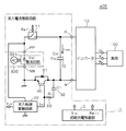
図17は、突入電流制限回路を備える別の従来の電力変換装置(以下、第2の従来技術と仮称する)の構成を示す回路図である。この電力変換装置452は、日本国公開特許公報:特開平8−289546号に開示された装置であり、スイッチ11aに代えて、トランジスタ30aおよびベース駆動回路11dが突入電流制限回路302に用いられている点において、第1の従来技術による電力変換装置451とは特徴的に異なっている。
【0009】
電力変換装置452においては、スイッチ11aに由来する問題点は解消されるものの、高い電力定格が要求される抵抗素子11bが必要である点に変わりはない。このため、電力変換装置452においても、重量および容積が大きく、製造コストも高いという問題点があった。また、高い電圧が印加された状態でスイッチ11が機械的な動作を行う必要がある点でも、電力変換装置451と変わりはなく、スイッチ11の信頼性および耐久性に問題点があった。
【0010】
図18は、突入電流制限回路を備えるさらに別の従来の電力変換装置(以下、第3の従来技術と仮称する)の構成を示す回路図である。この電力変換装置453は、スイッチ11aおよび抵抗素子11bに代えて、負温度係数サーミスタ(NTC;Negative Coefficient Thermistor)11cが突入電流制限回路303に用いられている点において、第1の従来技術による電力変換装置451とは特徴的に異なっている。
【0011】
通常において、インバータ13の始動時にはNTC11cの温度は低いため、高い抵抗を保持している。このため、スイッチ11がオンした後に流れる突入電流は、NTC11cの高抵抗によって制限される。NTC11cに発生する損失熱のために、NTC11cの温度は急速に上昇する。それにともない、NTC11cの抵抗は急速に低下するので、NTC11cによる損失は減少する。
【0012】
しかしながら、インバータ13が通常動作を行う間にNTC11cに発生する損失が、無視できない大きさであるであるため、電力変換装置453は電力定格の低い装置(例えば、数kW級以下の装置)としてのみ構成可能であるという問題点があった。また、例えばインバータ13を停止して間もなく再始動する場合など、NTC11cが十分に冷却されないときに、インバータ13を始動する場合には、NTC11cは、突入電流を制限する機能を十分に果たすことができず、信頼性および耐久性の上で問題点があった。
【0013】
(発明の開示)
本発明は、上記のような問題点を解決し、高い電力定格に対応可能で、装置の軽量化および縮小化を図りつつ、かつ高い信頼性および耐久性をもって突入電流を制限することのできる突入電流制限回路を得ることを目的とし、さらに当該突入電流制限回路を備えた電源装置および電力変換装置を提供することを目的とする。
【0014】
この目的を達成するために、この発明にかかる第1局面の装置は、突入電流制限回路であって、第1容量素子と、高電位用の一方主電極、低電位用の他方主電極及び制御電極を有し、前記第1容量素子の一端に前記一方主電極が接続された電荷駆動型の第1スイッチング素子と、前記第1スイッチング素子の前記一方主電極に一端が接続され、前記第1スイッチング素子の制御電極に他端が接続された第2容量素子と、を備える。
【0015】
この発明にかかる第2局面の装置は、第1局面の突入電流制限回路において、前記第1スイッチング素子の前記一方主電極と前記制御電極との間に介挿され、前記第2容量素子と直列に接続された第1抵抗素子を、さらに備える。
【0016】
この発明にかかる第3局面の装置は、第1局面の突入電流制限回路において、前記第1スイッチング素子に逆並列に接続された第1ダイオードを、さらに備える。
【0017】
この発明にかかる第4局面の装置は、第1局面の突入電流制限回路において、前記第1スイッチング素子の前記制御電極に接続され、前記第1スイッチング素子を制御信号にもとづいて駆動する駆動回路をさらに備える。
【0018】
この発明にかかる第5局面の装置では、第4局面の突入電流制限回路において、前記駆動回路が、前記第1スイッチング素子をオン駆動する駆動電流の経路に介挿された第1出力抵抗素子を備える。
【0019】
この発明にかかる第6局面の装置では、第4局面の突入電流制限回路において、前記駆動回路が、電源線に一方主電極が接続された第2スイッチング素子と、前記第2スイッチング素子の他方主電極に一端が接続され、前記第1スイッチング素子の前記制御電極に他端が接続された第1出力抵抗素子と、前記第1スイッチング素子の前記制御電極に一方主電極が接続され、前記第1スイッチング素子の他方主電極に他方主電極が接続され、前記第2スイッチング素子の制御電極に制御電極が接続された第3スイッチング素子と、を備える。
【0020】
この発明にかかる第7局面の装置では、第6局面の突入電流制限回路において、前記駆動回路が、前記第1スイッチング素子の前記制御電極と前記第3スイッチング素子の前記一方主電極との間に介挿された第2出力抵抗素子を、さらに備える。
【0021】
この発明にかかる第8局面の装置では、第4局面の突入電流制限回路において、前記駆動回路が、電源線に一方主電極が接続された第2スイッチング素子と、前記第2スイッチング素子の他方主電極に一方主電極が接続され、前記第1スイッチング素子の他方主電極に他方主電極が接続され、前記第2スイッチング素子の制御電極に制御電極が接続された第3スイッチング素子と、前記第2スイッチング素子と前記第3スイッチング素子との接続部に一端が接続され、前記第1スイッチング素子の前記制御電極に他端が接続された第1出力抵抗素子と、順電流が前記第1スイッチング素子をオフ駆動するように、前記第1出力抵抗素子に並列に接続された第2ダイオードと、を備える。
【0022】
この発明にかかる第9局面の装置では、第4局面の突入電流制限回路において、前記駆動回路が、電源線に一端が接続された第2抵抗素子と、前記第2抵抗素子の他端に一端が接続され、前記第1スイッチング素子の前記制御電極に他端が接続された第1出力抵抗素子と、前記第2抵抗素子の前記他端に一方主電極が接続され、前記第1スイッチング素子の他方主電極に他方主電極が接続された第3スイッチング素子と、順電流が前記第1スイッチング素子をオフ駆動するように、前記第1出力抵抗素子に並列に接続された第2ダイオードと、を備える。
【0023】
この発明にかかる第10局面の装置は、第1局面の突入電流制限回路において、前記第1容量素子および前記第1スイッチング素子へ直列に接続されたスイッチを、さらに備える。
【0024】
この発明にかかる第11局面の装置は、第10局面の突入電流制限回路において、始動指示にもとづいて、前記スイッチと前記第1スイッチング素子とをオンするように制御するとともに、停止指示にもとづいて、前記スイッチと前記第1スイッチング素子とをオフするように制御する初期充電制御部を、さらに備える。
【0025】
この発明にかかる第12局面の装置は、電源装置であって、第1容量素子と、高電位用の一方主電極、低電位用の他方主電極及び制御電極を有し、前記第1容量素子の一端に前記一方主電極が接続された電荷駆動型の第1スイッチング素子と、前記第1スイッチング素子の前記一方主電極に一端が接続され、前記第1スイッチング素子の制御電極に他端が接続された第2容量素子と、前記第1容量素子の他端に一端が接続され、前記第1スイッチング素子の他方主電極に他端が接続された直流電源と、前記第1容量素子、前記第1スイッチング素子および前記直流電源を環流する電流の経路に介挿されたスイッチと、を備える。
【0026】
この発明にかかる第13局面の装置は、電力変換装置において、第1容量素子と、前記第1容量素子の一端に一方主電極が接続された電荷駆動型の第1スイッチング素子と、前記第1スイッチング素子の前記一方主電極に一端が接続され、前記第1スイッチング素子の制御電極に他端が接続された第2容量素子と、前記第1容量素子の前記一端に一方主電極が接続された第4スイッチング素子と、前記第4スイッチング素子の他方主電極に一方主電極が接続され、前記第1容量素子の前記他端に他方主電極が接続された第5スイッチング素子と、前記第1容量素子の前記一端に一方主電極が接続された第6スイッチング素子と、前記第6スイッチング素子の他方主電極に一方主電極が接続され、前記第1容量素子の前記他端に他方主電極が接続された第7スイッチング素子と、を備える。
【0027】
この発明にかかる第14局面の装置は、第13局面の電力変換装置において、前記第4ないし第7スイッチング素子の通常動作を実現するために、これらを制御する制御部を、さらに備える。
【0028】
この発明にかかる第15局面の装置は、第14局面の電力変換装置において、前記第1容量素子および前記第1スイッチング素子へ直列に接続されたスイッチを、さらに備え、前記制御部は、始動指示にもとづいて、前記スイッチと前記第1スイッチング素子とをオンするように制御するとともに、停止指示にもとづいて、前記スイッチと前記第1スイッチング素子とをオフするように制御する。
【0029】
第1局面の装置は、第1容量素子の他端と第1スイッチング素子の他端とに直流電源が接続され、電力の供給を受ける様々な負荷が第1容量素子の一端と他端とに接続されることにより、使用に供される。負荷へ供給される電源電圧の変動が第1容量素子の働きにより抑えられ、第1容量素子への突入電流が、第1スイッチング素子と第2容量素子の働きにより抑えられる。
【0030】
しかも、第2容量素子のために第1スイッチング素子がオフからオンへと緩やかに遷移し、それによって突入電流が制限されるので、第1および第2の従来技術とは異なり、大電流が流れる電力用の抵抗素子が除去されるとともに、第3の従来技術とは異なり、電力定格を高く設定することが可能である。したがって、高い電力定格の下でも、装置の軽量化および縮小化を図ることができる。また、電力用の抵抗素子が除去されるので、電源電圧を供給するために外部のスイッチをオンするときに、当該スイッチに高電圧が印加されない。したがって、スイッチの信頼性および耐久性が損なわれない。
【0031】
第2局面の装置では、第1容量素子と第1スイッチング素子の制御電極との間に、第2容量素子に加えて第1抵抗素子が介挿されるので、第1スイッチング素子の発振が防止されるとともに、電源電圧を供給するために外部のスイッチをオンした直後に第1スイッチング素子が早々にオンすることを防止することができる。また、外部のスイッチをオンした直後に、第1容量素子および第2容量素子を通じて流れる初期充電電流が、第1抵抗素子によって効果的に制限される。
【0032】
第3局面の装置では、第1ダイオードが第1スイッチング素子に逆並列に接続されているので、第1スイッチング素子が逆電流から保護される。
【0033】
第4局面の装置では、第1スイッチング素子を駆動する駆動回路が備わるので、微小信号を制御信号として送出することにより、大電流定格の第1スイッチング素子を容易に駆動することができる。
【0034】
第5局面の装置では、第1スイッチング素子をオン駆動する駆動電流が、第1出力抵抗素子によって制限されるので、第1スイッチング素子のオフからオンへの遷移をさらに緩やかにすることができ、それにより突入電流をさらに効果的に制限することができる。
【0035】
第6局面の装置では、第1出力抵抗が備わるので、第1スイッチング素子のオフからオンへの遷移をさらに緩やかにすることができ、それにより突入電流をさらに効果的に制限することができる。また、第2スイッチング素子と第3スイッチング素子とが直列に接続され、一方のみがオンするので、リーク電流を抑制して駆動電力の消費を節減することができる。
【0036】
第7局面の装置では、第2出力抵抗素子が備わるので、第1スイッチング素子をオフ駆動する駆動電流を適切な大きさに設定することができる。
【0037】
第8局面の装置では、第1出力抵抗が備わるので、第1スイッチング素子のオフからオンへの遷移をさらに緩やかにすることができ、それにより突入電流をさらに効果的に制限することができる。また、第2スイッチング素子と第3スイッチング素子とが直列に接続され、一方のみがオンするので、リーク電流を抑制して駆動電力の消費を節減することができる。さらに、第2ダイオードが備わるので、第1スイッチング素子のオフからオンへの遷移に影響を与えることなく、オンからオフへの遷移を速めることができる。
【0038】
第9局面の装置では、第1出力抵抗素子および第2抵抗素子によって、第1スイッチング素子のオフからオンへの遷移をさらに緩やかにすることができ、それにより突入電流をさらに効果的に制限することができる。また、第1スイッチング素子のオン駆動とオフ駆動とが、単一のスイッチング素子によって行われるので、装置の簡素化および低コスト化が促進される。さらに、第2ダイオードが備わるので、第1スイッチング素子のオフからオンへの遷移に影響を与えることなく、オンからオフへの遷移を速めることができる。
【0039】
第10局面の装置では、スイッチが備わるので、外部にスイッチを設けることなく、電源電圧の供給を開始および停止することができる。また、第1および第2の従来技術とは異なり、大電流が流れる電力用の抵抗素子が除去されているので、スイッチをオンするときに、当該スイッチに高電圧が印加されない。したがって、スイッチの信頼性および耐久性が向上する。
【0040】
第11局面の装置では、初期充電制御部が備わるので、始動指示および停止指示を与えるだけで、スイッチと第1スイッチング素子とが自動的に動作する。
【0041】
第12局面の装置では、第1局面の装置が電流制限回路として備わるので、高い電力定格に対応可能で、装置の軽量化および縮小化を図りつつ、かつ高い信頼性および耐久性をもって突入電流を制限することができる電源装置が実現する。
【0042】
第13局面の装置では、第1局面の装置が電流制限回路として備わるので、高い電力定格に対応可能で、装置の軽量化および縮小化を図りつつ、かつ高い信頼性および耐久性をもって突入電流を制限する電力変換装置が実現する。
【0043】
第14局面の装置では、制御部が備わるので、通常動作のために、第4ないし第7スイッチング素子を制御する信号を外部から入力する必要がない。
【0044】
第15局面の装置では、制御部が始動指示および停止指示にもとづいてスイッチおよび第1スイッチング素子を制御するので、装置の操作が容易である。
【0045】
この発明の目的、特徴、局面、および利点は、以下の詳細な説明と添付図面とによって、より明白となる。
【0046】
(発明を実施するための最良の形態)
1. 実施の形態1
はじめに、本発明の実施の形態1による電力変換装置について説明する。
【0047】
1.1. 装置の構成の概略
図1は、本発明の実施の形態による電力変換装置の構成を示す回路図である。以下の図において、図16〜図18に示した従来技術による装置と同一部分または相当部分(同一の機能をもつ部分)については、同一符号を付して対応関係を明確にしている。
【0048】
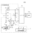
図1の電力変換装置401は、主電源10、突入電流制限回路1およびインバータ13を備えている。主電源10は、突入電流制限回路1の入力端子PP,NNに接続され、インバータ13は出力端子P,Nに接続されている。電力変換装置401は、インバータ5の出力端子U,V,Wに、例えばモータなどの三相の負荷100が接続されることにより、使用に供される。
【0049】
突入電流制限回路1は、スイッチ11、容量素子12、スイッチング素子30、ダイオード31、容量素子32、抵抗素子33、駆動回路20および初期充電制御部2を備えている。入力端子PP,NNには、直流の電源電圧VDC1が主電源10から供給される。容量素子12は、その容量CDCによって電源電圧VDC1を一定に保持する機能を果たす。スイッチ11は、リレーとして構成され、インバータ13を始動する際にオンし、停止する際にオフする主スイッチとして機能する。
【0050】
スイッチング素子30は、電荷駆動型(charge driven type)のスイッチング素子であり、実施の形態5を除いた以下の説明では、スイッチング素子30がIGBTである例を取り上げる。この場合には、スイッチング素子30の一対の主電極はコレクタおよびエミッタであり、制御電極はゲートである。スイッチング素子30のコレクタは容量素子12の一端に接続され、エミッタは入力端子NNに接続されている。
【0051】
このように、スイッチ11、容量素子12およびスイッチング素子30は、互いに直列に接続されており、これらが構成する直列回路の一端と他端が入力端子PPとNNに、それぞれ接続されている。一般には、直列回路の中で容量素子12およびスイッチング素子30が配置される順序は任意である。出力端子PおよびNは、容量素子12の一端と他端とに、それぞれ接続される。
【0052】
容量C1を有する容量素子32と抵抗R1を有する抵抗素子33は、互いに直列に接続されている。容量素子32と抵抗素子33とを有する直列回路の一端と他端は、スイッチング素子30のコレクタとゲートに、それぞれ接続されている。これにより、スイッチング素子30は、スイッチ11がオンした直後に容量素子12へ流れる突入電流を制限する機能を果たす。スイッチング素子30の動作の詳細については後述する。
【0053】
ダイオード31は、順電流が還流する方向にスイッチング素子30へ並列接続されている。本明細書では、ダイオードがスイッチング素子に、順電流が還流する方向に並列接続されることを、「逆並列に接続される」と表現する。ダイオード31は、スイッチング素子30を、逆電流から保護する機能を果たす。
【0054】
駆動回路20は、スイッチング素子30のゲートへ接続されており、制御信号VINにもとづいてゲート電圧VGをゲートへ伝達し、それによりスイッチング素子30を駆動する。駆動回路20は、例えば図2の回路図が示すように構成される。図2の駆動回路20は、スイッチング素子21,24、および出力抵抗素子22,23を備えている。
【0055】
スイッチング素子21,24の各々はMOSFETとして構成されており(ただし、バイポーラトランジスタも同様に使用可能である)、それらの一対の主電極はドレインおよびソースであり、制御電極はゲートである。P型のMOSFETであるスイッチング素子21のソースは、高電位電源線25に接続されている。出力抵抗素子22の一端は、スイッチング素子21のドレインに接続され、他端は信号線27を通じてスイッチング素子30のゲートに接続されている。
【0056】
N型のMOSFETであるスイッチング素子24のソースは、低電位電源線を通じて入力端子NNに接続されており、ゲートはスイッチング素子21のゲートに接続されている。二つのスイッチング素子21,24のゲートには、信号線26を通じて制御信号VINが入力される。出力抵抗素子23の一端は、スイッチング素子24のドレインに接続され、他端は信号線27を通じてスイッチング素子30のゲートに接続されている。
【0057】
二つのスイッチング素子21,24は、制御信号VINにもとづいて排他的にオンする。スイッチング素子21はオンすることにより、スイッチング素子30をオン駆動する駆動電流を出力する。出力抵抗素子22の抵抗RGONは、スイッチング素子30をオン駆動するときの出力抵抗として機能する。スイッチング素子24はオンすることにより、スイッチング素子30をオフ駆動する駆動電流を吸い込む。出力抵抗素子23の抵抗RGOFFは、スイッチング素子30をオフ駆動するときの出力抵抗として機能する。
【0058】
抵抗RGOFFは、スイッチング素子30のオンからオフへの遷移を速めるために、また、スイッチング素子30が不用意にオンすることを防ぐために、数Ωないしそれ以下の低い値に設定される。これとは逆に、抵抗RGONは、スイッチング素子30のオフからオンへの遷移を緩やかにし、それにより容量素子12へ流れる突入電流を制限するために、高い値に設定される。
【0059】
図1に戻って、初期充電制御部2は、制御信号Rel1をスイッチ11へ伝達し、制御信号VINを駆動回路20へ伝達することにより、スイッチ11およびスイッチング素子30を制御する。初期充電制御部2は、外部から始動指示が入力されると、スイッチ11とスイッチング素子30とをオンするように制御する。また、初期充電制御部2は、外部から停止指示が入力されると、スイッチ11とスイッチング素子30とをオフするように制御する。始動指示および停止指示は、例えば操作者が図示しないスイッチを操作することによって入力される。
【0060】
なお、主電源10と突入電流制限回路1とを組み合わせることにより、突入電流を制限する機能を有する電源装置を構成することができる。
【0061】
1.2. 装置の動作
つぎに、電力変換装置401の動作について説明する。スイッチ11がオンした直後に容量素子12を流れる突入電流を制限する特徴的な動作の原理は、スイッチング素子30がオフからオンへ遷移する過程を考慮することによって説明することができる。
【0062】
スイッチング素子30は、電荷駆動型(charge driven type)、すなわち電圧制御型(voltage controlled type)である。すなわち、スイッチング素子30は、オンするときには等価的な入力容量が充電されることにより制御され、オフするときには入力容量が放電されることにより制御される。
【0063】
図3は、スイッチング素子30の等価回路を単純化して示す回路図である。図3は、スイッチング素子30がIGBTである例を示しているが、MOSFETであっても同様である。スイッチング素子30には、ゲート−エミッタ容量CGE、ゲート−コレクタ容量CGC(逆伝達容量{reverse transfer capacitance}またはミラー容量{Miller capacitance}とも称される)、およびコレクタ−エミッタ容量CCEが等価的に含まれている。
【0064】
図4は、図1に示した容量素子32および抵抗素子33が存在しない場合に、スイッチング素子30がオフからオンへ遷移する過程にともなう突入電流制限回路1の各部の電圧および電流の変化を示すタイミングチャートである。スイッチング素子30がオフから完全なオンへと遷移するためには、ゲート−コレクタ容量CGCおよびコレクタ−エミッタ容量CCEで構成される入力容量が、駆動回路20によって充電されなければならない。
【0065】
スイッチング素子30をオンするために、駆動回路20のスイッチング素子21がオンしスイッチング素子24がオフすると(時刻=0)、抵抗RGONを通じて流れる駆動電流によりゲート−エミッタ容量CGEの充電が開始される。ゲート−エミッタ容量CGEが充電されることにより、ゲート−エミッタ間電圧VGEが閾値電圧Vthに達すると、スイッチング素子30にはコレクタ電流(容量素子12を流れる充電電流ICHGに一致する)が流れ始める。しかしながら、コレクタ−エミッタ間電圧VCEは、オフ状態に対応する高い値(すなわち、主電源10の電源電圧VDC1)を維持する。
【0066】
ゲート−エミッタ容量CGEの充電は、時刻T1まで定常的に継続する。時刻T1では、ゲート−コレクタ容量CGCの充電が開始され、その結果、ゲート−エミッタ間電圧VGEは一定の電圧(すなわち、ミラー電圧{Miller voltage})Vmにとどまる。コレクタ電流ICHGは、ゲート−エミッタ間電圧VGEの上昇にともなって増加し、時刻T1でその最大値I chg1 に達する。
【0067】
時刻T1の後に、コレクタ−エミッタ間電圧VCEが急激な下降を開始する。これにともない、ゲート−コレクタ容量CGCは、より多くの充電電流が供給されることを必要とする(ミラー効果{Miller effect})。これが、ゲート−エミッタ間電圧VGEが期間T1〜T2において、略一定の電圧Vmを維持する原因となっている。コレクタ−エミッタ間電圧VCEの変化が緩やかになると、ゲート−エミッタ間電圧VGEは再び上昇を開始する。時刻T3において、ゲート−エミッタ間電圧VGEが、その最高値(すなわち、駆動回路20の電源電圧VCC)に達すると、コレクタ−エミッタ間電圧VCEは、その最低値であるオン状態での値(すなわち、コレクタ−エミッタ間飽和電圧V)CE(sat)に達する。
【0068】
図1が示すように、スイッチング素子30は、主電源10と容量素子12との間に直列に接続されているので、容量素子12の充電電圧VDC(図4の(B))の波形は、コレクタ−エミッタ間電圧VCE(図4の(C))の波形を逆転したものと一致する。このように、容量素子12の充電電圧VDCの変化率(すなわち、dVDC/dt)は、期間T1〜T2におけるスイッチング素子30の遷移過程によって規定される。
【0069】
図4の(A)が示すように、充電電圧VDCの変化率は、主電源10から容量素子12を通過して流れる充電電流ICHG(すなわち突入電流)を規定する。したがって、期間T1〜T2において、スイッチング素子30がオフからオンへ遷移する過程を制御することによって、充電電流ICHGを制御することが可能となる。すなわち、期間T1〜T2における容量素子12の充電電圧VDCの変化率を引き下げること、言い換えると、期間T1〜T2を長くすることによって、突入電流を減少させることができる。このことは、図5の回路図が示すように、スイッチング素子30の外部に、容量素子32を付加することによって達成される。容量素子32の容量C1は、付加的なゲート−コレクタ容量として機能する。
【0070】
図6は、図5が示すように容量素子32および抵抗素子33がスイッチング素子30に接続されている場合に、スイッチング素子30がオフからオンへ遷移する過程にともなう突入電流制限回路1の各部の電圧および電流の変化を示すタイミングチャートである。外部の容量素子32を充電するのに余分な時間を要するために、期間T1a〜T2aにおける充電電圧VDCの変化率が減少することが理解される。期間T1a〜T2aにおける充電電圧VDCの変化率の減少は、容量素子12を流れる突入電流(すなわち、充電電流ICHG)の減少をもたらしている。
【0071】
つぎに、電力変換装置401の動作の流れについて説明する。初期においては、スイッチ11はオフに保たれ、スイッチング素子30もオフに保たれている。スイッチング素子21がオフし、スイッチング素子24がオンすることにより、スイッチング素子30はオフに保たれている。初期充電制御部2の制御によりスイッチ11がオンすると、初期充電電流が、主電源10からスイッチ11、容量素子12、容量素子32、抵抗素子33、抵抗素子23、およびスイッチング素子24を流れる。この初期充電電流は、主として抵抗素子33によって制限されている。なぜなら上記したように、抵抗素子23の抵抗RGOFFは、数Ωないしそれ以下の低い値に設定されているからである。
【0072】
つぎに、初期充電制御部2は、スイッチング素子30をオンするように制御信号VINを駆動回路20へ伝達する。その結果、図6に示した動作が実現する。容量素子12が十分に充電され、充電電圧VDCが電源電圧VDC1に達すると、インバータ13が通常動作を開始する。インバータ13が動作を停止すると、初期充電制御部2はスイッチ11およびスイッチング素子30をオフする。
【0073】
1.3. 実証データ
つぎに、電力変換装置401の性能を実証するために行われたコンピュータシミュレーションについて説明する。シミュレーションの対象とされた電力変換装置401では、駆動回路20は図2のように構成された。各種のパラメータは、以下のように設定された。
【0074】
VDC1=300V;Vcc=15V;RGON=10kΩ;RGOFF=1Ω;R1=100Ω;C1=10nFおよび100nF(2通り);CDC=1.2mF;容量素子12の実効直列抵抗ESR=1mΩ;容量素子12の実効直列誘導ESL=20nH;スイッチング素子30=IGBT(定格300A/600V)。
【0075】
図7は、C1=10nFであるときのシミュレーションの結果を示すグラフである。また、図8は、C1=100nFであるときのシミュレーションの結果を示すグラフである。
【0076】
C1=10nFであるときには、スイッチング素子30をオンすべく制御信号VINが駆動回路20へ伝達された(時刻=0)後に、時刻が約5msecを経た時点で充電電圧VDCが電源電圧VDC1に達しているのに対し、C1=100nFであるときには、時刻が約38msecを経た時点で充電電圧VDCが電源電圧VDC1に達している。それにともない、充電電流ICHGの最大値は、C1=10nFであるときには約70Aであるのに対し、C1=100nFであるときには約10Aに抑えられている。
【0077】
このように、シミュレーションの結果は、容量素子32の容量C1を大きく設定することにより、容量素子12を流れる突入電流を減少させることができることを明瞭に示している。すなわち、シミュレーションの結果は、電力変換装置401が期待通りに動作することを実証している。
【0078】
1.4. 装置の利点
以上に述べたように、電力変換装置401では、容量素子12を流れる突入電流が、スイッチング素子30と容量素子32の働きにより抑えられる。しかも、容量素子32のためにスイッチング素子30がオフからオンへと緩やかに遷移し、それによって突入電流が制限されるので、第1および第2の従来技術とは異なり、大電流が流れる電力用の抵抗素子11bが除去されるとともに、第3の従来技術とは異なり、電力定格を高く設定することが可能である。したがって、高い電力定格の下でも、装置の軽量化および縮小化を図ることができる。また電力用の抵抗素子11bが除去されるので、スイッチ11をオンするときに、スイッチ11に高電圧が印加されない。したがって、スイッチ11の信頼性および耐久性が向上する。
【0079】
また、容量素子32に直列に抵抗素子33が接続されるので、スイッチング素子30のゲートにおける発振が防止されるとともに、スイッチ11をオンした直後にスイッチング素子30が早々にオンすることを防止することができる。また、スイッチ11がオンした直後に、容量素子12および容量素子32を通じて流れる初期充電電流が、抵抗素子33によって効果的に制限される。
【0080】
また、スイッチング素子30をオン駆動する駆動電流が、出力抵抗素子22の抵抗RGONによって制限される。したがって、スイッチング素子30のオフからオンへの遷移をさらに緩やかにすることができ、それにより突入電流をさらに効果的に制限することができる。さらに、スイッチング素子21とスイッチング素子24とが直列に接続され、双方は互いに排他的にオンするので、リーク電流を抑制して駆動電力の消費を節減することができる。
【0081】
2. 実施の形態2
図9は、実施の形態2による駆動回路20の構成を示す回路図である。この駆動回路20は、スイッチング素子24のドレインとスイッチング素子30のゲートとが、抵抗素子を介することなく信号線27で接続されている点において、実施の形態1の駆動回路20とは、特徴的に異なっている。実施の形態1の駆動回路20から抵抗素子23が除去されているので、装置の構成がより簡素であるという利点がある。また、スイッチング素子30をオフ駆動する電流が抵抗素子23によって制限されないので、スイッチング素子30のオンからオフへの遷移を速めることができる。
【0082】
3. 実施の形態3
図10は、実施の形態3による駆動回路20の構成を示す回路図である。この駆動回路20は、スイッチング素子21のドレインとスイッチング素子24のドレインとが接続されており、その接続部とスイッチング素子30のゲートとの間に、抵抗素子22とダイオード29とが並列に接続されて成る並列回路が介挿されている点において、実施の形態1の駆動回路20とは、特徴的に異なっている。ダイオード29の向きは、順電流がスイッチング素子30をオフ駆動する駆動電流となるように設定されている。
【0083】
図10の駆動回路20においても、図2の駆動回路20と同様に、スイッチング素子30をオン駆動する駆動電流は、ダイオード29の干渉を受けることなく、出力抵抗素子22によって制限される。一方、スイッチング素子30をオフ駆動する駆動電流は、ダイオード29を流れる。このため、図9の駆動回路20と同様に、スイッチング素子30のオンからオフへの遷移を速めることができる。
【0084】
4. 実施の形態4
図11は、実施の形態4による駆動回路20の構成を示す回路図である。この駆動回路20は、スイッチング素子21が抵抗素子28に置き換えられている点において、実施の形態3の駆動回路20とは、特徴的に異なっている。スイッチング素子30をオン駆動する駆動電流は、ダイオード29の干渉を受けることなく、出力抵抗素子22の抵抗RGONおよび抵抗素子28の抵抗RDの合成抵抗によって制限される。また、スイッチング素子30をオフ駆動する駆動電流は、ダイオード29を流れる。このため、図10の駆動回路20と同様に、スイッチング素子30のオンからオフへの遷移を速めることができる。また、スイッチング素子21が抵抗素子28に置き換えられているので、装置の構成がより簡素である。ただし、図2、図9および図10が示す駆動回路20では、高電位電源線25から低電位電源線へ流れるリーク電流が抑えられるので、駆動電力の消費が低いという利点がある。
【0085】
5. 実施の形態5
図12は、実施の形態5の電力変換装置の構成を示す回路図である。この電力変換装置402は、スイッチング素子30としてMOSFET40が用いられている点において、実施の形態1の電力変換装置401とは特徴的に異なっている。スイッチング素子30として、電荷駆動型のスイッチング素子が一般に利用可能である。電力変換装置401におけるIGBT、および電力変換装置402におけるMOSFETは、広く用いられており、様々な定格のものが入手可能であるという利点がある。
【0086】
6. 実施の形態6
図13は、実施の形態6の電力変換装置の構成を示す回路図である。この電力変換装置403は、スイッチング素子30およびダイオード31が、入力端子PPと出力端子Pとを接続する高電位電源線に介挿されている点において、実施の形態1の電力変換装置401とは特徴的に異なっている。実施の形態1において既述したように、一般に、スイッチ11、スイッチング素子30および容量素子12は、互いに直列に接続され、出力端子PPおよびNNが容量素子12の一端と他端とに接続されておればよい。図13は、この一般的な形態の範囲内で、図1とは異なる一例を示すものである。
【0087】
7. 実施の形態7
図14は、実施の形態7の電力変換装置の構成を示す回路図である。この電力変換装置404は、インバータ13に統合制御部201が備わっている点において、実施の形態1の電力変換装置401とは特徴的に異なっている。統合制御部201は、インバータ13に備わる一群のスイッチング素子51,54,61,64,71,74の通常動作を実現するために、これらを制御する主制御部としての機能と、突入電流制限回路1に備わるスイッチ11およびスイッチング素子30を制御する初期充電制御部2としての機能との双方を同時に果たしている。
【0088】
統合制御部201は、CPU203とメモリ204とを備えている。CPU203はメモリ204に格納されるプログラムにしたがって動作することによって、一群のスイッチング素子51,54,61,64,71,74の通常動作を実現し、かつスイッチ11およびスイッチング素子30を制御する。
【0089】
スイッチング素子51,54,61,64,71,74の各々は、一般には、制御電極へ入力される信号に応答して、一対の主電極を通じて流れる主電流の大きさを制御する半導体素子であるが、好ましくは、パワーIGBT、パワーバイポーラトランジスタ、および、パワーMOSFETなどのパワー(電力用)スイッチング素子である。中でも、パワーIGBTは、導通(オン)状態での一対の主電極間の電圧である飽和電圧VCE(sat)が低く、しかも、制御が容易な電圧制御型であるという利点を有している。このため、以下の説明では、スイッチング素子51,54,61,64,71,74の各々が、パワーIGBTである例を取り上げる。
【0090】
スイッチング素子51,61,71のコレクタは、突入電流制限回路1の出力端子Pに接続されている。また、スイッチング素子54,64,74のコレクタは、それぞれスイッチング素子51,61,71のエミッタに接続され、エミッタは突入電流制限回路1の出力端子Nに接続されている。インバータ13の出力端子Uは、スイッチング素子51と54の接続部に接続され、出力端子Vはスイッチング素子61と64の接続部に接続され、出力端子Wは、スイッチング素子71と74の接続部に接続されている。
【0091】
インバータ13は、さらに、フリーホイールダイオード52,55,62,65,72,75、および駆動回路50,53,60,63,70,73を備えている。フリーホイールダイオード52,55,62,65,72,75は、スイッチング素子51,54,61,64,71,74に、逆並列に接続されている。フリーホイールダイオード52,55,62,65,72,75は、それぞれスイッチング素子51,54,61,64,71,74を、逆電流から保護するために設けられている。
【0092】
駆動回路50,53,60,63,70,73は、それぞれスイッチング素子51,54,61,64,71,74のゲートに接続されている。駆動回路50,53,60,63,70,73は、それぞれ統合制御部201が出力する制御信号UP,UN,VP,VN,W,PWNに応答して、それぞれスイッチング素子51,54,61,64,71,74を駆動する。
【0093】
統合制御部201を、制御信号UP,UN,VP,VN,WP,WNを出力することによりスイッチング素子51,54,61,64,71,74の通常動作を実現する主制御部と、スイッチ11およびスイッチング素子30を制御する初期充電制御部2とに分離することも可能である。このとき、初期充電制御部2は、始動指示および停止指示を、主制御部から受信することも可能である。ただし、主制御部と初期充電制御部2とを単一の統合制御部201へ統合した図14の形態では、装置が全体として簡素かつ軽量に構成されるとともに、製造コストが節減されるという利点が得られる。
【0094】
8. 実施の形態8
図15は、実施の形態8の電力変換装置の構成を示す回路図である。この電力変換装置405は、外部の交流電源300から入力される交流電圧を直流の電源電圧VDC1へ変換する整流回路301を備える点において、実施の形態1の電力変換装置401とは特徴的に異なっている。整流回路301は、電源電圧VDC1を、入力端子PPと入力端子NNとの間に印加する。したがって、電力変換装置405は、外部に電力用の直流電源を準備することなく、入手し易い交流電源300を接続するだけで、使用に供することができる。
【0095】
この発明は詳細に説明されたが、上記した説明は、すべての局面において、例示であって、この発明がそれに限定されるものではない。例示されていない無数の変形例が、この発明の範囲から外れることなく想定され得るものと解される。
【図面の簡単な説明】
【図1】 実施の形態1による電力変換装置の構成を示す回路図である。
【図2】 図1の駆動回路の構成を示す回路図である。
【図3】 スイッチング素子30の等価回路図である。
【図4】 図1の電力変換装置に対比される装置の動作を示すタイミングチャートである。
【図5】 スイッチング素子30の等価回路図である。
【図6】 図1の電力変換装置の動作を示すタイミングチャートである。
【図7】 図1の電力変換装置に関するシミュレーションの結果を示すグラフである。
【図8】 図1の電力変換装置に関するシミュレーションの結果を示すグラフである。
【図9】 実施の形態2による駆動回路の構成を示す回路図である。
【図10】 実施の形態3による駆動回路の構成を示す回路図である。
【図11】 実施の形態4による駆動回路の構成を示す回路図である。
【図12】 実施の形態5による電力変換装置の構成を示す回路図である。
【図13】 実施の形態6による電力変換装置の構成を示す回路図である。
【図14】 実施の形態7による電力変換装置の構成を示す回路図である。
【図15】 実施の形態8による電力変換装置の構成を示す回路図である。
【図16】 第1の従来技術による電力変換装置の構成を示す回路図である。
【図17】 第2の従来技術による電力変換装置の構成を示す回路図である。
【図18】 第3の従来技術による電力変換装置の構成を示す回路図である。[0001]
(Technical field)
The present invention relates to an inrush current limiting circuit, a power supply device, and a power conversion device, and in particular, can cope with a high power rating, reduce the weight and size of the device, and achieve an inrush current with high reliability and durability. It relates to improvements to limit.
[0002]
(Background technology)
FIG. 16 is a circuit diagram showing a configuration of a conventional power conversion device (hereinafter referred to as first conventional technology) including an inrush current limiting circuit. The
[0003]
The inrush current limiting
[0004]
The
[0005]
The charging voltage of the
[0006]
However, since a large current supplied from the
[0007]
Further, the
[0008]
FIG. 17 is a circuit diagram showing a configuration of another conventional power conversion device (hereinafter, tentatively referred to as second conventional technology) including an inrush current limiting circuit. This
[0009]
In the
[0010]
FIG. 18 is a circuit diagram showing a configuration of still another conventional power conversion device (hereinafter referred to as third conventional technology) having an inrush current limiting circuit. This
[0011]
Normally, when the
[0012]
However, since the loss generated in the NTC 11c during the normal operation of the
[0013]
(Disclosure of the Invention)
The present invention solves the above-mentioned problems, can cope with high power ratings, can reduce the size and weight of the device, and can limit the inrush current with high reliability and durability. It aims at obtaining a current limiting circuit, and also aims at providing the power supply device and power converter device provided with the said inrush current limiting circuit.
[0014]
In order to achieve this object, an apparatus according to a first aspect of the present invention is an inrush current limiting circuit, comprising: a first capacitive element;One main electrode for high potential, the other main electrode for low potential and a control electrode,At one end of the first capacitive elementAboveOne charge-driven first switching element connected to the main electrode, and one end connected to the one main electrode of the first switching element and the other end connected to the control electrode of the first switching element A capacitive element.
[0015]
The device according to a second aspect of the present invention is the inrush current limiting circuit according to the first aspect, wherein the device is interposed between the one main electrode of the first switching element and the control electrode, and is in series with the second capacitive element. The 1st resistance element connected to is further provided.
[0016]
The device according to a third aspect of the present invention further includes a first diode connected in antiparallel to the first switching element in the inrush current limiting circuit according to the first aspect.
[0017]
According to a fourth aspect of the present invention, there is provided a drive circuit that is connected to the control electrode of the first switching element and drives the first switching element based on a control signal in the inrush current limiting circuit of the first aspect. Further prepare.
[0018]
In the device according to the fifth aspect of the present invention, in the inrush current limiting circuit according to the fourth aspect, the drive circuit includes a first output resistance element inserted in a path of a drive current that drives the first switching element on. Prepare.
[0019]
In the device according to the sixth aspect of the present invention, in the inrush current limiting circuit according to the fourth aspect, the drive circuit includes a second switching element having one main electrode connected to a power line, and the other main element of the second switching element. One main electrode is connected to the first output resistance element having one end connected to the electrode, the other end connected to the control electrode of the first switching element, and the control electrode of the first switching element;The other main electrode is connected to the other main electrode of the first switching element;A third switching element having a control electrode connected to the control electrode of the second switching element.
[0020]
In the device according to the seventh aspect of the present invention, in the inrush current limiting circuit according to the sixth aspect, the drive circuit is provided between the control electrode of the first switching element and the one main electrode of the third switching element. An intervening second output resistance element is further provided.
[0021]
In the apparatus according to the eighth aspect of the present invention, in the inrush current limiting circuit according to the fourth aspect, the drive circuit includes a second switching element having one main electrode connected to a power line, and the other main element of the second switching element. A third switching element having one main electrode connected to the electrode, the other main electrode connected to the other main electrode of the first switching element, and a control electrode connected to the control electrode of the second switching element; A first output resistance element having one end connected to a connection portion between the switching element and the third switching element and the other end connected to the control electrode of the first switching element; and a forward current passing through the first switching element. A second diode connected in parallel to the first output resistance element so as to be driven off.
[0022]
In the device according to the ninth aspect of the present invention, in the inrush current limiting circuit according to the fourth aspect, the drive circuit includes a second resistance element having one end connected to a power supply line, and one end at the other end of the second resistance element. And a first output resistor element having the other end connected to the control electrode of the first switching element, and one main electrode connected to the other end of the second resistor element, A third switching element having the other main electrode connected to the other main electrode, and a second diode connected in parallel to the first output resistance element such that a forward current drives the first switching element off. Prepare.
[0023]
The device according to a tenth aspect of the present invention is the inrush current limiting circuit according to the first aspect, further comprising a switch connected in series to the first capacitive element and the first switching element.
[0024]
According to an eleventh aspect of the present invention, in the inrush current limiting circuit of the tenth aspect, the device controls the switch and the first switching element to turn on based on a start instruction, and based on a stop instruction. And an initial charge control unit for controlling the switch and the first switching element to be turned off.
[0025]
A device according to a twelfth aspect of the present invention is a power supply device, comprising: a first capacitive element;One main electrode for high potential, the other main electrode for low potential and a control electrode,At one end of the first capacitive elementAboveOne charge-driven first switching element connected to the main electrode, and one end connected to the one main electrode of the first switching element and the other end connected to the control electrode of the first switching element A capacitive element; a DC power source having one end connected to the other end of the first capacitive element and the other end connected to the other main electrode of the first switching element; the first capacitive element; the first switching element; And a switch interposed in a current path circulating in the DC power source.
[0026]
According to a thirteenth aspect of the present invention, in the power converter, the first capacitive element, the charge-driven first switching element having one main electrode connected to one end of the first capacitive element, and the first One end of the switching element is connected to the one main electrode, the other end of the first switching element is connected to the control electrode, and the other end of the first capacity element is connected to the one main electrode. A fourth switching element; a fifth switching element having one main electrode connected to the other main electrode of the fourth switching element; and the other main electrode connected to the other end of the first capacitor; and the first capacitor A sixth switching element having one main electrode connected to the one end of the element; a main electrode connected to the other main electrode of the sixth switching element; and the other main electrode connected to the other end of the first capacitive element. Comprising a seventh switching element, the.
[0027]
A device according to a fourteenth aspect of the present invention is the power conversion device according to the thirteenth aspect, further comprising a control unit for controlling the fourth to seventh switching elements in order to realize normal operation.
[0028]
A device according to a fifteenth aspect of the present invention is the power conversion device according to the fourteenth aspect, further comprising a switch connected in series to the first capacitive element and the first switching element, wherein the control unit includes a start instruction. Based on the control, the switch and the first switching element are controlled to be turned on, and the switch and the first switching element are controlled to be turned off based on a stop instruction.
[0029]
In the apparatus of the first aspect, a DC power source is connected to the other end of the first capacitive element and the other end of the first switching element, and various loads receiving power supply are connected to the one end and the other end of the first capacitive element. By being connected, it is used. The fluctuation of the power supply voltage supplied to the load is suppressed by the function of the first capacitor element, and the inrush current to the first capacitor element is suppressed by the functions of the first switching element and the second capacitor element.
[0030]
In addition, since the first switching element gradually changes from OFF to ON due to the second capacitor element, and the inrush current is limited thereby, a large current flows unlike the first and second conventional techniques. Unlike the third prior art, the power rating can be set high while the power resistance element is removed. Therefore, it is possible to reduce the weight and size of the device even under a high power rating. Further, since the power resistive element is removed, when the external switch is turned on to supply the power supply voltage, a high voltage is not applied to the switch. Therefore, the reliability and durability of the switch are not impaired.
[0031]
In the device of the second aspect, since the first resistance element is inserted in addition to the second capacitance element between the first capacitance element and the control electrode of the first switching element, oscillation of the first switching element is prevented. In addition, it is possible to prevent the first switching element from being turned on immediately after the external switch is turned on to supply the power supply voltage. Further, immediately after the external switch is turned on, the initial charging current flowing through the first capacitor element and the second capacitor element is effectively limited by the first resistor element.
[0032]
In the device according to the third aspect, since the first diode is connected in antiparallel to the first switching element, the first switching element is protected from the reverse current.
[0033]
Since the device according to the fourth aspect includes a drive circuit that drives the first switching element, the first switching element with a large current rating can be easily driven by sending a minute signal as a control signal.
[0034]
In the device of the fifth aspect, since the drive current for driving the first switching element on is limited by the first output resistance element, the transition of the first switching element from OFF to ON can be made more gradual, Thereby, the inrush current can be more effectively limited.
[0035]
In the device according to the sixth aspect, since the first output resistor is provided, the transition from the OFF state to the ON state of the first switching element can be further moderated, and thereby the inrush current can be more effectively limited. In addition, since the second switching element and the third switching element are connected in series and only one of them is turned on, the leakage current can be suppressed and consumption of driving power can be reduced.
[0036]
In the device according to the seventh aspect, since the second output resistance element is provided, the drive current for driving the first switching element off can be set to an appropriate magnitude.
[0037]
In the device according to the eighth aspect, since the first output resistance is provided, the transition from the OFF state to the ON state of the first switching element can be further moderated, and thereby the inrush current can be more effectively limited. In addition, since the second switching element and the third switching element are connected in series and only one of them is turned on, the leakage current can be suppressed and consumption of driving power can be reduced. Furthermore, since the second diode is provided, the transition from on to off can be accelerated without affecting the transition from off to on of the first switching element.
[0038]
In the device according to the ninth aspect, the first output resistive element and the second resistive element can further moderate the transition from the OFF state to the ON state of the first switching element, thereby further effectively limiting the inrush current. be able to. Further, since the first switching element is turned on and off by a single switching element, simplification and cost reduction of the device are promoted. Furthermore, since the second diode is provided, the transition from on to off can be accelerated without affecting the transition from off to on of the first switching element.
[0039]
In the device according to the tenth aspect, since the switch is provided, the supply of the power supply voltage can be started and stopped without providing an external switch. Further, unlike the first and second prior arts, since the power resistive element through which a large current flows is removed, a high voltage is not applied to the switch when the switch is turned on. Therefore, the reliability and durability of the switch are improved.
[0040]
In the apparatus of the eleventh aspect, since the initial charge control unit is provided, the switch and the first switching element automatically operate only by giving a start instruction and a stop instruction.
[0041]
In the device of the twelfth aspect, since the device of the first aspect is provided as a current limiting circuit, the inrush current can be handled with high reliability and durability while being able to cope with a high power rating and reducing the weight and size of the device. A power supply that can be limited is realized.
[0042]
In the device of the thirteenth aspect, since the device of the first aspect is provided as a current limiting circuit, the inrush current can be handled with high reliability and durability while being able to cope with a high power rating, reducing the weight and size of the device. The power conversion device to be limited is realized.
[0043]
In the device of the fourteenth aspect, since the control unit is provided, it is not necessary to input a signal for controlling the fourth to seventh switching elements from the outside for normal operation.
[0044]
In the device according to the fifteenth aspect, since the control unit controls the switch and the first switching element based on the start instruction and the stop instruction, the operation of the apparatus is easy.
[0045]
The objects, features, aspects and advantages of the present invention will become more apparent from the following detailed description and the accompanying drawings.
[0046]
(Best Mode for Carrying Out the Invention)
1.
First, the power conversion device according to
[0047]
1.1. Outline of device configuration
FIG. 1 is a circuit diagram showing a configuration of a power conversion device according to an embodiment of the present invention. In the following drawings, the same or corresponding parts (parts having the same function) as those of the prior art apparatus shown in FIGS. 16 to 18 are assigned the same reference numerals to clarify the correspondence.
[0048]
A
[0049]
The inrush current limiting
[0050]
The switching
[0051]
In this way, the
[0052]
Capacity C1Capacitor 32 having a resistance R1Resistive elements 33 having are connected to each other in series. One end and the other end of the series circuit including the
[0053]
The
[0054]
The
[0055]
Each of the switching
[0056]
The source of the switching
[0057]
The two
[0058]
Resistance RGOFFIs set to a low value of several Ω or less in order to speed up the transition from on to off of the switching
[0059]
Returning to FIG. 1, the initial
[0060]
In addition, by combining the
[0061]
1.2. Operation of the device
Next, the operation of the
[0062]
The switching
[0063]
FIG. 3 is a circuit diagram showing a simplified equivalent circuit of the switching
[0064]
FIG. 4 shows changes in voltage and current in each part of the inrush current limiting
[0065]
In order to turn on the switching
[0066]
Gate-emitter capacitance CGEThe charging continues continuously until time T1. At time T1, gate-collector capacitance CGCAs a result, the gate-emitter voltage VGERemains at a constant voltage (ie, Miller voltage) Vm. Collector current ICHGIs the gate-emitter voltage VGEIncreases as time rises and reaches its maximum at time T1I chg1 To reach.
[0067]
After time T1, the collector-emitter voltage VCEBegins to drop sharply. Accordingly, gate-collector capacitance CGCRequires more charging current to be supplied (Miller effect). This is the gate-emitter voltage VGEHowever, this is a cause of maintaining a substantially constant voltage Vm in the period T1 to T2. Collector-emitter voltage VCEWhen the change in voltage becomes slow, the gate-emitter voltage VGEStarts rising again. At time T3, the gate-emitter voltage VGEIs the maximum value (that is, the power supply voltage V of the drive circuit 20).CC), The collector-emitter voltage VCEIs the lowest value in the on state (ie, collector-emitter saturation voltage V)CE (sat)To reach.
[0068]
As shown in FIG. 1, since the switching
[0069]
As shown in FIG. 4A, the charging voltage VDCOf the charging current I flowing from the
[0070]
FIG. 6 shows each part of the inrush current limiting
[0071]
Next, the operation flow of the
[0072]
Next, the initial
[0073]
1.3. Demonstration data
Next, a computer simulation performed to verify the performance of the
[0074]
VDC1= 300V; Vcc= 15V; RGON= 10kΩ; RGOFF= 1Ω; R1= 100Ω; C1= 10 nF and 100 nF (2 ways); CDC= 1.2 mF; Effective series resistance ESR of
[0075]
FIG. 7 shows C1It is a graph which shows the result of simulation when it is = 10 nF. In addition, FIG.1It is a graph which shows the result of a simulation when it is = 100nF.
[0076]
C1= 10 nF, the control signal V to turn on the switching
[0077]
Thus, the result of the simulation is the capacitance C of the capacitive element 32.1It is clearly shown that the inrush current flowing through the
[0078]
1.4. Equipment advantages
As described above, in the
[0079]
In addition, since the
[0080]
In addition, the drive current for driving the switching
[0081]
2.
FIG. 9 is a circuit diagram showing a configuration of the
[0082]
3.
FIG. 10 is a circuit diagram showing a configuration of the
[0083]
Also in the
[0084]
4.
FIG. 11 is a circuit diagram showing a configuration of the
[0085]
5.
FIG. 12 is a circuit diagram showing a configuration of the power conversion device according to the fifth embodiment. The
[0086]
6. Embodiment 6
FIG. 13 is a circuit diagram showing a configuration of the power conversion device according to the sixth embodiment. This
[0087]
7. Embodiment 7
FIG. 14 is a circuit diagram showing a configuration of the power conversion device according to the seventh embodiment. This
[0088]
The
[0089]
Each of switching
[0090]
The collectors of the switching
[0091]
The
[0092]
The
[0093]
The
[0094]
8.
FIG. 15 is a circuit diagram showing a configuration of the power conversion device according to the eighth embodiment. This
[0095]
Although the present invention has been described in detail, the above description is illustrative in all aspects, and the present invention is not limited thereto. It is understood that countless variations that are not illustrated can be envisaged without departing from the scope of the present invention.
[Brief description of the drawings]
FIG. 1 is a circuit diagram showing a configuration of a power conversion device according to a first embodiment.
FIG. 2 is a circuit diagram showing a configuration of a drive circuit in FIG. 1;
3 is an equivalent circuit diagram of a switching
4 is a timing chart showing the operation of the device compared with the power conversion device of FIG. 1. FIG.
5 is an equivalent circuit diagram of the switching
6 is a timing chart showing an operation of the power conversion device of FIG. 1;
7 is a graph showing a result of simulation related to the power conversion device of FIG. 1; FIG.
FIG. 8 is a graph showing a result of simulation related to the power conversion device of FIG. 1;
FIG. 9 is a circuit diagram showing a configuration of a drive circuit according to a second embodiment.
FIG. 10 is a circuit diagram showing a configuration of a drive circuit according to a third embodiment.
FIG. 11 is a circuit diagram showing a configuration of a drive circuit according to a fourth embodiment.
FIG. 12 is a circuit diagram showing a configuration of a power conversion device according to a fifth embodiment.
FIG. 13 is a circuit diagram showing a configuration of a power conversion device according to a sixth embodiment.
FIG. 14 is a circuit diagram showing a configuration of a power conversion device according to a seventh embodiment.
FIG. 15 is a circuit diagram showing a configuration of a power conversion device according to an eighth embodiment.
FIG. 16 is a circuit diagram showing a configuration of a power converter according to a first conventional technique.
FIG. 17 is a circuit diagram showing a configuration of a power converter according to a second conventional technique.
FIG. 18 is a circuit diagram showing a configuration of a power converter according to a third conventional technique.
Claims (15)
高電位用の一方主電極、低電位用の他方主電極及び制御電極を有し、前記第1容量素子(12)の一端に前記一方主電極が接続された電荷駆動型の第1スイッチング素子(30)と、
前記第1スイッチング素子(30)の前記一方主電極に一端が接続され、前記第1スイッチング素子(30)の制御電極に他端が接続された第2容量素子(32)と、を備える突入電流制限回路。A first capacitive element (12);
One main electrode for high-potential, a low potential has the other main electrode and a control electrode for said first capacitive element (12) a first switching element of the charge-driven whereas the main electrodes is connected to one end of the ( 30),
An inrush current comprising: a second capacitive element (32) having one end connected to the one main electrode of the first switching element (30) and the other end connected to a control electrode of the first switching element (30); Limit circuit.
電源線(25)に一方主電極が接続された第2スイッチング素子(21)と、
前記第2スイッチング素子(21)の他方主電極に一端が接続され、前記第1スイッチング素子(30)の前記制御電極に他端が接続された第1出力抵抗素子(22)と、
前記第1スイッチング素子(30)の前記制御電極に一方主電極が接続され、前記第1スイッチング素子(30)の他方主電極に他方主電極が接続され、前記第2スイッチング素子(21)の制御電極に制御電極が接続された第3スイッチング素子(24)と、を備える、請求の範囲第4項記載の突入電流制限回路。The drive circuit (20)
A second switching element (21) having one main electrode connected to the power line (25);
A first output resistance element (22) having one end connected to the other main electrode of the second switching element (21) and the other end connected to the control electrode of the first switching element (30);
One main electrode is connected to the control electrode of the first switching element (30), the other main electrode is connected to the other main electrode of the first switching element (30), and the second switching element (21) is controlled. The inrush current limiting circuit according to claim 4, further comprising a third switching element (24) having a control electrode connected to the electrode.
前記第1スイッチング素子(30)の前記制御電極と前記第3スイッチング素子(24)の前記一方主電極との間に介挿された第2出力抵抗素子(23)を、さらに備える、請求の範囲第6項記載の突入電流制限回路。The drive circuit (20)
The second output resistance element (23) interposed between the control electrode of the first switching element (30) and the one main electrode of the third switching element (24). The inrush current limiting circuit according to claim 6.
電源線(25)に一方主電極が接続された第2スイッチング素子(21)と、
前記第2スイッチング素子(21)の他方主電極に一方主電極が接続され、前記第1スイッチング素子(30)の他方主電極に他方主電極が接続され、前記第2スイッチング素子(21)の制御電極に制御電極が接続された第3スイッチング素子(24)と、
前記第2スイッチング素子(21)と前記第3スイッチング素子(24)との接続部に一端が接続され、前記第1スイッチング素子(30)の前記制御電極に他端が接続された第1出力抵抗素子(22)と、
順電流が前記第1スイッチング素子(30)をオフ駆動するように、前記第1出力抵抗素子(22)に並列に接続された第2ダイオード(29)と、を備える、請求の範囲第4項記載の突入電流制限回路。The drive circuit (20)
A second switching element (21) having one main electrode connected to the power line (25);
One main electrode is connected to the other main electrode of the second switching element (21), the other main electrode is connected to the other main electrode of the first switching element (30), and the second switching element (21) is controlled. A third switching element (24) having a control electrode connected to the electrode;
A first output resistor having one end connected to a connection portion between the second switching element (21) and the third switching element (24) and the other end connected to the control electrode of the first switching element (30). An element (22);
The second diode (29) connected in parallel to the first output resistance element (22) so that a forward current drives the first switching element (30) off. The inrush current limiting circuit described.
電源線(25)に一端が接続された第2抵抗素子(28)と、
前記第2抵抗素子(28)の他端に一端が接続され、前記第1スイッチング素子(30)の前記制御電極に他端が接続された第1出力抵抗素子(22)と、
前記第2抵抗素子(28)の前記他端に一方主電極が接続され、前記第1スイッチング素子(30)の他方主電極に他方主電極が接続された第3スイッチング素子(24)と、
順電流が前記第1スイッチング素子(30)をオフ駆動するように、前記第1出力抵抗素子(22)に並列に接続された第2ダイオード(29)と、を備える、請求の範囲第4項記載の突入電流制限回路。The drive circuit (20)
A second resistance element (28) having one end connected to the power line (25);
A first output resistance element (22) having one end connected to the other end of the second resistance element (28) and the other end connected to the control electrode of the first switching element (30);
A third switching element (24) having one main electrode connected to the other end of the second resistance element (28) and the other main electrode connected to the other main electrode of the first switching element (30);
The second diode (29) connected in parallel to the first output resistance element (22) so that a forward current drives the first switching element (30) off. The inrush current limiting circuit described.
高電位用の一方主電極、低電位用の他方主電極及び制御電極を有し、前記第1容量素子(12)の一端に前記一方主電極が接続された電荷駆動型の第1スイッチング素子(30)と、
前記第1スイッチング素子(30)の前記一方主電極に一端が接続され、前記第1スイッチング素子(30)の制御電極に他端が接続された第2容量素子(32)と、
前記第1容量素子(12)の他端に一端が接続され、前記第1スイッチング素子(30)の他方主電極に他端が接続された直流電源(10)と、
前記第1容量素子(12)、前記第1スイッチング素子(30)および前記直流電源(10)を環流する電流の経路に介挿されたスイッチ(11)と、を備える電源装置。A first capacitive element (12);
One main electrode for high-potential, a low potential has the other main electrode and a control electrode for said first capacitive element (12) a first switching element of the charge-driven whereas the main electrodes is connected to one end of the ( 30),
A second capacitive element (32) having one end connected to the one main electrode of the first switching element (30) and the other end connected to a control electrode of the first switching element (30);
A DC power source (10) having one end connected to the other end of the first capacitive element (12) and the other end connected to the other main electrode of the first switching element (30);
A power supply device comprising: a switch (11) interposed in a current path circulating through the first capacitive element (12), the first switching element (30), and the DC power supply (10).
前記第1容量素子(12)の一端に一方主電極が接続された電荷駆動型の第1スイッチング素子(30)と、
前記第1スイッチング素子(30)の前記一方主電極に一端が接続され、前記第1スイッチング素子(30)の制御電極に他端が接続された第2容量素子(32)と、
前記第1容量素子(12)の前記一端に一方主電極が接続された第4スイッチング素子(51)と、
前記第4スイッチング素子(51)の他方主電極に一方主電極が接続され、前記第1容量素子(12)の前記他端に他方主電極が接続された第5スイッチング素子(54)と、
前記第1容量素子(12)の前記一端に一方主電極が接続された第6スイッチング素子(61)と、
前記第6スイッチング素子(61)の他方主電極に一方主電極が接続され、前記第1容量素子(12)の前記他端に他方主電極が接続された第7スイッチング素子(64)と、を備える電力変換装置。A first capacitive element (12);
A charge-driven first switching element (30) having one main electrode connected to one end of the first capacitive element (12);
A second capacitive element (32) having one end connected to the one main electrode of the first switching element (30) and the other end connected to a control electrode of the first switching element (30);
A fourth switching element (51) having one main electrode connected to the one end of the first capacitive element (12);
A fifth switching element (54) in which one main electrode is connected to the other main electrode of the fourth switching element (51) and the other main electrode is connected to the other end of the first capacitor element (12);
A sixth switching element (61) having one main electrode connected to the one end of the first capacitive element (12);
A seventh switching element (64) having one main electrode connected to the other main electrode of the sixth switching element (61) and the other main electrode connected to the other end of the first capacitor element (12); A power converter provided.
前記制御部(201)は、始動指示にもとづいて、前記スイッチ(11)と前記第1スイッチング素子(30)とをオンするように制御するとともに、停止指示にもとづいて、前記スイッチ(11)と前記第1スイッチング素子(30)とをオフするように制御する、請求の範囲第14項記載の電力変換装置。A switch (11) connected in series to the first capacitive element (12) and the first switching element (30);
The control unit (201) controls the switch (11) and the first switching element (30) to be turned on based on a start instruction, and controls the switch (11) and the switch (11) based on a stop instruction. The power converter according to claim 14, wherein the first switching element (30) is controlled to be turned off.
Applications Claiming Priority (1)
| Application Number | Priority Date | Filing Date | Title |
|---|---|---|---|
| PCT/JP2000/008492 WO2002045232A1 (en) | 2000-11-30 | 2000-11-30 | Inrush current limiting circuit, power source device and power conversion device |
Publications (3)
| Publication Number | Publication Date |
|---|---|
| JP2004515196A JP2004515196A (en) | 2004-05-20 |
| JP2004515196A5 JP2004515196A5 (en) | 2006-03-30 |
| JP4236924B2 true JP4236924B2 (en) | 2009-03-11 |
Family
ID=11736747
Family Applications (1)
| Application Number | Title | Priority Date | Filing Date |
|---|---|---|---|
| JP2002546263A Expired - Lifetime JP4236924B2 (en) | 2000-11-30 | 2000-11-30 | Inrush current limiting circuit, power supply device, and power conversion device |
Country Status (5)
| Country | Link |
|---|---|
| US (1) | US6735098B2 (en) |
| EP (1) | EP1250741B1 (en) |
| JP (1) | JP4236924B2 (en) |
| DE (1) | DE60038050T2 (en) |
| WO (1) | WO2002045232A1 (en) |
Families Citing this family (27)
| Publication number | Priority date | Publication date | Assignee | Title |
|---|---|---|---|---|
| CN1934785B (en) | 2002-12-20 | 2010-10-20 | 松下电器产业株式会社 | Gate driver, motor driving device including the gate driver, and apparatus equipped with the motor driving device |
| GB2401257A (en) * | 2003-04-30 | 2004-11-03 | Bombardier Transp | Transferring electric power to a load |
| EP1735901B1 (en) * | 2004-04-13 | 2017-11-01 | Texas Instruments (Cork) Limited | Ac/dc converter comprising plural converters in cascade |
| WO2007004429A1 (en) * | 2005-07-06 | 2007-01-11 | Matsushita Electric Industrial Co., Ltd. | Brushless dc motor and electric device using the same |
| TW200713762A (en) * | 2005-09-06 | 2007-04-01 | Acbel Polytech Inc | AC-DC converter capable of actively suppressing inrush current |
| JP4910369B2 (en) * | 2005-11-15 | 2012-04-04 | トヨタ自動車株式会社 | Power control device |
| JP4995030B2 (en) * | 2006-12-22 | 2012-08-08 | プライムアースEvエナジー株式会社 | Switching control device, inrush current limiting circuit, and inrush current limiting circuit with battery |
| US8027142B2 (en) * | 2007-10-25 | 2011-09-27 | Honeywell International Inc. | Current-protected driver circuit for ignition exciter unit |
| US8773086B1 (en) * | 2007-12-07 | 2014-07-08 | Marvell International Ltd. | Circuits and methods for dynamic voltage management |
| JP2009183096A (en) * | 2008-01-31 | 2009-08-13 | Seiko Epson Corp | Power supply circuit |
| FR2932031B1 (en) * | 2008-05-29 | 2012-12-14 | Airbus France | DEVICE FOR PRELOADING A CUTTING CONVERTER, TOGETHER AND AIRCRAFT COMPRISING SAME. |
| US7929323B2 (en) * | 2008-09-26 | 2011-04-19 | Rockwell Automation Technologies, Inc. | Method and apparatus for pre-charging power converters and diagnosing pre-charge faults |
| TWI505623B (en) | 2008-10-08 | 2015-10-21 | Holdip Ltd | Improvements relating to power adaptors |
| GB2470583A (en) * | 2009-05-28 | 2010-12-01 | Technelec Ltd | Half bridge inverter having reduced in-rush current |
| US9005788B2 (en) * | 2009-07-06 | 2015-04-14 | Amperex Technology Limited | Management scheme for multiple battery cells |
| CN201656461U (en) * | 2010-02-26 | 2010-11-24 | 国基电子(上海)有限公司 | Surge current suppressing device and electronic equipment using same |
| JP2011188271A (en) * | 2010-03-09 | 2011-09-22 | Mitsubishi Electric Corp | Gate drive circuit |
| US8816625B2 (en) * | 2011-10-27 | 2014-08-26 | Rockwell Automation Technologies, Inc. | Integrated regenerative AC drive with solid state precharging |
| US9083274B2 (en) | 2013-04-08 | 2015-07-14 | Rockwell Automation Technologies, Inc. | Power stage precharging and dynamic braking apparatus for multilevel inverter |
| GB201309340D0 (en) | 2013-05-23 | 2013-07-10 | Led Lighting Consultants Ltd | Improvements relating to power adaptors |
| US9041327B2 (en) | 2013-06-12 | 2015-05-26 | Rockwell Automation Technologies, Inc. | Method and apparatus for overvoltage protection and reverse motor speed control for motor drive power loss events |
| GB201322022D0 (en) | 2013-12-12 | 2014-01-29 | Led Lighting Consultants Ltd | Improvements relating to power adaptors |
| US9787210B2 (en) | 2015-01-14 | 2017-10-10 | Rockwell Automation Technologies, Inc. | Precharging apparatus and power converter |
| EP3300237B1 (en) * | 2015-05-20 | 2022-01-12 | Nissan Motor Co., Ltd. | Power supply control device and power supply control method |
| US10833502B2 (en) * | 2018-01-19 | 2020-11-10 | Hamilton Sundstrand Corporation | System for controlling inrush current between a power source and a load |
| US11025052B2 (en) | 2018-01-22 | 2021-06-01 | Rockwell Automation Technologies, Inc. | SCR based AC precharge protection |
| JP7020593B2 (en) * | 2019-06-21 | 2022-02-16 | 株式会社村田製作所 | Storage battery module |
Family Cites Families (7)
| Publication number | Priority date | Publication date | Assignee | Title |
|---|---|---|---|---|
| JPH0710180B2 (en) * | 1988-06-27 | 1995-02-01 | 松下電工株式会社 | Inverter device |
| DE4215676A1 (en) * | 1992-05-13 | 1993-11-18 | Siemens Ag | Circuit arrangement for limiting the inrush current in an electronic assembly |
| JPH0759358A (en) | 1993-08-06 | 1995-03-03 | Yaskawa Electric Corp | Restraint for charge current to capacitor |
| US5374887A (en) * | 1993-11-12 | 1994-12-20 | Northern Telecom Limited | Inrush current limiting circuit |
| CA2103133C (en) * | 1993-11-15 | 1999-03-02 | Thomas P. Murray | Power switch with inrush current control |
| JPH08289546A (en) * | 1995-04-12 | 1996-11-01 | Yaskawa Electric Corp | Controller of capacitor charging current |
| JP4284478B2 (en) * | 1998-12-28 | 2009-06-24 | 株式会社安川電機 | Inverter device |
-
2000
- 2000-11-30 US US10/169,727 patent/US6735098B2/en not_active Expired - Lifetime
- 2000-11-30 DE DE60038050T patent/DE60038050T2/en not_active Expired - Lifetime
- 2000-11-30 JP JP2002546263A patent/JP4236924B2/en not_active Expired - Lifetime
- 2000-11-30 EP EP00978044A patent/EP1250741B1/en not_active Expired - Lifetime
- 2000-11-30 WO PCT/JP2000/008492 patent/WO2002045232A1/en active IP Right Grant
Also Published As
| Publication number | Publication date |
|---|---|
| JP2004515196A (en) | 2004-05-20 |
| US6735098B2 (en) | 2004-05-11 |
| DE60038050T2 (en) | 2009-03-26 |
| US20020191426A1 (en) | 2002-12-19 |
| EP1250741A1 (en) | 2002-10-23 |
| DE60038050D1 (en) | 2008-03-27 |
| EP1250741B1 (en) | 2008-02-13 |
| WO2002045232A1 (en) | 2002-06-06 |
Similar Documents
| Publication | Publication Date | Title |
|---|---|---|
| JP4236924B2 (en) | Inrush current limiting circuit, power supply device, and power conversion device | |
| US8531212B2 (en) | Drive circuit for voltage-control type of semiconductor switching device | |
| US9112344B2 (en) | Driver for switching element and control system for rotary machine using the same | |
| JP3614519B2 (en) | Method and apparatus for driving insulated gate semiconductor device | |
| JP4432215B2 (en) | Semiconductor switching element gate drive circuit | |
| US7151401B2 (en) | Semiconductor apparatus | |
| JP6556712B2 (en) | Power converter configured to limit switching overvoltage | |
| JP3052792B2 (en) | Inverter device | |
| JP3577807B2 (en) | Driver circuit for self-extinguishing semiconductor device | |
| JP4779549B2 (en) | A gate driving circuit of a voltage driven semiconductor element. | |
| JP2002281761A (en) | Semiconductor power converter | |
| US8994437B2 (en) | Semiconductor device and circuit for controlling potential of gate of insulated gate type switching device | |
| JP4321491B2 (en) | Voltage-driven semiconductor device driving apparatus | |
| JP6634329B2 (en) | Semiconductor device | |
| US20220045596A1 (en) | Drive circuit for power semiconductor element and power semiconductor module employing the same | |
| KR101841159B1 (en) | Switching gate drive | |
| JP5313796B2 (en) | Power semiconductor drive circuit and drive method | |
| JP3569192B2 (en) | Semiconductor power converter | |
| CN113497546A (en) | Gate driving device, gate driving method, power semiconductor module, and power conversion device | |
| JP2010093885A (en) | Drive circuit for power switching element | |
| JP6619312B2 (en) | Power converter | |
| JP5966947B2 (en) | Semiconductor device | |
| JP6969480B2 (en) | Power converter | |
| JP2004515199A (en) | Power converter | |
| JP2000022513A (en) | Gate drive circuit for semiconductor switch element |
Legal Events
| Date | Code | Title | Description |
|---|---|---|---|
| A521 | Request for written amendment filed |
Free format text: JAPANESE INTERMEDIATE CODE: A523 Effective date: 20060207 |
|
| A621 | Written request for application examination |
Free format text: JAPANESE INTERMEDIATE CODE: A621 Effective date: 20060207 |
|
| A131 | Notification of reasons for refusal |
Free format text: JAPANESE INTERMEDIATE CODE: A131 Effective date: 20080408 |
|
| A521 | Request for written amendment filed |
Free format text: JAPANESE INTERMEDIATE CODE: A523 Effective date: 20080606 |
|
| RD04 | Notification of resignation of power of attorney |
Free format text: JAPANESE INTERMEDIATE CODE: A7424 Effective date: 20080606 |
|
| TRDD | Decision of grant or rejection written | ||
| A01 | Written decision to grant a patent or to grant a registration (utility model) |
Free format text: JAPANESE INTERMEDIATE CODE: A01 Effective date: 20081216 |
|
| A01 | Written decision to grant a patent or to grant a registration (utility model) |
Free format text: JAPANESE INTERMEDIATE CODE: A01 |
|
| A61 | First payment of annual fees (during grant procedure) |
Free format text: JAPANESE INTERMEDIATE CODE: A61 Effective date: 20081217 |
|
| R150 | Certificate of patent or registration of utility model |
Ref document number: 4236924 Country of ref document: JP Free format text: JAPANESE INTERMEDIATE CODE: R150 Free format text: JAPANESE INTERMEDIATE CODE: R150 |
|
| FPAY | Renewal fee payment (event date is renewal date of database) |
Free format text: PAYMENT UNTIL: 20111226 Year of fee payment: 3 |
|
| FPAY | Renewal fee payment (event date is renewal date of database) |
Free format text: PAYMENT UNTIL: 20111226 Year of fee payment: 3 |
|
| FPAY | Renewal fee payment (event date is renewal date of database) |
Free format text: PAYMENT UNTIL: 20121226 Year of fee payment: 4 |
|
| FPAY | Renewal fee payment (event date is renewal date of database) |
Free format text: PAYMENT UNTIL: 20121226 Year of fee payment: 4 |
|
| FPAY | Renewal fee payment (event date is renewal date of database) |
Free format text: PAYMENT UNTIL: 20131226 Year of fee payment: 5 |
|
| R250 | Receipt of annual fees |
Free format text: JAPANESE INTERMEDIATE CODE: R250 |
|
| R250 | Receipt of annual fees |
Free format text: JAPANESE INTERMEDIATE CODE: R250 |
|
| R250 | Receipt of annual fees |
Free format text: JAPANESE INTERMEDIATE CODE: R250 |
|
| R250 | Receipt of annual fees |
Free format text: JAPANESE INTERMEDIATE CODE: R250 |
|
| R250 | Receipt of annual fees |
Free format text: JAPANESE INTERMEDIATE CODE: R250 |
|
| EXPY | Cancellation because of completion of term |