JP4105142B2 - Current sensor - Google Patents
Current sensor Download PDFInfo
- Publication number
- JP4105142B2 JP4105142B2 JP2004313539A JP2004313539A JP4105142B2 JP 4105142 B2 JP4105142 B2 JP 4105142B2 JP 2004313539 A JP2004313539 A JP 2004313539A JP 2004313539 A JP2004313539 A JP 2004313539A JP 4105142 B2 JP4105142 B2 JP 4105142B2
- Authority
- JP
- Japan
- Prior art keywords
- current
- magnetoresistive
- magnetic field
- layer
- compensation
- Prior art date
- Legal status (The legal status is an assumption and is not a legal conclusion. Google has not performed a legal analysis and makes no representation as to the accuracy of the status listed.)
- Active
Links
- 230000005291 magnetic effect Effects 0.000 claims description 140
- 230000000694 effects Effects 0.000 claims description 139
- 238000001514 detection method Methods 0.000 claims description 37
- 238000004804 winding Methods 0.000 claims description 31
- 230000005415 magnetization Effects 0.000 claims description 29
- 239000004020 conductor Substances 0.000 claims description 27
- 230000002441 reversible effect Effects 0.000 claims description 2
- 239000010408 film Substances 0.000 description 43
- 230000008859 change Effects 0.000 description 41
- 230000007423 decrease Effects 0.000 description 9
- 238000010586 diagram Methods 0.000 description 8
- 238000005259 measurement Methods 0.000 description 7
- 238000000034 method Methods 0.000 description 6
- 239000010949 copper Substances 0.000 description 5
- 230000035945 sensitivity Effects 0.000 description 5
- 230000002829 reductive effect Effects 0.000 description 4
- RYGMFSIKBFXOCR-UHFFFAOYSA-N Copper Chemical compound [Cu] RYGMFSIKBFXOCR-UHFFFAOYSA-N 0.000 description 3
- 230000005290 antiferromagnetic effect Effects 0.000 description 3
- 229910052802 copper Inorganic materials 0.000 description 3
- 230000004048 modification Effects 0.000 description 3
- 238000012986 modification Methods 0.000 description 3
- 229910018072 Al 2 O 3 Inorganic materials 0.000 description 2
- 229910001030 Iron–nickel alloy Inorganic materials 0.000 description 2
- 229910000914 Mn alloy Inorganic materials 0.000 description 2
- 238000013459 approach Methods 0.000 description 2
- 239000000470 constituent Substances 0.000 description 2
- 230000004907 flux Effects 0.000 description 2
- 239000010931 gold Substances 0.000 description 2
- 238000007747 plating Methods 0.000 description 2
- 229910003321 CoFe Inorganic materials 0.000 description 1
- 229910001313 Cobalt-iron alloy Inorganic materials 0.000 description 1
- XUIMIQQOPSSXEZ-UHFFFAOYSA-N Silicon Chemical compound [Si] XUIMIQQOPSSXEZ-UHFFFAOYSA-N 0.000 description 1
- 230000002411 adverse Effects 0.000 description 1
- 239000002885 antiferromagnetic material Substances 0.000 description 1
- 230000008901 benefit Effects 0.000 description 1
- 229910017052 cobalt Inorganic materials 0.000 description 1
- 239000010941 cobalt Substances 0.000 description 1
- GUTLYIVDDKVIGB-UHFFFAOYSA-N cobalt atom Chemical compound [Co] GUTLYIVDDKVIGB-UHFFFAOYSA-N 0.000 description 1
- 230000000295 complement effect Effects 0.000 description 1
- 230000003247 decreasing effect Effects 0.000 description 1
- 230000007547 defect Effects 0.000 description 1
- 238000005516 engineering process Methods 0.000 description 1
- 239000003302 ferromagnetic material Substances 0.000 description 1
- PCHJSUWPFVWCPO-UHFFFAOYSA-N gold Chemical compound [Au] PCHJSUWPFVWCPO-UHFFFAOYSA-N 0.000 description 1
- 229910052737 gold Inorganic materials 0.000 description 1
- SHMWNGFNWYELHA-UHFFFAOYSA-N iridium manganese Chemical compound [Mn].[Ir] SHMWNGFNWYELHA-UHFFFAOYSA-N 0.000 description 1
- 230000005381 magnetic domain Effects 0.000 description 1
- 239000000696 magnetic material Substances 0.000 description 1
- IGOJMROYPFZEOR-UHFFFAOYSA-N manganese platinum Chemical compound [Mn].[Pt] IGOJMROYPFZEOR-UHFFFAOYSA-N 0.000 description 1
- 239000012528 membrane Substances 0.000 description 1
- 229910052751 metal Inorganic materials 0.000 description 1
- 239000002184 metal Substances 0.000 description 1
- 239000007769 metal material Substances 0.000 description 1
- TWNQGVIAIRXVLR-UHFFFAOYSA-N oxo(oxoalumanyloxy)alumane Chemical compound O=[Al]O[Al]=O TWNQGVIAIRXVLR-UHFFFAOYSA-N 0.000 description 1
- 230000036961 partial effect Effects 0.000 description 1
- 230000001681 protective effect Effects 0.000 description 1
- 230000004044 response Effects 0.000 description 1
- 230000004043 responsiveness Effects 0.000 description 1
- 229910052710 silicon Inorganic materials 0.000 description 1
- 239000010703 silicon Substances 0.000 description 1
- 238000004544 sputter deposition Methods 0.000 description 1
- 239000000758 substrate Substances 0.000 description 1
- 239000010409 thin film Substances 0.000 description 1
Images


Classifications
-
- G—PHYSICS
- G01—MEASURING; TESTING
- G01R—MEASURING ELECTRIC VARIABLES; MEASURING MAGNETIC VARIABLES
- G01R15/00—Details of measuring arrangements of the types provided for in groups G01R17/00 - G01R29/00, G01R33/00 - G01R33/26 or G01R35/00
- G01R15/14—Adaptations providing voltage or current isolation, e.g. for high-voltage or high-current networks
- G01R15/20—Adaptations providing voltage or current isolation, e.g. for high-voltage or high-current networks using galvano-magnetic devices, e.g. Hall-effect devices, i.e. measuring a magnetic field via the interaction between a current and a magnetic field, e.g. magneto resistive or Hall effect devices
- G01R15/205—Adaptations providing voltage or current isolation, e.g. for high-voltage or high-current networks using galvano-magnetic devices, e.g. Hall-effect devices, i.e. measuring a magnetic field via the interaction between a current and a magnetic field, e.g. magneto resistive or Hall effect devices using magneto-resistance devices, e.g. field plates
Landscapes
- Physics & Mathematics (AREA)
- General Physics & Mathematics (AREA)
- Measuring Instrument Details And Bridges, And Automatic Balancing Devices (AREA)
Description
本発明は、導体を流れる電流の変化を高感度に検知可能な小型の電流センサに関する。 The present invention relates to a small current sensor that can detect a change in current flowing through a conductor with high sensitivity.
一般に、制御機器の回路に流れる微小な制御電流を正確に検知するにあたっては、その回路内に抵抗を直列接続し、この抵抗の電圧降下を測定する方法を用いる。しかし、この場合には、制御系とは異なる負荷が加わることとなり制御系に対して何らかの悪影響を与える可能性が生じてしまう。このため、制御電流によって発生する電流磁界の勾配を検出することによって間接的に測定する方法が用いられている。具体的には、例えば、トロイダルコアに被測定線を巻き、制御電流をその測定線に供給することによりトロイダルコアの中心部分に生じる磁束をホール素子によって検出する方法である。 In general, in order to accurately detect a minute control current flowing in a circuit of a control device, a method is used in which a resistor is connected in series in the circuit and a voltage drop of the resistor is measured. However, in this case, a load different from that of the control system is applied, which may cause some adverse effects on the control system. For this reason, a method of measuring indirectly by detecting the gradient of the current magnetic field generated by the control current is used. Specifically, for example, a measurement line is wound around a toroidal core, and a control current is supplied to the measurement line, whereby a magnetic flux generated in the central portion of the toroidal core is detected by a Hall element.
ところが、上記の方法を実現する電流センサでは、小型化が困難であることや直線性あるいは高周波応答性の面で不十分であるなどの問題点が指摘されるようになった。このため、巨大磁気抵抗効果(Giant Magneto-Resistive effect)を発現する巨大磁気抵抗効果素子(以下、GMR素子)を制御電流による電流磁界中に配置し、その勾配を検出するようにした電流センサが提案されている(例えば、特許文献1参照。)。このようなGMR素子を用いた電流センサであれば、検出感度や応答性が向上するうえ、温度変化に対しても安定した検出特性が得られる。
ところで、最近では、より微弱な電流の検出が可能であると共によりコンパクトな全体構成を有する電流センサが求められてきている。しかしながら、従来の電流センサにおいてはGMR素子が被測定線に対して面内方向において隣り合うように設けられていることから、微弱電流の検出が難しく、小型化にも不利となっていた。 Recently, there has been a demand for a current sensor that can detect a weaker current and has a more compact overall configuration. However, in the conventional current sensor, since the GMR element is provided so as to be adjacent to the line to be measured in the in-plane direction, it is difficult to detect a weak current, which is disadvantageous for downsizing.
本発明はかかる問題に鑑みてなされたもので、その目的は、コンパクトな構成でありながら、検出対象電流を高精度に測定可能な電流センサを提供することにある。 The present invention has been made in view of such a problem, and an object thereof is to provide a current sensor capable of measuring a detection target current with high accuracy while having a compact configuration.
本発明の第1の電流センサは、以下の(A)〜(E)の各構成要件を備えるようにしたものである。
(A)第1の階層において第1の方向に延在すると共に検出対象電流が供給される導体。
(B)第1の階層と異なる第2の階層の前記導体と対応する領域において第1の方向に延在すると共に第1の方向と直交する第2の方向に互いに隣在し合うように配設されて直列接続または並列接続された複数の素子パターンを有し、かつ、導体に流れる検出対象電流により生ずる電流磁界に応じて抵抗値が変化する第1の磁気抵抗効果素子。
(C)第1の階層を基準として第2の階層と反対側に位置する第3の階層の導体と対応する領域において第1の方向に延在すると共に第2の方向に互いに隣在し合うように配設されて直列接続または並列接続された複数の素子パターンを有し、かつ、電流磁界に応じて第1の磁気抵抗効果素子とは逆方向に抵抗値が変化する第2の磁気抵抗効果素子と。
(D)第2の階層と隣接する第4の階層において第1の磁気抵抗効果素子の各素子パターンと対応して第1の方向に延在する複数の第1の巻線体部分を含んで巻回するように構成され、第1および第2の磁気抵抗効果素子の各々に対して互いに等しい値の定電流を流したときに生ずる電圧降下の差分に応じた補償電流が流れることにより、検出対象電流に基づいて第1の磁気抵抗効果素子に印加される電流磁界とは逆方向の補償電流磁界を第1の磁気抵抗効果素子の各素子パターンに対して対応する第1の巻線体部分からそれぞれ付与するように構成された第1の補償電流線。
(E)第3の階層と隣接する第5の階層において第2の磁気抵抗効果素子の各素子パターンと対応して第1の方向に延在する複数の第2の巻線体部分を含んで巻回するように構成され、電圧降下の差分に応じた補償電流が流れることにより、検出対象電流に基づいて第2の磁気抵抗効果素子に印加される電流磁界とは逆方向の補償電流磁界を第2の磁気抵抗効果素子の各素子パターンに対して対応する第2の巻線体部分からそれぞれ付与するように構成された第2の補償電流線。
本発明の第1の電流センサでは、上記電圧降下の差分に基づいて検出対象電流の検出を行う。
ここでいう「逆方向」とは、抵抗値の増減の方向が逆であることを意味する。したがって、第1の磁気抵抗効果素子の抵抗値が増加したときには第2の磁気抵抗効果素子の抵抗値は減少し、第1の磁気抵抗効果素子の抵抗値が減少したときには第2の磁気抵抗効果素子の抵抗値は増加する、という関係にある。
The first current sensor of the present invention is provided with the following constituents (A) to (E) .
(A) A conductor that extends in the first direction in the first layer and is supplied with a current to be detected .
(B) The region corresponding to the conductor of the second layer different from the first layer extends in the first direction and is adjacent to each other in the second direction orthogonal to the first direction. A first magnetoresistive element having a plurality of element patterns connected in series or in parallel and having a resistance value that changes according to a current magnetic field generated by a current to be detected flowing in a conductor .
(C) Mashimashi next to each other in a second direction while extending in a first direction in the third conductor and the corresponding region of the hierarchy that is located on the opposite side of the second hierarchy with respect to the first hierarchy A second magnetic element having a plurality of element patterns arranged in series and connected in series or connected in parallel, and having a resistance value that changes in a direction opposite to that of the first magnetoresistive element in accordance with a current magnetic field. With resistive effect element .
(D) including a plurality of first winding body portions extending in the first direction corresponding to each element pattern of the first magnetoresistive effect element in the fourth hierarchy adjacent to the second hierarchy. Detected by flowing a compensation current corresponding to the difference in voltage drop that occurs when a constant current having the same value is applied to each of the first and second magnetoresistive effect elements. A first winding body portion corresponding to each element pattern of the first magnetoresistive effect element with a compensation current magnetic field in a direction opposite to the current magnetic field applied to the first magnetoresistive effect element based on the target current A first compensation current line configured to be respectively applied from the first compensation current line.
(E) including a plurality of second winding body portions extending in the first direction corresponding to each element pattern of the second magnetoresistive effect element in the fifth hierarchy adjacent to the third hierarchy. When the compensation current corresponding to the difference in voltage drop flows, a compensation current magnetic field in a direction opposite to the current magnetic field applied to the second magnetoresistive effect element based on the current to be detected is generated. A second compensation current line configured to be applied to each element pattern of the second magnetoresistive element from the corresponding second winding body portion.
In the first current sensor of the present invention, the detection target current is detected based on the difference in voltage drop.
Here, the “reverse direction” means that the direction of increase / decrease in the resistance value is opposite. Therefore, when the resistance value of the first magnetoresistive element increases, the resistance value of the second magnetoresistive element decreases, and when the resistance value of the first magnetoresistive element decreases, the second magnetoresistive effect. There is a relationship that the resistance value of the element increases.
本発明の電流センサでは、導体ならびに第1および第2の磁気抵抗効果素子が同一階層内に設けられる場合と比べて導体と第1および第2の磁気抵抗効果素子とが互いに接近するので、全体の寸法が縮小するうえ、導体を流れる検出対象電流に基づく電流磁界が第1および第2の磁気抵抗効果素子に対してより強く付与されるようになる。 In the current sensor of the present invention, the conductor and the first and second magnetoresistance effect elements are closer to each other than the case where the conductor and the first and second magnetoresistance effect elements are provided in the same layer. The current magnetic field based on the current to be detected flowing through the conductor is more strongly applied to the first and second magnetoresistance effect elements.
本発明の電流センサにおいて、第4の階層が「第2の階層と隣接する」とは、第4の階層が、第2の階層を挟んで第1の階層とは反対側、または第1の階層と第2の階層との間に存在することを意味する。同様に、第5の階層が「第3の階層と隣接する」とは、第5の階層が、第3の階層を挟んで第1の階層とは反対側、または第1の階層と第3の階層との間に存在することを意味する。 In the current sensor of the present invention , the fourth layer is “adjacent to the second layer” means that the fourth layer is opposite to the first layer across the second layer, or the first layer It means to exist between the hierarchy and the second hierarchy. Similarly, the fifth hierarchy is “adjacent to the third hierarchy” means that the fifth hierarchy is opposite to the first hierarchy across the third hierarchy, or the first hierarchy and the third hierarchy. Means that it exists in between.
本発明の第2の電流センサは、以下の(a)〜(g)の各構成要件を備えるようにしたものである。The second current sensor of the present invention is provided with the following constituents (a) to (g).
(a)第1の階層において第1の方向に延在すると共に検出対象電流が供給される導体。(A) A conductor that extends in the first direction in the first layer and is supplied with a detection target current.
(b)第1の階層と異なる第2の階層の導体と対応する領域において第1の方向に延在すると共に第1の方向と直交する第2の方向に互いに隣在し合うように配設されて直列接続または並列接続された複数の素子パターンを有し、かつ、導体に流れる検出対象電流により生ずる電流磁界に応じて抵抗値が変化する第1の磁気抵抗効果素子。(B) Arranged so as to extend in the first direction and be adjacent to each other in a second direction orthogonal to the first direction in a region corresponding to a conductor of a second layer different from the first layer. A first magnetoresistive element having a plurality of element patterns connected in series or in parallel and having a resistance value that changes according to a current magnetic field generated by a current to be detected flowing in a conductor.
(c)(C)
第1の階層を基準として第2の階層と反対側に位置する第3の階層の導体と対応する領域において第1の方向に延在すると共に第2の方向に互いに隣在し合うように配設されて直列接続または並列接続された複数の素子パターンを有し、かつ、電流磁界に応じて第1の磁気抵抗効果素子とは逆方向に抵抗値が変化し、その一端が第1の磁気抵抗効果素子の一端と第1の接続点において接続された第2の磁気抵抗効果素子。In the region corresponding to the conductor of the third layer located on the opposite side of the second layer with respect to the first layer, the first layer extends in the first direction and is adjacent to each other in the second direction. A plurality of element patterns connected in series or in parallel, and the resistance value changes in a direction opposite to that of the first magnetoresistive element in accordance with the current magnetic field, and one end of the first magnetic pattern A second magnetoresistance effect element connected to one end of the resistance effect element at a first connection point.
(d)第2の階層における導体と対応する領域のうち、第1の磁気抵抗効果素子が形成された領域以外の領域において第1の方向に延在すると共に第2の方向に互いに隣在し合うように配設されて直列接続または並列接続された複数の素子パターンを有し、かつ、電流磁界に応じて抵抗値が第1の磁気抵抗効果素子と同方向へ変化するように構成され、その一端が第2の磁気抵抗効果素子の他端と第4の接続点において接続された第3の磁気抵抗効果素子。(D) Among the regions corresponding to the conductors in the second layer, the regions extend in the first direction and are adjacent to each other in the second direction other than the region where the first magnetoresistive element is formed. A plurality of element patterns arranged in series and connected in series or connected in parallel, and configured such that the resistance value changes in the same direction as the first magnetoresistive element according to the current magnetic field, A third magnetoresistive element having one end connected to the other end of the second magnetoresistive element at a fourth connection point.
(e)第3の階層における導体と対応する領域のうち、第2の磁気抵抗効果素子が形成された領域以外の領域において第1の方向に延在すると共に第1の方向と直交する第2の方向に互いに隣在し合うように配設されて直列接続または並列接続された複数の素子パターンを有し、かつ、電流磁界に応じて抵抗値が第1の磁気抵抗効果素子とは逆方向へ変化するように構成され、その一端が第3の磁気抵抗効果素子の他端と第2の接続点において接続されると共に他端が第1の磁気抵抗効果素子の他端と第3の接続点において接続された第4の磁気抵抗効果素子。(E) a second region extending in the first direction and orthogonal to the first direction in a region other than the region where the second magnetoresistive effect element is formed, of the regions corresponding to the conductors in the third layer And having a plurality of element patterns arranged in series and connected in parallel to each other in the direction of, and having a resistance value opposite to that of the first magnetoresistive element in accordance with a current magnetic field One end of which is connected to the other end of the third magnetoresistive element at the second connection point and the other end is connected to the other end of the first magnetoresistive element. A fourth magnetoresistance effect element connected at a point.
(f)第2の階層と隣接する第4の階層において第1および第3の磁気抵抗効果素子の双方の各素子パターンと対応して第1の方向へ延在する複数の第1の巻線体部分を含んで巻回するように構成され、第1の接続点と第2の接続点との間に電圧が印加されたときに生ずる第3の接続点と第4の接続点との間の電位差に応じた補償電流が流れることにより、検出対象電流に基づいて第1および第3の磁気抵抗効果素子に印加される電流磁界とは逆方向の補償電流磁界を第1および第3の磁気抵抗効果素子の各素子パターンに対して対応する第1の巻線体部分からそれぞれ付与するように構成された第1の補償電流線。(F) A plurality of first windings extending in the first direction corresponding to the element patterns of both the first and third magnetoresistive elements in the fourth layer adjacent to the second layer It is comprised so that it may wind including a body part, Between the 3rd connection point and the 4th connection point which arise when a voltage is applied between the 1st connection point and the 2nd connection point When a compensation current corresponding to the potential difference between the first and third magnetoresistance effect elements flows, a compensation current magnetic field in a direction opposite to the current magnetic field applied to the first and third magnetoresistive effect elements is applied to the first and third magnetic fields. A first compensation current line configured to be applied to each element pattern of the resistance effect element from a corresponding first winding body part.
(g)第3の階層と隣接する第5の階層において第2および第4の磁気抵抗効果素子の双方の各素子パターンと対応して第1の方向へ延在する複数の第2の巻線体部分を含んで巻回するように構成され、電位差に応じた補償電流が流れることにより、検出対象電流に基づいて第2および第4の磁気抵抗効果素子に印加される電流磁界とは逆方向の補償電流磁界を第2および第4の磁気抵抗効果素子の各素子パターンに対して対応する第2の巻線体部分からそれぞれ付与するように構成された第2の補償電流線。(G) A plurality of second windings extending in the first direction corresponding to the element patterns of both the second and fourth magnetoresistive elements in the fifth layer adjacent to the third layer. It is configured so as to be wound including the body part, and a compensation current corresponding to the potential difference flows, so that the current magnetic field applied to the second and fourth magnetoresistive elements based on the detection target current is opposite to The second compensation current line configured to apply the compensation current magnetic field from the second winding body portion corresponding to each element pattern of the second and fourth magnetoresistance effect elements.
本発明の第2の電流センサは、電位差に基づいて検出対象電流が検出されるようにブリッジ回路が構成されている。In the second current sensor of the present invention, the bridge circuit is configured so that the detection target current is detected based on the potential difference.
本発明の電流センサによれば、第1の階層において第1の方向に延在すると共に検出対象電流が供給される導体と、第2の階層のうちの導体と対応する領域において第1の方向に延在すると共に検出対象電流により生ずる電流磁界に応じて抵抗値が変化する第1の磁気抵抗効果素子(および第3の磁気抵抗効果素子)と、第1の階層を基準として、第2の階層と反対側に位置する第3の階層における導体と対応する領域内で第1の方向に延在すると共に電流磁界に応じて第1の磁気抵抗効果素子(および第3の磁気抵抗効果素子)とは逆方向に抵抗値が変化する第2の磁気抵抗効果素子(および第4の磁気抵抗効果素子)とを備えるようにしたので、コンパクト化を図りつつ、検出対象電流による電流磁界を感度良く検出することができる。よって、コンパクトな構成でありながら、比較的微弱な検出対象電流をも高精度に測定することができる。さらに、第1の磁気抵抗効果素子(および第3の磁気抵抗効果素子)における抵抗値と第2の磁気抵抗効果素子(および第4の磁気抵抗効果素子)における抵抗値とが電流磁界によって互いに逆方向の変化を示すので、それらの抵抗値の差分を検出することにより、高精度に検出対象電流を測定することができる。各々の磁気抵抗効果素子に対して互いに等しい値の定電流を流したときに生ずる電圧降下の差分を検出するようにしたので、測定結果の信頼性が向上する。 According to the current sensor of the present invention, the conductor extending in the first direction in the first layer and supplied with the detection target current and the first direction in the region corresponding to the conductor in the second layer The first magnetoresistive effect element (and the third magnetoresistive effect element) whose resistance value changes in accordance with the current magnetic field generated by the current to be detected and the second layer on the basis of the first hierarchy A first magnetoresistive element (and a third magnetoresistive element) that extends in the first direction within a region corresponding to the conductor in the third hierarchy located on the opposite side of the hierarchy and that responds to the current magnetic field. Since the second magnetoresistive element (and the fourth magnetoresistive element) whose resistance value changes in the opposite direction is provided, the current magnetic field due to the detection target current can be improved with high sensitivity while achieving compactness. Can be detected. Therefore, it is possible to measure a relatively weak current to be detected with high accuracy while having a compact configuration. Further, the resistance value in the first magnetoresistive effect element (and the third magnetoresistive effect element) and the resistance value in the second magnetoresistive effect element (and the fourth magnetoresistive effect element) are opposite to each other by the current magnetic field. Since the change in direction is indicated, the current to be detected can be measured with high accuracy by detecting the difference between the resistance values. Since for the respective magnetoresistive element of to detect the difference between the voltage drop that occurs when a current of a constant current of one another equal, thereby improving the reliability of the measurement results.
本発明の電流センサによれば、さらに、第4の階層における第1の磁気抵抗効果素子(および第3の磁気抵抗効果素子)と対応する領域に設けられ、電圧降下の差分に応じた補償電流が流れることにより検出対象電流に基づいて第1の磁気抵抗効果素子(および第3の磁気抵抗効果素子)に印加される電流磁界とは逆方向の補償電流磁界を第1の磁気抵抗効果素子(および第3の磁気抵抗効果素子)に対して付与するように構成された第1の補償電流線と、第5の階層における第2の磁気抵抗効果素子(および第4の磁気抵抗効果素子)と対応する領域に設けられ、電圧降下の差分に応じた補償電流が流れることにより検出対象電流に基づいて第2の磁気抵抗効果素子(および第4の磁気抵抗効果素子)に印加される電流磁界とは逆方向の補償電流磁界を第2の磁気抵抗効果素子(および第4の磁気抵抗効果素子)に付与するように構成された第2の補償電流線とをさらに備えることで、第1および第2の磁気抵抗効果素子(または第1〜第4の磁気抵抗効果素子)における特性上のばらつきや、回路中の接続抵抗のばらつき、あるいは温度分布に起因した誤差をキャンセルすることができ、よりいっそう高精度に検出対象電流を測定することができる。 According to the current sensor of the present invention, furthermore, provided in a region corresponding to the first magnetoresistance effect element in the fourth hierarchy (and third magnetoresistive elements), the compensation current corresponding to the difference between the voltage drop the first magnetoresistive element (and the third magnetoresistive elements) the compensation current magnetic field in the direction opposite to the current magnetic field applied to the first magnetoresistive element on the basis of the detected current by flowing ( a and the first compensation current line that is configured to provide the third to the magnetic resistance effect element), a second magnetoresistive element of the fifth hierarchy (and the fourth magnetoresistive element) A current magnetic field applied to the second magnetoresistive element (and the fourth magnetoresistive element) based on the current to be detected when a compensation current corresponding to the difference in voltage drop flows through the corresponding region; Is the complement of the opposite direction The current magnetic field by further comprising a second compensation current line that is configured to apply the second magnetoresistive element (and the fourth magnetoresistive elements), the first and second magnetoresistive It is possible to cancel the characteristic variation in the element (or the first to fourth magnetoresistance effect elements) , the variation in connection resistance in the circuit, or the error due to the temperature distribution. The current can be measured.
本発明の電流センサによれば、第1および第2の磁気抵抗効果素子(または第1〜第4の磁気抵抗効果素子)が、第1の方向と直交する第2の方向に互いに隣在し合うように配設されて直列接続された複数の素子パターンをそれぞれ有するようにした場合には、第1の方向における寸法を長くすることなく感磁部として機能する素子パターンの総延長を稼ぐことができ、第1および第2の磁気抵抗効果素子(または第1〜第4の磁気抵抗効果素子)のそれぞれにおける全体の抵抗値(インピーダンス)の絶対値を稼ぐことができる。したがって、より微弱な検出対象電流であっても高精度に測定することができる。ここで、第1の補償電流線を、第1の磁気抵抗効果素子(および第3の磁気抵抗効果素子)における各素子パターンと対応して第1の方向に延在する複数の巻線体部分を含んで第4の階層内を巻回するように構成し、第2の補償電流線を、第2の磁気抵抗効果素子(および第4の磁気抵抗効果素子)における各素子パターンと対応して第1の方向に延在する複数の巻線体部分を含んで第5の階層内を巻回するように構成したので、複数の素子パターンのそれぞれに対して、より均一な大きさの補償電流磁界を付与することができ、被検出対象電流の測定値の精度をさらに高めることができる。 According to the current sensor of the present invention, the first and second magnetoresistive elements (or the first to fourth magnetoresistive elements) are adjacent to each other in the second direction orthogonal to the first direction. When there is a plurality of element patterns arranged in series and connected in series, the total extension of the element pattern that functions as the magnetic sensing portion is obtained without increasing the dimension in the first direction. The absolute value of the entire resistance value (impedance) in each of the first and second magnetoresistive elements (or the first to fourth magnetoresistive elements) can be obtained. Therefore, even a weaker detection target current can be measured with high accuracy. Here, a plurality of winding body portions extending in the first direction corresponding to each element pattern in the first magnetoresistive effect element (and the third magnetoresistive effect element) with the first compensation current line And the second compensation current line corresponds to each element pattern in the second magnetoresistive effect element (and the fourth magnetoresistive effect element) . and then, is wound a fifth in the hierarchy include a plurality of windings body portion extending in a first direction, for each of a plurality of element patterns, more uniform size of the compensation current A magnetic field can be applied, and the accuracy of the measured value of the current to be detected can be further increased.
また、本発明の電流センサにおいて、第1および第2の磁気抵抗効果素子(または第1〜第4の磁気抵抗効果素子)の複数の素子パターンを互いに並列接続するようにした場合には、コンパクトな構成を維持しつつ、抵抗変化率を下げることなく全体の抵抗値(インピーダンス)を低減することができ、外部からのノイズ(不要な磁界)による影響を低下させ、SN比を向上させることができる。この場合にも、第1の補償電流線を、第1の磁気抵抗効果素子(および第3の磁気抵抗効果素子)における各素子パターンと対応して第1の方向に延在する複数の巻線体部分を含んで第4の階層内を巻回するように構成し、第2の補償電流線を、第2の磁気抵抗効果素子(および第4の磁気抵抗効果素子)における各素子パターンと対応して第1の方向に延在する複数の巻線体部分を含んで第5の階層内を巻回するように構成したことで、複数の素子パターンのそれぞれに対して、より均一な大きさの補償電流磁界を付与することができ、被検出対象電流の測定値の精度をさらに高めることができる。 In the current sensor of the present invention, when the plurality of element patterns of the first and second magnetoresistive elements (or the first to fourth magnetoresistive elements) are connected in parallel to each other, the current sensor is compact. The overall resistance value (impedance) can be reduced without lowering the rate of change in resistance while maintaining a simple configuration, reducing the influence of external noise (unnecessary magnetic field), and improving the SN ratio. it can. Also in this case, a plurality of windings extending in the first direction corresponding to each element pattern in the first magnetoresistive effect element (and the third magnetoresistive effect element) are arranged on the first compensation current line. The second compensation current line corresponds to each element pattern in the second magnetoresistive effect element (and the fourth magnetoresistive effect element) . And a plurality of winding body portions extending in the first direction so as to be wound in the fifth layer, thereby providing a more uniform size for each of the plurality of element patterns. Thus, the accuracy of the measured value of the current to be detected can be further increased.
以下、本発明の実施の形態について、図面を参照して詳細に説明する。 Hereinafter, embodiments of the present invention will be described in detail with reference to the drawings.
[第1の実施の形態]
最初に、図1および図2を参照して、本発明の第1の実施の形態としての電流センサの構成について説明する。図1は、本実施の形態の電流センサ1の斜視構成を表す概略図である。図2は、図1の電流センサ1に示したII−II切断線における矢視方向(−X方向)の断面構成を表したものである。この電流センサ1は、例えば、産業機械や民生機器などにおいて動作の制御を行う制御機器に搭載され、制御信号としての電流を正確に測定するために用いられるものである。なお、後述する第2の実施の形態との区別を行うため、本実施の形態では電流センサ1Aと呼ぶ。
[First Embodiment]
First, the configuration of a current sensor as the first embodiment of the present invention will be described with reference to FIGS. 1 and 2. FIG. 1 is a schematic diagram illustrating a perspective configuration of a
電流センサ1Aは、第1の階層L1において第1の方向(X方向)へ延在する直線部分10Aを有するバスライン10と、第1の階層L1とは異なる第2の階層L2においてX方向へ延在する第1の磁気抵抗効果素子21(以下、単に「磁気抵抗効果素子21」という。)と、第1の階層L1を基準として、第2の階層L2とは反対側に位置する第3の階層L3においてX方向へ延在する第2の磁気抵抗効果素子22(以下、単に「磁気抵抗効果素子22」という。)とを有している。バスライン10は、例えば銅(Cu)などの高導電性の金属材料を用いてめっき法などにより形成された薄膜(膜厚は例えば3μm)であり、例えば、制御信号等、検出対象とする電流(検出対象電流)Imが供給されるものである。バスライン10の一方の端部10Sは、コンタクト層T1,T2などを介して電極膜41と接続されている。バスライン10の他方の端部10Eは、コンタクト層T3,T4などを介して電極膜42と接続されている(図1参照)。電流センサ1Aでは、検出対象電流Imが端部10Sから端部10Eへ流れるように設定される。磁気抵抗効果素子21および磁気抵抗効果素子22は検出対象電流Imが生ずる電流磁界Hm(後出)を検出するものであり、いずれも、バスライン10の直線部分10Aと積層方向において対応する領域に設けられている。
The
電流センサ1Aは、さらに、第1の階層L1と第2の階層L2との間の第4の階層L4に形成され、その一部が磁気抵抗効果素子21と対応する領域においてX方向へ延在するように設けられた第1の補償電流線31(以下、単に「補償電流線31」という。)と、第3の階層L3を基準として、第1の階層L1とは反対側に位置する第5の階層L5に形成され、その一部が磁気抵抗効果素子22と対応する領域においてX方向へ延在するように設けられた第2の補償電流線32(以下、単に「補償電流線32」という。)とを備えている。したがって、電流センサ1Aは、シリコン(Si)などからなる基体2の上に、酸化アルミニウム(Al2O3)などからなる下地膜3を介して、磁気抵抗効果素子21を含む第2の階層L2と、補償電流線31を含む第4の階層L4と、バスライン10を含む第1の階層L1と、磁気抵抗効果素子22を含む第3の階層L3と、補償電流線32を含む第5の階層L5とが順に積層された構造を有している。ここで、第1の階層L1の厚みは例えば8.2μmであり、第2の階層L2の厚みは例えば2μmであり、第4の階層L4の厚みは例えば4μmである。また、磁気抵抗効果素子21の上面とパスライン10の下面との距離は例えば5.2μmである。なお、図2の断面において、磁気抵抗効果素子21、補償電流線31、バスライン10、磁気抵抗効果素子22および補償電流線32は、Al2O3などからなる絶縁膜Z1〜Z5にそれぞれ覆われており、互いに電気的に絶縁されている。但し、後述するように、図2の断面に現れない箇所において、磁気抵抗効果素子21と磁気抵抗効果素子22とはコンタクト層を介して互いの一部が連結されており、補償電流線31と補償電流線32とは他のコンタクト層を介して互いの一部が連結されている。さらに、第5の階層L5において補償電流線32を覆う絶縁膜Z5の上には、複数の電極膜41〜47が設けられている。
The
磁気抵抗効果素子21は、一対の端部21S,21Eの間に複数の素子パターン21A〜21Cを有している。この素子パターン21A〜21Cは、いずれもスパッタリング法などにより例えば0.8μmの厚みを有するように形成されたものであり、X方向に延在すると共にX方向と直交するY方向(第2の方向)に互いに隣在し合うように配設されて直列接続されている。すなわち、磁気抵抗効果素子21は、端部21Sと端部21Eとの間でつづら折り状に連なっており、その平行部分に素子パターン21A〜21Cが配置されている。同様に、磁気抵抗効果素子22は、一対の端部22S,22Eの間に、X方向に延在すると共にY方向に互いに隣在し合うように配設されて直列接続された複数の素子パターン22A〜22Cを有している。ここで、端部21Eと端部22Sとがコンタクト層(図示せず)などを介して互いに連結されている。端部22Sは、コンタクト層T5などを介して電極膜43と接続されている。さらに、端部21Sはコンタクト層T6,T7などを介して電極膜44と接続されており、端部22Eはコンタクト層T8などを介して電極膜45と接続されている。素子パターン21A〜21Cおよび素子パターン22A〜22Cは、それぞれに一定の読出電流を流したときに、いずれもバスライン10を流れる検出対象電流Imにより生ずる電流磁界Hmに応じた抵抗値の変化を示す。その場合、素子パターン21A〜21Cの抵抗値の変化と、素子パターン22A〜22Cの抵抗値の変化とは互いに逆方向となる。すなわち、素子パターン21A〜21Cの抵抗値が増加したときは、素子パターン22A〜22Cの抵抗値は減少するという関係となっている。なお、素子パターン21A〜21C,22A〜22Cの詳細な構成については後述する。
The
補償電流線31は、一対の端部31S,31Eを有し、素子パターン21A〜21Cの各々と対応するようにX方向に延在する巻線体部分31A〜31Cを一部に含んで第4の階層L4内を巻回するように構成されている。一方、補償電流線32は、一対の端部32S,32Eを有し、素子パターン22A〜22Cの各々と対応するようにX方向に延在する巻線体部分32A〜32Cを一部に含んで第5の階層L5内を巻回するように構成されている。ここで、端部32Eと端部31Sとがコンタクト層(図示せず)を介して互いに連結されているので、補償電流線31,32は回路構成上、1本の電流線となっている。補償電流線31,32は、めっき法などにより、例えば1.2μmの厚みを有するように形成されたものである。なお、端部32Sはコンタクト層T9を介して電極膜47と接続されており、端部31Eはコンタクト層T10〜T12を順に介して電極膜46と接続されている。
The compensation
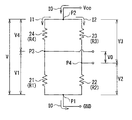
図3は、図1および図2に示した電流センサ1Aを含む電流計の回路構成を表す概略図である。図3では、破線で囲んだ部分が電流センサ1Aに対応する。図3に示したように、磁気抵抗効果素子21と磁気抵抗効果素子22とが、X方向へ延在するバスライン10を(実際にはZ方向に)挟んで互いに対向するように設けられている。ここでは磁気抵抗効果素子21,22を、複数の素子パターンが直列接続されてなる抵抗体として表している。磁気抵抗効果素子21の端部21Eと磁気抵抗効果素子22の端部22Sとは、第1の接続点P1において互いに連結され、電極膜43を介して最終的に接地されている。磁気抵抗効果素子21,22の、第1の接続点とは反対側には、第2の接続点P2において互いに連結された定電流源51,52が設けられている。具体的には、磁気抵抗効果素子21における第1の接続点P1とは反対側の端部21Sが、第3の接続点P3としての電極膜44を介して定電流源51と接続されており、一方の磁気抵抗効果素子22における第1の接続点P1とは反対側の端部22Eが、第4の接続点P4としての電極膜45を介して定電流源52と接続されている。これら定電流源51および定電流源52は、互いに等しい値の定電流I0を磁気抵抗効果素子21,22の各々へ供給するものである。
FIG. 3 is a schematic diagram showing a circuit configuration of an ammeter including the
定電流源51,52によって磁気抵抗効果素子21,22に定電流I0が流れると、補償電流線31,32には、電極膜44と電極膜45との電位差(磁気抵抗効果素子21における電圧降下と、磁気抵抗効果素子22における電圧降下との差分)に基づく補償電流Idが供給されるようになっている。電極膜44および電極膜45は、外部に設けられた差動増幅器AMPの入力側とそれぞれ接続されている。差動増幅器AMPの出力側は、電極膜47を介して補償電流線32の端部32Sと接続されている。補償電流線32の端部32Eと接続された端部31Sを有する補償電流線31は、その反対側の端部31Eが電極膜46および第5の接続点P5を介して外部の抵抗体RLと接続され、最終的に接地されている。抵抗体RLの、差動増幅器AMPの側には、第5の接続点P5において接続された補償電流検出手段Sが設けられている。ここでは、補償電流線31に補償電流Idが流れることにより、検出対象電流Imに基づいて磁気抵抗効果素子21に印加される電流磁界Hmとは逆方向の補償電流磁界Hdが磁気抵抗効果素子21に付与されるように構成されている。同様に、補償電流線32に補償電流Idが流れることにより、検出対象電流Imに基づいて磁気抵抗効果素子22に印加される電流磁界Hmとは逆方向の補償電流磁界Hdが磁気抵抗効果素子22に付与されるように構成されている。これについて、図4を参照して詳細に説明する。
When the constant current I0 flows through the
図4は、図2に示した断面構成の要部を拡大したものであり、電流の流れる方向と、その電流によって生ずる磁界の方向との関係について模式的に表している。バスライン10に対して、例えば+X方向へ(紙面奥から手前へ)向かうように検出対象電流Imが供給されると、右ねじの法則から紙面上では反時計回りの電流磁界Hmが生ずる。このため、磁気抵抗効果素子21の各素子パターン21A〜21Cに対しては+Y方向への電流磁界Hmが印加されることとなり、一方の磁気抵抗効果素子22の各素子パターン22A〜22Cに対しては−Y方向への電流磁界Hmが印加されることとなる。このとき、補償電流Idは、各素子パターン21A〜21Cに対応する巻線体部分31A〜31Cの中をそれぞれ−X方向へ(紙面手前から奥へ)向かうように流れると共に、各素子パターン22A〜22Cに対応する巻線体部分32A〜32Cの中をそれぞれ+X方向へ向かうように流れるように構成されている。したがって、右ねじの法則により、巻線体部分31A〜31Cの周囲には紙面上、時計回りの補償電流磁界Hdが生じ、一方の巻線体部分32A〜32Cの周囲には紙面上、反時計回りの補償電流磁界Hdが生じるので、結果として、各素子パターン21A〜21Cに対しては−Y方向への補償電流磁界Hdが付与され、各素子パターン22A〜22Cに対しては+Y方向への補償電流磁界Hdが印加されることとなる。すなわち、電流磁界Hmとは反対向きの補償電流磁界Hdが素子パターン21A〜21C,22A〜22Cの各々に付与される。
FIG. 4 is an enlarged view of the main part of the cross-sectional configuration shown in FIG. 2, and schematically shows the relationship between the direction of current flow and the direction of the magnetic field generated by the current. When the detection target current Im is supplied to the
次に、図5を参照して、素子パターン21A〜21C,22A〜22Cの構成について、より詳しく説明する。図5は、素子パターン21A〜21C,22A〜22Cの構成を分解して示す分解斜視図である。
Next, the configuration of the
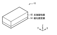
素子パターン21A〜21C,22A〜22Cは、いずれも図5に示したように、磁性層を含む複数の機能膜が積層されたスピンバルブ構造をなしており、+X方向に固着された磁化方向J11を有する固着層11と、電流磁界Hmをはじめとする外部磁界Hに応じて磁化方向J13が変化する自由層13と、固着層11と自由層13との間に挟まれ、特定の磁化方向を示さない中間層12とをそれぞれ含むものである。自由層13は、ニッケル鉄合金(NiFe)などの軟磁性材料により構成されている。中間層12は、銅(Cu)により構成され、上面が固着層11と接すると共に下面が自由層13と接している。中間層12は、銅のほか、金(Au)などの導電率の高い非磁性金属により構成することができる。なお、固着層11の上面(中間層12と反対側の面)および自由層13の下面(中間層12と反対側の面)は、それぞれ図示しない保護膜によって保護されている。また、固着層11と自由層13との間には磁化方向J11における交換バイアス磁界Hin(以下、単に「交換バイアス磁界Hin」と記す。)が生じており、中間層12を介して互いに作用し合っている。交換バイアス磁界Hinの強度は、固着層11と自由層13との相互間隔(すなわち中間層12の厚み)に応じて自由層13のスピン方向が回転することにより変化する。さらに、図5では、下から自由層13、中間層12、固着層11の順に積層された場合の構成例を示しているが、これに限定されず、反対の順序で構成するようにしてもよい。
As shown in FIG. 5, each of the
図6に、固着層11の詳細な構成を示す。固着層11は、中間層12の側から磁化固定膜14と反強磁性膜15とが順に積層された構成となっている。磁化固定膜14は、コバルト(Co)やコバルト鉄合金(CoFe)などの強磁性材料によって構成されている。この磁化固定膜14の示す磁化方向が固着層11全体としての磁化方向J11となる。反強磁性膜15は、白金マンガン合金(PtMn)やイリジウムマンガン合金(IrMn)などの反強磁性材料により構成されている。反強磁性膜15は、+X方向のスピン磁気モーメントと反対方向(−X方向)のスピン磁気モーメントとが完全に打ち消し合った状態にあり、磁化固定膜14の磁化方向J11を固定するように機能するものである。
FIG. 6 shows a detailed configuration of the
以上のように構成された素子パターン21A〜21C,22A〜22Cでは、電流磁界Hmが印加されることにより自由層13の磁化方向J13が回転し、それによって磁化方向J13と磁化方向J11との相対角度が変化する。その相対角度は、電流磁界Hmの大きさや向きによって決まるものである。
In the
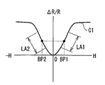
なお、図5は、電流磁界Hmが零(Hm=0)であり、かつ、その他の磁界(バイアス磁界など)を印加しない無負荷状態(すなわち、外部磁界Hが零の状態)を示している。自由層13の磁化容易軸方向AE13が固着層11の磁化方向J11と平行となるように形成されていることから、この状態では、磁化容易軸方向AE13と、磁化方向J13と、磁化方向J11とが全て+X方向に沿って互いに平行となっている。このため、自由層13における各磁区のスピン方向がほぼ同一方向に揃うこととなるので、素子パターン21A〜21C,22A〜22Cに対し、磁化方向J11と直交する方向(+Y方向または−Y方向)へ外部磁界Hが印加された場合には、図7に示したような特性が得られる。図7は、Y方向への外部磁界Hを正として外部磁界Hと抵抗変化率ΔR/Rとの関係を示したものであるが、両者の関係は、外部磁界H=0において極小(ΔR/R=0)となり、ヒステリシスをほとんど示すことのない1本の曲線C1で表される。この場合、ヒステリシスに起因する1/fノイズが極めて小さくなるので、高感度かつ安定したセンシングが可能となる。
FIG. 5 shows a no-load state where the current magnetic field Hm is zero (Hm = 0) and no other magnetic field (such as a bias magnetic field) is applied (that is, the external magnetic field H is zero). . Since the easy axis direction AE13 of the
ただし、図7から明らかなように、外部磁界Hが零(H=0)の近傍においては直線的な変化が得られないので、実際に電流磁界Hmを測定する場合には図示しない永久磁石などによるバイアス磁界を磁化方向J11と直交する方向へ印加することで、図8に示したように、磁化方向J13を回転させ、+Y方向の成分または−Y方向の成分を含むように僅かに傾ける(図6では−Y方向へ傾けた場合を例示する)。こうすることにより、図7に示したバイアスポイントBP1,BP2を中心とする線形領域LA1,LA2において電流磁界Hmの変化を精度良く検出することができる。電流センサ1Aでは、固着層11における磁化方向J11がいずれも+X方向に固着されているので、素子パターン21A〜21C,22A〜22Cの全てに対して同じ方向のバイアス磁界を印加するようにする。こうすることにより、電流磁界Hmを検出したときに、磁気抵抗効果素子21の抵抗値R1と磁気抵抗効果素子22の抵抗値R2とが互いに逆の変化を生じることとなる。例えば、素子パターン21A〜21C,22A〜22Cに対して、予め+Y方向へバイアスポイントBP1(図7参照)に相当する強度のバイアス磁界を印加しておく。図4に示したように+X方向へ検出対象電流Imを流したときには、素子パターン21A〜21Cは、+Y方向の電流磁界Hmが印加されるので、図7から明らかなように抵抗変化率が増加する(抵抗値R1が増加する)。これに対し、素子パターン22A〜22Cは、−Y方向の電流磁界Hmが印加されるので、図7から明らかなように抵抗変化率が減少する(抵抗値R2が減少する)のである。
However, as apparent from FIG. 7, since a linear change cannot be obtained in the vicinity of the external magnetic field H being zero (H = 0), a permanent magnet or the like (not shown) is used when actually measuring the current magnetic field Hm. Is applied in a direction perpendicular to the magnetization direction J11, the magnetization direction J13 is rotated and slightly tilted so as to include a component in the + Y direction or a component in the -Y direction (see FIG. 8). FIG. 6 shows an example in which it is tilted in the −Y direction. By so doing, it is possible to accurately detect a change in the current magnetic field Hm in the linear regions LA1 and LA2 centered on the bias points BP1 and BP2 shown in FIG. In the
このような構成の電流センサ1Aでは、第1の接続点P1と第2の接続点P2との間に電圧が印加されたときに、第3および第4の接続点P3,P4における電位の差分V0(磁気抵抗効果素子21,22のそれぞれに生ずる電圧降下の差分)に基づく補償電流Idが差動増幅器AMPを介して補償電流線31,32を流れ、その補償電流Idが補償電流検出手段Sによって検出されるようになっている。差動増幅器AMPは、差分V0が零となるように補償電流Idを調整するものである。
In the
以下、再び図3を参照して、検出対象電流Imによって形成される電流磁界Hmを測定する方法について説明する。 Hereinafter, a method of measuring the current magnetic field Hm formed by the detection target current Im will be described with reference to FIG. 3 again.
図3において、第1の接続点P1と第2の接続点P2との間に所定の電圧を印加した際の定電流源51,52からの定電流をI0とし、磁気抵抗効果素子21,22全体の抵抗値をそれぞれR1,R2とする。電流磁界Hmが印加されていない場合、第3の接続点P3(電極膜44)における電位V1は、
V1=I0・R1
であり、第4の接続点P4(電極膜45)における電位V2は、
V2=I0・R2
となる。よって、第3の接続点P3と第4の接続点P4との間の電位差は、
V0=V1−V2
=I0・R1−I0・R2
=I0・(R1−R2) …(1)
In FIG. 3, the constant current from the constant
V1 = I0 ・ R1
The potential V2 at the fourth connection point P4 (electrode film 45) is
V2 = I0 · R2
It becomes. Therefore, the potential difference between the third connection point P3 and the fourth connection point P4 is
V0 = V1-V2
= I0 · R1-I0 · R2
= I0 · (R1-R2) (1)
この回路では、電流磁界Hmが印加されたときに、電位差V0を測定することにより磁気抵抗効果素子21,22における抵抗変化量が得られる。例えば電流磁界Hmが印加されたときに、抵抗値R1,R2がそれぞれ変化量ΔR1,ΔR2だけ増加したとすると、式(1)は、
V0=V1−V2
=I0・(R1−R2)
=I0・{(R1+ΔR1)−(R2+ΔR2)} …(2)
となる。
In this circuit, when the current magnetic field Hm is applied, the resistance change amount in the
V0 = V1-V2
= I0 · (R1-R2)
= I0 · {(R1 + ΔR1) − (R2 + ΔR2)} (2)
It becomes.
すでに述べたように、磁気抵抗効果素子21(素子パターン21A〜21C)と磁気抵抗効果素子22(素子パターン22A〜22C)とは電流磁界Hmによって各々の抵抗値R1,R2が互いに逆方向の変化を示すように配置されていることから、変化量ΔR1と変化量ΔR2とは互いの正負が逆の符号となる。したがって、式(2)において、電流磁界Hmが印加される前の抵抗値R1および抵抗値R2は互いに打ち消し合う一方で、変化量ΔR1および変化量ΔR2はそのまま維持される。
As already described, the resistance values R1 and R2 of the magnetoresistive effect element 21 (
仮に、磁気抵抗効果素子21と磁気抵抗効果素子22とが全く同一の特性を有するとした場合、すなわち、
R1=R2=R
かつ
ΔR1=−ΔR2=ΔR
であると仮定した場合、式(3)は、
V0=I0・(R1+ΔR1−R2−ΔR2)
=I0・(R+ΔR−R+ΔR)
=I0・(2ΔR) …(4)
となる。したがって、予め外部磁界と抵抗変化量との関係を把握した磁気抵抗効果素子21,22を用いるようにすれば、電流磁界Hmの大きさを求めることができ、その大きさの電流磁界Hmを発生する検出対象電流Imの大きさを推定することができる。この場合、2つの磁気抵抗効果素子21,22を用いてセンシングを行っているので、磁気抵抗効果素子21または磁気抵抗効果素子22を単独で用いてセンシングを行う場合と比べて2倍の抵抗変化量を取り出すことができ、測定値の高精度化に有利となる。
If the
R1 = R2 = R
And ΔR1 = −ΔR2 = ΔR
Assuming that
V0 = I0 · (R1 + ΔR1-R2-ΔR2)
= I0 · (R + ΔR-R + ΔR)
= I0 · (2ΔR) (4)
It becomes. Therefore, if the
さらに、電流センサ1Aでは、第3の接続点P3において検出される電位V1と第4の接続点P4において検出される電位V2とが差動増幅器AMPに供給されて、その差分(電位差V0)が零となるような補償電流Idが出力される。差動増幅器AMPからの補償電流Idは、電流磁界Hmとは逆方向の補償電流磁界Hdを各素子パターン21A〜21C,22A〜22Cへ付与し、回路中の接続抵抗のばらつきや磁気抵抗効果素子21,22の相互間における特性のばらつき、温度分布の偏り、あるいは外部からの妨害磁界などに起因する誤差分をキャンセルするように作用するので、結果として電流磁界Hmのみに比例した大きさに近づくこととなる。したがって、補償電流検出手段Sにおいて、出力電圧Voutを測定し、既知の抵抗体RLとの関係から補償電流Idを算出することにより、より正確な電流磁界Hmを求めることができ、ひいては検出対象電流Imの大きさを高精度に推定することができる。
Further, in the
以上のように、本実施の形態の電流センサ1Aによれば、第1の階層L1においてX方向に延在すると共に検出対象電流Imが供給されるバスライン10と、第2の階層L2のバスライン10と対応する領域においてX方向に延在すると共に電流磁界Hmに応じて抵抗値R1が変化する素子パターン21A〜21Cを含む磁気抵抗効果素子21と、第3の階層L3のバスライン10と対応する領域においてX方向に延在すると共に電流磁界Hmに応じて抵抗値R2が変化する素子パターン22A〜22Cを含む磁気抵抗効果素子22とを備えるようにしたので、磁気抵抗効果素子21,22をバスライン10に対して比較的近くに配置することができ、コンパクト化を図りつつ電流磁界Hmを感度良く検出することができる。さらに、抵抗値R1と抵抗値R2とが電流磁界Hmによって互いに逆方向の変化(増減)を示すので、それらの抵抗値の差分を検出することによって、高精度に検出対象電流を測定することができる。特に、磁気抵抗効果素子21,22の各々に対して互いに等しい値の定電流I0を流したときに生ずる電圧降下の差分V0を検出するようにしたので、測定結果の信頼性が向上する。
As described above, according to the
さらに、補償電流線31,32を第4および第5の階層L4,L5にそれぞれ設け、電圧降下の差分V0に応じた補償電流Idをそれぞれに流すようにしたので、各素子パターン21A〜21C,22A〜22Cに対して電流磁界Hmとは逆方向の補償電流磁界Hdを付与することができ、磁気抵抗効果素子21と磁気抵抗効果素子22との特性上のばらつきや、回路中の接続抵抗のばらつき、あるいは温度分布に起因した誤差をキャンセルすることができ、よりいっそう高精度に検出対象電流Imを測定することができる。
Furthermore, since the compensation
さらに、素子パターン21A〜21C,22A〜22Cを、それぞれ、X方向に延在すると共にY方向に互いに隣在し合うように配設して直列接続するようにしたので、X方向における寸法を長くすることなく感磁部として機能する素子パターン21A〜21C,22A〜22Cのそれぞれの総延長を稼ぐことができ、磁気抵抗効果素子21,22のそれぞれにおける全体のインピーダンスの絶対値を稼ぐことができる。したがって、より微弱な検出対象電流Imであっても高精度に測定することができる。この際、補償電流線31が素子パターン21A〜21Cの各々と対応する巻線体部分31A〜31Cを有し、かつ、補償電流線32が素子パターン22A〜22Cの各々と対応する巻線体部分32A〜32Cを有するように構成したので、素子パターン21A〜21C,22A〜22Cの各々に対して、より均一な大きさの補償電流磁界Hdを付与することができ、被検出対象電流Imの測定値の精度をさらに高めることができる。
Furthermore, since the
[第2の実施の形態]
続いて、図9および図10を参照して、本発明の第2の実施の形態としての電流センサ1Bについて説明する。
[Second Embodiment]
Subsequently, a
電流センサ1Bは、上記第1の実施の形態の電流センサ1Aの構成に、さらに第3および第4の磁気抵抗効果素子23,24(以下、単に「磁気抵抗効果素子23,24」という。)を加えるようにしたものである。以下、具体的に説明するが、上記第1の実施の形態と重複する部分については適宜説明を省略する。
In the
図9は、電流センサ1Bの斜視構成を表す概略図である。図9に示したように、電流センサ1Bでは、磁気抵抗効果素子23が第2の階層L2において磁気抵抗効果素子21と隣り合うようにX方向に並んで配置されていると共に、磁気抵抗効果素子24が第3の階層L3において磁気抵抗効果素子22と隣り合うようにX方向に並んで配置されている。磁気抵抗効果素子23は、積層方向においてバスライン10と対応する領域のうち、磁気抵抗効果素子21が形成された領域以外の領域においてX方向に延在する複数の素子パターン23A〜23Cを含んで構成されている。同様に、磁気抵抗効果素子24は、積層方向においてバスライン10と対応する領域のうち、磁気抵抗効果素子22が形成された領域以外の領域においてX方向に延在する複数の素子パターン24A〜24Cを含んで構成されている。ここで、素子パターン23A〜23Cは、磁気抵抗効果素子23の全体としての抵抗値R3が電流磁界Hmに応じて磁気抵抗効果素子21の全体としての抵抗値R1と同方向へ変化するようになっている。一方、素子パターン24A〜24Cは、磁気抵抗効果素子24の全体としての抵抗値R4が電流磁界Hmに応じて磁気抵抗効果素子22の全体としての抵抗値R2と同方向へ変化するようになっている。
FIG. 9 is a schematic diagram illustrating a perspective configuration of the
素子パターン23A〜23Cは、X方向に延在すると共にY方向に互いに隣在し合うように配設されて直列接続されている。すなわち、磁気抵抗効果素子23は、端部23Sと端部23Eとの間でつづら折り状に連なっており、その平行部分に素子パターン23A〜23Cが配置されている。磁気抵抗効果素子24においても同様に、端部24Sと端部24Eとの間でつづら折り状に連なった形状をなしており、その平行部分に素子パターン24A〜24Cが配置されている。ここで、素子パターン23A〜23Cは、それぞれ、素子パターン21A〜21Cの各々とX方向に延びる同一直線上に配置されており、素子パターン24A〜24Cは、それぞれ、素子パターン22A〜22Cの各々と、X方向に延びる同一直線上に配置されている。ここで、端部23Eと端部24Sとがコンタクト層T13などを介して互いに連結されている。端部24Sは、コンタクト層T14などを介して絶縁膜Z5上の電極膜48と接続されている。さらに、端部23Sはコンタクト層T15〜T17などを介して絶縁膜Z5上の電極膜49と接続されており、端部24Eはコンタクト層T18などを介して絶縁膜Z5上の電極膜50と接続されている。
The
また、電流センサ1Bでは、補償電流線31が、素子パターン21A〜21C21および素子パターン23A〜23Cの双方と対応してX方向へ延在する巻線体部分31A〜31Cを含んで第4の階層L4内を巻回するように設けられている。さらに、補償電流線32が、素子パターン22A〜22C21および素子パターン24A〜24Cの双方と対応してX方向へ延在する巻線体部分32A〜32Cを含んで第5の階層L5内を巻回するように設けられている。ここで、端部32Eと端部31Sとがコンタクト層(図示せず)を介して互いに連結されているので、補償電流線31,32は回路構成上、1本の電流線となっている。なお、端部32Sはコンタクト層T9を介して電極膜47と接続されており、端部31Eはコンタクト層T10〜T12を順に介して電極膜46と接続されている。
Further, in the
図10は、図9に示した電流センサ1Bを含む電流計の回路構成を表す概略図である。図10では、破線で囲んだ部分が電流センサ1Bに対応する。図10に示したように、磁気抵抗効果素子21および磁気抵抗効果素子22が、第1の接続点P1において互いに連結され、電極膜43を介して最終的に接地されている。また、磁気抵抗効果素子23と磁気抵抗効果素子24とが、第2の接続点P2において互いに接続されている。さらに、磁気抵抗効果素子21における第1の接続点P1とは反対側の端部21Sと磁気抵抗効果素子24における第2の接続点P2とは反対側の端部24Eとが、第3の接続点P3としての電極膜44において接続され、かつ、磁気抵抗効果素子22における第1の接続点P1とは反対側の端部22Eと磁気抵抗効果素子23における第2の接続点P2とは反対側の端部23Sとが、第4の接続点P4としての電極膜45において接続されている。このように、第1の接続点P1と第2の接続点P2との間に電圧が印加されたときの第3の接続点P3と第4の接続点P4との間の電位差V0に基づいて検出対象電流Imが検出されるようにブリッジ回路が構成されている。
10 is a schematic diagram illustrating a circuit configuration of an ammeter including the
磁気抵抗効果素子21〜24に読出電流I0が流れると、補償電流線31,32には、第3の接続点P3と第4の接続点P4との電位差に基づく補償電流Idが供給されるようになっている。ここでは、補償電流線31に補償電流Idが流れることにより、検出対象電流Imに基づいて磁気抵抗効果素子21,23に印加される電流磁界Hmとは逆方向の補償電流磁界Hdが磁気抵抗効果素子21,23に付与されるように構成されている。同様に、補償電流線32に補償電流Idが流れることにより、検出対象電流Imに基づいて磁気抵抗効果素子22,24に印加される電流磁界Hmとは逆方向の補償電流磁界Hdが磁気抵抗効果素子22,24に付与されるように構成されている(図4参照)。
When the read current I0 flows through the
このような構成の電流センサ1Bでは、補償電流Idを補償電流検出手段Sによって検出することにより、検出対象電流Imを推定するようにしている。以下、図10に加え、図11を参照して、検出対象電流Imによって形成される電流磁界Hmを測定する方法について説明する。図11は、図10の要部を簡略化して示した回路図である。
In the
図11では、電流磁界Hmが印加されていない状態で読出電流I0を流したときの磁気抵抗効果素子21〜24の抵抗値をそれぞれ符号R1〜R4で示す。読出電流I0は第2の接続点P2で分流される。こののち、磁気抵抗効果素子24,21を通過する読出電流I1と磁気抵抗効果素子23,21を通過する読出電流I2とが第1の接続点P1で合流する。この場合、第2の接続点P2と第1の接続点P1との間の電位差Vは、
V=I1・R4+I1・R1=I2・R3+I2・R2
=I1(R4+R1)=I2(R3+R2) ……(5)
と表すことができる。
また、第3の接続点P3における電位V1および第4の接続点P4における電位V2は、それぞれ、
V1=V−V4
=V−I1・R4
V2=V−V3
=V−I2・R3
と表せる。よって、第3の接続点P3と第4の接続点P4との間の電位差V0は、
V0=V1−V2
=(V−I1・R4)−(V−I2・R3)
=I2・R3−I1・R4 ……(6)
ここで、(5)式から
V0=R3/(R3+R2)・V−R4/(R4+R1)・V
={R3/(R3+R2)−R4/(R4+R1)}・V ……(7)
となる。このブリッジ回路では、電流磁界Hmが印加されたときに、上記の式(7)で示された第3および第4の接続点P3,P4間の電圧V0を測定することにより、抵抗変化量が得られる。電流磁界Hmが印加されたときに、抵抗値R1〜R4がそれぞれ変化量ΔR1〜ΔR1だけ増加したとすると、すなわち、抵抗値R1〜R4がそれぞれ、
R1→R1+ΔR1
R2→R2+ΔR2
R3→R3+ΔR3
R4→R4+ΔR4
のように変化したとすると、電流磁界Hmを印加後は、式(7)より、
V0={(R3+ΔR3)/(R3+ΔR3+R2+ΔR2)−(R4+ΔR4)/(R4+ΔR4+R1+ΔR1)}・V ……(8)
となる。すでに述べたように、電流センサ1Bでは、磁気抵抗効果素子21,23の抵抗値R1,R3と磁気抵抗効果素子22,24の抵抗値R2,R4とが逆方向に変化する(磁気抵抗効果素子21,23と磁気抵抗効果素子22,24とでは逆方向に電流磁界Hmが印加されることから、磁気抵抗効果素子21〜24の全てに対して、同一方向のバイアス磁界を予め印加するようにする。)ので、変化量ΔR3と変化量ΔR2とが打ち消し合うと共に変化量ΔR4と変化量ΔR1とが打ち消し合うこととなる。このため、電流磁界Hmの印加前後を比較した場合、式(8)の各項における分母の増加はほとんど無い。一方、各項の分子については、変化量ΔR3と変化量ΔR4とは必ず反対の符号を有するので、打ち消し合うことなく増減が現れることとなる。これは、図7から明らかなように、バイアス点BP1に対応するバイアス磁界が予め印加された状態において+Y方向の電流磁界Hmが印加されることにより、磁気抵抗効果素子22,24では、抵抗値は変化量ΔR2,ΔR4(ΔR2,ΔR4<0)の分だけそれぞれ変化する(実質的に低下する)一方で、磁気抵抗効果素子21,23では、抵抗値は変化量ΔR1,ΔR3(ΔR1,ΔR3>0)の分だけそれぞれ変化する(実質的に増加する)からである。
In FIG. 11, the resistance values of the
V = I1 · R4 + I1 · R1 = I2 · R3 + I2 · R2
= I1 (R4 + R1) = I2 (R3 + R2) (5)
It can be expressed as.
The potential V1 at the third connection point P3 and the potential V2 at the fourth connection point P4 are respectively
V1 = V-V4
= V-I1 ・ R4
V2 = V-V3
= V-I2 ・ R3
It can be expressed. Therefore, the potential difference V0 between the third connection point P3 and the fourth connection point P4 is
V0 = V1-V2
= (V-I1 * R4)-(V-I2 * R3)
= I2 / R3-I1 / R4 (6)
Here, V0 = R3 / (R3 + R2) .V-R4 / (R4 + R1) .V from the equation (5).
= {R3 / (R3 + R2) -R4 / (R4 + R1)}. V (7)
It becomes. In this bridge circuit, when the current magnetic field Hm is applied, the resistance change amount is obtained by measuring the voltage V0 between the third and fourth connection points P3 and P4 expressed by the above equation (7). can get. If the resistance values R1 to R4 are increased by the change amounts ΔR1 to ΔR1 when the current magnetic field Hm is applied, that is, the resistance values R1 to R4 are respectively
R1 → R1 + ΔR1
R2 → R2 + ΔR2
R3 → R3 + ΔR3
R4 → R4 + ΔR4
If the current magnetic field Hm is applied, the equation (7)
V0 = {(R3 + ΔR3) / (R3 + ΔR3 + R2 + ΔR2) − (R4 + ΔR4) / (R4 + ΔR4 + R1 + ΔR1)} · V (8)
It becomes. As already described, in the
仮に、磁気抵抗効果素子21〜24が完全に同一の特性を有するとした場合、すなわち、
R=R1=R2=R3=R4
かつ
ΔR=ΔR1=−ΔR2=ΔR3=−ΔR4
であるとした場合、式(8)は、
V0={(R+ΔR)/(2R)−(R−ΔR)/(2R)}・V
=(ΔR/R)・V
となる。
If the
R = R1 = R2 = R3 = R4
And ΔR = ΔR1 = −ΔR2 = ΔR3 = −ΔR4
(8) is given by
V0 = {(R + ΔR) / (2R) − (R−ΔR) / (2R)} · V
= (ΔR / R) · V
It becomes.
このように、予め抵抗変化率ΔR/R等の特性値を把握した磁気抵抗効果素子21〜24を用いることにより、電流磁界Hmの大きさを求めることができ、その電流磁界Hmを発生する検出対象電流Imの大きさを推定することができる。特に、ブリッジ回路を構成してセンシングを行うようにすることにより、同等の出力を有する単一の素子パターンによりセンシングする場合と比べて、各磁気抵抗効果素子の素子パターンにおける抵抗変化量を大きく取り出すことができ、測定値の精度を向上させることが可能である。また、本実施の形態では、磁気抵抗効果素子21〜24の全ての固着層11の磁化方向J11を同一方向をなすようにしたので、電流磁界Hmの方向に対して、磁化方向J11が全て同一角度をなすこととなる。このため、磁気抵抗効果素子21〜24における検出感度のばらつきを抑えることが比較的容易である。
As described above, by using the
さらに、電流センサ1Bでは、第3の接続点P3において検出される電位V1と第4の接続点P4において検出される電位V2とが差動増幅器AMPに供給されて、その差分(電位差V0)が零となるような補償電流Idが出力される。差動増幅器AMPからの補償電流Idは、電流磁界Hmとは逆方向の補償電流磁界Hdを各素子パターン21A〜21C,22A〜22C,23A〜23C,24A〜24Cへ付与し、回路中の接続抵抗のばらつきや磁気抵抗効果素子21〜24の相互間における特性のばらつき、温度分布の偏り、あるいは外部からの妨害磁界などに起因する誤差分をキャンセルするように作用するので、結果として電流磁界Hmのみに比例した大きさに近づくこととなる。したがって、補償電流検出手段Sにおいて、出力電圧Voutを測定し、既知の抵抗体RLとの関係から補償電流Idを算出することにより、より正確な電流磁界Hmを求めることができ、ひいては検出対象電流Imの大きさを高精度に推定することができる。
Further, in the
以上のように、本実施の形態の電流センサ1Bによれば、上記第1の実施の形態における電流センサ1Aに加えて、磁気抵抗効果素子23,24を加えるようにしたので、ブリッジ回路を構成してセンシングを行うことが可能となり、被検出対象電流Imの測定値の精度をさらに高めることができる。この場合、磁気抵抗効果素子21と同じ第2の階層L2に磁気抵抗効果素子23を設けると共に磁気抵抗効果素子22と同じ第3の階層L3に磁気抵抗効果素子24を設けるようにしたことに加え、磁気抵抗効果素子21および磁気抵抗効果素子23が補償電流線31を共有すると共に磁気抵抗効果素子22および磁気抵抗効果素子24が補償電流線32を共有するようにしたので、全体としてコンパクトな構成を維持することができる。
As described above, according to the
以上、実施の形態を挙げて本発明を説明したが、本発明は実施の形態に限定されず、種々の変形が可能である。例えば本実施の形態では、磁気抵抗効果素子における複数の素子パターンを直列接続するように構成したが、これに限定されず、例えば図12に示した変形例としての電流センサ1Cのように並列接続するようにしてもよい。その場合には、コンパクトな構成を維持しつつ、抵抗変化率ΔR/Rを下げることなく全体のインピーダンスを低減することができ、外部からのノイズ(不要な磁界)による影響を低下させ、SN比を向上させることができる。この場合にも、第1の補償電流線31を、第1の磁気抵抗効果素子21における各素子パターン21A〜21Cと対応して第1の方向に延在する巻線体部分31A〜31Cを含んで第4の階層内を巻回するように構成し、かつ、第2の補償電流線32を、第2の磁気抵抗効果素子22における各素子パターン22A〜22Cと対応して第1の方向に延在する巻線体部分32A〜32Cを含んで第5の階層内を巻回するように構成すると、各素子パターン21A〜21C,22A〜22Cに対して、より適切な大きさの補償電流磁界Hdを付与することができ、検出対象電流Imの測定値の精度がさらに高まるという利点が得られる。
Although the present invention has been described with reference to the embodiment, the present invention is not limited to the embodiment, and various modifications can be made. For example, in the present embodiment, the plurality of element patterns in the magnetoresistive effect element are configured to be connected in series. However, the present invention is not limited to this. For example, the current sensor 1C as a modification shown in FIG. You may make it do. In that case, the overall impedance can be reduced without decreasing the resistance change rate ΔR / R while maintaining a compact configuration, and the influence of external noise (unnecessary magnetic field) is reduced, and the SN ratio is reduced. Can be improved. Also in this case, the first compensation
また、第2の実施の形態では、第1および第3の磁気抵抗効果素子が第1の補償電流線を共有し、第2および第3の磁気抵抗効果素子が第2の補償電流線を共有するようにしたが、これに限定されず、第3の磁気抵抗効果素子と対応する第3の補償電流線を設けたり、第4の磁気抵抗効果素子と対応する第4の補償電流線を設けるようにしてもよい。 In the second embodiment, the first and third magnetoresistive elements share the first compensation current line, and the second and third magnetoresistive elements share the second compensation current line. However, the present invention is not limited to this, and a third compensation current line corresponding to the third magnetoresistance effect element is provided, or a fourth compensation current line corresponding to the fourth magnetoresistance effect element is provided. You may do it.
さらに、本実施の形態では、固着層の磁化方向と自由層の磁化容易軸方向とが互いに一致したスピンバルブ構造を有する素子パターンを採用するようにしたが、これに限定されるものではない。例えば、固着層の磁化方向と自由層の磁化容易軸方向とが互いに直交するスピンバルブ構造を有する素子パターンを用いるようにしてもよい。 Furthermore, in the present embodiment, an element pattern having a spin valve structure in which the magnetization direction of the pinned layer and the magnetization easy axis direction of the free layer coincide with each other is adopted. However, the present invention is not limited to this. For example, an element pattern having a spin valve structure in which the magnetization direction of the pinned layer and the magnetization easy axis direction of the free layer are orthogonal to each other may be used.
本発明の電流センサは、上記実施の形態において説明したように、電流値そのものを図ることを目的とする場合に用いられるほか、プリント配線の欠陥などの検査を行う渦電流探傷技術に応用可能である。例えば、素子パターンを直線上に多数個配置した電流センサとし、渦電流の変化を磁束の変化として捉えるような応用例が考えられる。 As described in the above embodiment, the current sensor of the present invention is used for the purpose of measuring the current value itself, and can be applied to eddy current flaw detection technology for inspecting printed wiring defects and the like. is there. For example, an application example may be considered in which a current sensor in which a large number of element patterns are arranged on a straight line is used, and a change in eddy current is captured as a change in magnetic flux.
1…電流センサ、2…基体、10…バスライン、21〜24…第1〜第4の磁気抵抗効果素子、31,32…第1,第2の補償電流線、41〜50…電極膜、L1〜L5…第1〜第5の階層、P1〜P5…第1〜第5の接続点。
DESCRIPTION OF
Claims (3)
前記第1の階層と異なる第2の階層の前記導体と対応する領域において前記第1の方向に延在すると共に前記第1の方向と直交する第2の方向に互いに隣在し合うように配設されて直列接続または並列接続された複数の素子パターンを有し、かつ、前記導体に流れる検出対象電流により生ずる電流磁界に応じて抵抗値が変化する第1の磁気抵抗効果素子と、
前記第1の階層を基準として前記第2の階層と反対側に位置する第3の階層の前記導体と対応する領域において前記第1の方向に延在すると共に前記第2の方向に互いに隣在し合うように配設されて直列接続または並列接続された複数の素子パターンを有し、かつ、前記電流磁界に応じて前記第1の磁気抵抗効果素子とは逆方向に抵抗値が変化する第2の磁気抵抗効果素子と、
前記第2の階層と隣接する第4の階層において前記第1の磁気抵抗効果素子の各素子パターンと対応して前記第1の方向に延在する複数の第1の巻線体部分を含んで巻回するように構成され、前記第1および第2の磁気抵抗効果素子の各々に対して互いに等しい値の定電流を流したときに生ずる電圧降下の差分に応じた補償電流が流れることにより、前記検出対象電流に基づいて前記第1の磁気抵抗効果素子に印加される電流磁界とは逆方向の補償電流磁界を前記第1の磁気抵抗効果素子の各素子パターンに対して対応する前記第1の巻線体部分からそれぞれ付与するように構成された第1の補償電流線と、
前記第3の階層と隣接する第5の階層において前記第2の磁気抵抗効果素子の各素子パターンと対応して前記第1の方向に延在する複数の第2の巻線体部分を含んで巻回するように構成され、前記電圧降下の差分に応じた補償電流が流れることにより、前記検出対象電流に基づいて前記第2の磁気抵抗効果素子に印加される電流磁界とは逆方向の補償電流磁界を前記第2の磁気抵抗効果素子の各素子パターンに対して対応する前記第2の巻線体部分からそれぞれ付与するように構成された第2の補償電流線と、
を備え、
前記電圧降下の差分に基づいて前記検出対象電流を検出する
ことを特徴とする電流センサ。 A conductor extending in the first direction in the first hierarchy and supplied with a current to be detected;
In a region corresponding to the conductor of the second layer different from the first layer, the region extends in the first direction and is adjacent to each other in a second direction orthogonal to the first direction. A first magnetoresistive element having a plurality of element patterns connected in series or in parallel and having a resistance value that changes in accordance with a current magnetic field generated by a current to be detected flowing in the conductor;
Each other in the second direction while extending in the first direction in the conductor and the corresponding region of the third hierarchy which lies opposite the front Stories second hierarchy with respect to the first hierarchy It has a plurality of element patterns arranged so as to be adjacent to each other and connected in series or in parallel, and the resistance value changes in a direction opposite to that of the first magnetoresistive element in accordance with the current magnetic field. A second magnetoresistive effect element ,
A plurality of first winding body portions extending in the first direction corresponding to each element pattern of the first magnetoresistance effect element in a fourth layer adjacent to the second layer; A compensation current corresponding to a difference in voltage drop that occurs when a constant current having a value equal to each other is supplied to each of the first and second magnetoresistive elements is configured to be wound. The compensation current magnetic field in the direction opposite to the current magnetic field applied to the first magnetoresistance effect element based on the detection target current corresponds to each element pattern of the first magnetoresistance effect element. A first compensating current line configured to be applied from each of the winding body parts of
A plurality of second winding body portions extending in the first direction corresponding to each element pattern of the second magnetoresistance effect element in a fifth layer adjacent to the third layer; Compensation in a direction opposite to the current magnetic field applied to the second magnetoresistive effect element based on the current to be detected by flowing a compensation current according to the difference of the voltage drop. A second compensation current line configured to apply a current magnetic field from the second winding body portion corresponding to each element pattern of the second magnetoresistive element;
With
A current sensor for detecting the current to be detected based on the difference in voltage drop .
前記第1の階層と異なる第2の階層の前記導体と対応する領域において前記第1の方向に延在すると共に前記第1の方向と直交する第2の方向に互いに隣在し合うように配設されて直列接続または並列接続された複数の素子パターンを有し、かつ、前記導体に流れる検出対象電流により生ずる電流磁界に応じて抵抗値が変化する第1の磁気抵抗効果素子と、
前記第1の階層を基準として前記第2の階層と反対側に位置する第3の階層の前記導体と対応する領域において前記第1の方向に延在すると共に前記第2の方向に互いに隣在し合うように配設されて直列接続または並列接続された複数の素子パターンを有し、かつ、前記電流磁界に応じて前記第1の磁気抵抗効果素子とは逆方向に抵抗値が変化し、その一端が前記第1の磁気抵抗効果素子の一端と第1の接続点において接続された第2の磁気抵抗効果素子と、
前記第2の階層における前記導体と対応する領域のうち、前記第1の磁気抵抗効果素子が形成された領域以外の領域において前記第1の方向に延在すると共に前記第2の方向に互いに隣在し合うように配設されて直列接続または並列接続された複数の素子パターンを有し、かつ、前記電流磁界に応じて抵抗値が前記第1の磁気抵抗効果素子と同方向へ変化するように構成され、その一端が前記第2の磁気抵抗効果素子の他端と第4の接続点において接続された第3の磁気抵抗効果素子と、
前記第3の階層における前記導体と対応する領域のうち、前記第2の磁気抵抗効果素子が形成された領域以外の領域において前記第1の方向に延在すると共に前記第1の方向と直交する第2の方向に互いに隣在し合うように配設されて直列接続または並列接続された複数の素子パターンを有し、かつ、前記電流磁界に応じて抵抗値が前記第1の磁気抵抗効果素子とは逆方向へ変化するように構成され、その一端が前記第3の磁気抵抗効果素子の他端と第2の接続点において接続されると共に他端が前記第1の磁気抵抗効果素子の他端と第3の接続点において接続された第4の磁気抵抗効果素子と、
前記第2の階層と隣接する第4の階層において前記第1および第3の磁気抵抗効果素子の双方の各素子パターンと対応して前記第1の方向へ延在する複数の第1の巻線体部分を含んで巻回するように構成され、前記第1の接続点と前記第2の接続点との間に電圧が印加されたときに生ずる前記第3の接続点と前記第4の接続点との間の電位差に応じた補償電流が流れることにより、前記検出対象電流に基づいて前記第1および第3の磁気抵抗効果素子に印加される電流磁界とは逆方向の補償電流磁界を前記第1および第3の磁気抵抗効果素子の各素子パターンに対して対応する前記第1の巻線体部分からそれぞれ付与するように構成された第1の補償電流線と、
前記第3の階層と隣接する第5の階層において前記第2および第4の磁気抵抗効果素子の双方の各素子パターンと対応して前記第1の方向へ延在する複数の第2の巻線体部分を含んで巻回するように構成され、前記電位差に応じた補償電流が流れることにより、前記検出対象電流に基づいて前記第2および第4の磁気抵抗効果素子に印加される電流磁界とは逆方向の補償電流磁界を前記第2および第4の磁気抵抗効果素子の各素子パターンに対して対応する前記第2の巻線体部分からそれぞれ付与するように構成された第2の補償電流線と
を備え、前記電位差に基づいて前記検出対象電流が検出されるようにブリッジ回路が構成されている
ことを特徴とする電流センサ。 A conductor extending in the first direction in the first hierarchy and supplied with a current to be detected;
In a region corresponding to the conductor of the second layer different from the first layer, the region extends in the first direction and is adjacent to each other in a second direction orthogonal to the first direction. A first magnetoresistive element having a plurality of element patterns connected in series or in parallel and having a resistance value that changes in accordance with a current magnetic field generated by a current to be detected flowing in the conductor;
Extending in the first direction and adjacent to each other in the second direction in a region corresponding to the conductor of the third layer located on the opposite side of the second layer with respect to the first layer A plurality of element patterns arranged in series and connected in series or in parallel, and the resistance value changes in the opposite direction to the first magnetoresistive element in accordance with the current magnetic field; A second magnetoresistive element having one end connected to one end of the first magnetoresistive element at a first connection point;
Of the region corresponding to the conductor in the second layer, the region extends in the first direction and is adjacent to the second direction in regions other than the region where the first magnetoresistive element is formed. It has a plurality of element patterns arranged in series and connected in series or in parallel, and the resistance value changes in the same direction as the first magnetoresistance effect element in accordance with the current magnetic field. A third magnetoresistive element having one end connected to the other end of the second magnetoresistive element at a fourth connection point ;
Of the region corresponding to the conductor in the third layer, the region extends in the first direction in the region other than the region where the second magnetoresistive element is formed and is orthogonal to the first direction. The first magnetoresistive element having a plurality of element patterns arranged adjacent to each other in the second direction and connected in series or in parallel, and having a resistance value corresponding to the current magnetic field The other end of the third magnetoresistive effect element is connected to the other end of the third magnetoresistive effect element at the second connection point, and the other end is connected to the other end of the first magnetoresistive effect element. A fourth magnetoresistive element connected to the end at the third connection point ;
A plurality of first windings extending in the first direction corresponding to the element patterns of both the first and third magnetoresistive elements in a fourth layer adjacent to the second layer The third connection point and the fourth connection, which are configured to be wound including a body part and are generated when a voltage is applied between the first connection point and the second connection point. When a compensation current corresponding to the potential difference between the points flows, a compensation current magnetic field in a direction opposite to the current magnetic field applied to the first and third magnetoresistive elements based on the detection target current is generated. A first compensation current line configured to be applied from the corresponding first winding body portion to each element pattern of the first and third magnetoresistive elements;
A plurality of second windings extending in the first direction corresponding to the element patterns of both the second and fourth magnetoresistive elements in the fifth layer adjacent to the third layer A current magnetic field applied to the second and fourth magnetoresistive elements based on the current to be detected by flowing a compensation current corresponding to the potential difference, Is a second compensation current configured to apply a compensation current magnetic field in the reverse direction from the second winding body portion corresponding to each element pattern of the second and fourth magnetoresistive elements. Lines and
And a bridge circuit is configured to detect the detection target current based on the potential difference.
A current sensor characterized by that.
ことを特徴とする請求項1または請求項2に記載の電流センサ。The current sensor according to claim 1, wherein the current sensor is a current sensor.
Priority Applications (2)
| Application Number | Priority Date | Filing Date | Title |
|---|---|---|---|
| JP2004313539A JP4105142B2 (en) | 2004-10-28 | 2004-10-28 | Current sensor |
| US11/252,570 US7495541B2 (en) | 2004-10-28 | 2005-10-19 | Current sensor |
Applications Claiming Priority (1)
| Application Number | Priority Date | Filing Date | Title |
|---|---|---|---|
| JP2004313539A JP4105142B2 (en) | 2004-10-28 | 2004-10-28 | Current sensor |
Publications (2)
| Publication Number | Publication Date |
|---|---|
| JP2006125962A JP2006125962A (en) | 2006-05-18 |
| JP4105142B2 true JP4105142B2 (en) | 2008-06-25 |
Family
ID=36261146
Family Applications (1)
| Application Number | Title | Priority Date | Filing Date |
|---|---|---|---|
| JP2004313539A Active JP4105142B2 (en) | 2004-10-28 | 2004-10-28 | Current sensor |
Country Status (2)
| Country | Link |
|---|---|
| US (1) | US7495541B2 (en) |
| JP (1) | JP4105142B2 (en) |
Families Citing this family (55)
| Publication number | Priority date | Publication date | Assignee | Title |
|---|---|---|---|---|
| US7259545B2 (en) | 2003-02-11 | 2007-08-21 | Allegro Microsystems, Inc. | Integrated sensor |
| US7476816B2 (en) * | 2003-08-26 | 2009-01-13 | Allegro Microsystems, Inc. | Current sensor |
| US20060219436A1 (en) * | 2003-08-26 | 2006-10-05 | Taylor William P | Current sensor |
| US7709754B2 (en) * | 2003-08-26 | 2010-05-04 | Allegro Microsystems, Inc. | Current sensor |
| US7777607B2 (en) * | 2004-10-12 | 2010-08-17 | Allegro Microsystems, Inc. | Resistor having a predetermined temperature coefficient |
| JP4224483B2 (en) * | 2005-10-14 | 2009-02-12 | Tdk株式会社 | Current sensor |
| US7768083B2 (en) | 2006-01-20 | 2010-08-03 | Allegro Microsystems, Inc. | Arrangements for an integrated sensor |
| US20070279053A1 (en) | 2006-05-12 | 2007-12-06 | Taylor William P | Integrated current sensor |
| DE102006034579A1 (en) * | 2006-07-26 | 2008-01-31 | Siemens Ag | Current detection device and method for current detection |
| US7795862B2 (en) | 2007-10-22 | 2010-09-14 | Allegro Microsystems, Inc. | Matching of GMR sensors in a bridge |
| US8269491B2 (en) * | 2008-02-27 | 2012-09-18 | Allegro Microsystems, Inc. | DC offset removal for a magnetic field sensor |
| US7816905B2 (en) | 2008-06-02 | 2010-10-19 | Allegro Microsystems, Inc. | Arrangements for a current sensing circuit and integrated current sensor |
| US8093670B2 (en) * | 2008-07-24 | 2012-01-10 | Allegro Microsystems, Inc. | Methods and apparatus for integrated circuit having on chip capacitor with eddy current reductions |
| US8063634B2 (en) * | 2008-07-31 | 2011-11-22 | Allegro Microsystems, Inc. | Electronic circuit and method for resetting a magnetoresistance element |
| US7973527B2 (en) | 2008-07-31 | 2011-07-05 | Allegro Microsystems, Inc. | Electronic circuit configured to reset a magnetoresistance element |
| JP5250109B2 (en) | 2009-06-12 | 2013-07-31 | アルプス・グリーンデバイス株式会社 | Magnetic balanced current sensor |
| JP5411285B2 (en) | 2009-10-05 | 2014-02-12 | アルプス・グリーンデバイス株式会社 | Magnetic balanced current sensor |
| US20110133732A1 (en) * | 2009-12-03 | 2011-06-09 | Allegro Microsystems, Inc. | Methods and apparatus for enhanced frequency response of magnetic sensors |
| WO2011111648A1 (en) | 2010-03-12 | 2011-09-15 | アルプス電気株式会社 | Magnetism sensor and magnetic-balance current sensor using same |
| WO2011111493A1 (en) | 2010-03-12 | 2011-09-15 | アルプス・グリーンデバイス株式会社 | Current sensor |
| JP5012939B2 (en) * | 2010-03-18 | 2012-08-29 | Tdk株式会社 | Current sensor |
| US8400139B2 (en) | 2010-03-26 | 2013-03-19 | Infineon Technologies Ag | Sensor package having a sensor chip |
| US9013890B2 (en) | 2010-03-26 | 2015-04-21 | Infineon Technologies Ag | Semiconductor packages and methods for producing the same |
| JP5432082B2 (en) * | 2010-08-06 | 2014-03-05 | 三菱電機株式会社 | Semiconductor device with current detector |
| WO2012026255A1 (en) | 2010-08-23 | 2012-03-01 | アルプス・グリーンデバイス株式会社 | Magnetic-balance current sensor |
| US8836525B2 (en) | 2011-06-06 | 2014-09-16 | Lear Corporation | Isolated resistive current sensor |
| JP5482736B2 (en) * | 2011-06-28 | 2014-05-07 | 株式会社デンソー | Current sensor |
| WO2013018665A1 (en) * | 2011-08-01 | 2013-02-07 | アルプス・グリーンデバイス株式会社 | Electric current sensor |
| US8629539B2 (en) | 2012-01-16 | 2014-01-14 | Allegro Microsystems, Llc | Methods and apparatus for magnetic sensor having non-conductive die paddle |
| US10234513B2 (en) | 2012-03-20 | 2019-03-19 | Allegro Microsystems, Llc | Magnetic field sensor integrated circuit with integral ferromagnetic material |
| US9812588B2 (en) | 2012-03-20 | 2017-11-07 | Allegro Microsystems, Llc | Magnetic field sensor integrated circuit with integral ferromagnetic material |
| US9494660B2 (en) | 2012-03-20 | 2016-11-15 | Allegro Microsystems, Llc | Integrated circuit package having a split lead frame |
| US9666788B2 (en) | 2012-03-20 | 2017-05-30 | Allegro Microsystems, Llc | Integrated circuit package having a split lead frame |
| US9190606B2 (en) | 2013-03-15 | 2015-11-17 | Allegro Micosystems, LLC | Packaging for an electronic device |
| US10345343B2 (en) | 2013-03-15 | 2019-07-09 | Allegro Microsystems, Llc | Current sensor isolation |
| US9411025B2 (en) | 2013-04-26 | 2016-08-09 | Allegro Microsystems, Llc | Integrated circuit package having a split lead frame and a magnet |
| US9658296B2 (en) * | 2013-07-10 | 2017-05-23 | Infineon Technologies Ag | Current sensor device |
| US9529060B2 (en) | 2014-01-09 | 2016-12-27 | Allegro Microsystems, Llc | Magnetoresistance element with improved response to magnetic fields |
| JP2015194389A (en) * | 2014-03-31 | 2015-11-05 | Tdk株式会社 | Magnetic field detection device and multi piece substrate |
| US9354284B2 (en) | 2014-05-07 | 2016-05-31 | Allegro Microsystems, Llc | Magnetic field sensor configured to measure a magnetic field in a closed loop manner |
| JP5860105B1 (en) * | 2014-08-01 | 2016-02-16 | 株式会社東芝 | Spin valve element, hard disk head, hard disk head assembly, and magnetic recording / reproducing apparatus |
| JP6319067B2 (en) * | 2014-11-28 | 2018-05-09 | 日立金属株式会社 | Magnetic sensor and current detector |
| US9322887B1 (en) | 2014-12-01 | 2016-04-26 | Allegro Microsystems, Llc | Magnetic field sensor with magnetoresistance elements and conductive-trace magnetic source |
| WO2016196157A1 (en) | 2015-06-05 | 2016-12-08 | Allegro Microsystems, Llc | Spin valve magnetoresistance element with improved response to magnetic fields |
| US20170184635A1 (en) | 2015-12-28 | 2017-06-29 | Everspin Technologies, Inc. | Sensing apparatus for sensing current through a conductor and methods therefor |
| US11022661B2 (en) | 2017-05-19 | 2021-06-01 | Allegro Microsystems, Llc | Magnetoresistance element with increased operational range |
| US10620279B2 (en) | 2017-05-19 | 2020-04-14 | Allegro Microsystems, Llc | Magnetoresistance element with increased operational range |
| DE102018100689B4 (en) * | 2018-01-12 | 2022-08-25 | Sensitec Gmbh | Multi-phase current measurement device and method for multi-phase current measurement |
| US10935612B2 (en) | 2018-08-20 | 2021-03-02 | Allegro Microsystems, Llc | Current sensor having multiple sensitivity ranges |
| US10991644B2 (en) | 2019-08-22 | 2021-04-27 | Allegro Microsystems, Llc | Integrated circuit package having a low profile |
| US11187764B2 (en) | 2020-03-20 | 2021-11-30 | Allegro Microsystems, Llc | Layout of magnetoresistance element |
| US11800813B2 (en) | 2020-05-29 | 2023-10-24 | Allegro Microsystems, Llc | High isolation current sensor |
| US11567108B2 (en) | 2021-03-31 | 2023-01-31 | Allegro Microsystems, Llc | Multi-gain channels for multi-range sensor |
| US11768230B1 (en) | 2022-03-30 | 2023-09-26 | Allegro Microsystems, Llc | Current sensor integrated circuit with a dual gauge lead frame |
| US11719771B1 (en) | 2022-06-02 | 2023-08-08 | Allegro Microsystems, Llc | Magnetoresistive sensor having seed layer hysteresis suppression |
Family Cites Families (8)
| Publication number | Priority date | Publication date | Assignee | Title |
|---|---|---|---|---|
| JP3004392B2 (en) | 1991-06-27 | 2000-01-31 | 中部電力株式会社 | Carbon dioxide processing equipment |
| JPH05126865A (en) | 1991-10-22 | 1993-05-21 | Hitachi Ltd | Device or method for detecting current |
| US5432373A (en) * | 1992-12-15 | 1995-07-11 | Bell Communications Research, Inc. | Magnetic spin transistor |
| DE4300605C2 (en) | 1993-01-13 | 1994-12-15 | Lust Electronic Systeme Gmbh | Sensor chip |
| JPH06222082A (en) | 1993-01-26 | 1994-08-12 | Hitachi Ltd | Current detector |
| US5422571A (en) * | 1993-02-08 | 1995-06-06 | International Business Machines Corporation | Magnetoresistive spin valve sensor having a nonmagnetic back layer |
| DE4434417A1 (en) | 1994-09-26 | 1996-03-28 | Lust Antriebstechnik Gmbh | Measuring arrangement for measuring an electrical current |
| US6667682B2 (en) * | 2001-12-26 | 2003-12-23 | Honeywell International Inc. | System and method for using magneto-resistive sensors as dual purpose sensors |
-
2004
- 2004-10-28 JP JP2004313539A patent/JP4105142B2/en active Active
-
2005
- 2005-10-19 US US11/252,570 patent/US7495541B2/en active Active
Also Published As
| Publication number | Publication date |
|---|---|
| US7495541B2 (en) | 2009-02-24 |
| JP2006125962A (en) | 2006-05-18 |
| US20060091993A1 (en) | 2006-05-04 |
Similar Documents
| Publication | Publication Date | Title |
|---|---|---|
| JP4105142B2 (en) | Current sensor | |
| JP4360998B2 (en) | Current sensor | |
| JP4105147B2 (en) | Current sensor | |
| JP4466487B2 (en) | Magnetic sensor and current sensor | |
| JP4131869B2 (en) | Current sensor | |
| US7737678B2 (en) | Magnetic sensor and current sensor | |
| US7463016B2 (en) | Current sensor | |
| JP4105145B2 (en) | Current sensor | |
| JP5012939B2 (en) | Current sensor | |
| US7646196B2 (en) | Current sensor and method of manufacturing current sensor | |
| JP5250108B2 (en) | Magnetic balanced current sensor | |
| JP4513804B2 (en) | Magnetic field detector, current detection device using the same, position detection device, and rotation detection device | |
| JP5888402B2 (en) | Magnetic sensor element | |
| JP2008516225A (en) | Nonlinear magnetic field sensor and current sensor | |
| JP2013047610A (en) | Magnetic balance type current sensor |
Legal Events
| Date | Code | Title | Description |
|---|---|---|---|
| A977 | Report on retrieval |
Free format text: JAPANESE INTERMEDIATE CODE: A971007 Effective date: 20071004 |
|
| A131 | Notification of reasons for refusal |
Free format text: JAPANESE INTERMEDIATE CODE: A131 Effective date: 20071011 |
|
| A521 | Request for written amendment filed |
Free format text: JAPANESE INTERMEDIATE CODE: A523 Effective date: 20071210 |
|
| TRDD | Decision of grant or rejection written | ||
| A01 | Written decision to grant a patent or to grant a registration (utility model) |
Free format text: JAPANESE INTERMEDIATE CODE: A01 Effective date: 20080227 |
|
| A61 | First payment of annual fees (during grant procedure) |
Free format text: JAPANESE INTERMEDIATE CODE: A61 Effective date: 20080326 |
|
| R150 | Certificate of patent or registration of utility model |
Ref document number: 4105142 Country of ref document: JP Free format text: JAPANESE INTERMEDIATE CODE: R150 Free format text: JAPANESE INTERMEDIATE CODE: R150 |
|
| FPAY | Renewal fee payment (event date is renewal date of database) |
Free format text: PAYMENT UNTIL: 20110404 Year of fee payment: 3 |
|
| FPAY | Renewal fee payment (event date is renewal date of database) |
Free format text: PAYMENT UNTIL: 20110404 Year of fee payment: 3 |
|
| FPAY | Renewal fee payment (event date is renewal date of database) |
Free format text: PAYMENT UNTIL: 20120404 Year of fee payment: 4 |
|
| FPAY | Renewal fee payment (event date is renewal date of database) |
Free format text: PAYMENT UNTIL: 20130404 Year of fee payment: 5 |
|
| FPAY | Renewal fee payment (event date is renewal date of database) |
Free format text: PAYMENT UNTIL: 20140404 Year of fee payment: 6 |