JP3969590B2 - Coil load driving circuit and optical disk apparatus - Google Patents
Coil load driving circuit and optical disk apparatus Download PDFInfo
- Publication number
- JP3969590B2 JP3969590B2 JP2004158319A JP2004158319A JP3969590B2 JP 3969590 B2 JP3969590 B2 JP 3969590B2 JP 2004158319 A JP2004158319 A JP 2004158319A JP 2004158319 A JP2004158319 A JP 2004158319A JP 3969590 B2 JP3969590 B2 JP 3969590B2
- Authority
- JP
- Japan
- Prior art keywords
- voltage
- output
- pwm
- signal
- coil load
- Prior art date
- Legal status (The legal status is an assumption and is not a legal conclusion. Google has not performed a legal analysis and makes no representation as to the accuracy of the status listed.)
- Expired - Fee Related
Links
- 230000003287 optical effect Effects 0.000 title claims description 11
- 230000005540 biological transmission Effects 0.000 claims description 65
- 239000000872 buffer Substances 0.000 claims description 36
- 230000007423 decrease Effects 0.000 claims description 17
- 230000015572 biosynthetic process Effects 0.000 claims description 5
- 238000003786 synthesis reaction Methods 0.000 claims description 5
- 238000010586 diagram Methods 0.000 description 27
- 230000005855 radiation Effects 0.000 description 13
- 230000001172 regenerating effect Effects 0.000 description 5
- 230000002194 synthesizing effect Effects 0.000 description 5
- 230000001939 inductive effect Effects 0.000 description 1
Images


Classifications
-
- H—ELECTRICITY
- H02—GENERATION; CONVERSION OR DISTRIBUTION OF ELECTRIC POWER
- H02P—CONTROL OR REGULATION OF ELECTRIC MOTORS, ELECTRIC GENERATORS OR DYNAMO-ELECTRIC CONVERTERS; CONTROLLING TRANSFORMERS, REACTORS OR CHOKE COILS
- H02P7/00—Arrangements for regulating or controlling the speed or torque of electric DC motors
- H02P7/06—Arrangements for regulating or controlling the speed or torque of electric DC motors for regulating or controlling an individual dc dynamo-electric motor by varying field or armature current
- H02P7/18—Arrangements for regulating or controlling the speed or torque of electric DC motors for regulating or controlling an individual dc dynamo-electric motor by varying field or armature current by master control with auxiliary power
- H02P7/24—Arrangements for regulating or controlling the speed or torque of electric DC motors for regulating or controlling an individual dc dynamo-electric motor by varying field or armature current by master control with auxiliary power using discharge tubes or semiconductor devices
- H02P7/28—Arrangements for regulating or controlling the speed or torque of electric DC motors for regulating or controlling an individual dc dynamo-electric motor by varying field or armature current by master control with auxiliary power using discharge tubes or semiconductor devices using semiconductor devices
- H02P7/285—Arrangements for regulating or controlling the speed or torque of electric DC motors for regulating or controlling an individual dc dynamo-electric motor by varying field or armature current by master control with auxiliary power using discharge tubes or semiconductor devices using semiconductor devices controlling armature supply only
- H02P7/29—Arrangements for regulating or controlling the speed or torque of electric DC motors for regulating or controlling an individual dc dynamo-electric motor by varying field or armature current by master control with auxiliary power using discharge tubes or semiconductor devices using semiconductor devices controlling armature supply only using pulse modulation
-
- G—PHYSICS
- G11—INFORMATION STORAGE
- G11B—INFORMATION STORAGE BASED ON RELATIVE MOVEMENT BETWEEN RECORD CARRIER AND TRANSDUCER
- G11B7/00—Recording or reproducing by optical means, e.g. recording using a thermal beam of optical radiation by modifying optical properties or the physical structure, reproducing using an optical beam at lower power by sensing optical properties; Record carriers therefor
- G11B7/08—Disposition or mounting of heads or light sources relatively to record carriers
- G11B7/09—Disposition or mounting of heads or light sources relatively to record carriers with provision for moving the light beam or focus plane for the purpose of maintaining alignment of the light beam relative to the record carrier during transducing operation, e.g. to compensate for surface irregularities of the latter or for track following
- G11B7/0925—Electromechanical actuators for lens positioning
- G11B7/093—Electromechanical actuators for lens positioning for focusing and tracking
-
- H—ELECTRICITY
- H03—ELECTRONIC CIRCUITRY
- H03K—PULSE TECHNIQUE
- H03K17/00—Electronic switching or gating, i.e. not by contact-making and –breaking
- H03K17/16—Modifications for eliminating interference voltages or currents
- H03K17/161—Modifications for eliminating interference voltages or currents in field-effect transistor switches
- H03K17/162—Modifications for eliminating interference voltages or currents in field-effect transistor switches without feedback from the output circuit to the control circuit
-
- H—ELECTRICITY
- H03—ELECTRONIC CIRCUITRY
- H03K—PULSE TECHNIQUE
- H03K17/00—Electronic switching or gating, i.e. not by contact-making and –breaking
- H03K17/51—Electronic switching or gating, i.e. not by contact-making and –breaking characterised by the components used
- H03K17/56—Electronic switching or gating, i.e. not by contact-making and –breaking characterised by the components used by the use, as active elements, of semiconductor devices
- H03K17/687—Electronic switching or gating, i.e. not by contact-making and –breaking characterised by the components used by the use, as active elements, of semiconductor devices the devices being field-effect transistors
- H03K17/6871—Electronic switching or gating, i.e. not by contact-making and –breaking characterised by the components used by the use, as active elements, of semiconductor devices the devices being field-effect transistors the output circuit comprising more than one controlled field-effect transistor
- H03K17/6872—Electronic switching or gating, i.e. not by contact-making and –breaking characterised by the components used by the use, as active elements, of semiconductor devices the devices being field-effect transistors the output circuit comprising more than one controlled field-effect transistor using complementary field-effect transistors
-
- H—ELECTRICITY
- H03—ELECTRONIC CIRCUITRY
- H03K—PULSE TECHNIQUE
- H03K7/00—Modulating pulses with a continuously-variable modulating signal
- H03K7/08—Duration or width modulation ; Duty cycle modulation
-
- H—ELECTRICITY
- H03—ELECTRONIC CIRCUITRY
- H03K—PULSE TECHNIQUE
- H03K17/00—Electronic switching or gating, i.e. not by contact-making and –breaking
- H03K17/51—Electronic switching or gating, i.e. not by contact-making and –breaking characterised by the components used
- H03K17/56—Electronic switching or gating, i.e. not by contact-making and –breaking characterised by the components used by the use, as active elements, of semiconductor devices
- H03K17/60—Electronic switching or gating, i.e. not by contact-making and –breaking characterised by the components used by the use, as active elements, of semiconductor devices the devices being bipolar transistors
- H03K17/66—Switching arrangements for passing the current in either direction at will; Switching arrangements for reversing the current at will
- H03K17/661—Switching arrangements for passing the current in either direction at will; Switching arrangements for reversing the current at will connected to both load terminals
- H03K17/662—Switching arrangements for passing the current in either direction at will; Switching arrangements for reversing the current at will connected to both load terminals each output circuit comprising more than one controlled bipolar transistor
- H03K17/663—Switching arrangements for passing the current in either direction at will; Switching arrangements for reversing the current at will connected to both load terminals each output circuit comprising more than one controlled bipolar transistor using complementary bipolar transistors
Description
本発明は、パルス幅変調(PWM)により正又は負方向にコイル負荷を駆動するコイル負荷駆動回路、及びそれによりフォーカス調整やトラッキング調整などを行う光ディスク装置に関するものである。 The present invention relates to a coil load driving circuit that drives a coil load in the positive or negative direction by pulse width modulation (PWM), and an optical disc apparatus that performs focus adjustment, tracking adjustment, and the like thereby.
この種のコイル負荷駆動回路として、極性信号によりコイル負荷としてのモータの正又は逆の回転方向を制御するとともに、PWM信号によりモータのトルクを制御するもの(例えば特許文献1)が知られており、その一例を図7に示す。このコイル負荷駆動回路101は、外部から入力端子INを介して入力制御電圧VIN、入力端子REFを介して入力基準電圧VREFを入力し、その電圧差に応じたPWMパルスを第1の出力端子OUT1又は第2の出力端子OUT2を介してモータ5の両端子間に印加することにより、モータ5を正転又は逆転方向に駆動する。ここで、モータ5は、第1の出力端子OUT1が第2の出力端子OUT2に対して正電圧ならば正転方向に、負電圧ならば逆転方向に駆動される。
As this type of coil load drive circuit, there is known a circuit that controls the motor's torque as a coil load by using a polarity signal and also controls the motor's torque by using a PWM signal (for example, Patent Document 1). An example thereof is shown in FIG. The coil
さらに詳しくは、このコイル負荷駆動回路101は、入力制御電圧VINと入力基準電圧VREFの差の絶対値に比例する電流を出力する電圧電流変換器131と、一端が電圧電流変換器131の出力、他端が所定電圧の調整電圧VADJに接続されるバイアス用抵抗132と、電圧電流変換器131の出力電流をバイアス用抵抗118に流すことにより発生する電圧(伝達電圧VTR)を非反転入力端子、発振器(OSC)113が出力する三角波信号TRIを反転入力端子に入力し、それらを比較してPWM信号PWを出力するPWMコンパレータ114と、入力制御電圧VINを非反転入力端子、入力基準電圧VREFを反転入力端子に入力し、それらを比較してその大小結果、すなわち入力制御電圧VINの入力基準電圧VREFに対する極性を示す極性信号POを出力する極性コンパレータ115と、極性信号POに従ってPWM信号PWの出力を2つの経路に切り換えるスイッチ116と、PWM信号PWの2つの経路にそれぞれ接続されてモータ5の両端子にPWMパルスを出力する第1及び第2の出力バッファ111、112と、を備える。上記した調整電圧VADJは、三角波信号TRIの下端電圧TRILOWよりも低く設定してある。ここで、スイッチ116は、極性信号POがローレベルであるとPWM信号PWを第2の出力バッファ112へ、ハイレベルであるとPWM信号PWを第1の出力バッファ111へ出力するよう切り換えるとともに、PWM信号PWを出力しない方には接地電位を出力するようにしている。
More specifically, the coil
このコイル負荷駆動回路101の動作を図8の波形図に基づいて説明する。同図は入力制御電圧VINを直線的に上昇させた場合に各部に生じる波形を示したものである。(a)は入力制御電圧VIN、(b)は伝達電圧VTRと三角波信号TRI、(c)はPWM信号PW、(d)は極性信号PO、(e)は第1の出力端子OUT1のPWMパルス、(f)は第2の出力端子OUT2のPWMパルスを示している。この波形図から明らかなように、入力制御電圧VINと入力基準電圧VREFの差が大きい程伝達電圧VTRは高く、PWM信号PWのパルス幅(すなわちハイレベル期間)は大きい。入力制御電圧VINが入力基準電圧VREFよりも低い場合、入力制御電圧VINが上昇すると、伝達電圧VTRは下降してPWM信号PWのパルス幅は徐々に小さくなる。そのPWM信号PWは、極性信号POがローレベルであるから、第2の出力バッファ112からPWMパルスとして出力される。このとき、第1の出力バッファ111は接地電位に固定される。入力制御電圧VINが入力基準電圧VREFよりも高い場合、入力制御電圧VINが上昇すると、伝達電圧VTRは上昇してPWM信号PWのパルス幅は徐々に大きくなる。そのPWM信号PWは、極性信号POがハイレベルであるから、第1の出力バッファ111からPWMパルスとして出力される。このとき、第2の出力バッファ112は接地電位に固定される。
The operation of the coil
このように、コイル負荷駆動回路101は、入力制御電圧VINと入力基準電圧VREFの差に応じたパルス幅のPWMパルスを第1の出力バッファ111又は第2の出力バッファ112から出力することで、モータ5を駆動するトルクを制御する。また、入力制御電圧VINの入力基準電圧VREFに対する極性に応じてPWMパルスを出力する第1の出力バッファ111又は第2の出力バッファ112を切り換えることで、モータ5の正又は逆の回転方向を制御する。
As described above, the coil
ここで、調整電圧VADJは、前述のように、三角波信号TRIの下端電圧TRILOWよりも低く設定されているので、三角波信号TRIの下端電圧TRILOWと伝達電圧VTRの最低電圧との間に不感帯ができる。この不感帯では、入力制御電圧VINと入力基準電圧VREFの差の絶対値が所定値以内では第1及び第2の出力バッファ111、112からPWMパルスが出力されない。図9(a)は入力制御電圧VINと入力基準電圧VREFの差(横軸のINPUT)に対する伝達電圧VTR及び三角波信号TRIの上端電圧TRIHIGH・下端電圧TRILOWの関係を示した特性図であり、図9(b)は入力制御電圧VINと入力基準電圧VREFの差(横軸のINPUT)に対するモータ5の両端子間のDC電圧(平均電圧)(縦軸のOUTPUT)の関係を示した入出力の特性図である。図9(b)に示すように、コイル負荷駆動回路101はこの不感帯を設けることにより入出力特性の単調性を維持している。今仮に、不感帯を設けない場合、すなわち、三角波信号TRIの下端電圧TRILOWと伝達電圧VTRの最低電圧とを一致させた場合を想定すると、その特性図は図10(a)、(b)に示すものとなる。一般に、入力する2個の電圧を比較して出力するような増幅器、コンパレータ及び電圧電流変換器などは多少の入力オフセット電圧を持つが、コイル負荷駆動回路101において電圧電流変換器131と極性コンパレータ115の入力オフセット電圧が相対的にずれると、図10(b)に示すように、入力制御電圧VINと入力基準電圧VREFの差が0付近で、極性コンパレータ115が誤反転して入出力特性の単調性が崩れる場合がある。このため、調整電圧VADJを三角波信号TRIの下端電圧TRILOWより入力オフセット電圧分以上に低く設定して不感帯が設けられているのである。
Here, the adjustment voltage V ADJ, as described above, because it is set lower than the lower end voltage TRI LOW of the triangular wave signal TRI, between the lowest voltage of the lower voltage TRI LOW the transfer voltage V TR of the triangular wave signal TRI There is a dead zone. In this dead zone, PWM pulses are not output from the first and
このように、不感帯が設けられたコイル負荷駆動回路101は、図9(b)に示すように、入出力特性の単調性は維持されている。しかしながら、入力制御電圧VINと入力基準電圧VREFの差の小さい部分では線形性(リニアリティ)が保たれていない。これを改善するコイル負荷駆動回路として以下のようにすることが考えられる。
As described above, the coil
このコイル負荷駆動回路201は、図11に示すように、入力制御電圧VINを反転入力端子、入力基準電圧VREFを非反転入力端子に入力し、それらの差に比例して正負両極性の電流を出力する電圧電流変換器231と、一端が電圧電流変換器231のそれぞれの出力、他端が発振器(OSC)213が出力する三角波信号TRIの中心電圧VCENに接続された2個のバイアス用抵抗232、233と、電圧電流変換器231の正極性の出力電流をバイアス用抵抗232に流すことにより発生する電圧(第1の伝達電圧VTR1)を反転入力端子、三角波信号TRIを非反転入力端子に入力し、それらを比較して第1のPWM信号PW1を出力して後述の第1の出力バッファ211を制御する第1のPWMコンパレータ214と、電圧電流変換器231の負極性の出力電流をバイアス用抵抗233に流すことにより発生する電圧(第2の伝達電圧VTR2)を反転入力端子、三角波信号TRIを非反転入力端子に入力し、それらを比較して第2のPWM信号PW2を出力して後述の第2の出力バッファ212を制御する第2のPWMコンパレータ215と、第1のPWMコンパレータ214の後段に接続されモータ5の一方の端子にPWMパルスを出力する第1出力バッファ211と、第2のPWMコンパレータ215の後段に接続されモータ5の他方の端子にPWMパルスを出力する第2の出力バッファ212と、を備える。
As shown in FIG. 11, the coil
このコイル負荷駆動回路201の動作を図12の波形図に基づいて説明する。同図は入力制御電圧VINを直線的に上昇させた場合に各部に生じる波形を示したものである。(a)は入力制御電圧VIN、(b)は第1及び第2の伝達電圧VTR1、VTR2と三角波信号TRI、(c)は第1の出力端子OUT1のPWMパルス(すなわち第1のPWM信号PW1)、(d)は第2の出力端子OUT2のPWMパルス(すなわち第2のPWM信号PW2)を示している。この波形図から明らかなように、入力制御電圧VINが入力基準電圧VREFよりも低くその差が大きい場合、第1の伝達電圧VTR1は高く、第1のPWM信号PW1のパルス幅(すなわちハイレベル期間)は小さい。一方、第2の伝達電圧VTR2は低く、第2のPWM信号PW2のパルス幅(すなわちハイレベル期間)は大きい。入力制御電圧VINが上昇していくと、第1の伝達電圧VTR1は下降して第1のPWM信号PW1のパルス幅は徐々に大きくなり、第2の伝達電圧VTR2は上昇して第2のPWM信号PW2のパルス幅は徐々に小さくなる。これらの第1及び第2のPWM信号PW1、PW2はそれぞれ第1及び第2の出力バッファ211、212からモータ5をPWM駆動するためのPWMパルスとして出力される。従って、入力制御電圧VINが入力基準電圧VREFよりも低い場合、第2のPWM信号PW2のパルス幅(すなわちハイレベル期間)は第1のPWM信号PW1よりも大きいため、モータ5の両端子間には負電圧が印加される期間ができるのでモータ5は逆方向に回転し、入力制御電圧VINが上昇するに従い負電圧が印加される期間が短くなるのでモータ5のトルクは小さくなる。入力制御電圧VINが入力基準電圧VREFよりも高い場合、第1のPWM信号PW1のパルス幅は第2のPWM信号PW2よりも大きいため、モータ5の両端子間には正電圧が印加される期間ができるのでモータ5は正方向に回転し、入力制御電圧VINが上昇するに従い正電圧が印加される期間が長くなるのでモータ5のトルクは大きくなる。
The operation of the coil
このように、このコイル負荷駆動回路201は、入力制御電圧VINと入力基準電圧VREFとの差に従い、単調性及び線形性を保って増減する第1の伝達電圧VTR1に対応する第1のPWM信号PW1と単調性及び線形性を保って増減する第2の伝達電圧VTR2に対応する第2のPWM信号PW2とがモータ5を駆動するPWMパルスとして第1及び第2の出力バッファ211、212から出力される。このコイル負荷駆動回路201は、コイル負荷駆動回路101の極性コンパレータ115のように極性を判定するものを用いていないので、入力制御電圧VINと入力基準電圧VREFが等しくなる付近で単調性又は線形性が崩れることはなく、図13(a)、(b)の特性図に示すような入出力の特性を得ることができる。
As described above, the coil
ところで、一般に、PWMパルスを用いた装置では、そのスイッチングにより発生する輻射ノイズが多いため、他の信号へのクロストーク等の影響などが問題となる。従って、輻射ノイズを多く発生させる発生源では、できるだけ輻射ノイズを減少させるよう対策が取られるべきである。コイル負荷駆動回路においては、モータなどのコイル負荷を駆動してPWMパルスを出力する出力バッファは電流出力能力が大きく、輻射ノイズの主な発生源となっている。 By the way, in general, in a device using a PWM pulse, there is a large amount of radiation noise generated by the switching, and therefore there is a problem such as the influence of crosstalk on other signals. Therefore, measures should be taken to reduce radiation noise as much as possible in a source that generates a large amount of radiation noise. In a coil load drive circuit, an output buffer that drives a coil load such as a motor and outputs a PWM pulse has a large current output capability and is a main source of radiation noise.
上記した入力制御電圧VINと入力基準電圧VREFの差の小さい部分での線形性(リニアリティ)をも確保するものとして考えられるコイル負荷駆動回路201は、確かに単調性及び線形性を維持した入出力の特性を得ることができるものの、モータの両端子のPWMパルスを出力する出力バッファが共に常時スイッチングするため、コイル負荷駆動回路101に比べ輻射ノイズが多くなる。特に、モータが静止している状態では、コイル負荷駆動回路101はPWMパルスを出力しないが、コイル負荷駆動回路201はモータの両端子にデューティ50%のPWMパルスを出力する。光ディスク装置のフォーカス調整やトラッキング調整などに用いられる場合、通常の状態はモータが静止している状態であり、この場合でも、常に出力バッファのスイッチングにより輻射ノイズが発生することとなって望ましいものではない。
The coil
なお、図14に光ディスク装置の一例を示す。この光ディスク装置において、サーボ回路501に含まれるフォーカス調整用コイル負荷駆動回路511とトラッキング調整用コイル負荷駆動回路512が、光ピックアップ502に含まれるフォーカス調整用コイル負荷513とトラッキング調整用コイル負荷514を駆動する。
FIG. 14 shows an example of an optical disk device. In this optical disk apparatus, a focus adjustment coil
本発明は、係る事由に鑑みてなされたものであり、その目的は、単調性及び線形性を維持した入出力の特性を得ることができると共にコイル負荷としてのモータなどが静止している場合に輻射ノイズの発生を抑制することができるコイル負荷駆動回路を提供することにある。 The present invention has been made in view of the above reasons, and its purpose is to obtain an input / output characteristic that maintains monotonicity and linearity, and when a motor or the like as a coil load is stationary. An object of the present invention is to provide a coil load drive circuit capable of suppressing generation of radiation noise.
上記目的を達成するために、請求項1に記載のコイル負荷駆動回路は、入力制御電圧と入力基準電圧との差に応じたPWMパルスをコイル負荷の両端子間に印加することにより、コイル負荷を正又は負方向に駆動するコイル負荷駆動回路であって、前記入力制御電圧と前記入力基準電圧を入力してその差に応じ、発振器が出力する三角波信号の中心電圧を中心にして増減する第1の伝達電圧と、発振器が出力する三角波信号の中心電圧を中心にして第1の伝達電圧と逆に増減する第2の伝達電圧と、を出力する伝達電圧生成回路と、第1の伝達電圧を前記三角波信号と比較して第1のPWM信号を出力する第1のPWMコンパレータと、第2の伝達電圧を前記三角波信号と比較して第2のPWM信号を出力する第2のPWMコンパレータと、第1及び第2のPWM信号の排他的論理和信号と第1のPWM信号との論理積信号と、第1及び第2のPWM信号の排他的論理和信号と第2のPWM信号との論理積信号とを出力する出力PWMパルス合成回路と、前記排他的論理和信号と第1のPWM信号との論理積信号により制御されてコイル負荷の一方の端子にPWMパルスを出力する第1の出力バッファと、前記排他的論理和信号と第2のPWM信号との論理積信号により制御されてコイル負荷の他方の端子にPWMパルスを出力する第2の出力バッファと、を備えてなることを特徴とする。 In order to achieve the above object, a coil load driving circuit according to claim 1 is configured to apply a PWM pulse corresponding to a difference between an input control voltage and an input reference voltage between both terminals of the coil load. Is a coil load drive circuit that drives the input signal in the positive or negative direction, and inputs and outputs the input control voltage and the input reference voltage according to the difference between the input voltage and the center voltage of the triangular wave signal output from the oscillator. A transmission voltage generating circuit that outputs a transmission voltage of 1 and a second transmission voltage that increases or decreases in reverse to the first transmission voltage around the center voltage of the triangular wave signal output from the oscillator; A first PWM comparator that compares the triangular wave signal with the triangular wave signal and outputs a first PWM signal; and a second PWM comparator that compares the second transmission voltage with the triangular wave signal and outputs a second PWM signal; , A logical product of an exclusive logical sum signal of the first and second PWM signals and the first PWM signal, and a logical product of the exclusive logical sum signal of the first and second PWM signals and the second PWM signal. Output PWM pulse synthesizing circuit for outputting a signal, and a first output buffer for outputting a PWM pulse to one terminal of the coil load controlled by a logical product signal of the exclusive OR signal and the first PWM signal And a second output buffer that is controlled by a logical product signal of the exclusive OR signal and the second PWM signal and outputs a PWM pulse to the other terminal of the coil load. To do.
請求項2に記載のコイル負荷駆動回路は、請求項1のコイル負荷駆動回路において、前記伝達電圧生成回路は、前記入力制御電圧と前記入力基準電圧の差に比例して正負両極性の電流を出力する電圧電流変換器と、一端が電圧電流変換器のそれぞれの出力、他端が前記三角波信号の中心電圧に接続された2個のバイアス用抵抗と、を備え、バイアス用抵抗のそれぞれの一端に発生する電圧を第1又は第2の伝達電圧とすることを特徴とする。 The coil load drive circuit according to claim 2 is the coil load drive circuit according to claim 1, wherein the transmission voltage generation circuit generates a current of both positive and negative in proportion to a difference between the input control voltage and the input reference voltage. A voltage-current converter for output, one end of each output of the voltage-current converter, and two other bias resistors connected to the center voltage of the triangular wave signal at the other end. The voltage generated in the first is the first or second transmission voltage.
請求項3に記載のコイル負荷駆動回路は、請求項1のコイル負荷駆動回路において、前記伝達電圧生成回路は、前記入力制御電圧を前記入力基準電圧を基準に反転出力する第1の反転アンプと、その出力を更に反転出力する第2の反転アンプと、を備え、前記三角波信号の中心電圧を前記入力基準電圧に一致させ、第1の反転アンプの出力を第1の伝達電圧、第2の反転アンプの出力を第2の伝達電圧とすることを特徴とする。 The coil load drive circuit according to claim 3 is the coil load drive circuit according to claim 1, wherein the transmission voltage generation circuit includes a first inverting amplifier that inverts and outputs the input control voltage based on the input reference voltage. A second inverting amplifier for further inverting and outputting the output, matching the center voltage of the triangular wave signal with the input reference voltage, and setting the output of the first inverting amplifier to the first transmission voltage and the second The output of the inverting amplifier is a second transmission voltage.
請求項4に記載のコイル負荷駆動回路は、請求項1乃至3のいずれかのコイル負荷駆動回路において、PWMパルスのパルス期間でない期間にはモータの両端子に接地電位を出力することを特徴とする。
The coil load drive circuit according to
請求項5に記載の光ディスク装置は、請求項1乃至4のいずれかのコイル負荷駆動回路と、コイル負荷駆動回路により駆動され、フォーカス調整又はトラッキング調整を行うコイル負荷と、を備えてなることを特徴とする。 An optical disc apparatus according to a fifth aspect includes the coil load driving circuit according to any one of the first to fourth aspects, and a coil load that is driven by the coil load driving circuit and performs focus adjustment or tracking adjustment. Features.
本発明のコイル負荷駆動回路は、出力PWMパルス合成回路により第1及び第2のPWM信号の排他的論理和信号をPWMパルスとしてコイル負荷の一方又は他方のいずれかの端子にだけ出力するので、単調性及び線形性を維持した入出力の特性を得ることができると共にコイル負荷としてのモータなどが静止している場合に輻射ノイズの発生を抑制することができる。また、このコイル負荷駆動回路を用いた光ディスク装置は、輻射ノイズが抑制されているので、安定した動作を行うことができる。 The coil load drive circuit of the present invention outputs the exclusive OR signal of the first and second PWM signals as a PWM pulse only to one or the other terminal of the coil load by the output PWM pulse synthesis circuit. Input / output characteristics that maintain monotonicity and linearity can be obtained, and generation of radiation noise can be suppressed when a motor as a coil load is stationary. In addition, the optical disk apparatus using this coil load drive circuit can perform stable operation because radiation noise is suppressed.
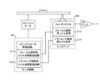
以下、本願発明を実施するための最良の形態であるコイル負荷駆動回路を説明する。このコイル負荷駆動回路1は、図1に示すように、外部から入力端子INを介して入力制御電圧VIN、入力端子REFを介して入力基準電圧VREFを入力し、その電圧差に応じたPWMパルスを第1の出力端子OUT1又は第2の出力端子OUT2を介してコイル負荷としてのモータ5の両端子間に印加することにより、モータ5を正又は負方向に、すなわち正転又は逆転方向に駆動する。ここで、モータ5は、第1の出力端子OUT1が第2の出力端子OUT2に対して正電圧ならば正転方向に、負電圧ならば逆転方向に駆動される。なお、本実施形態では回転するモータをコイル負荷として説明しているが、コイル負荷はこれに限定されず直線又は曲線運動をするもの(アクチュエータ等)でも構わない。
Hereinafter, a coil load driving circuit which is the best mode for carrying out the present invention will be described. As shown in FIG. 1, the coil load driving circuit 1 receives an input control voltage V IN from the outside via an input terminal IN and an input reference voltage V REF via an input terminal REF, and according to the voltage difference. By applying a PWM pulse between both terminals of the
さらに詳しくは、コイル負荷駆動回路1は、入力制御電圧VINと入力基準電圧VREFを入力してその差に応じ、発振器(OSC)13が出力する三角波信号TRIの中心電圧VCENを中心にして増減する第1の伝達電圧VTR1と、三角波信号TRIの中心電圧VCENを中心にして第1の伝達電圧VTR1と逆に増減する第2の伝達電圧VTR2とを出力する伝達電圧生成回路17と、第1の伝達電圧VTR1を反転入力端子、三角波信号TRIを非反転入力端子に入力し、それらを比較して第1のPWM信号PW1を出力する第1のPWMコンパレータ14と、第2の伝達電圧VTR2を反転入力端子、三角波信号TRIを非反転入力端子に入力し、それらを比較して第2のPWM信号PW2を出力する第2のPWMコンパレータ15と、第1及び第2のPWM信号PW1、PW2の排他的論理和(Exclusive OR)信号EXと第1のPWM信号PW1との論理積(AND)信号と、第1及び第2のPWM信号PW1、PW2の排他的論理和信号EXと第2のPWM信号PW2との論理積信号とを出力する出力PWMパルス合成回路16と、排他的論理和信号EXと第1のPWM信号PW1との論理積信号により制御されてモータ5の一方の端子にPWMパルスを出力する第1出力バッファ11と、排他的論理和信号EXと第2のPWM信号PW2との論理積信号により制御されてモータ5の他方の端子にPWMパルスを出力する第2の出力バッファ12と、を備える。 More specifically, the coil load driving circuit 1 receives an input reference voltage V REF and the input control voltage V IN according to the difference in, the center voltage V CEN of the triangular wave signal TRI to the oscillator (OSC) 13 is output to the center a first transfer voltage V TR1 to increase or decrease Te, transfer voltage second outputs and a transmission voltage V TR2 to increase or decrease the first transfer voltage V TR1 opposite around the center voltage V CEN of the triangular wave signal TRI generation A circuit 17 and a first PWM comparator 14 that inputs a first transmission voltage V TR1 to an inverting input terminal and a triangular wave signal TRI to a non-inverting input terminal, compares them, and outputs a first PWM signal PW1; inverting input terminal of the second transfer voltage V TR2, enter the triangular wave signal TRI to the non-inverting input terminal, the second PWM comparator which outputs a second PWM signal PW2 by comparing them Data 15, the logical product (AND) signal of the exclusive OR signal EX of the first and second PWM signals PW1 and PW2, and the first PWM signal PW1, and the first and second An output PWM pulse synthesizing circuit 16 that outputs the logical product signal of the exclusive logical sum signal EX of the PWM signals PW1 and PW2 and the second PWM signal PW2, the exclusive logical sum signal EX and the first PWM signal PW1 Of the first output buffer 11 that outputs a PWM pulse to one terminal of the motor 5 and the logical product signal of the exclusive OR signal EX and the second PWM signal PW2. 5 and a second output buffer 12 for outputting a PWM pulse to the other terminal.
伝達電圧生成回路17は、入力制御電圧VINを反転入力端子、入力基準電圧VREFを非反転入力端子に入力し、その電圧差に比例して正負両極性の電流を出力する電圧電流変換器31と、一端が電圧電流変換器31の正極性の電流を出力する端子、他端が三角波信号TRIの中心電圧VCENに接続されるバイアス用抵抗32と、一端が電圧電流変換器31の負極性の電流を出力する端子、他端が三角波信号TRIの中心電圧VCENに接続されるバイアス用抵抗33と、から構成される。そして、電圧電流変換器31の正極性の出力電流をバイアス用抵抗32に流すことによりその一端に発生する電圧が第1の伝達電圧VTR1となり、電圧電流変換器31の負極性の出力電流をバイアス用抵抗33に流すことによりその一端に発生する電圧が第2の伝達電圧VTR2となる。また、電圧電流変換器31は、入力制御電圧VINが入力基準電圧VREFよりも低いと、バイアス用抵抗32に発生する電圧(第1の伝達電圧VTR1)が中心電圧VCENを基準に正になるように正極性の電流を、バイアス用抵抗33に発生する電圧(第2の伝達電圧VTR2)が中心電圧VCENを基準に負になるように負極性の電流を出力する。逆に、入力制御電圧VINが入力基準電圧VREFよりも高いと、バイアス用抵抗32に発生する電圧(第1の伝達電圧VTR1)が中心電圧VCENを基準に負になるように正極性の電流を、バイアス用抵抗33に発生する電圧(第2の伝達電圧VTR2)が中心電圧VCENを基準に正になるように負極性の電流を出力する。
The transmission voltage generation circuit 17 inputs an input control voltage VIN to an inverting input terminal and an input reference voltage VREF to a non-inverting input terminal, and outputs a current of both positive and negative polarities in proportion to the voltage difference. 31, a terminal for outputting a positive current of the voltage-
出力PWMパルス合成回路16は、第1及び第2のPWM信号PW1、PW2の排他的論理和(Exclusive OR)信号EXを出力するEOR回路21と、排他的論理和信号EXと第1のPWM信号PW1との論理積信号を出力するAND回路22と、排他的論理和信号EXと第2のPWM信号PW2との論理積信号を出力するAND回路23と、から構成される。従って、AND回路22が出力する論理積信号は第1の出力バッファ11に入力され、AND回路23が出力する論理積信号は第2の出力バッファ12に入力される。
The output PWM
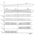
このコイル負荷駆動回路1の動作を図2の波形図に基づいて説明する。同図は入力制御電圧VINを直線的に上昇させた場合に各部に生じる波形を示したものである。(a)は入力制御電圧VIN、(b)は第1及び第2の伝達電圧VTR1、VTR2と三角波信号TRI、(c)は第1のPWM信号PW1、(d)は第2のPWM信号PW2、(e)は排他的論理和信号EX、(f)は第1の出力端子OUT1のPWMパルス、(g)は第2の出力端子OUT2のPWMパルスを示している。この波形図から明らかなように、入力制御電圧VINが入力基準電圧VREFよりも低くその差が大きい場合、第1の伝達電圧VTR1は高く、第1のPWM信号PW1のパルス幅(すなわちハイレベル期間)は小さい。一方、第2の伝達電圧VTR2は低く、第2のPWM信号PW2のパルス幅(すなわちハイレベル期間)は大きい。入力制御電圧VINが上昇していくと、第1の伝達電圧VTR1は下降して第1のPWM信号PW1のパルス幅は徐々に大きくなり、第2の伝達電圧VTR2は上昇して第2のPWM信号PW2のパルス幅は徐々に小さくなる。 The operation of the coil load drive circuit 1 will be described based on the waveform diagram of FIG. This figure shows waveforms generated in each part when the input control voltage VIN is linearly increased. (A) is the input control voltage V IN , (b) is the first and second transmission voltages V TR1 and V TR2 and the triangular wave signal TRI, (c) is the first PWM signal PW1, (d) is the second The PWM signal PW2, (e) shows the exclusive OR signal EX, (f) shows the PWM pulse at the first output terminal OUT1, and (g) shows the PWM pulse at the second output terminal OUT2. As is apparent from this waveform diagram, when the input control voltage VIN is lower than the input reference voltage VREF and the difference is large, the first transmission voltage VTR1 is high and the pulse width of the first PWM signal PW1 (ie, High level period) is small. On the other hand, the second transmission voltage VTR2 is low, and the pulse width (that is, the high level period) of the second PWM signal PW2 is large. As the input control voltage VIN increases, the first transmission voltage V TR1 decreases and the pulse width of the first PWM signal PW1 gradually increases, and the second transmission voltage V TR2 increases and increases. The pulse width of the second PWM signal PW2 gradually decreases.
排他的論理和信号EXは、入力制御電圧VINが入力基準電圧VREFよりも低い場合、入力制御電圧VINが上昇するに従いパルス幅は徐々に小さくなる。入力制御電圧VINが入力基準電圧VREFに等しくなったとき、第1及び第2のPWM信号PW1、PW2のパルス幅は共にデューティ比50%となって一致するので、そのパルス幅は0になる。そして、入力制御電圧VINが入力基準電圧VREFよりも高い場合、入力制御電圧VINが上昇するに従いパルス幅は徐々に大きくなる。 When the input control voltage VIN is lower than the input reference voltage VREF , the exclusive OR signal EX has a pulse width that gradually decreases as the input control voltage VIN increases. When the input control voltage VIN becomes equal to the input reference voltage V REF , the pulse widths of the first and second PWM signals PW1 and PW2 coincide with each other with a duty ratio of 50%. Become. When the input control voltage VIN is higher than the input reference voltage VREF , the pulse width gradually increases as the input control voltage VIN increases.
また、第1及び第2の出力端子OUT1、OUT2には、第1及び第2のPWM信号PW1、PW2のうちパルス幅が大きい側にだけPWMパルスが出力される。すなわち、入力制御電圧VINが入力基準電圧VREFよりも低い場合は、第2の出力端子OUT2からPWMパルスが出力され、かつ第1の出力端子OUT1はPWMパルスが出力されないので接地電位に固定される。このとき、モータ5は逆方向に回転する。入力制御電圧VINが入力基準電圧VREFよりも高い場合は、第1の出力端子OUT1からPWMパルスが出力され、かつ第2の出力端子OUT2は接地電位に固定される。このとき、モータ5は正方向に回転する。そして、入力制御電圧VINが入力基準電圧VREFに等しいときは、第1及び第2の出力端子OUT1、OUT2は共に接地電位に固定され、モータ5は静止する。なお、入力制御電圧VINと入力基準電圧VREFの差が大きくなるに従って、第1の出力端子OUT1又は第2の出力端子OUT2から出力されるPWMパルスのパルス幅が大きくなりモータ5を駆動するトルクは大きくなる。
Also, PWM pulses are output to the first and second output terminals OUT1 and OUT2 only on the side of the first and second PWM signals PW1 and PW2 having the larger pulse width. That is, when the input control voltage V IN is lower than the input reference voltage V REF , the PWM pulse is output from the second output terminal OUT2, and the first output terminal OUT1 is fixed to the ground potential because the PWM pulse is not output. Is done. At this time, the
このように、このコイル負荷駆動回路1は、入力制御電圧VINと入力基準電圧VREFとの差に従い、単調性及び線形性を維持して増減する第1の伝達電圧VTR1に対応する第1のPWM信号PW1と、単調性及び線形性を維持して増減する第2の伝達電圧VTR2に対応する第2のPWM信号PW2と、の排他的論理和、すなわち差の絶対値がPWMパルスとしてモータ5の一方又は他方のいずれかの端子にだけ出力される。このコイル負荷駆動回路1は、入力制御電圧VINと入力基準電圧VREFが等しくなる付近で単調性又は線形性が崩れることはなく、コイル負荷駆動回路201と同様に、図13(a)、(b)の特性図に示すような入出力の特性を得ることができるうえに、入力制御電圧VINと入力基準電圧VREFが等しい、すなわちモータ5が静止している状態では、第1及び第2の出力端子OUT1、OUT2は共に接地電位に固定され、PWMパルスを出力しないので、第1及び第2の出力バッファ11、12のスイッチングにより発生する輻射ノイズを抑制することが可能になる。
As described above, the coil load driving circuit 1 corresponds to the first transmission voltage V TR1 corresponding to the first transmission voltage V TR1 that increases and decreases while maintaining monotonicity and linearity according to the difference between the input control voltage VIN and the input reference voltage VREF . 1 of the PWM signal PW1 and the second PWM signal PW2 corresponding to the second transmission voltage VTR2 that increases or decreases while maintaining monotonicity and linearity, that is, the absolute value of the difference is the PWM pulse. Is output only to one of the terminals of the
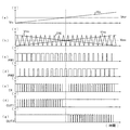
次に、本発明の別の実施形態であるコイル負荷駆動回路を説明する。このコイル負荷駆動回路2は、図3の回路図に示すように、コイル負荷駆動回路1における伝達電圧生成回路17を伝達電圧生成回路27に換え、また、三角波信号TRIの中心電圧VCENを入力基準電圧VREFに一致させたものである。この伝達電圧生成回路27は、入力端子INの入力制御電圧VINを入力端子REFの入力基準電圧VREFを基準に反転出力する第1の反転アンプ33とその出力を更に反転出力する第2の反転アンプ34とを備える。そして、第1の反転アンプ33の出力が第1の伝達電圧VTR1、第2の反転アンプ34の出力が第2の伝達電圧VTR2となる。コイル負荷駆動回路2の動作は前述の図2と同様の波形となる。このコイル負荷駆動回路2は、中心電圧VCENを入力基準電圧VREFに一致させて三角波信号TRIを発生させる必要があるが、電圧電流変換器に比べて回路規模の小さな2個の反転アンプ33、34を用いているので全体の回路規模の縮小を図ることができる。
Next, a coil load drive circuit according to another embodiment of the present invention will be described. As shown in the circuit diagram of FIG. 3, the coil load drive circuit 2 replaces the transmission voltage generation circuit 17 in the coil load drive circuit 1 with a transmission voltage generation circuit 27, and receives the center voltage V CEN of the triangular wave signal TRI. It is made to coincide with the reference voltage VREF . The transmission voltage generating circuit 27 includes a
なお、以上説明したコイル負荷駆動回路1及び2は、第1の出力端子OUT1又は第2の出力端子OUT2から出力されるPWMパルスのパルス期間(ハイレベル期間)にモータ5の両端子間に電圧が印加され、その電圧の方向に電流が流れる。パルス期間でない期間(ローレベル期間)にはモータ5の両端子は接地電位に固定されているのでモータ5の両端子間には電圧は印加されないが、この期間にはモータ5の誘導性の性質によって電流が流れ続けようとするため、いわゆる回生電流が流れる。図4に示すように、第1及び第2の出力バッファ11、12の電源電圧VCC側の出力トランジスタ11a、12aがP型MOSトランジスタ、接地電位側の出力トランジスタ11b、12bがN型MOSトランジスタである場合、第1の出力端子OUT1からPWMパルスが出力されているとき、パルス期間でない期間(ローレベル期間)には第1の出力バッファ11の出力トランジスタ11bからモータ5を通って第2の出力バッファ12の出力トランジスタ12bに回生電流I1が流れる。一般に、N型MOSトランジスタはP型MOSトランジスタよりもオン抵抗は小さいので、N型MOSトランジスタに回生電流を流すようにするとP型MOSトランジスタの場合よりも電力消費は少なくなる。従って、コイル負荷駆動回路1及び2は、N型MOSトランジスタとP型MOSトランジスタの両方に回生電流が流れる場合がある上記コイル負荷駆動回路201に比べると、電力消費の面でも有利になる。N型MOSトランジスタをNPN型バイポーラトランジスタ、P型MOSトランジスタをPNP型バイポーラトランジスタに置き換えた構成である場合も同様である。
Note that the coil load drive circuits 1 and 2 described above have a voltage between both terminals of the
よって、コイル負荷駆動回路1及び2のように、第1の出力端子OUT1又は第2の出力端子OUT2からの出力のうち固定される電位は接地電位とするのが望ましいが、これを電源電圧VCCとするように変形することも可能である。以下、本発明の更に別の実施形態としてこれを説明する。図5の回路図に示すコイル負荷駆動回路3は、コイル負荷駆動回路1における第1及び第2のPWMコンパレータ14、15の入力端子の極性を互いに換え、出力PWMパルス合成回路16をAND回路22、23の出力を反転するインバータ31、32を追加した出力PWMパルス合成回路26に換えたものである。このコイル負荷駆動回路3では、図6の波形図に示すように、第1の出力端子OUT1から出力されるPWMパルスのパルス幅は、入力制御電圧VINを直線的に上昇させると徐々に大きくなり、入力制御電圧VINが入力基準電圧VREFに等しいかそれよりも高いと電源電圧VCCに固定される。一方、第2の出力端子OUT2から出力されるPWMパルスのパルス幅は、入力制御電圧VINを直線的に上昇させた場合、入力制御電圧VINが入力基準電圧VREFよりも低いか等しいと電源電圧VCCに固定され、入力制御電圧VINが入力基準電圧VREFよりも高いところで徐々に小さくなる。コイル負荷駆動回路3は、コイル負荷駆動回路1と同様に、モータ5が静止している状態で第1及び第2の出力バッファ11、12のスイッチングにより発生する輻射ノイズを抑制することが可能になる。また、コイル負荷駆動回路2も同様にして変形することができる。
Therefore, as in the coil load driving circuits 1 and 2, it is desirable that the fixed potential among the outputs from the first output terminal OUT1 or the second output terminal OUT2 is the ground potential. It is also possible to modify it to be CC . Hereinafter, this will be described as still another embodiment of the present invention. The coil load drive circuit 3 shown in the circuit diagram of FIG. 5 changes the polarities of the input terminals of the first and
このように、以上説明した本発明の実施形態であるコイル負荷駆動回路は輻射ノイズの発生を抑制することが可能となる。また、このコイル負荷駆動回路と、それにより駆動され、フォーカス調整やトラッキング調整などを行うコイル負荷と、を備える光ディスク装置は、輻射ノイズが抑制されているので、安定した動作を行うことができる。 As described above, the coil load driving circuit according to the embodiment of the present invention described above can suppress the generation of radiation noise. In addition, an optical disc apparatus including this coil load drive circuit and a coil load that is driven thereby to perform focus adjustment, tracking adjustment, and the like can perform stable operation because radiation noise is suppressed.
なお、本発明は、実施形態に記載したものに限られることなく、特許請求の範囲に記載した事項の範囲内でのさまざまな設計変更が可能である。例えば、コイル負荷駆動回路1の電圧電流変換器17と第1及び第2のPWMコンパレータ14、15の入力端子の極性を同時に換えても同様の動作が可能である。また、出力PWMパルス合成回路16(又は26)は、同様の出力を合成するのに様々な論理回路構成が可能であるのは勿論である。
The present invention is not limited to that described in the embodiments, and various design changes can be made within the scope of the matters described in the claims. For example, the same operation is possible even if the polarities of the voltage-current converter 17 of the coil load drive circuit 1 and the input terminals of the first and
1、2、3 コイル負荷駆動回路
5 モータ
11 第1の出力バッファ
12 第2の出力バッファ
13 発振器
14 第1のPWMコンパレータ
15 第2のPWMコンパレータ
16 出力PWMパルス合成回路
17 伝達電圧生成回路
21 EOR回路
VIN 入力制御電圧
VREF 入力基準電圧
VTR1 第1の伝達電圧
VTR2 第2の伝達電圧
TRI 三角波信号
VCEN 三角波信号TRIの中心電圧
PW1 第1のPWM信号
PW2 第2のPWM信号
EX 第1及び第2のPWM信号の排他的論理和信号
1, 2, 3 Coil load drive circuit
DESCRIPTION OF
Claims (5)
前記入力制御電圧と前記入力基準電圧を入力してその差に応じ、発振器が出力する三角波信号の中心電圧を中心にして増減する第1の伝達電圧と、発振器が出力する三角波信号の中心電圧を中心にして第1の伝達電圧と逆に増減する第2の伝達電圧と、を出力する伝達電圧生成回路と、
第1の伝達電圧を前記三角波信号と比較して第1のPWM信号を出力する第1のPWMコンパレータと、
第2の伝達電圧を前記三角波信号と比較して第2のPWM信号を出力する第2のPWMコンパレータと、
第1及び第2のPWM信号の排他的論理和信号と第1のPWM信号との論理積信号と、第1及び第2のPWM信号の排他的論理和信号と第2のPWM信号との論理積信号とを出力する出力PWMパルス合成回路と、
前記排他的論理和信号と第1のPWM信号との論理積信号により制御されてコイル負荷の一方の端子にPWMパルスを出力する第1の出力バッファと、
前記排他的論理和信号と第2のPWM信号との論理積信号により制御されてコイル負荷の他方の端子にPWMパルスを出力する第2の出力バッファと、
を備えてなることを特徴とするコイル負荷駆動回路。 A coil load driving circuit that drives a coil load in a positive or negative direction by applying a PWM pulse according to a difference between an input control voltage and an input reference voltage between both terminals of the coil load,
According to the difference between the input control voltage and the input reference voltage, a first transmission voltage that increases or decreases around the center voltage of the triangular wave signal output from the oscillator, and the center voltage of the triangular wave signal output from the oscillator A transmission voltage generation circuit that outputs a second transmission voltage that increases or decreases in reverse to the first transmission voltage at the center;
A first PWM comparator that compares a first transmission voltage with the triangular wave signal and outputs a first PWM signal;
A second PWM comparator for comparing a second transmission voltage with the triangular wave signal and outputting a second PWM signal;
The logical product of the exclusive logical sum signal of the first and second PWM signals and the first PWM signal, and the logical sum of the exclusive logical sum signal of the first and second PWM signals and the second PWM signal. An output PWM pulse synthesis circuit that outputs a product signal;
A first output buffer controlled by a logical product signal of the exclusive OR signal and the first PWM signal to output a PWM pulse to one terminal of the coil load;
A second output buffer controlled by a logical product signal of the exclusive OR signal and the second PWM signal to output a PWM pulse to the other terminal of the coil load;
A coil load drive circuit comprising:
前記伝達電圧生成回路は、前記入力制御電圧と前記入力基準電圧の差に比例して正負両極性の電流を出力する電圧電流変換器と、一端が電圧電流変換器のそれぞれの出力、他端が前記三角波信号の中心電圧に接続された2個のバイアス用抵抗と、を備え、
バイアス用抵抗のそれぞれの一端に発生する電圧を第1又は第2の伝達電圧とすることを特徴とするコイル負荷駆動回路。 In the coil load drive circuit according to claim 1,
The transmission voltage generation circuit includes a voltage-current converter that outputs a positive and negative current in proportion to the difference between the input control voltage and the input reference voltage, one end of each output of the voltage-current converter, and the other end Two biasing resistors connected to the center voltage of the triangular wave signal,
A coil load driving circuit characterized in that a voltage generated at one end of each of the bias resistors is the first or second transmission voltage.
前記伝達電圧生成回路は、前記入力制御電圧を前記入力基準電圧を基準に反転出力する第1の反転アンプと、その出力を更に反転出力する第2の反転アンプと、を備え、
前記三角波信号の中心電圧を前記入力基準電圧に一致させ、第1の反転アンプの出力を第1の伝達電圧、第2の反転アンプの出力を第2の伝達電圧とすることを特徴とするコイル負荷駆動回路。 In the coil load drive circuit according to claim 1,
The transmission voltage generation circuit includes a first inverting amplifier that inverts and outputs the input control voltage with reference to the input reference voltage, and a second inverting amplifier that further inverts and outputs the output.
A coil characterized in that a center voltage of the triangular wave signal is matched with the input reference voltage, an output of the first inverting amplifier is a first transmission voltage, and an output of the second inverting amplifier is a second transmission voltage. Load drive circuit.
PWMパルスのパルス期間でない期間にはモータの両端子に接地電位を出力することを特徴とするコイル負荷駆動回路。 In the coil load drive circuit according to any one of claims 1 to 3,
A coil load driving circuit which outputs a ground potential to both terminals of a motor during a period other than a pulse period of a PWM pulse.
コイル負荷駆動回路により駆動され、フォーカス調整又はトラッキング調整を行うコイル負荷と、
を備えてなることを特徴とする光ディスク装置。
A coil load drive circuit according to any one of claims 1 to 4,
A coil load driven by a coil load drive circuit for focus adjustment or tracking adjustment; and
An optical disc apparatus comprising:
Priority Applications (6)
| Application Number | Priority Date | Filing Date | Title |
|---|---|---|---|
| JP2004158319A JP3969590B2 (en) | 2004-05-27 | 2004-05-27 | Coil load driving circuit and optical disk apparatus |
| KR1020067024759A KR101113521B1 (en) | 2004-05-27 | 2005-05-26 | Coil load driving circuit and optical disc device |
| CNB2005800169625A CN100521500C (en) | 2004-05-27 | 2005-05-26 | Coil load driving circuit and optical disc device |
| PCT/JP2005/009608 WO2005117250A1 (en) | 2004-05-27 | 2005-05-26 | Coil load driving circuit and optical disc device |
| US11/569,638 US7630616B2 (en) | 2004-05-27 | 2005-05-26 | Coil load driving circuit and optical disc device |
| TW094117490A TW200607222A (en) | 2004-05-27 | 2005-05-27 | Coil load drive circuit and optical disk device |
Applications Claiming Priority (1)
| Application Number | Priority Date | Filing Date | Title |
|---|---|---|---|
| JP2004158319A JP3969590B2 (en) | 2004-05-27 | 2004-05-27 | Coil load driving circuit and optical disk apparatus |
Publications (2)
| Publication Number | Publication Date |
|---|---|
| JP2005341736A JP2005341736A (en) | 2005-12-08 |
| JP3969590B2 true JP3969590B2 (en) | 2007-09-05 |
Family
ID=35451204
Family Applications (1)
| Application Number | Title | Priority Date | Filing Date |
|---|---|---|---|
| JP2004158319A Expired - Fee Related JP3969590B2 (en) | 2004-05-27 | 2004-05-27 | Coil load driving circuit and optical disk apparatus |
Country Status (6)
| Country | Link |
|---|---|
| US (1) | US7630616B2 (en) |
| JP (1) | JP3969590B2 (en) |
| KR (1) | KR101113521B1 (en) |
| CN (1) | CN100521500C (en) |
| TW (1) | TW200607222A (en) |
| WO (1) | WO2005117250A1 (en) |
Families Citing this family (5)
| Publication number | Priority date | Publication date | Assignee | Title |
|---|---|---|---|---|
| WO2008004322A1 (en) * | 2006-07-07 | 2008-01-10 | Panasonic Corporation | Brushless motor drive circuit and motor having the same |
| JP2010003147A (en) * | 2008-06-20 | 2010-01-07 | Fujitsu Ltd | Temperature control apparatus and optical transmission device |
| KR101919400B1 (en) | 2012-07-12 | 2018-11-19 | 삼성전자 주식회사 | Motor driving signal generation system and method thereof, semiconductor device, electronic device and method for controlling vibration thereof |
| WO2023173241A1 (en) * | 2022-03-14 | 2023-09-21 | 深圳市汇顶科技股份有限公司 | Class-d amplifier, and related chip and electronic device |
| CN114421906B (en) * | 2022-03-14 | 2023-05-02 | 深圳市汇顶科技股份有限公司 | Class D amplifier, related chip and electronic device |
Family Cites Families (11)
| Publication number | Priority date | Publication date | Assignee | Title |
|---|---|---|---|---|
| US4153853A (en) * | 1976-07-07 | 1979-05-08 | Villeneuve Dail A De | DC motor speed controller |
| JPS608541B2 (en) * | 1976-09-28 | 1985-03-04 | ソニー株式会社 | reel control device |
| IT1156505B (en) * | 1982-09-01 | 1987-02-04 | Olivetti & Co Spa | DEVICE TO CONTROL THE SPEED AND POSITIONING OF AN ELECTRIC MOTOR |
| US4772994A (en) * | 1987-09-10 | 1988-09-20 | Nishimu Electronics Industries, Co., Ltd. | Power source using high-frequency phase control |
| JP3446220B2 (en) * | 1992-05-21 | 2003-09-16 | ソニー株式会社 | Motor drive |
| US5450521A (en) * | 1994-08-03 | 1995-09-12 | Sunpower, Inc. | Pulse width modulator |
| JP3723369B2 (en) | 1999-02-19 | 2005-12-07 | 富士通株式会社 | Motor drive device adjustment method, motor drive device, and information storage device |
| JP3786170B2 (en) | 1999-11-26 | 2006-06-14 | ローム株式会社 | Inductive load drive circuit |
| JP2003164194A (en) | 2001-11-21 | 2003-06-06 | Sharp Corp | Dc motor drive device in ink-jet recording device |
| US6819011B2 (en) * | 2002-11-14 | 2004-11-16 | Fyre Storm, Inc. | Switching power converter controller with watchdog timer |
| TW200814533A (en) * | 2006-09-11 | 2008-03-16 | Beyond Innovation Tech Co Ltd | Apparatus for pulse width modulation and circuit and method for controlling thereof |
-
2004
- 2004-05-27 JP JP2004158319A patent/JP3969590B2/en not_active Expired - Fee Related
-
2005
- 2005-05-26 US US11/569,638 patent/US7630616B2/en not_active Expired - Fee Related
- 2005-05-26 WO PCT/JP2005/009608 patent/WO2005117250A1/en active Application Filing
- 2005-05-26 CN CNB2005800169625A patent/CN100521500C/en not_active Expired - Fee Related
- 2005-05-26 KR KR1020067024759A patent/KR101113521B1/en not_active IP Right Cessation
- 2005-05-27 TW TW094117490A patent/TW200607222A/en not_active IP Right Cessation
Also Published As
| Publication number | Publication date |
|---|---|
| KR20070021222A (en) | 2007-02-22 |
| CN100521500C (en) | 2009-07-29 |
| JP2005341736A (en) | 2005-12-08 |
| KR101113521B1 (en) | 2012-03-13 |
| CN1957525A (en) | 2007-05-02 |
| TWI363484B (en) | 2012-05-01 |
| US20080019678A1 (en) | 2008-01-24 |
| TW200607222A (en) | 2006-02-16 |
| US7630616B2 (en) | 2009-12-08 |
| WO2005117250A1 (en) | 2005-12-08 |
Similar Documents
| Publication | Publication Date | Title |
|---|---|---|
| KR100972686B1 (en) | Motor drive device and electric equipment using this | |
| US7151394B2 (en) | Phase shifting and PWM driving circuits and methods | |
| JP4793294B2 (en) | Digital input class D amplifier | |
| US20080265822A1 (en) | Class G motor drive | |
| US20060049785A1 (en) | Brushless motor drive device | |
| JP5908224B2 (en) | H bridge drive circuit | |
| JP2012147552A (en) | Dc-dc converter | |
| KR101113521B1 (en) | Coil load driving circuit and optical disc device | |
| US7542262B2 (en) | Apparatus for driving an electromagnetic load | |
| JP2002218783A (en) | Motor driver | |
| JP4461842B2 (en) | Switching regulator and switching regulator control method | |
| JP4705264B2 (en) | Switching regulator | |
| JP3942583B2 (en) | Driver circuit | |
| JP4850344B2 (en) | DC-DC converter control circuit and DC-DC converter | |
| JP3813045B2 (en) | H-bridge driver | |
| TW200814516A (en) | Class-D audio amplifier with half-swing pulse-width-modulation | |
| JP4423464B2 (en) | Level shift circuit, synchronous rectification type DC / DC converter, and step-up / down chopper type DC / DC converter | |
| US20100253316A1 (en) | Current control circuit | |
| US8207695B2 (en) | Control circuit of a full-bridge stage | |
| JP2008301192A (en) | Pwm drive circuit and driving method | |
| KR100796319B1 (en) | Class-d audio amplifier with half-swing pulse-width-modulation | |
| JP5918512B2 (en) | H-type bridge circuit and motor drive device | |
| JP2004056211A (en) | Semiconductor device and class-d amplifier | |
| JP4653496B2 (en) | Actuator drive circuit | |
| JP2006006016A (en) | Pulse width modulation drive circuit |
Legal Events
| Date | Code | Title | Description |
|---|---|---|---|
| TRDD | Decision of grant or rejection written | ||
| A01 | Written decision to grant a patent or to grant a registration (utility model) |
Free format text: JAPANESE INTERMEDIATE CODE: A01 Effective date: 20070531 |
|
| A61 | First payment of annual fees (during grant procedure) |
Free format text: JAPANESE INTERMEDIATE CODE: A61 Effective date: 20070531 |
|
| R150 | Certificate of patent or registration of utility model |
Free format text: JAPANESE INTERMEDIATE CODE: R150 Ref document number: 3969590 Country of ref document: JP Free format text: JAPANESE INTERMEDIATE CODE: R150 |
|
| FPAY | Renewal fee payment (event date is renewal date of database) |
Free format text: PAYMENT UNTIL: 20110615 Year of fee payment: 4 |
|
| FPAY | Renewal fee payment (event date is renewal date of database) |
Free format text: PAYMENT UNTIL: 20120615 Year of fee payment: 5 |
|
| FPAY | Renewal fee payment (event date is renewal date of database) |
Free format text: PAYMENT UNTIL: 20130615 Year of fee payment: 6 |
|
| R250 | Receipt of annual fees |
Free format text: JAPANESE INTERMEDIATE CODE: R250 |
|
| R250 | Receipt of annual fees |
Free format text: JAPANESE INTERMEDIATE CODE: R250 |
|
| LAPS | Cancellation because of no payment of annual fees |