JP2019512995A - Battery management system with adiabatic switched capacitor circuit - Google Patents
Battery management system with adiabatic switched capacitor circuit Download PDFInfo
- Publication number
- JP2019512995A JP2019512995A JP2018546812A JP2018546812A JP2019512995A JP 2019512995 A JP2019512995 A JP 2019512995A JP 2018546812 A JP2018546812 A JP 2018546812A JP 2018546812 A JP2018546812 A JP 2018546812A JP 2019512995 A JP2019512995 A JP 2019512995A
- Authority
- JP
- Japan
- Prior art keywords
- converter
- switched capacitor
- battery
- capacitor network
- line
- Prior art date
- Legal status (The legal status is an assumption and is not a legal conclusion. Google has not performed a legal analysis and makes no representation as to the accuracy of the status listed.)
- Pending
Links
Images


Classifications
-
- H—ELECTRICITY
- H02—GENERATION; CONVERSION OR DISTRIBUTION OF ELECTRIC POWER
- H02J—CIRCUIT ARRANGEMENTS OR SYSTEMS FOR SUPPLYING OR DISTRIBUTING ELECTRIC POWER; SYSTEMS FOR STORING ELECTRIC ENERGY
- H02J3/00—Circuit arrangements for ac mains or ac distribution networks
- H02J3/18—Arrangements for adjusting, eliminating or compensating reactive power in networks
-
- H—ELECTRICITY
- H02—GENERATION; CONVERSION OR DISTRIBUTION OF ELECTRIC POWER
- H02J—CIRCUIT ARRANGEMENTS OR SYSTEMS FOR SUPPLYING OR DISTRIBUTING ELECTRIC POWER; SYSTEMS FOR STORING ELECTRIC ENERGY
- H02J7/00—Circuit arrangements for charging or depolarising batteries or for supplying loads from batteries
- H02J7/007—Regulation of charging or discharging current or voltage
- H02J7/00712—Regulation of charging or discharging current or voltage the cycle being controlled or terminated in response to electric parameters
- H02J7/007182—Regulation of charging or discharging current or voltage the cycle being controlled or terminated in response to electric parameters in response to battery voltage
-
- H—ELECTRICITY
- H02—GENERATION; CONVERSION OR DISTRIBUTION OF ELECTRIC POWER
- H02J—CIRCUIT ARRANGEMENTS OR SYSTEMS FOR SUPPLYING OR DISTRIBUTING ELECTRIC POWER; SYSTEMS FOR STORING ELECTRIC ENERGY
- H02J7/00—Circuit arrangements for charging or depolarising batteries or for supplying loads from batteries
- H02J7/02—Circuit arrangements for charging or depolarising batteries or for supplying loads from batteries for charging batteries from ac mains by converters
- H02J7/04—Regulation of charging current or voltage
-
- H—ELECTRICITY
- H02—GENERATION; CONVERSION OR DISTRIBUTION OF ELECTRIC POWER
- H02M—APPARATUS FOR CONVERSION BETWEEN AC AND AC, BETWEEN AC AND DC, OR BETWEEN DC AND DC, AND FOR USE WITH MAINS OR SIMILAR POWER SUPPLY SYSTEMS; CONVERSION OF DC OR AC INPUT POWER INTO SURGE OUTPUT POWER; CONTROL OR REGULATION THEREOF
- H02M3/00—Conversion of dc power input into dc power output
- H02M3/02—Conversion of dc power input into dc power output without intermediate conversion into ac
- H02M3/04—Conversion of dc power input into dc power output without intermediate conversion into ac by static converters
- H02M3/06—Conversion of dc power input into dc power output without intermediate conversion into ac by static converters using resistors or capacitors, e.g. potential divider
- H02M3/07—Conversion of dc power input into dc power output without intermediate conversion into ac by static converters using resistors or capacitors, e.g. potential divider using capacitors charged and discharged alternately by semiconductor devices with control electrode, e.g. charge pumps
- H02M3/073—Charge pumps of the Schenkel-type
-
- H—ELECTRICITY
- H02—GENERATION; CONVERSION OR DISTRIBUTION OF ELECTRIC POWER
- H02M—APPARATUS FOR CONVERSION BETWEEN AC AND AC, BETWEEN AC AND DC, OR BETWEEN DC AND DC, AND FOR USE WITH MAINS OR SIMILAR POWER SUPPLY SYSTEMS; CONVERSION OF DC OR AC INPUT POWER INTO SURGE OUTPUT POWER; CONTROL OR REGULATION THEREOF
- H02M3/00—Conversion of dc power input into dc power output
- H02M3/02—Conversion of dc power input into dc power output without intermediate conversion into ac
- H02M3/04—Conversion of dc power input into dc power output without intermediate conversion into ac by static converters
- H02M3/10—Conversion of dc power input into dc power output without intermediate conversion into ac by static converters using discharge tubes with control electrode or semiconductor devices with control electrode
- H02M3/145—Conversion of dc power input into dc power output without intermediate conversion into ac by static converters using discharge tubes with control electrode or semiconductor devices with control electrode using devices of a triode or transistor type requiring continuous application of a control signal
- H02M3/155—Conversion of dc power input into dc power output without intermediate conversion into ac by static converters using discharge tubes with control electrode or semiconductor devices with control electrode using devices of a triode or transistor type requiring continuous application of a control signal using semiconductor devices only
- H02M3/156—Conversion of dc power input into dc power output without intermediate conversion into ac by static converters using discharge tubes with control electrode or semiconductor devices with control electrode using devices of a triode or transistor type requiring continuous application of a control signal using semiconductor devices only with automatic control of output voltage or current, e.g. switching regulators
- H02M3/158—Conversion of dc power input into dc power output without intermediate conversion into ac by static converters using discharge tubes with control electrode or semiconductor devices with control electrode using devices of a triode or transistor type requiring continuous application of a control signal using semiconductor devices only with automatic control of output voltage or current, e.g. switching regulators including plural semiconductor devices as final control devices for a single load
-
- H—ELECTRICITY
- H02—GENERATION; CONVERSION OR DISTRIBUTION OF ELECTRIC POWER
- H02M—APPARATUS FOR CONVERSION BETWEEN AC AND AC, BETWEEN AC AND DC, OR BETWEEN DC AND DC, AND FOR USE WITH MAINS OR SIMILAR POWER SUPPLY SYSTEMS; CONVERSION OF DC OR AC INPUT POWER INTO SURGE OUTPUT POWER; CONTROL OR REGULATION THEREOF
- H02M3/00—Conversion of dc power input into dc power output
- H02M3/22—Conversion of dc power input into dc power output with intermediate conversion into ac
- H02M3/24—Conversion of dc power input into dc power output with intermediate conversion into ac by static converters
- H02M3/28—Conversion of dc power input into dc power output with intermediate conversion into ac by static converters using discharge tubes with control electrode or semiconductor devices with control electrode to produce the intermediate ac
- H02M3/325—Conversion of dc power input into dc power output with intermediate conversion into ac by static converters using discharge tubes with control electrode or semiconductor devices with control electrode to produce the intermediate ac using devices of a triode or a transistor type requiring continuous application of a control signal
- H02M3/335—Conversion of dc power input into dc power output with intermediate conversion into ac by static converters using discharge tubes with control electrode or semiconductor devices with control electrode to produce the intermediate ac using devices of a triode or a transistor type requiring continuous application of a control signal using semiconductor devices only
-
- H—ELECTRICITY
- H02—GENERATION; CONVERSION OR DISTRIBUTION OF ELECTRIC POWER
- H02J—CIRCUIT ARRANGEMENTS OR SYSTEMS FOR SUPPLYING OR DISTRIBUTING ELECTRIC POWER; SYSTEMS FOR STORING ELECTRIC ENERGY
- H02J2207/00—Indexing scheme relating to details of circuit arrangements for charging or depolarising batteries or for supplying loads from batteries
- H02J2207/20—Charging or discharging characterised by the power electronics converter
-
- H—ELECTRICITY
- H02—GENERATION; CONVERSION OR DISTRIBUTION OF ELECTRIC POWER
- H02M—APPARATUS FOR CONVERSION BETWEEN AC AND AC, BETWEEN AC AND DC, OR BETWEEN DC AND DC, AND FOR USE WITH MAINS OR SIMILAR POWER SUPPLY SYSTEMS; CONVERSION OF DC OR AC INPUT POWER INTO SURGE OUTPUT POWER; CONTROL OR REGULATION THEREOF
- H02M1/00—Details of apparatus for conversion
- H02M1/0067—Converter structures employing plural converter units, other than for parallel operation of the units on a single load
- H02M1/007—Plural converter units in cascade
-
- Y—GENERAL TAGGING OF NEW TECHNOLOGICAL DEVELOPMENTS; GENERAL TAGGING OF CROSS-SECTIONAL TECHNOLOGIES SPANNING OVER SEVERAL SECTIONS OF THE IPC; TECHNICAL SUBJECTS COVERED BY FORMER USPC CROSS-REFERENCE ART COLLECTIONS [XRACs] AND DIGESTS
- Y02—TECHNOLOGIES OR APPLICATIONS FOR MITIGATION OR ADAPTATION AGAINST CLIMATE CHANGE
- Y02E—REDUCTION OF GREENHOUSE GAS [GHG] EMISSIONS, RELATED TO ENERGY GENERATION, TRANSMISSION OR DISTRIBUTION
- Y02E40/00—Technologies for an efficient electrical power generation, transmission or distribution
- Y02E40/30—Reactive power compensation
Abstract
バッテリから負荷に電力供給することと別の電力源から負荷に電力供給することとの間で切り替えるための装置は、バッテリマネージャ及びスイッチドキャパシタネットワークを含み、スイッチドキャパシタネットワークは、複数のキャパシタ、第1及び第2のスイッチセット、及びコントローラを備え、コントローラは、スイッチドキャパシタネットワークを第1の状態と第2の状態との間で移行させる。An apparatus for switching between powering a load from a battery and powering a load from another power source includes a battery manager and a switched capacitor network, the switched capacitor network comprising a plurality of capacitors, A controller comprises a first and a second set of switches and a controller, and the controller transitions the switched capacitor network between a first state and a second state.
Description
関連出願
本出願は、米国仮出願第62/306,749号の優先日2016年3月11日の便益を主張するものであり、その内容は、参照により本明細書に組み込まれる。
RELATED APPLICATIONS This application claims the benefit of priority date March 11, 2016 of US Provisional Application No. 62 / 306,749, the contents of which are incorporated herein by reference.
本発明は、電力変換に関し、特にスイッチドキャパシタを使用するバッテリマネージャに関する。 The present invention relates to power conversion, and more particularly to a battery manager using switched capacitors.
多くの携帯用電気デバイスは、デバイスが、AC電源に差し込まれている間ずっと使用される。この時間中、バッテリマネージャは、必要ならばバッテリを充電するためにも、デバイスそれ自体を動作させるためにも、電力を提供しなければならない。AC電源が、切り離されるとき、バッテリマネージャは、バッテリが、電力をデバイスに提供するように、切り替えなければならない。 Many portable electrical devices are used while the device is plugged into AC power. During this time, the battery manager must provide power to both charge the battery if necessary and to operate the device itself. When AC power is disconnected, the battery manager has to switch so that the battery provides power to the device.
一態様では、本発明は、バッテリから負荷に電力供給することとAC電源から負荷に電力供給することとの間で切り替えるための装置を特徴とする。そのような装置は、その入力に接続されるAC/DCコンバータを有するバッテリマネージャを含む。AC/DCコンバータ又はバッテリマネージャのどちらかは、断熱的スイッチドキャパシタネットワークを含む。そのようなネットワークは、電荷がその上に蓄積されるキャパシタ、及び少なくとも一部にはインダクタンスを通って電荷を通過させる結果としての電荷の変化率を制約するための回路を有することによって特徴付けられる。 In one aspect, the invention features an apparatus for switching between powering a load from a battery and powering from an AC power source. Such devices include a battery manager having an AC / DC converter connected to its input. Either the AC / DC converter or the battery manager comprises an adiabatic switched capacitor network. Such networks are characterized by having a capacitor on which the charge is stored, and at least in part by a circuit for limiting the rate of change of the charge as a result of passing the charge through the inductance. .
別の態様では、本発明は、バッテリに蓄積されるエネルギーを使用して負荷に電力供給することとAC電源からのエネルギーを使用して負荷に電力供給することとの間で切り替えるための装置を特徴とし、本装置は、バッテリマネージャと、スイッチドキャパシタネットワークと、負荷が、AC電源からのエネルギーを使用して電力供給されている間にバッテリを充電するためのバッテリ充電器と、第1のコントローラとを備え、バッテリマネージャは、ブリッジ整流器に結合するための入力端子を備え、スイッチドキャパシタネットワークは、複数のキャパシタ並びに第1及び第2のスイッチセットを備え、第1のスイッチセット内のスイッチを閉じること及び第2のスイッチセット内のスイッチを開くことは、キャパシタを第1の状態に配置し、第2のセット内のスイッチを閉じること及び第1のセット内のスイッチを開くことは、キャパシタを第2の状態に配置し、動作時に、コントローラは、スイッチドキャパシタネットワークを特定の周波数で第1の状態と第2の状態との間で移行させ、それによって電荷をスイッチドキャパシタネットワークのキャパシタと端子との間で移動させる。 In another aspect, the present invention provides an apparatus for switching between powering a load using energy stored in a battery and powering a load using energy from an AC power source. The apparatus comprises a battery manager, a switched capacitor network, a battery charger for charging a battery while the load is powered using energy from an AC power source, A controller, the battery manager comprises an input for coupling to the bridge rectifier, and the switched capacitor network comprises a plurality of capacitors and a first and a second set of switches, the switches in the first set of switches Closing the switch and opening the switch in the second switch set places the capacitor in the first state. Placing the switch in the second set and closing the switch in the first set places the capacitor in the second state, and in operation, the controller operates the switched capacitor network to a specific frequency. Transition between the first state and the second state, whereby charge is transferred between the capacitor and the terminal of the switched capacitor network.
いくつかの実施形態では、スイッチドキャパシタネットワークは、AC/DCコンバータ内にある。これらの中には、スイッチドキャパシタネットワークがコントローラ、電荷ポンプ、並びに電荷ポンプ及びブリッジ整流器に接続されるスイッチングレギュレータを含む実施形態がある。これらの実施形態では、コントローラは、スイッチングレギュレータ及び電荷ポンプを制御する。 In some embodiments, the switched capacitor network is in an AC / DC converter. Among these are embodiments where the switched capacitor network includes a controller, a charge pump, and a switching regulator connected to the charge pump and the bridge rectifier. In these embodiments, the controller controls the switching regulator and the charge pump.
他の実施形態では、AC/DCコンバータは、バッテリマネージャの一部である。人が、スイッチドキャパシタネットワークをバッテリマネージャ内に置くことができる、いろいろな場所がある。 In another embodiment, the AC / DC converter is part of a battery manager. There are various places where one can put the switched capacitor network in the battery manager.
これらの実施形態の1つでは、バッテリマネージャは、AC/DCコンバータに接続される入力、及びステップダウンコンバータを備える。これらの実施形態では、スイッチドキャパシタネットワークは、ステップダウンコンバータと入力との間にある。 In one of these embodiments, the battery manager comprises an input connected to the AC / DC converter, and a step down converter. In these embodiments, the switched capacitor network is between the step down converter and the input.
これらの実施形態の別のものでは、バッテリマネージャは、ステップダウンコンバータに加えて、AC/DCコンバータに接続される入力、負荷に接続される出力、入力を出力に接続する第1のライン、第1のノードにおいてステップダウンコンバータを第1のラインに接続する第2のライン、第2のノードにおいてスイッチを第1のラインに接続する第3のライン、及びバッテリを選択的に第1のラインに接続し、第1のラインから切り離すスイッチを備える。これらの実施形態では、スイッチドキャパシタネットワークは、第1のノードと第2のノードとの間で第1のライン上にある。 In another of these embodiments, the battery manager includes, in addition to the step-down converter, an input connected to the AC / DC converter, an output connected to the load, a first line connecting the input to the output, A second line connecting the step down converter to the first line at one node, a third line connecting the switch to the first line at the second node, and a battery selectively to the first line A switch is provided to connect and disconnect from the first line. In these embodiments, the switched capacitor network is on a first line between the first node and the second node.
これらの実施形態の別のものでは、バッテリマネージャは、ステップダウンコンバータ及びバッテリ充電器に加えて、ステップダウンコンバータと駆動すべき負荷が接続されることになる出力との間に延伸する第1のライン、及び第1のノードにおいてバッテリ充電器を第1のラインに接続する第2のラインを含む。これらの実施形態では、スイッチドキャパシタネットワークは、第1のノードとステップダウンコンバータとの間に配置される。 In another of these embodiments, the battery manager, in addition to the step down converter and the battery charger, extends between the step down converter and the output to which the load to be driven is to be connected. And a second line connecting the battery charger to the first line at the first node. In these embodiments, a switched capacitor network is disposed between the first node and the step down converter.
これらの実施形態の別のものでは、バッテリマネージャは、ステップダウンコンバータに加えて、バッテリマネージャの入力からその出力まで延伸する第1のライン、及びノードにおいてステップダウンコンバータを第1のラインに接続する第2のラインを含む。これらの実施形態では、スイッチドキャパシタネットワークは、バッテリマネージャの入力とノードとの間に配置される。 In another of these embodiments, the battery manager, in addition to the step down converter, connects the first line extending from the input of the battery manager to its output, and the step down converter at the node at the first line Includes the second line. In these embodiments, a switched capacitor network is disposed between the battery manager input and the node.
これらの実施形態の別のものでは、バッテリステップダウンコンバータは、スイッチドキャパシタネットワーク内のキャパシタ上に存在する電荷の変化率を制限するために、スイッチドキャパシタネットワークが依拠するインダクタンスを有する。 In another of these embodiments, the battery step down converter has an inductance upon which the switched capacitor network relies to limit the rate of change of charge present on the capacitors in the switched capacitor network.
さらなる実施形態は、スイッチドキャパシタネットワークが電荷ポンプ、電荷ポンプに接続されるスイッチングレギュレータ、並びにその動作を達成するようにスイッチングレギュレータ及び電荷ポンプを制御するコントローラを備えるものを含む。 A further embodiment includes the switched capacitor network comprising a charge pump, a switching regulator connected to the charge pump, and a controller that controls the switching regulator and the charge pump to achieve its operation.
前述の実施形態のいずれにおいても、スイッチドキャパシタネットワークが、電荷ポンプ及び電荷ポンプに結合されるインダクタンスを含むことは可能である。これらの中には、電荷ポンプがカスケード乗算器を備える実施形態がある。 In any of the foregoing embodiments, it is possible that the switched capacitor network includes a charge pump and an inductance coupled to the charge pump. Among these are embodiments where the charge pump comprises a cascade multiplier.
別の態様では、本発明は、バッテリから負荷に電力供給することとDC電源から負荷に電力供給することとの間で切り替えるための装置を特徴とする。そのような装置は、ある量の電荷がその上に蓄積されるキャパシタ、及びその量の電荷が、少なくとも一部にはインダクタンスを通って電荷を通過させる結果として変えられる比率を制約するための回路を含むスイッチドキャパシタネットワークを有するバッテリマネージャを含む。 In another aspect, the invention features an apparatus for switching between powering a load from a battery and powering a load from a DC power source. Such a device is a circuit for limiting the rate at which a certain amount of charge is stored, and the rate at which the amount of charge is changed as a result of passing the charge at least in part through the inductance. And a battery manager having a switched capacitor network.
これらの実施形態の中には、バッテリマネージャが、入力、及びそれらの間にスイッチドキャパシタネットワークを有するステップダウンコンバータを含むものがある。 In some of these embodiments, the battery manager includes an input and a step-down converter with a switched capacitor network between them.
またこれらの実施形態の中には、バッテリマネージャが、入力、出力、第1のライン、第2のライン、第3のライン、ステップダウンコンバータ、及びスイッチを含むものもある。これらの実施形態では、出力は、駆動すべき負荷に接続されるように構成され、入力は、DC電源に接続され、スイッチは、バッテリを選択的に第1のラインに接続し、第1のラインから切り離し、第1のラインは、入力を出力に接続し、第2のラインは、第1のノードにおいてステップダウンコンバータを第1のラインに接続し、第3のラインは、第2のノードにおいてスイッチを第1のラインに接続し、スイッチドキャパシタネットワークは、第1のノードと第2のノードとの間で第1のライン上にある。 Also, in some of these embodiments, the battery manager includes an input, an output, a first line, a second line, a third line, a step down converter, and a switch. In these embodiments, the output is configured to be connected to the load to be driven, the input is connected to a DC power supply, and the switch selectively connects the battery to the first line, the first Disconnected from the line, the first line connects the input to the output, the second line connects the step-down converter at the first node to the first line, and the third line connects the second node Connect the switch to the first line, and the switched capacitor network is on the first line between the first node and the second node.
なお別の実施形態では、バッテリマネージャは、第1のライン、第2のライン、駆動すべき負荷が接続されることになる出力、バッテリ充電器、及びステップダウンコンバータを含む。これらの実施形態では、第1のラインは、ステップダウンコンバータと出力との間に延伸し、第2のラインは、第1のノードにおいてバッテリ充電器を第1のラインに接続し、スイッチドキャパシタネットワークは、第1のノードとステップダウンコンバータとの間に配置される。 In yet another embodiment, the battery manager includes a first line, a second line, an output to which the load to be driven will be connected, a battery charger, and a step down converter. In these embodiments, the first line extends between the step-down converter and the output, and the second line connects the battery charger to the first line at the first node, and the switched capacitor A network is disposed between the first node and the step down converter.
いくつかの実施形態では、バッテリマネージャは、バッテリ充電器及びステップダウンコンバータを備える。これらの中には、ステップダウンコンバータが、動作時に、バッテリを充電するためのエネルギー及び負荷に電力供給するためのエネルギーが両方ともステップダウンコンバータを通過するように配置される実施形態、並びにステップダウンコンバータが代わりに、動作時に、バッテリを充電するためのエネルギーがステップダウンコンバータを通過し、負荷に電力供給するためのエネルギーがステップダウンコンバータを迂回するように配置される、別の実施形態がある。 In some embodiments, the battery manager comprises a battery charger and a step down converter. Among these, embodiments in which the step-down converter is arranged such that in operation both energy for charging the battery and energy for powering the load pass through the step-down converter, and step-down There is another embodiment in which the converter is arranged such that, in operation, energy for charging the battery passes through the step down converter and energy for powering the load bypasses the step down converter. .
また実施形態の中には、スイッチドキャパシタ回路における電圧移行のスルーレートを制御するためにバイパススイッチ制御回路を含むものもある。 Also, some embodiments include a bypass switch control circuit to control the slew rate of voltage transitions in a switched capacitor circuit.
なお他の実施形態では、バッテリマネージャは、入力、出力、ステップダウンコンバータ、第1のライン、及び第2のラインを含む。そのような実施形態では、第1のラインは、入力から出力まで延伸し、第2のラインは、ノードにおいてステップダウンコンバータを第1のラインに接続し、スイッチドキャパシタネットワークは、入力とノードとの間に配置される。 In still other embodiments, the battery manager includes an input, an output, a step down converter, a first line, and a second line. In such an embodiment, the first line extends from the input to the output, the second line connects the step down converter at the node to the first line, and the switched capacitor network connects the input and the node Placed between
なお他の実施形態は、バッテリマネージャがステップダウンコンバータを含むものである。これらの実施形態では、ステップダウンコンバータは、インダクタンスを含み、スイッチドキャパシタネットワークは、スイッチドキャパシタネットワーク内のキャパシタ上に存在する電荷の変化率を制限するために、ステップダウンコンバータのインダクタンスに依拠する。 In still other embodiments, the battery manager includes a step down converter. In these embodiments, the step-down converter includes an inductance, and the switched capacitor network relies on the inductance of the step-down converter to limit the rate of change of charge present on the capacitors in the switched capacitor network. .
なお他の実施形態は、旅行用充電器を含み、バッテリマネージャは、その構成要素である。 Still other embodiments include a travel charger, wherein the battery manager is a component thereof.
前述の実施形態のいずれかの中には、スイッチドキャパシタネットワークが、電荷ポンプ及び電荷ポンプに結合されるインダクタンスを含むものがある。これらは、電荷ポンプがカスケード乗算器を含む実施形態を含む。また前述の実施形態の中には、スイッチドキャパシタネットワークが断熱的であるもの、及びスイッチドキャパシタネットワークが非断熱的であるものもある。 In any of the foregoing embodiments, the switched capacitor network includes a charge pump and an inductance coupled to the charge pump. These include embodiments where the charge pump includes a cascade multiplier. Also, in some of the embodiments described above, the switched capacitor network is adiabatic and the switched capacitor network is non-adiabatic.
本発明のこれらの及び他の特徴は、次の詳細な記述及び添付の図から明らかであることになる。 These and other features of the present invention will be apparent from the following detailed description and the accompanying drawings.
電力変換回路並びにそのような電力変換回路によって及びそのような電力変換回路について実行される処理のいくつかの例示的実施形態を述べる前に、概念を説明する際に明確さを促進するために、本明細書では特定のスイッチドキャパシタ回路又は特定のスイッチドキャパシタ回路トポロジに言及することがあることを理解されたい。そのような言及は、例示的なものにすぎず、限定するものと解釈すべきでないことを理解されたい。 Prior to describing the power conversion circuit and some exemplary embodiments of processes performed by such power conversion circuit and for such power conversion circuit, to facilitate clarity in describing the concept, It should be understood that certain references may be made herein to particular switched capacitor circuits or particular switched capacitor circuit topologies. It should be understood that such references are exemplary only and should not be construed as limiting.
本明細書で使用される場合、AC−DCコンバータは、AC/DCコンバータと同じであり、スイッチドキャパシタ回路は、スイッチドキャパシタネットワーク及び電荷ポンプと同じである。 As used herein, an AC-DC converter is the same as an AC / DC converter, and a switched capacitor circuit is the same as a switched capacitor network and charge pump.
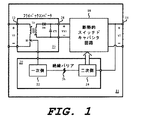
図1は、第1の段に接続する第1の端子12及び第2の段に接続する第2の端子14を有する二段電力変換回路11を示す。第1の端子12は、第1の電圧V1にあり、第2の端末14は、第2の電圧V2にある。
FIG. 1 shows a two-stage
例示される実施形態では、第1の段は、スイッチモードプリレギュレータ16として実施され、第2の段は、断熱的スイッチドキャパシタ回路18として実施される。しかしながら、代替実施形態では、この第2の段は、断熱的でない(non-adiabatic)、又は非断熱的(diabatic)である。
In the illustrated embodiment, the first stage is implemented as a
プリレギュレータ16は、その必須機能、すなわち出力電圧の調節が、実行可能である限り、いろいろな方法で実施されてもよい。例示される実施形態では、プリレギュレータ16は、プリレギュレータスイッチS0、トランスT0、ダイオードD0、及びフィルタキャパシタCXを含む。プリレギュレータ16の特に有用な実施は、磁気的に絶縁されたコンバータであり、その例は、フライバックコンバータである。
The pre-regulator 16 may be implemented in various ways as long as regulation of its essential function, ie output voltage, is feasible. In the illustrated embodiment, the pre-regulator 16 includes a pre-regulator switch S0, a transformer T0, a diode D0, and a filter capacitor CX. A particularly useful implementation of
いろいろなフライバックコンバータが、プリレギュレータ16を実施するために使用されてもよい。これらは、疑似共振フライバックコンバータ、アクティブクランプフライバックコンバータ、インターリーブフライバックコンバータ、及び2スイッチフライバックコンバータを含む。
Various flyback converters may be used to implement the
磁気的に絶縁されたコンバータの他の例は、フォワードコンバータである。適切なフォワードコンバータの例は、多重共振フォワードコンバータ、アクティブクランプフォワードコンバータ、インターリーブフォワードコンバータ、及び2スイッチフォワードコンバータを含む。 Another example of a magnetically isolated converter is a forward converter. Examples of suitable forward converters include multiple resonant forward converters, active clamp forward converters, interleaved forward converters, and two switch forward converters.
磁気的に絶縁されたコンバータのなお他の例は、ハーフブリッジコンバータ及びフルブリッジコンバータである。ハーフブリッジコンバータの例は、非対称ハーフブリッジコンバータ、多重共振ハーフブリッジコンバータ、及びLLC共振ハーフブリッジコンバータを含む。フルブリッジコンバータの例は、非対称フルブリッジコンバータ、多重共振フルブリッジコンバータ、及びLLC共振フルブリッジコンバータを含む。 Still other examples of magnetically isolated converters are half bridge converters and full bridge converters. Examples of half bridge converters include asymmetric half bridge converters, multi-resonant half bridge converters, and LLC resonant half bridge converters. Examples of full bridge converters include asymmetric full bridge converters, multi-resonant full bridge converters, and LLC resonant full bridge converters.
非絶縁のコンバータを使用してプリレギュレータ16を実施することもまた可能である。例は、バックコンバータ、ブーストコンバータ、及びバックブーストコンバータを含む。 It is also possible to implement the pre-regulator 16 using a non-isolated converter. Examples include buck converters, boost converters, and buck-boost converters.
本明細書で使用される場合、2つの機能コンポーネントは、もしエネルギーが、それらのコンポーネント間での直接的電気伝導経路なしにそれらのコンポーネント間で伝達可能であるならば、「絶縁されている」、又はより具体的には「DC的に絶縁されている」と言われる。したがって、そのような絶縁は、それらの間に流れる実際の電流を有することなく2つのコンポーネント間でエネルギーを伝達するための別の媒介の使用を前提とする。場合によっては、このエネルギーは、情報を含むこともある。 As used herein, two functional components are "isolated" if energy can be transferred between them without direct electrical conduction paths between the components. Or, more specifically, "DC isolated". Thus, such isolation presupposes the use of another intermediary to transfer energy between the two components without having an actual current flowing between them. In some cases, this energy may also contain information.
例は、電磁波、機械的な波、又は音響波などの、波の使用を含む。本明細書で使用される場合、電磁波は、可視領域、紫外領域、及び赤外領域の範囲にある波を含む。そのような絶縁はまた、準静的な電場又は磁場の使用を通じて、容量的に、誘導的に、又は機械的に媒介されてもよい。 Examples include the use of waves, such as electromagnetic waves, mechanical waves or acoustic waves. As used herein, electromagnetic waves include waves in the range of the visible, ultraviolet and infrared regions. Such insulation may also be capacitively, inductively or mechanically mediated through the use of quasi-static electric or magnetic fields.
大部分の機能コンポーネントは、回路の異なる部分が、異なる電位にある、回路を有する。しかしながら、その回路における最低電位を表す電位が常にある。これはしばしば、その回路についての「接地」と呼ばれる。 Most functional components have circuits in which different parts of the circuit are at different potentials. However, there is always a potential that represents the lowest potential in the circuit. This is often referred to as "ground" for the circuit.
第1及び第2の機能コンポーネントが、一緒に接続されるとき、第1のコンポーネントについての接地を規定する電位が、第2のコンポーネントについての接地を規定する電位と同じになるという保証はない。もしこれが、事実であり、これらのコンポーネントが、一緒に接続されるならば、電流が、2つの接地のより高い方から2つの接地のより低い方に流れることは、かなり可能性があることになる。「接地ループ」と呼ばれる、この条件は、望ましくない。もし2つのコンポーネントの1つが、たまたま人間であるならば、それは、特に望ましくない。そのような場合、接地ループ内の電流は、傷害を引き起こすこともある。 When the first and second functional components are connected together, there is no guarantee that the potential defining the ground for the first component will be the same as the potential defining the ground for the second component. If this is the case and these components are connected together, it is quite possible that current will flow from the higher of the two grounds to the lower of the two grounds. Become. This condition, called a "ground loop", is undesirable. It is particularly undesirable if one of the two components happens to be human. In such a case, the current in the ground loop may cause injury.
そのような接地ループは、2つのコンポーネントをDC的に絶縁することによって阻止できる。そのような絶縁は、本質的に接地ループの出現を排除し、電流が、人体などの、ある意図されない経路を通って接地に達することになるという可能性を低減する。 Such ground loops can be blocked by DC isolation of the two components. Such isolation essentially eliminates the appearance of ground loops and reduces the possibility that current will reach ground through some unintended path, such as the human body.
スイッチドキャパシタ回路18は、スイッチドキャパシタネットワークとして実施されてもよい。そのようなネットワークの例は、ラダーネットワーク、ディクソン(Dickson)ネットワーク、直並列ネットワーク、フィボナッチ(Fibonacci)ネットワーク、及びダブラー(Doubler)ネットワークを含む。これらはすべて、断熱的に充電され、多相ネットワークに構成されてもよい。特に有用なスイッチドキャパシタネットワークは、全波カスケード乗算器の断熱的に充電されるバージョンである。しかしながら、非断熱的に充電されるバージョンもまた、使用されてもよい。
The switched
本明細書で使用される場合、電荷をキャパシタ上に「断熱的に」変化することは、非容量性素子を通って電荷を通すことによって、そのキャパシタに蓄積されたある量の電荷を変化させることを意味する。キャパシタ上の電荷の正の断熱的変化は、断熱的充電と考えられ、一方キャパシタ上の電荷の負の断熱的変化は、断熱的放電と考えられる。非容量性素子の例は、インダクタ、磁気素子、抵抗器、及びそれらの組み合わせを含む。いずれにしても、結果は、キャパシタ上の電荷の量が、変化することができる比率に対する制約である。 As used herein, changing a charge "adiabatically" on a capacitor changes a certain amount of charge stored on that capacitor by passing the charge through a non-capacitive element It means that. Positive adiabatic change of charge on the capacitor is considered adiabatic charge, while negative adiabatic change of charge on the capacitor is considered adiabatic discharge. Examples of non-capacitive elements include inductors, magnetic elements, resistors, and combinations thereof. In any case, the result is a constraint on the rate at which the amount of charge on the capacitor can change.
場合によっては、キャパシタは、時間の一部について断熱的に充電され、時間の残りについて非断熱的に充電されてもよい。そのようなキャパシタは、断熱的に充電されると考えられる。同様に、場合によっては、キャパシタは、時間の一部について断熱的に放電され、時間の残りについて非断熱的に放電されてもよい。そのようなキャパシタは、断熱的に放電されると考えられる。 In some cases, the capacitor may be adiabatically charged for a portion of time and non-adiabatically charged for the remainder of time. Such capacitors are considered to be adiabatically charged. Similarly, in some cases, the capacitor may be adiabatically discharged for a portion of time and non-adiabatically discharged for the remainder of time. Such capacitors are considered to be adiabatically discharged.
非断熱的充電は、断熱的でないすべての充電を含み、非断熱的放電は、断熱的でないすべての放電を含む。 Non-adiabatic charging includes all non-adiabatic charging, and non-adiabatic discharging includes all non-adiabatic discharging.
本明細書で使用される場合、「断熱的スイッチドキャパシタ回路」は、断熱的に充電もされ、断熱的に放電もされる、少なくとも1つのキャパシタを有するネットワークである。「非断熱的スイッチドキャパシタ回路」は、断熱的スイッチドキャパシタ回路でないネットワークである。 As used herein, an "adiabatic switched capacitor circuit" is a network having at least one capacitor that is also adiabatically charged and adiabatically discharged. A "non-adiabatic switched capacitor circuit" is a network that is not an adiabatic switched capacitor circuit.
プリレギュレータ16、スイッチドキャパシタ回路18、それらの付随する回路、及びパッケージング技法の例は、米国特許第9,362,826号明細書、第9,497,854号明細書、第8,723,491号明細書、第8,503,203号明細書、第8,693,224号明細書、第9,502,968号明細書、第8,619,445号明細書、第9,203,299号明細書、及び第9,041,459号明細書、米国特許公開第2016/0197552号、第2015/0102798号、第2014/0301057号、2013/0154600号、第2015/0311786号、第2014/0327479号、第2016/0028302号、第2014/0266132号、第2015/0077175号、及び2015/0077176号、並びにPCT公開WO2014//062279、WO2015//138378、WO2015//138547、WO2016//149063、及びWO2017/007991に見いだすことができ、それらの内容は、参照により本明細書に組み込まれる。
Examples of
断熱的スイッチドキャパシタ回路は、2014年10月14日に発行された米国特許第8,860,396号明細書、2015年3月13日に両方とも出願された米国仮出願第62/132,701号及び第62/132,934号において詳細に述べられる。前述の文書の内容は、参照により本明細書に組み込まれる。 The adiabatic switched capacitor circuit is described in U.S. Pat. No. 8,860,396 issued Oct. 14, 2014 and U.S. Provisional Application No. 62/132, both filed Mar. 13, 2015. Nos. 701 and 62/132, 934 are described in detail. The contents of the aforementioned documents are incorporated herein by reference.
第1のコントローラ20は、第1及び第2の段の動作を制御する。第1のコントローラ20は、第1の段を制御する一次側22及び第2の段を制御する二次側24を含む。絶縁バリア26は、一次側22を二次側24から分離する。
The
第1のコントローラ20の一次側22は、プリレギュレータスイッチS0を制御する。プリレギュレータスイッチS0を開閉することは、トランスT0の一次側に提供される電流を制御する。これは次に、フィルタキャパシタCXにわたる電圧を制御する。プリレギュレータスイッチS0が、オンであるとき、ダイオードD0は、オフであり、プリレギュレータスイッチS0が、オフであるとき、ダイオードD0は、オンである。
The
プリレギュレータ16はまた、第1の電圧V1よりも低い中間電圧VX1に維持されるレギュレータ出力端子28も含む。このレギュレータ出力端子28は、断熱的スイッチドキャパシタ回路18に接続する。したがって、断熱的スイッチドキャパシタ回路18は、この中間電圧VX1を受け取り、それを第2の電圧V2に変圧する。
The pre-regulator 16 also includes a
断熱的スイッチドキャパシタ回路18は、個別のステップで動作する。したがって、それは、その出力の粗い調節を提供するだけである。それは、その出力の微細調節を提供することができない。それは、プリレギュレータ16がこの微細調節を実行するためである。図1に示される二段設計は、プリレギュレータ16が高電流負担を持続する必要性を低減する。これは、トランスT0の二次巻線が代わりに、はるかにより小さいRMS電流を運ぶことができるということを意味する。これは次に、巻線損失を低下させ、レギュレータ出力端子28における電圧リップルを低減する。それはまた、プリレギュレータ16を断熱的スイッチドキャパシタ回路18に結合するフィルタキャパシタCXが、より小さくできることも意味する。
The adiabatic switched
しかしながら、プリレギュレータ16の改善された性能は、断熱的スイッチドキャパシタ回路18を第2の段に有することによるサイズ及び電力損失の増加によって完全に相殺できない。したがって、断熱的スイッチドキャパシタ回路18が、極めて効率的でもあり、小さくもあるということは、不可欠である。
However, the improved performance of the pre-regulator 16 can not be completely offset by the increase in size and power loss due to having the adiabatic switched
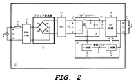
図1における二段電力変換回路11は、DC電圧を受け取るように構成されるとして示される。図2に示される代替実施形態では、結合キャパシタCBによって第1の端子12に結合されるブリッジ整流器65は、AC電圧VACを受け取る方法を提供する。
The two-stage
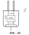
図2の電力変換回路10は、図1に示されるものに似ているが、しかしAC電源4によって提供されるAC電圧VACを受け取り、そのAC電圧VACを第2の電圧V2に変換するための追加の回路を有する。AC電圧VACは、ブリッジダイオードDB1、DB2、DB3、及びDB4がブリッジを形成するように配置され、ブリッジキャパシタCBにわたる出力を有するブリッジ整流器65の入力端子に提供される。ブリッジキャパシタCBにわたる出力は、第1の端子12に提示される第1の電圧V1になる。この種の電力変換回路10は、図22に示されるように、旅行用アダプタ13に組み込まれてもよい。そのような旅行用アダプタ13は、DC電圧をUSBポート15に出力する。
いくつかの実施形態は、高調波電流を制御し、したがって電力供給装置を通って流れる皮相電流(apparent power)に対する有効電力(real power)の比をブーストするための回路を含む。これは、AC電圧を供給する壁コンセントに結合する電力供給装置にとって特に有用である。そのような回路の例は、ブリッジ整流器65とプリレギュレータ16との間に配置されるアクティブ力率コレクタ67である。
Some embodiments include circuitry for controlling harmonic currents and thus boosting the ratio of real power to apparent power flowing through the power supply. This is particularly useful for power supplies that couple to a wall outlet that supplies AC voltage. An example of such a circuit is an active
図2はまた、AC電源4と電力変換回路10の残りのコンポーネントとの間の安全のためのヒューズ61も示す。電磁干渉フィルタ63もまた、電力変換回路10の動作中に生じることもある電磁波の制御されない放出を抑えるために提供される。
FIG. 2 also shows a
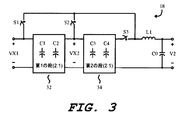
図3は、20ボルトの公称電圧を受け入れ、5ボルト及び10ボルトなどの、いろいろな出力電圧を生み出すように設計されるスイッチドキャパシタ回路18の第1の実施形態を示す。これは、C型旅行用アダプタにとって特に有用である。これは、出力が常に5ボルトである、より古いUSB標準と異なり、より新しいUSB C型標準が、10、15、さらには20ボルトなどの、より高い出力電圧を可能にするからである。
FIG. 3 shows a first embodiment of a switched
図3は、20ボルトの公称電圧を受け入れるように設計される断熱的スイッチドキャパシタ回路18の第1の実施形態を示す。例示される断熱的スイッチドキャパシタ回路18は、第1のスイッチドキャパシタ段32、第2のスイッチドキャパシタ段34、第1のバイパススイッチS1、第2のバイパススイッチS2、及び第3のバイパススイッチS3を特徴とする。出力インダクタL1及び出力キャパシタC0を有するLCフィルタは、断熱的動作を可能にする。バイパススイッチS1、S2、S3を選択的に開閉することによって、第1及び第2のスイッチドキャパシタ段32、34の選択される1つを選択的に迂回することが可能である。
FIG. 3 shows a first embodiment of an adiabatic switched
第1及び第2の段32、34の各々は、4:1のVX1からVX2への最大電圧変換を有する2X分圧器である。結果として得られる断熱的スイッチドキャパシタ回路18は、20ボルトの中間電圧VX1を受け入れ、20ボルト、10ボルト、又は5ボルトのいずれかの電圧を提供するように設計される。いくつかの実施形態は、時にはC型標準によって必要とされる、15ボルト出力電圧を配送する。これは、プリレギュレータ16に20ボルトの代わりに15ボルトをスイッチドキャパシタ回路18に配送させ、スイッチドキャパシタ回路18を1:1モードで動かすことによって提供可能である。
Each of the first and
図3に示される断熱的スイッチドキャパシタ回路18は、3つの動作モード、1:1モード、2:1モード、及び4:1モードを有する。1:1モードでは、第1のバイパススイッチS1は、閉じ、第2及び第3のバイパススイッチS2及びS3は、開く。2:1モードでは、第2のバイパススイッチS2は、閉じ、第1及び第3のバイパススイッチS1及びS3は、開く。4:1モードでは、第3のバイパススイッチS3は、閉じ、第1及び第2のバイパススイッチS1及びS2は、開く。すべての迂回される段は、それらが、電圧変換を提供するのに必要とされない(すなわち、それらが、特定の周波数でスイッチングしない)ので、電力を節約するために低電力モードで動く。
The adiabatic switched
図4は、第1の段32の内部のスイッチドキャパシタ回路36を例示する。同様の回路は、第2の段34内にある。動作中、この回路は、第1の状態と第2の状態との間で移行する。第1の状態では、「1」のラベル付きのすべてのスイッチは、閉じ、「2」のラベル付きのすべてのスイッチは、開く。第2の状態では、「1」のラベル付きのすべてのスイッチは、開き、「2」のラベル付きのすべてのスイッチは、閉じる。スイッチドキャパシタ回路36は、特定の周波数で第1の状態と第2の状態とを交互に繰り返す。この周波数は、中間電圧VX1の半分である第2の中間電圧VX2を生み出すために選択されるものである。
FIG. 4 illustrates the switched
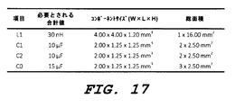
図5は、図3に示される断熱的スイッチドキャパシタ回路18の1つの実施のためのコンポーネントリストを示す。コンポーネントは、解決策が、高効率、小さい解決策サイズ、及び100mVピークツーピークの最大出力電圧リップルを提供するように選択された。合計値の列は、それらの動作条件におけるコンポーネントの必要とされるインダクタンス及び/又はキャパシタンスの総量を明示する。
FIG. 5 shows a component list for one implementation of the adiabatic switched
代替実施形態では、第1及び第2のバイパススイッチS1、S2は、第2の電圧V2が、制御された仕方でスルーアップ及びスルーダウンするといった方法でオン/オフされてもよい。これは、満たすべき最大スルーレートがあるときに特に有用である。例えば、第2の電圧V2が、5ボルトから20ボルトまでプログラム可能である、C型USB電力アダプタの場合、電圧移行について30mV/μsの最大スルーレート要件がある。 In an alternative embodiment, the first and second bypass switches S1, S2 may be turned on / off in such a way that the second voltage V2 slews up and down in a controlled manner. This is particularly useful when there is a maximum slew rate to meet. For example, for a C-type USB power adapter, where the second voltage V2 is programmable from 5 volts to 20 volts, there is a maximum slew rate requirement of 30 mV / μs for voltage migration.
図6は、第1及び第2のバイパススイッチ制御回路42が、図3に示される断熱的スイッチドキャパシタ回路18における電圧移行のスルーレートを制御するために追加される、図3の断熱的スイッチドキャパシタ回路18の代替実施形態を示す。これらのバイパススイッチ制御回路42は、出力が、5ボルトから10ボルトに及び5ボルトから20ボルトに移行するとき、図3に示される断熱的スイッチドキャパシタ回路18における電圧移行のスルーレートを制御する。バイパススイッチ制御回路42はまた、10ボルトから5ボルトへ及び20ボルトから5ボルトへの第2の電圧V2スルーレートも制御する。
FIG. 6 shows the adiabatic switch of FIG. 3 in which first and second bypass
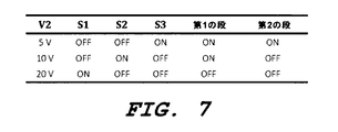
図7は、3つの異なる電圧出力についてのバイパススイッチ状態の表を示す。 FIG. 7 shows a table of bypass switch states for three different voltage outputs.
図6を参照すると、20ボルトを出力するために、人は、第1の制御入力V20をアサートする。10ボルトだけを出力するために、人は、第2の制御入力V10をアサートする。デフォルトにより、第1の出力も第2の出力も、アサートされないとき、断熱的スイッチドキャパシタ回路18は、5ボルトを出力する。
Referring to FIG. 6, in order to
図8は、図6に示されるバイパススイッチ制御回路42の詳細を示す。第2のバイパススイッチS2が、図8に示されるけれども、第1のバイパススイッチS1は、同様の方法で制御される。バイパススイッチS1、S2、及びS3のすべては、NチャンネルFET(NFET)である。第2及び第3のバイパススイッチS2及びS3のための複合バックトゥバック(back-to-back)NFET構成は、これらのスイッチが、オフであり、一方第1のバイパススイッチS1が、オンであるとき、出力から入力への逆電流の流れを遮断するために必要である。第2及び第3のバイパススイッチS2及びS3が、図8において個別のバックトゥバックNFETとして描写されるけれども、これらのデバイスは、完全に統合される解決策では適応可能な本体スイッチを有する単一トランジスタによって置き換えられてもよい。
FIG. 8 shows the details of the bypass
図8における第1のスルー制御スイッチS8は、第1及び第2のバイパススイッチS1、S2をそれらのゲート及びソース端子を短絡させることによってオフにする。第1のバイパススイッチS1か又は第2のバイパススイッチS2が、オンにされるとき、第1のスルー制御スイッチS8(それぞれの制御における)回路は、開き、第2の電圧V2は、5ボルトから10ボルトに又は5ボルトから20ボルトに移行する。その間に、抗スルーイング(anti-slewing)キャパシタC6及び定電流源I1は、5ボルトから10ボルトへ又は20ボルトへの第2の電圧V2移行の上向きスルーレートを制御する。 The first through control switch S8 in FIG. 8 turns off the first and second bypass switches S1, S2 by shorting their gate and source terminals. When the first bypass switch S1 or the second bypass switch S2 is turned on, the first through control switch S8 (in each control) circuit opens and the second voltage V2 is from 5 volts Transfer to 10 volts or from 5 volts to 20 volts. Meanwhile, an anti-slewing capacitor C6 and a constant current source I1 control the upward slew rate of the second voltage V2 transition from 5 volts to 10 volts or to 20 volts.
第1及び第2のバイパススイッチS1、S2が、オフにされ、第2の電圧V2が、10ボルトから5ボルトに又は20ボルトから5ボルトに移行するとき、第2のスルー制御スイッチS9は、オンになり、ブリーダ抵抗器R1が抗スルーイングキャパシタC6を放電することを可能にする。これは、第2の電圧V2の下向きスルーレートを制御する。 When the first and second bypass switches S1, S2 are turned off and the second voltage V2 transitions from 10 volts to 5 volts or from 20 volts to 5 volts, the second through control switch S9 is: It turns on and allows the bleeder resistor R1 to discharge the anti-slewing capacitor C6. This controls the downward slew rate of the second voltage V2.
図6における比較器は、第2の電圧V2があるしきい値VTH(例えば、VTH=5.25V)を下回って降下したときを検出し、第2のスルー制御スイッチS9を開くことによって抗スルーイングキャパシタC6の放電を終わらせる。ブリーダ抵抗器R1は、電流源によって置き換えられてもよく、正及び負の両方の電圧移行のスルーレートは、電流源I1、ブリーダ抵抗器R1、及び抗スルーイングキャパシタC6をプログラム可能又は再構成可能にすることによってプログラムされてもよいことに留意されたい。 The comparator in FIG. 6 detects when the second voltage V2 falls below a certain threshold value VTH (for example, VTH = 5.25 V), and prevents the through operation by opening the second through control switch S9. The discharge of the ing capacitor C6 is ended. The bleeder resistor R1 may be replaced by a current source, and the slew rate of both positive and negative voltage transitions can be programmed or reconfigured for the current source I1, the bleeder resistor R1 and the anti-slewing capacitor C6 Note that it may be programmed by
20ボルトが、出力に望まれるとき、第2及び第3のバイパススイッチS2、S3は、オフであり、一方第1のバイパススイッチS1は、オンである。第1及び第2の(2:1)スイッチドキャパシタ段もまた、オフである。第1のバイパススイッチS1は、NチャンネルFET(NFET)であり、そのターンオンは、第2の電圧V2が、定率でスルーアップするように、定電流源である電流源I1及び抗スルーイングキャパシタC6によって制御される。 When 20 volts is desired for output, the second and third bypass switches S2, S3 are off while the first bypass switch S1 is on. The first and second (2: 1) switched capacitor stages are also off. The first bypass switch S1 is an N-channel FET (NFET), whose turn on is constant current source I1 and anti-slewing capacitor C6 so that the second voltage V2 slews up at a constant rate. Controlled by
5ボルトから20ボルトへの移行中、第1及び第2のスルー制御スイッチS8、S9は、開いており、第1のバイパススイッチS1は、ソースフォロアーとしての役割を果たす。この構成では、第1のバイパススイッチS1のソース上の電圧は、そのゲート上の電圧に追随し、それは、抗スルーイングキャパシタC6のキャパシタンスで割られる、電流源I1を通る電流によって与えられる。最初に、第1のバイパススイッチS1が、オンになり、第2の電圧V2が、スルーアップするとき、第1のバイパススイッチS1は、飽和領域において動作する(すなわち、VDS>VGS−VT、ただしVTは、NFETのしきい電圧である)。出力が、その最終レベルに近づくにつれて、第1のバイパススイッチS1は、線形領域に移行し、低インピーダンススイッチとしての役割を果たす。ツェナーダイオードD1は、定常状態動作中はバイパススイッチS1のゲートソース間(gate-to-source)電圧(VGS1)を安全レベルにクランプする(例えば、VGS1は、5ボルトに等しい)。20ボルトから5ボルトに戻る移行は、ブリーダ抵抗器R1によって制御され、それは、スルーレートが制御される仕方で(in a slew-rate controlled manner)出力キャパシタンスを放電する。 During the transition from 5 volts to 20 volts, the first and second through control switches S8, S9 are open and the first bypass switch S1 acts as a source follower. In this configuration, the voltage on the source of the first bypass switch S1 follows the voltage on its gate, which is provided by the current through the current source I1 divided by the capacitance of the anti-slewing capacitor C6. First, when the first bypass switch S1 is turned on and the second voltage V2 passes through, the first bypass switch S1 operates in the saturation region (ie, V DS > V GS −V T 1 , where V T is the NFET threshold voltage). As the output approaches its final level, the first bypass switch S1 transitions into the linear region and acts as a low impedance switch. Zener diode D1 clamps the gate-to-source voltage (V GS1 ) of bypass switch S1 to a safe level during steady state operation (eg, V GS1 is equal to 5 volts). The transition from 20 volts back to 5 volts is controlled by bleeder resistor R1, which discharges the output capacitance in a slew-rate controlled manner.
10ボルトが、出力に望まれるとき、第1及び第3のバイパススイッチS1、S3は、オフであり、一方第2のバイパススイッチS2は、オンである。第1の(2:1)スイッチドキャパシタ段は、オンであり、第2のスイッチドキャパシタ段は、オフである。第2のバイパススイッチS2は、バックトゥバックNFETを含み、それは、第2の電圧V2が、5ボルトから10ボルトに移行するとき、ソースフォロアーとして動作する。前に述べられたように、電流源I1及び抗スルーイングキャパシタC6は、第2の電圧が、5ボルトから10ボルトに移行するとき、第2の電圧V2のスルーレートを制御し、ブリーダ抵抗器R1は、10ボルトから5ボルトに戻る移行を制御し、ツェナーダイオードD1は、10ボルト(すなわち、V2)での定常動作中は第2のバイパススイッチS2のゲートソース間電圧を安全レベルにクランプする。 When 10 volts is desired for the output, the first and third bypass switches S1, S3 are off, while the second bypass switch S2 is on. The first (2: 1) switched capacitor stage is on and the second switched capacitor stage is off. The second bypass switch S2 includes a back-to-back NFET, which acts as a source follower when the second voltage V2 transitions from 5 volts to 10 volts. As mentioned earlier, the current source I1 and the anti-slewing capacitor C6 control the slew rate of the second voltage V2 when the second voltage transitions from 5 volts to 10 volts, a bleeder resistor R1 controls the transition back from 10 volts to 5 volts, and the zener diode D1 clamps the gate-source voltage of the second bypass switch S2 to a safe level during steady operation at 10 volts (ie V2) .
図6及び図8に明確に示されないけれども、追加の回路が、あらゆるすべてのノード、スイッチ、及びパッシブコンポーネントへの過電流、過熱、及び過電圧などの、様々な単一点障害及び故障条件に対してシステムを保護するのに有用であることは、当業者によって理解されるはずである。 Although not explicitly shown in FIGS. 6 and 8, the additional circuitry is for various single point failure and failure conditions such as overcurrent, overheating, and overvoltage to any and all nodes, switches, and passive components. It should be understood by those skilled in the art that it is useful to protect the system.
図9は、C型USB電力アダプタにおけるスルーレートを制限されたバイパススイッチ制御を有するスイッチドキャパシタ回路についての典型的な電圧移行を示す。第2の電圧V2は、近似的に20mV/μsでスルーアップ及びスルーダウンする。USB PD仕様書によると、負荷は、電圧移行中は低電力待機状態になければならない。図9に示されるシミュレーション結果については、負荷は、出力が、その最終レベルに落ち着いた後、オンにされた。 FIG. 9 shows a typical voltage transition for a switched capacitor circuit with slew rate limited bypass switch control in a C-type USB power adapter. The second voltage V2 is slewed up and down at approximately 20 mV / μs. According to the USB PD specification, the load must be in a low power standby state during voltage transitions. For the simulation results shown in FIG. 9, the load was turned on after the output settled to its final level.
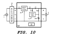
図10は、AC電源4に接続されるAC−DCコンバータ10から配送される電力を使用してバッテリBATを充電するためのエネルギーもまた提供しながら、負荷8に電力供給するためのエネルギーを提供する第1のバッテリマネージャ60Aを例示する。第1のバッテリマネージャ60Aは、負荷8に電力供給するためのシステム電圧VSYSを供給する。それは、AC−DCコンバータ10が、バッテリマネージャ60Aから切り離されるときでさえ、そうする。
FIG. 10 provides energy for powering the
AC電源4は、壁電源である必要はない。代わりに、AC電源4は、デバイスを充電するためのワイヤレス充電システムの一部とすることができる。そのようなワイヤレス充電システムは典型的には、基地局及び充電すべきデバイスを含む。基地局は、第1の周波数のACを受け取り、それをより高い周波数に上昇させ、それを周波数コンバータに提供し、周波数コンバータはそれを第1のコイルに提供する。充電すべきデバイスは、第1のコイルのすぐ近くに持ち込まれると、2つが、空芯トランスを形成するように選択される第2のコイルを含む。これは、第1のコイルによって提供されるエネルギーを第2のコイルにおいて利用可能にすることができ、その結果そのエネルギーは、充電すべきデバイス上のバッテリを充電するために使用できる。
The
より高い周波数への変換は、第1のコイルが妥当なサイズにできることを確実にするのに有用である。典型的な出力周波数は、50kHzの範囲にある。様々な標準は、基地局によって提供される電圧及び/又は電流の周波数遷移及び量の範囲について存在する。そのような標準の例は、QI標準である。 Conversion to a higher frequency is useful to ensure that the first coil can be of a reasonable size. Typical output frequencies are in the 50 kHz range. Various standards exist for the range of frequency transitions and amounts of voltage and / or current provided by the base station. An example of such a standard is the QI standard.
第1のバッテリマネージャ60Aは、AC−DCコンバータ10によって提供される第2の電圧V2をシステム電圧VSYSに変圧するステップダウンコンバータ56を含む。それはまた、バッテリBATを充電するための電力を提供する定電流/定電圧(CCCV)充電器52も含む。充電器52は、バッテリを充電しながら定電流又は定電圧のいずれかを維持するため、バッテリ上の電荷の量を測定するため、及び故障からの保護を提供するための回路を含む。ステップダウンコンバータ56は、バッテリによって電力供給されるデバイスの一部であるか、又はそれは、そのようなデバイスの外部に置かれてもよい。バッテリスイッチS4は、バッテリBATを選択的に負荷8に接続し、負荷8から切り離す。第2のコントローラ64は、ステップダウンコンバータ56及び充電器52の動作を同期させる。
The first battery manager 60A includes a step-
AC−DCコンバータ10が、AC電源4に接続するとき、バッテリBATは、電力を負荷8に提供するのに必要とされない。それに応じて、第2のコントローラ64は、バッテリスイッチS4を開く。その間に、ステップダウンコンバータ56は、第2の電圧V2をバッテリBATの充電電圧をわずかに上回る値まで低下させ、それによって、バッテリがすでに完全に充電されてはいないと仮定して、CC/CV充電器52がバッテリを効率的に充電することを可能にする。ステップダウンコンバータ56はまた、必要なシステム電圧VSYSを負荷8に提供もする。
When the AC-
しかしながら、いったんAC−DCコンバータ10が、切り離されると、ステップダウンコンバータ56は、もはや電力供給することができない。第2のコントローラ64は、したがって、バッテリBATが、必要なシステム電圧VSYSを提供することができるように、バッテリスイッチS4を閉じる。
However, once the AC-
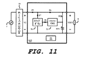
図11は、第2のバッテリマネージャ60Bを例示し、充電電圧及びシステム電圧VSYSは、第1のバッテリマネージャ60Aと異なり、分離される。バッテリスイッチS4は、バッテリが、システム電圧VSYSのための電力源として使用されるときに、閉じられるだけである。第1のバッテリマネージャ60Aを越えるこの第2のバッテリマネージャ60Bの利点は、AC−DCコンバータ10が、接続されるとき、ステップダウンコンバータ56が、バッテリBAT及びシステム電圧VSYSを充電するために電力供給する必要がないということである。
FIG. 11 illustrates a second battery manager 60B, wherein the charging voltage and the system voltage VSYS are separated unlike the first battery manager 60A. Battery switch S4 is only closed when the battery is used as a power source for system voltage VSYS. The advantage of this second battery manager 60B over the first battery manager 60A is that when the AC-
いくつかの実施形態では、AC−DCコンバータ10は、図2〜図4に例示される種類及びその変形の断熱的に充電されるスイッチドキャパシタコンバータを含む。
In some embodiments, AC-
図10及び図11は、図3に示される種類の断熱的スイッチドキャパシタ回路18が、第1及び第2のバッテリマネージャ60A、60B内に置かれてもよい、第1から第8の場所P1、P2・・・P8を集合的に示す。2つ以上の断熱的スイッチドキャパシタ回路18が、実際に使用されてもよいが、しかしながら、最大の性能改善は、単一の断熱的スイッチドキャパシタ回路18を組み込むことだけによって見られる可能性が高いことになる。
10 and 11 show adiabatic switched
図12は、断熱的スイッチドキャパシタ回路18が、第1の場所P1に置かれる、第3のバッテリマネージャ70Aを示す。断熱的スイッチドキャパシタ回路18を第3のバッテリマネージャ70Aに組み込むことは、ステップダウンコンバータ56への負担を低減する。例えば、図12に示される第3のバッテリマネージャ70Aでは、電圧ストレスは、断熱的スイッチドキャパシタ回路18が省略されていた場合のものの約半分である。これは、所与の出力電力についてステップダウンコンバータ56における電力損失を大幅に低減する効果を有する。
FIG. 12 shows a third battery manager 70A in which the adiabatic switched
図13は、断熱的スイッチドキャパシタ回路18が、代わりに第6の場所P6に置かれる、第4のバッテリマネージャ70Bを示す。断熱的スイッチドキャパシタ回路18の設置は、改善が、探し求められる、回路の部分を標的にするための方法を提供する。例えば、図13に示される第4のバッテリマネージャ70Bでは、主な改善は、ステップダウンコンバータ56にはなく、負荷8における下流の負荷端(POL,point−of−load)コンバータにある。
FIG. 13 shows a fourth battery manager 70B in which the adiabatic switched
図12及び図13に示される構成は、それらが、バッテリマネージャを実施する既存の集積回路と最も互換性があるので、特に有用である。 The configurations shown in FIGS. 12 and 13 are particularly useful as they are most compatible with existing integrated circuits implementing a battery manager.
図14は、断熱的スイッチドキャパシタ回路18が、第2の位置P2に置かれている、第5のバッテリマネージャ70Cを示す。図15は、断熱的スイッチドキャパシタ回路18が、第5の位置P5に置かれている、第6のバッテリマネージャ70Dを示す。
FIG. 14 shows a fifth battery manager 70C in which the adiabatic switched
図16は、典型的な断熱的スイッチドキャパシタ回路18のブロック図を示す。本回路は、入力電圧VX3から出力電圧V3への2:1電圧変換を提供する2X分圧器である。この断熱的スイッチドキャパシタ回路18は、24ボルトの最大入力電圧を受け入れるように設計される。
FIG. 16 shows a block diagram of a typical adiabatic switched
図17は、図16におけるアーキテクチャについての例となるコンポーネントリストを示す。 FIG. 17 shows an exemplary component list for the architecture in FIG.
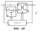
図10〜図11に示されるような典型的なステップダウンコンバータ56は、一般にスイッチングレギュレータを含む。それに応じて、いくつかの実施形態は、スイッチドキャパシタコンバータ86及び内蔵スイッチングレギュレータ88の両方を制御する第3のコントローラ84と一緒にスイッチドキャパシタコンバータ86をステップダウンコンバータ56に組み込む。したがって、第3のコントローラ84は、スイッチングレギュレータ88が、スイッチドキャパシタコンバータ86内のキャパシタを断熱的に充放電するような方法で、図18に示されるようにスイッチドキャパシタコンバータ86を動作させることができる。これは、スイッチドキャパシタコンバータ86とともに余分なLCフィルタを提供する必要なく断熱的な充電及び放電を達成する方法を提供する。加えて、この場合のスイッチドキャパシタコンバータ86は、本質的にモジュール式であり、既存のステップダウンコンバータ56に組み込むべき別個のコンポーネントとして容易に供給できる。
The exemplary step down
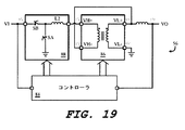
図19〜図20は、同じ概念を実施する2つの追加のアーキテクチャを例示する。図19に示される実施形態は、図18における実施形態の逆である。一方では、図20に示される実施形態は、スイッチドキャパシタコンバータ86の入力と直列に及びスイッチドキャパシタコンバータ86の出力と並列にスイッチングレギュレータ88を置くことによって電力を変換する効率的な方法を提供する。したがって、スイッチングレギュレータ88は、出力に配送される電流を直接制御する能力をなお保有しながら、出力に配送される電流のごく少量を運ぶだけである。
19-20 illustrate two additional architectures that implement the same concept. The embodiment shown in FIG. 19 is the reverse of the embodiment in FIG. On the one hand, the embodiment shown in FIG. 20 provides an efficient way of converting power by placing the switching
図18〜図20の実施形態における第3のコントローラ84は、感知される出力電圧VO及び/又は入力電圧VIに応答してスイッチングレギュレータ88及びスイッチドキャパシタコンバータ86内のスイッチをオン/オフさせるための制御信号を提供する。これらの入力に基づいて、コントローラ84は、出力電圧VOが、ある許容範囲内に調節されるように、スイッチングレギュレータ88及びスイッチドキャパシタコンバータ86に提供する制御信号に対して必要な調整をする。
The
例示される実施形態では、スイッチングレギュレータ88は、第1のスイッチSA、第2のスイッチSB、及びインダクタL2を含むバックコンバータである。第1のスイッチSAが、閉じられるとき、第2のスイッチSBは、開き、逆もまた同様である。第1及び第2のスイッチSA、SBは、特定の周波数で動作する。この周波数は、インダクタL2を通る平均DC電流を制御する。これは、第1のスイッチSAのデューティサイクルを変えることによってインダクタL2の出力端子(すなわち、スイッチに接続されない端子)における電圧を制御することを可能にする。特に、第1のスイッチSAが、サイクル中により長く閉じられているほど、インダクタL2の出力端子における電圧は、より低いことになる。
In the illustrated embodiment, the switching
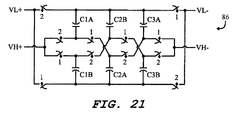
図21は、スイッチドキャパシタコンバータ86が、全波カスケード乗算器である、1つの実施の詳細な回路図を例示する。スイッチドキャパシタコンバータ86は、第1のスイッチセット1、第2のスイッチセット2、及びキャパシタC1A〜C3Bを含む。第1のスイッチセット1内のスイッチを閉じ、第2のスイッチセット2内のスイッチを開くことは、キャパシタC1A〜C3Bを第1の状態に配置する。反対に、第2のセット2内のスイッチを閉じ、第1のセット1内のスイッチを開くことは、キャパシタC1A〜C3Bを第2の状態に配置する。通常動作中、スイッチドキャパシタコンバータ86は、特定の周波数で第1の状態と第2の状態との間で循環し、それによって電荷をキャパシタC1A〜C3Bと端子との間で移動させる。スイッチドキャパシタコンバータ86は、図18〜図20におけるようなDCトランスとしてモデル化されてもよい。この実施では、電圧変換比(VH対VL)は、3対1である。
FIG. 21 illustrates a detailed schematic of one implementation where switched
いくつかの実施では、コンピュータアクセス可能記憶媒体は、コンバータの1又は2以上のコンポーネントを代表するデータベースを含む。例えば、データベースは、電荷ポンプの低損失動作を促進するように最適化されているスイッチングネットワークを代表するデータを含んでもよい。 In some implementations, a computer accessible storage medium includes a database representative of one or more components of the converter. For example, the database may include data representative of a switching network that has been optimized to facilitate low loss operation of the charge pump.
一般的に言えば、コンピュータアクセス可能記憶媒体は、命令及び/又はデータをコンピュータに提供するために使用する間、コンピュータによってアクセス可能である任意の非一時的記憶媒体を含んでもよい。例えば、コンピュータアクセス可能記憶媒体は、磁気ディスク又は光ディスク及び半導体メモリなどの記憶媒体を含んでもよい。 Generally speaking, a computer accessible storage medium may include any non-transitory storage medium accessible by a computer while used to provide instructions and / or data to the computer. For example, computer accessible storage media may include storage media such as magnetic disks or optical disks and semiconductor memory.
一般に、本システムを代表するデータベースは、プログラムによって読むことができ、本システムを備えるハードウェアを製作するために直接的に又は間接的に使用できるデータベース又は他のデータ構造であってもよい。例えば、データベースは、Verilog又はVHDLなどの高水準設計言語(HDL)におけるハードウェア機能性の動作レベル記述又はレジスタ転送レベル(RTL)記述であってもよい。本記述は、合成ライブラリからゲートのリストを備えるネットリストを作成するために本記述を合成することができる合成ツールによって読むことができる。ネットリストは、本システムを備えるハードウェアの機能性もまた表す一組のゲートを備える。ネットリストは次いで、マスクに適用すべき幾何学的形状を記述するデータセットを作成するために、設置され、ルートを決められてもよい。マスクは次いで、本システムに対応する半導体回路又は複数の半導体回路を作製するために様々な半導体製作ステップにおいて使用されてもよい。他の例では、別法として、データベースはそれ自体、ネットリスト(合成ライブラリを有する若しくは有さない)又はデータセットであってもよい。
In general, the database representative of the system may be a database or other data structure that can be read by a program and can be used directly or indirectly to make hardware comprising the system. For example, the database may be a behavioral level description or register transfer level (RTL) description of hardware functionality in a high level design language (HDL) such as Verilog or VHDL. The description can be read by a synthesis tool that can synthesize the description to create a netlist comprising a list of gates from a synthesis library. The netlist comprises a set of gates that also represent the functionality of the hardware comprising the system. The netlist may then be populated and routed to create a data set describing the geometry to be applied to the mask. The mask may then be used in various semiconductor fabrication steps to fabricate a semiconductor circuit or circuits corresponding to the present system. In another example, the database may itself be a netlist (with or without a synthetic library) or data set itself.
Claims (68)
Priority Applications (2)
| Application Number | Priority Date | Filing Date | Title |
|---|---|---|---|
| JP2021134510A JP2021184698A (en) | 2016-03-11 | 2021-08-20 | Battery management system having insulative switched capacitor circuit |
| JP2023149735A JP2023166566A (en) | 2016-03-11 | 2023-09-15 | Battery management system with adiabatic switched-capacitor circuit |
Applications Claiming Priority (3)
| Application Number | Priority Date | Filing Date | Title |
|---|---|---|---|
| US201662306749P | 2016-03-11 | 2016-03-11 | |
| US62/306,749 | 2016-03-11 | ||
| PCT/US2017/022104 WO2017156532A1 (en) | 2016-03-11 | 2017-03-13 | Battery management system with adiabatic switched-capacitor circuit |
Related Child Applications (1)
| Application Number | Title | Priority Date | Filing Date |
|---|---|---|---|
| JP2021134510A Division JP2021184698A (en) | 2016-03-11 | 2021-08-20 | Battery management system having insulative switched capacitor circuit |
Publications (2)
| Publication Number | Publication Date |
|---|---|
| JP2019512995A true JP2019512995A (en) | 2019-05-16 |
| JP2019512995A5 JP2019512995A5 (en) | 2020-04-23 |
Family
ID=59790874
Family Applications (3)
| Application Number | Title | Priority Date | Filing Date |
|---|---|---|---|
| JP2018546812A Pending JP2019512995A (en) | 2016-03-11 | 2017-03-13 | Battery management system with adiabatic switched capacitor circuit |
| JP2021134510A Pending JP2021184698A (en) | 2016-03-11 | 2021-08-20 | Battery management system having insulative switched capacitor circuit |
| JP2023149735A Pending JP2023166566A (en) | 2016-03-11 | 2023-09-15 | Battery management system with adiabatic switched-capacitor circuit |
Family Applications After (2)
| Application Number | Title | Priority Date | Filing Date |
|---|---|---|---|
| JP2021134510A Pending JP2021184698A (en) | 2016-03-11 | 2021-08-20 | Battery management system having insulative switched capacitor circuit |
| JP2023149735A Pending JP2023166566A (en) | 2016-03-11 | 2023-09-15 | Battery management system with adiabatic switched-capacitor circuit |
Country Status (5)
| Country | Link |
|---|---|
| US (2) | US20200295587A1 (en) |
| EP (2) | EP4135181A1 (en) |
| JP (3) | JP2019512995A (en) |
| CN (2) | CN109075703A (en) |
| WO (1) | WO2017156532A1 (en) |
Cited By (4)
| Publication number | Priority date | Publication date | Assignee | Title |
|---|---|---|---|---|
| JP2020190558A (en) * | 2019-05-23 | 2020-11-26 | フラバ ベスローテン ヴェンノーツハップFraba B.V. | Magnetic field sensor device |
| JP2021184698A (en) * | 2016-03-11 | 2021-12-02 | ピーセミ コーポレーションpSemi Corporation | Battery management system having insulative switched capacitor circuit |
| KR20220099335A (en) * | 2021-01-06 | 2022-07-13 | 주식회사 실리콘마이터스 | Power conversion circuit with battery cell balancing |
| WO2023054372A1 (en) * | 2021-09-29 | 2023-04-06 | 株式会社村田製作所 | Tracker module and communication device |
Families Citing this family (10)
| Publication number | Priority date | Publication date | Assignee | Title |
|---|---|---|---|---|
| WO2016149063A1 (en) | 2015-03-13 | 2016-09-22 | Arctic Sand Technologies, Inc. | Dc-dc transformer with inductor for the facilitation of adiabatic inter-capacitor charge transport |
| EP3804110A1 (en) * | 2018-05-24 | 2021-04-14 | Danmarks Tekniske Universitet | Reconfigurable ladder switched-capacitor converter |
| US11146172B2 (en) * | 2018-08-17 | 2021-10-12 | Texas Instruments Incorporated | Startup/brownout active clamping for capacitor-drop power supply |
| US10734893B1 (en) | 2019-05-03 | 2020-08-04 | Psemi Corporation | Driving circuit for switches used in a charge pump |
| KR20200136594A (en) * | 2019-05-28 | 2020-12-08 | 삼성전자주식회사 | Electronic device comprising voltage division circuitry adaptively changing voltage division ratio |
| US11223270B2 (en) | 2019-09-20 | 2022-01-11 | Cypress Semiconductor Corporation | Power-efficient sync-rectifier gate driver architecture |
| US10924006B1 (en) | 2019-09-30 | 2021-02-16 | Psemi Corporation | Suppression of rebalancing currents in a switched-capacitor network |
| CN113394859A (en) * | 2020-03-12 | 2021-09-14 | Oppo广东移动通信有限公司 | Power supply device and charging control method |
| CN113890354B (en) * | 2020-07-03 | 2024-04-09 | 华为技术有限公司 | Resonant switch capacitor circuit and electronic equipment |
| KR102607413B1 (en) * | 2021-08-12 | 2023-11-29 | 주식회사 효원파워텍 | Battery simulation apparatus having wide output range |
Citations (9)
| Publication number | Priority date | Publication date | Assignee | Title |
|---|---|---|---|---|
| JPH0787682A (en) * | 1993-09-20 | 1995-03-31 | Matsushita Electric Ind Co Ltd | Battery charger |
| JP2002233139A (en) * | 2001-02-05 | 2002-08-16 | Matsushita Electric Ind Co Ltd | Dc-dc converter |
| JP2004187355A (en) * | 2002-11-29 | 2004-07-02 | Fujitsu Ltd | Power supply control method, current/voltage conversion circuit, and electronic device |
| JP2007215320A (en) * | 2006-01-30 | 2007-08-23 | Samya Technology Co Ltd | Multifunction traveling charger |
| JP2009513098A (en) * | 2005-10-21 | 2009-03-26 | ザ リージェンツ オブ ザ ユニバーシティ オブ コロラド | System and method for receiving and managing power in a wireless device |
| US20090278520A1 (en) * | 2008-05-08 | 2009-11-12 | Perreault David J | Power Converter with Capacitive Energy Transfer and Fast Dynamic Response |
| JP2010521943A (en) * | 2007-08-01 | 2010-06-24 | インターシル アメリカズ インク | Capacitive voltage divider / buck converter / battery charger integrated voltage converter |
| US20150102798A1 (en) * | 2011-05-05 | 2015-04-16 | Arctic Sand Technologies, Inc. | Dc-dc converter with modular stages |
| JP2016504907A (en) * | 2013-10-28 | 2016-02-12 | アドバンスド チャージング テクノロジーズ, エルエルシーAdvanced Charging Technologies,Llc | Electric circuit for supplying power to home appliances |
Family Cites Families (25)
| Publication number | Priority date | Publication date | Assignee | Title |
|---|---|---|---|---|
| US5723970A (en) * | 1996-04-05 | 1998-03-03 | Linear Technology Corporation | Battery charging circuitry having supply current regulation |
| US6329796B1 (en) * | 2000-07-25 | 2001-12-11 | O2 Micro International Limited | Power management circuit for battery systems |
| US20090079385A1 (en) * | 2007-09-21 | 2009-03-26 | Msr Innovations Inc. | Solar powered battery charger using switch capacitor voltage converters |
| EP2218184A4 (en) * | 2007-11-19 | 2012-07-18 | Apple Inc | Charge recycling a 1 of n ndl gate with a time varying power supply |
| US9564772B2 (en) * | 2011-04-25 | 2017-02-07 | Intersil Americas LLC | Charging system with adaptive power management |
| US9882471B2 (en) | 2011-05-05 | 2018-01-30 | Peregrine Semiconductor Corporation | DC-DC converter with modular stages |
| US8743553B2 (en) | 2011-10-18 | 2014-06-03 | Arctic Sand Technologies, Inc. | Power converters with integrated capacitors |
| US8723491B2 (en) | 2011-12-19 | 2014-05-13 | Arctic Sand Technologies, Inc. | Control of power converters with capacitive energy transfer |
| US8704587B2 (en) * | 2012-07-23 | 2014-04-22 | Freescale Semiconductor, Inc. | Configurable multistage charge pump using a supply detect scheme |
| KR101432139B1 (en) * | 2012-09-05 | 2014-08-20 | 주식회사 실리콘웍스 | Switching Mode Converter Providing Safe Bootstrapping Enabling System On Chip And Method For Controlling Thereof |
| US8503203B1 (en) | 2012-10-16 | 2013-08-06 | Arctic Sand Technologies, Inc. | Pre-charge of switched capacitor circuits with cascoded drivers |
| US8693224B1 (en) | 2012-11-26 | 2014-04-08 | Arctic Sand Technologies Inc. | Pump capacitor configuration for switched capacitor circuits |
| US9847712B2 (en) | 2013-03-15 | 2017-12-19 | Peregrine Semiconductor Corporation | Fault control for switched capacitor power converter |
| US9203299B2 (en) | 2013-03-15 | 2015-12-01 | Artic Sand Technologies, Inc. | Controller-driven reconfiguration of switched-capacitor power converter |
| US8724353B1 (en) | 2013-03-15 | 2014-05-13 | Arctic Sand Technologies, Inc. | Efficient gate drivers for switched capacitor converters |
| US8619445B1 (en) | 2013-03-15 | 2013-12-31 | Arctic Sand Technologies, Inc. | Protection of switched capacitor power converter |
| JP6082969B2 (en) * | 2013-04-19 | 2017-02-22 | 国立研究開発法人宇宙航空研究開発機構 | Switched capacitor converter capable of PWM control |
| US9742266B2 (en) | 2013-09-16 | 2017-08-22 | Arctic Sand Technologies, Inc. | Charge pump timing control |
| US9041459B2 (en) | 2013-09-16 | 2015-05-26 | Arctic Sand Technologies, Inc. | Partial adiabatic conversion |
| KR102581009B1 (en) | 2014-03-14 | 2023-09-21 | 피세미 코포레이션 | Charge pump stability control |
| CN106105001B (en) | 2014-03-14 | 2019-07-09 | 北极砂技术有限公司 | The charge pump of charge balance controls |
| WO2015200437A1 (en) * | 2014-06-25 | 2015-12-30 | Emerson Network Power, Energy Systems, North America, Inc. | Battery backup units and systems including bypassing circuitry for regulating outputs |
| WO2016149063A1 (en) | 2015-03-13 | 2016-09-22 | Arctic Sand Technologies, Inc. | Dc-dc transformer with inductor for the facilitation of adiabatic inter-capacitor charge transport |
| KR20180019242A (en) | 2015-07-08 | 2018-02-23 | 페레그린 세미컨덕터 코포레이션 | Switched-capacitor power converters |
| CN109075703A (en) * | 2016-03-11 | 2018-12-21 | 派赛公司 | Battery management system with Adiabatic switching capacitor circuit |
-
2017
- 2017-03-13 CN CN201780028666.XA patent/CN109075703A/en active Pending
- 2017-03-13 JP JP2018546812A patent/JP2019512995A/en active Pending
- 2017-03-13 EP EP22157605.1A patent/EP4135181A1/en active Pending
- 2017-03-13 WO PCT/US2017/022104 patent/WO2017156532A1/en active Application Filing
- 2017-03-13 EP EP17764285.7A patent/EP3427375A4/en not_active Withdrawn
- 2017-03-13 US US16/084,041 patent/US20200295587A1/en not_active Abandoned
- 2017-03-13 CN CN202111508206.1A patent/CN114285113A/en active Pending
-
2021
- 2021-08-20 JP JP2021134510A patent/JP2021184698A/en active Pending
- 2021-12-03 US US17/457,497 patent/US20220166245A1/en active Pending
-
2023
- 2023-09-15 JP JP2023149735A patent/JP2023166566A/en active Pending
Patent Citations (9)
| Publication number | Priority date | Publication date | Assignee | Title |
|---|---|---|---|---|
| JPH0787682A (en) * | 1993-09-20 | 1995-03-31 | Matsushita Electric Ind Co Ltd | Battery charger |
| JP2002233139A (en) * | 2001-02-05 | 2002-08-16 | Matsushita Electric Ind Co Ltd | Dc-dc converter |
| JP2004187355A (en) * | 2002-11-29 | 2004-07-02 | Fujitsu Ltd | Power supply control method, current/voltage conversion circuit, and electronic device |
| JP2009513098A (en) * | 2005-10-21 | 2009-03-26 | ザ リージェンツ オブ ザ ユニバーシティ オブ コロラド | System and method for receiving and managing power in a wireless device |
| JP2007215320A (en) * | 2006-01-30 | 2007-08-23 | Samya Technology Co Ltd | Multifunction traveling charger |
| JP2010521943A (en) * | 2007-08-01 | 2010-06-24 | インターシル アメリカズ インク | Capacitive voltage divider / buck converter / battery charger integrated voltage converter |
| US20090278520A1 (en) * | 2008-05-08 | 2009-11-12 | Perreault David J | Power Converter with Capacitive Energy Transfer and Fast Dynamic Response |
| US20150102798A1 (en) * | 2011-05-05 | 2015-04-16 | Arctic Sand Technologies, Inc. | Dc-dc converter with modular stages |
| JP2016504907A (en) * | 2013-10-28 | 2016-02-12 | アドバンスド チャージング テクノロジーズ, エルエルシーAdvanced Charging Technologies,Llc | Electric circuit for supplying power to home appliances |
Cited By (5)
| Publication number | Priority date | Publication date | Assignee | Title |
|---|---|---|---|---|
| JP2021184698A (en) * | 2016-03-11 | 2021-12-02 | ピーセミ コーポレーションpSemi Corporation | Battery management system having insulative switched capacitor circuit |
| JP2020190558A (en) * | 2019-05-23 | 2020-11-26 | フラバ ベスローテン ヴェンノーツハップFraba B.V. | Magnetic field sensor device |
| KR20220099335A (en) * | 2021-01-06 | 2022-07-13 | 주식회사 실리콘마이터스 | Power conversion circuit with battery cell balancing |
| KR102528454B1 (en) | 2021-01-06 | 2023-05-04 | 주식회사 실리콘마이터스 | Power conversion circuit with battery cell balancing |
| WO2023054372A1 (en) * | 2021-09-29 | 2023-04-06 | 株式会社村田製作所 | Tracker module and communication device |
Also Published As
| Publication number | Publication date |
|---|---|
| WO2017156532A1 (en) | 2017-09-14 |
| CN109075703A (en) | 2018-12-21 |
| US20200295587A1 (en) | 2020-09-17 |
| EP4135181A1 (en) | 2023-02-15 |
| EP3427375A1 (en) | 2019-01-16 |
| CN114285113A (en) | 2022-04-05 |
| JP2021184698A (en) | 2021-12-02 |
| EP3427375A4 (en) | 2019-10-30 |
| US20220166245A1 (en) | 2022-05-26 |
| JP2023166566A (en) | 2023-11-21 |
Similar Documents
| Publication | Publication Date | Title |
|---|---|---|
| US20220166245A1 (en) | Battery management system with adiabatic switched-capacitor circuit | |
| US11411501B2 (en) | Slew-controlled switched capacitors for AC-DC applications | |
| US11646657B2 (en) | DC-DC transformer with inductor for the facilitation of adiabatic inter-capacitor charge transport | |
| US11764670B2 (en) | DC-DC converter with modular stages | |
| US20220337170A1 (en) | Switched capacitors for ac-dc applications | |
| US6911848B2 (en) | Low-loss transformer-coupled gate driver | |
| US8964438B2 (en) | Power converter with hold up | |
| Bertoni | RESONANT CLASS-E DC-DC CONVERTERS: an innovative analysis and design approach | |
| Chandrakasan et al. | DC Power Supply Design in Portable Systems | |
| NZ581311A (en) | A cyclo-converter with hold up capacity through an auxiliary converter with capacitors |
Legal Events
| Date | Code | Title | Description |
|---|---|---|---|
| A521 | Request for written amendment filed |
Free format text: JAPANESE INTERMEDIATE CODE: A523 Effective date: 20200313 |
|
| A621 | Written request for application examination |
Free format text: JAPANESE INTERMEDIATE CODE: A621 Effective date: 20200313 |
|
| A131 | Notification of reasons for refusal |
Free format text: JAPANESE INTERMEDIATE CODE: A131 Effective date: 20201019 |
|
| A977 | Report on retrieval |
Free format text: JAPANESE INTERMEDIATE CODE: A971007 Effective date: 20201021 |
|
| A521 | Request for written amendment filed |
Free format text: JAPANESE INTERMEDIATE CODE: A523 Effective date: 20210119 |
|
| A02 | Decision of refusal |
Free format text: JAPANESE INTERMEDIATE CODE: A02 Effective date: 20210420 |