JP2019175308A - Circuit device, electronic apparatus and cable harness - Google Patents

Circuit device, electronic apparatus and cable harness Download PDF

Info

Publication number
JP2019175308A
JP2019175308A JP2018065199A JP2018065199A JP2019175308A JP 2019175308 A JP2019175308 A JP 2019175308A JP 2018065199 A JP2018065199 A JP 2018065199A JP 2018065199 A JP2018065199 A JP 2018065199A JP 2019175308 A JP2019175308 A JP 2019175308A
Authority
JP
Japan
Prior art keywords
bus
circuit
physical layer
chirp
host
Prior art date
Legal status (The legal status is an assumption and is not a legal conclusion. Google has not performed a legal analysis and makes no representation as to the accuracy of the status listed.)
Pending
Application number
JP2018065199A
Other languages
Japanese (ja)
Inventor
利道 山田
Toshimichi Yamada
利道 山田
Current Assignee (The listed assignees may be inaccurate. Google has not performed a legal analysis and makes no representation or warranty as to the accuracy of the list.)
Seiko Epson Corp
Original Assignee
Seiko Epson Corp
Priority date (The priority date is an assumption and is not a legal conclusion. Google has not performed a legal analysis and makes no representation as to the accuracy of the date listed.)
Filing date
Publication date
Application filed by Seiko Epson Corp filed Critical Seiko Epson Corp
Priority to JP2018065199A priority Critical patent/JP2019175308A/en
Priority to CN201910235823.5A priority patent/CN110321311B/en
Priority to US16/367,485 priority patent/US10509756B2/en
Publication of JP2019175308A publication Critical patent/JP2019175308A/en
Pending legal-status Critical Current

Links

Images

Classifications

    • GPHYSICS
    • G06COMPUTING; CALCULATING OR COUNTING
    • G06FELECTRIC DIGITAL DATA PROCESSING
    • G06F13/00Interconnection of, or transfer of information or other signals between, memories, input/output devices or central processing units
    • G06F13/38Information transfer, e.g. on bus
    • G06F13/40Bus structure
    • G06F13/4063Device-to-bus coupling
    • GPHYSICS
    • G06COMPUTING; CALCULATING OR COUNTING
    • G06FELECTRIC DIGITAL DATA PROCESSING
    • G06F13/00Interconnection of, or transfer of information or other signals between, memories, input/output devices or central processing units
    • G06F13/38Information transfer, e.g. on bus
    • G06F13/40Bus structure
    • G06F13/4004Coupling between buses
    • G06F13/4022Coupling between buses using switching circuits, e.g. switching matrix, connection or expansion network
    • GPHYSICS
    • G06COMPUTING; CALCULATING OR COUNTING
    • G06FELECTRIC DIGITAL DATA PROCESSING
    • G06F13/00Interconnection of, or transfer of information or other signals between, memories, input/output devices or central processing units
    • G06F13/14Handling requests for interconnection or transfer
    • G06F13/20Handling requests for interconnection or transfer for access to input/output bus
    • GPHYSICS
    • G06COMPUTING; CALCULATING OR COUNTING
    • G06FELECTRIC DIGITAL DATA PROCESSING
    • G06F13/00Interconnection of, or transfer of information or other signals between, memories, input/output devices or central processing units
    • G06F13/38Information transfer, e.g. on bus
    • G06F13/42Bus transfer protocol, e.g. handshake; Synchronisation
    • G06F13/4282Bus transfer protocol, e.g. handshake; Synchronisation on a serial bus, e.g. I2C bus, SPI bus
    • BPERFORMING OPERATIONS; TRANSPORTING
    • B60VEHICLES IN GENERAL
    • B60RVEHICLES, VEHICLE FITTINGS, OR VEHICLE PARTS, NOT OTHERWISE PROVIDED FOR
    • B60R16/00Electric or fluid circuits specially adapted for vehicles and not otherwise provided for; Arrangement of elements of electric or fluid circuits specially adapted for vehicles and not otherwise provided for
    • B60R16/02Electric or fluid circuits specially adapted for vehicles and not otherwise provided for; Arrangement of elements of electric or fluid circuits specially adapted for vehicles and not otherwise provided for electric constitutive elements
    • B60R16/0207Wire harnesses
    • BPERFORMING OPERATIONS; TRANSPORTING
    • B60VEHICLES IN GENERAL
    • B60RVEHICLES, VEHICLE FITTINGS, OR VEHICLE PARTS, NOT OTHERWISE PROVIDED FOR
    • B60R16/00Electric or fluid circuits specially adapted for vehicles and not otherwise provided for; Arrangement of elements of electric or fluid circuits specially adapted for vehicles and not otherwise provided for
    • B60R16/02Electric or fluid circuits specially adapted for vehicles and not otherwise provided for; Arrangement of elements of electric or fluid circuits specially adapted for vehicles and not otherwise provided for electric constitutive elements
    • B60R16/023Electric or fluid circuits specially adapted for vehicles and not otherwise provided for; Arrangement of elements of electric or fluid circuits specially adapted for vehicles and not otherwise provided for electric constitutive elements for transmission of signals between vehicle parts or subsystems
    • GPHYSICS
    • G06COMPUTING; CALCULATING OR COUNTING
    • G06FELECTRIC DIGITAL DATA PROCESSING
    • G06F2213/00Indexing scheme relating to interconnection of, or transfer of information or other signals between, memories, input/output devices or central processing units
    • G06F2213/0042Universal serial bus [USB]
    • YGENERAL TAGGING OF NEW TECHNOLOGICAL DEVELOPMENTS; GENERAL TAGGING OF CROSS-SECTIONAL TECHNOLOGIES SPANNING OVER SEVERAL SECTIONS OF THE IPC; TECHNICAL SUBJECTS COVERED BY FORMER USPC CROSS-REFERENCE ART COLLECTIONS [XRACs] AND DIGESTS
    • Y02TECHNOLOGIES OR APPLICATIONS FOR MITIGATION OR ADAPTATION AGAINST CLIMATE CHANGE
    • Y02DCLIMATE CHANGE MITIGATION TECHNOLOGIES IN INFORMATION AND COMMUNICATION TECHNOLOGIES [ICT], I.E. INFORMATION AND COMMUNICATION TECHNOLOGIES AIMING AT THE REDUCTION OF THEIR OWN ENERGY USE
    • Y02D10/00Energy efficient computing, e.g. low power processors, power management or thermal management

Abstract

To provide a circuit device and the like capable of preventing occurrence of a trouble caused by on-resistance of a bus switch circuit while improving deterioration of a signal characteristic of a signal of USB.SOLUTION: A circuit device 10 comprises first and second physical layer circuits 11 and 12, a bus switch circuit 40 turning on connection between a first bus BS1 and a second bus BS2 of USB standard during a first period and turning off during a second period, and a processing circuit 20 performing packet transfer processing on a transfer path of the first bus BS1, the first and second physical layer circuits 11 and 12, and the second bus BS2 during the second period. When host chirp K/J is detected in the first bus BS1 by the first physical layer circuit 11, the second physical layer circuit 12 outputs the host chirp K/J to the second bus BS2 in a state in which the connection between the first bus BS1 and the second bus BS2 in the bus switch circuit 40 is turned off.SELECTED DRAWING: Figure 2

Description

本発明は、回路装置、電子機器及びケーブルハーネス等に関する。   The present invention relates to a circuit device, an electronic device, a cable harness, and the like.

従来より、USB(Universal Serial Bus)のデータ転送制御を実現する回路装置が知られている。このような回路装置の従来技術としては例えば特許文献1、2に開示される技術がある。例えば特許文献1には、HS(High Speed)モード用の送信回路の電流源のイネーブル制御信号を、パケットの送信開始タイミングの前のタイミングでアクティブにする技術が開示されている。特許文献2には、HSモードからFS(Full Speed)モードに切り替わった場合に、HSモード用の高速クロックを生成するPLLの自走動作をディスエーブルにする技術が開示されている。   2. Description of the Related Art Conventionally, circuit devices that realize USB (Universal Serial Bus) data transfer control are known. As a conventional technique of such a circuit device, there are techniques disclosed in Patent Documents 1 and 2, for example. For example, Patent Document 1 discloses a technique for activating an enable control signal for a current source of a transmission circuit for HS (High Speed) mode at a timing before the packet transmission start timing. Patent Document 2 discloses a technique for disabling the free-running operation of a PLL that generates a high-speed clock for the HS mode when the HS mode is switched to the FS (Full Speed) mode.

特開2006−135397号公報JP 2006-135397 A 特開2002−141911号公報JP 2002-141911 A

USBでは、HSモード用の送信回路が物理層回路に設けられる。しかしながら、HSモード用の送信回路の送信信号の信号経路には、寄生容量や寄生抵抗が存在するため、この寄生容量や寄生抵抗が原因となって、送信信号の信号特性が劣化してしまうという問題がある。このような問題を解決するために、USBのホストとデバイスの間に、信号特性を改善する回路装置を設ける手法が考えられる。しかしながら、この回路装置に設けられるバイパス用のスイッチ回路のオン抵抗が高いと、このオン抵抗が原因でUSBのチャープ信号の電圧が変動してしまうなどの問題が発生する。   In USB, a transmission circuit for the HS mode is provided in the physical layer circuit. However, since the parasitic signal and parasitic resistance exist in the signal path of the transmission signal of the transmission circuit for the HS mode, the signal characteristic of the transmission signal is deteriorated due to the parasitic capacitance and parasitic resistance. There's a problem. In order to solve such a problem, a method of providing a circuit device for improving signal characteristics between a USB host and a device can be considered. However, if the on-resistance of the bypass switch circuit provided in the circuit device is high, there arises a problem that the voltage of the USB chirp signal fluctuates due to the on-resistance.

本発明の一態様は、USB規格の第1バスが接続される第1物理層回路と、前記USB規格の第2バスが接続される第2物理層回路と、一端が前記第1バスに接続され、他端が前記第2バスに接続され、前記第1バスと前記第2バスとの間の接続を、第1期間においてオンにし、第2期間においてオフにするバススイッチ回路と、前記第1バスから前記第1物理層回路を介して受信したパケットを前記第2物理層回路を介して前記第2バスに送信し、前記第2バスから前記第2物理層回路を介して受信したパケットを前記第1物理層回路を介して前記第1バスに送信する転送処理を、前記第2期間において行う処理回路と、を含み、前記第2物理層回路は、前記第1物理層回路により前記第1バスにおいてホストチャープK/Jが検出されたときに、前記バススイッチ回路での前記第1バスと前記第2バスの接続がオフの状態で、前記第2バスに対してホストチャープK/Jを出力する回路装置に関係する。   One aspect of the present invention includes a first physical layer circuit to which a USB standard first bus is connected, a second physical layer circuit to which the USB standard second bus is connected, and one end connected to the first bus. The other end is connected to the second bus, the bus switch circuit that turns on the connection between the first bus and the second bus in the first period and turns off in the second period; Packets received from one bus via the first physical layer circuit are transmitted to the second bus via the second physical layer circuit, and packets received from the second bus via the second physical layer circuit A processing circuit for transmitting the first physical layer circuit to the first bus through the first physical layer circuit during the second period, and the second physical layer circuit is configured by the first physical layer circuit to Host chirp K / J detected on the first bus It comes to the connection of the first bus and said second bus in said bus switch circuit is off, related to the circuit device that outputs a host Chirp K / J with respect to the second bus.

また本発明の一態様では、前記第1物理層回路は、前記第2物理層回路により前記第2バスにおいてHSターミネーションが検出された場合に、前記第1物理層回路によるHSターミネーションをオンにしてもよい。   In the aspect of the invention, the first physical layer circuit may turn on HS termination by the first physical layer circuit when HS termination is detected in the second bus by the second physical layer circuit. Also good.

また本発明の一態様では、前記第1物理層回路は、前記第1物理層回路による前記HSターミネーションがオフの状態で、前記第1バスにおける前記ホストチャープK/Jを検出し、前記第2物理層回路により前記第2バスにおいて前記HSターミネーションが検出された場合に、前記第1物理層回路による前記HSターミネーションをオンにしてもよい。   In the aspect of the invention, the first physical layer circuit may detect the host chirp K / J in the first bus in a state where the HS termination by the first physical layer circuit is off, and When the HS termination is detected in the second bus by the physical layer circuit, the HS termination by the first physical layer circuit may be turned on.

また本発明の一態様では、前記第1物理層回路は、前記第2バスにおいてデバイスチャープKが検出されたときに、前記バススイッチ回路での前記第1バスと前記第2バスの接続がオフの状態で、前記第1バスに対してデバイスチャープKを出力してもよい。   In the aspect of the invention, the first physical layer circuit may turn off the connection between the first bus and the second bus in the bus switch circuit when the device chirp K is detected in the second bus. In this state, the device chirp K may be output to the first bus.

また本発明の一態様では、前記バススイッチ回路での電流検出を行う検出回路を含み、前記第1物理層回路は、USBのバスリセット後に前記第2バスから前記バススイッチ回路を介して前記第1バスに電流が流れたことが、前記検出回路により検出されたときに、前記第1バスに対して前記デバイスチャープKを出力してもよい。   According to another aspect of the present invention, the first physical layer circuit includes a detection circuit configured to detect a current in the bus switch circuit, and the first physical layer circuit is connected to the second bus from the second bus via the bus switch circuit after a USB bus reset. The device chirp K may be output to the first bus when the detection circuit detects that a current has flowed through one bus.

また本発明の一態様では、前記第2バスから前記バススイッチ回路を介して前記第1バスに電流が流れたことが、前記検出回路により検出されたときに、前記バススイッチ回路は、前記第1バスと前記第2バスの接続をオンからオフにし、前記第2物理層回路は、前記第2物理層回路によるHSターミネーションをオンにしてもよい。   In the aspect of the invention, when the detection circuit detects that a current has flowed from the second bus to the first bus via the bus switch circuit, the bus switch circuit The connection between one bus and the second bus may be turned off from on, and the second physical layer circuit may turn on HS termination by the second physical layer circuit.

また本発明の一態様では、前記検出回路は、前記バスリセット後に前記第2バスから前記バススイッチ回路を介して前記第1バスに電流が流れたときに、前記第1バスがアップストリーム側のバスであり、前記第2バスがダウンストリーム側のバスであると検出し、前記バスリセット後に前記第1バスから前記バススイッチ回路を介して前記第2バスに電流が流れたときに、前記第1バスがダウンストリーム側のバスであり、前記第2バスがアップストリーム側のバスであると検出してもよい。   In the aspect of the invention, the detection circuit may be configured such that when a current flows from the second bus to the first bus through the bus switch circuit after the bus reset, the first bus is on the upstream side. The second bus is detected as a downstream bus, and the current flows from the first bus to the second bus through the bus switch circuit after the bus reset. It may be detected that one bus is a downstream bus and the second bus is an upstream bus.

また本発明の一態様では、前記第1物理層回路は、前記第2バスにおいて前記デバイスチャープKの出力の停止が検出されたときに、前記第1バスに対する前記デイバスチャープKの出力を停止してもよい。   In one aspect of the present invention, the first physical layer circuit stops the output of the device chirp K to the first bus when the stop of the output of the device chirp K is detected in the second bus. May be.

また本発明の一態様では、前記第2物理層回路は、前記第2バスでの前記デバイスチャープKの停止の後に、前記第1物理層回路により前記第1バスにおいて前記ホストチャープK/Jが検出されたときに、前記第2バスに対して前記ホストチャープK/Jを出力してもよい。   Also, in one aspect of the present invention, the second physical layer circuit causes the host chirp K / J to be set in the first bus by the first physical layer circuit after the device chirp K is stopped in the second bus. When detected, the host chirp K / J may be output to the second bus.

また本発明の一態様は、USB規格の第1バスが接続される第1物理層回路と、前記USB規格の第2バスが接続される第2物理層回路と、一端が前記第1バスに接続され、他端が前記第2バスに接続され、前記第1バスと前記第2バスとの間の接続を、第1期間においてオンにし、第2期間においてオフにするバススイッチ回路と、前記第1バスから前記第1物理層回路を介して受信したパケットを前記第2物理層回路を介して前記第2バスに送信し、前記第2バスから前記第2物理層回路を介して受信したパケットを前記第1物理層回路を介して前記第1バスに送信する転送処理を、前記第2期間において行う処理回路と、USBのバスリセット後に前記第2バスから前記バススイッチ回路を介して前記第1バスに電流が流れたときに、前記第1バスがアップストリーム側のバスであり、前記第2バスがダウンストリーム側のバスであると検出し、前記バスリセット後に前記第1バスから前記バススイッチ回路を介して前記第2バスに電流が流れたときに、前記第1バスがダウンストリーム側のバスであり、前記第2バスがアップストリーム側のバスであると検出する検出回路と、を含む回路装置に関係する。   One embodiment of the present invention includes a first physical layer circuit to which a USB standard first bus is connected, a second physical layer circuit to which the USB standard second bus is connected, and one end connected to the first bus. A bus switch circuit that is connected, the other end is connected to the second bus, and the connection between the first bus and the second bus is turned on in a first period and turned off in a second period; A packet received from the first bus via the first physical layer circuit is transmitted to the second bus via the second physical layer circuit and received from the second bus via the second physical layer circuit. A transfer circuit for transmitting a packet to the first bus via the first physical layer circuit, a processing circuit for performing the second period, and a USB bus reset after the bus reset from the second bus via the bus switch circuit. When current flows through the first bus, The first bus is detected as an upstream bus, and the second bus is detected as a downstream bus. After the bus reset, the first bus is transferred to the second bus via the bus switch circuit. And a detection circuit that detects that the first bus is a downstream bus and the second bus is an upstream bus when a current flows.

また本発明の一態様では、L前記第1物理層回路は、前記バスリセット後に前記第2バスから前記バススイッチ回路を介して前記第1バスに電流が流れたことが、前記検出回路により検出されたときに、前記第1バスに対してデバイスチャープKを出力してもよい。   In one aspect of the present invention, the first physical layer circuit detects that the current has flowed from the second bus to the first bus through the bus switch circuit after the bus reset. When this is done, a device chirp K may be output to the first bus.

また本発明の一態様では、前記第2物理層回路は、前記第1物理層回路により前記第1バスにおいてホストチャープK/Jが検出されたときに、前前記第2バスに対してホストチャープK/Jを出力してもよい。   In one aspect of the present invention, the second physical layer circuit may be configured such that when the first physical layer circuit detects a host chirp K / J on the first bus, the second physical layer circuit K / J may be output.

また本発明の他の態様は、上記に記載の前記回路装置と、前記第1バスに接続される処理装置と、を含む電子機器に関係する。   Another aspect of the invention relates to an electronic apparatus including the circuit device described above and a processing device connected to the first bus.

また本発明の他の態様は、上記に記載の前記回路装置と、ケーブルと、を含むケーブルハーネスに関係する。   Another aspect of the present invention relates to a cable harness including the circuit device described above and a cable.

送信信号の信号特性の劣化の問題についての説明図。Explanatory drawing about the problem of the deterioration of the signal characteristic of a transmission signal. 本実施形態の回路装置の構成例。1 is a configuration example of a circuit device according to the present embodiment. 回路装置の詳細な構成例。3 shows a detailed configuration example of a circuit device. 回路装置の具体的な構成例。The specific structural example of a circuit apparatus. 回路装置の動作説明図。FIG. 6 is an operation explanatory diagram of the circuit device. 回路装置の動作説明図。FIG. 6 is an operation explanatory diagram of the circuit device. 物理層回路の構成例。The structural example of a physical layer circuit. HSドライバーの構成例。Configuration example of HS driver. オン抵抗を原因とする信号特性の劣化についての説明図。Explanatory drawing about deterioration of the signal characteristic resulting from on-resistance. USBのFSからHSへの移行シーケンスを説明する信号波形図。The signal waveform diagram explaining the transfer sequence from FS of USB to HS. デバイスチャープKの説明図。Explanatory drawing of device chirp K. FIG. ホストチャープK/Jの説明図。Explanatory drawing of host chirp K / J. ホストチャープK/Jの説明図。Explanatory drawing of host chirp K / J. 回路装置の詳細な動作を説明する信号波形図。The signal waveform diagram explaining the detailed operation | movement of a circuit apparatus. FSからHSへの移行シーケンスでの本実施形態の詳細な動作説明図。The detailed operation explanatory view of this embodiment in the transition sequence from FS to HS. FSからHSへの移行シーケンスでの本実施形態の詳細な動作説明図。The detailed operation explanatory view of this embodiment in the transition sequence from FS to HS. FSからHSへの移行シーケンスでの本実施形態の詳細な動作説明図。The detailed operation explanatory view of this embodiment in the transition sequence from FS to HS. FSからHSへの移行シーケンスでの本実施形態の詳細な動作説明図。The detailed operation explanatory view of this embodiment in the transition sequence from FS to HS. FSからHSへの移行シーケンスでの本実施形態の詳細な動作説明図。The detailed operation explanatory view of this embodiment in the transition sequence from FS to HS. FSからHSへの移行シーケンスでの本実施形態の詳細な動作説明図。The detailed operation explanatory view of this embodiment in the transition sequence from FS to HS. HSのリセット時の本実施形態の動作シーケンを説明する信号波形図。The signal waveform diagram explaining the operation | movement sequence of this embodiment at the time of HS reset. HSのサスペンド時の本実施形態の動作シーケンを説明する信号波形図。The signal waveform diagram explaining the operation | movement sequence of this embodiment at the time of suspension of HS. 電子機器の構成例。Configuration example of an electronic device. ケーブルハーネスの構成例。Configuration example of cable harness.

以下、本発明の好適な実施の形態について詳細に説明する。なお以下に説明する本実施形態は特許請求の範囲に記載された本発明の内容を不当に限定するものではなく、本実施形態で説明される構成の全てが本発明の解決手段として必須であるとは限らない。   Hereinafter, preferred embodiments of the present invention will be described in detail. The present embodiment described below does not unduly limit the contents of the present invention described in the claims, and all the configurations described in the present embodiment are indispensable as means for solving the present invention. Not necessarily.

1.送信信号の信号特性
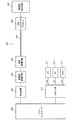
図1を用いてUSBでの送信信号の信号特性の劣化を説明する。図1は車載の電子機器のシステムの一例を示すものであり、ホストであるメインコントローラー200にはUSB−HUB210が接続される。例えばUSB−HUB210のアップストリームポートがメインコントローラー200に接続され、ダウンストリームポートには、SD211、BT212、DSRC213(Dedicated Short Range Communications)などのデバイスが接続される。SD211はSDカードの機器であり、BT212はブルートゥース(登録商標)の機器である。またケーブル224を有するケーブルハーネス220のUSBレセプタクル226には、スマートフォンなどの携帯型端末装置250が接続される。メインコントローラー200とUSBレセプタクル226の間には、充電回路221、静電気保護回路222、短絡保護回路223などが設けられている。
1. Signal Characteristics of Transmission Signal Deterioration of signal characteristics of a transmission signal in USB will be described with reference to FIG. FIG. 1 shows an example of a system of an in-vehicle electronic device, and a USB-HUB 210 is connected to a main controller 200 that is a host. For example, the upstream port of the USB-HUB 210 is connected to the main controller 200, and devices such as SD211, BT212, DSRC213 (Dedicated Short Range Communications) are connected to the downstream port. SD211 is an SD card device, and BT212 is a Bluetooth (registered trademark) device. A portable terminal device 250 such as a smartphone is connected to the USB receptacle 226 of the cable harness 220 having the cable 224. Between the main controller 200 and the USB receptacle 226, a charging circuit 221, an electrostatic protection circuit 222, a short circuit protection circuit 223, and the like are provided.

図1では、ケーブル224は車内において例えば内装を避けて配線されるため、ケーブル長が非常に長くなり、寄生容量等が生じる。また充電回路221、静電気保護回路222、短絡保護回路223などの回路に起因する寄生容量等も生じる。これらの寄生容量等が原因となって、メインコントローラー200が有するUSBのHSの送信信号の信号特性が劣化する。一方、USBの認証テストにおいては送信信号の波形がアイパターンの禁止領域と重ならないようにすることが要求される。ところが図1において車内で引き回されるケーブル224が長くなることなどにより、送信信号の信号品質が悪化すると、適正な信号転送を実現できなくなり、アイパターンのニアエンドの認証テストなどをパスできないなどの問題が生じる。   In FIG. 1, since the cable 224 is wired in the vehicle while avoiding the interior, for example, the cable length becomes very long, and parasitic capacitance or the like occurs. In addition, parasitic capacitance and the like due to circuits such as the charging circuit 221, the electrostatic protection circuit 222, and the short circuit protection circuit 223 also occur. Due to these parasitic capacitances and the like, the signal characteristics of the USB HS transmission signal of the main controller 200 deteriorate. On the other hand, in the USB authentication test, it is required that the waveform of the transmission signal does not overlap with the prohibited area of the eye pattern. However, if the signal quality of the transmission signal deteriorates due to the length of the cable 224 routed in the vehicle in FIG. 1, proper signal transfer cannot be realized, and the eye pattern near-end authentication test cannot be passed. Problems arise.

2.回路装置の構成例
図2に本実施形態の回路装置10の構成例を示す。回路装置10は、第1物理層回路11と、第2物理層回路12と、処理回路20と、バススイッチ回路40を含む。なお回路装置10は図2の構成には限定されず、これらの一部の構成要素を省略したり、他の構成要素を追加するなどの種々の変形実施が可能である。
2. Configuration Example of Circuit Device FIG. 2 shows a configuration example of the circuit device 10 of the present embodiment. The circuit device 10 includes a first physical layer circuit 11, a second physical layer circuit 12, a processing circuit 20, and a bus switch circuit 40. The circuit device 10 is not limited to the configuration in FIG. 2, and various modifications such as omitting some of these components or adding other components are possible.

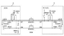
第1物理層回路11にはUSB規格の第1バスBS1が接続される。第2物理層回路12にはUSB規格の第2バスBS2が接続される。第1、第2物理層回路11、12の各々は、物理層のアナログ回路により構成される。物理層のアナログ回路は、例えばHS、FS用の送信回路であるドライバー、HS、FS用の受信回路であるレシーバー、各種の検出回路、プルアップ抵抗回路などである。なお、USBを介して受信したシリアルデータをパラレルデータに変換するシリアル/パラレル変換回路や、パラレルデータをシリアルデータに変換するパラレル/シリアル変換回路や、エラスティックバッファーや、NRZI回路などのリンク層に相当する回路は、処理回路20に含まれる。USBのトランシーバマクロセルのうちのリンク層等に相当する回路は処理回路20に含まれ、送信回路、受信回路、検出回路等のアナログ回路が第1、第2物理層回路11、12に含まれる。   The first physical layer circuit 11 is connected to a USB standard first bus BS1. A USB standard second bus BS2 is connected to the second physical layer circuit 12. Each of the first and second physical layer circuits 11 and 12 is configured by an analog circuit in the physical layer. The analog circuit in the physical layer includes, for example, a driver that is a transmission circuit for HS and FS, a receiver that is a reception circuit for HS and FS, various detection circuits, and a pull-up resistor circuit. Note that serial / parallel conversion circuits that convert serial data received via USB into parallel data, parallel / serial conversion circuits that convert parallel data into serial data, elastic buffers, NRZI circuits, and other link layers A corresponding circuit is included in the processing circuit 20. A circuit corresponding to a link layer or the like in the USB transceiver macrocell is included in the processing circuit 20, and analog circuits such as a transmission circuit, a reception circuit, and a detection circuit are included in the first and second physical layer circuits 11 and 12.

第1バスBS1は例えばホスト側が接続されるバスであり、第2バスBS2は例えばデバイス側が接続されるバスである。但し本実施形態はこのような接続構成に限定されるものではない。第1バスBS1、第2バスBS2は、差動信号を構成する第1、第2信号である信号DP(DataPlus)、信号DM(DataMinus)の信号線を含むUSB規格のバスである。第1バスBS1、第2バスBS2は電源VBUS、GNDの信号線を含むことができる。USB規格は広義には所与のデータ転送の規格である。   For example, the first bus BS1 is a bus to which the host side is connected, and the second bus BS2 is a bus to which the device side is connected, for example. However, the present embodiment is not limited to such a connection configuration. The first bus BS1 and the second bus BS2 are USB standard buses including signal lines of a signal DP (DataPlus) and a signal DM (DataMinus) which are first and second signals constituting a differential signal. The first bus BS1 and the second bus BS2 may include signal lines for power supplies VBUS and GND. The USB standard is a standard for given data transfer in a broad sense.

バススイッチ回路40は、一端が第1バスBS1に接続され、他端が第2バスBS2に接続される。そして第1バスBS1と第2バスBS2との間の接続をオン又はオフにする。即ち、第1バスBS1と第2バスBS2を電気的に接続したり、電気的に非接続にする。第1バスBS1と第2バスBS2との間の接続をオン又はオフにするとは、例えば第1バスBS1のDP、DMの信号線と第2バスBS2のDP、DMの信号線の間に設けられるスイッチ素子などをオン又はオフにすることである。また本実施形態における回路間の接続やバス又は信号線と回路との接続は、電気的な接続である。電気的な接続とは、電気信号が伝達可能に接続されていることであり、電気信号による情報の伝達が可能となる接続である。電気的な接続は例えば信号線や能動素子等を介した接続であってもよい。   The bus switch circuit 40 has one end connected to the first bus BS1 and the other end connected to the second bus BS2. Then, the connection between the first bus BS1 and the second bus BS2 is turned on or off. That is, the first bus BS1 and the second bus BS2 are electrically connected or not electrically connected. To turn on or off the connection between the first bus BS1 and the second bus BS2, for example, it is provided between the DP and DM signal lines of the first bus BS1 and the DP and DM signal lines of the second bus BS2. The switching element or the like to be turned on or off. Further, the connection between circuits and the connection between the bus or signal line and the circuit in this embodiment are electrical connections. The electrical connection means that an electrical signal is transmitted so that information can be transmitted by the electrical signal. The electrical connection may be, for example, a connection via a signal line or an active element.

具体的には後述の図5に示すように、バススイッチ回路40は、第1バスBS1と第2バスBS2との間の接続を、第1期間T1においてオンにする。即ち、バススイッチ回路40は、第1バスBS1と第2バスBS2との間に設けられるスイッチ素子を有し、第1期間T1において、当該スイッチ素子がオンになる。これにより、第1バスBS1に接続されるメインコントローラー200と第2バスBS2に接続されるペリフェラルデバイス260とが、USBのバスにより直接にUSBの信号転送を行うことが可能になる。なおスイッチ素子としては例えば信号DP用のスイッチ素子と信号DM用のスイッチ素子が設けられる。またメインコントローラー200、ペリフェラルデバイス260は広義には第1装置、第2装置である。また後述の図6に示すように、バススイッチ回路40は、第1バスBS1と第2バスBS2との間の接続を、第2期間T2においてオフにする。即ち、第2期間T2において、第1バスBS1と第2バスBS2との間に設けられるスイッチ素子がオフになる。処理回路20は、この第2期間T2において、下述する転送処理を行うことになる。   Specifically, as shown in FIG. 5 described later, the bus switch circuit 40 turns on the connection between the first bus BS1 and the second bus BS2 in the first period T1. That is, the bus switch circuit 40 includes a switch element provided between the first bus BS1 and the second bus BS2, and the switch element is turned on in the first period T1. As a result, the main controller 200 connected to the first bus BS1 and the peripheral device 260 connected to the second bus BS2 can directly transfer USB signals through the USB bus. As the switch elements, for example, a switch element for signal DP and a switch element for signal DM are provided. The main controller 200 and the peripheral device 260 are a first device and a second device in a broad sense. As shown in FIG. 6 described later, the bus switch circuit 40 turns off the connection between the first bus BS1 and the second bus BS2 in the second period T2. That is, in the second period T2, the switch element provided between the first bus BS1 and the second bus BS2 is turned off. The processing circuit 20 performs the transfer process described below in the second period T2.

処理回路20は、転送処理や各種の制御処理を行う回路であり、ゲートアレイなどの自動配置配線によるロジック回路などにより実現できる。なお処理回路20をCPU、MPU等のプロセッサーにより実現してもよい。そして処理回路20は、第1バスBS1から第1物理層回路11を介して受信したパケットを第2物理層回路12を介して第2バスBS2に送信し、第2バスBS2から第2物理層回路12を介して受信したパケットを第1物理層回路11を介して第1バスBS1に送信する転送処理を、第2期間T2において行う。例えば少なくとも第2期間T2の一部において当該転送処理を行う。例えば第1バスBS1側から第2バスBS2側に、或いは第2バスBS2側から第1バスBS1側に、パケットフォーマットを変更することなくパケットを転送する。このとき処理回路20は、当該転送処理において、所定の信号処理を行う。所定の信号処理は、パケット転送のための信号処理であり、受信したパケットのリピートパケットを転送するための信号処理である。例えば処理回路20は、所定の信号処理として、所定パケットのビットの再同期化処理を行う。例えばパケットの受信の際には、回路装置10で生成されたクロック信号に基づいてパケットの各ビットをサンプリングする。パケットの送信の際には、回路装置10で生成されたクロック信号に同期してパケットの各ビットを送信する。処理回路20を経由した図6の転送経路TR2でパケット転送を行う際に、処理回路20が所定の信号処理を行うことで、USBの送信信号の信号特性の劣化を改善した高品質な信号転送を実現できるようになる。   The processing circuit 20 is a circuit that performs transfer processing and various types of control processing, and can be realized by a logic circuit using automatic placement and routing such as a gate array. The processing circuit 20 may be realized by a processor such as a CPU or MPU. Then, the processing circuit 20 transmits a packet received from the first bus BS1 via the first physical layer circuit 11 to the second bus BS2 via the second physical layer circuit 12, and from the second bus BS2 to the second physical layer. A transfer process for transmitting a packet received via the circuit 12 to the first bus BS1 via the first physical layer circuit 11 is performed in the second period T2. For example, the transfer process is performed at least in part of the second period T2. For example, the packet is transferred from the first bus BS1 side to the second bus BS2 side or from the second bus BS2 side to the first bus BS1 side without changing the packet format. At this time, the processing circuit 20 performs predetermined signal processing in the transfer processing. The predetermined signal processing is signal processing for packet transfer, and is signal processing for transferring a repeat packet of a received packet. For example, the processing circuit 20 performs a resynchronization process of bits of a predetermined packet as the predetermined signal processing. For example, when receiving a packet, each bit of the packet is sampled based on a clock signal generated by the circuit device 10. When transmitting a packet, each bit of the packet is transmitted in synchronization with the clock signal generated by the circuit device 10. When performing packet transfer on the transfer path TR2 in FIG. 6 via the processing circuit 20, the processing circuit 20 performs predetermined signal processing, thereby improving the quality of signal transmission with improved deterioration of the signal characteristics of the USB transmission signal. Can be realized.

そして本実施形態では第2物理層回路12は、第1物理層回路11により第1バスBS1においてホストチャープK/Jが検出されたときに、バススイッチ回路40での第1バスBS1と第2バスBS2の接続がオフの状態で、第2バスBS2に対してホストチャープK/Jを出力する。即ち、ホスト2が第1バスBS1に対してホストチャープK/Jを出力すると、第1物理層回路11が、このホストチャープK/Jを検出する。するとバススイッチ回路40での接続がオフの状態で、第2物理層回路12は、第1バスBS1で検出されたホストチャープK/Jのリピート信号であるホストチャープK/Jを、第2バスBS2に出力する。このホストチャープK/Jの出力は、第2物理層回路12のHSドライバーにより行われる。なお本実施形態では、第1バスBS1側のポートを、INTポートであるポートPT1と記載し、第2バスBS2側のポートを、EXTポートであるポートPT2と記載する。   In the present embodiment, when the first physical layer circuit 11 detects the host chirp K / J in the first bus BS1, the second physical layer circuit 12 and the second bus B1 in the bus switch circuit 40 While the connection of the bus BS2 is off, the host chirp K / J is output to the second bus BS2. That is, when the host 2 outputs the host chirp K / J to the first bus BS1, the first physical layer circuit 11 detects the host chirp K / J. Then, in the state where the connection in the bus switch circuit 40 is off, the second physical layer circuit 12 sends the host chirp K / J, which is a repeat signal of the host chirp K / J detected by the first bus BS1, to the second bus. Output to BS2. The host chirp K / J is output by the HS driver of the second physical layer circuit 12. In the present embodiment, the port on the first bus BS1 side is described as a port PT1 that is an INT port, and the port on the second bus BS2 side is described as a port PT2 that is an EXT port.

本実施形態によれば、ホスト2が第1バスBS1に対してホストチャープK/Jを出力した場合に、バススイッチ回路40での第1バスBS1と第2バスBS2の接続がオフになっているため、このホストチャープK/Jは第2バスBS2には伝わらない。そしてホスト2に代わって、第2物理層回路12が、ホストチャープK/Jを第2バスBS2に出力する。これによりデバイス4は、あたかもホスト2がホストチャープK/Jを出力したかのように認識するようになり、ホスト2からのホストチャープK/Jをデバイス4に対して適切に伝達して、デバイス4をHSモードに移行させることが可能になる。   According to this embodiment, when the host 2 outputs the host chirp K / J to the first bus BS1, the connection between the first bus BS1 and the second bus BS2 in the bus switch circuit 40 is turned off. Therefore, the host chirp K / J is not transmitted to the second bus BS2. Then, instead of the host 2, the second physical layer circuit 12 outputs the host chirp K / J to the second bus BS2. As a result, the device 4 recognizes as if the host 2 outputs the host chirp K / J, and appropriately transmits the host chirp K / J from the host 2 to the device 4 to 4 can be shifted to the HS mode.

そして本実施形態では、ホスト2が出力したホストチャープK/Jは、バススイッチ回路40の経路を通過しないため、後述の図12、図13で説明するような問題が発生するのを防止できる。即ち、バススイッチ回路40のオン抵抗が原因となって、チャープ信号がUSBの認証規格の電圧範囲を逸脱してしまったり、ホストチャープK/Jの信号電圧のバランスが大きく崩れてしまうような問題の発生を防止できる。   In this embodiment, since the host chirp K / J output from the host 2 does not pass through the path of the bus switch circuit 40, it is possible to prevent problems such as those described later with reference to FIGS. That is, there is a problem that the chirp signal deviates from the voltage range of the USB authentication standard due to the on-resistance of the bus switch circuit 40, or the balance of the signal voltage of the host chirp K / J is greatly broken. Can be prevented.

なお、回路装置10がHSモードに移行した後は、図6に示すように、第1物理層回路11、処理回路20、第2物理層回路12を介した転送経路TR2でのパケット転送が行われる。こうすることでUSBの送信信号の信号特性の劣化を改善した高品質な信号転送を実現できる。   After the circuit device 10 shifts to the HS mode, as shown in FIG. 6, packet transfer is performed on the transfer path TR2 via the first physical layer circuit 11, the processing circuit 20, and the second physical layer circuit 12. Is called. By doing so, it is possible to realize high-quality signal transfer with improved deterioration of the signal characteristics of the USB transmission signal.

また本実施形態では、第1物理層回路11は、第2物理層回路12により第2バスBS2においてHSターミネーションが検出された場合に、第1物理層回路11によるHSターミネーションをオンにする。即ち、第2物理層回路12が、ホスト2が出力するホストチャープK/Jをリピートして、第2バスBS2に対して出力すると、デバイス4が、このホストチャープK/Jを検出する。そして後述の図14のタイミングt7に示すように、ホストチャープK/Jを検出したデバイス4は、FSドライバーをオンにしてHSターミネーションをオンにする。これによりチャープ信号の信号振幅が例えば800mVから400mVに低下する。すると第2物理層回路12は、このチャープ信号の信号振幅の低下を検出することで、第2バスBS2でのHSターミネーションを検出する。即ち、第2バスBS2に接続されるデバイス4がHSターミネーションをオンにしたことを検出する。本実施形態では、このように第2バスBS2においてHSターミネーションが検出されると、第1物理層回路11によるHSターミネーションがオンになる。即ち第1物理層回路11がFSドライバーをオンにして、HSターミネーションをオンにする。例えばFSドライバーの出力ノードに接続される抵抗を終端抵抗として機能させて、HSターミネーションをオンにする。これによりホスト2は、あたかもデバイス4がHSターミネーションをオンにしたかのように認識するようになり、ホスト2をHSモードに適正に移行させることが可能になる。   In the present embodiment, the first physical layer circuit 11 turns on the HS termination by the first physical layer circuit 11 when the second physical layer circuit 12 detects the HS termination in the second bus BS2. That is, when the second physical layer circuit 12 repeats the host chirp K / J output from the host 2 and outputs it to the second bus BS2, the device 4 detects the host chirp K / J. Then, as shown at timing t7 in FIG. 14 described later, the device 4 that has detected the host chirp K / J turns on the HS termination by turning on the FS driver. As a result, the signal amplitude of the chirp signal is reduced from, for example, 800 mV to 400 mV. Then, the second physical layer circuit 12 detects HS termination in the second bus BS2 by detecting a decrease in the signal amplitude of the chirp signal. That is, it is detected that the device 4 connected to the second bus BS2 has turned on the HS termination. In the present embodiment, when the HS termination is detected in the second bus BS2, the HS termination by the first physical layer circuit 11 is turned on. That is, the first physical layer circuit 11 turns on the FS driver and turns on the HS termination. For example, a resistor connected to the output node of the FS driver is caused to function as a termination resistor, and HS termination is turned on. As a result, the host 2 recognizes as if the device 4 has turned on the HS termination, and the host 2 can be appropriately shifted to the HS mode.

また第1物理層回路11は、第1物理層回路11によるHSターミネーションがオフの状態で、第1バスBS1におけるホストチャープK/Jを検出する。即ちホスト2が第1バスBS1に対して出力したホストチャープK/Jを検出する。そして第1物理層回路11は、第2物理層回路12により第2バスBS2においてHSターミネーションが検出された場合に、第1物理層回路11によるHSターミネーションをオンにする。即ち、第1物理層回路11によるHSターミネーションがオフの状態で、第1バスBS1におけるホストチャープK/Jが検出されると、第2物理層回路12は、リピート信号であるホストチャープK/Jを第2バスBS2に対して出力する。そして、ホストチャープK/Jを検出したデバイス4がHSターミネーションをオンにすると、この第2バスBS2でのHSターミネーションを、第2物理層回路12が検出し、第1物理層回路11がHSターミネーションをオンにする。これにより第1バスBS1でのチャープ信号の信号振幅も例えば800mVから400mVに低下するようになる。従って、HSターミネーションがオフの状態でのホスト2からデバイス4へのホストチャープK/Jの伝達と、HSターミネーションがオンの状態でのホスト2からデバイス4へのホストチャープK/Jの伝達の両方を、実現できるようになる。   The first physical layer circuit 11 detects the host chirp K / J on the first bus BS1 in a state where the HS termination by the first physical layer circuit 11 is off. That is, the host chirp K / J output from the host 2 to the first bus BS1 is detected. The first physical layer circuit 11 turns on the HS termination by the first physical layer circuit 11 when the second physical layer circuit 12 detects the HS termination on the second bus BS2. That is, when the host chirp K / J in the first bus BS1 is detected in a state where the HS termination by the first physical layer circuit 11 is off, the second physical layer circuit 12 causes the host chirp K / J which is a repeat signal. Is output to the second bus BS2. When the device 4 that has detected the host chirp K / J turns on HS termination, the second physical layer circuit 12 detects the HS termination on the second bus BS2, and the first physical layer circuit 11 detects the HS termination. Turn on. As a result, the signal amplitude of the chirp signal in the first bus BS1 also decreases from 800 mV to 400 mV, for example. Therefore, both the transmission of the host chirp K / J from the host 2 to the device 4 with the HS termination turned off and the transmission of the host chirp K / J from the host 2 to the device 4 with the HS termination turned on. Can be realized.

また第1物理層回路11は、第2バスBS2においてデバイスチャープKが検出されたときに、バススイッチ回路40での第1バスBS1と第2バスBS2の接続がオフの状態で、第1バスBS1に対してデバイスチャープKを出力する。   Further, the first physical layer circuit 11 is configured such that when the device chirp K is detected in the second bus BS2, the connection between the first bus BS1 and the second bus BS2 in the bus switch circuit 40 is turned off. Device chirp K is output to BS1.

例えばケーブルアタッチにより、FSモードになると、ホスト2はFSドライバーをオンにして、リセットを開始する。このとき、バススイッチ回路40での第1バスBS1と第2バスBS2の接続はオンになっており、デバイス4は、オンになったバススイッチ回路40を介して、ホスト2が出力したSE0を検出する。これによりデバイス4が、第2バスBS2に対してデバイスチャープKを出力する。すると、回路装置10は、デバイス4が第2バスBS2に対して出力したデバイスチャープKを検出する。例えば後述する図3の検出回路70がデバイスチャープKを検出する。或いは第2物理層回路12がデバイスチャープKを検出するようにしてもよい。このように第2バスBS2においてデバイスチャープKが検出されると、バススイッチ回路40は、第1バスBS1と第2バスBS2の接続をオンからオフに切り替える。そして、このようにバススイッチ回路40での第1バスBS1と第2バスBS2の接続がオフの状態において、第1物理層回路11は、第1バスBS1に対してデバイスチャープKを出力する。このようにすることで、ホスト2は、あたかもデバイス4がデバイスチャープKを出力したかのように認識するようになり、チャープアイドルへの移行後に、ホストチャープK/Jを出力するようになる。従って、FSモードからHSモードに移行するためのホストチャープK/Jを、ホスト2に適正に出力させることが可能になる。そして本実施形態では、デバイス4が出力したデバイスチャープKは、バススイッチ回路40の経路を通過しないため、後述の図11で説明するような問題が発生するのを防止できる。即ち、バススイッチ回路40のオン抵抗等が原因となって、デバイス4のHSドライバーの定電流回路の動作範囲のマージンが減少するなどの問題を解消できる。   For example, when the FS mode is entered by cable attachment, the host 2 turns on the FS driver and starts resetting. At this time, the connection of the first bus BS1 and the second bus BS2 in the bus switch circuit 40 is turned on, and the device 4 outputs SE0 output by the host 2 via the bus switch circuit 40 that is turned on. To detect. As a result, the device 4 outputs the device chirp K to the second bus BS2. Then, the circuit device 10 detects the device chirp K output from the device 4 to the second bus BS2. For example, the detection circuit 70 shown in FIG. Alternatively, the second physical layer circuit 12 may detect the device chirp K. Thus, when the device chirp K is detected in the second bus BS2, the bus switch circuit 40 switches the connection between the first bus BS1 and the second bus BS2 from on to off. Then, when the connection between the first bus BS1 and the second bus BS2 in the bus switch circuit 40 is off in this way, the first physical layer circuit 11 outputs the device chirp K to the first bus BS1. By doing so, the host 2 recognizes as if the device 4 has output the device chirp K, and outputs the host chirp K / J after shifting to the chirp idle. Therefore, the host 2 can properly output the host chirp K / J for shifting from the FS mode to the HS mode. In the present embodiment, the device chirp K output from the device 4 does not pass through the path of the bus switch circuit 40, so that the problem described with reference to FIG. That is, problems such as a reduction in the margin of the operating range of the constant current circuit of the HS driver of the device 4 due to the on-resistance of the bus switch circuit 40 can be solved.

また第2バスBS2においてデバイスチャープKが検出されたときに、バススイッチ回路40は、第1バスBS1と第2バスBS2の接続をオンからオフにし、第2物理層回路12は、第2物理層回路12によるHSターミネーションをオンにする。このようにバススイッチ回路40での接続をオフにすることで、デバイス4が第2バスBS2に出力したデバイスチャープKは、バススイッチ回路40を介した経路では第1バスBS1に伝わらないようになる。また第2物理層回路12によるHSターミネーションをオンにすることで、デバイス4のHSドライバーからの電流が、第2物理層回路12の終端抵抗に流れるようになり、デバイス4による適正なデバイスチャープKの出力を実現できるようになる。   When the device chirp K is detected in the second bus BS2, the bus switch circuit 40 turns off the connection between the first bus BS1 and the second bus BS2, and the second physical layer circuit 12 The HS termination by the layer circuit 12 is turned on. By turning off the connection in the bus switch circuit 40 in this way, the device chirp K output from the device 4 to the second bus BS2 is prevented from being transmitted to the first bus BS1 in the path via the bus switch circuit 40. Become. Also, by turning on the HS termination by the second physical layer circuit 12, the current from the HS driver of the device 4 flows to the termination resistor of the second physical layer circuit 12, and an appropriate device chirp K by the device 4. Can be realized.

また第1物理層回路11は、第2バスBS2においてデバイスチャープKの出力の停止が検出されたときに、第1バスBS1に対するデイバスチャープKの出力を停止する。例えばデバイス4がデバイスチャープKの出力を停止すると、第2物理層回路12が、このデバイスチャープKの出力の停止を検出する。そして、第2バスBS2でのデバイスチャープKの出力の停止が検出されると、第1物理層回路11は、第1バスBS1にリピート出力していたデバイスチャープKの出力も停止する。このようにすることで、デバイス4によるデバイスチャープKの出力の停止に連動して、第1物理層回路11によるデバイスチャープKの出力も停止できるようになる。これにより、ホスト2によるホストチャープK/Jの出力を待つ状態であるチャープアイドル状態に移行できる。   The first physical layer circuit 11 stops the output of the device chirp K to the first bus BS1 when the stop of the output of the device chirp K is detected in the second bus BS2. For example, when the device 4 stops the output of the device chirp K, the second physical layer circuit 12 detects the stop of the output of the device chirp K. When the stop of the output of the device chirp K on the second bus BS2 is detected, the first physical layer circuit 11 also stops the output of the device chirp K that has been repeatedly output to the first bus BS1. By doing so, the output of the device chirp K by the first physical layer circuit 11 can be stopped in conjunction with the stop of the output of the device chirp K by the device 4. As a result, it is possible to shift to a chirp idle state in which the host 2 waits for the output of the host chirp K / J.

また第2物理層回路12は、第2バスBS2でのデバイスチャープKの停止の後に、第1物理層回路11により第1バスBS1においてホストチャープK/Jが検出されたときに、第2バスBS2に対してホストチャープK/Jを出力する。例えば上述したように、デバイス4による第2バスBS2へのデバイスチャープKの出力が停止すると、これに連動して、第1物理層回路11による第1バスBS1へのデバイスチャープKの出力も停止して、USBのチャープアイドル状態に移行する。そして、このチャープアイドル状態において、ホスト2は第1バスBS1に対してホストチャープK/Jを出力し、第1物理層回路11が、ホストチャープK/Jを検出すると、第2物理層回路12が、そのリピート信号であるホストチャープK/Jを、第2バスBS2に対して出力する。これによりデバイス4は、あたかも自身が出力したデバイスチャープKに対する応答としてホスト2がホストチャープK/Jを出力してきたように認識するようになり、ホスト2とデバイス4との間でのチャープ信号の適正なハンドシェークを実現できるようになる。   In addition, the second physical layer circuit 12 detects the second bus when the host chirp K / J is detected in the first bus BS1 by the first physical layer circuit 11 after the device chirp K is stopped in the second bus BS2. Host chirp K / J is output to BS2. For example, as described above, when the output of the device chirp K to the second bus BS2 by the device 4 is stopped, the output of the device chirp K to the first bus BS1 by the first physical layer circuit 11 is also stopped in conjunction with this. Then, the state shifts to the USB chirp idle state. In this chirp idle state, the host 2 outputs the host chirp K / J to the first bus BS1, and when the first physical layer circuit 11 detects the host chirp K / J, the second physical layer circuit 12 However, the host chirp K / J which is the repeat signal is output to the second bus BS2. As a result, the device 4 recognizes as if the host 2 has output the host chirp K / J as a response to the device chirp K output by itself, and the chirp signal between the host 2 and the device 4 is recognized. Appropriate handshaking can be realized.

図3に回路装置10の詳細な構成例を示す。図3では、回路装置10はバスモニター回路30を含む。またバススイッチ回路40は、第1スイッチ回路41と第2スイッチ回路42を含む。バスモニター回路30は、第1バスBS1と第2バスBS2のモニター動作を行う。例えば第1バスBS1、第2バスBS2の少なくとも一方の状態を監視するモニター動作を行う。具体的にはバスモニター回路30は第1、第2物理層回路11、12を用いて第1バスBS1、第2バスBS2のモニター動作を行う。即ち、第1物理層回路11からの信号や第2物理層回路12からの信号に基づいて、第1バスBS1や第2バスBS2の状態を監視するモニター動作を行う。そしてバススイッチ回路40は、バスモニター回路30でのモニター結果に基づいて、第1バスBS1と第2バスBS2の間の接続をオン又はオフにする。例えばバススイッチ回路40は、バスモニター回路30でのモニター結果に基づいて、第1バスBS1と第2バスBS2の間の接続を第1期間T1においてオンにし、第2期間T2においてオフにする。そして処理回路20は、第2期間T2において図6に示す転送処理を行う。これにより、パケットのビットの再同期化処理等の所定の信号処理が、処理回路20により実行される。即ちパケットのリピート処理が実行される。これによりUSBの送信信号の信号特性の劣化を改善した高品質な信号転送を実現できる。   FIG. 3 shows a detailed configuration example of the circuit device 10. In FIG. 3, the circuit device 10 includes a bus monitor circuit 30. The bus switch circuit 40 includes a first switch circuit 41 and a second switch circuit 42. The bus monitor circuit 30 performs the monitoring operation of the first bus BS1 and the second bus BS2. For example, a monitoring operation for monitoring the state of at least one of the first bus BS1 and the second bus BS2 is performed. Specifically, the bus monitor circuit 30 uses the first and second physical layer circuits 11 and 12 to monitor the first bus BS1 and the second bus BS2. That is, based on the signal from the first physical layer circuit 11 and the signal from the second physical layer circuit 12, a monitoring operation for monitoring the state of the first bus BS1 and the second bus BS2 is performed. Then, the bus switch circuit 40 turns on or off the connection between the first bus BS1 and the second bus BS2 based on the monitoring result in the bus monitor circuit 30. For example, the bus switch circuit 40 turns on the connection between the first bus BS1 and the second bus BS2 in the first period T1 and turns it off in the second period T2 based on the monitoring result in the bus monitor circuit 30. Then, the processing circuit 20 performs the transfer process shown in FIG. 6 in the second period T2. Thereby, predetermined signal processing such as packet resynchronization processing of the packet is executed by the processing circuit 20. That is, packet repeat processing is executed. As a result, it is possible to realize high-quality signal transfer with improved deterioration of the signal characteristics of the USB transmission signal.

また図3では、第1物理層回路11は第1のHSドライバーHSD1を含み、第2物理層回路12は第2のHSドライバーHSD2を含む。なお説明の簡素化のために第1のHSドライバーHSD1、第2のHSドライバーHSD2を、適宜、単にHSドライバーHSD1、HSドライバーHSD2と記載する。HSドライバーHSD1、HSD2は、HSモード用の送信回路であり、電流駆動によりUSBのDP信号線、DM信号線を駆動する。HSドライバーHSD1、HSD2は、一端が定電流回路に接続され、他端がDP信号線、DM信号線の各々に接続される第1スイッチ素子、第2スイッチ素子を含む。また一端が定電流回路に接続され、他端がVSS線に接続される第3スイッチ素子を含んでもよい。   In FIG. 3, the first physical layer circuit 11 includes a first HS driver HSD1, and the second physical layer circuit 12 includes a second HS driver HSD2. For simplification of description, the first HS driver HSD1 and the second HS driver HSD2 are simply referred to as HS driver HSD1 and HS driver HSD2 as appropriate. The HS drivers HSD1 and HSD2 are HS mode transmission circuits, and drive USB DP signal lines and DM signal lines by current drive. The HS drivers HSD1 and HSD2 include a first switch element and a second switch element having one end connected to the constant current circuit and the other end connected to each of the DP signal line and the DM signal line. Further, a third switch element having one end connected to the constant current circuit and the other end connected to the VSS line may be included.

また図3の回路装置10は、バススイッチ回路40での電流検出を行う検出回路70を含む。検出回路70は、例えば第1バスBS1、第2バスBS2のどちらがアップストリーム側のバスであり、第1バスBS1、第2バスBS2のどちらがダウンストリーム側のバスであるかを検出する。即ち検出回路70は、第1バスBS1側のポートPT1がアップストリームポートであり、第2バスBS2側のポートPT2がダウンストリームポートであるのか、或いはポートPT1がダウンストリームポートであり、ポートPT2がアップストリームポートであるのかを検出する。また検出回路70は、USBのバスリセット後にバススイッチ回路40での電流検出を行うことで、デバイスチャープKの検出を行う。   The circuit device 10 of FIG. 3 includes a detection circuit 70 that detects current in the bus switch circuit 40. The detection circuit 70 detects, for example, which of the first bus BS1 and the second bus BS2 is an upstream bus and which of the first bus BS1 and the second bus BS2 is a downstream bus. That is, the detection circuit 70 determines whether the port PT1 on the first bus BS1 side is an upstream port and the port PT2 on the second bus BS2 side is a downstream port, or the port PT1 is a downstream port and the port PT2 is Detect whether it is an upstream port. The detection circuit 70 detects the device chirp K by detecting the current in the bus switch circuit 40 after the USB bus reset.

具体的には検出回路70は、USBのバスリセット後に第2バスBS2からバススイッチ回路40を介して第1バスBS1に電流が流れたときに、第1バスBS1がアップストリーム側のバスであり、第2バスBS2がダウンストリーム側のバスであると検出する。即ち、この場合には、ダウンストリーム側の装置により第2バスBS2に対してデバイスチャープKが出力され、このデバイスチャープKにより、第2バスBS2からバススイッチ回路40を介して第1バスBS1に電流が流れたと考えられるからである。一方、検出回路70は、USBのバスリセット後に第1バスBS1からバススイッチ回路40を介して第2バスBS2に電流が流れたときに、第1バスBS1がダウンストリーム側のバスであり、第2バスBS2がアップストリーム側のバスであると検出する。即ち、この場合には、ダウンストリーム側の装置により第1バスBS1に対してデバイスチャープKが出力され、このデバイスチャープKにより、第1バスBS1からバススイッチ回路40を介して第2バスBS2に電流が流れたと考えられるからである。   Specifically, the detection circuit 70 is configured such that when a current flows from the second bus BS2 to the first bus BS1 via the bus switch circuit 40 after the USB bus reset, the first bus BS1 is an upstream bus. The second bus BS2 is detected as a downstream bus. That is, in this case, the device on the downstream side outputs the device chirp K to the second bus BS2, and the device chirp K causes the second bus BS2 to pass through the bus switch circuit 40 to the first bus BS1. This is because an electric current is considered to have flowed. On the other hand, in the detection circuit 70, when a current flows from the first bus BS1 to the second bus BS2 via the bus switch circuit 40 after the USB bus reset, the first bus BS1 is a downstream-side bus. 2 Detects that the bus BS2 is an upstream bus. In other words, in this case, the device on the downstream side outputs a device chirp K to the first bus BS1, and the device chirp K causes the first bus BS1 to pass through the bus switch circuit 40 to the second bus BS2. This is because an electric current is considered to have flowed.

このように図3の回路装置10は、第1物理層回路11、処理回路20、第2物理層回路12、及びバススイッチ回路40に加えて、検出回路70が設けられることで、PT1、PT2のどちらのポートがアップストリームポートであり、ダウンストリームポートであるのかを検出できるようになる。従って、アップストリームポート、ダウンストリームポートの適正なポート検出を行った後に、図5、図6に示すような転送経路TR1、TR2での信号転送やパケット転送を実行できるようになり、USBの適正な信号転送を実現できるようになる。   As described above, the circuit device 10 of FIG. 3 includes the detection circuit 70 in addition to the first physical layer circuit 11, the processing circuit 20, the second physical layer circuit 12, and the bus switch circuit 40, so that PT1, PT2 It is possible to detect which port is an upstream port and a downstream port. Therefore, after performing proper port detection of the upstream port and downstream port, it becomes possible to execute signal transfer and packet transfer on the transfer paths TR1 and TR2 as shown in FIG. 5 and FIG. Signal transfer can be realized.

例えば図3において、バススイッチ回路40の第1バスBS1側のノードをN1とし、バススイッチ回路40の第2バスBS2側のノードをN2とする。この場合に検出回路70は、ノードN1の電圧VN1とノードN2の電圧VN2の電圧差VDF=VN1−VN2の正負の極性に基づいて、アップストリームポートやダウンストリームポートの検出処理を行う。なお図3では検出回路70がバススイッチ回路40の両端の電圧差を検出しているが、第1スイッチ回路41の両端の電圧差を検出したり、第2スイッチ回路42の両端の電圧差を検出してもよい。即ち検出回路70は、バススイッチ回路40が含む少なくとも1つのスイッチ素子の両端の電圧差を検出する。   For example, in FIG. 3, the node on the first bus BS1 side of the bus switch circuit 40 is N1, and the node on the second bus BS2 side of the bus switch circuit 40 is N2. In this case, the detection circuit 70 performs upstream port and downstream port detection processing based on the positive / negative polarity of the voltage difference VDF = VN1−VN2 between the voltage VN1 at the node N1 and the voltage VN2 at the node N2. In FIG. 3, the detection circuit 70 detects the voltage difference between both ends of the bus switch circuit 40. However, the detection circuit 70 detects the voltage difference between both ends of the first switch circuit 41 or the voltage difference between both ends of the second switch circuit 42. It may be detected. That is, the detection circuit 70 detects a voltage difference between both ends of at least one switch element included in the bus switch circuit 40.

例えば第1バスBS1にホスト2が接続され、第2バスBS2にデバイス4が接続されているとする。この場合にはバスリセット後に、第2バスBS2に接続されているデバイス4が、デバイスチャープKを出力するようになる。従って、第2バスBS2からバススイッチ回路40を介して第1バスBS1に電流が流れるようになる。具体的には、デバイス4のHSドライバーからの電流が、第2バスBS2から、オンになっているバススイッチ回路40を通過して、第1バスBS1に接続されるホスト2の終端抵抗に流れ込む。このような電流が流れると、バススイッチ回路40のオン抵抗により、ノードN1とノードN2の間に電圧差VDF=VN1−VN2が発生する。この場合の電流の方向はノードN2からノードN1への方向であるため、電圧差VDFの極性は負になる。従って、電圧差VDFの絶対値が所定のしきい値電圧を超えており、電圧差VDFが負の極性であることを、検出回路70により検出することで、第2バスBS2に接続されたデバイス4がホストチャープKを出力したことを検出できる。即ち、第1バスBS1がアップストリーム側のバスであり、第2バスBS2がダウンストリーム側のバスであることを検出できる。   For example, it is assumed that the host 2 is connected to the first bus BS1 and the device 4 is connected to the second bus BS2. In this case, after the bus reset, the device 4 connected to the second bus BS2 outputs the device chirp K. Accordingly, a current flows from the second bus BS2 to the first bus BS1 via the bus switch circuit 40. Specifically, the current from the HS driver of the device 4 flows from the second bus BS2 through the bus switch circuit 40 that is turned on to the termination resistance of the host 2 connected to the first bus BS1. . When such a current flows, a voltage difference VDF = VN1−VN2 is generated between the node N1 and the node N2 due to the ON resistance of the bus switch circuit 40. Since the current direction in this case is from the node N2 to the node N1, the polarity of the voltage difference VDF becomes negative. Therefore, by detecting that the absolute value of the voltage difference VDF exceeds a predetermined threshold voltage and the voltage difference VDF has a negative polarity by the detection circuit 70, a device connected to the second bus BS2 4 can output that the host chirp K has been output. That is, it can be detected that the first bus BS1 is an upstream bus and the second bus BS2 is a downstream bus.

一方、第1バスBS1に接続されている装置が、デバイスの役割としてデバイスチャープKを第1バスBS1に出力した場合には、第1バスBS1からバススイッチ回路40を介して第2バスBS2に電流が流れるようになる。このような電流が流れると、バススイッチ回路40のオン抵抗により、正の極性の電圧差VDFが発生する。従って、電圧差VDFの絶対値が所定のしきい値電圧を越えており、電圧差VDFが正の極性であることが、検出回路70により検出された場合には、第1バスBS1がダウンストリーム側のバスであり、第2バスBS2がアップストリーム側のバスであることを検出できる。以上のような構成の検出回路70を用いることで、少ない回路規模の構成で、アップストリームポートとダウンストリームポートを適切に検出することが可能になる。   On the other hand, when the device connected to the first bus BS1 outputs the device chirp K to the first bus BS1 as the role of the device, the device transfers from the first bus BS1 to the second bus BS2 via the bus switch circuit 40. Current will flow. When such a current flows, a positive polarity voltage difference VDF is generated due to the on-resistance of the bus switch circuit 40. Therefore, when the absolute value of the voltage difference VDF exceeds a predetermined threshold voltage and the detection circuit 70 detects that the voltage difference VDF has a positive polarity, the first bus BS1 is downstream. It can be detected that the second bus BS2 is an upstream bus. By using the detection circuit 70 configured as described above, it is possible to appropriately detect the upstream port and the downstream port with a small circuit scale configuration.

そしてUSBのバスリセット後に第2バスBS2からバススイッチ回路40を介して第1バスBS1に電流が流れたことが、検出回路70により検出されたとする。この場合には、第1物理層回路11は、第1バスBS1に対してデバイスチャープKを出力する。例えば第1物理層回路11は、第2バスBS2においてデバイスチャープKが検出されたものとして、第1バスBS1に対してデバイスチャープKを出力する。即ち、USBのバスリセット後に第2バスBS2からバススイッチ回路40を介して第1バスBS1に電流が流れたことが、検出回路70により検出された場合には、第1バスBS1側のポートPT1が、アップストリームポートであり、第2バスBS2側のポートPT2が、ダウンストリームポートであることが、検出回路70により検出されている。そして、上述した電圧差VDFの絶対値が所定のしきい値電圧を超えていることが、検出回路70により検出された場合には、第2バスBS2に対してデバイスチャープKが出力されたことによる電流が、バススイッチ回路40に流れていることを検出できる。従って、第1物理層回路11は、第2バスBS2に出力されたデバイスチャープKのリピート信号であるデバイスチャープKを、第1バスBS1に対して出力する。また第2バスBS2からバススイッチ回路40を介して第1バスBS1に電流が流れたことが、検出回路70により検出されたときに、バススイッチ回路40は、第1バスBS1と第2バスBS2の接続をオンからオフにする。また第2物理層回路12は、第2物理層回路12によるHSターミネーションをオンにする。このようにバススイッチ回路40での接続をオフにすることで、デバイス4が出力したデバイスチャープKは、バススイッチ回路40を介した経路では第1バスBS1に伝わらないようになる。また第2物理層回路12によるHSターミネーションをオンにすることで、デバイス4による適正なデバイスチャープKの出力を実現できるようになる。   Assume that the detection circuit 70 detects that a current has flowed from the second bus BS2 to the first bus BS1 via the bus switch circuit 40 after the USB bus reset. In this case, the first physical layer circuit 11 outputs a device chirp K to the first bus BS1. For example, the first physical layer circuit 11 outputs the device chirp K to the first bus BS1, assuming that the device chirp K is detected in the second bus BS2. That is, when the detection circuit 70 detects that a current has flowed from the second bus BS2 to the first bus BS1 via the bus switch circuit 40 after the USB bus reset, the port PT1 on the first bus BS1 side is detected. Is the upstream port, and the detection circuit 70 detects that the port PT2 on the second bus BS2 side is the downstream port. When the detection circuit 70 detects that the absolute value of the voltage difference VDF exceeds the predetermined threshold voltage, the device chirp K is output to the second bus BS2. It is possible to detect that the current due to is flowing in the bus switch circuit 40. Therefore, the first physical layer circuit 11 outputs the device chirp K, which is a repeat signal of the device chirp K output to the second bus BS2, to the first bus BS1. When the detection circuit 70 detects that a current has flowed from the second bus BS2 to the first bus BS1 via the bus switch circuit 40, the bus switch circuit 40 includes the first bus BS1 and the second bus BS2. Turn the connection from on to off. The second physical layer circuit 12 turns on HS termination by the second physical layer circuit 12. By turning off the connection in the bus switch circuit 40 in this way, the device chirp K output from the device 4 is prevented from being transmitted to the first bus BS1 in the path via the bus switch circuit 40. Further, by turning on the HS termination by the second physical layer circuit 12, an appropriate device chirp K output by the device 4 can be realized.

一方、USBのバスリセット後に第1バスBS1からバススイッチ回路40を介して第2バスBS2に電流が流れたことが、検出回路70により検出されたとする。この場合には、第2物理層回路12は、第2バスBS2に対してデバイスチャープKを出力する。例えば第2物理層回路12は、第1バスBS1においてデバイスチャープKが検出されたものとして、第2バスBS2に対してデバイスチャープKを出力する。即ち、USBのバスリセット後に第1バスBS1からバススイッチ回路40を介して第2バスBS2に電流が流れたことが、検出回路70により検出された場合には、第1バスBS1側のポートPT1が、ダウンストリームポートであり、第2バスBS2側のポートPT2が、アップストリームポートであることが、検出回路70により検出されている。そして、上述した電圧差VDFの絶対値が所定のしきい値電圧を超えていることが、検出回路70により検出された場合には、第1バスBS1に対してデバイスチャープKが出力されたことによる電流が、バススイッチ回路40に流れていることを検出できる。従って、第2物理層回路12は、第1バスBS1に出力されたデバイスチャープKのリピート信号であるデバイスチャープKを、第2バスBS2に対して出力する。また第1バスBS1からバススイッチ回路40を介して第2バスBS2に電流が流れたことが、検出回路70により検出されたときに、バススイッチ回路40は、第1バスBS1と第2バスBS2の接続をオンからオフにする。また第1物理層回路11は、第1物理層回路11によるHSターミネーションをオンにする。また第1物理層回路11は、第2物理層回路12により第2バスBS2においてホストチャープK/Jが検出されたときに、バススイッチ回路40での接続がオフの状態で、第1バスBS1に対してホストチャープK/Jを出力する。そして第2物理層回路12は、第1物理層回路11により第1バスBS1においてHSターミネーションが検出された場合に、第2物理層回路12によるHSターミネーションをオンにする。   On the other hand, it is assumed that the detection circuit 70 detects that a current has flowed from the first bus BS1 to the second bus BS2 via the bus switch circuit 40 after the USB bus reset. In this case, the second physical layer circuit 12 outputs the device chirp K to the second bus BS2. For example, the second physical layer circuit 12 outputs the device chirp K to the second bus BS2 on the assumption that the device chirp K is detected in the first bus BS1. That is, when the detection circuit 70 detects that a current has flowed from the first bus BS1 to the second bus BS2 via the bus switch circuit 40 after the USB bus reset, the port PT1 on the first bus BS1 side is detected. Is a downstream port, and the detection circuit 70 detects that the port PT2 on the second bus BS2 side is an upstream port. When the detection circuit 70 detects that the absolute value of the voltage difference VDF exceeds the predetermined threshold voltage, the device chirp K is output to the first bus BS1. It can be detected that the current due to is flowing in the bus switch circuit 40. Accordingly, the second physical layer circuit 12 outputs the device chirp K, which is a repeat signal of the device chirp K output to the first bus BS1, to the second bus BS2. When the detection circuit 70 detects that a current has flowed from the first bus BS1 to the second bus BS2 via the bus switch circuit 40, the bus switch circuit 40 includes the first bus BS1 and the second bus BS2. Turn the connection from on to off. The first physical layer circuit 11 turns on HS termination by the first physical layer circuit 11. The first physical layer circuit 11 is connected to the first bus BS1 in a state where the connection at the bus switch circuit 40 is off when the host chirp K / J is detected in the second bus BS2 by the second physical layer circuit 12. Outputs host chirp K / J. The second physical layer circuit 12 turns on the HS termination by the second physical layer circuit 12 when the HS termination is detected on the first bus BS1 by the first physical layer circuit 11.

このように本実施形態では、PT1、PT2のどちらのポートがアップストリームポートであり、ダウンストリームポートであるかが、検出回路70により検出される。そして検出回路70による検出後に、バススイッチ回路40が第1バスBS1と第2バスBS2の接続をオフにして、回路装置10がUSBの信号のリピート動作を行う。このリピート動作では、回路装置10は、第1バスBS1、第2バスBS2の一方のバスで、USBのチャープ信号等の信号が検出されると、検出された信号のリピート信号を、他方のバスに出力する。例えば検出回路70により、第1バスBS1、第2バスBS2の一方のバスがアップストリーム側のバスであり、他方のバスがダウンストリーム側のバスであると検出されたとする。このとき回路装置10は、ダウンストリーム側である他方のバスで、デバイスチャープKの信号が検出されると、デバイスチャープKのリピート信号を、アップストリーム側である一方のバスに出力する。また回路装置10は、アップストリーム側である一方のバスで、ホストチャープK/Jの信号が検出されると、ホストチャープK/Jのリピート信号を、ダウンストリーム側である他方のバスに出力する。このUSBの信号のリピート動作の際には、バススイッチ回路40での第1バスBS1と第2バスBS2の接続はオフになっている。そして、このUSBの信号のリピート動作によるハンドシェークの後、HSのパケットを転送する際には、図6の転送経路TR2でのHSパケットのリピート処理が行われる。このようにUSBの信号のリピート動作や、HSパケットのリピート処理を行うことで、USBの信号特性の改善を図れるようになる。   Thus, in the present embodiment, the detection circuit 70 detects which port of PT1 and PT2 is the upstream port and the downstream port. After the detection by the detection circuit 70, the bus switch circuit 40 turns off the connection between the first bus BS1 and the second bus BS2, and the circuit device 10 performs a USB signal repeat operation. In this repeat operation, when a signal such as a USB chirp signal is detected on one of the first bus BS1 and the second bus BS2, the circuit device 10 sends the detected repeat signal to the other bus. Output to. For example, assume that the detection circuit 70 detects that one of the first bus BS1 and the second bus BS2 is an upstream bus and the other bus is a downstream bus. At this time, when the device chirp K signal is detected on the other bus on the downstream side, the circuit device 10 outputs a repeat signal on the device chirp K to one bus on the upstream side. In addition, when the host chirp K / J signal is detected on one of the upstream buses, the circuit device 10 outputs the host chirp K / J repeat signal to the other bus on the downstream side. . During the USB signal repeat operation, the connection between the first bus BS1 and the second bus BS2 in the bus switch circuit 40 is turned off. When the HS packet is transferred after the handshake by the USB signal repeat operation, the HS packet repeat process is performed on the transfer path TR2 in FIG. Thus, the USB signal characteristics can be improved by performing the USB signal repeat operation and the HS packet repeat process.

また図3では、バススイッチ回路40は、第1スイッチ回路41と第2スイッチ回路42と信号線LCを含む。第1スイッチ回路41は、一端が第1バスBS1に接続され、第1期間T1においてオンになり、第2期間T2においてオフになる。第1スイッチ回路41は、例えば信号DP用の第1スイッチ素子と信号DM用の第2スイッチ素子により構成される。第1スイッチ素子は、一端が第1バスBS1のDP信号線に接続され、他端が信号線LCのDP信号線に接続される。第2スイッチ素子は、一端が第1バスBS1のDM信号線に接続され、他端が信号線LCのDM信号線に接続される。これらの第1、第2スイッチ素子は、第1期間T1においてオンになり、第2期間T2においてオフになる。   In FIG. 3, the bus switch circuit 40 includes a first switch circuit 41, a second switch circuit 42, and a signal line LC. One end of the first switch circuit 41 is connected to the first bus BS1, turns on in the first period T1, and turns off in the second period T2. The first switch circuit 41 includes, for example, a first switch element for signal DP and a second switch element for signal DM. The first switch element has one end connected to the DP signal line of the first bus BS1 and the other end connected to the DP signal line of the signal line LC. One end of the second switch element is connected to the DM signal line of the first bus BS1, and the other end is connected to the DM signal line of the signal line LC. These first and second switch elements are turned on in the first period T1 and turned off in the second period T2.

第2スイッチ回路42は、一端が第2バスBS2に接続され、第1期間T1においてオンになり、第2期間T2においてオフになる。第2スイッチ回路42は、例えば信号DP用の第3スイッチ素子と信号DM用の第4スイッチ素子により構成される。第3スイッチ素子は、一端が第2バスBS2のDP信号線に接続され、他端が信号線LCのDP信号線に接続される。第4スイッチ素子は、一端が第2バスBS2のDM信号線に接続され、他端が信号線LCのDM信号線に接続される。これらの第3、第4スイッチ素子は、第1期間T1においてオンになり、第2期間T2においてオフになる。   One end of the second switch circuit 42 is connected to the second bus BS2, and is turned on in the first period T1 and turned off in the second period T2. The second switch circuit 42 includes, for example, a third switch element for signal DP and a fourth switch element for signal DM. One end of the third switch element is connected to the DP signal line of the second bus BS2, and the other end is connected to the DP signal line of the signal line LC. The fourth switch element has one end connected to the DM signal line of the second bus BS2 and the other end connected to the DM signal line of the signal line LC. These third and fourth switch elements are turned on in the first period T1 and turned off in the second period T2.

第1スイッチ回路41を構成する第1、第2スイッチ素子や第2スイッチ回路42を構成する第3、第4スイッチ素子は、例えばトランスファーゲートにより構成してもよいが、N型のトランジスターにより構成することが望ましい。例えばMOSトランジスターにより構成する。このようにすればトランジスターのドレイン容量やソース容量に起因する寄生容量を低減できる。また回路装置10に、チャージポンプ用のクロック信号に基づきチャージポンプ動作を行うチャージポンプ回路を有するスイッチ信号生成回路を設けてもよい。そしてスイッチ信号生成回路が、チャージポンプ回路により昇圧された昇圧電源電圧に基づいてスイッチ信号を生成して、バススイッチ回路40に供給する。例えばバススイッチ回路40の第1〜第4スイッチ素子のオン、オフ制御を、昇圧電源電圧に基づき生成されたスイッチ信号を用いて行う。このように昇圧電源電圧に基づくスイッチ信号を用いれば、バススイッチ回路40のスイッチ素子を構成するトランジスターのオン抵抗を下げることが可能になり、当該スイッチ素子を適切にオン又はオフにすることが可能になる。   The first and second switch elements constituting the first switch circuit 41 and the third and fourth switch elements constituting the second switch circuit 42 may be constituted by transfer gates, for example, but are constituted by N-type transistors. It is desirable to do. For example, it is constituted by a MOS transistor. In this way, parasitic capacitance due to the drain capacitance and source capacitance of the transistor can be reduced. Further, the circuit device 10 may be provided with a switch signal generation circuit having a charge pump circuit that performs a charge pump operation based on a clock signal for the charge pump. The switch signal generation circuit generates a switch signal based on the boosted power supply voltage boosted by the charge pump circuit and supplies the switch signal to the bus switch circuit 40. For example, on / off control of the first to fourth switch elements of the bus switch circuit 40 is performed using a switch signal generated based on the boosted power supply voltage. If the switch signal based on the boosted power supply voltage is used in this way, it is possible to reduce the on-resistance of the transistors constituting the switch element of the bus switch circuit 40, and to appropriately turn on or off the switch element. become.

信号線LCは、一端が第1スイッチ回路41の他端に接続され、他端が第2スイッチ回路42の他端に接続される。信号線LCは第1バスBS1と第2バスBS2の間のバイパス信号線と言うことができる。例えば信号線LCはDP信号線を有し、このDP信号線は、第1スイッチ回路41を介して第1バスBS1のDP信号線に接続され、第2スイッチ回路42を介して第2バスBS2のDP信号線に接続される。また信号線LCはDM信号線を有し、このDM信号線は、第1スイッチ回路41を介して第1バスBS1のDM信号線に接続され、第2スイッチ回路42を介して第2バスBS2のDM信号線に接続される。   The signal line LC has one end connected to the other end of the first switch circuit 41 and the other end connected to the other end of the second switch circuit 42. The signal line LC can be said to be a bypass signal line between the first bus BS1 and the second bus BS2. For example, the signal line LC has a DP signal line, and this DP signal line is connected to the DP signal line of the first bus BS1 via the first switch circuit 41, and is connected to the second bus BS2 via the second switch circuit 42. To the DP signal line. The signal line LC has a DM signal line. This DM signal line is connected to the DM signal line of the first bus BS1 via the first switch circuit 41, and is connected to the second bus BS2 via the second switch circuit 42. To the DM signal line.

このようにバススイッチ回路40に2つのスイッチ回路を設けることで、配線容量に起因する寄生容量を低減できる。例えばバススイッチ回路40に第1スイッチ回路41及び第2スイッチ回路42を設けることで、バススイッチ回路40と第1バスBS1、第2バスBS2を接続する第1信号線、第2信号線の配線長を短くできる。これにより、これらの信号線の配線容量に起因する寄生容量を低減できる。例えばバススイッチ回路40による接続がオフになる第2期間T2においては、後述するように高速なHS通信が行われる。従って、第1バスBS1、第2バスBS2とバススイッチ回路40を接続する第1、第2信号線の配線容量が大きくなると、HS通信に悪影響を及ぼしてしまう。   By providing two switch circuits in the bus switch circuit 40 in this way, parasitic capacitance due to wiring capacitance can be reduced. For example, by providing the first switch circuit 41 and the second switch circuit 42 in the bus switch circuit 40, wiring of the first signal line and the second signal line that connect the bus switch circuit 40 to the first bus BS1 and the second bus BS2. The length can be shortened. Thereby, the parasitic capacitance resulting from the wiring capacitance of these signal lines can be reduced. For example, in the second period T2 in which the connection by the bus switch circuit 40 is turned off, high-speed HS communication is performed as described later. Therefore, when the wiring capacity of the first and second signal lines connecting the first bus BS1 and the second bus BS2 and the bus switch circuit 40 is increased, the HS communication is adversely affected.

この点、図3では、バススイッチ回路40に第1スイッチ回路41、第2スイッチ回路42を設けているため、上述の第1信号線、第2信号線が短くなるように第1、第2スイッチ回路41、42をレイアウト配置することが可能になる。これにより第1信号線、第2信号線の配線容量を減らすことができ、これらの配線容量が、第2期間T2でのHS通信に及ぼす悪影響を低減できる。また第1、第2信号線の配線長が短くなることで、その分だけ信号線LCの配線長が長くなり、信号線LCの配線容量が増えてしまう。しかしながら、高速なHS通信が行われる第2期間T2においては、第1、第2スイッチ回路41、42がオフになることで、第1バスBS1、第2バスBS2から信号線LCが電気的に切り離される。従って、信号線LCの配線長が長くなり、信号線LCの配線容量が増えてしまっても、大きな問題は生じない。従って、本実施形態の回路装置10によれば、第1バスBS1、第2バスBS2とバススイッチ回路40を接続する第1、第2信号線の配線容量を減らすことができ、この配線容量等を原因とする信号特性の劣化を防止できるようになる。   In this regard, in FIG. 3, since the first switch circuit 41 and the second switch circuit 42 are provided in the bus switch circuit 40, the first and second signal lines are shortened so that the first signal line and the second signal line are shortened. The switch circuits 41 and 42 can be arranged in a layout. As a result, the wiring capacities of the first signal line and the second signal line can be reduced, and the adverse effect of these wiring capacities on the HS communication in the second period T2 can be reduced. Further, since the wiring length of the first and second signal lines is shortened, the wiring length of the signal line LC is increased correspondingly, and the wiring capacity of the signal line LC is increased. However, in the second period T2 in which high-speed HS communication is performed, the signal lines LC are electrically connected from the first bus BS1 and the second bus BS2 by turning off the first and second switch circuits 41 and 42. Disconnected. Therefore, even if the wiring length of the signal line LC is increased and the wiring capacity of the signal line LC is increased, no serious problem occurs. Therefore, according to the circuit device 10 of the present embodiment, the wiring capacity of the first and second signal lines connecting the first bus BS1, the second bus BS2 and the bus switch circuit 40 can be reduced. It is possible to prevent the deterioration of signal characteristics caused by the above.

図4は回路装置10の具体的な構成例である。図4では回路装置10が、基準電流回路13、クロック信号生成回路50、電源回路60を更に含んでいる。基準電流回路13は、第1、第2物理層回路11、12で用いられる基準電流を生成するための回路であり、外付け部品である抵抗RRを用いて基準電流を生成する。クロック信号生成回路50は、回路装置10で用いられる各種のクロック信号を生成する回路であり、発振回路52、PLL回路54を含む。発振回路52には、外付け部品である発振子XTALやキャパシターCC1、CC2が接続される。発振子XTALは水晶振動子等により実現される。そして発振回路52は、発振子XTALの発振動作を行って、発振信号に基づくクロック信号を生成する。PLL回路54は、生成されたクロック信号に基づいて、多相のクロック信号を生成する。電源回路60は、外部電源電圧が供給されて、回路装置10で用いられる各種の電源電圧を生成する。具体的には電源回路60のレギュレーター62が外部電源電圧のレギュレートを行って、外部電源電圧よりも低電圧の電源電圧を生成して、回路装置10の各回路ブロックに供給する。   FIG. 4 is a specific configuration example of the circuit device 10. In FIG. 4, the circuit device 10 further includes a reference current circuit 13, a clock signal generation circuit 50, and a power supply circuit 60. The reference current circuit 13 is a circuit for generating a reference current used in the first and second physical layer circuits 11 and 12, and generates a reference current using a resistor RR that is an external component. The clock signal generation circuit 50 is a circuit that generates various clock signals used in the circuit device 10, and includes an oscillation circuit 52 and a PLL circuit 54. The oscillator circuit 52 is connected to an oscillator XTAL and capacitors CC1 and CC2 which are external components. The oscillator XTAL is realized by a crystal resonator or the like. The oscillation circuit 52 performs an oscillation operation of the oscillator XTAL and generates a clock signal based on the oscillation signal. The PLL circuit 54 generates a multiphase clock signal based on the generated clock signal. The power supply circuit 60 is supplied with an external power supply voltage and generates various power supply voltages used in the circuit device 10. Specifically, the regulator 62 of the power supply circuit 60 regulates the external power supply voltage, generates a power supply voltage lower than the external power supply voltage, and supplies it to each circuit block of the circuit device 10.

処理回路20は、リンク層回路22、リピーターロジック回路24などを含む。リンク層回路22は、リンク層に相当する処理を行う回路である。リンク層回路22は、例えばUSBにより受信したシリアルデータをパラレルデータに変換するシリアル/パラレル変換処理や、パラレルデータを送信用のシリアルデータに変換するパラレル/シリアル変換処理や、NRZIの符号化や復号化のための処理などを行う。リピーターロジック回路24は、第1バスBS1側から受信したパケットを第2バスBS2側に送信し、第2バスBS2側から受信したパケットを第1バスBS1側に送信するためのロジック処理を行う。例えば、受信したパケットの各ビットはクロック信号を用いてサンプリングされ、サンプリングにより得られたシリアルデータがパラレルデータに変換される。そして、NRZIなどの各種のロジック処理が行われた後のパラレルデータが、シリアルデータに変換されて、回路装置10内のクロック信号に同期して送信される。このようにすることで、パケットのビットの再同期化処理(リシンクロナイズ)などの所定の信号処理が実現される。   The processing circuit 20 includes a link layer circuit 22, a repeater logic circuit 24, and the like. The link layer circuit 22 is a circuit that performs processing corresponding to the link layer. The link layer circuit 22, for example, serial / parallel conversion processing that converts serial data received by USB into parallel data, parallel / serial conversion processing that converts parallel data into serial data for transmission, and NRZI encoding and decoding Perform processing for conversion. The repeater logic circuit 24 performs a logic process for transmitting a packet received from the first bus BS1 side to the second bus BS2 side and transmitting a packet received from the second bus BS2 side to the first bus BS1 side. For example, each bit of the received packet is sampled using a clock signal, and serial data obtained by sampling is converted into parallel data. The parallel data after various logic processes such as NRZI are converted into serial data and transmitted in synchronization with a clock signal in the circuit device 10. In this way, predetermined signal processing such as packet resynchronization processing (resynchronization) is realized.

図5、図6は本実施形態の回路装置10の動作説明図である。図5に示すように、第1期間T1では、バススイッチ回路40は第1バスBS1と第2バスBS2の間の接続をオンにする。例えばバスモニター回路30からのスイッチング制御信号がアクティブになることで、DP、DMの信号線の各々に対応して設けられたスイッチ素子がオンになり、第1バスBS1と第2バスBS2が電気的に接続される。これにより、第1バスBS1に接続されるメインコントローラー200と、第2バスBS2に接続されるペリフェラルデバイス260は、第1バスBS1、バススイッチ回路40、第2バスBS2の転送経路TR1において、USBの信号転送を行うことが可能になる。即ち、信号DP、DMを用いた信号転送が可能になる。一方、図6に示すように、第1期間T1の後の第2期間T2では、バススイッチ回路40は第1バスBS1と第2バスBS2の間の接続をオフにする。例えばバスモニター回路30からのスイッチング制御信号が非アクティブになることで、信号DP、DMの各々に対応して設けられたスイッチ素子がオフになり、第1バスBS1と第2バスBS2が電気的に非接続になる。そして処理回路20は、この第2期間T2において、第1バスBS1と第2バスBS2の間で第1、第2物理層回路11、12を介してパケットを転送する転送処理を行う。即ち転送経路TR2でのパケットの転送処理が行われる。例えば第2期間T2において、バスモニター回路30からの転送処理の指示信号がアクティブになることで、処理回路20は転送経路TR2でのパケットの転送処理を開始する。この転送処理では、パケットのビットの再同期化処理などの所定の信号処理が行われて、信号品質の改善が実現される。   5 and 6 are explanatory diagrams of the operation of the circuit device 10 of the present embodiment. As shown in FIG. 5, in the first period T1, the bus switch circuit 40 turns on the connection between the first bus BS1 and the second bus BS2. For example, when the switching control signal from the bus monitor circuit 30 becomes active, the switch elements provided corresponding to the DP and DM signal lines are turned on, and the first bus BS1 and the second bus BS2 are electrically connected. Connected. As a result, the main controller 200 connected to the first bus BS1 and the peripheral device 260 connected to the second bus BS2 are connected to the USB in the transfer path TR1 of the first bus BS1, the bus switch circuit 40, and the second bus BS2. Can be transferred. That is, signal transfer using the signals DP and DM becomes possible. On the other hand, as shown in FIG. 6, in the second period T2 after the first period T1, the bus switch circuit 40 turns off the connection between the first bus BS1 and the second bus BS2. For example, when the switching control signal from the bus monitor circuit 30 becomes inactive, the switch elements provided corresponding to the signals DP and DM are turned off, and the first bus BS1 and the second bus BS2 are electrically connected. Disconnected. Then, in the second period T2, the processing circuit 20 performs a transfer process of transferring a packet between the first bus BS1 and the second bus BS2 via the first and second physical layer circuits 11 and 12. That is, packet transfer processing is performed on the transfer path TR2. For example, in the second period T2, when the transfer processing instruction signal from the bus monitor circuit 30 becomes active, the processing circuit 20 starts packet transfer processing on the transfer path TR2. In this transfer processing, predetermined signal processing such as packet resynchronization processing is performed to improve signal quality.

このように本実施形態では、第1バスBS1と第2バスBS2の間で第1、第2物理層回路11、12を介したパケット転送を行う処理回路20と、バスをモニターするバスモニター回路30と、モニター結果に基づき第1バスBS1と第2バスBS2の間の接続のオン、オフを行うバススイッチ回路40が設けられる。このようにすれば、例えば第1バスBS1、第2バスBS2での信号の信号特性が劣化している場合にも、図6の転送経路TR2でのパケットのビットの再同期化処理などの所定の信号処理により、信号特性の劣化を改善できるようになる。   Thus, in this embodiment, the processing circuit 20 that performs packet transfer between the first bus BS1 and the second bus BS2 via the first and second physical layer circuits 11 and 12, and the bus monitor circuit that monitors the bus. 30 and a bus switch circuit 40 for turning on and off the connection between the first bus BS1 and the second bus BS2 based on the monitoring result. In this way, for example, even when the signal characteristics of the signals on the first bus BS1 and the second bus BS2 are degraded, a predetermined bit such as resynchronization processing of the bits of the packet on the transfer path TR2 in FIG. This signal processing can improve the deterioration of signal characteristics.

例えば図1のようにケーブル224が長かったり、大きな寄生容量や寄生抵抗が転送経路に存在したりする場合には、信号特性が大きく劣化してしまい、適正な信号転送を実現できないという問題がある。この点、メインコントローラー200と、ペリフェラルデバイス260である携帯型端末装置250との間に本実施形態の回路装置10を配置すれば、劣化した信号特性を改善できるようになる。従って、メインコントローラー200と携帯型端末装置250との間での適正な信号転送を実現できるようになる。   For example, when the cable 224 is long as shown in FIG. 1 or a large parasitic capacitance or parasitic resistance exists in the transfer path, there is a problem that signal characteristics are greatly deteriorated and proper signal transfer cannot be realized. . In this regard, if the circuit device 10 of the present embodiment is disposed between the main controller 200 and the portable terminal device 250 that is the peripheral device 260, the degraded signal characteristics can be improved. Accordingly, appropriate signal transfer between the main controller 200 and the portable terminal device 250 can be realized.

なお、図1に示すUSB−HUB210は、USB規格のプロダクトIDやベンダーIDを有している。これに対して本実施形態の回路装置10はこのようなプロダクトIDやベンダーIDを有しておらず、この点において本実施形態の回路装置10はUSB−HUB210とは異なる。   Note that the USB-HUB 210 shown in FIG. 1 has a USB standard product ID and vendor ID. On the other hand, the circuit device 10 of this embodiment does not have such a product ID or vendor ID, and the circuit device 10 of this embodiment is different from the USB-HUB 210 in this respect.

また信号特性の劣化を改善する回路装置として、信号DP、DMの振幅調整や開口調整をアナログ回路により行うリドライバーと呼ばれる回路装置もある。しかしながら、リドライバーは、図6の転送経路TR2のようなパケット転送を行うものではないため、劣化した信号の信号特性を再同期化処理により改善することはできず、この点において本実施形態の回路装置10とは異なる。   As a circuit device for improving the deterioration of signal characteristics, there is a circuit device called a redriver that performs amplitude adjustment and aperture adjustment of the signals DP and DM by an analog circuit. However, since the redriver does not perform packet transfer like the transfer path TR2 in FIG. 6, the signal characteristics of the degraded signal cannot be improved by resynchronization processing. Different from the circuit device 10.

また図5、図6のペリフェラルデバイス260は、CarPlayやUSBのOTG(On-The-GO)のように、ホストの役割とデバイスの役割を交換できるものであってもよい。例えば図1の携帯型端末装置250が、CarPlay等を行うことが可能なペリフェラルデバイス260であったとする。この場合に、メインコントローラー200とペリフェラルデバイス260の間に、信号特性の劣化の改善のためのUSB−HUBを配置する手法も考えられる。しかしながら、ペリフェラルデバイス260がホストになった場合には、USB−HUBのダウンストリームポートに、ホストであるペリフェラルデバイス260が接続されることになってしまい、適正なパケット転送を実現できないという問題がある。この点、本実施形態の回路装置10は、USB−HUBとは異なり、例えば図5、図6の第2バスBS2に接続されるペリフェラルデバイス260の役割が、ホストに切り替わった場合にも、これに対応できるという利点がある。例えばホストやデバイスの役割についての切替処理や設定処理は、第1期間T1において行えばよい。そして、ペリフェラルデバイス260の役割がホスト又はデバイスに決定した後に、第2期間T2において図6に示すような転送経路TR2でのパケット転送を行えばよい。従って本実施形態の手法によれば、ペリフェラルデバイス260がCarPlay等のデバイスであっても、適正なパケット転送を実現できるという利点がある。   The peripheral device 260 in FIGS. 5 and 6 may be a device that can exchange the role of the host and the device, such as CarPlay or USB OTG (On-The-GO). For example, it is assumed that the portable terminal device 250 in FIG. 1 is a peripheral device 260 capable of performing CarPlay or the like. In this case, a method of arranging a USB-HUB for improving the deterioration of signal characteristics between the main controller 200 and the peripheral device 260 is also conceivable. However, when the peripheral device 260 becomes the host, the peripheral device 260 as the host is connected to the downstream port of the USB-HUB, and there is a problem that proper packet transfer cannot be realized. . In this respect, the circuit device 10 of the present embodiment is different from the USB-HUB, for example, even when the role of the peripheral device 260 connected to the second bus BS2 in FIGS. 5 and 6 is switched to the host. There is an advantage that it can respond to. For example, the switching process and setting process for the roles of the host and device may be performed in the first period T1. Then, after the role of the peripheral device 260 is determined to be a host or a device, packet transfer on the transfer route TR2 as shown in FIG. 6 may be performed in the second period T2. Therefore, according to the method of the present embodiment, there is an advantage that proper packet transfer can be realized even if the peripheral device 260 is a device such as CarPlay.

次に物理層回路の詳細について説明する。図7は物理層回路の構成例である。ここでは第1物理層回路11及び第2物理層回路12を物理層回路と総称する。物理層回路は、プルアップ抵抗Rpu、スイッチ素子SW_Rpu、SW_Dm、プルダウン抵抗Rpd1、Rpd2を含む。スイッチ素子SW_Rpuは制御信号Rpu_Enableに基づいてオン又はオフにされる。これによりプルアップ動作が実現される。また物理層回路は、HS用の送信回路であるHSドライバーHSDと、LS/FS用の送信回路であるLS/FSのドライバーLSDと、抵抗Rs1、Rs2を含む。HSドライバーHSDは、電流駆動を行うカレントドライバーであり、LS/FSのドライバーLSDは、電圧駆動を行う電圧ドライバーである。HSターミネーションの際には、ドライバーLSDがLレベルを出力することで、抵抗Rs1、Rs2が45Ωの終端抵抗として機能するようになる。HSターミネーションを無効にする場合には、ドライバーLSDの出力がハイインピーダンス状態になる。なお、LS/FSのドライバーLSDとしては、例えばLSドライバーとFSドライバーとを別個に設けることができる。   Next, details of the physical layer circuit will be described. FIG. 7 shows a configuration example of the physical layer circuit. Here, the first physical layer circuit 11 and the second physical layer circuit 12 are collectively referred to as a physical layer circuit. The physical layer circuit includes a pull-up resistor Rpu, switch elements SW_Rpu and SW_Dm, and pull-down resistors Rpd1 and Rpd2. The switch element SW_Rpu is turned on or off based on the control signal Rpu_Enable. Thereby, a pull-up operation is realized. The physical layer circuit includes an HS driver HSD that is an HS transmission circuit, an LS / FS driver LSD that is an LS / FS transmission circuit, and resistors Rs1 and Rs2. The HS driver HSD is a current driver that performs current driving, and the LS / FS driver LSD is a voltage driver that performs voltage driving. During HS termination, the driver LSD outputs an L level, so that the resistors Rs1 and Rs2 function as a 45Ω termination resistor. When HS termination is disabled, the output of the driver LSD is in a high impedance state. As the LS / FS driver LSD, for example, an LS driver and an FS driver can be provided separately.

また物理層回路は、HS用の差動の受信回路であるHSレシーバーHSRと、スケルチの検出回路であるトランスミッションエンベロープディテクターSQLと、LS/FS用の差動の受信回路であるレシーバーLSRと、切断検出回路であるディスコネクションエンベロープディテクターDISと、シングルエンドの受信回路であるシングルエンドレシーバーDP_SER、DM_SERを含む。   In addition, the physical layer circuit includes an HS receiver HSR that is a differential reception circuit for HS, a transmission envelope detector SQL that is a detection circuit for squelch, and a receiver LSR that is a differential reception circuit for LS / FS. It includes a disconnection envelope detector DIS that is a detection circuit, and single-end receivers DP_SER and DM_SER that are single-end reception circuits.

そして本実施形態では物理層回路を構成するアナログ回路からの信号に基づいて、バスモニター回路30でのバスのモニター動作が行われる。具体的には図7に示すように、例えばHSレシーバーHSR、スケルチ用のトランスミッションエンベロープディテクターSQL、LS/FSのレシーバーLSR、切断検出用のディスコネクションエンベロープディテクターDIS、或いはシングルエンドレシーバーDP_SER、DM_SERからの信号に基づいて、バスモニター回路30はバスのモニター動作を行う。即ち、これらのアナログ回路からの信号に基づいて、デバイスチャープK、ホストチャープK/J、アイドル、リセット、サスペンド、レジューム、SE0、J、K、バスリセット、或いはHS切断などのバスの各状態を、バスモニター回路30はモニターできる。そしてバスモニター回路30は、モニター結果に基づいて、バススイッチ回路40の接続をオン又はオフにする制御を行ったり、処理回路20の転送処理をオン又はオフにする制御を行う。こうすることで、バスの状態のモニター結果に応じた適正なバススイッチ回路40のスイッチ制御や処理回路20の転送制御を実現できるようになる。   In this embodiment, a bus monitoring operation is performed in the bus monitor circuit 30 based on a signal from an analog circuit constituting the physical layer circuit. Specifically, as shown in FIG. 7, for example, from HS receiver HSR, transmission envelope detector SQL for squelch, LS / FS receiver LSR, disconnection envelope detector DIS for disconnection detection, or single-ended receiver DP_SER, DM_SER Based on the signal, the bus monitor circuit 30 performs a bus monitoring operation. That is, on the basis of signals from these analog circuits, bus states such as device chirp K, host chirp K / J, idle, reset, suspend, resume, SE0, J, K, bus reset, or HS disconnection are determined. The bus monitor circuit 30 can monitor. The bus monitor circuit 30 performs control to turn on or off the connection of the bus switch circuit 40 or performs control to turn on or off the transfer processing of the processing circuit 20 based on the monitoring result. This makes it possible to realize appropriate switch control of the bus switch circuit 40 and transfer control of the processing circuit 20 in accordance with the monitoring result of the bus state.

図8はHSドライバーHSDの構成例である。このHSドライバーHSDは、図3のHSドライバーHSD1、HSD2に対応する。HSドライバーHSDは、DP用のスイッチ素子SW1と、DM用のスイッチ素子SW2を含む。またVSS用のスイッチ素子SW3を更に含むことができる。スイッチ素子SW1は、定電流回路110からの電流IHSが供給されるノードNDと、信号DPの端子TPとの間に設けられ、制御信号GC1に基づいて、オン、オフ制御される。スイッチ素子SW2は、ノードNDと信号DMの端子TMとの間に設けられ、制御信号GC2に基づいて、オン、オフ制御される。スイッチ素子SW3は、ノードNDとVSSの端子TSとの間に設けられ、制御信号GC3に基づいて、オン、オフ制御される。定電流回路110はVDDのノードとノードNDとの間に設けられ、電流制御回路120より電流値が設定される電流IHSを供給する。   FIG. 8 shows a configuration example of the HS driver HSD. The HS driver HSD corresponds to the HS drivers HSD1 and HSD2 in FIG. The HS driver HSD includes a DP switch element SW1 and a DM switch element SW2. Further, the switch element SW3 for VSS can be further included. The switch element SW1 is provided between the node ND to which the current IHS from the constant current circuit 110 is supplied and the terminal TP of the signal DP, and is on / off controlled based on the control signal GC1. The switch element SW2 is provided between the node ND and the terminal TM of the signal DM, and is on / off controlled based on the control signal GC2. The switch element SW3 is provided between the node ND and the terminal TS of the VSS, and is on / off controlled based on the control signal GC3. The constant current circuit 110 is provided between the node of VDD and the node ND, and supplies a current IHS whose current value is set by the current control circuit 120.

図8のHSドライバーHSDは、定電流回路110からの電流IHSにより、スイッチ素子SW1又はスイッチ素子SW2を介して、USBのバスのDP信号線、DM信号線を電流駆動する。具体的には制御信号GC1がアクティブになると、スイッチ素子SW1がオンになり、定電流回路110からの電流IHSがスイッチ素子SW1を介してDP信号線側に流れる。制御信号GC2がアクティブになると、スイッチ素子SW2がオンになり、定電流回路110からの電流IHSがスイッチ素子SW2を介してDM信号線側に流れる。ここでDP信号線、DM信号線には終端抵抗が接続される。従って制御信号GC1がアクティブになり、制御信号GC2が非アクティブになると、信号DPの電圧が400mVで、信号DMの電圧が0VになるJステートが生成される。制御信号GC1が非アクティブになり、制御信号GC2がアクティブになると、信号DPの電圧が0Vで、信号DMの電圧が400mVになるKステートが生成される。このように制御信号GC1、GC2によりUSBのバスステートをJステート又はKステートにすることで、USBを介したデータ転送が可能になる。なお、HSの送信期間以外の期間では、制御信号GC3がアクティブになることで、定電流回路110からの電流IHSがスイッチ素子SW3を介してVSS側に流れる。   The HS driver HSD in FIG. 8 drives the DP signal line and DM signal line of the USB bus with current IHS from the constant current circuit 110 via the switch element SW1 or the switch element SW2. Specifically, when the control signal GC1 becomes active, the switch element SW1 is turned on, and the current IHS from the constant current circuit 110 flows to the DP signal line side through the switch element SW1. When the control signal GC2 becomes active, the switch element SW2 is turned on, and the current IHS from the constant current circuit 110 flows to the DM signal line side via the switch element SW2. Here, termination resistors are connected to the DP signal line and the DM signal line. Therefore, when the control signal GC1 becomes active and the control signal GC2 becomes inactive, a J state is generated in which the voltage of the signal DP is 400 mV and the voltage of the signal DM is 0V. When the control signal GC1 becomes inactive and the control signal GC2 becomes active, a K state is generated in which the voltage of the signal DP is 0V and the voltage of the signal DM is 400 mV. As described above, by setting the USB bus state to the J state or the K state by the control signals GC1 and GC2, data transfer via the USB becomes possible. Note that in a period other than the HS transmission period, the control signal GC3 becomes active, so that the current IHS from the constant current circuit 110 flows to the VSS side via the switch element SW3.

3.USB信号のリピート動作
図9は本実施形態の回路装置10が実装されるシステム基板9の例である。システム基板9には、SOC(System-on-a-Chip)により実現されるホスト2と、BCレギュレーター3と回路装置10が実装される。そしてシステム基板9に設けられたUSBレセプタクル8には、USBケーブルを介してデバイス4が接続される。ホスト2は例えばメインコントローラー200であり、デバイス4は例えば携帯型端末装置250などのペリフェラルデバイス260である。
3. USB Signal Repeat Operation FIG. 9 is an example of a system board 9 on which the circuit device 10 of this embodiment is mounted. On the system board 9, a host 2 realized by SOC (System-on-a-Chip), a BC regulator 3, and a circuit device 10 are mounted. The device 4 is connected to the USB receptacle 8 provided on the system board 9 via a USB cable. For example, the host 2 is the main controller 200, and the device 4 is a peripheral device 260 such as a portable terminal device 250.

BCレギュレーター3は、USBのBC規格(Battery Charging Specification)に準拠したレギュレーターである。BCレギュレーター3は、スマートフォンやタブレットPCなど大容量充電を要求するデバイス4との間で、専用のハードウェアによるBC専用のプロトコルにより通信を行った後に、電源供給量を設定し、VBUSの電源へ電源供給を行う。このためBCレギュレーター3はスイッチ回路を内蔵しており、BCプロトコルによりBCレギュレーター3とデバイス4が通信を行った後に、スイッチ回路をオンにして、ホスト2との経路に切り替える。このためシステム基板9では、ホスト2とデバイス4の間のUSBのバス経路上に複数のスイッチ回路が直列に配置された構成になる。例えば図9のようにホスト2とデバイス4の間に本実施形態の回路装置10を配置すると、ホスト2とデバイス4の間のUSBのバス経路上に、BCレギュレーター3のスイッチ回路と、本実施形態の回路装置10のバススイッチ回路40とが直列に配置された構成になる。ここでバススイッチ回路40のオン抵抗は、一例としては5〜10Ω程度である。そしてホスト2とデバイス4の間にBCレギュレーター3などの他の回路装置が配置されると、これらの他の回路装置のスイッチ回路のオン抵抗も加わってしまう。このため、下記のような問題が発生する。   The BC regulator 3 is a regulator conforming to the USB BC (Battery Charging Specification). The BC regulator 3 sets the power supply amount after communicating with the device 4 that requires large-capacity charging, such as a smartphone or a tablet PC, using a dedicated protocol for BC, and supplies the power to the VBUS. Supply power. For this reason, the BC regulator 3 has a built-in switch circuit. After the BC regulator 3 and the device 4 communicate with each other by the BC protocol, the switch circuit is turned on to switch the path to the host 2. Therefore, the system board 9 has a configuration in which a plurality of switch circuits are arranged in series on the USB bus path between the host 2 and the device 4. For example, when the circuit device 10 of this embodiment is arranged between the host 2 and the device 4 as shown in FIG. 9, the switch circuit of the BC regulator 3 is placed on the USB bus path between the host 2 and the device 4 and the present embodiment. The bus switch circuit 40 of the circuit device 10 according to the embodiment is arranged in series. Here, the on-resistance of the bus switch circuit 40 is about 5 to 10Ω as an example. If another circuit device such as the BC regulator 3 is arranged between the host 2 and the device 4, the on-resistance of the switch circuit of these other circuit devices is also added. For this reason, the following problems occur.

まず、USBの通信において、LSモード、FSモードは電圧駆動であるため、バススイッチ回路40がUSBのバス経路上に挿入されても、基本的には問題は発生しない。LSモード、FSモードでは電圧駆動で通信が行われ、電圧レベルであるHレベルやLレベルが規定のタイミングで伝搬すればよく、転送速度も15Mbps以下であるため、問題は生じない。また本実施形態の回路装置10では、HSパケットの通信時には、図6の転送経路TR2でパケット転送が行われ、バススイッチ回路40の転送経路TR1を信号が通らないため、問題は生じない。問題が発生するのは、FSからHSに移行するためのHSのハンドシェークにおいてである。まず、USBのHSのハンドシェークについて説明する。図10は、USBのFSからHSへ移行するHSハンドシェークのシーケンスを説明する信号波形図である。   First, in USB communication, since the LS mode and the FS mode are voltage-driven, even if the bus switch circuit 40 is inserted on the USB bus path, basically no problem occurs. In the LS mode and the FS mode, communication is performed by voltage drive, and the H level and L level, which are voltage levels, only have to be propagated at a specified timing, and the transfer rate is 15 Mbps or less. Further, in the circuit device 10 of the present embodiment, at the time of HS packet communication, packet transfer is performed on the transfer path TR2 of FIG. 6, and no signal passes through the transfer path TR1 of the bus switch circuit 40, so no problem occurs. The problem occurs in the HS handshake for transitioning from FS to HS. First, the USB HS handshake will be described. FIG. 10 is a signal waveform diagram illustrating an HS handshake sequence for transition from USB FS to HS.

図10に示すように、ケーブルアタッチ(t1)の後、VBUSがHレベルになったことを検出したデバイスがプルアップ抵抗Rpuをオンにすることで、信号DPの電圧がプルアップされて、FSモードに移行する(t2)。即ち、FSアイドルに移行し、一定時間、何もなければ、サスペンド状態に移行する。次にホストは、FSドライバーをオンにして、リセットを開始する(t3)。FSドライバーの出力ノードには45Ωの終端抵抗が接続されており、FSドライバーがオンになってLレベルを出力されることで、プルアップされていた信号DPの電圧がLレベルになり、信号DP、DMが共にLレベルになるSE0が出力されるようになる。デバイスは、2.5μs以上のSE0を検出すると、リセットであると判断して、HSドライバーをオンにして、一定時間(1〜7ms)の間、デバイスチャープKを送出する(t4)。そしてデバイスは、一定時間が経過すると、HSドライバーをオフにして、デバイスチャープKを停止し(t5)、これによりチャープアイドルになる。チャープアイドルでは、ホストのFSドライバーがオンのままであるため、信号DP、DMは共にLレベルになる。ホストは、デバイスチャープKを検出すると、HSドライバーをオンにして、ホストチャープK/Jを送出する(t6)。図10では、HSモードに移行する前のホストチャープK/JをホストチャープK/J(1)と記載している。デバイスは、ホストチャープK/J(1)を検出することで、ホストがHSモードに対応していることを認識して、プルアップ抵抗Rpuをオフにすると共にFSドライバーをオンにして、HSターミネーションをオンにする(t7)。これにより信号DP、DMの振幅が800mVから400mVに低下して、HSモードに移行する。図10では、HSモードに移行した後のホストチャープK/JをホストチャープK/J(2)と記載している。ホストチャープK/J(2)では、ホスト及びデバイスの両方のFSドライバーがオンになっており、ホストのHSドライバーからの電流が、これらのFSドライバーの終端抵抗に流れることになる。その後、ホストが、HSドライバーをオフにして、リセットを終了すると(t8)、HSアイドルに移行し、ホストはSOFの送出を開始する(t9)。HSアイドルでは、ホスト及びデバイスのFSドライバーが共にオンになり、バスはSE0の状態になる。そしてホストは、125μsの周期で定期的にHSドライバーをオンにして、SOFを送出する。   As shown in FIG. 10, after the cable attach (t1), the device that detects that VBUS has become H level turns on the pull-up resistor Rpu, whereby the voltage of the signal DP is pulled up, and FS Transition to mode (t2). That is, it shifts to FS idle, and shifts to the suspended state if there is nothing for a certain time. Next, the host turns on the FS driver and starts reset (t3). A 45Ω termination resistor is connected to the output node of the FS driver. When the FS driver is turned on and L level is output, the voltage of the signal DP that has been pulled up becomes L level, and the signal DP , DM are both at L level, and SE0 is output. When the device detects SE0 of 2.5 μs or more, the device determines that it is reset, turns on the HS driver, and sends device chirp K for a certain time (1 to 7 ms) (t4). When a certain time elapses, the device turns off the HS driver, stops the device chirp K (t5), and becomes a chirp idle. In chirp idling, since the host FS driver remains on, the signals DP and DM are both at the L level. When the host detects the device chirp K, it turns on the HS driver and sends the host chirp K / J (t6). In FIG. 10, the host chirp K / J before the transition to the HS mode is described as host chirp K / J (1). By detecting the host chirp K / J (1), the device recognizes that the host is compatible with the HS mode, turns off the pull-up resistor Rpu, turns on the FS driver, and turns on the HS termination. Is turned on (t7). As a result, the amplitudes of the signals DP and DM are lowered from 800 mV to 400 mV, and the mode is shifted to the HS mode. In FIG. 10, the host chirp K / J after shifting to the HS mode is described as host chirp K / J (2). In the host chirp K / J (2), both the host and device FS drivers are on, and the current from the host HS driver flows through the termination resistors of these FS drivers. Thereafter, when the host turns off the HS driver and completes the reset (t8), the host shifts to HS idle, and the host starts sending SOF (t9). In HS idle, both the host and device FS drivers are on and the bus is in SE0. Then, the host periodically turns on the HS driver at a period of 125 μs and sends out the SOF.

図11は、デバイスチャープKの説明図である。図11においてBSW1、BSW2は例えばバススイッチ回路40を構成するスイッチ素子であり、RONはそのオン抵抗である。上述したようにオン抵抗RONは例えば5〜10Ω程度である。また図9のようにホスト2とデバイス4の間にBCレギュレーター3などの他の回路装置が配置されると、これらの他の回路装置のスイッチ回路のオン抵抗も、このオン抵抗RONに加わることになる。ホスト2は、HSドライバーHSDA、FSドライバーFSDA、終端抵抗として機能する抵抗RSA1、RSA2、プルダウン抵抗RPDAを備えている。デバイス4は、HSドライバーHSDB、FSドライバーFSDB、終端抵抗として機能する抵抗RSB1、RSB2、プルアップ抵抗RPUBを備えている。HSドライバーHSDA、HSDBは17.78mAの定電流を出力する。抵抗RSA1、RSA2、RSB1、RSB2の抵抗値は45Ωである。抵抗RSA1、RSA2、RSB1、RSB2は、HSでは終端抵抗として機能する。   FIG. 11 is an explanatory diagram of the device chirp K. In FIG. 11, BSW1 and BSW2 are, for example, switch elements constituting the bus switch circuit 40, and RON is the on-resistance thereof. As described above, the on-resistance RON is, for example, about 5 to 10Ω. If another circuit device such as the BC regulator 3 is arranged between the host 2 and the device 4 as shown in FIG. 9, the on-resistance of the switch circuit of these other circuit devices is also added to the on-resistance RON. become. The host 2 includes an HS driver HSDA, an FS driver FSDA, resistors RSA1 and RSA2 that function as termination resistors, and a pull-down resistor RPDA. The device 4 includes an HS driver HSDB, an FS driver FSDB, resistors RSB1 and RSB2 that function as termination resistors, and a pull-up resistor RPUB. The HS drivers HSDA and HSDB output a constant current of 17.78 mA. The resistance values of the resistors RSA1, RSA2, RSB1, and RSB2 are 45Ω. The resistors RSA1, RSA2, RSB1, and RSB2 function as termination resistors in the HS.

図11のデバイスチャープKの際には、デバイス4のHSドライバーHSDBがオンになる。具体的には図8の信号DM用のスイッチ素子SW2がオンになる。またホスト2のFSドライバーFSDAがオンになる。具体的にはFSドライバーFSDAがLレベルを出力する状態になる。これにより、HSドライバーHSDBの定電流回路からの17.78mAの電流が、USB及びスイッチ素子BSW2を経由して、ホスト2の抵抗RSA2に流れ込む。この場合にホスト2での信号DMの信号振幅は、17.78mA×45Ω=800mVになり、オン抵抗RONの影響を受けない。但し、デバイス4のHSドライバーHSDBの定電流回路の動作範囲のマージンが、オン抵抗RONが原因となって、17.78mA×RONの電圧分だけ少なくなる問題が発生する。   At the time of the device chirp K of FIG. 11, the HS driver HSDB of the device 4 is turned on. Specifically, the switch element SW2 for the signal DM in FIG. 8 is turned on. In addition, the FS driver FSDA of the host 2 is turned on. Specifically, the FS driver FSDA enters a state of outputting L level. As a result, a current of 17.78 mA from the constant current circuit of the HS driver HSDB flows into the resistor RSA2 of the host 2 via the USB and the switch element BSW2. In this case, the signal amplitude of the signal DM at the host 2 is 17.78 mA × 45Ω = 800 mV, and is not affected by the ON resistance RON. However, there arises a problem that the margin of the operating range of the constant current circuit of the HS driver HSDB of the device 4 is reduced by a voltage of 17.78 mA × RON due to the ON resistance RON.

図12、図13はホストチャープK/Jの説明図である。図12、図13のホストチャープK/Jは、図10のHSモードへの移行後であるタイミングt7の後のホストチャープK/J(2)に対応する。図12のホストチャープKの際には、ホスト2のHSドライバーHSDAがオンになる。具体的には図8の信号DM用のスイッチ素子SW2がオンになる。またホスト2のFSドライバーFSDA及びデバイス4のFSドライバーFSDBがオンになる。これによりHSドライバーHSDAからの電流が、ホスト2の抵抗RSA2に流れ込むと共に、USB及びスイッチ素子BSW2を経由して、デバイス4の抵抗RSB2に流れ込む。図13のホストチャープJの際には、ホスト2のHSドライバーHSDAがオンになる。具体的には図8の信号DP用のスイッチ素子SW1がオンになる。またホスト2のFSドライバーFSDA及びデバイス4のFSドライバーFSDBがオンになっている。これによりHSドライバーHSDAからの電流が、ホスト2の抵抗RSA1に流れ込むと共に、USB及びスイッチ素子BSW1を経由して、デバイス4の抵抗RSB1に流れ込む。ここでチャープK/Jの電圧範囲は、USB2.0の規格では、チャープKでは−900mVから−500mVの範囲に規定されており、チャープJでは700mVから1100mVの範囲に規定されている。そしてホスト2側では、この電圧範囲内に収めることができるが、デバイス4側では、スイッチ素子BSW1、BSW2のオン抵抗RONが大きな制約になる。   12 and 13 are explanatory diagrams of the host chirp K / J. The host chirp K / J in FIGS. 12 and 13 corresponds to the host chirp K / J (2) after the timing t7 after the transition to the HS mode in FIG. In the case of the host chirp K of FIG. 12, the HS driver HSDA of the host 2 is turned on. Specifically, the switch element SW2 for the signal DM in FIG. 8 is turned on. Further, the FS driver FSDA of the host 2 and the FS driver FSDB of the device 4 are turned on. As a result, the current from the HS driver HSDA flows into the resistor RSA2 of the host 2 and also flows into the resistor RSB2 of the device 4 via the USB and the switch element BSW2. In the case of the host chirp J of FIG. 13, the HS driver HSDA of the host 2 is turned on. Specifically, the switch element SW1 for the signal DP in FIG. 8 is turned on. The FS driver FSDA of the host 2 and the FS driver FSDB of the device 4 are turned on. As a result, the current from the HS driver HSDA flows into the resistor RSA1 of the host 2 and also flows into the resistor RSB1 of the device 4 via the USB and the switch element BSW1. Here, the voltage range of the chirp K / J is defined in the range of −900 mV to −500 mV in the chirp K in the USB 2.0 standard, and is defined in the range of 700 mV to 1100 mV in the chirp J. On the host 2 side, it can be within this voltage range, but on the device 4 side, the on-resistance RON of the switch elements BSW1 and BSW2 is a major restriction.

例えば17.78mA×45Ω=800mVとすると、ホストチャープK/Jの際の、ホスト側でDP又はDMの信号振幅VAHは、{(RON+45)/(RON+90)}×800mVと表すことができる。デバイス側でDP又はDMの信号振幅VADは、{45/(RON+90)}×800mVと表すことができる。例えばRON=10Ωの場合には、ホスト側での信号振幅はVAH=440mVになり、デバイス側での信号振幅はVAD=360mVになる。RON=45Ωの場合には、ホスト側での信号振幅はVAH=533mVになり、デバイス側での信号振幅はVAD=266mVになる。このようにオン抵抗RONが原因で、電圧バランスが大きく崩れてしまい、チャープ信号の電圧範囲のスペックを大きく逸脱してしまう。   For example, if 17.78 mA × 45Ω = 800 mV, the signal amplitude VAH of DP or DM on the host side at host chirp K / J can be expressed as {(RON + 45) / (RON + 90)} × 800 mV. The signal amplitude VAD of DP or DM on the device side can be expressed as {45 / (RON + 90)} × 800 mV. For example, when RON = 10Ω, the signal amplitude on the host side is VAH = 440 mV, and the signal amplitude on the device side is VAD = 360 mV. When RON = 45Ω, the signal amplitude on the host side is VAH = 533 mV, and the signal amplitude on the device side is VAD = 266 mV. Thus, due to the on-resistance RON, the voltage balance is greatly lost, and the specification of the voltage range of the chirp signal is greatly deviated.

以上のようにスイッチ素子のオン抵抗が原因となって、チャープ信号が認証規格の電圧範囲を逸脱してしまう事態が生じる。またオン抵抗が原因となって、ホストチャープK/Jの信号電圧のバランスが大きく崩れてしまい、受信エラーなどの問題が起こす可能性がある。またオン抵抗RONが原因で、HSドライバーの定電流回路の動作範囲のマージンが減少する。またバススイッチ回路40に加えて、BCレギュレーター3などの他の回路装置のスイッチ回路が、ホスト2とデバイス4の間のUSBのバス経路上に連結して接続されると、上述したオン抵抗が更に増加してしまい、オン抵抗を原因とする動作不具合の問題が発生するおそれがある。   As described above, the chirp signal deviates from the voltage range of the authentication standard due to the on-resistance of the switch element. Further, due to the on-resistance, the balance of the signal voltage of the host chirp K / J is greatly lost, which may cause problems such as reception errors. Further, due to the on-resistance RON, the margin of the operating range of the constant current circuit of the HS driver is reduced. In addition to the bus switch circuit 40, when a switch circuit of another circuit device such as the BC regulator 3 is connected and connected on the USB bus path between the host 2 and the device 4, the above-described on-resistance is reduced. Further increase, there is a possibility that the problem of malfunction due to on-resistance may occur.

以上の問題を解決するために本実施形態では、回路装置10が、USBの信号を物理層回路によりリピートするリピート動作を行う。具体的には、PT1、PT2のどちらのポートが、アップストリームポートであり、ダウンストリームポートであるかを、検出回路70により検出する。例えば、バススイッチ回路40の両端の電圧差と電流方向を検出回路70により検出する。例えば検出回路70により、バススイッチ回路40にHSの電流が一定期間流れていることが検出された場合に、HSの電流が流れる方向も検出する。ここで、ポートPT1がアップストリームポートであり、ポートPT2がダウンストリームポートであり、デバイス4が第2バスBS2に対してデバイスチャープKを出力したことが、検出回路70により検出されたとする。この場合には、バススイッチ回路40は第1バスBS1と第2バスBS2の接続をオフする。そして第1物理層回路11は、デバイスチャープKのリピート信号を、ホスト2が接続される第1バスBS1に対して出力する。そして第1物理層回路11が、ホスト2からのホストチャープK/Jを電圧検出したら、第1物理層回路11でのHSターミネーションをオンにすることで、ホスト2と回路装置10との間でのホストチャープK/Jの信号の通信を行う。そして第2物理層回路12においてもHSドライバーを起動して、ホストチャープK/Jのリピート信号を、第2バスBS2のデバイス4に対して送信する。デバイス4は、第2物理層回路12からのホストチャープK/Jを検出すると、HSターミネーションをオンにして、HSモードに移行する。このようにすることで、ホスト2、デバイス4及び回路装置10は、HSモードに移行済みとなる。このような構成の本実施形態の回路装置10によれば、HSのチャープ信号において、上述したオン抵抗の問題が生じなくなり、安定した通信が可能になる。   In order to solve the above problem, in the present embodiment, the circuit device 10 performs a repeat operation for repeating a USB signal by a physical layer circuit. Specifically, the detection circuit 70 detects which port of PT1 and PT2 is an upstream port and a downstream port. For example, the voltage difference and current direction at both ends of the bus switch circuit 40 are detected by the detection circuit 70. For example, when the detection circuit 70 detects that the HS current flows in the bus switch circuit 40 for a certain period, the direction in which the HS current flows is also detected. Here, it is assumed that the detection circuit 70 detects that the port PT1 is an upstream port, the port PT2 is a downstream port, and the device 4 outputs the device chirp K to the second bus BS2. In this case, the bus switch circuit 40 turns off the connection between the first bus BS1 and the second bus BS2. Then, the first physical layer circuit 11 outputs a device chirp K repeat signal to the first bus BS1 to which the host 2 is connected. When the first physical layer circuit 11 detects the voltage of the host chirp K / J from the host 2, the HS termination in the first physical layer circuit 11 is turned on so that the host 2 and the circuit device 10 are turned on. The signal of the host chirp K / J is communicated. The second physical layer circuit 12 also activates the HS driver and transmits a host chirp K / J repeat signal to the device 4 of the second bus BS2. When the device 4 detects the host chirp K / J from the second physical layer circuit 12, the device 4 turns on the HS termination and shifts to the HS mode. By doing so, the host 2, the device 4, and the circuit device 10 are already shifted to the HS mode. According to the circuit device 10 of the present embodiment having such a configuration, the above-described problem of on-resistance does not occur in the HS chirp signal, and stable communication is possible.

図14は本実施形態の回路装置10の全体的な動作を説明する信号波形図である。図14の上段部分は図10と同様である。図14の下段には、バススイッチ回路40のオン、オフのシーケンスが示されている。また図14の下段のPHY1の部分には、第1物理層回路11のHSターミネーションやHSドライバーのオン、オフのシーケンスが示されており、PHY2の部分には、第2物理層回路12のHSターミネーションやHSドライバーのオン、オフのシーケンスが示されている。図15〜図20は、図14のシーケンスでの各タイミングでの動作を詳細に説明する図である。以下、図14を適宜、参照しながら、図15〜図20を用いて本実施形態の動作を詳細に説明する。ここでは、第1バスBS1にホスト2が接続され、第2バスBS2にデバイス4が接続されている場合について説明する。この場合には第1バスBS1側のポートPT1がアップストリームポートになり、第2バスBS2側のポートPT2がダウンストリームポートになる。   FIG. 14 is a signal waveform diagram for explaining the overall operation of the circuit device 10 of the present embodiment. The upper part of FIG. 14 is the same as FIG. The lower part of FIG. 14 shows an on / off sequence of the bus switch circuit 40. 14 shows the HS termination of the first physical layer circuit 11 and the on / off sequence of the HS driver, and the PHY 2 shows the HS of the second physical layer circuit 12. Termination and HS driver on / off sequences are shown. 15 to 20 are diagrams for explaining in detail the operation at each timing in the sequence of FIG. Hereinafter, the operation of the present embodiment will be described in detail with reference to FIGS. Here, a case where the host 2 is connected to the first bus BS1 and the device 4 is connected to the second bus BS2 will be described. In this case, the port PT1 on the first bus BS1 side becomes an upstream port, and the port PT2 on the second bus BS2 side becomes a downstream port.

図15、図16はデバイスチャープKでの本実施形態の回路装置10の動作説明図である。図15、図16に示すように、第1物理層回路11は、HSドライバーHSD1、FSドライバーFSD1、終端抵抗として機能する抵抗RS11、RS12、プルアップ抵抗RPU1を備えている。第2物理層回路12は、HSドライバーHSD2、FSドライバーFSD2、終端抵抗として機能する抵抗RS21、RS22を備えている。ホスト2、デバイス4の構成については図11と同様であるため説明を省略する。また検出回路70は電圧差判定回路71と極性判定回路72を含む。   FIGS. 15 and 16 are diagrams for explaining the operation of the circuit device 10 of the present embodiment in the device chirp K. FIG. As shown in FIGS. 15 and 16, the first physical layer circuit 11 includes an HS driver HSD1, an FS driver FSD1, resistors RS11 and RS12 functioning as termination resistors, and a pull-up resistor RPU1. The second physical layer circuit 12 includes an HS driver HSD2, an FS driver FSD2, and resistors RS21 and RS22 that function as termination resistors. The configurations of the host 2 and the device 4 are the same as those in FIG. The detection circuit 70 includes a voltage difference determination circuit 71 and a polarity determination circuit 72.

図14においてケーブルアタッチの後、ホスト2がリセットを開始すると、デバイス4がデバイスチャープKを送出する。デバイス4のデバイスチャープKの送出開始のタイミングにおいては、図14に示すようにバススイッチ回路40での第1バスBS1と第2バスBS2の接続はオンになっている。即ち図15に示すようにバススイッチ回路40のスイッチ素子BSW1、BSW2はオンになっている。そしてデバイスチャープKの際には、デバイス4のHSドライバーHSDBがオンになる。具体的には図8の信号DM用のスイッチ素子SW2がオンになる。またホスト2はFSドライバーをオンにしている。これによりデバイス4のHSドライバーHSDBからの電流が、バススイッチ回路40のスイッチ素子BSW2を経由して、ホスト2の抵抗RSA2に流れ込む。   In FIG. 14, after the cable attach, when the host 2 starts resetting, the device 4 sends a device chirp K. At the timing when the device 4 starts sending the device chirp K, as shown in FIG. 14, the connection of the first bus BS1 and the second bus BS2 in the bus switch circuit 40 is turned on. That is, as shown in FIG. 15, the switch elements BSW1 and BSW2 of the bus switch circuit 40 are turned on. When the device chirp K is performed, the HS driver HSDB of the device 4 is turned on. Specifically, the switch element SW2 for the signal DM in FIG. 8 is turned on. In addition, the host 2 turns on the FS driver. As a result, the current from the HS driver HSDB of the device 4 flows into the resistor RSA2 of the host 2 via the switch element BSW2 of the bus switch circuit 40.

このHSドライバーHSDBからの電流が、バススイッチ回路40のスイッチ素子BSW2に流れると、スイッチ素子BSW2のオン抵抗により、ノードN1の電圧VN1とノードN2の電圧VN2に電圧差VDF=VN1−VN2が発生する。図15では第2バスBS2から第1バスBS1に電流が流れるため、VN1<VN2となり、電圧差VDFの極性は負になる。検出回路70の電圧差判定回路71は、電圧差VDFの絶対値|VDF|がしきい値電圧Vthを越えたか否かを判定する。即ち|VDF|>Vthか否かを判定する。検出回路70の極性判定回路72は、電圧差VDFの極性が正なのか負なのかを判定する。即ちVN1>VN2なのかVN1<VN2なのかを判定する。例えばHSドライバーHSDBが流す電流をIHS=17.78mAとし、プロセス変動や温度変動を考慮したスイッチ素子BSW2のオン抵抗の最小値をRONminとした場合に、一例としては、Vth=IHA×RONminとすることができる。なお、マージンを持たせるために、0<Vth<IHA×RONminとしてもよい。   When the current from the HS driver HSDB flows to the switch element BSW2 of the bus switch circuit 40, the voltage difference VDF = VN1−VN2 is generated between the voltage VN1 of the node N1 and the voltage VN2 of the node N2 due to the ON resistance of the switch element BSW2. To do. In FIG. 15, since a current flows from the second bus BS2 to the first bus BS1, VN1 <VN2, and the polarity of the voltage difference VDF becomes negative. The voltage difference determination circuit 71 of the detection circuit 70 determines whether or not the absolute value | VDF | of the voltage difference VDF exceeds the threshold voltage Vth. That is, it is determined whether or not | VDF |> Vth. The polarity determination circuit 72 of the detection circuit 70 determines whether the polarity of the voltage difference VDF is positive or negative. That is, it is determined whether VN1> VN2 or VN1 <VN2. For example, when the current supplied by the HS driver HSDB is IHS = 17.78 mA and the minimum value of the on-resistance of the switch element BSW2 in consideration of process variation and temperature variation is RONmin, for example, Vth = IHA × RONmin. be able to. In order to provide a margin, 0 <Vth <IHA × RONmin may be set.

図15では、検出回路70の極性判定回路72が、電圧差VDFが負の極性であると判定する。これにより、ポートPT1がアップストリームポートであり、ポートPT2がダウンストリームポートであることを検出できる。即ち第1バスBS1がアップストリーム側のバスであり、第2バスBS2がダウンストリーム側のバスであることを検出できる。なお極性判定回路72により、電圧差VDFが正の極性であると判定された場合には、第1バスBS1がダウンストリーム側のバスであり、第2バスBS2がアップストリーム側のバスであると検出されるようになる。また図15では、検出回路70の電圧差判定回路71が、電圧差VDFの絶対値|VDF|がしきい値電圧Vthを越えたと判定する。これにより、デバイス4により第2バスBS2に対してデバイスチャープKが出力されたことを検出できるようになる。   In FIG. 15, the polarity determination circuit 72 of the detection circuit 70 determines that the voltage difference VDF has a negative polarity. Thereby, it can be detected that the port PT1 is an upstream port and the port PT2 is a downstream port. That is, it can be detected that the first bus BS1 is an upstream bus and the second bus BS2 is a downstream bus. If the polarity determination circuit 72 determines that the voltage difference VDF has a positive polarity, the first bus BS1 is a downstream bus and the second bus BS2 is an upstream bus. Will be detected. In FIG. 15, the voltage difference determination circuit 71 of the detection circuit 70 determines that the absolute value | VDF | of the voltage difference VDF exceeds the threshold voltage Vth. Thereby, it is possible to detect that the device 4 outputs the device chirp K to the second bus BS2.

このようなデバイスチャープKが、USBのバスリセット後に検出されると、本実施形態では、バススイッチ回路40の接続をオンからオフに切り替える。即ち図16に示すようにバススイッチ回路40のスイッチ素子BSW1、BSW2をオフにする。例えば図14においてタイミングt4の後に、バススイッチ回路40の接続がオンからオフに切り替わる。そして第1物理層回路11のHSドライバーHSD1がオンになる。即ち図14のタイミングt4の後に、第1物理層回路11(PHY1)のHSドライバーHSD1がオンになる。このとき、ホスト2のFSドライバーFSDAはオンになっており、HSターミネーションがオンになっている。これにより第1物理層回路11のHSドライバーHSD1からの電流が、ホスト2の抵抗RSA2に流れ込み、第1物理層回路11により、デバイスチャープKが第1バスBS1に出力されるようになる。即ち、デバイス4が出力したデバイスチャープKを、第1物理層回路11がリピートして第1バスBS1に対して出力するリピート動作が実現される。これによりホスト2は、あたかもデバイス4がデバイスチャープKを出力したかのように認識するようになる。   When such a device chirp K is detected after a USB bus reset, in this embodiment, the connection of the bus switch circuit 40 is switched from on to off. That is, as shown in FIG. 16, the switch elements BSW1 and BSW2 of the bus switch circuit 40 are turned off. For example, in FIG. 14, after the timing t4, the connection of the bus switch circuit 40 is switched from on to off. Then, the HS driver HSD1 of the first physical layer circuit 11 is turned on. That is, after the timing t4 in FIG. 14, the HS driver HSD1 of the first physical layer circuit 11 (PHY1) is turned on. At this time, the FS driver FSDA of the host 2 is on, and the HS termination is on. As a result, the current from the HS driver HSD1 of the first physical layer circuit 11 flows into the resistor RSA2 of the host 2, and the device chirp K is output to the first bus BS1 by the first physical layer circuit 11. That is, a repeat operation in which the first physical layer circuit 11 repeats and outputs the device chirp K output from the device 4 to the first bus BS1 is realized. As a result, the host 2 recognizes as if the device 4 has output the device chirp K.

このときバススイッチ回路40はオフになっているため、デバイス4が第2バスBS2に対して出力したデバイスチャープKは、第1バスBS1には伝わらない。そして第2物理層回路12は、FSドライバーFSD2をオンにして、ホスト2の代わりに、HSターミネーションを行う。即ち図14のタイミングt4の後に、第2物理層回路12(PHY2)がHSターミネーションをオンにする。これによりデバイス4から見ると、あたかもホスト2がHSターミネーションを行ったかのような状態になる。   At this time, since the bus switch circuit 40 is off, the device chirp K output from the device 4 to the second bus BS2 is not transmitted to the first bus BS1. Then, the second physical layer circuit 12 turns on the FS driver FSD2 and performs HS termination instead of the host 2. That is, after the timing t4 in FIG. 14, the second physical layer circuit 12 (PHY2) turns on HS termination. As a result, when viewed from the device 4, the host 2 is in a state as if HS termination was performed.

以上のように図15、図16では、デバイス4がデバイスチャープKを第2バスBS2に出力すると、このデバイスチャープKを検出回路70が検出する。そしてバススイッチ回路40による第1バスBS1と第2バスBS2の接続がオフになり、第1物理層回路11が、デバイスチャープKを第1バスBS1に出力する。これによりホスト2は、あたかもデバイス4がデバイスチャープKを出力したかのように認識するようになり、図11のようにデバイス4がホスト2に対してホストチャープKを出力する動作と同じ動作を実現できるようになる。   As described above, in FIGS. 15 and 16, when the device 4 outputs the device chirp K to the second bus BS2, the detection circuit 70 detects the device chirp K. Then, the connection between the first bus BS1 and the second bus BS2 by the bus switch circuit 40 is turned off, and the first physical layer circuit 11 outputs the device chirp K to the first bus BS1. As a result, the host 2 recognizes as if the device 4 has output the device chirp K, and the same operation as that in which the device 4 outputs the host chirp K to the host 2 as shown in FIG. It can be realized.

そして図11では、デバイス4のHSドライバーHSDBからの電流が、スイッチ素子BSW2を通過することで、スイッチ素子BSW2のオン抵抗RONが原因で、HSドライバーHSDBの定電流回路の動作範囲のマージンが減少するという問題が生じていた。これに対して図16では、バススイッチ回路40のスイッチ素子BSW2はオフになっており、デバイス4のHSドライバーHSDBからの電流は、スイッチ素子BSW2を通過せず、第2物理層回路12の抵抗RS22に流れ込む。従って、スイッチ素子BSW2のオン抵抗RONが原因で定電流回路の動作範囲のマージンが減少してしまう問題を解消できるようになる。   In FIG. 11, when the current from the HS driver HSDB of the device 4 passes through the switch element BSW2, the operating range margin of the constant current circuit of the HS driver HSDB is reduced due to the ON resistance RON of the switch element BSW2. There was a problem of doing. On the other hand, in FIG. 16, the switch element BSW2 of the bus switch circuit 40 is off, and the current from the HS driver HSDB of the device 4 does not pass through the switch element BSW2 and the resistance of the second physical layer circuit 12 It flows into RS22. Therefore, the problem that the margin of the operating range of the constant current circuit is reduced due to the on-resistance RON of the switch element BSW2 can be solved.

なおデバイス4が、第2バスBS2へのデバイスチャープKの出力を停止すると、第2物理層回路12は、このデバイスチャープKの出力の停止を検出する。そして第1物理層回路11は、第2バスBS2においてデバイスチャープKの出力の停止が検出されたときに、第1バスBS1に対するデイバスチャープKの出力を停止する。具体的には図14のタイミングt5の後に、第1物理層回路11(PHY1)がHSドライバーHSD1をオフにすることで、第1バスBS1に対するデイバスチャープKの出力が停止する。このようにすることで、デバイス4による第2バスBS2でのデバイスチャープKの出力の停止に連動して、第1バスBS1側においても第1物理層回路11がデバイスチャープKの出力を停止するようになる。   When the device 4 stops the output of the device chirp K to the second bus BS2, the second physical layer circuit 12 detects the stop of the output of the device chirp K. Then, the first physical layer circuit 11 stops the output of the device chirp K to the first bus BS1 when the stop of the output of the device chirp K is detected in the second bus BS2. Specifically, after timing t5 in FIG. 14, the first physical layer circuit 11 (PHY1) turns off the HS driver HSD1, thereby stopping the output of the device chirp K to the first bus BS1. By doing so, the first physical layer circuit 11 stops the output of the device chirp K also on the first bus BS1 side in conjunction with the stop of the output of the device chirp K on the second bus BS2 by the device 4. It becomes like this.

図17、図18はホストチャープK/J(1)での本実施形態の回路装置10の動作説明図である。ホストチャープK/J(1)は、図14に示すように、HSモードへの移行前であるタイミングt7の前でのホストチャープK/Jである。図17のホストチャープKでは、ホスト2は、HSドライバーHSDAをオンにしてDM信号線側に電流を流すと共に、FSドライバーFSDAをオンにしてHSターミネーションをオンにしている。これによりHSドライバーHSDAからの電流が、DM信号線側の抵抗RSA2に流れ込み、第1バスBS1へのホストチャープKの出力が行われる。そして、このホスト2による第1バスBS1へのホストチャープKの出力を、第1物理層回路11が検出する。例えば第1物理層回路11が、DM信号線での電圧レベルの変化を検出することで、第1バスBS1でのホストチャープKを検出できる。そして第1物理層回路11により第1バスBS1においてホストチャープKが検出されると、第2物理層回路12は、HSドライバーHSD2をオンにしてDM信号線側に電流を流す。第2物理層回路12のFSドライバーFSD2については、図16のデバイスチャープKの際に既にオンになっており、HSターミネーションがオンの状態になっている。これによりHSドライバーHSD2からの電流が、DM信号線側の抵抗RS22に流れ込み、第2物理層回路12により、ホストチャープKが第2バスBS2に出力されるようになる。即ち、ホスト2が出力したホストチャープKを、第2物理層回路12がリピートして第2バスBS2に出力するリピート動作が実現される。これによりデバイス4は、あたかもホスト2がホストチャープKを出力したかのように認識するようになる。なおこのホストチャープKのリピート出力の際に、バススイッチ回路40の接続はオフの状態になっている。   FIGS. 17 and 18 are diagrams for explaining the operation of the circuit device 10 of the present embodiment in the host chirp K / J (1). As shown in FIG. 14, the host chirp K / J (1) is the host chirp K / J before timing t7 which is before the transition to the HS mode. In the host chirp K of FIG. 17, the host 2 turns on the HS driver HSDA to flow current to the DM signal line side, and turns on the FS driver FSDA to turn on HS termination. As a result, the current from the HS driver HSDA flows into the resistor RSA2 on the DM signal line side, and the host chirp K is output to the first bus BS1. Then, the first physical layer circuit 11 detects the output of the host chirp K to the first bus BS1 by the host 2. For example, the first physical layer circuit 11 can detect the host chirp K on the first bus BS1 by detecting a change in the voltage level on the DM signal line. When the first physical layer circuit 11 detects the host chirp K on the first bus BS1, the second physical layer circuit 12 turns on the HS driver HSD2 and passes a current to the DM signal line side. The FS driver FSD2 of the second physical layer circuit 12 is already turned on during the device chirp K of FIG. 16, and the HS termination is turned on. As a result, the current from the HS driver HSD2 flows into the resistor RS22 on the DM signal line side, and the host chirp K is output to the second bus BS2 by the second physical layer circuit 12. That is, a repeat operation in which the second physical layer circuit 12 repeats and outputs the host chirp K output from the host 2 to the second bus BS2 is realized. As a result, the device 4 recognizes as if the host 2 outputs the host chirp K. Note that the connection of the bus switch circuit 40 is turned off during the repeat output of the host chirp K.

図18のホストチャープJでは、ホスト2は、HSドライバーHSDAをオンにしてDP信号線側に電流を流す。これによりHSドライバーHSDAからの電流が、DP信号線側の抵抗RSA1に流れ込み、第1バスBS1へのホストチャープJの出力が行われる。そして、このホスト2による第1バスBS1へのホストチャープJの出力を、第1物理層回路11が検出する。例えば第1物理層回路11が、DP信号線での電圧レベルの変化を検出することで、第1バスBS1でのホストチャープJを検出できる。そして第1物理層回路11により第1バスBS1においてホストチャープJが検出されると、第2物理層回路12は、HSドライバーHSD2からの電流をDP信号線側に流す。これによりHSドライバーHSD2からの電流が、DP信号線側の抵抗RS21に流れ込み、第2物理層回路12により、ホストチャープJが第2バスBS2に出力されるようになる。即ち、ホスト2が出力したホストチャープJを、第2物理層回路12がリピートして第2バスBS2に出力するリピート動作が実現される。これによりデバイス4は、あたかもホスト2がホストチャープJを出力したかのように認識するようになる。なおホストチャープJのリピート出力の際に、バススイッチ回路40の接続はオフの状態になっている。   In the host chirp J of FIG. 18, the host 2 turns on the HS driver HSDA and passes a current to the DP signal line side. As a result, the current from the HS driver HSDA flows into the resistor RSA1 on the DP signal line side, and the host chirp J is output to the first bus BS1. Then, the first physical layer circuit 11 detects the output of the host chirp J by the host 2 to the first bus BS1. For example, the first physical layer circuit 11 can detect the host chirp J on the first bus BS1 by detecting a change in the voltage level on the DP signal line. When the first physical layer circuit 11 detects the host chirp J on the first bus BS1, the second physical layer circuit 12 passes the current from the HS driver HSD2 to the DP signal line side. As a result, the current from the HS driver HSD2 flows into the resistor RS21 on the DP signal line side, and the host chirp J is output to the second bus BS2 by the second physical layer circuit 12. That is, a repeat operation in which the second physical layer circuit 12 repeats and outputs the host chirp J output from the host 2 to the second bus BS2 is realized. As a result, the device 4 recognizes as if the host 2 outputs the host chirp J. Note that the connection of the bus switch circuit 40 is turned off when the host chirp J repeats output.

以上のように図17、図18では、ホスト2がホストチャープK/Jを第1バスBS1に出力すると、このホストチャープK/Jを第1物理層回路11が検出する。そして第2物理層回路12が、ホストチャープK/Jを第2バスBS2に出力する。これによりデバイス4は、あたかもホスト2がホストチャープK/Jを出力したかのように認識するようになる。   As described above, in FIGS. 17 and 18, when the host 2 outputs the host chirp K / J to the first bus BS1, the first physical layer circuit 11 detects the host chirp K / J. Then, the second physical layer circuit 12 outputs the host chirp K / J to the second bus BS2. As a result, the device 4 recognizes as if the host 2 outputs the host chirp K / J.

図19、図20はホストチャープK/J(2)での本実施形態の回路装置10の動作説明図である。ホストチャープK/J(2)は、図14に示すように、HSモードへの移行後であるタイミングt7の後でのホストチャープK/Jである。   19 and 20 are explanatory diagrams of the operation of the circuit device 10 of the present embodiment in the host chirp K / J (2). As shown in FIG. 14, the host chirp K / J (2) is the host chirp K / J after the timing t7 after the transition to the HS mode.

前述した図17、図18に示すように、ホスト2がホストチャープK/Jを第1バスBS1に出力すると、これを第1物理層回路11が検出し、第2物理層回路12が、第2バスBS2にホストチャープK/Jを出力する。このホストチャープK/Jは、図14のHSモードへの移行前のホストチャープK/J(1)である。そしてデバイス4は、第2物理層回路12により第2バスBS2に出力されたホストチャープK/Jを検出し、図14のタイミングt7に示すように、FSドライバーFSDBをオンにすることでHSターミネーションをオンにし、HSモードに移行する。これによりチャープ信号の信号振幅が例えば800mVから400mVに低下する。すると第2物理層回路12が、このチャープ信号の信号振幅の低下を検出する。そして、このように信号振幅の低下が検出されると、第1物理層回路11が、図17、図18ではオフであったFSドライバーFSD1を、図19、図20ではオンにして、HSターミネーションをオンにする。即ち図14のタイミングt7の後に、第1物理層回路11(PHY1)でのHSターミネーションがオンになる。このように第1物理層回路11がHSターミネーションをオンにすると、第1バスBS1でのチャープ信号の信号振幅も例えば800mVから400mVに低下する。これによりホスト2は、あたかもデバイス4がホストチャープK/Jを検出して、HSターミネーションをオンにしたかのように認識するようになる。そして、このように第1バスBS1での信号振幅が低下することで、ホスト2もHSモードに移行するようになる。   17 and 18, when the host 2 outputs the host chirp K / J to the first bus BS1, the first physical layer circuit 11 detects this, and the second physical layer circuit 12 2 Host chirp K / J is output to bus BS2. This host chirp K / J is the host chirp K / J (1) before shifting to the HS mode in FIG. The device 4 detects the host chirp K / J output to the second bus BS2 by the second physical layer circuit 12, and turns on the FS driver FSDB as shown at timing t7 in FIG. Is turned on to shift to the HS mode. As a result, the signal amplitude of the chirp signal is reduced from, for example, 800 mV to 400 mV. Then, the second physical layer circuit 12 detects a decrease in the signal amplitude of the chirp signal. When the decrease in the signal amplitude is detected in this way, the first physical layer circuit 11 turns on the FS driver FSD1 that is off in FIGS. 17 and 18 and turns on the HS termination in FIGS. Turn on. That is, after the timing t7 in FIG. 14, the HS termination in the first physical layer circuit 11 (PHY1) is turned on. When the first physical layer circuit 11 turns on HS termination in this way, the signal amplitude of the chirp signal on the first bus BS1 also decreases from, for example, 800 mV to 400 mV. As a result, the host 2 recognizes the device 4 as if it detected the host chirp K / J and turned on the HS termination. Then, as the signal amplitude in the first bus BS1 decreases in this way, the host 2 also shifts to the HS mode.

具体的には図19のホストチャープKでは、ホスト2のHSドライバーHSDAからの電流が、ホスト2の抵抗RSA2に流れると共に、上述のようにHSターミネーションをオンにした第1物理層回路11の抵抗RS12にも流れるようになる。このように抵抗RSA2と抵抗RS12の両方に電流が流れることで、第1バスBS1でのDM信号の信号振幅が低下するようになる。またホストチャープKでは、第2物理層回路12のHSドライバーHSD2からの電流が、第2物理層回路12の抵抗RS22に流れると共に、デバイス4の抵抗RSB2に流れる。即ち第2物理層回路12はホストチャープKのリピート動作を行っている。   Specifically, in the host chirp K of FIG. 19, the current from the HS driver HSDA of the host 2 flows to the resistor RSA2 of the host 2, and the resistance of the first physical layer circuit 11 with the HS termination turned on as described above. It will also flow to RS12. As described above, when the current flows through both the resistor RSA2 and the resistor RS12, the signal amplitude of the DM signal in the first bus BS1 decreases. In the host chirp K, the current from the HS driver HSD2 of the second physical layer circuit 12 flows through the resistor RS22 of the second physical layer circuit 12, and also flows through the resistor RSB2 of the device 4. That is, the second physical layer circuit 12 performs the host chirp K repeat operation.

また図20のホストチャープJでは、ホスト2のHSドライバーHSDAからの電流が、ホスト2の抵抗RSA1に流れると共に、HSターミネーションをオンにした第1物理層回路11の抵抗RS11にも流れる。このように抵抗RSA1と抵抗RS11の両方に電流が流れることで、第1バスBS1でのDP信号の信号振幅が低下するようになる。またホストチャープJでは、第2物理層回路12のHSドライバーHSD2からの電流が、第2物理層回路12の抵抗RS21に流れると共に、デバイス4の抵抗RSB1に流れる。即ち第2物理層回路12はホストチャープJのリピート動作を行っている。   In the host chirp J of FIG. 20, the current from the HS driver HSDA of the host 2 flows to the resistor RSA1 of the host 2 and also flows to the resistor RS11 of the first physical layer circuit 11 in which HS termination is turned on. As described above, when the current flows through both the resistor RSA1 and the resistor RS11, the signal amplitude of the DP signal in the first bus BS1 decreases. In the host chirp J, the current from the HS driver HSD2 of the second physical layer circuit 12 flows through the resistor RS21 of the second physical layer circuit 12, and also flows through the resistor RSB1 of the device 4. That is, the second physical layer circuit 12 performs the host chirp J repeat operation.

以上のように図19、図20では、回路装置10は、ホストチャープK/J(2)についてもリピート動作を行う。またデバイス4が、FSドライバーFSDBをオンにして、第2バスBS2側においてHSターミネーションを行うと、第1物理層回路11もFSドライバーFSD1をオンにして、第1バスBS1側においてもHSターミネーションを行う。これによりホスト2及びデバイス4の両方をHSモードに移行させることが可能になる。   As described above, in FIG. 19 and FIG. 20, the circuit device 10 also performs the repeat operation for the host chirp K / J (2). When the device 4 turns on the FS driver FSDB and performs HS termination on the second bus BS2 side, the first physical layer circuit 11 also turns on the FS driver FSD1 and performs HS termination on the first bus BS1 side. Do. As a result, both the host 2 and the device 4 can be shifted to the HS mode.

例えば前述した図12、図13では、ホスト2のHSドライバーHSDAからの電流が、スイッチ素子BSW1、BSW2を通過する。このため、スイッチ素子BSW1、BSW2のオン抵抗RONが原因で、チャープ信号の認証規格の電圧範囲を逸脱したり、ホストチャープK/Jの信号電圧のバランスが大きく崩れて、受信エラーになるなどの問題が発生するおそれがあった。この点、図19、図20では、バススイッチ回路40のスイッチ素子BSW1、BSW2はオフになっており、ホスト2のHSドライバーHSDAからの電流はスイッチ素子BSW1、BSW2を通過せず、第1物理層回路11の抵抗RS11、RS12に流れる。従って、スイッチ素子BSW1、BSW2のオン抵抗RONが原因でチャープ信号の認証規格の電圧範囲を逸脱したり、ホストチャープK/Jの信号電圧のバランスが大きく崩れるなどの問題を解消できるようになる。   For example, in FIGS. 12 and 13 described above, the current from the HS driver HSDA of the host 2 passes through the switch elements BSW1 and BSW2. For this reason, the on-resistance RON of the switch elements BSW1 and BSW2 deviates from the voltage range of the chirp signal authentication standard, or the signal voltage balance of the host chirp K / J is greatly broken, resulting in a reception error. There could be a problem. In this regard, in FIGS. 19 and 20, the switch elements BSW1 and BSW2 of the bus switch circuit 40 are turned off, and the current from the HS driver HSDA of the host 2 does not pass through the switch elements BSW1 and BSW2, and thus the first physical It flows through the resistors RS11 and RS12 of the layer circuit 11. Therefore, problems such as deviating from the voltage range of the chirp signal authentication standard due to the on-resistance RON of the switch elements BSW1 and BSW2, and the signal voltage balance of the host chirp K / J being greatly broken can be solved.

次にHSモードのリセット時やサスペンド時における本実施形態の詳細な動作シーケンスについて説明する。   Next, a detailed operation sequence of this embodiment at the time of resetting or suspending the HS mode will be described.

図21は、HSモードの転送においてリセットが行われた場合の動作シーケンスを示す信号波形図である。ホストは、HSモードでは、125μs(t11、t12)ごとにSOFのパケットを送出する。ホストがリセットを開始すると(t12)、FSモードに移行し、パケットがバス上に無くなってから3ms以上経過すると、デバイスはHSターミネーションをオフし、プルアップ抵抗をオンにする(t13)。そしてデバイスは、バスの状態がSE0であることが確認されたため(t14)、リセットが開始されたと判断し、デバイスチャープKを送出する。これに対してホストがホストチャープK/Jを送出することで、FSモードからHSモードに移行する。   FIG. 21 is a signal waveform diagram showing an operation sequence when reset is performed in the HS mode transfer. In the HS mode, the host sends out an SOF packet every 125 μs (t11, t12). When the host starts resetting (t12), the device shifts to the FS mode, and when 3 ms or more elapses after the packet disappears on the bus, the device turns off HS termination and turns on the pull-up resistor (t13). Then, since it is confirmed that the state of the bus is SE0 (t14), the device determines that the reset has started, and sends a device chirp K. On the other hand, when the host sends a host chirp K / J, the FS mode is shifted to the HS mode.

図21のC1に示すように、本実施形態では、ホストがリセットを開始した場合に、バススイッチ回路40がオフからオンに切り替わり、処理回路20の転送処理がオンからオフに切り替わる。即ちホストによりリセットが行われた場合にバススイッチ回路40が第1バスBS1と第2バスBS2の間の接続をオフからオンに切り替え、処理回路20が転送処理を停止する。このようにすれば、例えばHSモードの転送中にリセットが行われた場合に、第1バスBS1と第2バスBS2を電気的に接続して、ホストとデバイスとの間で、信号DP、DMを用いた信号転送を行うことが可能になる。その後、例えば図21のC2に示す範囲内の切替タイミングにおいて、バススイッチ回路40がオンからオフに切り替わり、処理回路20の転送処理がオフからオンに切り替わる。これにより、ホストとデバイスの間での信号のやり取りの後に、HSモードの転送処理に適正に移行することが可能になる。   As indicated by C1 in FIG. 21, in this embodiment, when the host starts resetting, the bus switch circuit 40 is switched from OFF to ON, and the transfer processing of the processing circuit 20 is switched from ON to OFF. That is, when reset is performed by the host, the bus switch circuit 40 switches the connection between the first bus BS1 and the second bus BS2 from off to on, and the processing circuit 20 stops the transfer process. In this way, for example, when reset is performed during transfer in the HS mode, the signals DP and DM are electrically connected between the host and the device by electrically connecting the first bus BS1 and the second bus BS2. It becomes possible to perform signal transfer using. Thereafter, for example, at the switching timing within the range indicated by C2 in FIG. 21, the bus switch circuit 40 switches from on to off, and the transfer processing of the processing circuit 20 switches from off to on. This makes it possible to appropriately shift to the HS mode transfer process after the exchange of signals between the host and the device.

図22はHSモードの転送からサスペンド、レジュームに移行する場合の動作シーケンスを示す信号波形図である。ホストがサスペンドを開始すると(t22)、FSモードに移行し、パケットがバス上に無くなってから3ms以上経過すると、デバイスはHSターミネーションをオフし、プルアップ抵抗をオンにする(t23)。そしてデバイスは、バスの状態がJであることが確認されたため(t24)、サスペンドが開始されたと判断する。そしてホストがレジュームを開始し(t25)、レジュームが終了すると(t26)、デバイスはレジュームの終了と同時に、サスペンドに入った時点のモードに戻す。そしてプルアップ抵抗をオフし、HSターミネーションをオンにして、HSモードに戻る。図22のD1に示すように、本実施形態では、ホストがサスペンドを開始した場合にもバススイッチ回路40がオフからオンに切り替わり、処理回路20の転送処理がオンからオフに切り替わる。即ちホストによりサスペンドが行われた場合に、バススイッチ回路40が第1バスBS1と第2バスBS2の間の接続をオフからオンに切り替え、処理回路20が転送処理を停止する。このようにすれば、例えばHSモードの転送中にサスペンドが開始した場合に、第1バスBS1と第2バスBS2を電気的に接続して、ホストとデバイスの間で、信号DP、DMを用いた信号転送を行うことが可能になる。そしてサスペンドの後、ホストがレジュームを行うことで、図22のD2に示すように、バススイッチ回路40がオンからオフに切り替わり、処理回路20の転送処理がオフからオンに切り替わる。このようにすれば、サスペンド後のレジュームにより、HSモードのデータ転送を適正に再開できるようになる。なお、サスペンドからリセットへの移行の動作シーケンスは、ケーブルアタッチからFSアイドルの後においてサスペンドからリセットに入る動作シーケンスと同様になる。   FIG. 22 is a signal waveform diagram showing an operation sequence when shifting from the HS mode transfer to suspend / resume. When the host starts suspend (t22), the mode shifts to the FS mode. When 3 ms or more elapses after the packet disappears on the bus, the device turns off the HS termination and turns on the pull-up resistor (t23). The device determines that the suspend is started because it is confirmed that the bus state is J (t24). Then, when the host starts resume (t25) and the resume ends (t26), the device returns to the mode at the time of entering the suspend simultaneously with the end of the resume. Then, the pull-up resistor is turned off, the HS termination is turned on, and the mode returns to the HS mode. As indicated by D1 in FIG. 22, in this embodiment, the bus switch circuit 40 is switched from OFF to ON even when the host starts suspend, and the transfer processing of the processing circuit 20 is switched from ON to OFF. That is, when the suspend is performed by the host, the bus switch circuit 40 switches the connection between the first bus BS1 and the second bus BS2 from off to on, and the processing circuit 20 stops the transfer process. In this way, for example, when suspending is started during the transfer in the HS mode, the signals DP and DM are used between the host and the device by electrically connecting the first bus BS1 and the second bus BS2. Signal transfer can be performed. Then, after the suspension, the host resumes, so that the bus switch circuit 40 is switched from on to off as shown in D2 of FIG. 22, and the transfer processing of the processing circuit 20 is switched from off to on. In this way, HS mode data transfer can be properly resumed by resuming after suspension. The operation sequence for transition from suspend to reset is the same as the operation sequence for entering reset from suspend after cable attachment to FS idle.

4.電子機器、ケーブルハーネス
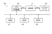
図23に、本実施形態の回路装置10を含む電子機器300の構成例を示す。この電子機器300は、本実施形態の回路装置10と、処理装置であるメインコントローラー200を含む。メインコントローラー200は第1バスBS1に接続される。例えば第1バスBS1を介してメインコントローラー200と回路装置10は接続される。また回路装置10の第2バスBS2には例えばペリフェラルデバイス260が接続される。
4). Electronic Device, Cable Harness FIG. 23 shows a configuration example of an electronic device 300 including the circuit device 10 of the present embodiment. The electronic device 300 includes the circuit device 10 of the present embodiment and a main controller 200 that is a processing device. The main controller 200 is connected to the first bus BS1. For example, the main controller 200 and the circuit device 10 are connected via the first bus BS1. Further, for example, a peripheral device 260 is connected to the second bus BS2 of the circuit device 10.

メインコントローラー200は、例えばCPU又はMPU等のプロセッサーにより実現される。或いはメインコントローラー200を各種のASICの回路装置により実現してもよい。またメインコントローラー200は、複数の回路装置(IC)や回路部品が実装された回路基板により実現されてもよい。ペリフェラルデバイス260としては、例えば図1のような携帯型端末装置250などを想定できるが、これには限定されない。ペリフェラルデバイス260はウェアラブル機器などであってもよい。   The main controller 200 is realized by a processor such as a CPU or MPU. Alternatively, the main controller 200 may be realized by various ASIC circuit devices. The main controller 200 may be realized by a circuit board on which a plurality of circuit devices (ICs) and circuit components are mounted. As the peripheral device 260, for example, a portable terminal device 250 as shown in FIG. 1 can be assumed, but the peripheral device 260 is not limited to this. The peripheral device 260 may be a wearable device or the like.

電子機器300は、記憶部310、操作部320、表示部330を更に含むことができる。記憶部310は、データを記憶するものであり、その機能はRAMやROMなどの半導体メモリーやHDD(ハードディスクドライブ)などにより実現できる。操作部320は、ユーザーが入力操作を行うためのものであり、操作ボタンやタッチパネルディスプレイをなどの操作デバイスにより実現できる。表示部330は、各種の情報を表示するものであり、液晶や有機ELなどのディスプレイにより実現できる。なお操作部320としてタッチパネルディスプレイを用いる場合には、このタッチパネルディスプレイが操作部320及び表示部330の機能を兼ねることになる。   The electronic device 300 may further include a storage unit 310, an operation unit 320, and a display unit 330. The storage unit 310 stores data, and the function can be realized by a semiconductor memory such as a RAM or a ROM, an HDD (hard disk drive), or the like. The operation unit 320 is for a user to perform an input operation, and can be realized by an operation device such as an operation button or a touch panel display. The display unit 330 displays various types of information and can be realized by a display such as a liquid crystal or an organic EL. When a touch panel display is used as the operation unit 320, the touch panel display also functions as the operation unit 320 and the display unit 330.

本実施形態により実現される電子機器300としては、例えば車載機器、印刷装置、投影装置、ロボット、頭部装着型表示装置、生体情報測定機器、距離、時間、流速又は流量等の物理量を計測する計測機器、基地局又はルーター等のネットワーク関連機器、コンテンツを配信するコンテンツ提供機器、或いはデジタルカメラ又はビデオカメラ等の映像機器などの種々の機器を想定できる。   As the electronic device 300 realized by the present embodiment, for example, an on-vehicle device, a printing device, a projection device, a robot, a head-mounted display device, a biological information measurement device, a physical quantity such as a distance, time, flow rate, or flow rate is measured. Various devices such as a measuring device, a network-related device such as a base station or a router, a content providing device that distributes content, or a video device such as a digital camera or a video camera can be assumed.

図24に本実施形態の回路装置10を含むケーブルハーネス350の構成例を示す。ケーブルハーネス350は、本実施形態の回路装置10とケーブル360を含む。ケーブル360はUSB用のケーブルである。またケーブルハーネス350はUSBレセプタクル370を含んでもよい。或いはケーブルハーネス350は図1の静電気保護回路222、短絡保護回路223などを含むものであってもよい。ケーブル360は例えば回路装置10の第2バスBS2に接続される。回路装置10の第1バスBS1側には、例えば処理装置であるメインコントローラー200等が接続される。このケーブルハーネス350は、例えば車内において配線を引き回すなどの用途に用いられる。なおケーブルハーネス350は車用以外のハーネスであってもよい。   FIG. 24 shows a configuration example of a cable harness 350 including the circuit device 10 of the present embodiment. The cable harness 350 includes the circuit device 10 and the cable 360 of the present embodiment. The cable 360 is a USB cable. The cable harness 350 may also include a USB receptacle 370. Alternatively, the cable harness 350 may include the electrostatic protection circuit 222, the short circuit protection circuit 223, and the like shown in FIG. The cable 360 is connected to the second bus BS2 of the circuit device 10, for example. For example, a main controller 200 as a processing device is connected to the first bus BS1 side of the circuit device 10. The cable harness 350 is used for applications such as routing the wiring in the vehicle, for example. The cable harness 350 may be a harness other than that for vehicles.

なお、上記のように本実施形態について詳細に説明したが、本発明の新規事項および効果から実体的に逸脱しない多くの変形が可能であることは当業者には容易に理解できるであろう。従って、このような変形例はすべて本発明の範囲に含まれるものとする。例えば、明細書又は図面において、少なくとも一度、より広義または同義な異なる用語と共に記載された用語は、明細書又は図面のいかなる箇所においても、その異なる用語に置き換えることができる。また本実施形態及び変形例の全ての組み合わせも、本発明の範囲に含まれる。また回路装置、電子機器、ケーブルハーネスの構成・動作や、バスモニター処理、バススイッチ処理、転送処理、切断検出処理、アップストリームポート検出処理等も本実施形態で説明したものに限定されず、種々の変形実施が可能である。   Although the present embodiment has been described in detail as described above, it will be easily understood by those skilled in the art that many modifications can be made without departing from the novel matters and effects of the present invention. Accordingly, all such modifications are intended to be included in the scope of the present invention. For example, a term described at least once together with a different term having a broader meaning or the same meaning in the specification or the drawings can be replaced with the different term in any part of the specification or the drawings. All combinations of the present embodiment and the modified examples are also included in the scope of the present invention. Further, the configurations and operations of circuit devices, electronic devices, cable harnesses, bus monitor processing, bus switch processing, transfer processing, disconnection detection processing, upstream port detection processing, and the like are not limited to those described in this embodiment, and various Can be implemented.

BS1…第1バス、BS2…第2バス、T1…第1期間、T2…第2期間、
PT1、PT2…ポート、LC…信号線、BSW1、BSW2…スイッチ素子、
HSD1、HSD2、HSDA、HSDB…HSドライバー、
FSD1、FSD2、FSDA、FSDB…FSドライバー、
RS11、RS12、RS21、RS22…抵抗、
RSA1、RSA2、RSB1、RSB2…抵抗、
RPU1、RPUB…プルアップ抵抗、RPDA…プルダウン抵抗、
2…ホスト、3…BCレギュレーター、4…デバイス、
8…USBレセプタクル、9…システム基板、10…回路装置、
11…第1物理層回路、12…第2物理層回路、13…基準電流回路、20…処理回路、
22…リンク層回路、24…リピーターロジック回路、30…バスモニター回路、
40…バススイッチ回路、41…第1スイッチ回路、42…第2スイッチ回路、
50…クロック信号生成回路、52…発振回路、54…PLL回路、60…電源回路、
62…レギュレーター、70…検出回路、71…電圧差判定回路、72…極性判定回路、
110…定電流回路、120…電流制御回路、
200…メインコントローラー、210…USB−HUB、
220…ケーブルハーネス、221…充電回路、222…静電気保護回路、
223…短絡保護回路、224…ケーブル、226…USBレセプタクル、
250…携帯型端末装置、260…ペリフェラルデバイス、
300…電子機器、310…記憶部、320…操作部、
350…ケーブルハーネス、360…ケーブル、370…USBレセプタクル
BS1 ... first bus, BS2 ... second bus, T1 ... first period, T2 ... second period,
PT1, PT2 ... port, LC ... signal line, BSW1, BSW2 ... switch element,
HSD1, HSD2, HSDA, HSDB ... HS driver,
FSD1, FSD2, FSDA, FSDB ... FS driver,
RS11, RS12, RS21, RS22 ... resistance,
RSA1, RSA2, RSB1, RSB2 ... resistance,
RPU1, RPUB ... pull-up resistor, RPDA ... pull-down resistor,
2 ... Host, 3 ... BC regulator, 4 ... Device,
8 ... USB receptacle, 9 ... System board, 10 ... Circuit device,
DESCRIPTION OF SYMBOLS 11 ... 1st physical layer circuit, 12 ... 2nd physical layer circuit, 13 ... Reference current circuit, 20 ... Processing circuit,
22 ... Link layer circuit, 24 ... Repeater logic circuit, 30 ... Bus monitor circuit,
40 ... bus switch circuit, 41 ... first switch circuit, 42 ... second switch circuit,
50 ... Clock signal generation circuit, 52 ... Oscillation circuit, 54 ... PLL circuit, 60 ... Power supply circuit,
62 ... Regulator, 70 ... Detection circuit, 71 ... Voltage difference determination circuit, 72 ... Polarity determination circuit,
110 ... constant current circuit, 120 ... current control circuit,
200 ... Main controller, 210 ... USB-HUB,
220 ... Cable harness, 221 ... Charging circuit, 222 ... Static protection circuit,
223 ... Short circuit protection circuit, 224 ... Cable, 226 ... USB receptacle,
250 ... portable terminal device, 260 ... peripheral device,
300 ... electronic device, 310 ... storage unit, 320 ... operation unit,
350 ... Cable harness, 360 ... Cable, 370 ... USB receptacle

Claims (14)

USB規格の第1バスが接続される第1物理層回路と、
前記USB規格の第2バスが接続される第2物理層回路と、
一端が前記第1バスに接続され、他端が前記第2バスに接続され、前記第1バスと前記第2バスとの間の接続を、第1期間においてオンにし、第2期間においてオフにするバススイッチ回路と、
前記第1バスから前記第1物理層回路を介して受信したパケットを前記第2物理層回路を介して前記第2バスに送信し、前記第2バスから前記第2物理層回路を介して受信したパケットを前記第1物理層回路を介して前記第1バスに送信する転送処理を、前記第2期間において行う処理回路と、
を含み、
前記第2物理層回路は、
前記第1物理層回路により前記第1バスにおいてホストチャープK/Jが検出されたときに、前記バススイッチ回路での前記第1バスと前記第2バスの接続がオフの状態で、前記第2バスに対してホストチャープK/Jを出力することを特徴とする回路装置。
A first physical layer circuit to which a USB standard first bus is connected;
A second physical layer circuit to which the USB standard second bus is connected;
One end is connected to the first bus, the other end is connected to the second bus, and the connection between the first bus and the second bus is turned on in the first period and turned off in the second period. A bus switch circuit to
A packet received from the first bus via the first physical layer circuit is transmitted to the second bus via the second physical layer circuit, and received from the second bus via the second physical layer circuit. A processing circuit for performing a transfer process in the second period for transmitting the transmitted packet to the first bus via the first physical layer circuit;
Including
The second physical layer circuit is
When the host chirp K / J is detected in the first bus by the first physical layer circuit, the connection between the first bus and the second bus in the bus switch circuit is off, and the second A circuit device that outputs a host chirp K / J to a bus.
請求項1において、
前記第1物理層回路は、
前記第2物理層回路により前記第2バスにおいてHSターミネーションが検出された場合に、前記第1物理層回路によるHSターミネーションをオンにすることを特徴とする回路装置。
In claim 1,
The first physical layer circuit is
A circuit device, wherein HS termination by the first physical layer circuit is turned on when HS termination is detected in the second bus by the second physical layer circuit.
請求項2において、
前記第1物理層回路は、
前記第1物理層回路による前記HSターミネーションがオフの状態で、前記第1バスにおける前記ホストチャープK/Jを検出し、前記第2物理層回路により前記第2バスにおいて前記HSターミネーションが検出された場合に、前記第1物理層回路による前記HSターミネーションをオンにすることを特徴とする回路装置。
In claim 2,
The first physical layer circuit is
The host chirp K / J in the first bus is detected in a state where the HS termination by the first physical layer circuit is off, and the HS termination is detected in the second bus by the second physical layer circuit. In the case, the circuit device is characterized in that the HS termination by the first physical layer circuit is turned on.
請求項1乃至3のいずれかにおいて、
前記第1物理層回路は、
前記第2バスにおいてデバイスチャープKが検出されたときに、前記バススイッチ回路での前記第1バスと前記第2バスの接続がオフの状態で、前記第1バスに対してデバイスチャープKを出力することを特徴とする回路装置。
In any one of Claims 1 thru | or 3,
The first physical layer circuit is
When device chirp K is detected in the second bus, device chirp K is output to the first bus in a state where the connection between the first bus and the second bus in the bus switch circuit is off A circuit device characterized by:
請求項4において、
前記バススイッチ回路での電流検出を行う検出回路を含み、
前記第1物理層回路は、
USBのバスリセット後に前記第2バスから前記バススイッチ回路を介して前記第1バスに電流が流れたことが、前記検出回路により検出されたときに、前記第1バスに対して前記デバイスチャープKを出力することを特徴とする回路装置。
In claim 4,
Including a detection circuit for performing current detection in the bus switch circuit;
The first physical layer circuit is
The device chirp K with respect to the first bus when the detection circuit detects that a current has flowed from the second bus to the first bus via the bus switch circuit after a USB bus reset. Is a circuit device.
請求項5において、
前記第2バスから前記バススイッチ回路を介して前記第1バスに電流が流れたことが、前記検出回路により検出されたときに、前記バススイッチ回路は、前記第1バスと前記第2バスの接続をオンからオフにし、前記第2物理層回路は、前記第2物理層回路によるHSターミネーションをオンにすることを特徴とする回路装置。
In claim 5,
When the detection circuit detects that a current has flowed from the second bus to the first bus via the bus switch circuit, the bus switch circuit detects whether the first bus and the second bus A circuit device, wherein connection is turned off from on, and the second physical layer circuit turns on HS termination by the second physical layer circuit.
請求項5又は6において、
前記検出回路は、
前記バスリセット後に前記第2バスから前記バススイッチ回路を介して前記第1バスに電流が流れたときに、前記第1バスがアップストリーム側のバスであり、前記第2バスがダウンストリーム側のバスであると検出し、前記バスリセット後に前記第1バスから前記バススイッチ回路を介して前記第2バスに電流が流れたときに、前記第1バスがダウンストリーム側のバスであり、前記第2バスがアップストリーム側のバスであると検出することを特徴とする回路装置。
In claim 5 or 6,
The detection circuit includes:
When a current flows from the second bus to the first bus through the bus switch circuit after the bus reset, the first bus is an upstream bus, and the second bus is a downstream bus. When a current flows from the first bus to the second bus via the bus switch circuit after the bus reset, the first bus is a downstream bus, and the first bus is a downstream bus. 2. A circuit device that detects that two buses are upstream-side buses.
請求項4乃至7のいずれかにおいて、
前記第1物理層回路は、
前記第2バスにおいて前記デバイスチャープKの出力の停止が検出されたときに、前記第1バスに対する前記デイバスチャープKの出力を停止することを特徴とする回路装置。
In any of claims 4 to 7,
The first physical layer circuit is
The circuit device, wherein when the stop of the output of the device chirp K is detected in the second bus, the output of the device chirp K to the first bus is stopped.
請求項8において、
前記第2物理層回路は、
前記第2バスでの前記デバイスチャープKの停止の後に、前記第1物理層回路により前記第1バスにおいて前記ホストチャープK/Jが検出されたときに、前記第2バスに対して前記ホストチャープK/Jを出力することを特徴とする回路装置。
In claim 8,
The second physical layer circuit is
After the stop of the device chirp K on the second bus, when the host chirp K / J is detected on the first bus by the first physical layer circuit, the host chirp with respect to the second bus A circuit device that outputs K / J.
USB規格の第1バスが接続される第1物理層回路と、
前記USB規格の第2バスが接続される第2物理層回路と、
一端が前記第1バスに接続され、他端が前記第2バスに接続され、前記第1バスと前記第2バスとの間の接続を、第1期間においてオンにし、第2期間においてオフにするバススイッチ回路と、
前記第1バスから前記第1物理層回路を介して受信したパケットを前記第2物理層回路を介して前記第2バスに送信し、前記第2バスから前記第2物理層回路を介して受信したパケットを前記第1物理層回路を介して前記第1バスに送信する転送処理を、前記第2期間において行う処理回路と、
USBのバスリセット後に前記第2バスから前記バススイッチ回路を介して前記第1バスに電流が流れたときに、前記第1バスがアップストリーム側のバスであり、前記第2バスがダウンストリーム側のバスであると検出し、前記バスリセット後に前記第1バスから前記バススイッチ回路を介して前記第2バスに電流が流れたときに、前記第1バスがダウンストリーム側のバスであり、前記第2バスがアップストリーム側のバスであると検出する検出回路と、
を含むことを特徴とする回路装置。
A first physical layer circuit to which a USB standard first bus is connected;
A second physical layer circuit to which the USB standard second bus is connected;
One end is connected to the first bus, the other end is connected to the second bus, and the connection between the first bus and the second bus is turned on in the first period and turned off in the second period. A bus switch circuit to
A packet received from the first bus via the first physical layer circuit is transmitted to the second bus via the second physical layer circuit, and received from the second bus via the second physical layer circuit. A processing circuit for performing a transfer process in the second period for transmitting the transmitted packet to the first bus via the first physical layer circuit;
When a current flows from the second bus to the first bus via the bus switch circuit after a USB bus reset, the first bus is an upstream side bus, and the second bus is a downstream side. And when a current flows from the first bus to the second bus through the bus switch circuit after the bus reset, the first bus is a downstream bus, and A detection circuit for detecting that the second bus is an upstream bus;
A circuit device comprising:
請求項10において、
前記第1物理層回路は、
前記バスリセット後に前記第2バスから前記バススイッチ回路を介して前記第1バスに電流が流れたことが、前記検出回路により検出されたときに、前記第1バスに対してデバイスチャープKを出力することを特徴とする回路装置。
In claim 10,
The first physical layer circuit is
Output device chirp K to the first bus when the detection circuit detects that a current has flowed from the second bus to the first bus via the bus switch circuit after the bus reset. A circuit device characterized by:
請求項11において、
前記第2物理層回路は、
前記第1物理層回路により前記第1バスにおいてホストチャープK/Jが検出されたときに、前前記第2バスに対してホストチャープK/Jを出力することを特徴とする回路装置。
In claim 11,
The second physical layer circuit is
A circuit device that outputs a host chirp K / J to the previous second bus when a host chirp K / J is detected on the first bus by the first physical layer circuit.
請求項1乃至12のいずれかに記載の前記回路装置と、
前記第1バスに接続される処理装置と、
を含むことを特徴とする電子機器。
The circuit device according to any one of claims 1 to 12,
A processing device connected to the first bus;
An electronic device comprising:
請求項1乃至12のいずれかに記載の前記回路装置と、
ケーブルと、
を含むことを特徴とするケーブルハーネス。
The circuit device according to any one of claims 1 to 12,
Cable and
Cable harness characterized by including.
JP2018065199A 2018-03-29 2018-03-29 Circuit device, electronic apparatus and cable harness Pending JP2019175308A (en)

Priority Applications (3)

Application Number Priority Date Filing Date Title
JP2018065199A JP2019175308A (en) 2018-03-29 2018-03-29 Circuit device, electronic apparatus and cable harness
CN201910235823.5A CN110321311B (en) 2018-03-29 2019-03-27 Circuit device, electronic apparatus, and cable harness
US16/367,485 US10509756B2 (en) 2018-03-29 2019-03-28 Circuit device, electronic device, and cable harness

Applications Claiming Priority (1)

Application Number Priority Date Filing Date Title
JP2018065199A JP2019175308A (en) 2018-03-29 2018-03-29 Circuit device, electronic apparatus and cable harness

Publications (1)

Publication Number Publication Date
JP2019175308A true JP2019175308A (en) 2019-10-10

Family

ID=68057070

Family Applications (1)

Application Number Title Priority Date Filing Date
JP2018065199A Pending JP2019175308A (en) 2018-03-29 2018-03-29 Circuit device, electronic apparatus and cable harness

Country Status (3)

Country Link
US (1) US10509756B2 (en)
JP (1) JP2019175308A (en)
CN (1) CN110321311B (en)

Families Citing this family (3)

* Cited by examiner, † Cited by third party
Publication number Priority date Publication date Assignee Title
US11176071B2 (en) * 2018-11-09 2021-11-16 Cypress Semiconductor Corporation USB signal switch circuitry using standard USB hub and method of operation the same
US11309892B2 (en) * 2020-02-12 2022-04-19 Texas Instruments Incorporated Data bus signal conditioner and level shifter
JP2022021594A (en) * 2020-07-22 2022-02-03 セイコーエプソン株式会社 Circuit device, electronic apparatus, and mobile body

Family Cites Families (14)

* Cited by examiner, † Cited by third party
Publication number Priority date Publication date Assignee Title
JP3587162B2 (en) * 2000-10-31 2004-11-10 セイコーエプソン株式会社 Data transfer control device and electronic equipment
WO2004061636A1 (en) * 2002-12-27 2004-07-22 Fujitsu Limited Usb device and method for controlling usb device
JP2006135397A (en) 2004-11-02 2006-05-25 Seiko Epson Corp Data transfer controller and electronic equipment
TW200707208A (en) * 2005-08-03 2007-02-16 Sunplus Technology Co Ltd USB device capable of automatically detecting USB mode and method thereof
US7966502B2 (en) * 2007-12-20 2011-06-21 Broadcom Corporation System and method for enabling power over ethernet for legacy devices
TW200931422A (en) * 2008-01-04 2009-07-16 Afa Technologies Inc A high-speed flash memory storage device
TWI533138B (en) * 2009-05-19 2016-05-11 慧榮科技股份有限公司 Signal generating apparatus and signal generating method
JP2011215855A (en) * 2010-03-31 2011-10-27 Renesas Electronics Corp Usb device control circuit and control method of usb device
CN102541798B (en) * 2010-12-07 2015-06-10 瑞昱半导体股份有限公司 Online correction method and device of general serial bus system
US9817772B2 (en) * 2012-12-20 2017-11-14 Icron Technologies Corporation Systems and methods for exchanging USB information with selected remote devices
US10268618B2 (en) * 2015-04-16 2019-04-23 Advanced Micro Devices, Inc. Chip level switching for multiple computing device interfaces
US20170168979A1 (en) * 2015-12-09 2017-06-15 Qualcomm Incorporated Capacitively coupling differential data lines of a usb2 physical layer interface transceiver (phy) to one or more components of a high speed module in response to a transition of the phy into high speed mode
US10120436B2 (en) * 2016-03-23 2018-11-06 Intel Corporation Apparatuses, systems, and methods for USB high-speed chirp detection
TWI781134B (en) * 2017-01-25 2022-10-21 日商精工愛普生股份有限公司 Circuit device, electronic device, and cable harness

Also Published As

Publication number Publication date
US20190303331A1 (en) 2019-10-03
US10509756B2 (en) 2019-12-17
CN110321311A (en) 2019-10-11
CN110321311B (en) 2023-04-25

Similar Documents

Publication Publication Date Title
US11368332B2 (en) Circuit device, electronic device, and cable harness
US8045626B2 (en) Differential transmitter, differential receiver, signal transmitter, and signal transmitting system
US7249271B2 (en) Data transfer control device and electronic instrument
US9484921B2 (en) LVDS input circuit with comparators, or gate, and multiplexer
CN110321311B (en) Circuit device, electronic apparatus, and cable harness
US11128487B2 (en) Circuit device, electronic device, and mobile body
CN112732608B (en) Circuit device, electronic apparatus, and moving object
US11030138B2 (en) Circuit device, electronic device, and cable harness
US11416438B2 (en) Circuit device, electronic device, cable harness, and data transfer method
JP2019041346A (en) Transmission circuit, integrated circuit device, and electronic equipment
CN110622011B (en) Repeater for open-drain communication system
CN110321308B (en) Circuit device, electronic apparatus, and cable harness
JP6950187B2 (en) Circuit equipment, electronic devices and cable harnesses
JP6900780B2 (en) Circuit equipment, electronic devices and cable harnesses
US20220224335A1 (en) Data bus signal conditioner and level shifter
JP6904210B2 (en) Circuit equipment, electronic devices and cable harnesses