JP2017537588A - converter - Google Patents
converter Download PDFInfo
- Publication number
- JP2017537588A JP2017537588A JP2017522037A JP2017522037A JP2017537588A JP 2017537588 A JP2017537588 A JP 2017537588A JP 2017522037 A JP2017522037 A JP 2017522037A JP 2017522037 A JP2017522037 A JP 2017522037A JP 2017537588 A JP2017537588 A JP 2017537588A
- Authority
- JP
- Japan
- Prior art keywords
- switch
- power receiver
- voltage
- power
- state
- Prior art date
- Legal status (The legal status is an assumption and is not a legal conclusion. Google has not performed a legal analysis and makes no representation as to the accuracy of the status listed.)
- Pending
Links
Images


Classifications
-
- H—ELECTRICITY
- H02—GENERATION; CONVERSION OR DISTRIBUTION OF ELECTRIC POWER
- H02J—CIRCUIT ARRANGEMENTS OR SYSTEMS FOR SUPPLYING OR DISTRIBUTING ELECTRIC POWER; SYSTEMS FOR STORING ELECTRIC ENERGY
- H02J50/00—Circuit arrangements or systems for wireless supply or distribution of electric power
- H02J50/10—Circuit arrangements or systems for wireless supply or distribution of electric power using inductive coupling
- H02J50/12—Circuit arrangements or systems for wireless supply or distribution of electric power using inductive coupling of the resonant type
-
- H—ELECTRICITY
- H02—GENERATION; CONVERSION OR DISTRIBUTION OF ELECTRIC POWER
- H02M—APPARATUS FOR CONVERSION BETWEEN AC AND AC, BETWEEN AC AND DC, OR BETWEEN DC AND DC, AND FOR USE WITH MAINS OR SIMILAR POWER SUPPLY SYSTEMS; CONVERSION OF DC OR AC INPUT POWER INTO SURGE OUTPUT POWER; CONTROL OR REGULATION THEREOF
- H02M3/00—Conversion of dc power input into dc power output
- H02M3/22—Conversion of dc power input into dc power output with intermediate conversion into ac
- H02M3/24—Conversion of dc power input into dc power output with intermediate conversion into ac by static converters
- H02M3/28—Conversion of dc power input into dc power output with intermediate conversion into ac by static converters using discharge tubes with control electrode or semiconductor devices with control electrode to produce the intermediate ac
- H02M3/325—Conversion of dc power input into dc power output with intermediate conversion into ac by static converters using discharge tubes with control electrode or semiconductor devices with control electrode to produce the intermediate ac using devices of a triode or a transistor type requiring continuous application of a control signal
- H02M3/335—Conversion of dc power input into dc power output with intermediate conversion into ac by static converters using discharge tubes with control electrode or semiconductor devices with control electrode to produce the intermediate ac using devices of a triode or a transistor type requiring continuous application of a control signal using semiconductor devices only
- H02M3/33569—Conversion of dc power input into dc power output with intermediate conversion into ac by static converters using discharge tubes with control electrode or semiconductor devices with control electrode to produce the intermediate ac using devices of a triode or a transistor type requiring continuous application of a control signal using semiconductor devices only having several active switching elements
- H02M3/33576—Conversion of dc power input into dc power output with intermediate conversion into ac by static converters using discharge tubes with control electrode or semiconductor devices with control electrode to produce the intermediate ac using devices of a triode or a transistor type requiring continuous application of a control signal using semiconductor devices only having several active switching elements having at least one active switching element at the secondary side of an isolation transformer
- H02M3/33592—Conversion of dc power input into dc power output with intermediate conversion into ac by static converters using discharge tubes with control electrode or semiconductor devices with control electrode to produce the intermediate ac using devices of a triode or a transistor type requiring continuous application of a control signal using semiconductor devices only having several active switching elements having at least one active switching element at the secondary side of an isolation transformer having a synchronous rectifier circuit or a synchronous freewheeling circuit at the secondary side of an isolation transformer
-
- H—ELECTRICITY
- H02—GENERATION; CONVERSION OR DISTRIBUTION OF ELECTRIC POWER
- H02M—APPARATUS FOR CONVERSION BETWEEN AC AND AC, BETWEEN AC AND DC, OR BETWEEN DC AND DC, AND FOR USE WITH MAINS OR SIMILAR POWER SUPPLY SYSTEMS; CONVERSION OF DC OR AC INPUT POWER INTO SURGE OUTPUT POWER; CONTROL OR REGULATION THEREOF
- H02M7/00—Conversion of ac power input into dc power output; Conversion of dc power input into ac power output
- H02M7/02—Conversion of ac power input into dc power output without possibility of reversal
- H02M7/04—Conversion of ac power input into dc power output without possibility of reversal by static converters
- H02M7/12—Conversion of ac power input into dc power output without possibility of reversal by static converters using discharge tubes with control electrode or semiconductor devices with control electrode
- H02M7/21—Conversion of ac power input into dc power output without possibility of reversal by static converters using discharge tubes with control electrode or semiconductor devices with control electrode using devices of a triode or transistor type requiring continuous application of a control signal
- H02M7/217—Conversion of ac power input into dc power output without possibility of reversal by static converters using discharge tubes with control electrode or semiconductor devices with control electrode using devices of a triode or transistor type requiring continuous application of a control signal using semiconductor devices only
- H02M7/219—Conversion of ac power input into dc power output without possibility of reversal by static converters using discharge tubes with control electrode or semiconductor devices with control electrode using devices of a triode or transistor type requiring continuous application of a control signal using semiconductor devices only in a bridge configuration
- H02M7/2195—Conversion of ac power input into dc power output without possibility of reversal by static converters using discharge tubes with control electrode or semiconductor devices with control electrode using devices of a triode or transistor type requiring continuous application of a control signal using semiconductor devices only in a bridge configuration the switches being synchronously commutated at the same frequency of the AC input voltage
-
- H—ELECTRICITY
- H02—GENERATION; CONVERSION OR DISTRIBUTION OF ELECTRIC POWER
- H02M—APPARATUS FOR CONVERSION BETWEEN AC AND AC, BETWEEN AC AND DC, OR BETWEEN DC AND DC, AND FOR USE WITH MAINS OR SIMILAR POWER SUPPLY SYSTEMS; CONVERSION OF DC OR AC INPUT POWER INTO SURGE OUTPUT POWER; CONTROL OR REGULATION THEREOF
- H02M7/00—Conversion of ac power input into dc power output; Conversion of dc power input into ac power output
- H02M7/42—Conversion of dc power input into ac power output without possibility of reversal
- H02M7/44—Conversion of dc power input into ac power output without possibility of reversal by static converters
- H02M7/48—Conversion of dc power input into ac power output without possibility of reversal by static converters using discharge tubes with control electrode or semiconductor devices with control electrode
- H02M7/53—Conversion of dc power input into ac power output without possibility of reversal by static converters using discharge tubes with control electrode or semiconductor devices with control electrode using devices of a triode or transistor type requiring continuous application of a control signal
- H02M7/537—Conversion of dc power input into ac power output without possibility of reversal by static converters using discharge tubes with control electrode or semiconductor devices with control electrode using devices of a triode or transistor type requiring continuous application of a control signal using semiconductor devices only, e.g. single switched pulse inverters
- H02M7/5387—Conversion of dc power input into ac power output without possibility of reversal by static converters using discharge tubes with control electrode or semiconductor devices with control electrode using devices of a triode or transistor type requiring continuous application of a control signal using semiconductor devices only, e.g. single switched pulse inverters in a bridge configuration
- H02M7/53871—Conversion of dc power input into ac power output without possibility of reversal by static converters using discharge tubes with control electrode or semiconductor devices with control electrode using devices of a triode or transistor type requiring continuous application of a control signal using semiconductor devices only, e.g. single switched pulse inverters in a bridge configuration with automatic control of output voltage or current
- H02M7/53878—Conversion of dc power input into ac power output without possibility of reversal by static converters using discharge tubes with control electrode or semiconductor devices with control electrode using devices of a triode or transistor type requiring continuous application of a control signal using semiconductor devices only, e.g. single switched pulse inverters in a bridge configuration with automatic control of output voltage or current by time shifting switching signals of one diagonal pair of the bridge with respect to the other diagonal pair
-
- Y—GENERAL TAGGING OF NEW TECHNOLOGICAL DEVELOPMENTS; GENERAL TAGGING OF CROSS-SECTIONAL TECHNOLOGIES SPANNING OVER SEVERAL SECTIONS OF THE IPC; TECHNICAL SUBJECTS COVERED BY FORMER USPC CROSS-REFERENCE ART COLLECTIONS [XRACs] AND DIGESTS
- Y02—TECHNOLOGIES OR APPLICATIONS FOR MITIGATION OR ADAPTATION AGAINST CLIMATE CHANGE
- Y02B—CLIMATE CHANGE MITIGATION TECHNOLOGIES RELATED TO BUILDINGS, e.g. HOUSING, HOUSE APPLIANCES OR RELATED END-USER APPLICATIONS
- Y02B70/00—Technologies for an efficient end-user side electric power management and consumption
- Y02B70/10—Technologies improving the efficiency by using switched-mode power supplies [SMPS], i.e. efficient power electronics conversion e.g. power factor correction or reduction of losses in power supplies or efficient standby modes
Abstract
共振回路(802)を介して接続された少なくとも2つのスイッチS1,S2を備える誘導受電器(3)であって、当該共振回路は、インダクタンス及びキャパシタンスを含み、当該少なくとも2つのスイッチのうちの第1スイッチS1は、受電器変数に依存した第1イベントに基づいて第1状態に切り替わるように構成され、当該第1スイッチは、受電器変数に依存しない第2イベントに基づいて第2状態に切り替わるように構成されている。An inductive power receiver (3) comprising at least two switches S1, S2 connected via a resonant circuit (802), the resonant circuit including an inductance and a capacitance, the first of the at least two switches. The one switch S1 is configured to switch to the first state based on a first event that depends on the power receiver variable, and the first switch switches to the second state based on a second event that does not depend on the power receiver variable. It is configured as follows.
Description
本発明は、概して、コンバータに関し、限定するものではないが、特に、誘導電力伝送システム用のコンバータに関する。 The present invention relates generally to converters, and more particularly, but not exclusively, to converters for inductive power transfer systems.
電気コンバータは、技術的に周知であり、種々の応用についての多くの構成において利用可能である。一般的に、コンバータは、1つのタイプの電気供給を異なるタイプの出力に変換する。このような変換には、DC−DC、AC−AC及びDC−AC電気変換が含まれうる。いくつかの構成では、コンバータは、任意の数のDC及びAC「部品」を有し、例えば、DC−DCコンバータは、AC−ACトランス・コンバータ部を内蔵しうる。 Electrical converters are well known in the art and are available in many configurations for various applications. In general, a converter converts one type of electrical supply to a different type of output. Such conversion may include DC-DC, AC-AC and DC-AC electrical conversion. In some configurations, the converter has any number of DC and AC “components”, for example, the DC-DC converter may incorporate an AC-AC transformer converter section.
より具体的には、「インバータ」は、DC−ACコンバータを表すために使用されうる用語である。インバータは、より大きなコンバータと分離して又はその一部として存在しうる(上記の例のように、AC−ACトランスの前段でDCをACに変換しなければならない)。このため、「コンバータ」は、インバータ自体と、インバータを含むコンバータとを包含するように解釈されるべきである。明確化のために、本明細書の残りの部分では、インバータがある文脈における適切な代替用語でありうる可能性を除外することなく、「コンバータ」にのみ言及する。 More specifically, “inverter” is a term that can be used to represent a DC-AC converter. The inverter can exist separately from or as part of a larger converter (as in the above example, DC must be converted to AC before the AC-AC transformer). For this reason, a “converter” should be construed to encompass the inverter itself and the converter that includes the inverter. For clarity, the remainder of this specification refers only to “converters” without excluding the possibility that an inverter may be a suitable alternative term in a context.
DC−AC変換を実現するコンバータについての多数の構成が存在する。主に、これは、調整されたスイッチングによって、交互に切り替わる方向に電流が素子を流れるようにするスイッチの適切な配置を通して実現される。当該スイッチは、所望のAC出力波形を実現するように、制御回路によって制御されうる。出力波形を形成するために、追加の回路素子が含まれてもよい。特定の回路トポロジーの影響を受けて、出力波形が、スイッチの周波数、デューティサイクル、及び機能相互関係に依存することになる。 There are numerous configurations for converters that implement DC-AC conversion. Primarily, this is achieved through a suitable arrangement of switches that allow the current to flow through the device in alternating directions with tuned switching. The switch can be controlled by a control circuit to achieve a desired AC output waveform. Additional circuit elements may be included to form the output waveform. Under the influence of a particular circuit topology, the output waveform will depend on the switch frequency, duty cycle, and functional interrelationship.
コンバータの使用の一例は、誘導電力伝送(IPT)システムとの関連である。これらのシステムは、確立された技術(例えば、電気歯ブラシの無線充電)及び開発中の技術(例えば、「充電マット」上でのハンドヘルドデバイスの無線充電)の周知の領域である。典型的には、一次側は、送信コイル又は複数の送信コイルから時変の磁界を発生させる。この磁界は、適切な受信コイルに交流電流を誘導し、それにより、当該受信コイルは、バッテリーを充電するために、又はデバイス若しくは他の負荷に電力を供給するために使用されうる。いくつかの例では、共振回路を作るために送信コイルの周囲にコンデンサを追加できる。同様に、共振回路を作るために(複数の)受信コイルの周囲にコンデンサが追加されうる。共振回路の使用により、対応する共振周波数において電力スループット及び効率が増大しうる。 One example of the use of a converter is in connection with an inductive power transfer (IPT) system. These systems are well known areas of established technology (eg, wireless charging of electric toothbrushes) and technology under development (eg, wireless charging of handheld devices on a “charging mat”). Typically, the primary side generates a time-varying magnetic field from the transmitter coil or transmitter coils. This magnetic field induces an alternating current in a suitable receiver coil, so that the receiver coil can be used to charge a battery or power a device or other load. In some examples, a capacitor can be added around the transmit coil to create a resonant circuit. Similarly, a capacitor can be added around the receiver coil (s) to create a resonant circuit. The use of a resonant circuit can increase power throughput and efficiency at the corresponding resonant frequency.
通常、送信コイルは、コンバータによって駆動される。駆動回路の特性(例えば、周波数、位相、及び振幅)は、特定のIPTシステムに関係することになる。いくつかの例では、コンバータの駆動周波数は、共振送信コイル及び/又は共振受信コイルの共振周波数と一致することが望ましい場合がある。その振幅は、二次側の負荷の要求条件に対応するように変更されうる。いくつかのシステムでは、負荷の要求条件が、適切な手段によって一次側へ伝達されうる。 Usually, the transmission coil is driven by a converter. The characteristics of the drive circuit (eg, frequency, phase, and amplitude) will be related to the particular IPT system. In some examples, it may be desirable for the drive frequency of the converter to match the resonant frequency of the resonant transmit coil and / or the resonant receive coil. The amplitude can be changed to correspond to the secondary load requirements. In some systems, load requirements can be communicated to the primary by appropriate means.
これらの制御の積み重ねの全ては、IPTシステムの設計に複雑性及びコストをもたらす。このため、コンバータを制御する簡略化した方法があることが望まれる。 All of these control stacks add complexity and cost to the design of an IPT system. For this reason, it is desirable to have a simplified method of controlling the converter.
IPTシステムに関連する他の問題は、共振システムでは送電器の共振周波数が固定されておらず、受電器の負荷に応じて変化することである。負荷の変化は、相互誘導結合を介して送電器へ逆に反映され、これは送電器の共振周波数に影響する。このため、コンバータが、もはや送電器の共振周波数と等しくない周波数で送信コイルへ出力を供給している場合、電力スループットが減少し、システムの効率が低くなる。 Another problem associated with IPT systems is that in resonant systems, the resonant frequency of the power transmitter is not fixed and varies with the load on the power receiver. The change in load is reflected back to the transmitter via mutual inductive coupling, which affects the resonant frequency of the transmitter. Thus, if the converter is no longer supplying power to the transmit coil at a frequency that is not equal to the transmitter's resonant frequency, power throughput is reduced and system efficiency is reduced.
IPTシステムに関連する更なる問題は、送信又は受信コイル及び共振コンデンサのような共振素子の値が、製造公差、年代、温度、送電距離の変化、及び近くの金属又は磁性物質、その他の要因に起因して、変化しうることである。このような変化は、送電器の共振周波数に影響し、当該共振周波数が受電器との共振から外れる可能性があり、それにより、電力スループットが減少し、システムの効率が低くなる。 A further problem associated with IPT systems is that the values of resonant elements, such as transmit or receive coils and resonant capacitors, depend on manufacturing tolerances, age, temperature, changes in transmission distance, and nearby metals or magnetic materials, and other factors. It can be changed. Such changes affect the resonant frequency of the power transmitter, which can deviate from resonance with the power receiver, thereby reducing power throughput and reducing system efficiency.
共振周波数のこのような変化に対応する1つの方法は、送信コイルの両端電圧が0になった際にオフとオフとが切り替わるように制御スイッチを適応させることによるものである。これにより、切り替え(スイッチング)周波数は自動的に送信コイルの共振周波数に対応することになる。このような解決策の欠点は、それにより送信磁界の周波数が送信コイルの共振周波数に依存した範囲にわたって変化することである。これは、2つの理由で問題があり、第1は、受電器が、送信周波数の変化に対して適応的に再チューニングしなければならないこと、あるいは電力を失うことであり、第2は、利用可能な帯域幅が狭すぎる可能性があるため、周波数範囲にわたってシステムを動作させることが望ましくないことである。 One way to deal with such a change in resonant frequency is by adapting the control switch to switch off and off when the voltage across the transmission coil becomes zero. As a result, the switching frequency automatically corresponds to the resonance frequency of the transmission coil. The disadvantage of such a solution is that it changes the frequency of the transmitted magnetic field over a range that depends on the resonant frequency of the transmit coil. This is problematic for two reasons: the first is that the power receiver has to adaptively retune or change power to changes in the transmission frequency, and the second is the utilization. It is not desirable to operate the system over the frequency range because the possible bandwidth may be too narrow.
本発明の目的は、有用な選択肢を公に提供することにある。 The object of the present invention is to publicly provide useful options.
一実施形態によれば、共振回路を介して接続された少なくとも2つのスイッチを備える誘導受電器であって、前記共振回路は、インダクタンス及びキャパシタンスを含み、
前記少なくとも2つのスイッチのうちの第1スイッチは、受電器変数に依存した第1イベントに基づいて第1状態に切り替わるように構成され、
前記第1スイッチは、受電器変数に依存しない第2イベントに基づいて第2状態に切り替わるように構成されている、受電器が提供される。
According to one embodiment, an inductive power receiver comprising at least two switches connected via a resonant circuit, the resonant circuit comprising an inductance and a capacitance;
A first switch of the at least two switches is configured to switch to a first state based on a first event dependent on a receiver variable;
A power receiver is provided, wherein the first switch is configured to switch to a second state based on a second event that does not depend on a power receiver variable.
用語「comprise(含む、備える)」、「comprises(含む、備える)」及び「comprising(含む、備える)」は、様々な司法権の下で、排他的または包含的な意味で用いられうるものと認められる。本明細書のために、これらの用語は、特に言及されない限り包含的な意味を有することが意図されており、即ち、それらは、直接的に参照を使用する、記載された構成要素を含むこと、及び特定されていない他の構成要素または要素も含みうることを意味するものとされる。 The terms “comprise”, “comprises” and “comprising” may be used in an exclusive or inclusive sense under various jurisdictions. Is recognized. For the purposes of this specification, these terms are intended to have an inclusive meaning unless otherwise noted, that is, they include the components described using direct reference. , And other components or elements not specified are meant to be included.
そのような先行技術が共通の一般知識の一部を形成することの承認を形成するものではない。 It does not form an admission that such prior art forms part of common general knowledge.
本明細書に組み込まれ、本明細書の一部を構成する添付の図面は、本発明の実施形態を示しており、また、上記で与えられた本発明の概要、及び以下で与えられる実施形態の詳細な説明とともに、本発明の原理を説明するのに貢献する。 The accompanying drawings, which are incorporated in and constitute a part of this specification, illustrate embodiments of the present invention and also provide an overview of the invention given above and the embodiments given below. Together with a detailed description of the present invention contributes to the description of the principles of the present invention.
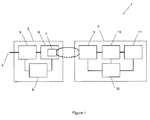
図1には、誘導電力伝送(IPT)システム1が大まかに示されている。IPTシステムは、誘導送電器2及び誘導受電器3を備える。誘導送電器は、適切な電源4(主電源等)に接続される。誘導送電器は、インバータ6に接続されたAC−DCコンバータ5を備えうる。インバータは、送信コイル又は複数の送信コイル7が交流磁界を生成するよう、当該送信コイル又は複数の送信コイルへAC電流を供給する。いくつかの構成では、送信コイルは、インバータから分離されていると考えられてもよい。送信コイル又は複数の送信コイルは、共振回路を作るために、コンデンサ(図示せず)に並列又は直列に接続されてもよい。
FIG. 1 schematically shows an inductive power transmission (IPT)
図1は、誘導送電器2内のコントローラ8も示している。コントローラは、誘導送電器の各部に接続されうる。コントローラは、誘導送電器の各部からの入力を受信して、各部の動作を制御する出力を生成するよう構成されうる。コントローラは、単一のユニット又は個別のユニットとして実装され、例えば、電力フロー、チューニング、送信コイルへの選択的な通電、誘導受電器の検出、及び/又は通信を含む、誘導送電器の能力に依存して、当該誘導送電器の種々の態様を制御するよう構成されうる。
FIG. 1 also shows a
誘導受電器3は、負荷11へ電力を供給する受信回路10に接続された、受信コイル又は複数の受信コイル9を備える。誘導送電器2及び誘導受電器3が適切に結合されている場合、送信コイル又は複数の送信コイル7によって生成される交流磁界が、受信コイル又は複数の受信コイル9に交流電流を誘導する。受信回路10は、誘導電流を、負荷11に適した形式に変換するように構成される。受信コイル又は複数の受信コイル9は、共振回路を作るために、コンデンサ(図示せず)に並列又は直列に接続されてもよい。いくつかの誘導受電器において、当該受電器は、受信コイル又は複数の受信コイル9のチューニングを制御、又は受信回路10によって負荷11へ供給される電力を制御しうるコントローラ12を備えうる。
The
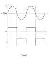
図2は、インバータ6の例を示す。インバータ6は、DC電源202、DCインダクタ203、出力インダクタ204(送信コイル7)、共振コンデンサ205、(明確化のため、スイッチ1 206及びスイッチ2 207と称される)制御スイッチ、及び制御回路208を備える。図2には、制御スイッチの特徴である寄生コンデンサ209及び寄生ボディダイオード210も示されている。
FIG. 2 shows an example of the inverter 6. The inverter 6 includes a
インバータ6の典型的な動作の下では、スイッチ1 206及びスイッチ2 207は、50%のデューティサイクルで交互にオン及びオフに切り替えられる。当該切り替えの周波数は、出力インダクタ204及び共振コンデンサ205の本来の共振周波数に一致するものである。これにより、図3に示されるような波形が生成されることになる。当該切り替えパターンを実現するために、従前のシステムは、出力インダクタの電圧のゼロクロスに応じて交互にスイッチをアクティブ化するようプログラムされたコントローラを採用していた場合がある。
Under typical operation of inverter 6,
コンバータを制御する方法は、以下のとおりであり、即ち、各スイッチが、コンバータ変数に依存した第1切り替えイベントが発生した際に第1状態へ切り替えられ、コンバータ変数に依存しない第2切り替えイベントが発生した際に第2状態へ切り替えられる。 The method of controlling the converter is as follows: each switch is switched to the first state when a first switching event dependent on the converter variable occurs, and a second switching event independent of the converter variable is generated. When it occurs, it is switched to the second state.
以下では、第1状態をオン状態と称し、第2状態をオフ状態と称する。しかし、第1状態がオフ状態であってもよく、第2状態がオン状態であってもよい。 Hereinafter, the first state is referred to as an on state, and the second state is referred to as an off state. However, the first state may be an off state, and the second state may be an on state.
<第1切り替えイベント>
第1切り替えイベントは、スイッチ1 206又はスイッチ2 207の両端電圧が0又は0付近に達した場合である。即ち、スイッチ1は、当該スイッチの両端電圧が0又は0付近に達すると、オンに切り替わり、スイッチ2は、当該スイッチ2の両端電圧が0又は0付近に達すると、オンに切り替わる。スイッチ1 206又はスイッチ2 207の両端電圧は、出力インダクタ204の両端電圧に依存するため、コンバータに依存する変数に関係していると言えよう。第1切り替えイベントの発生がシステムの変化に伴って変わりうるため、当該スイッチのオンへの切り替えは当該システムの変化に対応しうる。
<First switching event>
The first switching event is when the voltage across the
このように、第1イベントは、コンバータ変数に依存し、当該コンバータ変数は、電圧のゼロクロスである。 Thus, the first event depends on the converter variable, which is a zero crossing of the voltage.
当該電圧は検出可能であり、ある値に達すると、トリガ・イベントになる。例えば、共振送信コイルの両端電圧が、規定された閾値を下回った場合に、比較回路が状態の変化を出力してもよい。この制御は、制御回路208に含まれうる。
The voltage can be detected, and when it reaches a certain value, it becomes a trigger event. For example, the comparison circuit may output a change in state when the voltage across the resonant transmission coil falls below a prescribed threshold. This control can be included in the
スイッチ1 206又はスイッチ2 207の両端電圧が0に到達した又は近づいたことを、第1切り替えイベントとして使用することの1つの利点は、ゼロ電圧切り替えでありうる。即ち、スイッチは、当該スイッチの両端電圧が0になるとオンに切り替えられ、これは、エネルギー損失を最小限にし、効率を改善し、かつ、過電流に起因したスイッチへのダメージを防止する。
One advantage of using as the first switching event that the voltage across
他の実施形態では、第1切り替えイベントは、スイッチ1又はスイッチ2を流れる電流のゼロクロスである。即ち、スイッチ1は、スイッチ1を流れる電流が0又は0付近に達すると、オンに切り替わり、スイッチ2は、スイッチ2を流れる電流が0又は0付近に達すると、オンに切り替わる。システム1の他の変数の特徴が、第1切り替えイベントの基礎として適していてもよい。
In other embodiments, the first switching event is a zero crossing of the current flowing through
<第2切り替えイベント>
第2切り替えイベントは、他のスイッチがオフに切り替わってからの一定時間間隔(α)の満了である。即ち、スイッチ1 206は、スイッチ2がオフに切り替わってから一定時間間隔(α)でオフに切り替わり、スイッチ2 207は、スイッチ1がオフに切り替わってから一定時間間隔(α)でオフに切り替わる。スイッチ1又はスイッチ2のオフへの切り替えは、システムに依存ずる関係しない(即ち、プリセットされており、変化しない)ため、システムのいかなる変化にもかかわらず同じままである。更に、スイッチは、一定時間間隔の後に継続的にオフに切り替わるため、スイッチの周波数も、システムに依存する変数に関係しない。コンバータの周波数は、式1によって計算されうる。
fconverter=1/(2α) (1)
<Second switching event>
The second switching event is the expiration of a certain time interval (α) after the other switch is turned off. That is, the
f converter = 1 / (2α) (1)
スイッチのオフ状態への切り替えを検出するための、及び一定遅延の後に他のスイッチのオフへの切り替えをトリガするための回路が含まれうる。あるいは、スイッチの状態の変化を実際に検出する必要なく、このプロセスを内部的に制御するよう、コントローラがプログラムされうる。この制御は、制御回路208に含まれてもよく、時間間隔αは、ユーザによって又はルックアップテーブルに従って変更されてもよい。
Circuitry can be included for detecting the switch-off state and for triggering the switch-off of another switch after a certain delay. Alternatively, the controller can be programmed to control this process internally without having to actually detect a change in the state of the switch. This control may be included in the
このように、第2イベントは、コンバータ変数に依存せず、遅延αは、コンバータの動作変数(例えば、電圧又は電流ベースの変数)に依存せずに設定され、当該第2イベントは、遅延の終わり(conclusion)である。 Thus, the second event does not depend on the converter variable, and the delay α is set independently of the converter operating variable (eg, voltage or current based variable), and the second event It is the conclusion.
あるいは、第2切り替えイベントは、同じスイッチの状態の変化から始まる時間間隔の満了であってもよいし、又は、スイッチのオフへの切り替えを他のスイッチの状態に関係なくトリガするために、クロック信号が使用されてもよい。 Alternatively, the second switching event may be the expiration of a time interval starting from the same switch state change, or a clock to trigger a switch-off switch regardless of the state of the other switch. A signal may be used.
図4は、スイッチ1及びスイッチ2の状態、各スイッチの両端電圧、及び出力インダクタの両端電圧を示している。時刻t1において、スイッチ1がオフに切り替わり、スイッチ2がオンに切り替わる。スイッチ2は、当該スイッチの両端電圧が0に達するため、オンに切り替わる。スイッチ1がオフに切り替わるため、インダクタの両端電圧は、増加し始め、その後、減少し始める(観測されている波形が得られる)。スイッチ1がオフに切り替わってから時間αの経過後の、時刻t2において、スイッチ2がオフに切り替わる。αは、出力インダクタ及び出力コンデンサの本来の共振期間の半分(tR)に一致するようにプリセットされており、かつ、t2は、スイッチ1の両端電圧が0に達する時刻に相当するため、スイッチ1がオンに切り替わる。このサイクルが繰り返され、上述の一定周波数を有する50%のデューティサイクルと同様の効果を有する切り替えパターンが得られる。
FIG. 4 shows the states of the
場合によっては、出力インダクタ及び出力コンデンサの共振周波数は、例えば、回路部品の劣化、IPTシステムにおける一次コイルと二次コイルとの間の結合に影響する負荷の変化等に起因して変化しうる。図5は、共振期間の半分(tR')がαより小さい場合、又はαがtR'より大きい値に固定されている場合を示している。時刻t1において、スイッチ1がオフに切り替わり、それにより、インダクタの両端電圧が増加して、その後、減少することで、観測されている波形が得られる。tR'がαより小さいため、スイッチ1の両端電圧は、αが経過する前に0に到達する。それ故に、t2において、スイッチ1がオンに切り替わる。これは、スイッチ2がオフに切り替わる前に発生し、それにより、両方のスイッチが同時にオンになる。その後、スイッチ1がオフに切り替わってから時間αの経過後の、時刻t3において、スイッチ2がオフに切り替わる。このサイクルが繰り返され、50%より大きいが、図3に示される例と同じ周波数(即ち、1/(2α))を有するデューティサイクルの、切り替えパターンが得られる。
In some cases, the resonant frequencies of the output inductor and output capacitor may change due to, for example, circuit component degradation, load changes that affect the coupling between the primary and secondary coils in the IPT system, and the like. FIG. 5 shows a case where half of the resonance period (t R ′) is smaller than α, or α is fixed to a value larger than t R ′. At time t 1 , the
図6は、tR''がαより大きい場合(又は等価的には、αがtR''より小さく設定されている場合)を示している。この実施形態では、各サイクルの一部において両方のスイッチが(図4で与えられる例のように)同時にオンになるのではなく、両方のスイッチが同時にオフになる。 FIG. 6 shows a case where t R ″ is larger than α (or equivalently, α is set smaller than t R ″). In this embodiment, instead of turning both switches on at the same time (as in the example given in FIG. 4) in part of each cycle, both switches are turned off at the same time.
インダクタ203に蓄積されたエネルギーに起因して、オープンのスイッチ1 206又はオープンのスイッチ2 207の両端間に高電圧スパイクが生じることを避けるために、スナバ(snubber)ネットワークが使用されうる。例えば、追加の離散コンデンサが、スイッチ1 206及びスイッチ2 207のそれぞれの両端間にスナバとして設けられうるとともに、出力インダクタ204と一緒に共振ネットワークの一部を形成しうる。
To avoid high voltage spikes across
図7は、そのような追加のコンデンサ712を備える、そのような代替のコンバータ・トポロジー711を示している。コンバータ711は、DC電源713、DCインダクタ714、出力インダクタ715、寄生コンデンサ718及び寄生ボディダイオード719を有する制御スイッチ716、並びに制御回路717を備える。
FIG. 7 shows such an
代替の実施形態では、(例えば、スナバ・ネットワークが望ましくないため)図6に示されるような波形が生じることを防止することが望ましいであろう。これは、tR''より小さくならないよう、又は、その状況において他の方法を使用するよう、αを制御することによって実現されうる。 In an alternative embodiment, it may be desirable to prevent the waveform as shown in FIG. 6 from occurring (eg, because a snubber network is undesirable). This can be achieved by controlling α so as not to be smaller than t R ″ or to use other methods in the situation.
例えば、以下の最後が発生した際に、スイッチがオフに切り替えられるように、制御方法を調整することが可能である:
●他のスイッチがオフに切り替わってからの一定時間間隔(α)の満了(即ち、上述の第2切り替えイベント)、又は
●他のスイッチのオンへの切り替え。
For example, the control method can be adjusted so that the switch is turned off when the following occurs:
● Expiration of a certain time interval (α) after the other switch is turned off (that is, the second switching event described above), or ● Switching on the other switch.
このようにして、図6に示される波形は、他のスイッチがオンに切り替わった際にのみ各スイッチがオフに切り替わるものとならず、両方のスイッチが同時にオフになることが妨げられる。これにより、共振期間が2α未満である(即ち、1/(2α))場合はいつでも一定の周波数が得られるが、共振期間が2αより大きい場合はいつでも可変周波数となるであろう。
In this way, the waveform shown in FIG. 6 does not cause each switch to turn off only when the other switch is turned on, preventing both switches from turning off at the same time. This provides a constant frequency whenever the resonance period is less than 2α (
1つ以上の実施形態は、(αによって定められるように)周波数が一定であり続けることを可能にする一方で、それでも、インダクタンス値及びキャパシタンス値の変化や(スイッチの変化のデューティサイクルによる)負荷又は結合の変化のような、パラメータの変化に敏感である。 One or more embodiments allow the frequency to remain constant (as defined by α) while still changing the inductance and capacitance values and the load (due to the duty cycle of the switch changes). Or sensitive to changes in parameters, such as changes in coupling.
従来技術のIPTシステムでは、受電器の出力の負荷の増加は、送信インダクタ(即ち、コイル又は複数のコイル)及びキャパシタの共振周波数の増加を招く。しかし、1つ以上の実施形態は、(αによって定められるように)送電器の動作周波数が一定であり続けることを確保する。これは、図4と図5を比較することによって実証されうる。 In prior art IPT systems, increasing the load on the output of the receiver causes an increase in the resonant frequency of the transmitting inductor (ie, the coil or coils) and the capacitor. However, one or more embodiments ensure that the operating frequency of the transmitter remains constant (as defined by α). This can be demonstrated by comparing FIG. 4 and FIG.
例えば、第1負荷の下でαがtRに設定された場合、図4の波形が生じる。しかし、受電器の出力の負荷が増加した場合、送信コイル及びコンデンサの共振周波数が増加し、これは、共振期間の半分の減少と等価である(即ち、tR'<tRの場合のtR')。tR'はαより小さいため、図5の波形が生じる。送電器の周波数は、送信コイル及びコンデンサの共振周波数に影響する負荷の変化にかかわらず一定であり続ける。1つ以上の実施形態は、基本的に、複雑な制御回路を必要とせずに、負荷の変化にすぐに適応可能である。 For example, when α is set to t R under the first load, the waveform of FIG. 4 is generated. However, if the load on the output of the power receiver increases, the resonant frequency of the transmitter coil and capacitor increases, which is equivalent to a decrease of half the resonant period (ie t t where t R ′ <t R. R '). Since t R ′ is smaller than α, the waveform of FIG. 5 is generated. The frequency of the transmitter remains constant regardless of load changes that affect the resonant frequency of the transmit coil and capacitor. One or more embodiments are basically adaptable to load changes without the need for complex control circuitry.
IPTシステムとの関連での更なる利点は、送電器の周波数が一定である場合、受電器が再チューニングを行う必要がないことでありうる。このため、受電器を設定周波数へチューニングでき、これにより、より効率的な無線エネルギー伝送がもたらされうる。 A further advantage in the context of an IPT system may be that if the frequency of the transmitter is constant, the receiver does not need to be retuned. Thus, the power receiver can be tuned to a set frequency, which can result in more efficient wireless energy transfer.
<受電器>
インバータ6を制御する上述の方法は、更に、受信回路10における使用に摘要されてもよい。典型的な受信回路10は、電力ピックアップステージ、整流ステージ、及び電力制御ステージを備える。
<Receiver>
The above-described method of controlling the inverter 6 may be further summarized for use in the receiving
従来技術の受電器では、受信回路10における損失が問題となりうる。例えば、電力制御ステージは、損失をもたらす何らかのスイッチング構成から成る。整流ステージは、ダイオードの導電損失に起因してた損失を追加し、ただし、これは同期整流器を使用することによって低減可能である。アプリケーションに依存して、受電器へ伝送される電力の量が(例えば、数ワットから数10ワット程度)既に低い場合があり、それ故に、受信回路10におけるあらゆる損失を減らすことが望ましいであろう。
In the conventional power receiver, loss in the receiving
熱の考慮も設計ファクタである場合、これは、受電器の損失を最小限にすることの望ましさを増加させうる。PCBサイズが重要である場合、部品数を減らすことも望ましいであろう。 If thermal considerations are also a design factor, this can increase the desirability of minimizing receiver losses. If PCB size is important, it may also be desirable to reduce the number of parts.
更なる実施形態では、出力電力制御ステージは、整流ステージ及び/又は電力ピックアップステージと組み合わされる。このようにして、損失及び回路サイズが最小限にされうる。 In further embodiments, the output power control stage is combined with a commutation stage and / or a power pickup stage. In this way, loss and circuit size can be minimized.
図8は、受電器3の電力整流及び調整回路として適用可能な、一実施形態に係る受信回路トポロジー800を示している。分割された受信コイルL1,L2が、チューニングコンデンサC1と並列に接続される。コイルL1,L2とコンデンサC1との組み合わせは、送電器2の周波数と実質的に同じ周波数に対してチューニングされる共振タンク802を形成する。分割された受信コイルL1,L2は一緒に受信コイル9として機能するが、これは、IPTシステムの送電器によって伝送される電力の、受電器を利用した受電が最適化されるよう、コイルL1とL2との間の相互結合のレベルが最小化されることを確保することによって実現される。理想的には相互結合は存在しないが、現実的には最大で約30%の相互結合が、商用のIPTシステムにおいて必要な受電効率に対して許容される。これは、コイルコイルL1及びL2を反対に、例えば、L1を時計回りに巻き、L2を反時計回りに巻くことによって実現されうる。更に、内部に生じる磁界の制御をもたらすために、例えば、フェライトのような透磁性材料の相互コアにコイルを巻く又は位置付けることによって、(複数の)受信コイルの効率が高められうる。
FIG. 8 shows a
コイルL1,L2のほぼ中間点又は実質的に中点のタッピング804が、DC平滑コンデンサC2と並列に接続された負荷R9に接続される。コイルL1,L2の端部は、プッシュプル構成又は倍電流整流構成で、2つのスイッチS1,S2に接続される。各スイッチには、共振タンク802の両端に生じる共振電圧を、受電器3の負荷11(R9)が必要とする電圧に整流するために、コントローラ806によって制御信号が提供される。具体的には、一方のコイルL1,L2の共振回路における各電圧808a,808b及び共振タンク802からの(関連する位相を有する)出力電圧810は、コントローラ806へ入力され、当該コントローラは、制御信号を提供するようにこれらの出力を比較する。
A tapping 804 at approximately the midpoint or substantially midpoint between the coils L 1 and L 2 is connected to a load R 9 connected in parallel with the DC smoothing capacitor C 2 . Ends of the coil L 1, L 2 is a push-pull configuration or current doubler configuration is connected two the switches S 1, S 2. Each switch is provided with a control signal by the
図9は、受電器の制御信号の例を示している。要約すると、各スイッチは、送電器2内のインバータ6の上述の切り替えと同様に切り替えられる。即ち、各スイッチは、第1イベントに基づいてオンにされ、第2イベントに基づいてオフにされる。
FIG. 9 shows an example of the control signal of the power receiver. In summary, each switch is switched similarly to the above-described switching of the inverter 6 in the
各スイッチは、(複数の)受信コイルの、一方の側の両端電圧に関連付られる。典型的には、同期整流において、反対側のコイル電圧が立ち上がり始めた際に、スイッチがオンにされる。一実施形態では、反対側のコイル電圧の立ち上がり時間と、スイッチのオン時間との間に、遅延が挿入される。実際には、スイッチは、ある期間、コイルの両端電圧を0Vに「ホールド」するために使用される。コイル電圧が0Vにホールドされる期間を調整することによって、受信回路800のDC出力を、そうでなければ同期整流されるDC出力電圧より高く又は低くなるように制御できる。これは、受電器3が、バック(buck)及びブースト能力を有することを意味する。
Each switch is associated with a voltage across one side of the receiver coil (s). Typically, in synchronous rectification, the switch is turned on when the opposite coil voltage begins to rise. In one embodiment, a delay is inserted between the rise time of the opposite coil voltage and the switch on time. In practice, the switch is used to “hold” the voltage across the coil to 0V for a period of time. By adjusting the period during which the coil voltage is held at 0V, the DC output of the
言い換えれば、共振チューニングコンデンサC1の一方の側の電圧が0に降下すると、当該一方の側の対応するスイッチが、オンになり(第1イベント)、(共振コンデンサの側の電圧が0に降下すると)共振サイクルの半分の期間にわたってオンであり続け、その後、設定された遅延αの間、オンを保持する(遅延の終わりである、第2イベント)。 In other words, when the voltage on one side of the resonance tuning capacitor C 1 drops to 0, the corresponding switch on that one side turns on (first event), and the voltage on the resonance capacitor side drops to 0 Then it remains on for half the period of the resonance cycle and then remains on for the set delay α (second event, which is the end of the delay).
送電器2の制御と同様、受電器3において、第1イベントは、受電器自体の変数に依存しており(例えば、受電器変数は、電圧ゼロクロスである)、第2イベントは、受電器の変数に依存しない(例えば、遅延αは、当該第2イベントが遅延の終わりを設定するように、電圧又は電流ベースの変数のような、受電器の動作変数に依存せずに設定される)。
Similar to the control of the
図10に示されるように、コントローラ806は、一定の出力電圧のための離散アナログ素子(オペアンプ、比較器等)を用いて実装でき、スイッチは、電界効果トランジスタQ1,Q2(又は、他の同様のスイッチ構成)として実装できる。図10に示される例示的な実施形態において、共振タンク802の両端電圧は、比較器U2によって測定される。方形波出力が、ランプ生成器812へ提供される。DC出力電圧は、当該電圧を1.25V DC信号と比較する誤差信号に変換される。ランプ電圧は、比較器U3によって、DC誤差信号と比較され、その出力は、Q2のゲートへ提供される。同様に、共振タンク802の両端電圧の逆極性の電圧が、比較器U4によって測定される。ランプ生成器814及び比較器U4は、Q1用のゲート信号を生成する。このようにして、出力DC電圧を、Vref信号による予め定められた値に維持するために、閉ループ制御を実現できる。実際には、遅延αは、出力電圧が1.25Vになるまで調整される。これは、出力フェーズにおける出力電圧がU6へ直接入力されるためである。あるいは、出力電圧の分数をU6へ(電圧分周器を介して)入力するために、目標出力電圧が設定されてもよい。例えば、出力を2.5Vに調整するために、出力電圧が2で除算され、当該信号が1.25VrefとともにU6へ入力されてもよい。
As shown in FIG. 10, the
あるいは、コントローラは、調整可能な出力電圧のためにマイクロコントローラを用いて実装されてもよい。一例では、出力電圧が感知され、そして、閉フィードバックループで出力を変化させるためにマイクロコントローラが遅延αを徐々に増加又は減少させうる。制御ストラテジに関連する予め定められた基準を含むように、アルゴリズムのステップがマイクロコントローラにプログラムされうる。 Alternatively, the controller may be implemented using a microcontroller for adjustable output voltage. In one example, the output voltage is sensed and the microcontroller can gradually increase or decrease the delay α to change the output in a closed feedback loop. Algorithm steps can be programmed into the microcontroller to include predetermined criteria related to the control strategy.
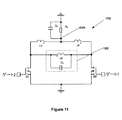
更なる実施形態において、図11に示される受信回路1000が提供され、受信回路1000は、共振タンク1002を形成するためにチューニングコンデンサC3と並列に接続された単一の(ループ)コイルL5を備える。2つの(分割された)DCインダクタL4,L8は、共振タンク1002を、平滑コンデンサC2と並列に示されている受電器3の(DC)負荷R9(11)に接続されたDC電圧出力ノード1004に接続している。図8と同様に、2つのスイッチQ1,Q2は、プッシュプル構成又は倍電流整流構成で、共振タンク1002に接続され、同様に操作される。
In a further embodiment, a
図10の回路は、例えば、送信コイルと受信コイルとの間に一定の結合係数が存在する状況において、又は回路のサイズ及び複雑度が、出力電圧のリップルより優先される場合に、図11の回路よりも有益である。これは、図11の回路が多くのDCインダクタを含むためである。これらのインダクタは、システムに対して安定性をもたらすとともに、DC出力のリップルがこの構成によって低くなるように、DC出力電流を平滑化する役割を果たすが、図10の実施形態と比べて回路サイズが大きくなる。また、従来の単一インダクタの受信コイルが利用されうることで、受信機の製造がより単純に、かつ、より安くなりうる。 The circuit of FIG. 10 is, for example, in a situation where there is a constant coupling coefficient between the transmitter coil and the receiver coil, or when the size and complexity of the circuit takes precedence over the ripple of the output voltage. It is more beneficial than a circuit. This is because the circuit of FIG. 11 includes many DC inductors. These inductors provide stability to the system and serve to smooth the DC output current so that the DC output ripple is reduced by this configuration, but the circuit size compared to the embodiment of FIG. Becomes larger. Also, since a conventional single inductor receiving coil can be used, the manufacture of the receiver can be simpler and cheaper.
発明の実施形態の記述によって本発明を説明してきたが、また、実施形態を詳細に説明してきたが、添付の請求項の範囲を多少なりともそのような詳細に限定することは、出願人の意図ではない。更なる利点及び変更が、当業者には容易に見てとれることになる。したがって、より広い態様の発明が、図示及び記述されている具体的な詳細、代表的な装置及び方法、並びに例示的な例に限定されることはない。このため、出願人の全体的な発明概念の精神または範囲から逸脱することなく、そのような詳細からの逸脱がなされてもよい。 While the invention has been described in terms of the description of the embodiments of the invention, and the embodiments have been described in detail, it is the applicant's intention to limit the scope of the appended claims in any way to such details. Not intended. Additional advantages and modifications will be readily apparent to those skilled in the art. Accordingly, the broader aspects of the invention are not limited to the specific details, representative apparatus and methods, and illustrative examples shown and described. Accordingly, departures may be made from such details without departing from the spirit or scope of applicants' general inventive concept.
Claims (12)
前記少なくとも2つのスイッチのうちの第1スイッチは、受電器変数に依存した第1イベントに基づいて第1状態に切り替わるように構成され、
前記第1スイッチは、受電器変数に依存しない第2イベントに基づいて第2状態に切り替わるように構成されている、受電器。 An inductive power receiver comprising at least two switches connected via a resonant circuit, the resonant circuit including an inductance and a capacitance;
A first switch of the at least two switches is configured to switch to a first state based on a first event dependent on a receiver variable;
The first switch is configured to switch to a second state based on a second event that does not depend on a receiver variable.
整流回路である、受電器。 The power receiver according to claim 1, wherein the combination of the at least two switches connected via a resonant circuit is a modified push-pull converter or a modified current doubler rectifier circuit. .
Applications Claiming Priority (3)
| Application Number | Priority Date | Filing Date | Title |
|---|---|---|---|
| US201462067108P | 2014-10-22 | 2014-10-22 | |
| US62/067,108 | 2014-10-22 | ||
| PCT/NZ2015/050175 WO2016064283A1 (en) | 2014-10-22 | 2015-10-21 | A converter |
Publications (2)
| Publication Number | Publication Date |
|---|---|
| JP2017537588A true JP2017537588A (en) | 2017-12-14 |
| JP2017537588A5 JP2017537588A5 (en) | 2018-11-29 |
Family
ID=55761211
Family Applications (1)
| Application Number | Title | Priority Date | Filing Date |
|---|---|---|---|
| JP2017522037A Pending JP2017537588A (en) | 2014-10-22 | 2015-10-21 | converter |
Country Status (6)
| Country | Link |
|---|---|
| US (1) | US20170358954A1 (en) |
| EP (1) | EP3210294A4 (en) |
| JP (1) | JP2017537588A (en) |
| KR (1) | KR20170071604A (en) |
| CN (1) | CN107078651A (en) |
| WO (1) | WO2016064283A1 (en) |
Families Citing this family (10)
| Publication number | Priority date | Publication date | Assignee | Title |
|---|---|---|---|---|
| CN105765839B (en) * | 2013-09-12 | 2018-10-12 | 奥克兰联合服务有限公司 | Resonant power with self-tuning |
| WO2016072865A1 (en) * | 2014-11-05 | 2016-05-12 | Powerbyproxi Limited | An inductive power receiver |
| US10333335B2 (en) * | 2017-10-27 | 2019-06-25 | Lear Corporation | System and method of electric vehicle wireless charger output protection using zero voltage switching |
| CN113454875A (en) * | 2019-02-08 | 2021-09-28 | 奥克兰大学服务有限公司 | Inductive power transfer coupler array |
| CN109888863A (en) * | 2019-02-22 | 2019-06-14 | 苏州加士革电子科技有限公司 | A kind of wireless power transmission system for charging the battery |
| BR102020006101A2 (en) | 2019-04-17 | 2020-11-03 | Mettler-Toledo Safeline Limited | METHOD FOR OPERATING A METAL DETECTOR AND METAL DETECTOR |
| BR102020006536A2 (en) | 2019-04-17 | 2020-10-27 | Mettler-Toledo Safeline Ltd. | method for operating a metal detector and metal detector |
| EP3726255A1 (en) | 2019-04-17 | 2020-10-21 | Mettler-Toledo Safeline Limited | Method for operating a metal detector and metal detector |
| US11770017B2 (en) | 2019-10-24 | 2023-09-26 | Medtronic, Inc. | Self tuning class D driver for maximum power factor in wireless recharger |
| CN116979711B (en) * | 2023-03-10 | 2024-04-23 | 巨翼(苏州)新动力有限公司 | Magnetic induction wireless charging receiver combining double rectification and energy flow control |
Citations (4)
| Publication number | Priority date | Publication date | Assignee | Title |
|---|---|---|---|---|
| WO2012035745A1 (en) * | 2010-09-16 | 2012-03-22 | 株式会社アドバンテスト | Wireless energy transfer device and wireless energy transfer system |
| JP2012139011A (en) * | 2010-12-27 | 2012-07-19 | Contec Co Ltd | Secondary power reception circuit of non-contact power supply facility |
| WO2014042681A2 (en) * | 2012-09-11 | 2014-03-20 | Access Business Group International Llc | Wireless power control |
| JP2014082897A (en) * | 2012-10-18 | 2014-05-08 | Advantest Corp | Wireless power-receiving device, impedance control circuit available for the same, and impedance control method |
Family Cites Families (7)
| Publication number | Priority date | Publication date | Assignee | Title |
|---|---|---|---|---|
| JP2803943B2 (en) * | 1992-10-21 | 1998-09-24 | アルプス電気株式会社 | Non-contact power supply |
| CN101728965B (en) * | 2008-10-21 | 2012-01-25 | 全汉企业股份有限公司 | Resonance oscillation converter for improving synchronous rectification control |
| NZ593946A (en) * | 2011-07-07 | 2014-05-30 | Powerbyproxi Ltd | An inductively coupled power transfer receiver |
| EP2777142A4 (en) * | 2011-11-10 | 2016-07-27 | Powerbyproxi Ltd | A method for controlling a converter |
| JP2013115932A (en) * | 2011-11-29 | 2013-06-10 | Ihi Corp | Non-contact power transmission apparatus and method |
| WO2015156689A1 (en) * | 2014-04-09 | 2015-10-15 | Auckland Uniservices Limited | Inductive power transfer converters and system |
| CN104079079B (en) * | 2014-07-14 | 2018-02-23 | 南京矽力杰半导体技术有限公司 | Mode of resonance contactless power supply device, integrated circuit and constant pressure control method |
-
2015
- 2015-10-21 JP JP2017522037A patent/JP2017537588A/en active Pending
- 2015-10-21 KR KR1020177013819A patent/KR20170071604A/en unknown
- 2015-10-21 WO PCT/NZ2015/050175 patent/WO2016064283A1/en active Application Filing
- 2015-10-21 EP EP15853474.3A patent/EP3210294A4/en not_active Withdrawn
- 2015-10-21 CN CN201580057711.5A patent/CN107078651A/en active Pending
- 2015-10-21 US US15/521,084 patent/US20170358954A1/en not_active Abandoned
Patent Citations (4)
| Publication number | Priority date | Publication date | Assignee | Title |
|---|---|---|---|---|
| WO2012035745A1 (en) * | 2010-09-16 | 2012-03-22 | 株式会社アドバンテスト | Wireless energy transfer device and wireless energy transfer system |
| JP2012139011A (en) * | 2010-12-27 | 2012-07-19 | Contec Co Ltd | Secondary power reception circuit of non-contact power supply facility |
| WO2014042681A2 (en) * | 2012-09-11 | 2014-03-20 | Access Business Group International Llc | Wireless power control |
| JP2014082897A (en) * | 2012-10-18 | 2014-05-08 | Advantest Corp | Wireless power-receiving device, impedance control circuit available for the same, and impedance control method |
Also Published As
| Publication number | Publication date |
|---|---|
| EP3210294A1 (en) | 2017-08-30 |
| EP3210294A4 (en) | 2017-11-15 |
| CN107078651A (en) | 2017-08-18 |
| KR20170071604A (en) | 2017-06-23 |
| US20170358954A1 (en) | 2017-12-14 |
| WO2016064283A1 (en) | 2016-04-28 |
Similar Documents
| Publication | Publication Date | Title |
|---|---|---|
| JP2017537588A (en) | converter | |
| US10923953B2 (en) | Received wireless power regulation | |
| US10038389B2 (en) | Method for controlling a converter | |
| JP6103061B2 (en) | Power feeding device and non-contact power feeding system | |
| KR102139841B1 (en) | A receiver for an inductive power transfer system and a method for controlling the receiver | |
| TWI689165B (en) | On and off controlled resonant dc-dc power converter and operating method | |
| KR101405878B1 (en) | Power transmission system | |
| US20150364947A1 (en) | Power-supplying device, and wireless power-supplying system | |
| JP2015002668A (en) | Power-supply device | |
| US10447090B1 (en) | Inductive power receiver | |
| JP2017539194A (en) | Induction power receiver | |
| JP2016092959A (en) | Power transmission equipment and contactless power transmission device | |
| JP7356102B2 (en) | Wireless power supply device | |
| WO2017105256A1 (en) | Inductive power receiver | |
| JP2018509876A (en) | Inductive power receiver | |
| US20180034324A1 (en) | Inductive power receiver | |
| WO2020116033A1 (en) | Non-contact power feeding device |
Legal Events
| Date | Code | Title | Description |
|---|---|---|---|
| A711 | Notification of change in applicant |
Free format text: JAPANESE INTERMEDIATE CODE: A711 Effective date: 20180227 |
|
| A521 | Request for written amendment filed |
Free format text: JAPANESE INTERMEDIATE CODE: A523 Effective date: 20181016 |
|
| A621 | Written request for application examination |
Free format text: JAPANESE INTERMEDIATE CODE: A621 Effective date: 20181016 |
|
| A977 | Report on retrieval |
Free format text: JAPANESE INTERMEDIATE CODE: A971007 Effective date: 20191028 |
|
| A131 | Notification of reasons for refusal |
Free format text: JAPANESE INTERMEDIATE CODE: A131 Effective date: 20191125 |
|
| A521 | Request for written amendment filed |
Free format text: JAPANESE INTERMEDIATE CODE: A523 Effective date: 20200221 |
|
| A131 | Notification of reasons for refusal |
Free format text: JAPANESE INTERMEDIATE CODE: A131 Effective date: 20200323 |
|
| A02 | Decision of refusal |
Free format text: JAPANESE INTERMEDIATE CODE: A02 Effective date: 20201012 |