JP2017123703A - Dc-dc converter - Google Patents
Dc-dc converter Download PDFInfo
- Publication number
- JP2017123703A JP2017123703A JP2016000332A JP2016000332A JP2017123703A JP 2017123703 A JP2017123703 A JP 2017123703A JP 2016000332 A JP2016000332 A JP 2016000332A JP 2016000332 A JP2016000332 A JP 2016000332A JP 2017123703 A JP2017123703 A JP 2017123703A
- Authority
- JP
- Japan
- Prior art keywords
- voltage
- switching circuit
- voltage side
- low
- side switching
- Prior art date
- Legal status (The legal status is an assumption and is not a legal conclusion. Google has not performed a legal analysis and makes no representation as to the accuracy of the status listed.)
- Pending
Links
Images


Abstract
Description
本発明は、DCDCコンバータに関する。 The present invention relates to a DCDC converter.
DCDCコンバータは、運転停止時等に、高電圧入力側に接続された高電圧バッテリから切り離される。このとき、DCDCコンバータは、高電圧入力側のコンデンサに充電された電圧を、抵抗を使用して安全電圧まで放電している。 The DCDC converter is disconnected from the high voltage battery connected to the high voltage input side when the operation is stopped. At this time, the DCDC converter discharges the voltage charged in the capacitor on the high voltage input side to a safe voltage using a resistor.
しかしながら、抵抗による放電は、電力を熱として無駄に消費するものである。
本発明は、上記の点に鑑みてなされたものであり、その目的とするところは、高電圧入力側のコンデンサに残存するエネルギーを、低電圧バッテリに回収して電力の浪費を防ぐことができるDCDCコンバータを提供することである。
However, discharge by resistance consumes power wastefully as heat.
The present invention has been made in view of the above points, and an object of the present invention is to recover the energy remaining in the capacitor on the high voltage input side to the low voltage battery and prevent waste of power. It is to provide a DCDC converter.
上記課題を解決する本発明のDCDCコンバータは、高電圧電源と接続される高電圧側スイッチング回路と、低電圧電源と接続される低電圧側スイッチング回路と、前記高電圧側スイッチング回路と前記低電圧側スイッチング回路を磁気的に接続するトランスと、前記高電圧側スイッチング回路に電気的に並列に接続されたコンデンサとを備え、前記低電圧側スイッチング回路は、前記コンデンサの電荷を前記トランスを介して前記低電圧電源に放電することを特徴とする。 The DCDC converter of the present invention that solves the above problems includes a high voltage side switching circuit connected to a high voltage power supply, a low voltage side switching circuit connected to a low voltage power supply, the high voltage side switching circuit, and the low voltage A transformer that magnetically connects the side switching circuit, and a capacitor that is electrically connected in parallel to the high-voltage side switching circuit, and the low-voltage side switching circuit passes the charge of the capacitor through the transformer The low-voltage power supply is discharged.
本発明によれば、高電圧バッテリから切り離したときに高電圧入力側のコンデンサに残存するエネルギーを、低電圧バッテリに回収して電力の浪費を防ぐことができる。なお、上記した以外の課題、構成及び効果は、以下の実施形態の説明により明らかにされる。 According to the present invention, energy remaining in the capacitor on the high voltage input side when disconnected from the high voltage battery can be recovered in the low voltage battery to prevent waste of electric power. Problems, configurations, and effects other than those described above will be clarified by the following description of the embodiments.
次に、本発明の対象となるDCDCコンバータとその周辺構成および動作概要について図面を用いて説明する。 Next, a DCDC converter which is a subject of the present invention, its peripheral configuration and an outline of operation will be described with reference to the drawings.
[実施例1]
図1は、実施例1におけるDCDCコンバータとその周辺の構成を説明する図である。
DCDCコンバータ102は、入力側に高電圧バッテリ100が接続され、出力側に低電圧バッテリ104と低電圧側負荷105が接続されている。DCDCコンバータ102は、高電圧バッテリ100から供給された高電圧を低電圧に変換し、低電圧バッテリ104や低電圧側負荷105に電力を供給する。
[Example 1]
FIG. 1 is a diagram for explaining a DCDC converter and its peripheral configuration in the first embodiment.
The
低電圧バッテリ104は、電力貯蔵媒体であり、DCDCコンバータ102から電力の供給を受け、低電圧側負荷105へ電力を供給する。低電圧側負荷105は、DCDCコンバータ102や、低電圧バッテリ104より電力の供給を受けて動作する負荷装置である。
The
高電圧バッテリ100は、電力貯蔵媒体であり、DCDCコンバータ102の電力源となる。高電圧バッテリ100とDCDCコンバータ102は、車両ECU103によって制御される。車両ECU103は、電動車両の動作を制御するユニットであり、高電圧リレー101とDCDCコンバータ102に動作指令を送る。高電圧リレー101は、高電圧バッテリ100とDCDCコンバータ102との間に配置されており、車両ECU103からの制御信号に基づいて高電圧バッテリ100とDCDCコンバータ102との間の電力の流れを遮断する。
The
DCDCコンバータ102は、DCDC制御装置106と、高電圧側スイッチング回路107と、低電圧側スイッチング回路108を有している。DCDC制御装置106は、車載ECU103から指令を受け、高電圧側スイッチング回路107と、低電圧側スイッチング回路108に駆動信号を与えて、DCDCコンバータ102の出力を制御する。
The
高電圧側スイッチング回路107は、Leg1とLeg2を有している。Leg1は、MOSFET_Q1とMOSFET_Q2で構成され、MOSFET_Q1とMOSFET_Q2のON・OFF状態は反転した関係になる。同様にLeg2は、MOSFET_Q3とMOSFET_Q4で構成され、MOSFET_Q3とMOSFET_Q4のON・OFF状態は反転した関係になる。
The high voltage
Leg1に対するLeg2の位相を制御し、出力電圧Voutの制御を行う。具体的には、位相を制御することにより、MOSFET_Q1とMOSFET_Q3、MOSFET_Q2とMOSFET_Q4が同時にONとなる期間を長くすることで出力を上げ、短くすることで出力を下げる。DCDC制御装置106より、スイッチング素子であるMOSFET_Q1〜Q4に与えられるON・OFF駆動信号は全て固定周波数でON+OFFに対するONの比率が約50%である。
The phase of Leg2 with respect to Leg1 is controlled to control the output voltage Vout. Specifically, by controlling the phase, the output is increased by increasing the period in which MOSFET_Q1 and MOSFET_Q3, MOSFET_Q2 and MOSFET_Q4 are simultaneously ON, and the output is decreased by shortening. The ON / OFF drive signals given from the
高電圧側スイッチング回路107よりも高電圧側には、放電回路109と、高電圧側コンデンサC1が配置されている。放電回路109は、高電圧側コンデンサC1の電圧を放電する回路であり、抵抗R1とリレーRL1から構成される。高電圧側コンデンサC1は、DCDCコンバータ102内の高電圧入力側に配置され、電圧変動を抑制する。
On the higher voltage side than the high voltage
高電圧側スイッチング回路107と低電圧側スイッチング回路108との間には、リアクトルL1と絶縁トランスT1が配置されている。リアクトルL1は、共振リアクトルで高電圧側スイッチング回路107のQ1〜Q4がスイッチングする際、共振電流を流し、スイッチング時の損失を低減する。絶縁トランスT1は、入力された一次側の電圧を絶縁した電圧に変換し、二次側に出力する。
Between the high voltage
低電圧側スイッチング回路108よりも低電圧側には、リアクトルL2と、スイッチ110と、低電圧側コンデンサC2が配置されている。リアクトルL2と低電圧側コンデンサC2は、低電圧側スイッチング回路108が出力する、整流された矩形波電圧の平滑を行う。スイッチ110は、リアクトルL2を短絡するスイッチであり、半導体スイッチもしくは、リレーのような機械的スイッチである。
A reactor L2, a
電圧検出器VT1は、高電圧側スイッチング回路107よりも高電圧側に配置され、電圧検出器VT2と電流検出器CT1は、低電圧側スイッチング回路108よりも低電圧側に配置されている。電圧検出器VT1は、DCDCコンバータ102の入力電圧の検出を行う。電圧検出器VT2は、DCDCコンバータ102の出力電圧の検出を行う。電流検出器CT1は、DCDCコンバータ102の出力電流の検出を行う。
The voltage detector VT1 is arranged on the higher voltage side than the high voltage
DCDC制御装置106は、高電圧側スイッチング回路107のMOSFET_Q1〜Q4をスイッチングし、高電圧バッテリ100から供給された電圧を交流矩形波電圧に変換し、共振リアクトルL1と絶縁トランスT1の一次側に出力させる。そして、絶縁トランスT1の二次側から交流矩形波電圧を受電させ、低電圧側スイッチング回路108のMOSFET_Q5〜Q8をスイッチングし、低損失に交流矩形波電圧の整流を行う。
The
ダイオードD5〜D8と比較して、MOSFET_Q5〜Q8の導通損失は小さいため、ダイオードD5〜D8に電流が流れるタイミングでMOSFET_Q5〜Q8をONすることで導通損失を低減している。具体的には、MOSFET_Q1とMOSFET_Q3が同時にONする期間はMOSFET_Q5とMOSFET_Q7をONし、MOSFET_Q2とMOSFET_Q4が同時にONする期間はMOSFET_Q6とMOSFET_Q8をONし、交流矩形波電圧の整流を行う。低電圧側スイッチング回路108から出力された、整流された矩形波電圧はリアクトルL2とコンデンサC2にて直流平滑化され、低電圧バッテリ104と低電圧側負荷105に電力供給される。
Since the conduction losses of MOSFET_Q5 to Q8 are small compared to the diodes D5 to D8, the conduction losses are reduced by turning on the MOSFET_Q5 to Q8 at the timing when the current flows through the diodes D5 to D8. Specifically, MOSFET_Q5 and MOSFET_Q7 are turned on during the period in which MOSFET_Q1 and MOSFET_Q3 are simultaneously turned on, and MOSFET_Q6 and MOSFET_Q8 are turned on during the period in which MOSFET_Q2 and MOSFET_Q4 are simultaneously turned on to rectify the AC rectangular wave voltage. The rectified rectangular wave voltage output from the low voltage
DCDCコンバータ102が運転を停止する際は、まず、車両ECU103からDCDCコンバータ102へ運転停止指令が送られ、高電圧側スイッチング回路107のMOSFET_Q1〜Q4及び低電圧側スイッチング回路108のMOSFET_Q5〜Q8のスイッチングを停止する。そして、車両ECU103からリレー遮断指令が送られ、高電圧リレー101がOFF状態とされる。
When the DCDC converter 102 stops operation, first, an operation stop command is sent from the
DCDCコンバータ102の高電圧側スイッチング回路107のMOSFET_Q1〜Q4及び低電圧側スイッチング回路108のMOSFET_Q5〜Q8は、高電圧リレー101がOFF状態とされる前にスイッチングを停止しているため、高電圧側コンデンサC1の電圧は放電されず、高電圧バッテリ100と同等の電圧に維持される。
The MOSFET_Q1 to Q4 of the high voltage
高電圧側コンデンサC1が高電圧を維持することは、保守員が保守作業時に高電圧側コンデンサC1に接触し感電する等、安全面で問題がある。よって、高電圧側コンデンサC1の電荷を放電して電圧を安全電圧まで低下させる必要がある。 The fact that the high voltage side capacitor C1 maintains a high voltage has a problem in terms of safety, for example, maintenance personnel come into contact with the high voltage side capacitor C1 during maintenance work and receive an electric shock. Therefore, it is necessary to discharge the charge of the high voltage side capacitor C1 to reduce the voltage to a safe voltage.
従来の高電圧側コンデンサC1の電圧を放電する方法として、放電回路109のリレーRL1をON状態にして、高電圧側コンデンサC1に対して抵抗R1を並列に接続した状態としていた。したがって、高電圧側コンデンサC1の電圧は、抵抗R1による電力消費により放電されていた。しかし、抵抗での電力消費による放電は、電力を熱として無駄に消費するという課題があった。
As a conventional method of discharging the voltage of the high voltage side capacitor C1, the relay RL1 of the
本実施例のDCDCコンバータ102は、上記課題に鑑みてなされたものであり、高電圧側コンデンサC1の電圧を、高電圧側スイッチング回路107で交流矩形波電圧に変換し、絶縁トランスT1で絶縁を行い、低電圧側スイッチング回路108で整流を行い、リアクトルL2、コンデンサC2で平滑を行うことで低電圧に変換し、低電圧バッテリ104に電力を供給することで、高電圧側コンデンサC1の電圧の放電を行う、つまり、高電圧側コンデンサC1に残存するエネルギーを低電圧バッテリ104で回収することで電力の浪費を防いでいる。
The
次に、高電圧側コンデンサC1の電圧を低電圧バッテリ104に電力供給する方法について説明する。
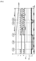
図2は、実施例1におけるDCDCコンバータの動作状態と高電圧側コンデンサの電圧の変化を示すタイミング図である。図2の縦軸の一番上のチャートは、高電圧側コンデンサC1の電圧VINの変化を示すものである。図2に示す比率DHは、高電圧側スイッチング回路107のMOSFET_Q1〜Q4がスイッチングする周期に対してQ1とQ3およびQ2とQ4が同時にONする期間の比率であり、比率DLは、低電圧側スイッチング回路108のMOSFET_Q5〜Q8がスイッチングする周期に対するQ5とQ7およびQ6とQ8が同時にONする期間の比率である。高電圧リレー駆動信号SIGHVRLYは、車両ECU103により高電圧リレー101を駆動する信号であり、出力電圧VOUTは、DCDCコンバータ102の出力電圧、電圧VLVBは、低電圧バッテリ104の電圧である。
Next, a method of supplying the voltage of the high voltage side capacitor C1 to the
FIG. 2 is a timing chart showing changes in the operating state of the DCDC converter and the voltage of the high voltage side capacitor in the first embodiment. The top chart on the vertical axis in FIG. 2 shows the change in the voltage VIN of the high voltage side capacitor C1. Ratio D H shown in FIG. 2, Q1 and Q3 and Q2 and Q4 relative period MOSFET_Q1~Q4 is switched on the high voltage
図2の期間1では、高電圧バッテリ100の電圧を、高電圧側スイッチング回路107で交流矩形波電圧に変換し、絶縁トランスT1で絶縁を行い、低電圧側スイッチング回路108で整流を行い、リアクトルL2、コンデンサC2で平滑を行うことで低電圧に変換を行い、低電圧バッテリ104に電力を供給している。そして、A点でDCDCコンバータ102に対して車両ECU103から運転停止指令が送られると、これを受けたDCDCコンバータ102は、高電圧側スイッチング回路107と低電圧側スイッチング回路108に対する駆動信号の出力を停止する。期間2では、高電圧側スイッチング回路107及び、低電圧側スイッチング回路108は、スイッチングを停止しているが、高電圧リレー101はON状態となっている。
In period 1 of FIG. 2, the voltage of the
次に、B点にて、車両ECU103からのリレー遮断指令により高電圧リレー101はOFF状態となる。したがって、期間3では、高電圧側コンデンサC1は放電されず、概ね高電圧バッテリ100の電圧を維持している。
Next, at point B, the
そして、C点にて、高電圧側スイッチング回路107、低電圧側スイッチング回路108のスイッチングが開始される。期間4では、スイッチングにより、高電圧側コンデンサC1の電圧が高電圧側スイッチング回路107で交流矩形波電圧に変換される。そして、絶縁トランスT1で絶縁を行い、低電圧側スイッチング回路108で整流を行い、リアクトルL2、低電圧側コンデンサC2で平滑を行うことで低電圧に変換される。そして、低電圧バッテリ104に電力の供給を行うことで高電圧側コンデンサC1の電圧の放電を行う。
Then, at the point C, switching of the high voltage
高電圧側コンデンサC1の電圧は、低電圧バッテリ104に電力供給を行うことで低下する。高電圧側コンデンサC1の電圧低下に対して、低電圧バッテリ104への電力供給を継続するためには、DCDCコンバータ102の出力電圧Voutを低電圧側バッテリ104へ電力を供給可能な高い電圧に維持する必要がある。すなわち、DCDCコンバータ102が低電圧バッテリ104に電力を供給するためには、DCDCコンバータ102の出力電圧Voutを、低電圧バッテリ104に電力を供給できる電圧、つまり低電圧バッテリ104の電圧VLVBより高い値に制御する必要がある。
The voltage of the high voltage side capacitor C <b> 1 decreases by supplying power to the
高電圧側コンデンサC1の電圧Vinと、高電圧側スイッチング回路107のMOSFET_Q1〜Q4がスイッチングする周期に対してQ1とQ3およびQ2とQ4が同時にONする期間の比率DH(デューティー比)と、絶縁トランスT1の一次側と二次側の巻き数比Nと、DCDCコンバータの出力電圧Voutには以下(1)式の関係がある。
The voltage Vin of the high-voltage side capacitor C1, the ratio DH (duty ratio) of the period in which Q1 and Q3 and Q2 and Q4 are simultaneously turned on with respect to the period of switching of the MOSFET_Q1 to Q4 of the high-voltage
![]()
![]()
高電圧側コンデンサC1の電圧VINの放電による低下(減少)に伴い、高電圧側スイッチング回路107のMOSFET_Q1〜Q4がスイッチングする周期に対してQ1とQ3が同時にONする期間の比率DHを大きくし(増加させ)、出力電圧Voutを低電圧バッテリ104に電力供給可能な電圧に制御を行う。また、低電圧側スイッチング回路108のMOSFET_Q5〜Q8がスイッチングする周期に対するQ5とQ7が同時にONする期間の比率DLは、低電圧側スイッチング回路108の導通損失低減のため比率DHに同期させる。
As the voltage VIN of the high voltage side capacitor C1 decreases (decreases) due to the discharge, the ratio DH of the period in which Q1 and Q3 are simultaneously turned on increases with respect to the switching period of the MOSFET_Q1 to Q4 of the high voltage
つまり、絶縁トランスT1の巻き数比Nが固定であるのに対して高電圧側コンデンサC1の電圧VINが低下するが、(1)式よりVoutを一定に保つために、高電圧側スイッチング回路107のMOSFET_Q1〜Q4がスイッチングする周期に対するQ1とQ3およびQ2とQ4が同時にONする期間の比率DHを電圧Vinの低下(減少)に伴い大きくして(増加させて)、出力電圧Voutを低電圧バッテリ104に電力供給な電圧に制御している(第1モード)。
That is, the voltage VIN of the high-voltage side capacitor C1 is lowered while the turn ratio N of the insulating transformer T1 is fixed. However, in order to keep Vout constant from the equation (1), the high-voltage
このとき、低電圧側スイッチング回路108のON期間は、高電圧側スイッチング回路107のMOSFET_Q1〜Q4がスイッチングする周期に対するQ1とQ3およびQ2とQ4が同時にONする期間の比率DHと同期させることで、低電圧側スイッチング回路108の導通損失を低減し、より多くの電力を低電圧バッテリ104に回収することができる。
At this time, the ON period of the low voltage
なお、D点にて、高電圧側スイッチング回路107のMOSFET_Q1〜Q4がスイッチングする周期に対してQ1とQ3が同時にONする期間の比率DHは最大値で飽和する。したがって、期間5では、低電圧側スイッチング回路108のMOSFET_Q5〜Q8がスイッチングする周期に対するQ5とQ7が同時にONする期間の比率DLも同様に最大値で飽和しており、出力電圧Voutを低電圧バッテリ104に電力を供給可能な高い電圧に制御することができず、高電圧側コンデンサC1の電圧の低下が進まない状態となる。かかる状態で、例えば放電回路109のリレーRL1を接続して、抵抗R1による電力消費により高電圧側コンデンサC1の電圧VINを安全電圧まで低下させることもできる。
At the point D, the ratio DH of the period in which Q1 and Q3 are simultaneously turned on with respect to the period of switching of the MOSFET_Q1 to Q4 of the high voltage
[実施例2]
次に、本発明の実施例2について図3から図5を用いて説明する。
本実施例において特徴的なことは、期間5のあとに、低電圧側スイッチング回路108を、昇圧型コンバータとして動作する第2モードに切り替えて、高電圧側コンデンサC1の電圧VINを安全電圧まで放電させることである。
[Example 2]
Next, a second embodiment of the present invention will be described with reference to FIGS.
What is characteristic in this embodiment is that, after period 5, the low-voltage
実施例1の期間4では、高電圧側コンデンサC1の電圧低下に伴い比率DHを大きくしていくが、比率DHが最大値のD点に達すると、(1)式より絶縁トランスT1の巻数比Nと高電圧側スイッチング回路107のMOSFET_Q1〜Q4がスイッチングする周期に対するQ1とQ3およびQ2とQ4が同時にONする期間の比率DHが最大で飽和して固定値になる。したがって、期間5では、高電圧側コンデンサC1の電圧VINの低下に比例してDCDCコンバータ102の出力電圧Voutは低下し、低電圧バッテリ104に対して電力供給が可能な高い電圧に制御することができず、高電圧側コンデンサC1の電圧を放電することができない状態となる。
In the
本実施例では、高電圧スイッチング回路107のMOSFET_Q1〜Q4のスイッチング周期に対するQ1とQ3およびQ2とQ4が同時にONする期間の比率DHが最大値に達した状態から、さらにDCDCコンバータ102の出力電圧Voutを低電圧バッテリ104に電力を供給可能な高い電圧に制御するために、DCDCコンバータ102を昇圧型コンバータとして動作させる制御を行う。
In this embodiment, a state where the ratio D H period Q1 and Q3 and Q2 and Q4 to the switching period of MOSFET_Q1~Q4 high
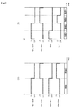
図3は、実施例2におけるDCDCコンバータの動作状態と高電圧側コンデンサの電圧の変化を示すタイミング図である。 FIG. 3 is a timing chart showing changes in the operating state of the DCDC converter and the voltage of the high voltage side capacitor in the second embodiment.
実施例1では、D点にて高電圧側スイッチング回路107のMOSFET_Q1〜Q4がスイッチングする周期に対してQ1とQ3およびQ2とQ4が同時にONする期間の比率DHが最大で飽和すると、期間5ではDCDCコンバータ102は出力電圧Voutを、低電圧バッテリ104に対して電力供給が可能な高い電圧に制御を行うことができず、高電圧側コンデンサC1の電圧の放電を行うことができない状態となる。
In Example 1, the ratio D H period Q1 and Q3 and Q2 and Q4 relative period MOSFET_Q1~Q4 is switched on the high voltage
本実施例では、期間5において、高電圧側スイッチング回路107のMOSFET_Q1〜Q4がスイッチングする周期に対してQ1とQ3およびQ2とQ4が同時にONする期間の比率DHの飽和と、高電圧側コンデンサC1の電圧の低下率の低下を検知すると(図3のE点)、低電圧側スイッチング回路108が高電圧側スイッチング回路107に同期していた第1モードから、低電圧側スイッチング回路108が昇圧型コンバータとして動作する第2モードに切り替える。
In the present embodiment, in period 5, the saturation of ratio DH of the period in which Q1 and Q3 and Q2 and Q4 are simultaneously turned on with respect to the period of switching of MOSFET_Q1 to Q4 of high voltage
期間6の第2モードでは、昇圧型コンバータとしては不要となるリアクトルL2を、スイッチ110をONすることで短絡させ、高電圧側スイッチング回路107のMOSFET_Q1〜Q4は、スイッチングする周期に対するQ1とQ3およびQ2とQ4が同時にONする期間の比率DHを最大値で固定し、低電圧側スイッチング回路108を昇圧コンバータとして動作させる。これにより、出力電圧Voutを低電圧バッテリ104に電力を供給可能な高い電圧に制御し、高電圧側コンデンサC1の電圧の放電を行う。
In the second mode of period 6, the reactor L2, which is not necessary as a step-up converter, is short-circuited by turning on the
次に、第2モードについて詳細に説明する。
まずは、図1を用いて第2モードの回路方式の説明を行う。第2モードでは、DCDCコンバータ102を昇圧型コンバータとして動作させるために、リアクトルL1を昇圧用リアクトルとして使用し、MOSFET_Q6,Q7を昇圧用スイッチング素子として使用する。そして、ダイオードD5〜D8を昇圧用整流素子として使用し、コンデンサC2を平滑コンデンサとして使用する。低電圧側スイッチング回路108は、低電圧側スイッチング回路108に印可される電圧を昇圧させて低電圧バッテリ104の電圧よりも大きくする。
Next, the second mode will be described in detail.
First, the second mode circuit system will be described with reference to FIG. In the second mode, in order to operate the
一方、リアクトルL2は、第1モードでは、降圧型コンバータの平滑リアクトルとして使用していたが、昇圧型コンバータとして動作させるときには、低電圧側スイッチング回路107のMOSFET_Q5〜Q8を過電圧にて破損させる可能性があるため、スイッチ110を使用して、短絡状態とする。過電圧になる原因は、リアクトルL2を流れる電流は、MOSFET_Q6、Q7が昇圧動作としてON、OFFする際、ONしている期間にリアクトル電流を流す経路が無くなり、電流が連続にならず電流変化が急峻となるからである。
On the other hand, reactor L2 was used as a smoothing reactor for the step-down converter in the first mode, but when operated as a step-up converter, MOSFET_Q5 to Q8 of low voltage
リアクトルL2のL値は固定値であるため、(2)式よりリアクトルL2の電流変化率が大きくなると電圧VLは大きくなり過電圧の原因となる。 Since the L value of the reactor L2 is a fixed value, the voltage V L increases as the current change rate of the reactor L2 increases from the equation (2), causing overvoltage.

本実施例におけるMOSFET_Q1〜Q8の動作について図4、図5を用いて説明を行う。 The operation of MOSFET_Q1 to Q8 in this embodiment will be described with reference to FIGS.
図4(a)は、比率DHにて出力電圧の制御を行い、低電圧側スイッチング回路108のMOSFET_Q5〜Q8が整流動作時の導通損失を低減するために、高電圧側スイッチング回路107のQ1〜Q4に同期した第1モードにおいて、比率DHが最大の状態のQ1〜Q8の駆動信号を示している。
FIG. 4A shows the control of the output voltage at the ratio DH , and the MOSFET_Q5 to Q8 of the low voltage
図4(a)に示す期間1では、MOSFET_Q1、Q3がONし、Q2、Q4がOFFし、リアクトルL1、絶縁トランスT1に電流を流し、絶縁トランスT1の二次側に正の電圧を出力する。このとき、MOSFET_Q5、Q7をONし、Q6、Q8をOFFし、整流を行い、低電圧バッテリ104に電力供給を行う。
In period 1 shown in FIG. 4A, MOSFET_Q1 and Q3 are turned on, Q2 and Q4 are turned off, current flows through reactor L1 and insulation transformer T1, and a positive voltage is output to the secondary side of insulation transformer T1. . At this time, MOSFET_Q5 and Q7 are turned on, Q6 and Q8 are turned off, rectification is performed, and power is supplied to the
そして、期間2では、MOSFET_Q1、Q3がOFFし、Q2、Q4がONし、リアクトルL1、絶縁トランスT1に電流を流し、絶縁トランスT1の二次側に負の電圧を出力する。このとき、MOSFET_Q5、Q7をOFFし、Q6、Q8をONし、整流を行い、低電圧バッテリ104に電力供給を行う。
In
図4(b)は、比率DHが最大かつ、低電圧側スイッチング回路108のMOSFET_Q5〜Q8が昇圧動作を行っている第2モードのQ1〜Q8の駆動信号を示している。
FIG. 4B shows the driving signals of Q1 to Q8 in the second mode in which the ratio DH is the maximum and the MOSFET_Q5 to Q8 of the low voltage
期間1では、MOSFET_Q1、Q3がONし、Q2、Q4がOFFし、リアクトルL1、絶縁トランスT1に電流を流し、絶縁トランスT1の二次側に正の電圧を出力する。このとき、MOSFET_Q6をONし、Q5、Q7、Q8をOFFすることで絶縁トランスT1の二次側出力を短絡し、リアクトルL1に電力を蓄積する。そして、期間2では、期間1の状態からMOSFET_Q6をOFFし、期間1にてリアクトルL1にて蓄積した電力をダイオードD5、D7で整流を行い、低電圧バッテリ104に電力供給を行う。
In period 1, MOSFET_Q1 and Q3 are turned on, Q2 and Q4 are turned off, a current is passed through reactor L1 and insulation transformer T1, and a positive voltage is output to the secondary side of insulation transformer T1. At this time, MOSFET_Q6 is turned on and Q5, Q7, and Q8 are turned off to short-circuit the secondary output of the insulating transformer T1, and power is stored in the reactor L1. In
次いで、期間3では、MOSFET_Q1、Q3がOFFし、Q2、Q4がONし、リアクトルL1、絶縁トランスT1に電流を流し、絶縁トランスT1の二次側に負の電圧を出力する。このとき、MOSFET_Q7をONし、Q5、Q6、Q8をOFFすることで絶縁トランスT1の二次側出力を短絡し、リアクトルL1に電力を蓄積する。そして、期間4では、期間3の状態からMOSFET_Q7をOFFし、期間3にてリアクトルL1にて蓄積した電力をダイオードD6、D8で整流を行い低電圧バッテリ104に電力供給を行う。
Next, in period 3, MOSFET_Q1 and Q3 are turned off, Q2 and Q4 are turned on, a current is passed through reactor L1 and insulation transformer T1, and a negative voltage is output to the secondary side of insulation transformer T1. At this time, MOSFET_Q7 is turned on and Q5, Q6, and Q8 are turned off to short-circuit the secondary output of the insulating transformer T1, and power is stored in the reactor L1. In
図5(a)は、DCDCコンバータ102が比率DHにて出力電圧の制御を行い、低電圧側スイッチング回路108のMOSFET_Q5〜Q8が高電圧側スイッチング回路107のQ1〜Q4に同期した第1モードの回路動作を示している。
FIG. 5A shows a first mode in which the
図5(a)は、図4(a)の期間1の回路動作に相当し、MOSFET_Q1、Q3がONし、Q2、Q4がOFFしリアクトルL1、絶縁トランスT1に電流を流し、絶縁トランスT1の二次側に正の電圧を出力する。このとき、MOSFET_Q5、Q7をONし、Q6、Q8をOFFし整流を行い、低電圧バッテリ104に電力供給を行う。
FIG. 5A corresponds to the circuit operation of period 1 in FIG. 4A. MOSFET_Q1 and Q3 are turned on, Q2 and Q4 are turned off, and a current flows through the reactor L1 and the insulation transformer T1. A positive voltage is output to the secondary side. At this time, MOSFET_Q5 and Q7 are turned on, Q6 and Q8 are turned off, rectification is performed, and power is supplied to the low-
図5(b)、(c)は、比率DHが最大かつ、低電圧側スイッチング回路108のMOSFET_Q5〜Q8が昇圧動作を行っている第2モードの回路動作を示している。図5(b)は、図4(b)の期間1の回路動作に相当し、MOSFET_Q1、Q3がONし、Q2、Q4がOFFしリアクトルL1、絶縁トランスT1に電流を流し、絶縁トランスT1の二次側に正の電圧を出力する。このとき、MOSFET_Q6をONし、Q5、Q7、Q8をOFFすることで絶縁トランスT1の二次側出力を短絡し、リアクトルL1に電力を蓄積する。
FIGS. 5B and 5C show the circuit operation in the second mode in which the ratio DH is maximum and the MOSFET_Q5 to Q8 of the low voltage
図5(c)は、図4(b)の期間2の回路動作に相当し、MOSFET_Q1、Q3がONし、Q2、Q4がOFFしリアクトルL1、絶縁トランスT1に電流を流し、絶縁トランスT1の二次側に正の電圧を出力する。このとき、MOSFET_Q6をON状態からOFFにし、リアクトルL1に蓄積した電力をダイオードD5、D7で整流を行い低電圧バッテリ104に電力供給を行う。
FIG. 5C corresponds to the circuit operation in the
まずは、低電圧側スイッチング回路108が高電圧側スイッチング回路107に同期した同期整流動作を行う第1モードを図4(a)、図5(a)を用いて説明する。
First, the first mode in which the low voltage
図4(a)は、MOSFET_Q1とQ3、Q2とQ4の位相差が無く、出力を最大にしている状態である。また、低電圧側スイッチング回路108のMOSFET_Q5〜Q8は、Q1とQ3が同時にONする期間はQ5とQ7をONし、Q2とQ4が同時にONする期間はQ6とQ8をONし、ダイオードD5〜D8を使用した整流に対して導通損失を低減している。
FIG. 4A shows a state in which there is no phase difference between MOSFET_Q1 and Q3, and Q2 and Q4, and the output is maximized. The MOSFETs Q5 to Q8 of the low voltage
図5(a)は図4(a)の期間1の回路動作を示している。高電圧側スイッチング回路107のMOSFET_Q1とQ3が同時にONし、リアクトルL1、絶縁トランスT1に電流を流し、絶縁トランスT1の二次側に正の電圧を出力し、低電圧側スイッチング回路108のMOSFET_Q5、Q7は同時にONし、低損失での整流を行い低電圧バッテリ104に出力を行う。図4(a)の期間2は、期間1が絶縁トランスT1に印加される電圧が正に対して、絶縁トランスT1に印加される電圧が負になる対称動作であるため回路動作の説明は省略する。
FIG. 5A shows the circuit operation in period 1 of FIG. MOSFET_Q1 and Q3 of the high-voltage
次に、低電圧側スイッチング回路108が昇圧型コンバータとして動作を行う第2モードを図4(b)、図5(b)、図5 (c)を用いて説明する。
Next, a second mode in which the low voltage
高電圧側スイッチング回路107は、第1モードのMOSFET_Q1とQ3、Q2とQ4の位相差が無く、出力を最大にしている状態で固定とする。図4(b)の期間1にてMOSFET_Q1、Q3がONで絶縁トランスT1の一次側、二次側ともに正の電圧が印加されているときに、MOSFET_Q6をONすることで図5(b)に示す通りQ6とD7により絶縁トランスT1の二次側を短絡状態とする。この短絡によりリアクトルL1に電力を蓄積する。
The high voltage
次に、図4(b)の期間2にて、MOSFET_Q1、Q3をONにしたまま、Q6をOFFにする。このとき、図5(c)に示す通り、リアクトルL1に蓄積されたエネルギーが放出され、ダイオードD5、スイッチ110、コンデンサC2、ダイオードD7の経路で電流を流し、出力電圧Voutの昇圧を行う。昇圧率を上げるためには、MOSFET_Q1、Q3がONしているときのMOSFET_Q6のON期間を長くすればよい。つまり、図4(b)の期間1を長くし期間2を短くする。昇圧率を下げるときは、Q6のON期間を短くすればよい。図4(b)の期間3、期間4は、期間1、期間2が絶縁トランスT1に印加される電圧が正に対して、絶縁トランスT1に印加される電圧が負になる対称動作であるため回路動作の説明は省略する。
Next, in
なお、低電圧側スイッチング回路108を昇圧型コンバータとして動作させる第2モードでも、ダイオードD5〜D8が導通する期間にQ5〜Q8をONすることで同期整流を行い、導通損失を低減し、より多くの電力を低電圧バッテリ104に回収することも可能である。本実施例によれば、電力を熱として無駄に消費することなく、高電圧側コンデンサC1の電圧Vinを安全電圧まで放電させることができる。
Even in the second mode in which the low voltage
[実施例3]
次に、本発明の実施例3について図6を用いて説明する。
高電圧側コンデンサC1の電圧の放電には、下記(3)式の関係がある。高電圧側コンデンサC1の容量がCに対して、高電圧側コンデンサC1の電圧をVIN(A)からVIN(B)まで放電し低下させるためには、DCDCコンバータ102を高電圧側コンデンサC1の電圧と低電圧バッテリ104の電圧条件に合わせて、第1モード、および第2モードを選択して動作させ、出力電力WOUTでt秒間低電圧バッテリ104に電力供給を行う必要がある。
[Example 3]
Next, Embodiment 3 of the present invention will be described with reference to FIG.
The discharge of the voltage of the high voltage side capacitor C1 has the following relationship (3). In order to discharge and lower the voltage of the high voltage side capacitor C1 from V IN (A) to V IN (B) with respect to the capacity of the high voltage side capacitor C1, the
出力電力WOUTは、低電圧バッテリ104の電圧と、低電圧バッテリ104に出力する電流の積である。DCDCコンバータ102は、電圧源である低電圧バッテリ104に対して出力する電流を制御することで、高電圧側コンデンサC1の電圧がVIN(A)からVIN(B)に低下する放電時間tの制御を行うことができる。
The output power W OUT is the product of the voltage of the
DCDCコンバータ102に要求される放電時間tが長い場合は、出力電流を小さい値に制御し、出力電力WOUTを小さくすることで、放電時間tを長くすればよい。このとき、出力電流を小さくすることでスイッチ110に流れる電流が小さくなるため、スイッチ110の小型化と低コスト化を行う事ができる。
When the discharge time t required for the
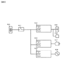
一方、図6に示すように、高電圧バッテリ600、高電圧リレー601に対して、DCDCコンバータ602と並列にインバータ603、車載充電器604が接続されるシステムでは、DCDCコンバータ602が高電圧コンデンサC602を有するのと同様に、インバータ603は高電圧コンデンサC603を有し、車載充電器604は高電圧コンデンサC604を有する。
On the other hand, as shown in FIG. 6, in a system in which an
従来は、DCDCコンバータ602、インバータ603、車載充電器604はそれぞれ高電圧コンデンサC602、C603、C604の放電回路を有する。これに対して本実施例では、DCDCコンバータ602にて、DCDCコンバータ602の高電圧コンデンサC602のみならず、インバータ603、車載充電器604の高電圧コンデンサC603、C604の放電を行う。
Conventionally, the
高電圧コンデンサC602、C603、C604の容量の総和、要求される放電時間t、低下させるべき電圧VIN(A)−VIN(B)を満足できるように、低電圧バッテリ605に出力する電流の制御を行う。 In order to satisfy the sum of the capacities of the high voltage capacitors C602, C603, C604, the required discharge time t, and the voltage VIN (A) −VIN (B) to be reduced, Take control.
電流の制御は、以下のように行う。
上記(3)式より、コンデンサ容量と、低下させるべき電圧高電圧側コンデンサの電圧VIN(A)−VIN(B)の放電時間tより、出力電流指令*Ioを求める。
The current is controlled as follows.
From the above equation (3), the output current command * Io is obtained from the capacitor capacity and the discharge time t of the voltage VIN (A) −VIN (B) of the high voltage side capacitor to be reduced.
次に、図1の電流検出器CT1より出力電流Ioを検出し、出力電流指令*Ioと出力電流Ioの偏差が無くなるように、比例積分演算を行い、指令値Dを求める。 Next, the output current Io is detected by the current detector CT1 in FIG. 1, and a proportional-integral calculation is performed so as to eliminate the deviation between the output current command * Io and the output current Io, thereby obtaining the command value D.
指令値Dを用いて、DCDCコンバータが第1モードで動作するときは、高電圧側スイッチング回路107のMOSFET_Q1〜Q4がスイッチングする周期に対するQ1とQ3が同時にONする期間の比率DHに指令値Dを設定して電流の制御を行う。そして、第2モードで動作するときは、低電圧側スイッチング回路108のMOSFET_Q5〜Q8がスイッチングする周期に対するQ5とQ7が同時にONする期間の比率DLに指定値Dを設定して電流の制御を行う。
When the DCDC converter operates in the first mode using the command value D, the command value D is set to the ratio DH of the period in which Q1 and Q3 are simultaneously turned on with respect to the period in which the MOSFET_Q1 to Q4 of the high voltage
また、上記説明では、具体例として、インバータ603と車載充電器604について記載を行っているが、他の電動製品が複数接続された場合も同様に、高電圧コンデンサの容量と放電時間tの要求に合わせて出力電流を制御し放電を行うことが可能である。例えば、高電圧側コンデンサC1のコンデンサ容量と、高電圧側スイッチング回路107の電流容量に合わせて、低電圧電源である低電圧バッテリー104に出力を行う電流を制御する機能を有している。
In the above description, the
高電圧バッテリ600は、電力貯蔵媒体であり、車載充電器604により充電され、DCDCコンバータ602、インバータ603の電力源となる。
The
高電圧リレー601は、高電圧バッテリ600とDCDCコンバータ602、インバータ603、車載充電器604の間に配置され、高電圧バッテリ600とDCDCコンバータ602、インバータ603、車載充電器604との間の電力の流れを遮断する。DCDCコンバータ602は、高電圧バッテリ600から供給された高電圧を低電圧に変換し、低電圧バッテリ605と低電圧側負荷606に電力を供給する。
The
インバータ603は、高電圧バッテリ600の直流電圧を交流に変換しモータ607に電力を供給する。車載充電器604は、商用系統608から交流電圧を受電し、交流を直流に変換し、高電圧バッテリ600に電力を供給する。低電圧バッテリ605は、電力貯蔵媒体であり、DCDCコンバータ602から電力の供給を受け、低電圧側負荷606へ電力を供給する。低電圧側負荷606は、DCDCコンバータ602や、低電圧バッテリ605より電力の供給を受け動作する負荷装置である。モータ607は、インバータ603から供給された電気エネルギーを機械エネルギーに変換する。
The
商用系統608は、交流電圧源であり、車載充電器に交流電圧を供給する。
高電圧側コンデンサC602は、DCDCコンバータ602内の高電圧入力側に配置され、電圧変動を抑制する。高電圧側コンデンサC603は、インバータ603内の高電圧入力側に配置され、電圧変動を抑制する。高電圧側コンデンサC604は、車載充電器604内の高電圧入力側に配置され、電圧変動を抑制する。
The
The high voltage side capacitor C602 is arranged on the high voltage input side in the
[実施例4]
次に、本発明の実施例4について図7を用いて説明する。なお、実施例1と同様の構成要素には同一の符号を付することでその詳細な説明を省略する。
[Example 4]
Next,
図7は、実施例4におけるDCDCコンバータと周辺機器の構成を説明する図である。
実施例1との違いは、低電圧側スイッチング回路108aの構成と、リアクトルL2をバイパスするスイッチ110にダイオードD9が追加して設けられている点である。本実施例では、絶縁トランスT1と、低電圧側スイッチング回路108と、リアクトルL1がセンタタップ回路を構成しており、リアクトルL1を短絡するスイッチ110に直列にダイオードD9が設けられた構成を有している。
FIG. 7 is a diagram illustrating the configuration of the DCDC converter and peripheral devices in the fourth embodiment.
The difference from the first embodiment is that the diode D9 is additionally provided in the configuration of the low voltage
低電圧側スイッチング回路108aは、絶縁トランスT1より交流矩形波電圧を受電し、MOSFET_Q6a、Q7aをスイッチングする。具体的には、MOSFET_Q1とQ3が同時にONする期間は、MOSFET_Q7aをONし、MOSFET_Q2とQ4が同時にONする期間はMOSFET_Q6aをONして、交流矩形波電圧の整流を行う。ダイオードD9は、本発明にて低電圧側スイッチング回路108aが昇圧コンバータとして動作する際、整流ダイオードとして動作を行う。
The low voltage
本実施例のDCDCコンバータ102は、第1モードでは、高電圧側スイッチング回路107のMOSFET_Q1〜Q4をスイッチングして、高電圧側コンデンサC1の電圧を交流矩形波電圧に変換し、共振リアクトルL1と絶縁トランスT1の一次側に出力する。絶縁トランスT1は、入力された一次側の電圧を絶縁した電圧に変換し、二次側に出力する。絶縁トランスT1の二次側から交流矩形波電圧を受電した低電圧側スイッチング回路108aは、MOSFET_Q6a、Q7aをスイッチングすることで、低損失に交流矩形波電圧の整流を行う。
In the first mode, the
ダイオードD6a、D7aを使用しての整流と比較して、MOSFET_Q6a、Q7aを使用しての整流は導通損失が小さいため、ダイオードD6a、D7aに電流が流れるタイミングでMOSFET_Q6a、Q7aをONし、Q6a、Q7aを導通経路とすることで導通損失を低減している。具体的にはMOSFET_Q1とQ3が同時にONする期間はMOSFET_Q7aをONし、MOSFET_Q2とQ4が同時にONする期間はMOSFET_Q6aをONして、交流矩形波電圧の整流を行う。 Compared with the rectification using the diodes D6a and D7a, the rectification using the MOSFET_Q6a and Q7a has a small conduction loss. By using Q7a as a conduction path, conduction loss is reduced. Specifically, MOSFET_Q7a is turned on during a period in which MOSFET_Q1 and Q3 are simultaneously turned on, and MOSFET_Q6a is turned on in a period in which MOSFET_Q2 and Q4 are simultaneously turned on to rectify the AC rectangular wave voltage.
低電圧側スイッチング回路108aから出力された、整流された矩形波電圧をリアクトルL2とコンデンサC2にて直流平滑化し、低電圧に変換し、低電圧バッテリ104に電力を供給することで、高電圧側コンデンサC1の電圧の放電を行う。
The rectified rectangular wave voltage output from the low voltage
高電圧側コンデンサC1の放電が進み、電圧が低下するのに対して、高電圧側スイッチング回路107のMOSFET_Q1〜Q4のスイッチング周期に対するQ1とQ3、Q2とQ4が同時にONとなる期間DHを長くすることで、出力電圧Voutを低電圧バッテリ104に電力供給可能な高い電圧に制御を行い、高電圧側コンデンサC1の電圧の放電を継続する。
The discharge process progresses the high voltage side capacitor C1, while the voltage decreases, Q1 and Q3, Q2 and Q4 are longer period D H which becomes ON at the same time to the switching cycle of MOSFET_Q1~Q4 the high voltage
図3の点D点に達して、高電圧側コンデンサC1の放電による電圧低下に対して、高電圧側スイッチング回路107のMOSFET_Q1〜Q4のスイッチング周期に対するQ1とQ3、Q2とQ4が同時にONとなる比率DHが最大で飽和すると、出力電圧Voutを低電圧バッテリ104aに電力供給可能な高い電圧に制御を行うことができなくなり、高電圧側コンデンサC1の放電を継続できなくなる(図3の期間5)。
When point D in FIG. 3 is reached, Q1 and Q3 and Q2 and Q4 with respect to the switching period of MOSFET_Q1 to Q4 of the high voltage
図3の期間5にて、高電圧側スイッチング回路107のMOSFET_Q1〜Q4のスイッチング周期に対するMOSFET_Q1とQ3、MOSFET_Q2とQ4が同時にONとなる比率DHの最大値での飽和と、高電圧側コンデンサC1aの電圧低下率の低下を検知して、図3のE点にて第2モードに切り替える。
At time 5 in Fig. 3, MOSFET_Q1 and Q3 to the switching period of MOSFET_Q1~Q4 the high voltage
第2モードとなる図3の期間6では、スイッチ110をONすることで、リアクトルL2が接続されていた箇所にダイオードD9が接続された状態とし、高電圧側スイッチング回路107は、MOSFET_Q1〜Q4のスイッチング周期に対するQ1とQ3、Q2とQ4が同時にONとなる比率DHを最大で固定とし、低電圧側スイッチング回路108aを昇圧型コンバータとして動作させる。
In the period 6 of FIG. 3 that is the second mode, by turning on the
低電圧側スイッチング回路108aの具体的動作を図4(b)と図7を用いて説明を行う。MOSFET_Q1とQ3が同時にONし、絶縁トランスT1に正の電圧が印加されたときには、MOSFET_Q6aをONして、絶縁トランスT1の二次巻線を短絡し、リアクトルL1に電力を蓄積する(図4(b)の期間1)。
A specific operation of the low-voltage
次に、MOSFET_Q1とQ3が同時にONし、絶縁トランスT1に正の電圧が印加された状態のままQ6aをOFFし、リアクトルL1の電力を開放し、ダイオードD9を経由して、低電圧バッテリ104に電力を供給する (図4(b)の期間2)。
Next, MOSFET_Q1 and Q3 are simultaneously turned ON, Q6a is turned OFF while a positive voltage is applied to the isolation transformer T1, the power of the reactor L1 is released, and the
昇圧率を上げるためには、MOSFET_Q1、Q3がONしているときのMOSFET_Q6aのON期間を長くすればよい、つまり、図4(b)の期間1を長くし期間2を短くする。出力を下げるときは、MOSFET_Q6aのON期間を短くすればよい。
In order to increase the step-up ratio, it is only necessary to lengthen the ON period of MOSFET_Q6a when MOSFET_Q1 and Q3 are ON. That is, period 1 in FIG. 4B is lengthened and
図4(b)の期間3、期間4は、期間1、期間2が絶縁トランスT1に印加される電圧が正に対して、絶縁トランスT1に印加される電圧が負になる対称動作であるため説明は省略する。
低電圧側スイッチング回路108aを昇圧型コンバータとして動作させる際は、ダイオードD6a、D7aが導通する期間にQ6a、Q7aをONすることで同期整流を行い、導通損失を低減し、より多くの電力を低電圧バッテリ104aに回収することも可能である。
When operating the low-voltage
以上、本発明の実施形態について詳述したが、本発明は、前記の実施形態に限定されるものではなく、特許請求の範囲に記載された本発明の精神を逸脱しない範囲で、種々の設計変更を行うことができるものである。例えば、前記した実施の形態は本発明を分かりやすく説明するために詳細に説明したものであり、必ずしも説明した全ての構成を備えるものに限定されるものではない。また、ある実施形態の構成の一部を他の実施形態の構成に置き換えることが可能であり、また、ある実施形態の構成に他の実施形態の構成を加えることも可能である。さらに、各実施形態の構成の一部について、他の構成の追加・削除・置換をすることが可能である。 Although the embodiments of the present invention have been described in detail above, the present invention is not limited to the above-described embodiments, and various designs can be made without departing from the spirit of the present invention described in the claims. It can be changed. For example, the above-described embodiment has been described in detail for easy understanding of the present invention, and is not necessarily limited to one having all the configurations described. Further, a part of the configuration of an embodiment can be replaced with the configuration of another embodiment, and the configuration of another embodiment can be added to the configuration of an embodiment. Furthermore, it is possible to add, delete, and replace other configurations for a part of the configuration of each embodiment.
100 高電圧バッテリ
101 高電圧リレー
102 DCDCコンバータ
103 車両ECU
104 低電圧バッテリ
105 低電圧側負荷
106 DCDC制御装置
107 高電圧側スイッチング回路
108 低電圧側スイッチング回路
109 放電回路
110 スイッチ
C1 高電圧側コンデンサ
C2 低電圧側コンデンサ
CT1 電流検出器
D1〜D9 ダイオード
L1、L2 リアクトル
T1 絶縁トランス
Q1〜Q8 MOSFET
VT1、VT2 電圧検出器
DESCRIPTION OF
104
VT1, VT2 voltage detector
Claims (6)
低電圧電源と接続される低電圧側スイッチング回路と、
前記高電圧側スイッチング回路と前記低電圧側スイッチング回路を磁気的に接続するトランスと、
前記高電圧側スイッチング回路に電気的に並列に接続されたコンデンサと、を備え、
前記低電圧側スイッチング回路は、前記コンデンサの電荷を前記トランスを介して前記低電圧電源に放電することを特徴とするDCDCコンバータ。 A high voltage side switching circuit connected to a high voltage power supply;
A low voltage side switching circuit connected to a low voltage power supply;
A transformer for magnetically connecting the high voltage side switching circuit and the low voltage side switching circuit;
A capacitor electrically connected in parallel to the high voltage side switching circuit,
The low-voltage side switching circuit discharges the electric charge of the capacitor to the low-voltage power supply through the transformer.
前記高電圧側スイッチング回路のスイッチング素子のON期間のデューティー比を前記コンデンサの電圧の減少とともに増加させ、
前記低電圧側スイッチング回路のスイッチング素子のON期間のデューティー比を前記高電圧側スイッチング回路のスイッチング素子のON期間のデューティー比に同期させることを特徴とするDCDCコンバータ。 The DCDC converter according to claim 1, wherein
Increasing the duty ratio of the ON period of the switching element of the high voltage side switching circuit as the voltage of the capacitor decreases,
A DCDC converter characterized in that a duty ratio of an ON period of a switching element of the low voltage side switching circuit is synchronized with a duty ratio of an ON period of the switching element of the high voltage side switching circuit.
前記高電圧側スイッチング回路のスイッチング素子のON期間のデューティーを前記コンデンサの電圧の減少とともに増加させる第1モードと、
前記デューティーが所定値となった場合、前記低電圧側スイッチング回路の電圧が前記低電圧電源の電圧より大きくなるように前記低電圧側スイッチング回路の電圧を昇圧させる第2モードと、
を有するDCDCコンバータ。 The DCDC converter according to claim 1, wherein
A first mode in which the duty of the ON period of the switching element of the high-voltage side switching circuit is increased with a decrease in the voltage of the capacitor;
A second mode for boosting the voltage of the low-voltage side switching circuit so that the voltage of the low-voltage side switching circuit is greater than the voltage of the low-voltage power supply when the duty is a predetermined value;
DCDC converter having
前記コンデンサの容量と、前記スイッチの電流容量に合わせて、
前記低電圧電源に出力を行う電流を制御する機能を有するDCDCコンバータ。 The DCDC converter according to claim 1 or 2,
According to the capacity of the capacitor and the current capacity of the switch,
A DCDC converter having a function of controlling a current output to the low voltage power source.
前記トランスと前記低電圧側スイッチング回路と、リアクトルがセンタタップ回路を構成し、前記リアクトルを短絡するスイッチと直列にダイオードを備えたDCDCコンバータ。 The DCDC converter according to claim 1 or 2,
A DCDC converter including a diode in series with a switch that short-circuits the reactor, the transformer, the low-voltage side switching circuit, and a reactor forming a center tap circuit.
Priority Applications (1)
| Application Number | Priority Date | Filing Date | Title |
|---|---|---|---|
| JP2016000332A JP2017123703A (en) | 2016-01-05 | 2016-01-05 | Dc-dc converter |
Applications Claiming Priority (1)
| Application Number | Priority Date | Filing Date | Title |
|---|---|---|---|
| JP2016000332A JP2017123703A (en) | 2016-01-05 | 2016-01-05 | Dc-dc converter |
Publications (1)
| Publication Number | Publication Date |
|---|---|
| JP2017123703A true JP2017123703A (en) | 2017-07-13 |
Family
ID=59306757
Family Applications (1)
| Application Number | Title | Priority Date | Filing Date |
|---|---|---|---|
| JP2016000332A Pending JP2017123703A (en) | 2016-01-05 | 2016-01-05 | Dc-dc converter |
Country Status (1)
| Country | Link |
|---|---|
| JP (1) | JP2017123703A (en) |
Cited By (3)
| Publication number | Priority date | Publication date | Assignee | Title |
|---|---|---|---|---|
| JP2019149867A (en) * | 2018-02-26 | 2019-09-05 | オムロン株式会社 | Power converter and power conversion system |
| JP2019149866A (en) * | 2018-02-26 | 2019-09-05 | オムロン株式会社 | Power converter and power conversion system |
| CN114301040A (en) * | 2021-09-26 | 2022-04-08 | 华为数字能源技术有限公司 | Discharging method of bus capacitor and related equipment thereof |
-
2016
- 2016-01-05 JP JP2016000332A patent/JP2017123703A/en active Pending
Cited By (4)
| Publication number | Priority date | Publication date | Assignee | Title |
|---|---|---|---|---|
| JP2019149867A (en) * | 2018-02-26 | 2019-09-05 | オムロン株式会社 | Power converter and power conversion system |
| JP2019149866A (en) * | 2018-02-26 | 2019-09-05 | オムロン株式会社 | Power converter and power conversion system |
| CN114301040A (en) * | 2021-09-26 | 2022-04-08 | 华为数字能源技术有限公司 | Discharging method of bus capacitor and related equipment thereof |
| WO2023045781A1 (en) * | 2021-09-26 | 2023-03-30 | 华为数字能源技术有限公司 | Discharging method of bus capacitor and related device thereof |
Similar Documents
| Publication | Publication Date | Title |
|---|---|---|
| EP2978118B1 (en) | Power converter and power conditioner | |
| US10541549B2 (en) | Power supply apparatus | |
| CN107408889B (en) | Power converter | |
| US10461553B2 (en) | Power source device | |
| US11616451B2 (en) | Pre-chargeable DCDC conversion circuit | |
| RU2473159C1 (en) | Electric capacity converter | |
| JP5680050B2 (en) | Charger | |
| US20120313572A1 (en) | Integrated buck-boost converter of charging apparatus | |
| WO2015096613A1 (en) | Online interactive uninterruptible power supply and control method therefor | |
| JP2018170930A (en) | Power conversion device and power conversion system | |
| JP3699082B2 (en) | Switching power supply circuit | |
| KR20150067510A (en) | Apparatus and Method for controlling charge for battery | |
| US8830701B2 (en) | DC-DC converter | |
| JP5347362B2 (en) | Emergency power circuit | |
| JP2005102476A (en) | Activation method for power conversion device | |
| JP2017123703A (en) | Dc-dc converter | |
| JP6327403B2 (en) | Energy management system | |
| US11095156B2 (en) | Power conversion device and non-contact power supplying system | |
| US11050353B2 (en) | Power conversion device that generates switching signals | |
| KR101516899B1 (en) | Power conversion apparatus for vehicle and Method for controling the same | |
| JP2017038424A (en) | Power conversion device | |
| JP5831275B2 (en) | Power converter and driving method thereof | |
| KR101643705B1 (en) | Apparatus and method for controlling ups | |
| JP2016158353A (en) | Power conversion device | |
| JP6915566B2 (en) | Power converter and power conversion system |