JP2016510941A - Multi-layer battery electrode design to enable thicker electrode manufacturing - Google Patents
Multi-layer battery electrode design to enable thicker electrode manufacturing Download PDFInfo
- Publication number
- JP2016510941A JP2016510941A JP2016500667A JP2016500667A JP2016510941A JP 2016510941 A JP2016510941 A JP 2016510941A JP 2016500667 A JP2016500667 A JP 2016500667A JP 2016500667 A JP2016500667 A JP 2016500667A JP 2016510941 A JP2016510941 A JP 2016510941A
- Authority
- JP
- Japan
- Prior art keywords
- slurry mixture
- cathode
- layer
- material layer
- active material
- Prior art date
- Legal status (The legal status is an assumption and is not a legal conclusion. Google has not performed a legal analysis and makes no representation as to the accuracy of the status listed.)
- Pending
Links
Images


Classifications
-
- H—ELECTRICITY
- H01—ELECTRIC ELEMENTS
- H01M—PROCESSES OR MEANS, e.g. BATTERIES, FOR THE DIRECT CONVERSION OF CHEMICAL ENERGY INTO ELECTRICAL ENERGY
- H01M4/00—Electrodes
- H01M4/02—Electrodes composed of, or comprising, active material
- H01M4/36—Selection of substances as active materials, active masses, active liquids
- H01M4/362—Composites
- H01M4/366—Composites as layered products
-
- H—ELECTRICITY
- H01—ELECTRIC ELEMENTS
- H01M—PROCESSES OR MEANS, e.g. BATTERIES, FOR THE DIRECT CONVERSION OF CHEMICAL ENERGY INTO ELECTRICAL ENERGY
- H01M4/00—Electrodes
- H01M4/02—Electrodes composed of, or comprising, active material
- H01M4/04—Processes of manufacture in general
- H01M4/0402—Methods of deposition of the material
- H01M4/0404—Methods of deposition of the material by coating on electrode collectors
-
- H—ELECTRICITY
- H01—ELECTRIC ELEMENTS
- H01M—PROCESSES OR MEANS, e.g. BATTERIES, FOR THE DIRECT CONVERSION OF CHEMICAL ENERGY INTO ELECTRICAL ENERGY
- H01M4/00—Electrodes
- H01M4/02—Electrodes composed of, or comprising, active material
- H01M4/04—Processes of manufacture in general
- H01M4/0402—Methods of deposition of the material
- H01M4/0409—Methods of deposition of the material by a doctor blade method, slip-casting or roller coating
-
- H—ELECTRICITY
- H01—ELECTRIC ELEMENTS
- H01M—PROCESSES OR MEANS, e.g. BATTERIES, FOR THE DIRECT CONVERSION OF CHEMICAL ENERGY INTO ELECTRICAL ENERGY
- H01M4/00—Electrodes
- H01M4/02—Electrodes composed of, or comprising, active material
- H01M4/04—Processes of manufacture in general
- H01M4/043—Processes of manufacture in general involving compressing or compaction
- H01M4/0435—Rolling or calendering
-
- H—ELECTRICITY
- H01—ELECTRIC ELEMENTS
- H01M—PROCESSES OR MEANS, e.g. BATTERIES, FOR THE DIRECT CONVERSION OF CHEMICAL ENERGY INTO ELECTRICAL ENERGY
- H01M4/00—Electrodes
- H01M4/02—Electrodes composed of, or comprising, active material
- H01M4/13—Electrodes for accumulators with non-aqueous electrolyte, e.g. for lithium-accumulators; Processes of manufacture thereof
- H01M4/131—Electrodes based on mixed oxides or hydroxides, or on mixtures of oxides or hydroxides, e.g. LiCoOx
-
- H—ELECTRICITY
- H01—ELECTRIC ELEMENTS
- H01M—PROCESSES OR MEANS, e.g. BATTERIES, FOR THE DIRECT CONVERSION OF CHEMICAL ENERGY INTO ELECTRICAL ENERGY
- H01M4/00—Electrodes
- H01M4/02—Electrodes composed of, or comprising, active material
- H01M4/13—Electrodes for accumulators with non-aqueous electrolyte, e.g. for lithium-accumulators; Processes of manufacture thereof
- H01M4/136—Electrodes based on inorganic compounds other than oxides or hydroxides, e.g. sulfides, selenides, tellurides, halogenides or LiCoFy
-
- H—ELECTRICITY
- H01—ELECTRIC ELEMENTS
- H01M—PROCESSES OR MEANS, e.g. BATTERIES, FOR THE DIRECT CONVERSION OF CHEMICAL ENERGY INTO ELECTRICAL ENERGY
- H01M4/00—Electrodes
- H01M4/02—Electrodes composed of, or comprising, active material
- H01M4/13—Electrodes for accumulators with non-aqueous electrolyte, e.g. for lithium-accumulators; Processes of manufacture thereof
- H01M4/139—Processes of manufacture
- H01M4/1391—Processes of manufacture of electrodes based on mixed oxides or hydroxides, or on mixtures of oxides or hydroxides, e.g. LiCoOx
-
- H—ELECTRICITY
- H01—ELECTRIC ELEMENTS
- H01M—PROCESSES OR MEANS, e.g. BATTERIES, FOR THE DIRECT CONVERSION OF CHEMICAL ENERGY INTO ELECTRICAL ENERGY
- H01M4/00—Electrodes
- H01M4/02—Electrodes composed of, or comprising, active material
- H01M4/13—Electrodes for accumulators with non-aqueous electrolyte, e.g. for lithium-accumulators; Processes of manufacture thereof
- H01M4/139—Processes of manufacture
- H01M4/1397—Processes of manufacture of electrodes based on inorganic compounds other than oxides or hydroxides, e.g. sulfides, selenides, tellurides, halogenides or LiCoFy
-
- H—ELECTRICITY
- H01—ELECTRIC ELEMENTS
- H01M—PROCESSES OR MEANS, e.g. BATTERIES, FOR THE DIRECT CONVERSION OF CHEMICAL ENERGY INTO ELECTRICAL ENERGY
- H01M4/00—Electrodes
- H01M4/02—Electrodes composed of, or comprising, active material
- H01M4/36—Selection of substances as active materials, active masses, active liquids
- H01M4/362—Composites
- H01M4/364—Composites as mixtures
-
- H—ELECTRICITY
- H01—ELECTRIC ELEMENTS
- H01M—PROCESSES OR MEANS, e.g. BATTERIES, FOR THE DIRECT CONVERSION OF CHEMICAL ENERGY INTO ELECTRICAL ENERGY
- H01M4/00—Electrodes
- H01M4/02—Electrodes composed of, or comprising, active material
- H01M4/36—Selection of substances as active materials, active masses, active liquids
- H01M4/48—Selection of substances as active materials, active masses, active liquids of inorganic oxides or hydroxides
- H01M4/485—Selection of substances as active materials, active masses, active liquids of inorganic oxides or hydroxides of mixed oxides or hydroxides for inserting or intercalating light metals, e.g. LiTi2O4 or LiTi2OxFy
-
- H—ELECTRICITY
- H01—ELECTRIC ELEMENTS
- H01M—PROCESSES OR MEANS, e.g. BATTERIES, FOR THE DIRECT CONVERSION OF CHEMICAL ENERGY INTO ELECTRICAL ENERGY
- H01M4/00—Electrodes
- H01M4/02—Electrodes composed of, or comprising, active material
- H01M4/36—Selection of substances as active materials, active masses, active liquids
- H01M4/48—Selection of substances as active materials, active masses, active liquids of inorganic oxides or hydroxides
- H01M4/50—Selection of substances as active materials, active masses, active liquids of inorganic oxides or hydroxides of manganese
- H01M4/505—Selection of substances as active materials, active masses, active liquids of inorganic oxides or hydroxides of manganese of mixed oxides or hydroxides containing manganese for inserting or intercalating light metals, e.g. LiMn2O4 or LiMn2OxFy
-
- H—ELECTRICITY
- H01—ELECTRIC ELEMENTS
- H01M—PROCESSES OR MEANS, e.g. BATTERIES, FOR THE DIRECT CONVERSION OF CHEMICAL ENERGY INTO ELECTRICAL ENERGY
- H01M4/00—Electrodes
- H01M4/02—Electrodes composed of, or comprising, active material
- H01M4/36—Selection of substances as active materials, active masses, active liquids
- H01M4/48—Selection of substances as active materials, active masses, active liquids of inorganic oxides or hydroxides
- H01M4/52—Selection of substances as active materials, active masses, active liquids of inorganic oxides or hydroxides of nickel, cobalt or iron
- H01M4/525—Selection of substances as active materials, active masses, active liquids of inorganic oxides or hydroxides of nickel, cobalt or iron of mixed oxides or hydroxides containing iron, cobalt or nickel for inserting or intercalating light metals, e.g. LiNiO2, LiCoO2 or LiCoOxFy
-
- H—ELECTRICITY
- H01—ELECTRIC ELEMENTS
- H01M—PROCESSES OR MEANS, e.g. BATTERIES, FOR THE DIRECT CONVERSION OF CHEMICAL ENERGY INTO ELECTRICAL ENERGY
- H01M4/00—Electrodes
- H01M4/02—Electrodes composed of, or comprising, active material
- H01M4/36—Selection of substances as active materials, active masses, active liquids
- H01M4/58—Selection of substances as active materials, active masses, active liquids of inorganic compounds other than oxides or hydroxides, e.g. sulfides, selenides, tellurides, halogenides or LiCoFy; of polyanionic structures, e.g. phosphates, silicates or borates
- H01M4/5825—Oxygenated metallic salts or polyanionic structures, e.g. borates, phosphates, silicates, olivines
-
- H—ELECTRICITY
- H01—ELECTRIC ELEMENTS
- H01M—PROCESSES OR MEANS, e.g. BATTERIES, FOR THE DIRECT CONVERSION OF CHEMICAL ENERGY INTO ELECTRICAL ENERGY
- H01M4/00—Electrodes
- H01M4/02—Electrodes composed of, or comprising, active material
- H01M4/62—Selection of inactive substances as ingredients for active masses, e.g. binders, fillers
- H01M4/621—Binders
- H01M4/622—Binders being polymers
- H01M4/623—Binders being polymers fluorinated polymers
-
- H—ELECTRICITY
- H01—ELECTRIC ELEMENTS
- H01M—PROCESSES OR MEANS, e.g. BATTERIES, FOR THE DIRECT CONVERSION OF CHEMICAL ENERGY INTO ELECTRICAL ENERGY
- H01M4/00—Electrodes
- H01M4/02—Electrodes composed of, or comprising, active material
- H01M4/64—Carriers or collectors
- H01M4/66—Selection of materials
- H01M4/661—Metal or alloys, e.g. alloy coatings
-
- H—ELECTRICITY
- H01—ELECTRIC ELEMENTS
- H01M—PROCESSES OR MEANS, e.g. BATTERIES, FOR THE DIRECT CONVERSION OF CHEMICAL ENERGY INTO ELECTRICAL ENERGY
- H01M4/00—Electrodes
- H01M4/02—Electrodes composed of, or comprising, active material
- H01M2004/021—Physical characteristics, e.g. porosity, surface area
-
- H—ELECTRICITY
- H01—ELECTRIC ELEMENTS
- H01M—PROCESSES OR MEANS, e.g. BATTERIES, FOR THE DIRECT CONVERSION OF CHEMICAL ENERGY INTO ELECTRICAL ENERGY
- H01M4/00—Electrodes
- H01M4/02—Electrodes composed of, or comprising, active material
- H01M2004/026—Electrodes composed of, or comprising, active material characterised by the polarity
- H01M2004/028—Positive electrodes
-
- Y—GENERAL TAGGING OF NEW TECHNOLOGICAL DEVELOPMENTS; GENERAL TAGGING OF CROSS-SECTIONAL TECHNOLOGIES SPANNING OVER SEVERAL SECTIONS OF THE IPC; TECHNICAL SUBJECTS COVERED BY FORMER USPC CROSS-REFERENCE ART COLLECTIONS [XRACs] AND DIGESTS
- Y02—TECHNOLOGIES OR APPLICATIONS FOR MITIGATION OR ADAPTATION AGAINST CLIMATE CHANGE
- Y02E—REDUCTION OF GREENHOUSE GAS [GHG] EMISSIONS, RELATED TO ENERGY GENERATION, TRANSMISSION OR DISTRIBUTION
- Y02E60/00—Enabling technologies; Technologies with a potential or indirect contribution to GHG emissions mitigation
- Y02E60/10—Energy storage using batteries
Abstract
本発明の実施形態は一般に、高容量エネルギー貯蔵デバイスならびに高容量エネルギー貯蔵デバイスを製造するための方法および装置に関する。一実施形態では、多層カソード構造体を形成するための方法が提供される。方法は、導電性基板を提供することと、カソード活物質を含む第1のスラリ混合物を堆積させて導電性基板上に第1のカソード材料層を形成することと、カソード活物質を含む第2のスラリ混合物を堆積させて第1のカソード材料層上に第2のカソード材料層を形成することと、堆積されたままの状態の第1のカソード材料層と第2のカソード材料層を圧縮して所望の多孔度を達成することを含む。【選択図】図4DEmbodiments of the invention generally relate to high capacity energy storage devices and methods and apparatus for manufacturing high capacity energy storage devices. In one embodiment, a method for forming a multilayer cathode structure is provided. The method provides a conductive substrate, deposits a first slurry mixture that includes a cathode active material to form a first cathode material layer on the conductive substrate, and a second that includes a cathode active material. Forming a second cathode material layer on the first cathode material layer and compressing the as-deposited first cathode material layer and the second cathode material layer. Achieving the desired porosity. [Selection] Figure 4D
Description
本発明の実施形態は一般に、高容量エネルギー貯蔵デバイスならびに高容量エネルギー貯蔵デバイスを製造するための方法および装置に関する。 Embodiments of the present invention generally relate to high capacity energy storage devices and methods and apparatus for manufacturing high capacity energy storage devices.
超コンデンサやリチウムイオン(Li−ion)電池などの急速充電、高容量エネルギー貯蔵デバイスは、携帯用電子機器や、医用、輸送、グリッド接続される大エネルギー貯蔵、再生可能エネルギー貯蔵、無停電電源(UPS)を含め、ますます多くの用途で使用されている。 Rapid charging and high-capacity energy storage devices such as supercapacitors and lithium-ion (Li-ion) batteries are used in portable electronic devices, medical, transportation, grid-connected large energy storage, renewable energy storage, uninterruptible power supplies ( Are being used in an increasing number of applications, including UPS.
現在の再充電可能な二次的エネルギー貯蔵デバイスは典型的に、アノード電極、カソード電極、アノード電極とカソード電極との間に位置されるセパレータ、および少なくとも1つの集電体を含む。正極集電体(カソード)の材料の例には典型的に、アルミニウム(Al)、ステンレス鋼(SST)、およびニッケル(Ni)がある。負極集電体(アノード)の材料の例には典型的に銅(Cu)があるが、ステンレス鋼(SST)やニッケル(Ni)が使用されてもよい。 Current rechargeable secondary energy storage devices typically include an anode electrode, a cathode electrode, a separator positioned between the anode and cathode electrodes, and at least one current collector. Examples of materials for the positive electrode current collector (cathode) typically include aluminum (Al), stainless steel (SST), and nickel (Ni). An example of the material of the negative electrode current collector (anode) is typically copper (Cu), but stainless steel (SST) or nickel (Ni) may be used.
Li−ion電池のカソード活物質は典型的に、広範囲のリチウム遷移金属酸化物から選択される。例には、酸化物のうちスピネル型構造を持つもの(LiMn2O4(LMO)、LiNi0.5Mn1.5O4(LMNO))、層状構造を持つもの(LiCoO2、ニッケルマンガンコバルト酸リチウム(NMC)、ニッケルコバルトアルミニウム酸リチウム(NCA))、オリビン型構造を持つもの(たとえば、LiFePO4)、およびそれらの組合せがある。 The cathode active material of a Li-ion battery is typically selected from a wide range of lithium transition metal oxides. Examples include oxides having a spinel structure (LiMn 2 O 4 (LMO), LiNi 0.5 Mn 1.5 O 4 (LMNO)), and those having a layered structure (LiCoO 2 , nickel manganese cobalt). Lithium acid lithium (NMC), nickel cobalt lithium aluminum oxide (NCA)), those with an olivine structure (eg, LiFePO 4 ), and combinations thereof.
アノード活物質は一般に、粒径が約5〜15μmの、黒鉛か硬質炭素かどちらかの炭素系である。シリコン(Si)やスズ(Sn)系の活物質が現在、次世代アノード材料として開発されている。両方とも炭素系電極よりも有意に高い容量を有する。Li15Si4が約3,580mAh/gの容量を有する一方で、黒鉛は372mAh/gよりも小さい容量を有する。Sn系アノードは900mAh/g超の容量を達成でき、これはたいていのカソード材料が達成できるものよりもはるかに高い。それゆえ、カソードは平衡リチウムイオンセルにおいてアノードよりも重くあり続けるであろうことが予想される。 The anode active material is generally a carbon system, either graphite or hard carbon, having a particle size of about 5-15 μm. Silicon (Si) and tin (Sn) -based active materials are currently being developed as next-generation anode materials. Both have significantly higher capacities than carbon-based electrodes. Li 15 Si 4 has a capacity of about 3,580 mAh / g, while graphite has a capacity of less than 372 mAh / g. Sn-based anodes can achieve capacities greater than 900 mAh / g, which is much higher than can be achieved with most cathode materials. Therefore, it is expected that the cathode will continue to be heavier than the anode in the balanced lithium ion cell.
現在、活物質は電池セルの全構成要素のうちの50重量%未満を占めるのみである。より多くの活物質を含有するより厚い電極を製作する能力は、不活性要素からの寄与率を低減することにより、電池エネルギー密度を有意に増加させ、電池セルの生産費用を低減するであろう。しかしながら現在、電極の厚さは、現在使用される材料の利用率と機械的性質の両方により制限される。 Currently, the active material only accounts for less than 50% by weight of the total components of the battery cell. The ability to produce thicker electrodes containing more active material will significantly increase battery energy density and reduce battery cell production costs by reducing the contribution from inert elements. . Currently, however, the thickness of the electrode is limited by both the utilization and mechanical properties of currently used materials.
したがって当該技術分野には、より小さくてより軽い、かつより費用効果的に高い生産速度で製作され得るより急速充電、より高容量エネルギー貯蔵デバイスへの要望がある。 Accordingly, there is a need in the art for faster charging, higher capacity energy storage devices that can be fabricated at smaller, lighter, and more cost effective production rates.
本発明の実施形態は一般に、高容量エネルギー貯蔵デバイスならびに高容量エネルギー貯蔵デバイスを製造するための方法および装置に関する。一実施形態では、多層カソード構造体を形成するための方法が提供される。方法は、導電性基板を提供することと、カソード活物質を含む第1のスラリ混合物を堆積させて導電性基板上に第1のカソード材料層を形成することと、カソード活物質を含む第2のスラリ混合物を堆積させて第1のカソード材料層上に第2のカソード材料層を形成することと、堆積されたままの状態の第1のカソード材料層と第2のカソード材料層を圧縮して所望の多孔度を達成することを含む。 Embodiments of the present invention generally relate to high capacity energy storage devices and methods and apparatus for manufacturing high capacity energy storage devices. In one embodiment, a method for forming a multilayer cathode structure is provided. The method provides a conductive substrate, deposits a first slurry mixture that includes a cathode active material to form a first cathode material layer on the conductive substrate, and a second that includes a cathode active material. Forming a second cathode material layer on the first cathode material layer and compressing the as-deposited first cathode material layer and the second cathode material layer. Achieving the desired porosity.
本発明の上述の特徴が詳細に理解され得るように、上記簡約された本発明のより具体的な説明が、実施形態を参照することによりなされてよく、そのうちのいくつかは添付図面に例示される。添付図面は本発明の典型的な実施形態のみを例示し、したがってその範囲を限定すると見なされるべきではなく、本発明は他の同様に効果的な実施形態を許容してよいとすることに留意されたい。 In order that the above features of the present invention may be understood in detail, a more specific description of the above-described simplified invention may be made by reference to the embodiments, some of which are illustrated in the accompanying drawings. The It should be noted that the accompanying drawings illustrate only typical embodiments of the invention and are therefore not to be considered limiting of the scope thereof, and that the invention may allow other equally effective embodiments. I want to be.
理解を容易にするため、図面に共通である同一の要素を示すために、可能な場合は同一の参照番号が使用される。一実施形態で開示される要素は、具体的な明記なく、他の実施形態で有益に利用されてよいことが企図される。 To facilitate understanding, identical reference numerals have been used, where possible, to designate identical elements that are common to the drawings. It is contemplated that elements disclosed in one embodiment may be beneficially utilized in other embodiments without specific specification.
本発明の実施形態は一般に、高容量エネルギー貯蔵デバイスならびに高容量エネルギー貯蔵デバイスを製造するための方法および装置に関する。高エネルギー密度電池の1つの典型的なカソード材料はLi(NixMnyCoz)O2(X+Y+Z=1)、たとえば、ニッケルマンガンコバルト酸リチウムすなわち「NMC」である。アノード材料は典型的に黒鉛系である。NMCおよび黒鉛電極の両方は多孔性であり、典型的な多孔度が25から35%の間の範囲にある。多孔空間は電解質で満たされてよい。例証的な電解質は、炭酸エチル/炭酸ジエチル「EC/DEC」溶媒およびLiPF6塩などの溶媒とリチウム塩を含有してよい。放電処理の間、Liイオンがリチウム化黒鉛粒子から拡散する。Liイオンは次いで黒鉛粒子間の多孔空間を満たす電解質を通っておよびセパレータを通って拡散し、カソードに到達する。Liイオンは次いでカソード粒子間の電解質を通って拡散し、最終的にカソード粒子間に入る。 Embodiments of the present invention generally relate to high capacity energy storage devices and methods and apparatus for manufacturing high capacity energy storage devices. One typical cathode material for high energy density batteries is Li (Ni x Mn y Co z ) O 2 (X + Y + Z = 1), for example, lithium nickel manganese cobaltate or “NMC”. The anode material is typically graphite-based. Both NMC and graphite electrodes are porous with typical porosity in the range between 25 and 35%. The porous space may be filled with an electrolyte. Exemplary electrolytes may contain solvents and lithium salts, such as ethyl carbonate / diethyl carbonate “EC / DEC” solvents and LiPF 6 salts. During the discharge treatment, Li ions diffuse from the lithiated graphite particles. The Li ions then diffuse through the electrolyte filling the porous space between the graphite particles and through the separator to reach the cathode. The Li ions then diffuse through the electrolyte between the cathode particles and eventually enter between the cathode particles.
電池セルエネルギー密度を増加させるため、電極ローディング(mAh/cm2)を増加させるために、より多くの材料を各電池セルに「詰め込む」ことが非常に望ましい。電極負荷を増加させるための1つの方法は、単位電極面積当たりの活物質の量を増加させること、すなわちより厚い電極を作製および/または電極材料の密度を増加させることである。しかしながら、より厚い電極を生産するための現在の生産処理は煩雑であるのみならずまた接着不足、凝集不足およびサイクル疲労を被る電極を生産する。 In order to increase battery cell energy density, it is highly desirable to “pack” more material into each battery cell in order to increase electrode loading (mAh / cm 2 ). One way to increase the electrode load is to increase the amount of active material per unit electrode area, i.e. make a thicker electrode and / or increase the density of the electrode material. However, current production processes for producing thicker electrodes are not only cumbersome, but also produce electrodes that suffer from poor adhesion, insufficient cohesion and cycle fatigue.
本明細書に記載の特定の実施形態では、より厚い電極製造を可能にするための多層電池電極設計が提供される。特定の実施形態では、より厚い/より高密度の電極が提供されるのみならずまたより厚い電極を低減された生産時間で生産するための処理も提供される。特定の実施形態では、多層電極は各層で異なる性質(たとえば、多孔度、表面積、電極組成物)を有する、または多層電極は各層で異なる活物質化学的性質を有する。たとえば多層電極の層は、各層を形成するために使用されるスラリ組成物、各層の多孔度、各層を形成するために使用される活物質、活物質粒子の粒径、各層中の粒子のモード粒径分布、および活物質のタップ密度のうちの少なくとも1つで他の層に比べて異なってよい。 In certain embodiments described herein, a multilayer battery electrode design is provided to enable thicker electrode manufacturing. In certain embodiments, not only are thicker / higher density electrodes provided, but also a process for producing thicker electrodes with reduced production times. In certain embodiments, the multilayer electrode has different properties (eg, porosity, surface area, electrode composition) in each layer, or the multilayer electrode has different active material chemistry in each layer. For example, the layers of a multi-layer electrode may include the slurry composition used to form each layer, the porosity of each layer, the active material used to form each layer, the particle size of the active material particles, the mode of the particles in each layer It may be different from other layers in at least one of the particle size distribution and the tap density of the active material.
本明細書に記載のこれらの多層電池電極設計は、均一な性質を有する単層電極と比較して(i)より高電力で(ii)より長いサイクルを生ずるであろうと考えられる。 It is believed that these multilayer battery electrode designs described herein will result in (ii) higher power and (ii) longer cycles compared to single layer electrodes having uniform properties.
いくつかの実施形態は2層構造体として論じられるが、本明細書に記載の多孔カソード構造体を形成するために、異なる材料、粒径、および/または密度を含む任意の数の層が使用されてよいことを理解されたい。両面電極が形成される特定の実施形態では、各多孔層は両面堆積処理を用いて基板の両側に同時に堆積されてよい。 Although some embodiments are discussed as a two-layer structure, any number of layers including different materials, particle sizes, and / or densities may be used to form the porous cathode structures described herein. Please understand that it may be. In certain embodiments where double-sided electrodes are formed, each porous layer may be deposited simultaneously on both sides of the substrate using a double-sided deposition process.
本明細書に記載の多層電極設計は以下の電極構造体を含む:(i)各層で異なるスラリ組成物を含み、層間で異なる多孔度をもたらす2つ以上の電極層、(ii)各層で異なる活物質を含む2つ以上の電極層、(iii)各層で同じ活物質の異なる粒径を含み、層間で異なる表面積および/または異なる多孔度をもたらす2つ以上の電極層、(iv)層間で異なる粒径分布(たとえば、単モード、双モード、多モード)を含む2つ以上の電極層、(v)各層で異なる電極組成物(バインダ、導電性添加物、活物質)を含む2つ以上の電極層、(vi)異なるタップ密度の材料を有する2つ以上の電極層、および(i)〜(vi)の任意の組合せ。異なる処理技法が、(i)〜(vi)で列記される層を形成するために使用されてもよい。 The multilayer electrode design described herein includes the following electrode structures: (i) two or more electrode layers that include different slurry compositions in each layer, resulting in different porosities between layers, (ii) different in each layer Two or more electrode layers comprising an active material, (iii) two or more electrode layers comprising different particle sizes of the same active material in each layer, resulting in different surface areas and / or different porosities between layers, (iv) between layers Two or more electrode layers containing different particle size distributions (eg single mode, bimode, multimode), (v) two or more electrode compositions containing different electrode compositions (binders, conductive additives, active materials) in each layer Electrode layers, (vi) two or more electrode layers having different tap density materials, and any combination of (i)-(vi). Different processing techniques may be used to form the layers listed in (i)-(vi).
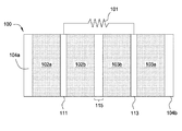
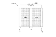
図1Aは、本明細書に記載の実施形態に従って形成される1つまたは複数の電極構造体(アノード102a、102bおよび/またはカソード103a、103b)を有する両面電極を持つ部分電池セル100の概要図である。部分電池セル二重層100はLi−ion電池セル二重層であってよい。カソード構造体103(103aおよび103b)は本明細書に記載の多層電極構造体のうちのいずれかであってよい。図1Bは、本明細書に記載の実施形態に従って形成される1つまたは複数の電極構造体を有する部分電池セル120の概略図である。部分電池セル二重層120はLi−ion電池セル二重層であってよい。電池セル100、120は、本明細書に記載の一実施形態に従って、負荷101に電気的に接続される。電池セル二重層100の主要な機能構成要素には、アノード構造体102a、102b、カソード構造体103a、103b、セパレータ層104a、104bおよび115、集電体111および113、ならびに任意選択で、セパレータ層104a、104bの間の領域内に設けられる電解質(図示せず)がある。電池セル120の主要な機能構成要素には、アノード構造体102b、カソード構造体103b、セパレータ115、集電体111および113、ならびに集電体111、113の間の領域内に設けられる任意選択の電解質(図示せず)がある。様々な材料、たとえば有機溶媒中のリチウム塩が電解質として使用されてよい。電池セル100、120は、集電体111および113のための導線を持つ適切なパッケージに気密に密封されてよい。
FIG. 1A is a schematic diagram of a
アノード構造体102a、102b、カソード構造体103a、103b、ならびにセパレータ層104a、104bおよび115は、セパレータ層104aおよび104bの間に形成される領域で電解質に浸漬されてよい。部分的な例証的な構造が示されること、および特定の実施形態では、追加のアノード構造体、カソード構造体、および集電体がその構造に追加されてよいことを理解されたい。
The
アノード構造体102bは、金属アノード集電体111および本明細書に記載の実施形態に従って形成される活物質を含んでよい。アノード構造体は多孔性であってよい。他の例証的な活物質には、黒鉛状炭素、リチウム、スズ、シリコン、アルミニウム、アンチモン、スズ−ホウ素−コバルト酸化物、およびリチウム−コバルト窒化物(たとえば、Li3−2xCoxN(0.1≦x≦0.44))がある。同様にカソード構造体103bは、それぞれのカソード集電体113および本明細書に記載の実施形態に従って形成される第2の活物質を含んでよい。集電体111および113は金属などの導電性材料で作製される。一実施形態では、アノード集電体111は銅を含み、カソード集電体113はアルミニウムを含む。セパレータ115は、アノード構造体102bとカソード構造体103bの構成要素間の直接的な電気的接触を防止するために使用される。セパレータ115は多孔性であってよい。
The
電池セル100、120のカソード側すなわち正極の活物質は、二酸化コバルトリチウム(LiCoO2)または二酸化マンガンリチウム(LiMnO2)や、LiCoO2、LiNiO2、LiNixCoyO2(たとえば、LiNi0.8Co0.2O2)、LiNixCoyAlzO2(たとえば、LiNi0.8Co0.15Al0.05O2)、LiMn2O4、LixMgyMnzO4(たとえば、LiMg0.5Mn1.5O4)、LiNixMnyO2(たとえば、LiNi0.5Mn1.5O4)、LiNixMnyCozO2(たとえば、LiNiMnCoO2)(NMC)、アルミニウムマンガン酸リチウム(たとえば、LiAlxMnyO4)、LiFePO4などのリチウム含有金属酸化物を含んでよい。活物質は、コバルト酸リチウムなどの層状酸化物、リン酸鉄リチウムなどのオリビン、またはマンガン酸リチウムなどのスピネルから作製されてよい。非リチウムの実施形態では、例証的なカソードはTiS2(二硫化チタン)から作製されてよい。例証的なリチウム含有酸化物は、コバルト酸リチウム(LiCoO2)などの層状、またはLiNixCo1−2xMnxO2や、LiNi0.5Mn1.5O4、Li(Ni0.8Co0.15Al0.05)O2、LiMn2O4などの混合金属酸化物であってよい。例証的なリン酸塩は、鉄オリビン(LiFePO4)およびそのバリアント(LiFe1−xMgxPO4など)、LiMoPO4、LiCoPO4、LiNiPO4、Li3V2(PO4)3、LiVOPO4、LiMP2O7、またはLiFe1.5P2O7であってよい。例証的なフルオロリン酸塩はLiVPO4F、LiAlPO4F、Li5V(PO4)2F2、Li5Cr(PO4)2F2、Li2CoPO4F、またはLi2NiPO4Fであってよい。例証的なケイ酸塩はLi2FeSiO4、Li2MnSiO4、またはLi2VOSiO4であってよい。例証的な非リチウム化合物はNa5V2(PO4)2F3である。
The active material on the cathode side of the
電池セル100、120のアノード側すなわち負極の活物質は、たとえば黒鉛材料および/または様々な細粉、ならびにたとえばマイクロスケールまたはナノスケールサイズの粉末などの材料から作製されてよい。加えて、シリコン、スズ、またはチタン酸リチウム(Li4Ti5O12)が、導電性コアアノード材料を提供するために、黒鉛材料とともにまたはその代わりに使用されてよい。例証的なカソード材料、アノード材料、および適用方法は、2010年7月19日出願の「COMPRESSED POWDER 3D BATTERY ELECTRODE MANUFACTURING」という名称の、本発明の譲受人に譲渡された米国特許出願公開第2011/0129732号、および2010年1月13日出願の「GRADED ELECTRODE TECHNOLOGIES FOR HIGH ENERGY LITHIUM−ION BATTERIES」という名称の、本発明の譲受人に譲渡された米国特許出願公開第2011/0168550号にさらに記載されている。
The anode side or negative electrode active material of the
電池セル二重層100が図1Aおよび1Bに描かれるが、本明細書に記載の実施形態はLi−ion電池セル二重層構造体に限定されないことも理解されたい。アノードおよびカソード構造体は直列にか並列にかどちらかで接続されてよいことも理解されたい。
Although a
本明細書に使用される場合、用語「カソード材料」は、カソード活物質、結合剤、結合前駆体、および導電性材料のうちの少なくとも1つを含む。 As used herein, the term “cathode material” includes at least one of a cathode active material, a binder, a binding precursor, and a conductive material.
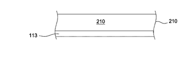
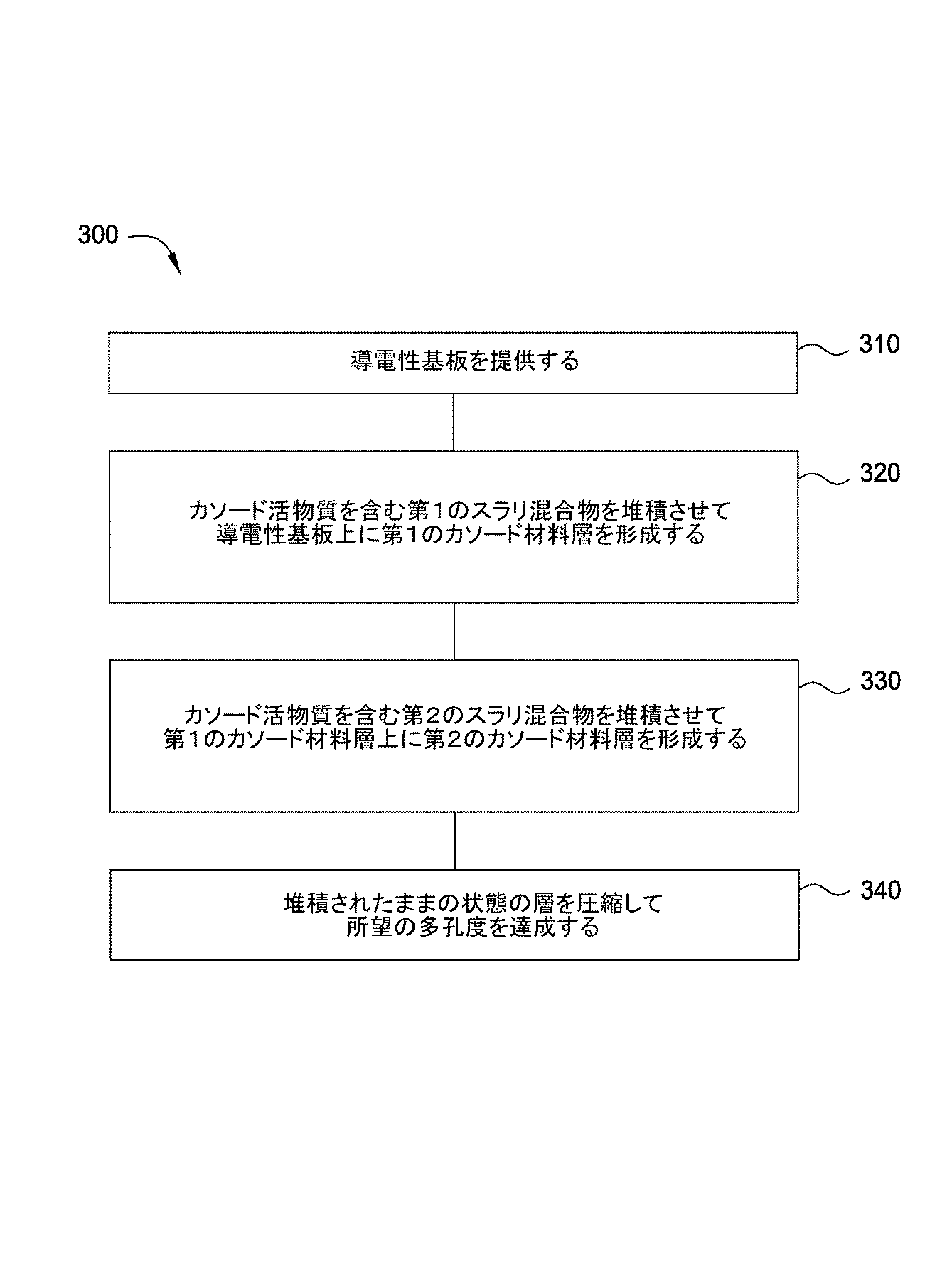
図2A〜2Cは、本明細書に記載の実施形態に従って形成される部分多層カソード電極構造体103の一実施形態の概略横断面図である。図3は、本明細書に記載の実施形態に従って多層カソード電極構造体を形成するための方法の一実施形態を要約する処理フローチャート300である。図2A〜2Cの多層電極構造体103が処理フローチャート300を参照して論じられる。
2A-2C are schematic cross-sectional views of one embodiment of a partial multilayer
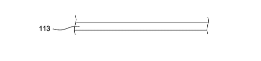
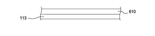
ブロック310で、導電性基板が提供される。導電性基板は集電体113と同様であってよい。図2Aに描くように、集電体113が、集電体113への多層カソード材料202の堆積に先立って概略的に例示される。一実施形態では、集電体113は導電性基板(たとえば、金属箔、シート、または板)である。一実施形態では、集電体113はフレキシブル導電性基板(たとえば、金属箔)である。一実施形態では、集電体113は絶縁被覆がその上に設けられる導電性基板である。一実施形態では、集電体113は、金属やプラスチック、黒鉛、ポリマー、炭素含有ポリマー、複合材、他の適切な材料などの1つまたは複数の導電性材料を含むホスト基板上に設けられる比較的薄い導電層を含んでよい。集電体113が構成されてよい金属の例には、アルミニウム(Al)、銅(Cu)、亜鉛(Zn)、ニッケル(Ni)、コバルト(Co)、スズ(Sn)、マンガン(Mn)、マグネシウム(Mg)、それらの合金、およびそれらの組合せがある。一実施形態では、集電体113は穿孔される。
At
あるいは集電体113は、物理的気相堆積(PVD)、電気化学メッキ、無電解メッキなどを含み、当該技術分野で公知の手段によりその上に形成される導電層を有するガラスや、シリコン、プラスチックまたはポリマー基板などの非導電性であるホスト基板を備えてよい。一実施形態では、集電体113はフレキシブルホスト基板から形成される。フレキシブルホスト基板は、導電層がその上に形成される、ポリエチレンや、ポリプロピレン、他の適切なプラスチックまたはポリマー材料などの軽量で安価なプラスチック材料であってよい。一実施形態では、導電層は、抵抗損失を最小限にするために、厚さが約10と15ミクロンの間である。そのようなフレキシブル基板としての使用に適する材料には、ポリイミド(たとえば、DuPont CorporationによるKAPTON(商標))、ポリエチレンテレフタレート(PET)、ポリアクリレート、ポリカーボネート、シリコン、エポキシ樹脂、シリコン官能化エポキシ樹脂、ポリエステル(たとえば、E.I.du Pont de Nemours&Co.によるMYLAR(商標))、Kanegaftigi Chemical Industry Company製APICAL AV、宇部興産株式会社製UPILEX、住友製ポリエーテルスルホン(PES)、ポリエーテルイミド(たとえば、General Electric CompanyによるULTEM)、およびポリエチレンナフタレン(PEN)がある。代わりに、フレキシブル基板はポリマー被覆で補強される比較的薄いガラスから構成されてよい。
Alternatively, the
一実施形態では、集電体113は、集電体113に対する電極の接触抵抗および接着を向上させるために、多層カソード材料202の形成に先立って処理される。
In one embodiment, the
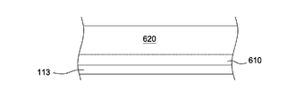
ブロック320で、カソード活物質を含む第1のスラリ混合物が集電体113に堆積されて、図2Bに示すように集電体113上に第1のカソード材料層210を形成する。一実施形態では、第1のカソード材料層210は約10μm〜約150μmの間の厚さを有する。一実施形態では、第1のカソード材料層210は約50μm〜約100μmの間の厚さを有する。集電体113が多孔性構造体である実施形態では、第1のカソード材料層210は集電体113の細孔内に堆積されてよい。
At
第1のスラリ混合物は、次の堆積技法のうちのいずれかを用いて基板上に堆積されてよい:スプレー堆積法、スライドコーティング法、カーテンコーティング法、スリットコーティング法、流動層コーティング法、パターン化ロールコーティング法(たとえば、巻線やローレット、グラビア)を含むロールコーティング法、浸漬コーティング、印刷法(たとえば、リソグラフィや押出印刷)、およびドクターブレード法。スプレー堆積法には、液圧スプレー法、空気圧スプレー法、噴霧スプレー法、エレクトロスプレー法、静電スプレー法、プラズマスプレー法、および熱または火炎スプレー法があるが、これらに限定されない。 The first slurry mixture may be deposited on the substrate using any of the following deposition techniques: spray deposition, slide coating, curtain coating, slit coating, fluidized bed coating, patterning. Roll coating methods including roll coating methods (eg winding, knurling, gravure), dip coating, printing methods (eg lithography or extrusion printing), and doctor blade methods. Spray deposition methods include, but are not limited to, hydraulic spray methods, pneumatic spray methods, spray spray methods, electrospray methods, electrostatic spray methods, plasma spray methods, and thermal or flame spray methods.
第1のスラリ混合物は、カソード活物質、ならびにバインダ、導電性材料および溶媒のうちの少なくとも1つを含んでよい。 The first slurry mixture may include a cathode active material and at least one of a binder, a conductive material, and a solvent.
例証的なカソード活物質には、コバルト酸リチウム(LiCoO2)、二酸化マンガンリチウム(LiMnO2)、二硫化チタン(TiS2)、LiNixCo1−2xMnxO2(「NMC」)、LiMn2O4、鉄オリビン(LiFePO4)およびそのバリアント(LiFe1−xMgxPO4など)、LiMoPO4、LiCoPO4、Li3V2(PO4)3、LiVOPO4、LiMP2O7、LiFe1.5P2O7、LiVPO4F、LiAlPO4F、Li5V(PO4)2F2、Li5Cr(PO4)2F2、Li2CoPO4F、Li2NiPO4F、Na5V2(PO4)2F3、Li2FeSiO4、Li2MnSiO4、Li2VOSiO4、それらの複合材、ならびにそれらの組合せがある。 Illustrative cathode active materials include lithium cobaltate (LiCoO 2 ), lithium manganese dioxide (LiMnO 2 ), titanium disulfide (TiS 2 ), LiNi x Co 1-2x Mn x O 2 (“NMC”), LiMn 2 O 4 , iron olivine (LiFePO 4 ) and variants thereof (such as LiFe 1-x Mg x PO 4 ), LiMoPO 4 , LiCoPO 4 , Li 3 V 2 (PO 4 ) 3 , LiVOPO 4 , LiMP 2 O 7 , LiFe 1.5 P 2 O 7 , LiVPO 4 F, LiAlPO 4 F, Li 5 V (PO 4 ) 2 F 2 , Li 5 Cr (PO 4 ) 2 F 2 , Li 2 CoPO 4 F, Li 2 NiPO 4 F, Na 5 V 2 (PO 4 ) 2 F 3 , Li 2 FeSiO 4 , Li 2 MnSiO 4 , Li 2 VOSiO 4 and their composites, as well as combinations thereof.
第1のスラリ混合物はカソード活物質を約30重量%と約96重量%との間で含んでよい。第1のスラリ混合物はカソード活物質を約75重量%と約96重量%との間で含んでよい。第1のスラリ混合物はカソード活物質を約85重量%と約92重量%との間で含んでよい。第1のスラリ混合物は固形物を約50〜80重量%の間で含み、その固形物の約75〜98重量%がカソード活物質であってよい。スラリ混合物は固形物を約55〜65重量%の間で含み、その固形物の約85〜95重量%がカソード活物質であってよい。 The first slurry mixture may comprise between about 30% and about 96% by weight of the cathode active material. The first slurry mixture may include between about 75% and about 96% by weight of the cathode active material. The first slurry mixture may comprise between about 85% and about 92% by weight of the cathode active material. The first slurry mixture may comprise between about 50-80 wt% solids, and about 75-98 wt% of the solids may be the cathode active material. The slurry mixture may comprise between about 55-65% by weight of solids and about 85-95% by weight of the solids may be the cathode active material.
一実施形態では、カソード活物質は粒子の形態にある。一実施形態では、粒子はナノスケール粒子である。一実施形態では、ナノスケール粒子は約1nmと約100nmとの間の直径を有する。一実施形態では、粒子はマイクロスケール粒子である。一実施形態では、粒子は凝集マイクロスケール粒子を含む。一実施形態では、マイクロスケール粒子は約1μmと約20μmとの間の直径を有する。一実施形態では、マイクロスケール粒子は、約2μmと約15μmとの間の直径を有する。特定の実施形態では、より高電圧で起こりかねない不要な副反応を回避するために低減された表面積を維持しながら、粒子の充填密度を維持する粒径を選択することが望ましい。特定の実施形態では、粒径は使用されるカソード活物質の種類に依存してよい。 In one embodiment, the cathode active material is in the form of particles. In one embodiment, the particles are nanoscale particles. In one embodiment, the nanoscale particles have a diameter between about 1 nm and about 100 nm. In one embodiment, the particles are microscale particles. In one embodiment, the particles comprise agglomerated microscale particles. In one embodiment, the microscale particles have a diameter between about 1 μm and about 20 μm. In one embodiment, the microscale particles have a diameter between about 2 μm and about 15 μm. In certain embodiments, it is desirable to select a particle size that maintains the packing density of the particles while maintaining a reduced surface area to avoid unwanted side reactions that may occur at higher voltages. In certain embodiments, the particle size may depend on the type of cathode active material used.
第1のスラリ混合物は、固体結合剤または固体結合剤を形成するための前駆体をさらに含んでよい。結合剤は、カソード活物質の基板とのおよびカソード活物質の他の粒子との結合を容易にする。結合剤は典型的にポリマーである。結合剤は溶媒に可溶であってよい。結合剤は水溶性結合剤であってよい。結合剤は有機溶媒に可溶であってよい。例証的な結合剤には、スチレンブタジエンゴム(SBR)、カルボキシメチルセルロース(CMC)、ポリフッ化ビニリデン(PVDF)、およびそれらの組合せがある。固体結合剤は、集電体113への堆積に先立ってカソード活物質と混合されてよい。固体結合剤は、カソード活物質の堆積前か後かどちらかで集電体に堆積されてよい。固体結合剤は、カソード活物質を集電体113の表面に保持するために、ポリマーなどのバインダを含んでよい。結合剤は一般に、堆積層の性能を低下させることを回避するためにいくらかの電気またはイオン伝導度を有するであろうが、しかしながら、たいていの結合剤は通常は電気的に絶縁しており、いくつかの材料はリチウムイオンの通過を許可しない。特定の実施形態では、結合剤は低分子量を有するポリマーを含有する炭素である。低分子量ポリマーは、集電体113へのカソード活物質の接着を促進するために約10,000よりも小さい数平均分子量を有してよい。
The first slurry mixture may further comprise a solid binder or a precursor for forming the solid binder. The binder facilitates bonding of the cathode active material with the substrate and with other particles of the cathode active material. The binder is typically a polymer. The binder may be soluble in the solvent. The binder may be a water soluble binder. The binder may be soluble in an organic solvent. Illustrative binders include styrene butadiene rubber (SBR), carboxymethyl cellulose (CMC), polyvinylidene fluoride (PVDF), and combinations thereof. The solid binder may be mixed with the cathode active material prior to deposition on the
第1のスラリ混合物は結合剤を約0.5重量%と約15重量%との間で含んでよい。スラリ混合物は結合剤を約1重量%と約4重量%との間で含んでよい。第1のスラリ混合物は固形物を約50〜80重量%の間で含み、その固形物が結合剤の約1〜10重量%を含んでよい。スラリ混合物は固形物を約55〜65重量%の間で含み、その固形物が結合剤の約1〜4重量%を含んでよい。 The first slurry mixture may include between about 0.5 wt% and about 15 wt% binder. The slurry mixture may comprise between about 1% and about 4% by weight binder. The first slurry mixture may comprise between about 50-80% by weight solids, and the solids may comprise about 1-10% by weight of the binder. The slurry mixture may comprise between about 55-65% by weight of solids, which solids may comprise about 1-4% by weight of the binder.
第1のスラリ混合物は、カソード活物質の高抵抗粒子間の導電経路を提供するための導電性材料をさらに含んでよい。一実施形態では、導電性材料は、黒鉛、グラフェン硬質炭素、アセチレンブラック(AB)、カーボンブラック(CB)、炭素被覆シリコン、スズ粒子、酸化スズ、炭化ケイ素、シリコン(アモルファスまたは結晶性)、シリコン合金、ドープされたシリコン、チタン酸リチウム、それらの複合材、およびそれらの組合せからなる群から選択されてよい。 The first slurry mixture may further include a conductive material for providing a conductive path between the high resistance particles of the cathode active material. In one embodiment, the conductive material is graphite, graphene hard carbon, acetylene black (AB), carbon black (CB), carbon-coated silicon, tin particles, tin oxide, silicon carbide, silicon (amorphous or crystalline), silicon It may be selected from the group consisting of alloys, doped silicon, lithium titanate, composites thereof, and combinations thereof.
第1のスラリ混合物は導電性材料を約2重量%と約10重量%との間で含んでよい。スラリ混合物は導電性材料を約4重量%と約8重量%との間で含んでよい。第1のスラリ混合物は固形物を約50〜80重量%の間で含み、その固形物が導電性材料の約1〜20重量%を含んでよい。スラリ混合物は固形物を約55〜65重量%の間で含み、その固形物が導電性材料の約2〜10重量%を含んでよい。 The first slurry mixture may include between about 2% and about 10% by weight of conductive material. The slurry mixture may comprise between about 4% and about 8% by weight of conductive material. The first slurry mixture may comprise between about 50-80% by weight solids, and the solids may comprise about 1-20% by weight of the conductive material. The slurry mixture may comprise between about 55-65% by weight of solids, and the solids may comprise about 2-10% by weight of the conductive material.
例証的な溶媒にはN−メチルピロリドン(NMP)および水がある。 Exemplary solvents include N-methylpyrrolidone (NMP) and water.
第1のスラリ混合物は固形物を約50〜80重量%の間、および溶媒を約20〜50重量%含んでよい。第1のスラリ混合物は固形物を約55〜65重量%の間、および溶媒を約35〜45重量%含んでよい。 The first slurry mixture may comprise between about 50-80% solids and about 20-50% solvent by weight. The first slurry mixture may comprise between about 55-65% by weight solids and about 35-45% by weight solvent.
特定の実施形態では、第1のスラリ混合物は高固形物量の材料を有する。第1のスラリ混合物は、第1のスラリ混合物の全重量パーセントに基づいて30重量%よりも大きい、40重量%よりも大きい、50重量%よりも大きい、60重量%よりも大きい、70重量%よりも大きい、80重量%よりも大きい、または90重量%よりも大きい高固形物量を有してよい。第1のスラリ混合物は、第1のスラリ混合物の全重量パーセントに基づいて30重量%〜95重量%の範囲の高固形物量を有してよい。第1のスラリ混合物は、第1のスラリ混合物の全重量パーセントに基づいて40重量%〜85重量%の範囲の高固形物量を有してよい。第1のスラリ混合物は、第1のスラリ混合物の全重量パーセントに基づいて50重量%〜70重量%の範囲の高固形物量を有してよい。第1のスラリ混合物は、第1のスラリ混合物の全重量パーセントに基づいて65重量%〜70重量%の範囲の高固形物量を有してよい。 In certain embodiments, the first slurry mixture has a high solids material. The first slurry mixture is greater than 30 wt%, greater than 40 wt%, greater than 50 wt%, greater than 60 wt%, 70 wt% based on the total weight percent of the first slurry mixture May have a high solids amount greater than, greater than 80 wt%, or greater than 90 wt%. The first slurry mixture may have a high solids content in the range of 30 wt% to 95 wt% based on the total weight percent of the first slurry mixture. The first slurry mixture may have a high solids content ranging from 40% to 85% by weight based on the total weight percent of the first slurry mixture. The first slurry mixture may have a high solids content in the range of 50 wt% to 70 wt% based on the total weight percent of the first slurry mixture. The first slurry mixture may have a high solids content in the range of 65 wt% to 70 wt% based on the total weight percent of the first slurry mixture.
任意選択でブロック320の後または間に、第1のスラリ混合物は、スラリ混合物に存在する液体、たとえば溶媒を除去するために任意選択の乾燥処理に曝露されてよい。第1のスラリ混合物は、堆積処理からすべての残っている溶媒を除去するために任意選択の乾燥処理に曝露されてよい。任意選択の乾燥処理は、たとえばスラリ混合物を加熱ガス(たとえば、加熱窒素)に曝露する空気乾燥処理、真空乾燥処理、赤外線乾燥処理、およびスラリ混合物が堆積される集電体を加熱することなどの乾燥処理を含んでよいが、これに限定されない。
Optionally, after or during
特定の実施形態では、第1のスラリ混合物は、材料の堆積の間に任意選択の乾燥処理に曝露されてよい。たとえば、第1のスラリ混合物が基板上に堆積される間、導電性基板/集電体113が加熱されてよい。同時の加熱と材料の堆積の例は、2012年2月22日出願のBolandiらに対する「LITHIUM ION CELL DESIGN APPRATUS AND METHOD」という名称の、本発明の譲受人に譲渡された米国特許出願公開第2012/0219841号に開示されている。基板は摂氏約80度から摂氏約180度までの温度に加熱されてよい。
In certain embodiments, the first slurry mixture may be exposed to an optional drying process during material deposition. For example, the conductive substrate /
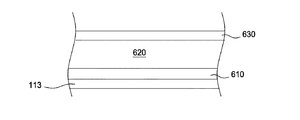
ブロック330で、カソード活物質を含む第2のスラリ混合物が第1のカソード材料層210に堆積されて、第2のカソード材料層220を形成する。第2のスラリ混合物は本明細書に記載のような第1のスラリ混合物と同様であってよい。第1のスラリ混合物を参照して上述したように、第2のスラリ混合物は、カソード活物質、ならびにバインダ、導電性材料および溶媒のうちの少なくとも1つを含んでよい。
At
特定の実施形態では、第2のスラリ混合物と第1のスラリ混合物は液体/固形物量(たとえば、溶媒/カソード材料)が異なる。スラリ混合物の液体量が異なる特定の実施形態では、液体の蒸発が、第1のカソード材料層210と第2のカソード材料層220との間の多孔度の差をもたらす。たとえば、第1のスラリ混合物は約1−0.25と約0.33−0.25との間の液固(質量)比を有してよく、第2のスラリ混合物は約1−0.25と約1−0.33との間の液固比を有してよい。たとえば、第1のスラリ混合物は約1:0.25と約0.33:0.25との間の液固(質量)比を有してよく、第2のスラリ混合物は約1:0.25と約1:0.33との間の液固比を有してよい。
In certain embodiments, the second slurry mixture and the first slurry mixture have different liquid / solid amounts (eg, solvent / cathode material). In certain embodiments where the amount of liquid in the slurry mixture is different, the evaporation of the liquid results in a difference in porosity between the first
特定の実施形態では、第1のカソード材料層210は60重量%よりも大きい固形物量を有してよく、第2のカソード材料層220は約50〜60重量%の間の固形物量を有してよい。特定の実施形態では、第2のカソード材料層220は60重量%よりも大きい固形物量を有してよく、第1のカソード材料層210は約50〜60重量%の間の固形物量を有してよい。
In certain embodiments, the first
第2のスラリ混合物は固形物を約50重量%と約80重量%との間で含んでよい。第2のスラリ混合物は固形物を約55重量%と約65重量%との間で含んでよい。第2のスラリ混合物の固形物はカソード活物質を約75重量%と約98重量%との間で含んでよい。第2のスラリ混合物の固形物はカソード活物質を約85重量%と約95重量%との間で含んでよい。第2のスラリ混合物の固形物は結合剤を約1重量%と約10重量%との間で含んでよい。第2のスラリ混合物の固形物は結合剤を約1重量%と約4重量%との間で含んでよい。第2のスラリ混合物の固形物は導電性材料を約1重量%と約20重量%との間で含んでよい。第2のスラリ混合物の固形物は導電性材料を約2重量%と約10重量%との間で含んでよい。第2のスラリ混合物は溶媒を約20重量%と約50重量%との間で含んでよい。第2のスラリ混合物は溶媒を約35重量%と約45重量%との間で含んでよい。 The second slurry mixture may comprise between about 50 wt% and about 80 wt% solids. The second slurry mixture may comprise between about 55% and about 65% by weight solids. The solids of the second slurry mixture may include between about 75% and about 98% by weight of the cathode active material. The solids of the second slurry mixture may include between about 85% and about 95% by weight of the cathode active material. The solids of the second slurry mixture may contain between about 1% and about 10% by weight binder. The solids of the second slurry mixture may include between about 1% and about 4% by weight binder. The solids of the second slurry mixture may include between about 1% and about 20% by weight of conductive material. The solids of the second slurry mixture may include between about 2% and about 10% by weight conductive material. The second slurry mixture may comprise between about 20% and about 50% by weight of solvent. The second slurry mixture may comprise between about 35% and about 45% by weight of solvent.
任意選択でブロック330の後に、第2のスラリ混合物は、スラリ混合物に存在する液体、たとえば溶媒を除去するために任意選択の乾燥処理に曝露されてよい。第2のスラリ混合物は、堆積処理からすべての残っている溶媒を除去するために任意選択の乾燥処理に曝露されてよい。任意選択の乾燥処理は、たとえばスラリ混合物を加熱ガス(たとえば、加熱窒素)の少なくとも1つに曝露する空気乾燥処理、真空乾燥処理、赤外線乾燥処理、およびスラリ混合物が堆積される集電体を加熱することなどの乾燥処理を含んでよいが、これに限定されない。特定の実施形態では、第1のスラリ混合物と第2のスラリ混合物との両方が同時に乾燥されてよい。
Optionally, after
特定の実施形態では、第2のスラリ混合物は、材料の堆積の間に任意選択の乾燥処理に曝露されてよい。たとえば、第2のスラリ混合物が基板上に堆積される間、導電性基板/集電体113と堆積された第1のスラリ混合物または第1のカソード材料層210が加熱されてよい。基板は摂氏約80度から摂氏約180度までの温度に加熱されてよい。
In certain embodiments, the second slurry mixture may be exposed to an optional drying process during material deposition. For example, the conductive substrate /
乾燥後、第1のカソード材料層210は約40と約75との間の多孔度を有してよい。特定の実施形態では、第1のカソード材料層210の多孔度は、第2のカソード材料層220の多孔度よりも大きい。特定の実施形態では、第1のカソード材料層210は少なくとも40%または45%の多孔度を有する。特定の実施形態では、第1のカソード材料層210は45%または50%までの多孔度を有する。一実施形態では、第1のカソード材料層210の多孔度は、同じ材料から形成される固体膜と比較して約40%と約50%との間であり、第2のカソード材料層220の多孔度は、同じ材料から形成される固体膜と比較して約30%と約35%との間である。
After drying, the first
ブロック340で、堆積されたままの状態の第1のカソード材料層210と第2のカソード材料層220は圧縮されて、所望の多孔度を達成する。いくつかの実施形態では、約2,000〜7,000psiの圧力が圧縮処理の間カソード材料層に印加される。導電性基板上に堆積されたカソード材料層は、層の表面を平坦化しながら圧密粒子の所望の正味密度を達成するために、圧縮技法、たとえば、カレンダ処理を用いて圧縮されてよい。
At
特定の実施形態では、圧縮後の第1のカソード材料層210は第2のカソード材料層220の多孔度よりも大きい多孔度を有する。特定の実施形態では、第1のカソード材料層210は少なくとも15%の多孔度を有する。特定の実施形態では、第1のカソード材料層210は35%までの多孔度を有する。特定の実施形態では、第1のカソード材料層210の多孔度は、同じ材料から形成される固体膜と比較して約15%と約35%との間であり、第2のカソード材料層220の多孔度は、同じ材料から形成される固体膜と比較して約30%と約55%との間である。特定の実施形態では、第1のカソード材料層210の多孔度は、同じ材料から形成される固体膜と比較して約18%と約27%との間であり、第2のカソード材料層220の多孔度は、同じ材料から形成される固体膜と比較して約37%と約50%との間である。
In certain embodiments, the compressed first
特定の実施形態では、第1のカソード材料層210の多孔度は第2のカソード材料層220の多孔度よりも小さい。特定の実施形態では、第2のカソード材料層220の多孔度は、同じ材料から形成される固体膜と比較して約15%と約35%との間であり、第1のカソード材料層210の多孔度は、同じ材料から形成される固体膜と比較して約30%と約55%との間である。特定の実施形態では、第2のカソード材料層220の多孔度は、同じ材料から形成される固体膜と比較して約18%と約27%との間であり、第1のカソード材料層210の多孔度は、同じ材料から形成される固体膜と比較して約37%と約50%との間である。
In certain embodiments, the porosity of the first
特定の実施形態では、第1のカソード材料層210のカソード活物質と第2のカソード材料層220のカソード活物質は同一の材料である。特定の実施形態では、第1のカソード材料層210のカソード活物質と第2のカソード材料層220のカソード活物質は、各層の性質を異ならせるように選択される異なる材料である。各層に異なるカソード活物質が使用される特定の実施形態では、カソード活物質は、単一の圧縮処理を用いて各個々の層で所望の密度/多孔度を達成するために、粒子のより容易な充填を可能にする異なる粒径を有する。
In a specific embodiment, the cathode active material of the first
特定の実施形態では、第1の層210のカソード活物質の平均粒径と第2の層220のカソード活物質の平均粒径は同様である。特定の実施形態では、第1の層210のカソード活物質の平均粒径と第2の層220のカソード活物質の平均粒径は異なる。特定の実施形態では、第1のカソード材料層210のカソード活物質と第2のカソード材料層220のカソード活物質は異なる粒径の同じ材料を含む。平均粒径の差は各層の異なる表面積および/または異なる多孔度をもたらす。
In certain embodiments, the average particle size of the cathode active material of the
特定の実施形態では、活物質の各層のために、存在する活物質の他層に対して異なるモード粒径分布(たとえば、単モードや、双モード、多モード)が使用されてよい。各層での異なるモード粒径分布の利用は、単一の圧縮処理を用いて各個々の層で所望の密度/多孔度を達成するために、粒子のより容易な充填を可能にする。たとえば特定の実施形態では、第1のカソード材料層210は単モード粒径分布を有し、第2のカソード材料層220は双モード粒径分布を有する。特定の実施形態では、第1のカソード材料層210は双モードまたは多モード粒径分布を有し、第2のカソード材料層220は単モード粒径分布を有する。単モードおよび双モード粒径のための例示的な平均粒子直径には3ミクロン、6ミクロン、および10ミクロンがある。
In certain embodiments, a different modal particle size distribution (eg, single mode, bimode, multimode) may be used for each layer of active material relative to other layers of active material present. The use of different modal particle size distributions in each layer allows easier packing of particles to achieve the desired density / porosity in each individual layer using a single compression process. For example, in certain embodiments, the first
特定の実施形態では、第1のスラリ混合物と第2スラリ混合物は同じ堆積技法を用いて堆積される。たとえば、第1のスラリ混合物と第2のスラリ混合物はドクターブレード法またはエレクトロスプレー法を用いて堆積されてよい。特定の実施形態では、第1のスラリ混合物と第2のスラリ混合物は異なる堆積技術を用いて堆積されてよい。たとえば、第1のスラリ混合物はドクターブレード法を用いて堆積されてよく、第2のスラリ混合物はエレクトロスプレー法を用いて堆積されてよい。 In certain embodiments, the first slurry mixture and the second slurry mixture are deposited using the same deposition technique. For example, the first slurry mixture and the second slurry mixture may be deposited using a doctor blade method or an electrospray method. In certain embodiments, the first slurry mixture and the second slurry mixture may be deposited using different deposition techniques. For example, the first slurry mixture may be deposited using a doctor blade method and the second slurry mixture may be deposited using an electrospray method.
特定の実施形態では、多層カソード電極において、各層は他層のカソード活物質のタップ密度と異なるタップ密度を有するカソード活物質を含む。特定の実施形態では、第1のカソード材料層210は約2g/cm3と約3g/cm3との間のタップ密度を有するカソード活物質を含む。特定の実施形態では、第2のカソード材料層220は約2g/cm3と約3g/cm3との間のタップ密度を有する材料を含む。特定の実施形態では、第1のカソード材料層210は約3μmの平均粒径と約2.5g/cm3のタップ密度を有するカソード活物質を含み、第2のカソード材料層220は約10μmの平均粒径と約2.8g/cm3のタップ密度を有するカソード活物質を含む。特定の実施形態では、第1のカソード材料層210は約10ミクロンの平均粒径と約2.8g/cm3のタップ密度を有するカソード活物質を含み、第2のカソード材料層220は約3ミクロンの平均粒径と約2.5g/cm3のタップ密度を有するカソード活物質を含む。典型的に、より小さい粒子は材料のグラム当たりより高い表面積を有し、したがって、より高い多孔度を有すると予期される。より高いタップ密度が低多孔度を生み出すと考えられる。
In a specific embodiment, in the multilayer cathode electrode, each layer includes a cathode active material having a tap density different from the tap density of the cathode active material of the other layer. In certain embodiments, the first
例示的構造体
(A)一実施形態では、カソード構造体103の第1のカソード材料層210は、超低電極多孔度(たとえば、15〜20%多孔度)を達成するために高充填密度を有する「エネルギー層」である。第1のカソード材料層210は約8ミクロン〜約25ミクロンの平均粒径を有するLiCoO2を含む。第1のカソード材料層210は約1〜80ミクロンの平均厚さを有してよい。第2のカソード材料層220は「電力層」であり、約30%〜約60%の多孔度を有する。第2のカソード材料層220は約1〜約6ミクロンの粒径を有するNMC、LiFePO4、またはLiMn2O4を含んでよい。第2のカソード材料層220は約10〜80ミクロンの厚さを有してよい。いくつかの実施形態では、第2のカソード材料層220に対する第1のカソード材料層210の厚さ比は約5:1〜1:5の間である。
Exemplary Structure (A) In one embodiment, the first
(B)一実施形態では、(A)と同様のカソード材料を2と20層の間で含有する多層電極構造体が設けられる。多層電極構造体は2と20層の間を含有し、約50〜200ミクロンの全電極厚さを有してよい。多層電極構造体は段階的多孔度を有してよい。たとえば一実施形態では、多層電極構造体の層は、カソード材料の密度が集電体113に隣接して最大であり(たとえば、第1のカソード材料層210)、カソード材料の密度が各層の堆積とともに減少するように堆積されてよい。いくつかの実施形態では、多層電極構造体の層は、カソード材料の密度が集電体113に隣接して最小であり(たとえば、第1のカソード材料層210)、カソード材料の密度が各層の堆積とともに増加するように堆積されてよい。 (B) In one embodiment, a multilayer electrode structure is provided that contains between 2 and 20 cathode materials similar to (A). The multilayer electrode structure may contain between 2 and 20 layers and have a total electrode thickness of about 50-200 microns. The multilayer electrode structure may have a graded porosity. For example, in one embodiment, the layers of the multilayer electrode structure have the highest cathode material density adjacent to current collector 113 (eg, first cathode material layer 210), and the cathode material density is the deposition of each layer. It may be deposited to decrease with time. In some embodiments, the layers of the multilayer electrode structure have a minimum cathode material density adjacent to the current collector 113 (eg, the first cathode material layer 210) and the cathode material density of each layer. It may be deposited so as to increase with deposition.
(C)特定の実施形態において、以下のようにパートAの多層電極構造体が堆積されてよい:第1のカソード材料層210はエレクトロスプレー処理に続いてカレンダ処理を用いて堆積されてよく、第2のカソード材料層220はスロットダイ処理を用いて堆積されてよい。いくつかの実施形態では、第2のカソード材料層220はカレンダ加工されてもよい。
(C) In certain embodiments, the multilayer electrode structure of Part A may be deposited as follows: the first
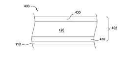
図4A〜4Dは、本明細書に記載の実施形態に従って形成される部分多層カソード電極構造体403の別の実施形態の概略横断面図である。図5は、本明細書に記載の実施形態に従って多層カソード電極構造体を形成するための方法の一実施形態を要約する処理フローチャート500である。図4A〜4Dの多層電極構造体103が処理フローチャート500を参照して論じられる。
4A-4D are schematic cross-sectional views of another embodiment of a partial multi-layer
ブロック510で、導電性基板が提供される。フローチャート300のブロック310を参照して上述したように、導電性基板は集電体113と同様であってよい。図4Aに描くように、集電体113が、集電体113への多層カソード材料402の堆積に先立って概略的に例示される。
At
ブロック520で、第1のバインダリッチ層410が導電性基板上に形成される。第1のバインダリッチ層410は、第1のカソード材料層が集電体113に接着するのに役立つ。第1のバインダリッチ層410は、本明細書に記載の堆積技法のうちのいずれかを用いてスラリ混合物を堆積させることにより形成されてよい。第1のバインダリッチ層410を形成するためのスラリ混合物は、上述の第1のカソード材料層210と第2のカソード材料層220を堆積させるための、本明細書に記載のスラリ混合物と同様であってよい。第1のバインダリッチ層410を形成するためのスラリ混合物は、カソード活物質、バインダ、および導電性材料と溶剤のうちの少なくとも1つを含んでよい。第1のバインダリッチ層410は典型的にバインダを4.2重量%よりも多く含む。
At
一実施形態では、第1のバインダリッチ層410は約30μm〜約100μmの間の厚さを有する。一実施形態では、第1のバインダリッチ層410は約40μm〜約65μmの間の厚さを有する。第1のバインダリッチ層410は、同じ材料から形成される固体膜と比較して約15%と約35%との間の多孔度を有してよい。第1のバインダリッチ層410は、同じ材料から形成される固体膜と比較して約18%と約27%との間の多孔度を有してよい。
In one embodiment, the first binder
ブロック530で、カソード活物質を含むスラリ混合物がバインダリッチ層410上に堆積されて、第1のカソード材料層420を形成する。第1のカソード材料層420は、上述の第1のカソード材料層210または第2のカソード材料層220のうちのどちらかと同様であってよい。第1のカソード材料層420は、本明細書に記載の堆積技法のうちのいずれかを用いてスラリ混合物を堆積させることにより形成されてよい。第1のカソード材料層420を形成するためのスラリ混合物は、上述の第1のカソード材料層210と第2のカソード材料層220を堆積させるための、本明細書に記載のスラリ混合物と同様であってよい。
At
特定の実施形態では、第1のバインダリッチ層410と第1のカソード材料層420は同じ堆積層から形成されてよい。たとえば、単層がスラリ混合物を用いて集電体113に堆積されてよく、バインダは堆積されたままの状態の単層の底部に向かって沈殿することとなり、単層の底部にバインダリッチ部分を形成する。
In certain embodiments, the first binder
一実施形態では、第1のカソード材料層420は約30μm〜約100μmの間の厚さを有する。一実施形態では、第1のカソード材料層420は約40μm〜約65μmの間の厚さを有する。第1のカソード材料層420は、同じ材料から形成される固体膜と比較して約15%と約35%との間の多孔度を有してよい。第1のカソード材料層420は、同じ材料から形成される固体膜と比較して約18%と約27%との間の多孔度を有してよい。
In one embodiment, the first
ブロック540で、第2のバインダリッチ層430が第1のカソード材料層420上に形成される。第2のバインダリッチ層430は、本明細書に記載の堆積技法のうちのいずれかを用いてスラリ混合物を堆積させることにより形成されてよい。第2のバインダリッチ層430を形成するためのスラリ混合物は、上述の第1の層210と第2の層220を堆積させるための、本明細書に記載のスラリ混合物と同様であってよい。第1のバインダリッチ層410を形成するためのスラリ混合物と同様に、第2のバインダリッチ層430を形成するためのスラリ混合物は、カソード活物質、バインダ、および導電性材料と溶剤のうちの少なくとも1つを含んでよい。第1のバインダリッチ層420を形成するためのスラリ混合物は典型的に、バインダを4.2重量%よりも多く含む。
At
一実施形態では、第2のバインダリッチ層430は約30μm〜約100μmの間の厚さを有する。一実施形態では、第2のバインダリッチ層430は約60μm〜約80μmの間の厚さを有する。第2のバインダリッチ層430は、同じ材料から形成される固体膜と比較して約30%と約55%との間の多孔度を有してよい。第2のバインダリッチ層430は、同じ材料から形成される固体膜と比較して約35%と約50%との間の多孔度を有してよい。
In one embodiment, the second binder
任意選択でブロック520、530および540のうちのいずれかの後に、スラリ混合物は、スラリ混合物に存在する液体、たとえば溶媒を除去するために任意選択の乾燥処理に曝露されてよい。第2のスラリ混合物は、堆積処理からすべての残っている溶媒を除去するために任意選択の乾燥処理に曝露されてよい。任意選択の乾燥処理は、たとえばスラリ混合物を加熱ガス(たとえば、加熱窒素)の少なくとも1つに曝露する空気乾燥処理、真空乾燥処理、赤外線乾燥処理、およびスラリ混合物が堆積される集電体を加熱することなどの乾燥処理を含んでよいが、これに限定されない。特定の実施形態では、スラリ混合物は同時に乾燥されてよい。
Optionally, after any of
ブロック550で、堆積されたままの状態の第1のバインダリッチ層410、カソード材料層420、および第2のバインダリッチ層430は圧縮されて、所望の多孔度を達成する。粒子が導電性基板上に堆積された後、粒子は、層の表面を平坦化しながら圧密粒子の所望の正味密度を達成するために、圧縮技法、たとえば、カレンダ処理を用いて圧縮されてよい。いくつかの実施形態では、約2,000〜7,000psiの圧力が圧縮処理の間カソード材料層に印加される。
At
特定の実施形態では、圧縮後の第1のカソード材料層420は少なくとも15%の多孔度を有する。特定の実施形態では、第1のカソード材料層420は35%までの多孔度を有する。特定の実施形態では、第1のカソード材料層420の多孔度は、同じ材料から形成される固体膜と比較して約15%と約35%との間であり、第2の層の多孔度は、同じ材料から形成される固体膜と比較して約30%と約55%との間である。特定の実施形態では、第1のカソード材料層420の多孔度は、同じ材料から形成される固体膜と比較して約18%と約27%との間であり、第2の層の多孔度は、同じ材料から形成される固体膜と比較して約37%と約50%との間である。
In certain embodiments, the compressed first
図6A〜6Fは、本明細書に記載の実施形態に従って形成される部分多層カソード電極構造体603の一実施形態の概略横断面図である。図7は、本明細書に記載の実施形態に従って多層カソード電極構造体を形成するための方法の一実施形態を要約する処理フローチャート700である。図6A〜6Fの多層電極構造体103が処理フローチャート700を参照して論じられる。
6A-6F are schematic cross-sectional views of one embodiment of a partial multilayer
ブロック710で、導電性基板が提供される。フローチャート300のブロック310を参照して上述したように、導電性基板は集電体113と同様であってよい。図6Aに描くように、集電体113が、集電体113への多層カソード材料604の堆積に先立って概略的に例示される。
At
ブロック720で、第1のバインダリッチ層610が導電性基板上に形成される。第1のバインダリッチ層610は、本明細書に記載の堆積技法のうちのいずれかを用いてスラリ混合物を堆積させることにより形成されてよい。第1のバインダリッチ層610を形成するためのスラリ混合物は、上述の第1のバインダリッチ層410、第1のカソード材料層210および第2のカソード材料層220を堆積させるための、本明細書に記載のスラリ混合物と同様であってよい。第1のバインダリッチ層610を形成するためのスラリ混合物は、カソード活物質、バインダ、および導電性材料と溶剤のうちの少なくとも1つを含んでよい。第1のバインダリッチ層610を形成するためのスラリ混合物は典型的に、バインダを4.2重量%よりも多く含む。
At
一実施形態では、第1のバインダリッチ層610は約30μm〜約100μmの間の厚さを有する。一実施形態では、第1のバインダリッチ層610は約40μm〜約65μmの間の厚さを有する。第1のバインダリッチ層610は、同じ材料から形成される固体膜と比較して約15%と約35%との間の多孔度を有してよい。第1のバインダリッチ層610は、同じ材料から形成される固体膜と比較して約18%と約27%との間の多孔度を有してよい。
In one embodiment, the first binder
ブロック730で、カソード活物質を含む第1のスラリ混合物が第1のバインダリッチ層610上に堆積されて、第1のバインダリッチ層610に第1のカソード材料層620を形成する。第1のカソード材料層620は、上述の第1のカソード材料層210または第2のカソード材料層220のうちのどちらかと同様であってよい。第1のカソード材料層620は、本明細書に記載の堆積技法のうちのいずれかを用いてスラリ混合物を堆積させることにより形成されてよい。第1のカソード材料層620を形成するためのスラリ混合物は、上述の第1のカソード材料層210と第2のカソード材料層220を堆積させるための、本明細書に記載のスラリ混合物と同様であってよい。
At
第1のバインダリッチ層410と第1のカソード材料層420を参照して上述したように、第1のバインダリッチ層610と第1のカソード材料層620は同じ堆積層から形成されてよい。
As described above with reference to the first binder-
一実施形態では、第1のカソード材料層620は約30μm〜約100μmの間の厚さを有する。一実施形態では、第1のカソード材料層620は約40μm〜約65μmの間の厚さを有する。第1のカソード材料層620は、同じ材料から形成される固体膜と比較して約15%と約35%との間の多孔度を有してよい。第1のカソード材料層620は、同じ材料から形成される固体膜と比較して約18%と約27%との間の多孔度を有してよい。
In one embodiment, the first
ブロック740で、第2のバインダリッチ層630が第1のカソード材料層620上に形成される。第2のバインダリッチ層630は安定性を提供し、第1のカソード材料層620と第2のカソード材料層640との間の層間剥離を防止するのに役立つ。第2のバインダリッチ層630は、本明細書に記載の堆積技法のうちのいずれかを用いてスラリ混合物を堆積させることにより形成されてよい。第2のバインダリッチ層630を形成するためのスラリ混合物は、上述の第1のカソード材料層210と第2のカソード材料層220を堆積させるための、本明細書に記載のスラリ混合物と同様であってよい。第1のバインダリッチ層610を形成するためのスラリ混合物と同様に、第2のバインダリッチ層630を形成するためのスラリ混合物は、カソード活物質、バインダ、および導電性材料と溶剤のうちの少なくとも1つを含んでよい。第2のバインダリッチ層630は典型的に、バインダを4.2重量%よりも多く含む。
At
一実施形態では、第2のバインダリッチ層630は約30μm〜約100μmの間の厚さを有する。一実施形態では、第2のバインダリッチ層630は約40μm〜約65μmの間の厚さを有する。第2のバインダリッチ層630は、同じ材料から形成される固体膜と比較して約15%と約35%との間の多孔度を有してよい。第2のバインダリッチ層630は、同じ材料から形成される固体膜と比較して約18%と約27%との間の多孔度を有してよい。
In one embodiment, the second binder
ブロック750で、第2のスラリ混合物が第2のバインダリッチ層630上に堆積されて、第2のバインダリッチ層630上に第2のカソード材料層640を形成する。第2のカソード材料層640は、本明細書に記載の堆積技法のうちのいずれかを用いてスラリ混合物を堆積させることにより形成されてよい。第2のスラリ混合物は上述の第1のスラリ混合物と同様であってよい。第1のスラリ混合物を参照して上述したように、第2のスラリ混合物は、カソード活物質、ならびにバインダ、導電性材料および溶媒のうちの少なくとも1つを含んでよい。
At
一実施形態では、第2のカソード材料層640は約30μm〜約100μmの間の厚さを有する。一実施形態では、第2のカソード材料層640は約40μm〜約65μmの間の厚さを有する。第2のカソード材料層640は、同じ材料から形成される固体膜と比較して約15%と約35%との間の多孔度を有してよい。第2のカソード材料層640は、同じ材料から形成される固体膜と比較して約18%と約27%との間の多孔度を有してよい。
In one embodiment, the second
特定の実施形態では、第1のカソード材料層210は、以下のうちのいずれかで第2のカソード材料層220と異なってよい:層間で異なる多孔度をもたらす各層で異なるスラリ組成物、各層で異なる活物質、層間で異なる表面積および/または異なる多孔度をもたらす各層で同じ活物質の異なる粒径、層間で異なる粒径分布(たとえば、単モード、双モード、多モード)、各層で異なる電極組成物(バインダ、導電性添加物、活物質)、および異なるタップ密度。
In certain embodiments, the first
ブロック760で、第3のバインダリッチ層650が第2のカソード材料層640上に形成される。第3のバインダリッチ層650は、本明細書に記載の堆積技法のうちのいずれかを用いてスラリ混合物を堆積させることにより形成されてよい。第3のバインダリッチ層650を形成するためのスラリ混合物は、上述の第1のカソード材料層210と第2のカソード材料層220を堆積させるための、本明細書に記載のスラリ混合物と同様であってよい。第1のバインダリッチ層610を形成するためのスラリ混合物と同様に、第3のバインダリッチ層650を形成するためのスラリ混合物は、カソード活物質、バインダ、および導電性材料と溶剤のうちの少なくとも1つを含んでよい。第3のバインダリッチ層650を形成するためのスラリ混合物は典型的に、バインダを4.2重量%よりも多く含む。
At
一実施形態では、第3のバインダリッチ層650は約30μm〜約100μmの間の厚さを有する。一実施形態では、第3のバインダリッチ層650は約40μm〜約65μmの間の厚さを有する。第3のバインダリッチ層650は、同じ材料から形成される固体膜と比較して約15%と約35%との間の多孔度を有してよい。第3のバインダリッチ層650は、同じ材料から形成される固体膜と比較して約18%と約27%との間の多孔度を有してよい。
In one embodiment, the third binder
任意選択でブロック720、730、740、750,760、および770のうちのいずれかの後に、スラリ混合物は、スラリ混合物に存在する液体、たとえば溶媒を除去するために任意選択の乾燥処理に曝露されてよい。第2のスラリ混合物は、堆積処理からすべての残っている溶媒を除去するために任意選択の乾燥処理に曝露されてよい。任意選択の乾燥処理は、たとえばスラリ混合物を加熱ガス(たとえば、加熱窒素)の少なくとも1つに曝露する空気乾燥処理、真空乾燥処理、赤外線乾燥処理、およびスラリ混合物が堆積される集電体を加熱することなどの乾燥処理を含んでよいが、これに限定されない。特定の実施形態では、両スラリ混合物は同時に乾燥されてよい。
Optionally, after any of
ブロック770で、第1のバインダリッチ層610、第1のカソード材料層620、第2のバインダリッチ層630、第2のカソード材料層640および第3のバインダリッチ層650は圧縮されて、所望の多孔度を達成する。粒子が導電性基板上に堆積された後、粒子は、層の表面を平坦化しながら圧密粒子の所望の正味密度を達成するために、圧縮技法、たとえば、カレンダ処理を用いて圧縮されてよい。いくつかの実施形態では、約2,000〜7,000psiの圧力が圧縮処理の間カソード材料層に印加される。
At
特定の実施形態では、圧縮後の第1のカソード材料層620は第2のカソード材料層640の多孔度よりも大きい多孔度を有する。特定の実施形態では、圧縮後、第1のカソード材料層620の多孔度は第2のカソード材料層640の多孔度よりも小さい。
In certain embodiments, the compressed first
本明細書に記載の実施形態をさらに例示するために、以下の非限定的な実施例が提供される。しかしながら実施例は、包括的であるものとは意図されず、本明細書に記載の実施形態の範囲を限定するものとは意図されない。 The following non-limiting examples are provided to further illustrate the embodiments described herein. However, the examples are not intended to be exhaustive and are not intended to limit the scope of the embodiments described herein.
固形分65重量%を有し、PVDF4重量%、カーボンブラック(CB)3.2重量%、およびニッケルマンガンコバルト酸リチウム(NMC)92.8重量%を含む第1および第2のスラリ組成物が以下の実施例に使用された。MX−3標識NMCは3ミクロンの平均粒径を有し、MX−10標識NMCは10ミクロンの平均粒径を有した。両スラリ組成物はNMCをカソード活物質として含有した。 First and second slurry compositions having a solids content of 65 wt%, comprising 4 wt% PVDF, 3.2 wt% carbon black (CB), and 92.8 wt% lithium nickel manganese cobaltate (NMC) Used in the following examples. MX-3 labeled NMC had an average particle size of 3 microns and MX-10 labeled NMC had an average particle size of 10 microns. Both slurry compositions contained NMC as the cathode active material.
実施例B0507−1〜B0507−3
実施例B0507−1〜B0507−3に関して、MX−10を有する第1のスラリ混合物がドクターブレード処理を用いて18.5ミクロンの厚さを有するアルミニウム箔集電体上に堆積された。アルミニウム箔集電体および第1のスラリ混合物は、溶媒を蒸発させて第1のカソード材料層を形成するために、摂氏80度に加熱された。MX−3を有する第2のスラリ混合物が第1のカソード材料層上に堆積された。アルミニウム箔集電体、第1のカソード材料層および第2のスラリ混合物は、溶媒を蒸発させて第2のカソード材料層を形成するために、摂氏80度に加熱された。第1のカソード材料層および第2のカソード材料層は2,000と7,000psiの間の圧力で単一のカレンダ処理に曝露された。第1のカソード材料層は65.8ミクロンの最終厚さと36%の最終多孔度を有した。第2のカソード材料層は97.6ミクロンの最終厚さと42%の最終多孔度を有した。
Example B0507-1 to B0507-3
For Examples B0507-1 to B0507-3, a first slurry mixture having MX-10 was deposited on an aluminum foil current collector having a thickness of 18.5 microns using a doctor blade process. The aluminum foil current collector and the first slurry mixture were heated to 80 degrees Celsius to evaporate the solvent and form the first cathode material layer. A second slurry mixture having MX-3 was deposited on the first cathode material layer. The aluminum foil current collector, the first cathode material layer, and the second slurry mixture were heated to 80 degrees Celsius to evaporate the solvent and form the second cathode material layer. The first cathode material layer and the second cathode material layer were exposed to a single calendar process at a pressure between 2,000 and 7,000 psi. The first cathode material layer had a final thickness of 65.8 microns and a final porosity of 36%. The second cathode material layer had a final thickness of 97.6 microns and a final porosity of 42%.
実施例B0508−1〜B0508−3
実施例B0508−1〜B0508−3に関して、MX−3を有する第1のスラリ混合物がドクターブレード処理を用いて18.8ミクロンの厚さを有するアルミニウム箔集電体上に堆積された。アルミニウム箔集電体および第1のスラリ混合物は、溶媒を蒸発させて第1のカソード材料層を形成するために、摂氏80度に加熱された。MX−10を有する第2のスラリ混合物が第1のカソード材料層上に堆積された。アルミニウム箔集電体、第1のカソード材料層および第2のスラリ混合物は、溶媒を蒸発させて第2のカソード材料層を形成するために、摂氏80度に加熱された。第1のカソード材料層および第2のカソード材料層は2,000と7,000psiの間の圧力で単一のカレンダ処理に曝露された。第1のカソード材料層は64.6ミクロンの最終厚さと38%の最終多孔度を有した。第2のカソード材料層は110ミクロンの最終厚さと34%の最終多孔度を有した。
Example B0508-1 to B0508-3
For Examples B0508-1 through B0508-3, a first slurry mixture having MX-3 was deposited on an aluminum foil current collector having a thickness of 18.8 microns using a doctor blade process. The aluminum foil current collector and the first slurry mixture were heated to 80 degrees Celsius to evaporate the solvent and form the first cathode material layer. A second slurry mixture having MX-10 was deposited on the first cathode material layer. The aluminum foil current collector, the first cathode material layer, and the second slurry mixture were heated to 80 degrees Celsius to evaporate the solvent and form the second cathode material layer. The first cathode material layer and the second cathode material layer were exposed to a single calendar process at a pressure between 2,000 and 7,000 psi. The first cathode material layer had a final thickness of 64.6 microns and a final porosity of 38%. The second cathode material layer had a final thickness of 110 microns and a final porosity of 34%.
結果 表1
上記は本発明の実施形態を対象とするが、本発明の他のさらなる実施形態がその基本的な範囲から逸脱することなく考案でき、その範囲は以下特許請求の範囲により定められる。 While the foregoing is directed to embodiments of the present invention, other and further embodiments of the invention can be devised without departing from the basic scope thereof, which is defined by the following claims.
Claims (15)
カソード活物質を含む第1のスラリ混合物を堆積させて前記導電性基板上に第1のカソード材料層を形成することと、
カソード活物質を含む第2のスラリ混合物を堆積させて前記第1のカソード材料層上に第2のカソード材料層を形成することと、
堆積されたままの状態の前記第1のカソード材料層と前記第2のカソード材料層を圧縮して所望の多孔度を達成することとを含む、多層カソード構造体を形成するための方法。 Providing a conductive substrate;
Depositing a first slurry mixture comprising a cathode active material to form a first cathode material layer on the conductive substrate;
Depositing a second slurry mixture comprising a cathode active material to form a second cathode material layer on the first cathode material layer;
A method for forming a multi-layer cathode structure comprising compressing the first cathode material layer and the second cathode material layer as deposited to achieve a desired porosity.
カソード活物質と、
結合剤、結合前駆体、導電性材料および溶媒のうちの少なくとも1つとを含む、請求項1に記載の方法。 Each of the first slurry mixture and the second slurry mixture independently;
A cathode active material;
The method of claim 1, comprising at least one of a binder, a bond precursor, a conductive material, and a solvent.
Applications Claiming Priority (3)
| Application Number | Priority Date | Filing Date | Title |
|---|---|---|---|
| US201361790684P | 2013-03-15 | 2013-03-15 | |
| US61/790,684 | 2013-03-15 | ||
| PCT/US2014/020788 WO2014149766A1 (en) | 2013-03-15 | 2014-03-05 | Multi-layer battery electrode design for enabling thicker electrode fabrication |
Publications (1)
| Publication Number | Publication Date |
|---|---|
| JP2016510941A true JP2016510941A (en) | 2016-04-11 |
Family
ID=51580652
Family Applications (1)
| Application Number | Title | Priority Date | Filing Date |
|---|---|---|---|
| JP2016500667A Pending JP2016510941A (en) | 2013-03-15 | 2014-03-05 | Multi-layer battery electrode design to enable thicker electrode manufacturing |
Country Status (6)
| Country | Link |
|---|---|
| US (1) | US20160013480A1 (en) |
| JP (1) | JP2016510941A (en) |
| KR (1) | KR20150132463A (en) |
| CN (1) | CN105074967B (en) |
| TW (1) | TWI616017B (en) |
| WO (1) | WO2014149766A1 (en) |
Cited By (3)
| Publication number | Priority date | Publication date | Assignee | Title |
|---|---|---|---|---|
| JP2019501492A (en) * | 2016-06-14 | 2019-01-17 | エルジー・ケム・リミテッド | Secondary battery electrode and lithium secondary battery including the same |
| JP2022500838A (en) * | 2019-04-04 | 2022-01-04 | エルジー・ケム・リミテッド | Electrode for lithium secondary battery |
| JP2022100395A (en) * | 2018-11-13 | 2022-07-05 | ビークルエナジージャパン株式会社 | Lithium ion secondary battery and method for manufacturing the same |
Families Citing this family (53)
| Publication number | Priority date | Publication date | Assignee | Title |
|---|---|---|---|---|
| JP6032160B2 (en) * | 2013-09-02 | 2016-11-24 | トヨタ自動車株式会社 | Method for manufacturing electrode of secondary battery by ESD method |
| US9711784B2 (en) | 2014-05-01 | 2017-07-18 | Sion Power Corporation | Electrode fabrication methods and associated systems and articles |
| JP2016181487A (en) * | 2015-03-25 | 2016-10-13 | 株式会社東芝 | Electrode for nonaqueous electrolyte battery, nonaqueous electrolyte secondary battery, and battery pack |
| KR101810185B1 (en) * | 2015-04-29 | 2017-12-19 | 주식회사 엘지화학 | An electrode for an electrochemical device and a method for manufacturing the same |
| CN105098193A (en) * | 2015-09-24 | 2015-11-25 | 宁德时代新能源科技有限公司 | Positive plate and lithium ion battery comprising same |
| WO2017077055A1 (en) * | 2015-11-04 | 2017-05-11 | Basf Se | Layer composite and electrode having a smooth surface |
| KR102645603B1 (en) * | 2016-01-22 | 2024-03-07 | 더 리전트 오브 더 유니버시티 오브 캘리포니아 | high-voltage device |
| KR102133383B1 (en) * | 2016-03-03 | 2020-07-14 | 주식회사 엘지화학 | Method for manufacturing positive electrode for lithium secondary battery and positive electrode for lithium secondary battery manufactured thereby |
| KR101919048B1 (en) * | 2016-06-27 | 2019-02-08 | 주식회사 네패스 | Manufacturing method of anode for lithium secondary battery |
| KR20180001518A (en) * | 2016-06-27 | 2018-01-04 | 주식회사 네패스 | Composition for lithium secondary battery anode, manufacturing method of lithium secondary battery anode using the same, lithium secondary battery anode and lithium secondary battery made therefrom |
| DE102016215542A1 (en) | 2016-08-18 | 2018-02-22 | Robert Bosch Gmbh | Electrode for a battery cell, method for producing an electrode and battery cell |
| US10847780B2 (en) * | 2016-09-16 | 2020-11-24 | Pacesetter, Inc. | Battery electrode and methods of making |
| KR20180049986A (en) * | 2016-11-04 | 2018-05-14 | 삼성에스디아이 주식회사 | Positive electrode for rechargeable lithium battery and rechargeable lithium battery including same |
| TWI617073B (en) * | 2016-11-25 | 2018-03-01 | 財團法人工業技術研究院 | Battery electrode structure and method for fabricating the same |
| US20180261827A1 (en) * | 2017-03-08 | 2018-09-13 | Ricoh Company, Ltd. | Electrode, electrode element, nonaqueous electrolytic power storage device |
| JP7065451B2 (en) * | 2017-05-30 | 2022-05-12 | パナソニックIpマネジメント株式会社 | Positive electrode for secondary battery and secondary battery |
| US10038193B1 (en) | 2017-07-28 | 2018-07-31 | EnPower, Inc. | Electrode having an interphase structure |
| CN110574194B (en) * | 2017-11-06 | 2022-06-03 | 株式会社Lg化学 | Spinel-structured lithium manganese-based positive electrode active material, and positive electrode and lithium secondary battery comprising same |
| US20190198934A1 (en) * | 2017-12-21 | 2019-06-27 | GM Global Technology Operations LLC | Method of generating silicon thick electrodes with improved life performance |
| CN110010900A (en) * | 2018-01-04 | 2019-07-12 | 中国科学院苏州纳米技术与纳米仿生研究所 | A kind of high magnification thick electrode and the preparation method and application thereof |
| CN109004175B (en) * | 2018-02-26 | 2020-09-18 | 宁德新能源科技有限公司 | Positive pole piece and lithium ion battery |
| CN113299876B (en) * | 2018-02-26 | 2023-03-10 | 宁德新能源科技有限公司 | Pole piece and lithium ion battery |
| US20190296335A1 (en) | 2018-03-23 | 2019-09-26 | EnPower, Inc. | Electrochemical cells having improved ionic conductivity |
| US11245106B2 (en) * | 2018-04-12 | 2022-02-08 | Samsung Sdi Co., Ltd. | Electrode assembly and rechargeable battery including same |
| JP7079411B2 (en) * | 2018-04-24 | 2022-06-02 | トヨタ自動車株式会社 | Electrodes and batteries using them |
| CN113764616A (en) * | 2018-08-28 | 2021-12-07 | 宁德新能源科技有限公司 | Pole piece and electrochemical device |
| CN109301160B (en) * | 2018-09-05 | 2022-03-04 | 上海奥威科技开发有限公司 | Electrode, preparation method thereof and lithium ion capacitor battery |
| CN112956052A (en) * | 2018-09-06 | 2021-06-11 | 新罗纳米技术有限公司 | Electrode with conductive intermediate layer and method thereof |
| CN113675367B (en) * | 2018-11-05 | 2023-08-25 | 宁德新能源科技有限公司 | Positive electrode sheet, electrochemical device and electronic device comprising same |
| CN113544874A (en) * | 2018-11-15 | 2021-10-22 | 美商映能量公司 | Layered electrode with high speed top layer |
| KR102304738B1 (en) * | 2018-11-30 | 2021-09-24 | 주식회사 엘지화학 | Method for preparing positive electrode active material precursor for lithium secondary battery |
| CN109560249A (en) * | 2018-11-30 | 2019-04-02 | 中国科学院过程工程研究所 | A kind of double-layer structure anode pole piece, and its preparation method and application |
| US11569550B2 (en) | 2019-04-05 | 2023-01-31 | EnPower, Inc. | Electrode with integrated ceramic separator |
| CN110474019B (en) * | 2019-07-08 | 2020-10-30 | 广州中国科学院工业技术研究院 | High-specific energy battery positive pole piece and preparation method thereof |
| CN112652734A (en) * | 2019-10-11 | 2021-04-13 | 广州汽车集团股份有限公司 | Thick negative pole piece and preparation method thereof, lithium ion battery cell, lithium ion battery pack and application thereof |
| US10998553B1 (en) | 2019-10-31 | 2021-05-04 | EnPower, Inc. | Electrochemical cell with integrated ceramic separator |
| EP4062467A1 (en) * | 2019-11-21 | 2022-09-28 | Volkswagen Aktiengesellschaft | Dry electrode manufacturing |
| EP4060760A4 (en) * | 2019-12-20 | 2023-01-11 | LG Energy Solution, Ltd. | Positive electrode for lithium secondary battery, and lithium secondary battery comprising same |
| CN111211325B (en) * | 2020-03-09 | 2021-09-17 | 广东工业大学 | Lithium ion battery cathode material and preparation method and application thereof |
| CN111342029B (en) * | 2020-03-20 | 2021-10-22 | 浙江中金格派锂电产业股份有限公司 | Preparation method of composite anode of lithium ion battery |
| WO2021189481A1 (en) * | 2020-03-27 | 2021-09-30 | 宁德新能源科技有限公司 | Positive electrode piece and electrochemical apparatus comprising same, and electronic apparatus |
| KR20220054954A (en) * | 2020-10-26 | 2022-05-03 | 에스케이온 주식회사 | Multi-layered electrode for battery and fabrication method thereof |
| CN112467075B (en) * | 2020-11-05 | 2022-01-04 | 东莞塔菲尔新能源科技有限公司 | Pole piece, electric core and secondary battery |
| CN115485879A (en) * | 2021-01-29 | 2022-12-16 | 株式会社Lg新能源 | Positive electrode and lithium secondary battery comprising same |
| EP3998654A1 (en) * | 2021-02-19 | 2022-05-18 | Lilium eAircraft GmbH | Hybrid electrode |
| WO2022270799A1 (en) * | 2021-06-24 | 2022-12-29 | 주식회사 엘지에너지솔루션 | Cathode for secondary lithium battery and secondary lithium battery comprising same |
| US11594784B2 (en) | 2021-07-28 | 2023-02-28 | EnPower, Inc. | Integrated fibrous separator |
| CN115911247B (en) * | 2021-09-30 | 2024-03-22 | 宁德时代新能源科技股份有限公司 | Positive electrode plate, secondary battery, battery module, battery pack and electricity utilization device |
| CN114335418B (en) * | 2021-12-23 | 2024-04-02 | 惠州亿纬锂能股份有限公司 | Positive electrode plate and preparation method and application thereof |
| CN116417579A (en) * | 2021-12-29 | 2023-07-11 | 宁德时代新能源科技股份有限公司 | Positive electrode active material, method for producing positive electrode material, positive electrode sheet, secondary battery, battery module, battery pack, and electricity-using device |
| KR20230159947A (en) * | 2022-05-16 | 2023-11-23 | 에스케이온 주식회사 | Electrode for secondary battery, manufucturing method thereof, and lithium secondary battary |
| WO2024091625A1 (en) * | 2022-10-26 | 2024-05-02 | Texpower, Inc. | Low-cobalt or cobalt-free cathode materials with bimodal particle size distribution for lithium batteries |
| TWI821118B (en) * | 2023-02-14 | 2023-11-01 | 台灣立凱電能科技股份有限公司 | High-voltage composite positive electrode material and manufacturing method thereof |
Citations (3)
| Publication number | Priority date | Publication date | Assignee | Title |
|---|---|---|---|---|
| US20110168550A1 (en) * | 2010-01-13 | 2011-07-14 | Applied Materials, Inc. | Graded electrode technologies for high energy lithium-ion batteries |
| US20120219841A1 (en) * | 2011-02-25 | 2012-08-30 | Applied Materials, Inc. | Lithium ion cell design apparatus and method |
| US20130017340A1 (en) * | 2011-07-12 | 2013-01-17 | Applied Materials, Inc. | Methods to fabricate variations in porosity of lithium ion battery electrode films |
Family Cites Families (9)
| Publication number | Priority date | Publication date | Assignee | Title |
|---|---|---|---|---|
| DE60140163D1 (en) * | 2000-08-28 | 2009-11-26 | Nissan Motor | Rechargeable lithium ion battery |
| EP1978587B1 (en) * | 2007-03-27 | 2011-06-22 | Hitachi Vehicle Energy, Ltd. | Lithium secondary battery |
| JP2009004289A (en) * | 2007-06-25 | 2009-01-08 | Panasonic Corp | Nonaqueous electrolyte secondary battery |
| CN102388498B (en) * | 2009-04-10 | 2014-04-23 | 丰田自动车株式会社 | Lithium ion battery and utilization thereof |
| US20120328942A1 (en) * | 2010-03-05 | 2012-12-27 | A123 Systems, Inc. | Design and fabrication of electrodes with gradients |
| EP2586084A2 (en) * | 2010-06-22 | 2013-05-01 | K2 Energy Solutions, Inc. | Lithium ion battery |
| JP2013543221A (en) * | 2010-09-30 | 2013-11-28 | エルジー・ケム・リミテッド | Positive electrode for lithium secondary battery and lithium secondary battery including the same |
| JP5519586B2 (en) * | 2011-06-29 | 2014-06-11 | 株式会社日立製作所 | ELECTRODE FOR LITHIUM ION SECONDARY BATTERY AND ITS MANUFACTURING METHOD, LITHIUM ION SECONDARY BATTERY AND ITS MANUFACTURING METHOD |
| CN102324493B (en) * | 2011-08-26 | 2016-03-30 | 东莞新能源科技有限公司 | There is thick electrode of good electrical chemical property and preparation method thereof |
-
2014
- 2014-03-05 CN CN201480010713.4A patent/CN105074967B/en not_active Expired - Fee Related
- 2014-03-05 US US14/771,126 patent/US20160013480A1/en not_active Abandoned
- 2014-03-05 JP JP2016500667A patent/JP2016510941A/en active Pending
- 2014-03-05 WO PCT/US2014/020788 patent/WO2014149766A1/en active Application Filing
- 2014-03-05 KR KR1020157029495A patent/KR20150132463A/en not_active Application Discontinuation
- 2014-03-13 TW TW103109114A patent/TWI616017B/en not_active IP Right Cessation
Patent Citations (3)
| Publication number | Priority date | Publication date | Assignee | Title |
|---|---|---|---|---|
| US20110168550A1 (en) * | 2010-01-13 | 2011-07-14 | Applied Materials, Inc. | Graded electrode technologies for high energy lithium-ion batteries |
| US20120219841A1 (en) * | 2011-02-25 | 2012-08-30 | Applied Materials, Inc. | Lithium ion cell design apparatus and method |
| US20130017340A1 (en) * | 2011-07-12 | 2013-01-17 | Applied Materials, Inc. | Methods to fabricate variations in porosity of lithium ion battery electrode films |
Cited By (5)
| Publication number | Priority date | Publication date | Assignee | Title |
|---|---|---|---|---|
| JP2019501492A (en) * | 2016-06-14 | 2019-01-17 | エルジー・ケム・リミテッド | Secondary battery electrode and lithium secondary battery including the same |
| JP2022010000A (en) * | 2016-06-14 | 2022-01-14 | エルジー・ケム・リミテッド | Electrode for secondary battery and lithium secondary battery including the same |
| JP2022100395A (en) * | 2018-11-13 | 2022-07-05 | ビークルエナジージャパン株式会社 | Lithium ion secondary battery and method for manufacturing the same |
| JP2022500838A (en) * | 2019-04-04 | 2022-01-04 | エルジー・ケム・リミテッド | Electrode for lithium secondary battery |
| JP7177277B2 (en) | 2019-04-04 | 2022-11-22 | エルジー エナジー ソリューション リミテッド | Electrodes for lithium secondary batteries |
Also Published As
| Publication number | Publication date |
|---|---|
| TWI616017B (en) | 2018-02-21 |
| US20160013480A1 (en) | 2016-01-14 |
| CN105074967B (en) | 2018-07-10 |
| KR20150132463A (en) | 2015-11-25 |
| TW201442324A (en) | 2014-11-01 |
| CN105074967A (en) | 2015-11-18 |
| WO2014149766A1 (en) | 2014-09-25 |
Similar Documents
| Publication | Publication Date | Title |
|---|---|---|
| TWI616017B (en) | Multi-layer battery electrode design for enabling thicker electrode fabrication | |
| TWI689128B (en) | Interphase layer for improved lithium metal cycling | |
| JP6367390B2 (en) | Production of large capacity prism lithium ion alloy anode | |
| US20200259180A1 (en) | Prelithiated multilayer dry electrode and methods | |
| TWI518972B (en) | Graded electrode technologies for high energy lithium-ion batteries | |
| KR20160002988A (en) | Electrochemical cell with solid and liquid electrolytes | |
| US11271196B2 (en) | Electrochemical cells having improved ionic conductivity | |
| TW201737534A (en) | Anode structure with binders for silicon and stabilized lithium metal powder | |
| JP5832729B2 (en) | Secondary battery electrode and non-aqueous electrolyte battery | |
| JP2016510939A (en) | Electrode surface roughness control for spray coating process of lithium ion battery | |
| CN112928277A (en) | Anode-free all-solid-state battery | |
| US20220045366A1 (en) | Method for production of laminated solid electrolyte-based components and electrochemical cells using same | |
| KR20160027364A (en) | Electrode assembly for secondary battery | |
| US20210013498A1 (en) | Electrochemical cells having improved ionic conductivity | |
| CN111386616A (en) | Method of manufacturing electrode for secondary battery and method of manufacturing secondary battery | |
| US11349125B2 (en) | Spacer included electrodes structure and its application for high energy density and fast chargeable lithium ion batteries | |
| EP3186847A1 (en) | Carbon nanotube-based lithium ion battery | |
| JP6926910B2 (en) | Rechargeable battery | |
| US10790505B2 (en) | Electrochemical cells having improved ionic conductivity | |
| JP2019220356A (en) | Positive electrode material for lithium ion secondary battery, method for manufacturing the same and positive electrode active substance layer containing the same, and lithium ion secondary battery arranged by use thereof | |
| JP7359491B2 (en) | Battery and its manufacturing method | |
| JP6832474B2 (en) | Positive electrode material for lithium ion secondary battery, positive electrode active material layer, and lithium ion secondary battery | |
| WO2022208625A1 (en) | Power storage device electrode and lithium ion secondary battery | |
| KR20230009460A (en) | Battery and its manufacturing method | |
| JP2023545832A (en) | Advanced lithium-ion energy storage device |
Legal Events
| Date | Code | Title | Description |
|---|---|---|---|
| A621 | Written request for application examination |
Free format text: JAPANESE INTERMEDIATE CODE: A621 Effective date: 20170201 |
|
| A977 | Report on retrieval |
Free format text: JAPANESE INTERMEDIATE CODE: A971007 Effective date: 20171220 |
|
| A131 | Notification of reasons for refusal |
Free format text: JAPANESE INTERMEDIATE CODE: A131 Effective date: 20180109 |
|
| A521 | Request for written amendment filed |
Free format text: JAPANESE INTERMEDIATE CODE: A523 Effective date: 20180406 |
|
| A131 | Notification of reasons for refusal |
Free format text: JAPANESE INTERMEDIATE CODE: A131 Effective date: 20180703 |
|
| A02 | Decision of refusal |
Free format text: JAPANESE INTERMEDIATE CODE: A02 Effective date: 20190226 |