JP2015171226A - inverter device and air conditioner - Google Patents
inverter device and air conditioner Download PDFInfo
- Publication number
- JP2015171226A JP2015171226A JP2014044286A JP2014044286A JP2015171226A JP 2015171226 A JP2015171226 A JP 2015171226A JP 2014044286 A JP2014044286 A JP 2014044286A JP 2014044286 A JP2014044286 A JP 2014044286A JP 2015171226 A JP2015171226 A JP 2015171226A
- Authority
- JP
- Japan
- Prior art keywords
- inverter device
- gate
- voltage line
- inverter
- gate voltage
- Prior art date
- Legal status (The legal status is an assumption and is not a legal conclusion. Google has not performed a legal analysis and makes no representation as to the accuracy of the status listed.)
- Pending
Links
Images


Classifications
-
- H—ELECTRICITY
- H03—ELECTRONIC CIRCUITRY
- H03K—PULSE TECHNIQUE
- H03K17/00—Electronic switching or gating, i.e. not by contact-making and –breaking
- H03K17/04—Modifications for accelerating switching
- H03K17/0406—Modifications for accelerating switching in composite switches
-
- H—ELECTRICITY
- H02—GENERATION; CONVERSION OR DISTRIBUTION OF ELECTRIC POWER
- H02M—APPARATUS FOR CONVERSION BETWEEN AC AND AC, BETWEEN AC AND DC, OR BETWEEN DC AND DC, AND FOR USE WITH MAINS OR SIMILAR POWER SUPPLY SYSTEMS; CONVERSION OF DC OR AC INPUT POWER INTO SURGE OUTPUT POWER; CONTROL OR REGULATION THEREOF
- H02M1/00—Details of apparatus for conversion
- H02M1/42—Circuits or arrangements for compensating for or adjusting power factor in converters or inverters
- H02M1/4208—Arrangements for improving power factor of AC input
- H02M1/4225—Arrangements for improving power factor of AC input using a non-isolated boost converter
-
- H—ELECTRICITY
- H02—GENERATION; CONVERSION OR DISTRIBUTION OF ELECTRIC POWER
- H02M—APPARATUS FOR CONVERSION BETWEEN AC AND AC, BETWEEN AC AND DC, OR BETWEEN DC AND DC, AND FOR USE WITH MAINS OR SIMILAR POWER SUPPLY SYSTEMS; CONVERSION OF DC OR AC INPUT POWER INTO SURGE OUTPUT POWER; CONTROL OR REGULATION THEREOF
- H02M3/00—Conversion of dc power input into dc power output
- H02M3/22—Conversion of dc power input into dc power output with intermediate conversion into ac
- H02M3/24—Conversion of dc power input into dc power output with intermediate conversion into ac by static converters
- H02M3/28—Conversion of dc power input into dc power output with intermediate conversion into ac by static converters using discharge tubes with control electrode or semiconductor devices with control electrode to produce the intermediate ac
- H02M3/325—Conversion of dc power input into dc power output with intermediate conversion into ac by static converters using discharge tubes with control electrode or semiconductor devices with control electrode to produce the intermediate ac using devices of a triode or a transistor type requiring continuous application of a control signal
- H02M3/335—Conversion of dc power input into dc power output with intermediate conversion into ac by static converters using discharge tubes with control electrode or semiconductor devices with control electrode to produce the intermediate ac using devices of a triode or a transistor type requiring continuous application of a control signal using semiconductor devices only
-
- H—ELECTRICITY
- H02—GENERATION; CONVERSION OR DISTRIBUTION OF ELECTRIC POWER
- H02M—APPARATUS FOR CONVERSION BETWEEN AC AND AC, BETWEEN AC AND DC, OR BETWEEN DC AND DC, AND FOR USE WITH MAINS OR SIMILAR POWER SUPPLY SYSTEMS; CONVERSION OF DC OR AC INPUT POWER INTO SURGE OUTPUT POWER; CONTROL OR REGULATION THEREOF
- H02M5/00—Conversion of ac power input into ac power output, e.g. for change of voltage, for change of frequency, for change of number of phases
- H02M5/40—Conversion of ac power input into ac power output, e.g. for change of voltage, for change of frequency, for change of number of phases with intermediate conversion into dc
- H02M5/42—Conversion of ac power input into ac power output, e.g. for change of voltage, for change of frequency, for change of number of phases with intermediate conversion into dc by static converters
- H02M5/44—Conversion of ac power input into ac power output, e.g. for change of voltage, for change of frequency, for change of number of phases with intermediate conversion into dc by static converters using discharge tubes or semiconductor devices to convert the intermediate dc into ac
- H02M5/453—Conversion of ac power input into ac power output, e.g. for change of voltage, for change of frequency, for change of number of phases with intermediate conversion into dc by static converters using discharge tubes or semiconductor devices to convert the intermediate dc into ac using devices of a triode or transistor type requiring continuous application of a control signal
- H02M5/458—Conversion of ac power input into ac power output, e.g. for change of voltage, for change of frequency, for change of number of phases with intermediate conversion into dc by static converters using discharge tubes or semiconductor devices to convert the intermediate dc into ac using devices of a triode or transistor type requiring continuous application of a control signal using semiconductor devices only
-
- H—ELECTRICITY
- H03—ELECTRONIC CIRCUITRY
- H03K—PULSE TECHNIQUE
- H03K17/00—Electronic switching or gating, i.e. not by contact-making and –breaking
- H03K17/04—Modifications for accelerating switching
- H03K17/041—Modifications for accelerating switching without feedback from the output circuit to the control circuit
- H03K17/0412—Modifications for accelerating switching without feedback from the output circuit to the control circuit by measures taken in the control circuit
-
- H—ELECTRICITY
- H03—ELECTRONIC CIRCUITRY
- H03K—PULSE TECHNIQUE
- H03K17/00—Electronic switching or gating, i.e. not by contact-making and –breaking
- H03K17/16—Modifications for eliminating interference voltages or currents
- H03K17/161—Modifications for eliminating interference voltages or currents in field-effect transistor switches
- H03K17/162—Modifications for eliminating interference voltages or currents in field-effect transistor switches without feedback from the output circuit to the control circuit
- H03K17/163—Soft switching
-
- H—ELECTRICITY
- H03—ELECTRONIC CIRCUITRY
- H03K—PULSE TECHNIQUE
- H03K17/00—Electronic switching or gating, i.e. not by contact-making and –breaking
- H03K17/16—Modifications for eliminating interference voltages or currents
- H03K17/168—Modifications for eliminating interference voltages or currents in composite switches
-
- Y—GENERAL TAGGING OF NEW TECHNOLOGICAL DEVELOPMENTS; GENERAL TAGGING OF CROSS-SECTIONAL TECHNOLOGIES SPANNING OVER SEVERAL SECTIONS OF THE IPC; TECHNICAL SUBJECTS COVERED BY FORMER USPC CROSS-REFERENCE ART COLLECTIONS [XRACs] AND DIGESTS
- Y02—TECHNOLOGIES OR APPLICATIONS FOR MITIGATION OR ADAPTATION AGAINST CLIMATE CHANGE
- Y02B—CLIMATE CHANGE MITIGATION TECHNOLOGIES RELATED TO BUILDINGS, e.g. HOUSING, HOUSE APPLIANCES OR RELATED END-USER APPLICATIONS
- Y02B70/00—Technologies for an efficient end-user side electric power management and consumption
- Y02B70/10—Technologies improving the efficiency by using switched-mode power supplies [SMPS], i.e. efficient power electronics conversion e.g. power factor correction or reduction of losses in power supplies or efficient standby modes
Abstract
Description
本発明は、インバータ装置及び空気調和機に関する。 The present invention relates to an inverter device and an air conditioner.
従来の様々な電気機器(例えば空気調和機)にインバータ装置が搭載されている。インバータ装置が有するスイッチング素子のターンオンのスピードを変えることができれば、負荷電流の大きさに合わせて発生するノイズとスイッチング損失のトレードオフを最適にすることが可能である。 Inverter devices are mounted on various conventional electric devices (for example, air conditioners). If the turn-on speed of the switching element of the inverter device can be changed, it is possible to optimize the trade-off between noise generated in accordance with the load current and switching loss.
例えば、特許文献1には、スイッチングスピードの切替をスイッチング素子のゲート端子に接続する抵抗を切り替えることによって行う技術が開示されている。 For example, Patent Document 1 discloses a technique in which switching speed is switched by switching a resistor connected to a gate terminal of a switching element.
しかしながら、上記従来の技術によれば、ゲート回路の接続をスイッチにより切り替える必要がある。そのため、インバータ動作を一旦停止し、または、各スイッチング素子がオフする極めて短い時間に回路を切り替えなければならないため実現が難しい、という問題があった。 However, according to the above conventional technique, it is necessary to switch the connection of the gate circuit with a switch. For this reason, there is a problem that it is difficult to realize the inverter operation because it is necessary to temporarily stop the inverter operation or to switch the circuit in an extremely short time when each switching element is turned off.
本発明は、上記に鑑みてなされたものであって、インバータ動作を停止することなく、スイッチングのスピードを変えることができ、負荷電流の大きさに合わせて発生ノイズとスイッチング損失のトレードオフを最適にすることが可能なインバータ装置を得ることを目的とする。 The present invention has been made in view of the above, and it is possible to change the switching speed without stopping the inverter operation, and to optimize the trade-off between generated noise and switching loss according to the magnitude of the load current. An object of the present invention is to obtain an inverter device that can be used.
上述した課題を解決し、目的を達成するために、本発明は、交流電源を直流電源に変換する整流回路、該整流回路の後段に接続された平滑化部、前記交流電源の力率を改善するリアクトルを介して前記交流電源を短絡する短絡部、前記平滑化部からの直流を交流に変換するインバータ部及び該インバータ部を制御する制御部を備えたインバータ装置であって、前記インバータ部の各スイッチング素子のゲート端子にはゲート駆動回路がそれぞれ接続されており、前記ゲート駆動回路は第1のゲート電圧線と該第1のゲート電圧線より電圧値の高い第2のゲート電圧線を備え、前記第1のゲート電圧線の電圧値は前記インバータ装置の動作中にも可変であることを特徴とする。 In order to solve the above-described problems and achieve the object, the present invention improves the power factor of the AC power source, a rectifier circuit that converts AC power into DC power, a smoothing unit connected to a subsequent stage of the rectifier, and An inverter device comprising a short-circuit unit that short-circuits the AC power supply via a reactor, an inverter unit that converts direct current from the smoothing unit into alternating current, and a control unit that controls the inverter unit, A gate drive circuit is connected to the gate terminal of each switching element, and the gate drive circuit includes a first gate voltage line and a second gate voltage line having a voltage value higher than that of the first gate voltage line. The voltage value of the first gate voltage line is variable even during the operation of the inverter device.
本発明によれば、インバータ動作を停止することなく、スイッチングのスピードを変えることができ、負荷電流の大きさに合わせて発生ノイズとスイッチング損失のトレードオフを最適にすることが可能なインバータ装置を得ることができる、という効果を奏する。 According to the present invention, an inverter device that can change the switching speed without stopping the inverter operation and can optimize the trade-off between generated noise and switching loss in accordance with the magnitude of the load current. There is an effect that it can be obtained.
以下に、本発明にかかるインバータ装置の実施の形態を図面に基づいて詳細に説明する。なお、この実施の形態によりこの発明が限定されるものではない。 Embodiments of an inverter device according to the present invention will be described below in detail with reference to the drawings. Note that the present invention is not limited to the embodiments.
実施の形態1.
図1は、本発明にかかるインバータ装置の実施の形態1の構成の一例を示す回路図である。図1に示すインバータ装置は、商用電源が供給されて所望の電圧及び周波数を出力するインバータ装置の一例であるが、本発明のインバータ装置はこれに限定されるものではない。
Embodiment 1 FIG.
FIG. 1 is a circuit diagram showing an example of a configuration of a first embodiment of an inverter device according to the present invention. The inverter device shown in FIG. 1 is an example of an inverter device that is supplied with commercial power and outputs a desired voltage and frequency, but the inverter device of the present invention is not limited to this.
図1に示すインバータ装置は、交流電源1を単相交流電源とし、力率を改善するリアクトル2を介して交流電源1を短絡する短絡部3と、直列に接続された2つのコンデンサ5a,5bにより構成された平滑化部5と、短絡部3と平滑化部5との間に設けられた整流回路4と、を備える。
The inverter device shown in FIG. 1 uses an AC power supply 1 as a single-phase AC power supply, a short-circuit unit 3 that short-circuits the AC power supply 1 via a
整流回路4は、ダイオード4a〜4dを有し、交流電源1を直流に変換する。短絡部3は、ダイオード17a〜17dをブリッジ接続した短絡用の整流回路部及び電源を短絡するIGBT16を有する。交流電源1を短絡する場合には、位相によって短絡部3に流れる電流の向きが異なる。平滑化部5は、直列に接続されたコンデンサ5a,5bを有する。スイッチ7は、全波整流と倍電圧整流とを切り替えるスイッチであり、交流電源1の出力の一方と、コンデンサ5a,5bの間(中位点)と、に接続されている。
The
平滑化部5は、2つのコンデンサ5a,5bにより構成されており、リアクトル2が接続されている端子のほうが高電位である場合、短絡用スイッチがオフしていると、コンデンサ5aが充電される。リアクトル2が接続されている端子のほうが低電位である場合、コンデンサ5bが充電され、インバータ部6に印加される電圧は全波整流のときの2倍となる。そして、短絡部3に設けられたスイッチ7がオンすると、短絡部3に電流が流れる。このように、図1に示すインバータ装置は、全波整流と倍電圧整流の切り替えを行うことができる。そして、平滑化部5は、インバータ部6(3相のインバータ回路)に接続され、インバータ部6の3相出力はモータ8に接続されている。
The
電流検出部9は、抵抗15の電流値を検出することで、図1に示すインバータ装置に流れる母線電流を検出する。電圧検出部10は、直列に接続されたコンデンサ5a,5bの両端の電圧を検出する。電流検出部9及び電圧検出部10は、検出値をそれぞれ制御部11へ出力する。制御部11は、インバータ部6内の6つのスイッチング素子12a〜12fのオンオフを制御して、所望の電圧を供給する。
The current detection unit 9 detects the bus current flowing through the inverter device shown in FIG. 1 by detecting the current value of the
スイッチング素子12a〜12fは、IGBT(Insulated Gate Bipolar Transistor)またはMOSFET(Metal Oxide Semiconductor Field Effect Transistor)等の電圧駆動型スイッチング素子である。回生用のダイオード13a〜13fは、スイッチング素子12a〜12fと逆並列に接続されている。スイッチング素子12a〜12fのゲート端子には、ゲート駆動回路14a〜14fが接続されている。
The
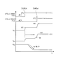
図2は、本発明にかかるインバータ装置におけるゲート駆動回路の実施の形態1の構成を示す回路図である。すなわち、図1に示すゲート駆動回路14a〜14f(代表してゲート駆動回路14と記載)を示す回路図である。図2には、制御回路20、スイッチング素子12、ダイオード13及びゲート駆動回路14が示されている。なお、スイッチング素子12は、図1に示すスイッチング素子12a〜12fのいずれかであり、ダイオード13は、図1に示すダイオード13a〜13fのいずれかである。
FIG. 2 is a circuit diagram showing the configuration of the first embodiment of the gate drive circuit in the inverter device according to the present invention. That is, it is a circuit diagram showing the
制御回路20は、インバータ装置を駆動するためのPWM(Pulse Width Modulation)信号を出力する制御回路であり、例えばマイコンである。また、図2には、直流電源線21、第1のゲート電圧線22及び第2のゲート電圧線23が示されている。
The
直流電源線21は、制御回路20を動作させる直流電源を供給する電源線である。第1のゲート電圧線22は、スイッチング素子12のゲートを駆動するゲート電圧線である。第2のゲート電圧線23は、スイッチング素子12のゲートを駆動するゲート電圧線である。なお、第2のゲート電圧線23の電圧Vcc2は、第1のゲート電圧線22の電圧Vcc1よりも高くする。
The DC
ゲート駆動回路14は、トランジスタ24,25,26,34(Tr1,Tr2,Tr3,Tr4)と、抵抗27,28,29,35,36と、コンデンサ30と、ダイオード33と、を備える。抵抗27の抵抗値R1及び抵抗28の抵抗値R2は、それぞれゲート駆動回路14が動作可能な値に設定されている。トランジスタ34は、nMOSトランジスタである。コンデンサ30は、抵抗28の抵抗値R2とコンデンサ30の容量値C1の積が適切な所定の時定数(主スイッチング素子のターン音時間の1〜10倍)となるように容量値C1を設定する。ゲート抵抗である抵抗29(抵抗値RG)は、スイッチング素子12のゲート端子にノード32により接続されており、抵抗値RGは、抵抗36の抵抗値の2〜10倍とする。なお、ゲート駆動回路14は、スイッチング素子12の1つを駆動する。
The
次に、本実施の形態のインバータ装置の動作について説明する。図1に示すインバータ装置では、制御回路20がオン信号(ハイレベル)を出力すると、トランジスタ24がターンオンし、第1のゲート電圧線22によって、ゲート抵抗29を介してスイッチング素子12のゲート端子を充電する。
Next, the operation of the inverter device of the present embodiment will be described. In the inverter device shown in FIG. 1, when the
ゲート電圧がしきい値電圧以上になるとスイッチング素子12はターンオンするが、このスピードはゲート電圧によって決まる。よって、第1のゲート電圧線22の電圧を制御することによりトランジスタ24がターンオンするスピードを所望のスピードにすることができる。
When the gate voltage becomes equal to or higher than the threshold voltage, the
次に、トランジスタ26がターンオンすると、第2のゲート電圧線23によって、スイッチング素子12のゲート端子が充電される。このとき、R,Cの回路定数は、ミラー効果が終わった後にトランジスタ26がオンするように設定する。そして、上記したように、第2のゲート電圧線23の電圧は第1のゲート電圧線22の電圧よりも高く設定されている(例えば、15V)ため、ターンオンしたスイッチング素子12は、オン直後のわずかな時間には活性化領域で動作するが、すぐに飽和領域に移行するため発生損失を抑えることができる(図3を参照)。図3は、本実施の形態にかかるインバータ装置におけるトランジスタのオンオフ及び電圧の変化を示す第1のタイムチャートである。図3にはトランジスタ24(Tr1)及びトランジスタ26(Tr3)がオンするタイミングと、ノード31(N1)の電圧VN1の変化と、ノード32(N2)の電圧VN2の変化と、トランジスタ12のコレクタ−エミッタ間電圧VCEの変化と、が示されている。なお、図4,5も同様である。
Next, when the
ところで、スイッチング素子12のターンオンのスピードを遅くしたいときには、第1のゲート電圧線22の電圧を低く設定すればよい(例えば、8V)。これにより、スイッチング素子12のゲート端子に充電を開始してからスイッチング素子12のしきい値電圧に達するまでの時間を遅くすることができ、ミラー効果の時間が長くなり、ターンオンのスピードを遅くすることができる(図4を参照)。図4は、本実施の形態にかかるインバータ装置におけるトランジスタのオンオフ及び電圧の変化を示す第2のタイムチャートである。このようにスイッチングのスピード(ターンオンのスピード)を遅くすると、その間にインバータ装置が発生する総スイッチングロスは大きくなるが、インバータ装置が発生する高周波ノイズを小さくすることができる。
By the way, when it is desired to reduce the turn-on speed of the switching
逆に、ターンオンのスピードを速くしたいときには第1のゲート電圧線22の電圧を高く設定すればよい(例えば、12V)。これにより、スイッチング素子12のゲート端子に充電を開始してからスイッチング素子12のしきい値電圧に達するまでの時間を速くすることができ、ミラー効果の時間が短くなり、ターンオンのスピードを速くすることができる(図5を参照)。図5は、本実施の形態にかかるインバータ装置におけるトランジスタのオンオフ及び電圧の変化を示す第3のタイムチャートである。このようにスイッチングのスピード(ターンオンのスピード)を速くすると、その間にインバータ装置が発生する高周波ノイズは大きくなるが、インバータ装置が発生する総スイッチングロスを小さくすることができる。
Conversely, when it is desired to increase the turn-on speed, the voltage of the first
また、スイッチング素子12は、オフ状態からターンオンする短い時間を除けば、第2のゲート電圧線23によって飽和領域でターンオンしており、インバータ動作中に第1のゲート電圧線22の電圧を変化させてもスイッチング時間が変わるだけであり、スイッチング素子12の駆動能力には影響しない。そのため、インバータ動作を停止しなくても第1のゲート電圧線22の電圧を所望の電圧値に変化させることができ、スイッチングスピード(ターンオンのスピード)をインバータ装置の動作中に変化させることができる。
The switching
以上説明したように、第1のゲート電圧線22の電圧を可変として、インバータ装置の動作を停止させることなくスイッチング素子のスイッチングのスピードを変化させることができるため、インバータ装置を備える電気機器を停止させることなく、運転状態に応じて発生ノイズと損失のトレードオフを最適にしつつインバータ駆動を行うことができる。そのため、電気機器の使用の快適性を損なわずに最適なインバータ駆動を行うことができる。
As described above, since the voltage of the first
すなわち、発生ノイズ量が大きいとき(インバータ運転電流(負荷電流)が大きい)ときには、電圧可変の第1のゲート電圧線22の電圧が低くなるように制御してスイッチングのスピードを遅くすると、発生する最大ノイズ量を抑えることができる。そして、インバータ運転電流(負荷電流)が小さいときには、電圧可変の第1のゲート電圧線22の電圧が高くなるように制御してスイッチングのスピードを速くすると、総スイッチングロスを抑えることができる。
In other words, when the amount of generated noise is large (inverter operating current (load current) is large), it is generated when the switching speed is decreased by controlling the voltage of the variable voltage first
本実施の形態によれば、インバータ動作を停止することなく、スイッチングのスピードを変えることができ、負荷電流の大きさに合わせて発生ノイズとスイッチング損失のトレードオフを最適にすることが可能なインバータ装置を得ることができる。 According to the present embodiment, the inverter can change the switching speed without stopping the inverter operation, and can optimize the trade-off between generated noise and switching loss in accordance with the magnitude of the load current. A device can be obtained.
このように、第1のゲート電圧線22の電圧を可変として運転状態に応じて制御することで、例えば、空気調和機のように軽負荷で運転している時間の割合が全体の運転時間に対して大きい電気機器では年間の総消費電力量を抑えることができ、且つ機器に組み込むノイズ対策部品を削減することができるので、製造コストを抑えることができる。
In this way, by controlling the voltage of the first
実施の形態2.
図6は、本発明にかかるインバータ装置の実施の形態2における第1のゲート電圧線22の電圧を生成する回路図の一例を示す図である。
FIG. 6 is a diagram showing an example of a circuit diagram for generating the voltage of the first
第2のゲート電圧線23の電圧Vcc2は第1のゲート電圧線22の電圧Vcc1よりも高く設定されている。コンデンサ40には、第2のゲート電圧線23の電圧Vcc2の電荷が蓄積されている。第2のゲート電圧線23の電圧Vcc2と第1のゲート電圧線22の電圧Vcc1は基準電位GNDが共通であり、降圧コンバータ等の簡易的な回路により第1のゲート電圧線22の電圧Vcc1が生成される。なお、第2のゲート電圧線23の電圧Vcc2は、第1のゲート電圧線22の電圧Vcc1よりも高電圧であればよく、第2のゲート電圧線でなくてもよい。
The voltage V cc2 of the second
図6において、抵抗43,44,45のそれぞれの抵抗値R3,R4,R5は適当な値に設定されている。トランジスタ41,42がオンオフすることにより、第1のゲート電圧線22の電圧Vcc1及び第2のゲート電圧線23の電圧Vcc2が生成される。
In FIG. 6, the resistance values R 3 , R 4 and R 5 of the
本実施の形態のインバータ装置では、制御回路20が、インバータ回路に流れる電流を監視して電流情報を生成し、この電流情報に基づいてトランジスタ41へのパルス信号のデューティ比を変化させることで、第1のゲート電圧線22の電圧を制御することができる。本実施の形態にて説明したように、簡単な構成の回路でスイッチングのスピードを制御することができる。
In the inverter device of the present embodiment, the
実施の形態3.
図7は、本実施の形態にかかる空気調和機の室外ユニットの概略を示す図である。図7には、室外ユニット50、ファン51、圧縮機52及びインバータ装置53が示されている。インバータ装置53は、実施の形態1にて説明したインバータ装置であり、室外ユニット50内の上部に取り付けられており、圧縮機52内のモータ(図1におけるモータ8)を制御することができる。
Embodiment 3 FIG.
FIG. 7 is a diagram showing an outline of the outdoor unit of the air conditioner according to the present embodiment. FIG. 7 shows an
図7に示すように、実施の形態1のインバータ装置は空気調和機に適用することができ、実施の形態1のインバータ装置を適用することで、安価で高性能な空気調和機を得ることができる。 As shown in FIG. 7, the inverter device of Embodiment 1 can be applied to an air conditioner. By applying the inverter device of Embodiment 1, an inexpensive and high-performance air conditioner can be obtained. it can.
本発明に係るインバータ装置は、同じ基準電位の電圧値の違うゲート電圧が2つ設定され、スイッチング素子12のターンオンのときに所望のタイミングで順番にゲートに電圧を印加することで、インバータ動作を停止することなくスイッチング素子12のターンオンのスピードを制御することができる。
In the inverter device according to the present invention, two gate voltages having different voltage values of the same reference potential are set, and when the switching
以上のように、本発明にかかるインバータ装置は、軽負荷で運転している時間の割合が全体の運転時間に対して大きい電気機器に有用であり、特に、空気調和機に適している。 As described above, the inverter device according to the present invention is useful for an electric device in which the ratio of the time of operation with a light load is large relative to the entire operation time, and is particularly suitable for an air conditioner.
1 交流電源、2 リアクトル、3 短絡部、4 整流回路、4a〜4d,13,13a〜13f,17a〜17d,33 ダイオード、5 平滑化部、5a,5b,30,40 コンデンサ、6 インバータ部、7 スイッチ、8 モータ、9 電流検出部、10 電圧検出部、11 制御部、12,12a〜12f スイッチング素子、14,14a〜14f ゲート駆動回路、15,27,28,35,36,43,44,45 抵抗、16 IGBT、20 制御回路、21 直流電源線、22 第1のゲート電圧線、23 第2のゲート電圧線、24,25,26,34,41,42 トランジスタ、29 ゲート抵抗、31,32 ノード、50 室外ユニット、51 ファン、52 圧縮機、53 インバータ装置。 DESCRIPTION OF SYMBOLS 1 AC power supply, 2 Reactor, 3 Short circuit part, 4 Rectifier circuit, 4a-4d, 13, 13a-13f, 17a-17d, 33 Diode, 5 Smoothing part, 5a, 5b, 30, 40 Capacitor, 6 Inverter part, 7 switch, 8 motor, 9 current detection unit, 10 voltage detection unit, 11 control unit, 12, 12a to 12f switching element, 14, 14a to 14f gate drive circuit, 15, 27, 28, 35, 36, 43, 44 , 45 resistance, 16 IGBT, 20 control circuit, 21 DC power supply line, 22 first gate voltage line, 23 second gate voltage line, 24, 25, 26, 34, 41, 42 transistor, 29 gate resistance, 31 , 32 nodes, 50 outdoor units, 51 fans, 52 compressors, 53 inverter devices.
Claims (4)
前記インバータ部の各スイッチング素子のゲート端子にはゲート駆動回路がそれぞれ接続されており、
前記ゲート駆動回路は第1のゲート電圧線と該第1のゲート電圧線より電圧値の高い第2のゲート電圧線を備え、
前記第1のゲート電圧線の電圧値は前記インバータ装置の動作中にも可変であることを特徴とするインバータ装置。 A rectifier circuit that converts an AC power source into a DC power source, a smoothing unit connected to a subsequent stage of the rectifier circuit, a short circuit unit that short-circuits the AC power source via a reactor that improves the power factor of the AC power source, and the smoothing unit An inverter device including an inverter unit that converts direct current from AC into an alternating current and a control unit that controls the inverter unit,
A gate drive circuit is connected to the gate terminal of each switching element of the inverter unit,
The gate driving circuit includes a first gate voltage line and a second gate voltage line having a voltage value higher than that of the first gate voltage line,
The inverter device, wherein the voltage value of the first gate voltage line is variable even during the operation of the inverter device.
前記インバータ装置がモータを回転駆動させることを特徴とする空気調和機。 Comprising the inverter device according to any one of claims 1 to 3,
An air conditioner characterized in that the inverter device rotates a motor.
Priority Applications (4)
| Application Number | Priority Date | Filing Date | Title |
|---|---|---|---|
| JP2014044286A JP2015171226A (en) | 2014-03-06 | 2014-03-06 | inverter device and air conditioner |
| US14/612,521 US9490705B2 (en) | 2014-03-06 | 2015-02-03 | Inverter device and air conditioner |
| EP15155231.2A EP2916458A1 (en) | 2014-03-06 | 2015-02-16 | Inverter device and air conditioner |
| CN201510096329.7A CN104901576B (en) | 2014-03-06 | 2015-03-04 | DC-to-AC converter and air conditioner |
Applications Claiming Priority (1)
| Application Number | Priority Date | Filing Date | Title |
|---|---|---|---|
| JP2014044286A JP2015171226A (en) | 2014-03-06 | 2014-03-06 | inverter device and air conditioner |
Publications (2)
| Publication Number | Publication Date |
|---|---|
| JP2015171226A true JP2015171226A (en) | 2015-09-28 |
| JP2015171226A5 JP2015171226A5 (en) | 2016-08-18 |
Family
ID=52598587
Family Applications (1)
| Application Number | Title | Priority Date | Filing Date |
|---|---|---|---|
| JP2014044286A Pending JP2015171226A (en) | 2014-03-06 | 2014-03-06 | inverter device and air conditioner |
Country Status (4)
| Country | Link |
|---|---|
| US (1) | US9490705B2 (en) |
| EP (1) | EP2916458A1 (en) |
| JP (1) | JP2015171226A (en) |
| CN (1) | CN104901576B (en) |
Cited By (3)
| Publication number | Priority date | Publication date | Assignee | Title |
|---|---|---|---|---|
| WO2023238296A1 (en) * | 2022-06-08 | 2023-12-14 | 三菱電機株式会社 | Electric power conversion device, motor drive device, and refrigeration cycle application apparatus |
| WO2023238293A1 (en) * | 2022-06-08 | 2023-12-14 | 三菱電機株式会社 | Air conditioner |
| WO2023238292A1 (en) * | 2022-06-08 | 2023-12-14 | 三菱電機株式会社 | Power conversion device, motor drive device, and refrigeration cycle applied equipment |
Families Citing this family (7)
| Publication number | Priority date | Publication date | Assignee | Title |
|---|---|---|---|---|
| US9293978B2 (en) * | 2014-01-20 | 2016-03-22 | Cummins Power Generation Ip, Inc. | Split phase power conversion apparatuses, methods and systems |
| KR101905345B1 (en) * | 2014-09-26 | 2018-10-05 | 미쓰비시덴키 가부시키가이샤 | Power conversion device |
| EP3203626B1 (en) * | 2014-09-30 | 2020-11-25 | Mitsubishi Electric Corporation | Power conversion device |
| JP6617571B2 (en) * | 2016-01-14 | 2019-12-11 | 富士電機株式会社 | Semiconductor switching element gate drive circuit |
| JP6831818B2 (en) * | 2018-08-29 | 2021-02-17 | 株式会社Subaru | Power converter |
| CN110690827B (en) * | 2019-09-19 | 2021-02-02 | 江苏邦士医疗科技有限公司 | Isolation type programmable automatic voltage doubling rectifying circuit |
| US10790818B1 (en) * | 2019-09-27 | 2020-09-29 | Infineon Technologies Austria Ag | Slew rate control by adaptation of the gate drive voltage of a power transistor |
Citations (4)
| Publication number | Priority date | Publication date | Assignee | Title |
|---|---|---|---|---|
| JP2002199700A (en) * | 2000-12-25 | 2002-07-12 | Meidensha Corp | Semiconductor power conversion device |
| JP2009071956A (en) * | 2007-09-12 | 2009-04-02 | Mitsubishi Electric Corp | Gate drive circuit |
| JP2011135731A (en) * | 2009-12-25 | 2011-07-07 | Denso Corp | Driver of switching element |
| JP2013118754A (en) * | 2011-12-02 | 2013-06-13 | Mitsubishi Electric Corp | Inverter device and air conditioner equipped with the same |
Family Cites Families (17)
| Publication number | Priority date | Publication date | Assignee | Title |
|---|---|---|---|---|
| JPH10248265A (en) * | 1997-03-06 | 1998-09-14 | I Hitsutsu Kenkyusho:Kk | Power factor improvement circuit |
| JP4432215B2 (en) | 2000-06-05 | 2010-03-17 | 株式会社デンソー | Semiconductor switching element gate drive circuit |
| JP4023336B2 (en) | 2003-02-20 | 2007-12-19 | 株式会社日立製作所 | Method and apparatus for driving semiconductor device |
| WO2004073065A1 (en) | 2003-02-14 | 2004-08-26 | Hitachi, Ltd. | Integrated circuit for driving semiconductor device and power converter |
| JP4323266B2 (en) * | 2003-09-09 | 2009-09-02 | 三菱電機株式会社 | Semiconductor drive circuit |
| JP4823708B2 (en) * | 2006-02-13 | 2011-11-24 | 三菱電機株式会社 | DC power supply |
| JP5186095B2 (en) * | 2006-10-02 | 2013-04-17 | 株式会社日立製作所 | Gate drive circuit |
| JP2007166655A (en) | 2007-02-05 | 2007-06-28 | Hitachi Ltd | Device for driving power semiconductor element |
| JP5298557B2 (en) * | 2008-02-14 | 2013-09-25 | 富士電機株式会社 | Voltage-driven semiconductor device gate drive device |
| JP5065986B2 (en) | 2008-05-12 | 2012-11-07 | 日立オートモティブシステムズ株式会社 | Semiconductor device driving apparatus and driving method thereof |
| WO2010073489A1 (en) * | 2008-12-26 | 2010-07-01 | 株式会社アドバンテスト | Switch device and testing device |
| JP2011120330A (en) * | 2009-12-01 | 2011-06-16 | Mitsubishi Electric Corp | Inverter device and air conditioner with the same |
| CN102439831B (en) * | 2010-07-30 | 2014-04-23 | 丰田自动车株式会社 | Drive device for driving voltage-driven element |
| JP5633442B2 (en) | 2011-03-18 | 2014-12-03 | 三菱電機株式会社 | Inverter control device and refrigeration air conditioner |
| US9231583B2 (en) * | 2011-06-14 | 2016-01-05 | Merus Audio Aps | Power transistor gate driver |
| JP5591213B2 (en) * | 2011-11-25 | 2014-09-17 | 三菱電機株式会社 | Inverter device and air conditioner equipped with the same |
| GB2497970A (en) * | 2011-12-23 | 2013-07-03 | Amantys Ltd | Power semiconductor switching device controller |
-
2014
- 2014-03-06 JP JP2014044286A patent/JP2015171226A/en active Pending
-
2015
- 2015-02-03 US US14/612,521 patent/US9490705B2/en active Active
- 2015-02-16 EP EP15155231.2A patent/EP2916458A1/en not_active Ceased
- 2015-03-04 CN CN201510096329.7A patent/CN104901576B/en active Active
Patent Citations (4)
| Publication number | Priority date | Publication date | Assignee | Title |
|---|---|---|---|---|
| JP2002199700A (en) * | 2000-12-25 | 2002-07-12 | Meidensha Corp | Semiconductor power conversion device |
| JP2009071956A (en) * | 2007-09-12 | 2009-04-02 | Mitsubishi Electric Corp | Gate drive circuit |
| JP2011135731A (en) * | 2009-12-25 | 2011-07-07 | Denso Corp | Driver of switching element |
| JP2013118754A (en) * | 2011-12-02 | 2013-06-13 | Mitsubishi Electric Corp | Inverter device and air conditioner equipped with the same |
Cited By (3)
| Publication number | Priority date | Publication date | Assignee | Title |
|---|---|---|---|---|
| WO2023238296A1 (en) * | 2022-06-08 | 2023-12-14 | 三菱電機株式会社 | Electric power conversion device, motor drive device, and refrigeration cycle application apparatus |
| WO2023238293A1 (en) * | 2022-06-08 | 2023-12-14 | 三菱電機株式会社 | Air conditioner |
| WO2023238292A1 (en) * | 2022-06-08 | 2023-12-14 | 三菱電機株式会社 | Power conversion device, motor drive device, and refrigeration cycle applied equipment |
Also Published As
| Publication number | Publication date |
|---|---|
| CN104901576A (en) | 2015-09-09 |
| CN104901576B (en) | 2017-06-23 |
| US9490705B2 (en) | 2016-11-08 |
| US20150256083A1 (en) | 2015-09-10 |
| EP2916458A1 (en) | 2015-09-09 |
Similar Documents
| Publication | Publication Date | Title |
|---|---|---|
| JP2015171226A (en) | inverter device and air conditioner | |
| US9806594B2 (en) | Drive device for power converter and driving method of power converter | |
| JP5928946B2 (en) | Rectification circuit and motor drive device using the same | |
| JP2015171226A5 (en) | ||
| US20160079904A1 (en) | Drive unit employing gallium nitride switches | |
| JP5471384B2 (en) | Inverter device for motor drive | |
| JP5032184B2 (en) | Motor control circuit | |
| JP6384316B2 (en) | Power converter and control method of power converter | |
| KR101911262B1 (en) | Power transforming apparatus having noise reduction function and air conditioner including the same | |
| JP4300209B2 (en) | Inverter device | |
| KR102174638B1 (en) | Power transforming apparatus having noise reduction function, compressor including the same and the method for the same | |
| WO2020066028A1 (en) | Motor drive device and air conditioner | |
| US6548983B2 (en) | PWM-pulse control system | |
| JP5353468B2 (en) | Power converter | |
| KR102007852B1 (en) | Power transforming apparatus and air conditioner including the same | |
| KR102069068B1 (en) | Power transforming apparatus, Method for controlling the same and Air conditioner including the power transforming apparatus | |
| JP5101001B2 (en) | Inverter device | |
| KR101946369B1 (en) | Power transforming apparatus and air conditioner including the same | |
| JP2016046935A (en) | Semiconductor device, and converter using the same, inverter, air conditioner, solar power controller and automobile | |
| KR102036113B1 (en) | Power transforming apparatus and air conditioner including the same | |
| JP2013135516A (en) | Electric power conversion system and air conditioner | |
| KR20190021672A (en) | Power transforming apparatus and air conditioner including the same | |
| KR20190019331A (en) | Power transforming apparatus, air conditioner including the same and method for controlling the same | |
| KR102160049B1 (en) | Power transforming apparatus and air conditioner including the same | |
| JP2007236090A (en) | Method and apparatus for controlling brushless motor |
Legal Events
| Date | Code | Title | Description |
|---|---|---|---|
| A521 | Request for written amendment filed |
Free format text: JAPANESE INTERMEDIATE CODE: A523 Effective date: 20160630 |
|
| A621 | Written request for application examination |
Free format text: JAPANESE INTERMEDIATE CODE: A621 Effective date: 20160630 |
|
| A977 | Report on retrieval |
Free format text: JAPANESE INTERMEDIATE CODE: A971007 Effective date: 20170412 |
|
| A131 | Notification of reasons for refusal |
Free format text: JAPANESE INTERMEDIATE CODE: A131 Effective date: 20170418 |
|
| A521 | Request for written amendment filed |
Free format text: JAPANESE INTERMEDIATE CODE: A523 Effective date: 20170523 |
|
| A02 | Decision of refusal |
Free format text: JAPANESE INTERMEDIATE CODE: A02 Effective date: 20170718 |