JP2013197108A - Laser processing method for wafer - Google Patents
Laser processing method for wafer Download PDFInfo
- Publication number
- JP2013197108A JP2013197108A JP2012059121A JP2012059121A JP2013197108A JP 2013197108 A JP2013197108 A JP 2013197108A JP 2012059121 A JP2012059121 A JP 2012059121A JP 2012059121 A JP2012059121 A JP 2012059121A JP 2013197108 A JP2013197108 A JP 2013197108A
- Authority
- JP
- Japan
- Prior art keywords
- laser beam
- wafer
- energy
- teg
- division line
- Prior art date
- Legal status (The legal status is an assumption and is not a legal conclusion. Google has not performed a legal analysis and makes no representation as to the accuracy of the status listed.)
- Pending
Links
- 238000003672 processing method Methods 0.000 title claims abstract description 19
- 230000002265 prevention Effects 0.000 claims abstract description 30
- 238000009826 distribution Methods 0.000 claims abstract description 21
- 230000001678 irradiating effect Effects 0.000 claims abstract description 8
- 238000000034 method Methods 0.000 claims description 3
- 239000012212 insulator Substances 0.000 abstract description 2
- 235000012431 wafers Nutrition 0.000 description 44
- 239000004065 semiconductor Substances 0.000 description 29
- 238000005520 cutting process Methods 0.000 description 20
- 230000010287 polarization Effects 0.000 description 19
- 230000003287 optical effect Effects 0.000 description 14
- 229910004298 SiO 2 Inorganic materials 0.000 description 5
- 230000015572 biosynthetic process Effects 0.000 description 5
- 229910052751 metal Inorganic materials 0.000 description 5
- 239000002184 metal Substances 0.000 description 5
- VYPSYNLAJGMNEJ-UHFFFAOYSA-N Silicium dioxide Chemical compound O=[Si]=O VYPSYNLAJGMNEJ-UHFFFAOYSA-N 0.000 description 4
- XUIMIQQOPSSXEZ-UHFFFAOYSA-N Silicon Chemical compound [Si] XUIMIQQOPSSXEZ-UHFFFAOYSA-N 0.000 description 4
- 238000003384 imaging method Methods 0.000 description 4
- 239000011229 interlayer Substances 0.000 description 4
- -1 polytetrafluoroethylene Polymers 0.000 description 4
- 229910052710 silicon Inorganic materials 0.000 description 4
- 239000010703 silicon Substances 0.000 description 4
- 238000001514 detection method Methods 0.000 description 3
- 238000010586 diagram Methods 0.000 description 3
- 239000010410 layer Substances 0.000 description 3
- 238000003754 machining Methods 0.000 description 3
- 230000001105 regulatory effect Effects 0.000 description 3
- RYGMFSIKBFXOCR-UHFFFAOYSA-N Copper Chemical compound [Cu] RYGMFSIKBFXOCR-UHFFFAOYSA-N 0.000 description 2
- 239000004642 Polyimide Substances 0.000 description 2
- 229910009372 YVO4 Inorganic materials 0.000 description 2
- 229910052782 aluminium Inorganic materials 0.000 description 2
- XAGFODPZIPBFFR-UHFFFAOYSA-N aluminium Chemical compound [Al] XAGFODPZIPBFFR-UHFFFAOYSA-N 0.000 description 2
- 229910052802 copper Inorganic materials 0.000 description 2
- 239000010949 copper Substances 0.000 description 2
- 239000013078 crystal Substances 0.000 description 2
- 230000000694 effects Effects 0.000 description 2
- 230000006870 function Effects 0.000 description 2
- 238000003331 infrared imaging Methods 0.000 description 2
- 125000002496 methyl group Chemical group [H]C([H])([H])* 0.000 description 2
- 229920000052 poly(p-xylylene) Polymers 0.000 description 2
- 229920001721 polyimide Polymers 0.000 description 2
- 229920006254 polymer film Polymers 0.000 description 2
- 229920001296 polysiloxane Polymers 0.000 description 2
- 229920001343 polytetrafluoroethylene Polymers 0.000 description 2
- 239000004810 polytetrafluoroethylene Substances 0.000 description 2
- 239000000377 silicon dioxide Substances 0.000 description 2
- 239000000758 substrate Substances 0.000 description 2
- JBRZTFJDHDCESZ-UHFFFAOYSA-N AsGa Chemical compound [As]#[Ga] JBRZTFJDHDCESZ-UHFFFAOYSA-N 0.000 description 1
- 229910001218 Gallium arsenide Inorganic materials 0.000 description 1
- 239000002390 adhesive tape Substances 0.000 description 1
- 229910003460 diamond Inorganic materials 0.000 description 1
- 239000010432 diamond Substances 0.000 description 1
- 229910010272 inorganic material Inorganic materials 0.000 description 1
- 239000011147 inorganic material Substances 0.000 description 1
- 238000004519 manufacturing process Methods 0.000 description 1
- 239000000463 material Substances 0.000 description 1
- 239000010445 mica Substances 0.000 description 1
- 229910052618 mica group Inorganic materials 0.000 description 1
- 230000003071 parasitic effect Effects 0.000 description 1
- 238000000059 patterning Methods 0.000 description 1
- 230000002093 peripheral effect Effects 0.000 description 1
- 239000011347 resin Substances 0.000 description 1
- 229920005989 resin Polymers 0.000 description 1
- 238000000926 separation method Methods 0.000 description 1
Images


Abstract
Description
本発明は、層間絶縁膜として低誘電率絶縁膜(Low−k膜)を使用したウエーハのレーザー加工方法に関する。 The present invention relates to a wafer laser processing method using a low dielectric constant insulating film (Low-k film) as an interlayer insulating film.
半導体デバイス製造プロセスにおいては、略円板形状であるシリコンウエーハ、ガリウム砒素ウエーハ等の半導体ウエーハの表面に格子状に形成されたストリートと呼ばれる分割予定ラインによって複数の領域が区画され、区画された各領域にIC、LSI等のデバイスを形成する。 In the semiconductor device manufacturing process, a plurality of regions are defined by dividing lines called streets formed in a lattice shape on the surface of a semiconductor wafer such as a silicon wafer or a gallium arsenide wafer having a substantially disk shape. A device such as an IC or LSI is formed in the region.
このような半導体ウエーハは研削装置によって裏面が研削されて所定の厚みに加工された後、切削装置又はレーザー加工装置によって個々のデバイスに分割され、分割されたデバイスは携帯電話、パソコン等の各種電気機器に広く利用されている。 After such a semiconductor wafer is ground to a predetermined thickness by a grinding device and then processed into a predetermined thickness, the semiconductor wafer is divided into individual devices by a cutting device or a laser processing device. Widely used in equipment.
切削装置としては一般にダイシング装置と呼ばれる切削装置が用いられており、この切削装置ではダイアモンドやCBN等の超砥粒をメタルやレジンで固めて厚さ20〜30μmの切刃を有する切削ブレードが約30000rpm等の高速で回転しつつ半導体ウエーハへ切り込むことで切削が遂行される。 As a cutting device, a cutting device generally called a dicing device is used. In this cutting device, a cutting blade having a cutting blade with a thickness of 20 to 30 μm is obtained by solidifying superabrasive grains such as diamond and CBN with metal or resin. Cutting is performed by cutting into a semiconductor wafer while rotating at a high speed such as 30000 rpm.
半導体ウエーハの表面に形成された半導体デバイスは、金属配線が何層にも積層されて信号を伝達しており、各金属配線間は主にSiO2から形成された層間絶縁膜により絶縁されている。 A semiconductor device formed on the surface of a semiconductor wafer has a plurality of layers of metal wirings that transmit signals, and each metal wiring is insulated by an interlayer insulating film formed mainly of SiO 2 . .
近年、構造の微細化に伴い、配線間距離が近くなり、近接する配線間の電気容量は大きくなってきている。これに起因して信号の遅延が発生し、消費電力が増加するという問題が顕著になってきている。 In recent years, with the miniaturization of the structure, the distance between wirings has become shorter, and the electric capacity between adjacent wirings has increased. Due to this, a problem that signal delay occurs and power consumption increases has become prominent.
各層間の寄生容量を軽減すべく、デバイス(回路)形成時に各層間を絶縁する層間絶縁膜として従来は主にSiO2絶縁膜を採用していたが、最近になりSiO2絶縁膜よりも誘電率の低い低誘電率絶縁膜(Low−k膜)が採用されるようになってきている。 In order to reduce the parasitic capacitance between the layers, the device (circuit) prior to each layer when forming an interlayer insulating film for insulating primarily had adopted the SiO 2 insulating film, than recently become SiO 2 insulating film dielectric A low dielectric constant insulating film (Low-k film) having a low rate has been adopted.
低誘電率絶縁膜としては、SiO2膜(誘電率k=4.1)よりも誘電率が低い(例えばk=2.5乃至3.6程度)材料、例えばSiOC,SiLK等の無機物系の膜、ポリイミド系、パリレン系、ポリテトラフルオロエチレン系等のポリマー膜である有機物系の膜、及びメチル含有ポリシロキサン等のポーラスシリカ膜を挙げることができる。 As the low dielectric constant insulating film, a material having a dielectric constant lower than that of the SiO 2 film (dielectric constant k = 4.1) (for example, about k = 2.5 to 3.6), for example, an inorganic material such as SiOC, SiLK, etc. Examples thereof include organic films such as films, polyimide-based, parylene-based, and polytetrafluoroethylene-based polymer films, and porous silica films such as methyl-containing polysiloxane.
このような低誘電率絶縁膜を含む積層体を切削ブレードにより分割予定ラインに沿って切削すると、低誘電率絶縁膜は雲母のように非常に脆いことから積層体が剥離するという問題が生じる。 When a laminated body including such a low dielectric constant insulating film is cut along a line to be divided by a cutting blade, the low dielectric constant insulating film is very brittle like mica, which causes a problem that the laminated body is peeled off.
この問題を解決するために、例えば特開2005−064230号公報又は特開2005−209719号公報では、切削ブレードでの切削に先立って、予め分割予定ライン上の積層体をレーザービームの照射により除去し、その後切削ブレードでチップへと分割する半導体ウエーハの加工方法が提案されている。 In order to solve this problem, for example, in Japanese Patent Application Laid-Open No. 2005-064230 or Japanese Patent Application Laid-Open No. 2005-209719, prior to cutting with a cutting blade, the laminated body on the planned division line is removed in advance by laser beam irradiation. Then, a semiconductor wafer processing method in which the wafer is divided into chips with a cutting blade has been proposed.
しかし、低誘電率絶縁膜(Low−k膜)の分断にはある程度のエネルギー密度が必要であるため、通常レーザービームを円形スポットに集光し、ある程度のエネルギー密度のあるレーザービームを分割予定ラインの両端付近に照射して加工する必要があるため、少なくとも一本の分割予定ラインを2回走査させる必要がある。 However, since a certain amount of energy density is required to divide the low dielectric constant insulating film (Low-k film), the laser beam is usually focused on a circular spot, and the laser beam with a certain energy density is scheduled to be split. Therefore, it is necessary to scan at least one division planned line twice.
また、分割予定ライン上には通常TEG(Test Element Group)と呼ばれる試験用の回路が形成されており、TEGは例えばアルミニウムや銅等の金属から形成されているため、Low−k膜やシリコンと比較すると加工が難しい。 In addition, a test circuit called a test element group (TEG) is usually formed on the planned division line. Since the TEG is made of a metal such as aluminum or copper, a low-k film or silicon is used. Processing is difficult when compared.
よって、レーザービームの照射によりTEGを除去するには非常に高いエネルギーが必要であり、切削ブレードでTEGを切削するとブレードの目詰まりの原因となり、突発的な欠け(チッピング)を発生させる要因となる。 Therefore, very high energy is required to remove TEG by laser beam irradiation, and cutting the TEG with a cutting blade causes clogging of the blade and causes sudden chipping (chipping). .
そのため、切削ブレードによるTEGの切削の前に、事前にレーザービームを照射してTEGを除去することが望ましい。よって、一本の分割予定ラインに対して合計3回のレーザービームの走査が必要である。 Therefore, it is desirable to remove the TEG by irradiating a laser beam in advance before cutting the TEG with the cutting blade. Therefore, it is necessary to scan the laser beam three times in total with respect to one division planned line.
本発明はこのような点に鑑みてなされたものであり、その目的とするところは、一本の分割予定ラインに対して2回のレーザービームの走査により、Low−k膜及びTEGの除去が可能なウエーハのレーザー加工方法を提供することである。 The present invention has been made in view of the above points, and the object of the present invention is to remove the Low-k film and the TEG by scanning the laser beam twice with respect to one division planned line. It is to provide a possible wafer laser processing method.
本発明によると、表面に低誘電率絶縁膜を含む積層体が積層され、該積層体によって格子状に交差する一部にTEGが形成された複数の分割予定ラインと該分割予定ラインで区画された各領域にデバイスが形成されたウエーハに、ガウシアン分布のエネルギー強度分布を有するレーザービームを該分割予定ラインに沿って照射して、レーザー加工溝を形成するウエーハのレーザー加工方法であって、該分割予定ラインの幅方向に対して所定の幅で溝が形成されるように、第1のビーム径を有する第1レーザービームを通過範囲を規制するマスクを介して、該分割予定ラインに沿って照射して、該分割予定ラインに1条の膜剥がれ防止溝を形成する膜剥がれ防止溝形成ステップと、該第1のビーム径より小さい第2のビーム径を有し該第1レーザービームのエネルギー量と同等のエネルギー量を有する第2レーザービームを、該マスクを介して該分割予定ラインに沿って照射して、該分割予定ラインに1条のTEG除去用溝を形成するTEG除去用溝形成ステップと、を備え、該第1レーザービームはなだらかなガウシアン分布を有しており、該マスクを通過した該第1レーザービームの該分割予定ラインの幅方向両端部のエネルギー量は該膜剥がれ防止溝を形成するのに十分な第1のエネルギー量であり、該第2レーザービームは該第1レーザービームに比較して急峻なガウシアン分布を有しており、該マスクを通過した該第2レーザービームの該分割予定ラインの幅方向両端部のエネルギー量は該第1のエネルギー量より低く、中央部分のエネルギー量は該第1のエネルギー量より高く該TEG除去用溝を形成するのに十分な第2のエネルギー量であることを特徴とするウエーハのレーザー加工方法が提供される。 According to the present invention, a laminate including a low dielectric constant insulating film is laminated on the surface, and the laminate is partitioned by a plurality of scheduled division lines in which TEGs are formed in a part intersecting in a lattice shape and the scheduled division lines. A wafer laser processing method for forming a laser processing groove by irradiating a wafer having a device formed in each region with a laser beam having an energy intensity distribution of Gaussian distribution along the planned division line, The first laser beam having the first beam diameter is passed along the planned division line through a mask that restricts the passage range of the first laser beam so that a groove is formed with a predetermined width in the width direction of the planned division line. A film peeling prevention groove forming step of irradiating to form one film peeling prevention groove on the line to be divided; and a second beam diameter smaller than the first beam diameter, -TEG removal for irradiating a second laser beam having an energy amount equivalent to the energy amount of the beam along the planned division line through the mask to form one TEG removal groove on the planned division line The first laser beam has a gentle Gaussian distribution, and the amount of energy at both ends in the width direction of the division line of the first laser beam that has passed through the mask is The first energy amount is sufficient to form a film peeling prevention groove, and the second laser beam has a steep Gaussian distribution compared to the first laser beam, and passes through the mask. The amount of energy at both ends in the width direction of the line to be split of the second laser beam is lower than the first amount of energy, and the amount of energy at the center is equal to the first amount of energy. Laser processing method of the wafer, wherein the higher is the second energy amount sufficient to form the TEG removing grooves are provided.
本発明のレーザー加工方法によると、レーザービームのビーム径を太いビーム径と細いビーム径に選択的に変更してから、両方のレーザービームをマスクのスリットを通過させるため、スリット通過後のレーザービームのエネルギー分布を分割予定ラインの幅方向で調整することができ、一本の膜剥がれ防止溝の形成と一本のTEG除去用溝の形成によって従来の3回のレーザービームの走査と同等の効果を得ることができる。 According to the laser processing method of the present invention, after selectively changing the beam diameter of the laser beam to a thick beam diameter and a thin beam diameter, both laser beams pass through the slit of the mask. Energy distribution can be adjusted in the width direction of the line to be divided, and by forming one film peeling prevention groove and one TEG removal groove, the same effect as the conventional three times of laser beam scanning Can be obtained.
大きなビーム径のレーザービームは、マスクのスリットを通過した後分割予定ラインの幅方向両端部のエネルギー量が比較的高い状態でウエーハに照射することができるため、十分にLow−k膜の分断が可能であり、小さなビーム径のレーザービームは、マスクのスリットを通過後中央に高いエネルギー量を有する状態でウエーハに照射されるため、比較的高いエネルギー量を要するTEGの除去を十分に行うことができ、且つレーザー加工溝の縁はエネルギー密度が小さいため、不要に加工溝の岸を加工しないという効果も奏する。 Since the laser beam with a large beam diameter can be irradiated to the wafer with a relatively high energy amount at both ends in the width direction of the line to be divided after passing through the slit of the mask, the low-k film is sufficiently divided. A laser beam having a small beam diameter can be irradiated to the wafer in a state having a high energy amount in the center after passing through the slit of the mask. Therefore, it is possible to sufficiently remove the TEG that requires a relatively high energy amount. In addition, since the energy density of the edge of the laser processing groove is small, there is an effect that the processing groove is not processed unnecessarily.
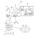
以下、本発明の実施形態を図面を参照して詳細に説明する。図1を参照すると、本発明のウエーハのレーザー加工方法を実施するのに適したレーザー加工装置2の斜視図が示されている。レーザー加工装置2は、静止基台4上にX軸方向に移動可能に搭載された第1スライドブロック6を含んでいる。
Hereinafter, embodiments of the present invention will be described in detail with reference to the drawings. Referring to FIG. 1, there is shown a perspective view of a
第1スライドブロック6は、ボールねじ8及びパルスモータ10から構成される加工送り手段12により一対のガイドレール14に沿って加工送り方向、即ちX軸方向に移動される。
The first slide block 6 is moved in the machining feed direction, that is, the X-axis direction along the pair of
第1スライドブロック6上には第2スライドブロック16がY軸方向に移動可能に搭載されている。すなわち、第2スライドブロック16はボールねじ18及びパルスモータ20から構成される割り出し送り手段22により一対のガイドレール24に沿って割り出し方向、すなわちY軸方向に移動される。
A
第2スライドブロック16上には円筒支持部材26を介してチャックテーブル28が搭載されており、チャックテーブル28は加工送り手段12及び割り出し送り手段22によりX軸方向及びY軸方向に移動可能である。チャックテーブル28には、チャックテーブル28に吸引保持された半導体ウエーハをクランプするクランプ30が設けられている。
A chuck table 28 is mounted on the
静止基台4にはコラム32が立設されており、このコラム32にレーザービーム照射ユニット34が取り付けられている。レーザービーム照射ユニット34は、ケーシング33中に収容された図2に示すレーザービーム発生ユニット35と、ケーシング33の先端に取り付けられた集光器37とを含んでいる。
A
レーザービーム発生ユニット35は、図2に示すように、YAGレーザー又はYVO4レーザーを発振するレーザー発振器62と、繰り返し周波数設定手段64と、パルス幅調整手段66と、パワー調整手段68とを含んでいる。特に図示しないが、レーザー発振器62はブリュースター窓を有しており、レーザー発振器62から出射するレーザービームは直線偏光のレーザービームである。
As shown in FIG. 2, the laser
ケーシング33の先端部には、集光器37とX軸方向に整列してレーザー加工すべき加工領域を検出する撮像手段39が配設されている。撮像手段39は、可視光によって半導体ウエーハの加工領域を撮像する通常のCCD等の撮像素子を含んでいる。
An image pickup means 39 for detecting a processing region to be laser processed in alignment with the
撮像手段39は更に、半導体ウエーハに赤外線を照射する赤外線照射手段と、赤外線照射手段によって照射された赤外線を捕らえる光学系と、この光学系によって捕らえられた赤外線に対応した電気信号を出力する赤外線CCD等の赤外線撮像素子から構成される赤外線撮像手段を含んでおり、撮像した画像信号はコントローラ(制御手段)40に送信される。 The imaging means 39 further includes an infrared irradiation means for irradiating the semiconductor wafer with infrared rays, an optical system for capturing the infrared rays irradiated by the infrared irradiation means, and an infrared CCD for outputting an electrical signal corresponding to the infrared rays captured by the optical system. Infrared imaging means composed of an infrared imaging element such as the above is included, and the captured image signal is transmitted to a controller (control means) 40.
コントローラ40はコンピュータによって構成されており、制御プログラムに従って演算処理する中央処理装置(CPU)42と、制御プログラム等を格納するリードオンリーメモリ(ROM)44と、演算結果等を格納する読み書き可能なランダムアクセスメモリ(RAM)46と、カウンタ48と、入力インターフェイス50と、出力インターフェイス52とを備えている。
The
56は案内レール14に沿って配設されたリニアスケール54と、第1スライドブロック6に配設された図示しない読み取りヘッドとから構成される加工送り量検出手段であり、加工送り量検出手段56の検出信号はコントローラ40の入力エンターフェイス50に入力される。
60はガイドレール24に沿って配設されたリニアスケール58と第2スライドブロック16に配設された図示しない読み取りヘッドとから構成される割り出し送り量検出手段であり、割り出し送り量検出手段60の検出信号はコントローラ40の入力インターフェイス50に入力される。
撮像手段39で撮像した画像信号もコントローラ40の入力インターフェイス50に入力される。一方、コントローラ40の出力インターフェイス52からはパルスモータ10、パルスモータ20、レーザービーム照射ユニット34等に制御信号が出力される。
An image signal picked up by the image pickup means 39 is also input to the
図2を参照すると、レーザービーム照射ユニット34の構成ブロック図が示されている。レーザービーム発生ユニット35のパワー調整手段68で所定パワーに調整された直線偏光のレーザービームLBは1/2波長板70に入射される。
Referring to FIG. 2, a configuration block diagram of the laser
1/2波長板70は図示しない回転機構により回転可能に配設されており、波長板の結晶の光学軸に対して角度θで入射された直線偏光の偏光面を−θ回転して出射する。即ち、1/2波長板70をθ回転すると、入射された直線偏光の偏光面が2θ回転されて1/2波長板70から出射される。
The half-
1/2波長板70から出射されたパルスレーザービームLBは偏光ビームスプリッター72に入射され、P偏光(P波)は偏光ビームスプリッター72を透過し、S偏光(S波)は偏光ビームスプリッター72で反射される。
The pulsed laser beam LB emitted from the half-
よって、1/2波長板70を適当に回転することにより、パルスレーザービームLBの偏光面を任意に回転することができ、偏光ビームスプリッター72によって第1の光路74aを通るP偏光からなる第1のパルスレーザービームLB1と第2の光路74bを通るS偏光からなる第2のパルスレーザービームLB2の比率を変更することができる。
Therefore, by appropriately rotating the half-
1/2波長板70はその結晶の光学軸がレーザービーム発生ユニット35から出射されるパルスレーザービームLBの偏光面と平行な状態を回転角0度として配設される。例えば、レーザービーム発生ユニット35から出射されるパルスレーザービームLBがP偏光の場合には、回転角0度の1/2波長板70をP偏光のまま透過し、更に偏光ビームスプリッター72を透過して第1のパルスレーザービームLB1として第1の光路74aに導かれる。
The half-
一方、1/2波長板70を45度回転すると、1/2波長板70からは偏光面が90度回転されたS偏光が出射される。このS偏光のパルスレーザービームLBは偏光ビームスプリッター72でほぼ完全に反射されて、第2のパルスレーザービームLB2として第2の光路74bに導かれる。
On the other hand, when the half-
よって、1/2波長板70の回転角が0度の場合には、レーザービーム発生ユニット35から出射されたP偏光のパルスレーザービームLBはほぼ全てが第1のパルスレーザービームLB1として第1の光路74aに導かれ、1/2波長板70を45度回転すると、レーザービーム発生ユニット35から出射されたパルスレーザービームLBはそのほぼ全てがS偏光の第2のパルスレーザービームLB2として第2の光路74bに導かれる。
Therefore, when the rotation angle of the half-
第1のパルスレーザービームLB1はミラー76で反射され第1ビーム径調整手段78に入射される。第1ビーム径調整手段78は、図4(A)に示すように、凹レンズ94と凸レンズ96をこの順で組み合わせて構成されており、間隔調整手段98で凹レンズ94及び凸レンズ96を矢印Z1方向に移動することにより、入射された第1のパルスレーザービームLB1のビーム径を所望のビーム径に拡大して出射することができる。よって、第1ビーム径調整手段78はビーム径拡大手段として作用する。
The first pulse laser beam LB 1 is reflected by the
一方、偏光ビームスプリッター72で反射された第2のパルスレーザービームLB2は、第2の光路74bに配設された第2ビーム径調整手段82に入射される。第2ビーム径調整手段82は、図4(B)に示すように、凸レンズ100と凹レンズ102をこの順で組み合わせて構成されており、間隔調整手段104で凸レンズ100及び凹レンズ102を矢印Z2方向に移動することにより、入射された第2のパルスレーザービームLB2のビーム径を所望のビーム径に縮小して出射することができる。よって、第2ビーム径調整手段82はビーム径縮小手段として作用する。
On the other hand, the second pulse laser beam LB2 reflected by the
第1ビーム径調整手段78から出射されたビーム径の拡大された第1のパルスレーザービームLB1はP偏光であるので、偏光ビームスプリッター80を透過して集光器37に入射される。
Since the first pulse laser beam LB1 with the expanded beam diameter emitted from the first beam diameter adjusting means 78 is P-polarized light, it passes through the
一方、第2ビーム径調整手段82から出射された第2のパルスレーザービームLB2はミラー84で偏光ビームスプリッター80方向に反射され、第2のパルスレーザービームLB2はS偏光であるから偏光ビームスプリッター80で反射されて集光器37に入射される。
On the other hand, the second pulse laser beam LB2 emitted from the second beam diameter adjusting means 82 is reflected by the
集光器37は、スリット87を有するマスク86と、結像用補助レンズ88と、集光レンズ90とを含んでいる。スリット87は例えば長方形状をしており、その長手方向がレーザービームの走査方向と平行となる様に集光器37に取り付けられている。
The
図3を参照すると、マスク86からウエーハ11上の加工点までのパルスレーザービームの状態を模式的に示す説明図が示されている。マスク86のスリット87を通過したパルスレーザービームLBは結像用補助レンズ88でコリメートビームに変換されてから集光レンズ90に入射し、集光レンズ90でウエーハ11上に集光される。
Referring to FIG. 3, there is shown an explanatory diagram schematically showing the state of the pulse laser beam from the
ウエーハ11上での結像状態の悪化を防止するために、結像用補助レンズ88がマスク86と集光レンズ90との間に挿入されている。92a,92bはパルスレーザービームLBのエネルギー分布を示している。
In order to prevent the image forming state on the
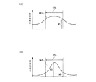
次に、図5を参照して、第1ビーム径調整手段78及び第2ビーム径調整手段82通過後の、第1のパルスレーザービームLB1及び第2のパルスレーザービームLB2のエネルギー分布について説明する。 Next, the energy distribution of the first pulse laser beam LB1 and the second pulse laser beam LB2 after passing through the first beam diameter adjusting means 78 and the second beam diameter adjusting means 82 will be described with reference to FIG. .
図5(A)は、第1ビーム径調整手段78でビーム径が拡大された第1のパルスレーザービームLB1のエネルギー分布であり、図5(B)は、第2ビーム径調整手段82を通過してビーム径が縮小された第2のパルスレーザービームLB2のビーム径をそれぞれ示している。87Aはマスク86のスリット87を通過したスリット領域を示している。
5A shows the energy distribution of the first pulse laser beam LB1 whose beam diameter has been expanded by the first beam diameter adjusting means 78, and FIG. 5B passes through the second beam diameter adjusting means 82. FIG. The beam diameters of the second pulse laser beam LB2 whose beam diameter is reduced are shown.
図5(A)に示すビーム径が拡大された大径の第1のパルスレーザービームLB1はエネルギーのガウシアン分布がなだらかであり、スリット領域87Aで規制される加工に用いるレーザービームの範囲の両端側で比較的高いエネルギーP1となっている。
The large-diameter first pulsed laser beam LB1 with an enlarged beam diameter shown in FIG. 5A has a gentle Gaussian distribution of energy, and both ends of the range of the laser beam used for processing regulated by the
一方、図5(B)に示すビーム径が縮小された小径の第2のパルスレーザービームLB2はエネルギーのガウシアン分布が急峻であり、その中央部分で非常に高いエネルギーP2を維持しているが、マスク領域87Aで規制される加工に用いるレーザービームの範囲の両端側で低いエネルギーP3となっている。
On the other hand, the small-diameter second pulse laser beam LB2 with a reduced beam diameter shown in FIG. 5B has a steep Gaussian distribution of energy and maintains a very high energy P2 in the central portion thereof. The energy P3 is low at both ends of the range of the laser beam used for processing regulated by the
スリット領域87Aで規制される加工に用いるレーザービームの範囲内では、第1のパルスレーザービームLB1と第2のパルスレーザービームLB2のエネルギー量は概略同等である。
Within the range of the laser beam used for processing regulated by the
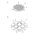
次に、図6及び図10(A)を参照して、本発明のレーザー加工方法の加工対象となる半導体ウエーハ11について説明する。半導体ウエーハ11は、図10(A)に示すように、ウエーハ形状のシリコン基板19上に低誘電率絶縁膜(Low−k膜)を含む積層体21が積層され、積層体21に複数の分割予定ライン13が格子状に形成されているとともに、分割予定ライン13によって区画された各領域に半導体デバイス15がパターニングによって形成されている。
Next, with reference to FIGS. 6 and 10A, a
ここで、低誘電率絶縁膜(Low−k膜)は、誘電率k=約4.1のSiO2膜よりも誘電率が低い絶縁体を指し、例えばSiOC、SiLK、BSG(SiOB)等の無機物系の膜、ポリイミド系、パリレン系、ポリテトラフルオロエチレン系等のポリマー膜である有機物系の膜、及びメチル含有ポリシロキサン等のポーラスシリカ膜を挙げることができる。 Here, the low dielectric constant insulating film (Low-k film) refers to an insulator having a dielectric constant lower than that of the SiO 2 film having a dielectric constant k = about 4.1, such as SiOC, SiLK, BSG (SiOB), etc. An inorganic film, an organic film that is a polymer film such as polyimide, parylene, or polytetrafluoroethylene, and a porous silica film such as methyl-containing polysiloxane can be given.
図6(A)のA部分の拡大図である図6(B)に示すように、分割予定ライン13上には通常TEG(Test Element Group)17と呼ばれる試験用の回路が形成されている。TEG17は例えばアルミニウムや銅等の金属から形成されている。
As shown in FIG. 6B, which is an enlarged view of the portion A in FIG. 6A, a test circuit called a test element group (TEG) 17 is usually formed on the planned
レーザー加工を実施するにあたり、半導体ウエーハ11は、図7に示すように、粘着テープであるダイシングテープTに貼着され、ダイシングテープTの外周部は環状フレームFに貼着される。
In carrying out laser processing, the
これにより、半導体ウエーハ11はダイシングテープTを介して環状フレームFに支持された状態となり、図1に示すチャックテーブル28上に半導体ウエーハ11をダイシングテープTを介して吸引保持し、環状フレームFをクランプ30によりクランプすることにより、チャックテーブル28上に支持固定される。
As a result, the
本実施形態のウエーハのレーザー加工方法では、レーザービーム発生ユニット35により積層体21に対して吸収性を有する波長のパルスレーザービームLBを発生し、膜剥がれ防止溝形成ステップでは、1/2波長板70を回転させずにP偏光のパルスレーザービームLBをそのまま1/2波長板70を透過させ、更に偏光ビームスプリッター72を透過させて第1の光路74aに第1のパルスレーザービームLB1を導く。
In the wafer laser processing method of the present embodiment, the laser
そして、第1ビーム径調整手段78でビーム径を拡大し、更に集光器37のスリット87を透過したパルスレーザービームを集光レンズ92によりウエーハ11の分割予定ライン13に対応する積層体21に集光して、積層体21を分断する1条の膜剥がれ防止溝を形成する膜剥がれ防止溝形成ステップを実施する。
The beam diameter is enlarged by the first beam diameter adjusting means 78, and the pulse laser beam transmitted through the
この膜剥がれ防止溝形成ステップを実施する前に、撮像手段39で半導体ウエーハ11を撮像して、パターンマッチング等の画像処理を実施することによりレーザー加工すべき第1の方向に伸長する分割予定ライン13を検出するアライメントを実施する。
Before carrying out this film peeling prevention groove forming step, the image of the
第1の方向に伸長する分割予定ライン13のアライメントに続いて、チャックテーブル28を90度回転してから、第1の方向と直交する方向に伸長する分割予定ライン13についても同様なアライメントを実施する。
Following the alignment of the
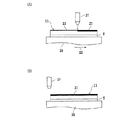
アライメント実施後、集光器37を図8(A)に示すように、レーザー加工すべき分割予定ライン13の端部の真上に位置付け、積層体21に対して吸収性を有する波長(例えば355nm)のビーム径の拡大された第1のパルスレーザービームLB1を集光器37で集光して、第1の方向に伸長する分割予定ライン13に沿って照射しつつ、図8(B)に示すように、チャックテーブル28を矢印X1方向に所定の加工送り速度で移動させて図10(B)に示す膜剥がれ防止溝23を形成する。そして、図8(B)に示すように、分割予定ライン13の他端部でレーザービームの照射を停止するとともにチャックテーブル28の加工送りを停止する。
After the alignment, as shown in FIG. 8 (A), the
膜剥がれ防止溝形成ステップでの第1のパルスレーザービームLB1は、図5(A)に示すようなガウシアン分布のエネルギー強度分布を有しているため、スリット領域87Aの両端部でも比較的高いエネルギーP1のレーザービームを積層体21に照射できるため、図10(B)に示すように、積層体21を分断する幅の広い膜剥がれ防止溝23を分割予定ライン13に沿って形成することができる。
Since the first pulse laser beam LB1 in the film peeling prevention groove forming step has a Gaussian distribution energy intensity distribution as shown in FIG. 5A, a relatively high energy is also obtained at both ends of the
図5(A)を参照すると明らかなように、照射される第1のパルスレーザービームLB1は中央部分のエネルギー量の方が両端部分よりも高いが、TEG17が加工しにくいため膜剥がれ防止溝23は符号25に示す中央部分で浅くしか形成できない。この膜剥がれ防止溝23の幅は、分割予定ライン13の幅よりも狭く且つ後で使用する切削ブレードの切刃の幅(例えば30μm)より広い幅を有している。
As apparent from FIG. 5A, the irradiated first pulse laser beam LB1 has a higher energy amount at the center than at both ends, but the
一本の分割予定ライン13について膜剥がれ防止溝23の形成が終了すると、同一の分割予定ライン13についてチャックテーブル28を逆方向に加工送りしながら、TEG17を除去するTEG除去用溝形成ステップを実施する。
When the formation of the film
このTEG除去用溝形成ステップでは、1/2波長板70を45度回転して、レーザービーム発生ユニット35から出射されるパルスレーザービームLBの偏光面を90度回転してS偏光に変換する。
In this TEG removal groove forming step, the half-
これにより、S偏光のパルスレーザービームLBは偏光ビームスプリッター72で反射されて、第2のパルスレーザービームLB2として第2の光路74bに導かれ、第2ビーム径調整手段82によりビーム径が縮小されて、図5(B)に示すような、急峻なガウシアン分布のエネルギー強度分布となる。
As a result, the S-polarized pulse laser beam LB is reflected by the
よって、第2のパルスレーザービームLB2を集光器37で集光して分割予定ライン13に沿って照射しつつ、図9(A)に示すように、チャックテーブル28を矢印X2方向に加工送りして、図10(C)に示すような、TEG除去用溝27を形成するTEG除去用溝形成ステップを実施する。
Therefore, the second pulse laser beam LB2 is condensed by the
図9(B)に示すように、集光器37が分割予定ライン13の一端部直上まできたらレーザービームの照射を停止するとともに、チャックテーブル28の加工送りを停止する。次いで、チャックテーブル28をY軸方向に分割予定ライン13の1ピッチ移動して隣の分割予定ライン13に集光器37を位置付け、図8に示す膜剥がれ防止溝形成ステップと、図9に示すTEG除去用溝形成ステップをその分割予定ライン13について繰り返す。
As shown in FIG. 9B, when the
チャックテーブル28を分割予定ライン13のピッチずつY軸方向に割り出し送りしながら、第1の方向に伸長する全ての分割予定ライン13に沿って同様な膜剥がれ防止溝23及びTEG除去用溝27を形成する。
While the chuck table 28 is indexed and fed in the Y-axis direction by the pitch of the
次いで、チャックテーブル28を90度回転してから、第1の方向と直交する第2の方向に伸長する全ての分割予定ライン13に沿って同様な膜剥がれ防止溝23及びTEG除去用溝27を形成する。
Next, after the chuck table 28 is rotated by 90 degrees, the same film peeling
本実施形態のウエーハのレーザー加工方法でのレーザー加工条件は例えば以下のように設定される。 The laser processing conditions in the wafer laser processing method of the present embodiment are set as follows, for example.
光源 :YAGパルスレーザ又はYVO4パルスレーザ
波長 :355nm
平均出力 :7〜10W
繰り返し周波数 :100〜130kHz
加工送り速度 :70〜100mm/s
Light source: YAG pulse laser or YVO4 pulse laser Wavelength: 355 nm
Average output: 7-10W
Repetition frequency: 100 to 130 kHz
Processing feed rate: 70 to 100 mm / s
上述した実施形態では、膜剥がれ防止溝形成ステップを実施した後TEG除去用溝形成ステップを実施しているが、TEG除去用溝形成ステップを先に実施し、その後に膜剥がれ防止溝形成ステップを実施するようにしてもよい。 In the above-described embodiment, the TEG removal groove forming step is performed after the film peeling prevention groove forming step is performed. However, the TEG removal groove forming step is performed first, and then the film peeling prevention groove forming step is performed. You may make it implement.
また、上述した実施形態では、一本の分割予定ライン13について加工送りの往路で膜剥がれ防止溝形成ステップを実施し、復路でTEG除去用溝形成ステップを実施しているが、本発明のレーザー加工方法がこれに限定されるものではない。
Further, in the above-described embodiment, the film peeling prevention groove forming step is performed in the processing feed forward path and the TEG removal groove forming step is performed in the backward path for one division planned
例えば、膜剥がれ防止溝形成ステップを第1の方向に伸長する全ての分割予定ライン13に沿って実施した後、第1の方向に伸長する全ての分割予定ライン13に沿ってTEG除去用溝形成ステップを実施し、次いでチャックテーブル28を90度回転してから、第2の方向に伸長する全ての分割予定ライン13に沿って膜剥がれ防止溝形成ステップを実施し、その後第2の方向に伸長する全ての分割予定ライン13に沿ってTEG除去用溝形成ステップを実施してもよい。
For example, after the film peeling prevention groove forming step is performed along all the
他の実施形態として、第1の方向に伸長する全ての分割予定ライン13及び第2の方向に伸長する全ての分割予定ライン13に沿って膜剥がれ防止溝形成ステップを実施した後、第1の方向に伸長する全ての分割予定ライン13及び第2の方向に伸長する全ての分割予定ライン13に沿ってTEG除去用溝形成ステップを実施してもよい。 As another embodiment, after performing the film peeling prevention groove forming step along all the division lines 13 extending in the first direction and all the division lines 13 extending in the second direction, The TEG removal groove forming step may be performed along all the division lines 13 extending in the direction and all the division lines 13 extending in the second direction.
膜剥がれ防止溝形成ステップ及びTEG除去用溝形成ステップを実施した後、切削装置の切削ブレードにより分割予定ライン13を切削して半導体ウエーハ11を個々の半導体デバイス15に分割する。
After performing the film peeling preventing groove forming step and the TEG removing groove forming step, the dividing
上述した実施形態では、本発明のレーザー加工方法をLow−k膜及びTEGを有する半導体ウエーハ11について実施した例について説明したが、ウエーハは半導体ウエーハに限定されるものではなく、層間絶縁膜として同様なLow−k膜を使用し、更に分割予定ライン上にTEGを有する光デバイスウエーハ等の他のウエーハにも、本発明のレーザー加工方法は同様に適用することができる。
In the above-described embodiment, the example in which the laser processing method of the present invention is applied to the
2 レーザー加工装置
11 半導体ウエーハ
13 分割予定ライン
15 半導体デバイス
17 TEG
19 シリコン基板
21 積層体
23 膜剥がれ防止溝
27 TEG除去用溝
34 レーザービーム照射ユニット
35 レーザービーム発生ユニット
37 集光器
62 レーザー発振器
70 1/2波長板
72,80 偏光ビームスプリッター
76,84 ミラー
78 第1ビーム径調整手段
82 第2ビーム径調整手段
86 マスク
87 スリット
88 結像用補助レンズ
90 集光レンズ
2
19
Claims (1)
該分割予定ラインの幅方向に対して所定の幅で溝が形成されるように、第1のビーム径を有する第1レーザービームを通過範囲を規制するマスクを介して、該分割予定ラインに沿って照射して、該分割予定ラインに1条の膜剥がれ防止溝を形成する膜剥がれ防止溝形成ステップと、
該第1のビーム径より小さい第2のビーム径を有し該第1レーザービームのエネルギー量と同等のエネルギー量を有する第2レーザービームを、該マスクを介して該分割予定ラインに沿って照射して、該分割予定ラインに1条のTEG除去用溝を形成するTEG除去用溝形成ステップと、を備え、
該第1レーザービームはなだらかなガウシアン分布を有しており、該マスクを通過した該第1レーザービームの該分割予定ラインの幅方向両端部のエネルギー量は該膜剥がれ防止溝を形成するのに十分な第1のエネルギー量であり、
該第2レーザービームは該第1レーザービームに比較して急峻なガウシアン分布を有しており、該マスクを通過した該第2レーザービームの該分割予定ラインの幅方向両端部のエネルギー量は該第1のエネルギー量より低く、中央部分のエネルギー量は該第1のエネルギー量より高く該TEG除去用溝を形成するのに十分な第2のエネルギー量であることを特徴とするウエーハのレーザー加工方法。 A multilayer body including a low-dielectric-constant insulating film is laminated on the surface, and a plurality of planned division lines in which TEGs are formed in portions intersecting in a lattice shape by the multilayer body, and devices in each region partitioned by the planned division lines A wafer laser processing method for forming a laser processing groove by irradiating a wafer formed with a laser beam having an energy intensity distribution of Gaussian distribution along the division line.
The first laser beam having the first beam diameter is arranged along the planned division line through a mask that restricts the passage range of the first laser beam so that a groove is formed with a predetermined width with respect to the width direction of the planned division line. A film peeling prevention groove forming step for forming one film peeling prevention groove on the planned dividing line;
A second laser beam having a second beam diameter smaller than the first beam diameter and having an energy amount equivalent to the energy amount of the first laser beam is irradiated along the planned division line through the mask. And a TEG removal groove forming step of forming one TEG removal groove on the division planned line,
The first laser beam has a gentle Gaussian distribution, and the amount of energy at both ends in the width direction of the planned division line of the first laser beam that has passed through the mask is used to form the film peeling prevention groove. A sufficient first amount of energy,
The second laser beam has a steep Gaussian distribution compared to the first laser beam, and the energy amount at both ends in the width direction of the division line of the second laser beam that has passed through the mask is Laser processing of a wafer characterized in that the energy amount in the central portion is lower than the first energy amount and higher than the first energy amount and is a second energy amount sufficient to form the TEG removal groove. Method.
Priority Applications (1)
| Application Number | Priority Date | Filing Date | Title |
|---|---|---|---|
| JP2012059121A JP2013197108A (en) | 2012-03-15 | 2012-03-15 | Laser processing method for wafer |
Applications Claiming Priority (1)
| Application Number | Priority Date | Filing Date | Title |
|---|---|---|---|
| JP2012059121A JP2013197108A (en) | 2012-03-15 | 2012-03-15 | Laser processing method for wafer |
Publications (1)
| Publication Number | Publication Date |
|---|---|
| JP2013197108A true JP2013197108A (en) | 2013-09-30 |
Family
ID=49395758
Family Applications (1)
| Application Number | Title | Priority Date | Filing Date |
|---|---|---|---|
| JP2012059121A Pending JP2013197108A (en) | 2012-03-15 | 2012-03-15 | Laser processing method for wafer |
Country Status (1)
| Country | Link |
|---|---|
| JP (1) | JP2013197108A (en) |
Cited By (11)
| Publication number | Priority date | Publication date | Assignee | Title |
|---|---|---|---|---|
| JP2015154009A (en) * | 2014-02-18 | 2015-08-24 | 株式会社ディスコ | Detection method of laser beam-machined groove |
| JP2016034659A (en) * | 2014-08-04 | 2016-03-17 | 株式会社ディスコ | Laser processing device |
| KR20160040100A (en) * | 2014-10-02 | 2016-04-12 | 가부시기가이샤 디스코 | Wafer machining method |
| JP2017118096A (en) * | 2015-09-10 | 2017-06-29 | 株式会社ディスコ | Substrate processing method |
| KR20170112150A (en) * | 2016-03-31 | 2017-10-12 | 주식회사 엘지화학 | Laser beam machining device and Laser beam machining method |
| CN108994450A (en) * | 2017-06-07 | 2018-12-14 | 株式会社迪思科 | Laser processing and laser processing device |
| JP2019096884A (en) * | 2017-11-22 | 2019-06-20 | エーエスエム・テクノロジー・シンガポール・ピーティーイー・リミテッド | Laser-cutting using selective polarization |
| KR20200043917A (en) * | 2018-10-18 | 2020-04-28 | 에이에스엠 테크놀러지 싱가포르 피티이 엘티디 | Material cutting using laser pulses |
| CN114918558A (en) * | 2022-05-27 | 2022-08-19 | 武汉新芯集成电路制造有限公司 | Laser dicing apparatus and wafer dicing method |
| US11548096B2 (en) | 2018-06-20 | 2023-01-10 | Disco Corporation | Laser processing apparatus |
| WO2023145114A1 (en) * | 2022-01-28 | 2023-08-03 | 浜松ホトニクス株式会社 | Laser processing method and laser processing device |
Citations (3)
| Publication number | Priority date | Publication date | Assignee | Title |
|---|---|---|---|---|
| JP2005205469A (en) * | 2004-01-23 | 2005-08-04 | Sumitomo Heavy Ind Ltd | Laser beam machining apparatus and method |
| JP2008114239A (en) * | 2006-11-02 | 2008-05-22 | Disco Abrasive Syst Ltd | Laser beam machining apparatus |
| JP2009182019A (en) * | 2008-01-29 | 2009-08-13 | Disco Abrasive Syst Ltd | Wafer processing method |
-
2012
- 2012-03-15 JP JP2012059121A patent/JP2013197108A/en active Pending
Patent Citations (3)
| Publication number | Priority date | Publication date | Assignee | Title |
|---|---|---|---|---|
| JP2005205469A (en) * | 2004-01-23 | 2005-08-04 | Sumitomo Heavy Ind Ltd | Laser beam machining apparatus and method |
| JP2008114239A (en) * | 2006-11-02 | 2008-05-22 | Disco Abrasive Syst Ltd | Laser beam machining apparatus |
| JP2009182019A (en) * | 2008-01-29 | 2009-08-13 | Disco Abrasive Syst Ltd | Wafer processing method |
Cited By (17)
| Publication number | Priority date | Publication date | Assignee | Title |
|---|---|---|---|---|
| JP2015154009A (en) * | 2014-02-18 | 2015-08-24 | 株式会社ディスコ | Detection method of laser beam-machined groove |
| JP2016034659A (en) * | 2014-08-04 | 2016-03-17 | 株式会社ディスコ | Laser processing device |
| KR20160040100A (en) * | 2014-10-02 | 2016-04-12 | 가부시기가이샤 디스코 | Wafer machining method |
| KR102305375B1 (en) | 2014-10-02 | 2021-09-24 | 가부시기가이샤 디스코 | Wafer machining method |
| JP2017118096A (en) * | 2015-09-10 | 2017-06-29 | 株式会社ディスコ | Substrate processing method |
| KR20170112150A (en) * | 2016-03-31 | 2017-10-12 | 주식회사 엘지화학 | Laser beam machining device and Laser beam machining method |
| KR102202933B1 (en) * | 2016-03-31 | 2021-01-14 | 주식회사 엘지화학 | Laser beam machining device and Laser beam machining method |
| CN108994450A (en) * | 2017-06-07 | 2018-12-14 | 株式会社迪思科 | Laser processing and laser processing device |
| JP2018202468A (en) * | 2017-06-07 | 2018-12-27 | 株式会社ディスコ | Laser processing method and laser processing device |
| CN108994450B (en) * | 2017-06-07 | 2021-10-22 | 株式会社迪思科 | Laser processing method and laser processing apparatus |
| JP2019096884A (en) * | 2017-11-22 | 2019-06-20 | エーエスエム・テクノロジー・シンガポール・ピーティーイー・リミテッド | Laser-cutting using selective polarization |
| US11548096B2 (en) | 2018-06-20 | 2023-01-10 | Disco Corporation | Laser processing apparatus |
| KR20200043917A (en) * | 2018-10-18 | 2020-04-28 | 에이에스엠 테크놀러지 싱가포르 피티이 엘티디 | Material cutting using laser pulses |
| KR102356121B1 (en) * | 2018-10-18 | 2022-01-28 | 에이에스엠 테크놀러지 싱가포르 피티이 엘티디 | Material cutting using laser pulses |
| WO2023145114A1 (en) * | 2022-01-28 | 2023-08-03 | 浜松ホトニクス株式会社 | Laser processing method and laser processing device |
| CN114918558A (en) * | 2022-05-27 | 2022-08-19 | 武汉新芯集成电路制造有限公司 | Laser dicing apparatus and wafer dicing method |
| CN114918558B (en) * | 2022-05-27 | 2023-11-24 | 武汉新芯集成电路制造有限公司 | Laser dicing apparatus and wafer dicing method |
Similar Documents
| Publication | Publication Date | Title |
|---|---|---|
| JP2013197108A (en) | Laser processing method for wafer | |
| JP6022223B2 (en) | Laser processing equipment | |
| JP4694845B2 (en) | Wafer division method | |
| JP4422463B2 (en) | Semiconductor wafer dividing method | |
| JP5940906B2 (en) | Laser processing equipment | |
| JP2006187783A (en) | Laser beam machine | |
| JP2006032419A (en) | Laser processing method for wafer | |
| US20150303113A1 (en) | Wafer processing method | |
| JP6178077B2 (en) | Wafer processing method | |
| US9087914B2 (en) | Wafer processing method | |
| JP2008028113A (en) | Wafer machining method by laser | |
| TWI546860B (en) | And a method of ablating a substrate having a passivation film laminated | |
| JP2005209719A (en) | Method for machining semiconductor wafer | |
| JP2011156551A (en) | Laser beam machining device | |
| JP2004179302A (en) | Method for splitting semiconductor wafer | |
| JP2015167969A (en) | Laser processing device and laser processing method | |
| JP5536344B2 (en) | Laser processing equipment | |
| JP2010194584A (en) | Laser beam machining apparatus | |
| JP2005118832A (en) | Laser beam machining method and laser beam machining device | |
| JP5863264B2 (en) | Wafer processing method | |
| JP2016009757A (en) | Processing method of wafer and laser processing apparatus | |
| JP2015142015A (en) | Semiconductor wafer processing method | |
| JP6625852B2 (en) | Laser processing equipment | |
| JP5885454B2 (en) | Ablation processing method for substrate with passivation film laminated | |
| JP2013081957A (en) | Ablation method for passivation film-laminated substrate |
Legal Events
| Date | Code | Title | Description |
|---|---|---|---|
| A621 | Written request for application examination |
Free format text: JAPANESE INTERMEDIATE CODE: A621 Effective date: 20150213 |
|
| A977 | Report on retrieval |
Free format text: JAPANESE INTERMEDIATE CODE: A971007 Effective date: 20160218 |
|
| A131 | Notification of reasons for refusal |
Free format text: JAPANESE INTERMEDIATE CODE: A131 Effective date: 20160223 |
|
| A02 | Decision of refusal |
Free format text: JAPANESE INTERMEDIATE CODE: A02 Effective date: 20160823 |