JP2012120376A - Inverter device - Google Patents
Inverter device Download PDFInfo
- Publication number
- JP2012120376A JP2012120376A JP2010269500A JP2010269500A JP2012120376A JP 2012120376 A JP2012120376 A JP 2012120376A JP 2010269500 A JP2010269500 A JP 2010269500A JP 2010269500 A JP2010269500 A JP 2010269500A JP 2012120376 A JP2012120376 A JP 2012120376A
- Authority
- JP
- Japan
- Prior art keywords
- voltage
- smoothing capacitor
- charging circuit
- failure
- detection unit
- Prior art date
- Legal status (The legal status is an assumption and is not a legal conclusion. Google has not performed a legal analysis and makes no representation as to the accuracy of the status listed.)
- Granted
Links
- 238000001514 detection method Methods 0.000 claims abstract description 81
- 238000009499 grossing Methods 0.000 claims abstract description 57
- 239000003990 capacitor Substances 0.000 claims abstract description 53
- 238000006073 displacement reaction Methods 0.000 claims description 7
- 239000004065 semiconductor Substances 0.000 description 3
- 230000005856 abnormality Effects 0.000 description 2
- 238000010586 diagram Methods 0.000 description 2
- 238000000034 method Methods 0.000 description 2
- 230000002159 abnormal effect Effects 0.000 description 1
- 230000020169 heat generation Effects 0.000 description 1
Images


Abstract
Description
この発明は、直流電圧を平滑する平滑コンデンサと、この平滑された直流電圧を交流電圧に変換するインバータ部とを備えたインバータ装置において、平滑コンデンサを初期充電する充電回路の故障を検出する技術に関する。 The present invention relates to a technique for detecting a failure of a charging circuit that initially charges a smoothing capacitor in an inverter device including a smoothing capacitor that smoothes a DC voltage and an inverter unit that converts the smoothed DC voltage into an AC voltage. .
一般にインバータ装置においては、直流中間部に平滑コンデンサを備えている。このようなインバータ装置の起動時には、交流電源の交流電圧をコンバータ部により整流して平滑コンデンサを充電するが、電源投入直後は平滑コンデンサに電荷が充電されていないので大きな突入電流が流れる。この初期充電時の突入電流を抑制するために、抵抗器とこの抵抗器の両端を短絡するリレー等の接点要素とからなる充電回路を設けている。 In general, an inverter device includes a smoothing capacitor in a direct current intermediate portion. At the time of starting such an inverter device, the AC voltage of the AC power supply is rectified by the converter unit to charge the smoothing capacitor. However, immediately after the power is turned on, the smoothing capacitor is not charged, so a large inrush current flows. In order to suppress the inrush current during the initial charging, a charging circuit including a resistor and a contact element such as a relay that short-circuits both ends of the resistor is provided.
この充電回路の異常を検出するものとして、例えば特許文献1に示すものがある。この特許文献1には、抵抗器の通流状態を検出する通流検出器を設け、抵抗器への通流状態があらかじめ定められた充電時間を超えて一定時間以上継続する場合には充電回路の故障と判断して異常表示を行うことが記載されている。
For example, Japanese Patent Application Laid-Open No. H10-228707 discloses a method for detecting an abnormality in the charging circuit. In this
上記特許文献1では、充電回路の故障検出を行うために抵抗器の通流状態を検出する電流検出器等の通流検出器が必要であり、インバータ装置が大型化するとともに、コストアップになるという問題があった。
In
この発明の目的は、特別な検出器等を設けることなく、平滑コンデンサの耐圧保護などを目的として一般に設けられている既設の電圧検出器を用いて充電回路の故障検出を容易に実現することができるインバータ装置を提供することを目的とする。 An object of the present invention is to easily realize fault detection of a charging circuit using an existing voltage detector that is generally provided for the purpose of protecting a smoothing capacitor withstand voltage without providing a special detector or the like. An object of the present invention is to provide an inverter device that can be used.
上記目的を達成するために、この発明は、直流電圧を平滑する平滑コンデンサと、該平滑コンデンサにより平滑された直流電圧を交流電圧に変換するインバータ部と、抵抗器と接点要素との並列回路から構成され前記平滑コンデンサを初期充電する充電回路と、前記平滑コンデンサの両端電圧を検出する電圧検出部とを備えたインバータ装置において、前記電圧検出部で検出された電圧に基づき、所定期間内における前記電圧の変位量から前記接点要素の短絡故障または/および開放故障を検出する充電回路故障検出部を備えるものとする。 In order to achieve the above object, the present invention comprises a smoothing capacitor for smoothing a DC voltage, an inverter unit for converting the DC voltage smoothed by the smoothing capacitor into an AC voltage, and a parallel circuit of a resistor and a contact element. In an inverter device comprising a charging circuit configured to initially charge the smoothing capacitor and a voltage detection unit that detects a voltage across the smoothing capacitor, based on the voltage detected by the voltage detection unit, the predetermined period of time A charging circuit failure detection unit that detects a short-circuit failure or / and an open failure of the contact element from a voltage displacement amount is provided.
この発明によれば、抵抗器と接点要素との並列回路から構成され平滑コンデンサを初期充電する充電回路と、平滑コンデンサの両端電圧を検出する電圧検出部と、この電圧検出部で検出された電圧に基づき、所定期間内における前記電圧の変位量から接点要素の短絡故障あるいは開放故障を検出する充電回路故障検出部とを備えることにより、特別な検出器等を設けることなく、簡易な構成により充電回路の故障検出を行うことができる。 According to the present invention, a charging circuit configured by a parallel circuit of a resistor and a contact element for initially charging a smoothing capacitor, a voltage detection unit for detecting a voltage across the smoothing capacitor, and a voltage detected by the voltage detection unit And a charging circuit failure detection unit that detects a short-circuit failure or an open-circuit failure of the contact element from the amount of displacement of the voltage within a predetermined period, thereby charging with a simple configuration without providing a special detector or the like. Circuit failure detection can be performed.
図1はこの発明の実施の形態を示すインバータ装置の回路構成図である。図1において、1は三相の商用交流電源、2はインバータ装置10の入力側に設けられた遮断器、3はインバータ装置10により駆動される電動機である。
FIG. 1 is a circuit configuration diagram of an inverter device showing an embodiment of the present invention. In FIG. 1, 1 is a three-phase commercial AC power source, 2 is a circuit breaker provided on the input side of the
また、11は交流電圧を三相全波整流するコンバータ部であり、ダイオードを三相ブリッジ接続したものである。12は直流母線間に接続されてコンバータ部11の出力を平滑する平滑コンデンサであり、通常は電解コンデンサが用いられている。13は平滑コンデンサ12の両端の平滑された直流電圧を入力として所望の周波数と電圧とをもつ交流電圧に変換するインバータ部であり、IGBT等の半導体スイッチング素子と還流用ダイオードとの逆並列回路を三相ブリッジ接続したものである。これらコンバータ部11,平滑コンデンサ12,インバータ部13によりインバータ装置10の主回路が構成されている。14はコンバータ部11と平滑コンデンサ12との間に接続されて初期充電電流を限流するための抵抗器、15は抵抗器14に並列に接続されて抵抗器14の両端を短絡するリレー等の接点要素であり、この抵抗器14および接点要素15により平滑コンデンサ12を初期充電するための充電回路16を構成している。
17は平滑コンデンサ12の両端の直流電圧を検出する電圧検出部であり、検出した電圧検出値を電圧検出信号として送出する。なお、電圧検出部17は平滑コンデンサ12の耐圧保護などを目的としてインバータ装置10に一般的に設けられているものである。18は電圧検出部17からの電圧検出信号に基づいて所定期間の電圧上昇の傾きを演算し、この傾きから接点要素15の開放故障あるいは短絡故障を判定する充電回路故障検出部である。この充電回路故障検出部18は接点要素14を開閉するための接点信号を出力し、また接点要素14の故障と判定した際に故障検出信号を出力する。19はインバータ制御部であり、不図示の周波数設定器からの周波数指令値に基づいて電圧指令信号を演算し、この電圧指令信号とキャリア周波数信号との比較によるPWM演算を行ってインバータ部13を構成する各半導体スイッチング素子をオン・オフ制御するためのPWM信号を生成する。20は充電回路故障検出部18が故障を検出した際の故障表示を行う表示部である。
このような構成において、図2を参照しながら充電回路16が正常時の初期充電動作を説明する。
In such a configuration, an initial charging operation when the
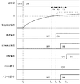
インバータ装置10を起動する際、時刻t0において遮断器2が閉路されて商用交流電源1が投入されると、交流電圧がコンバータ部11により整流されて平滑コンデンサ12の初期充電が開始される。このとき接点要素15は開放されているので、平滑コンデンサ12には抵抗器14を介して抑制された充電電流が流れ、抵抗器14と平滑コンデンサ12の時定数で決まる時間で平滑コンデンサ12の電圧が上昇する。
When starting the
次に、時刻t1において平滑コンデンサ12の両端電圧が所定の電圧V1(例えば、初期充電完了後のピーク充電電圧の80%程度にあらかじめ設定した値)に達すると、あらかじめ定めた所定時間T1が経過した後の時刻t2における電圧を電圧検出部17で検出し、充電回路故障検出部18により時刻t1での電圧検出信号に基づく電圧検出値と時刻t2での電圧検出信号に基づく電圧検出値とから時刻t1−t2間の電圧上昇の傾きを演算する。この演算した傾きがあらかじめ設定されている第1の基準値未満のときは充電回路16が正常と判断(接点要素15が短絡故障していないと判断)するとともに、接点信号をONにして接点要素15を閉路して抵抗器14を短絡することによって平滑コンデンサ12を完全に充電する。このとき充電回路故障検出部18からの故障検出信号はOFFのままである。
Next, when the voltage across the
次に、充電回路故障検出部18では、時刻t2からあらかじめ定めた所定時間T2が経過した後の時刻t3において時刻t2−t3間の電圧上昇の傾きを時刻t2およびt3での電圧検出信号に基づいて演算する。この演算した傾きがあらかじめ設定した第2の基準値以上のときは充電回路16が正常と判断(接点要素15が開放故障していないと判断)する。このときも充電回路故障検出部18からの故障検出信号はOFFのままである。なお、上述の第1の基準値と第2の基準値は同じ値にしてもよいし、それぞれ別の値にしてもよい。
Next, the charging circuit
その後、あらかじめ定めた所定時間T3が経過した後の時刻t4において運転信号がOFFからONになるが、このときの故障検出信号はOFFであるので、PWM信号がONになる。インバータ制御部19ではPWM信号を生成し、このPWM信号に従ってインバータ部13を構成する各半導体スイッチング素子をオン・オフ制御することにより、インバータ装置10の出力電圧がその指令値に一致するような制御が行われる。
Thereafter, the operation signal is turned from OFF to ON at time t4 after a predetermined time T3 elapses in advance. Since the failure detection signal at this time is OFF, the PWM signal is turned ON. The
次に、図3を参照しながら充電回路16が故障時(接点要素15の短絡故障時)の動作を説明する。
Next, the operation when the
時刻t0において遮断器2が閉路され商用交流電源1が投入されると、コンバータ部11を介して平滑コンデンサ12の初期充電が開始される。ここで接点要素15が溶着するなどして短絡故障している場合、遮断器2を閉路すると平滑コンデンサ12の両端電圧が急峻に上昇する。
When the
次に、時刻t11において平滑コンデンサ12の両端電圧が所定の電圧V1に達すると、あらかじめ定めた所定時間T1が経過した後の時刻t12での電圧を電圧検出部17で検出し、充電回路故障検出部18により時刻t11の電圧検出信号に基づく電圧検出値と時刻t12の電圧検出信号に基づく電圧検出値とから時刻t11−t12間の電圧上昇の傾きを演算する。この演算した傾きが第1の基準値以上のときは充電回路16の故障と判断(接点要素15が短絡故障と判断)し、故障検出信号をインバータ制御回路19に出力する。そしてインバータ制御回路19からアラーム信号を出力し、表示部20に充電回路16の故障を表示する。
Next, when the voltage between both ends of the
その後、時刻t14において運転信号がOFFからONになるが、充電回路故障検出部18からの故障検出信号がONのため、PWM信号はOFFとなりインバータ装置10を停止する。
Thereafter, the operation signal is turned from OFF to ON at time t14. However, since the failure detection signal from the charging circuit
なお、故障判定の精度を向上させるために、時刻t12で接点信号をONにし、この時刻t12の前後の電圧検出信号の値から電圧上昇の傾きを充電回路故障検出部18で演算し、この演算した傾きから充電回路16の故障を判断するシーケンスを追加するようにしてもよい。このとき、電圧上昇の傾きに変化がなければ充電回路16の短絡故障と判断し、電圧上昇の傾きに変化があれば充電回路16が正常と判断する。
In order to improve the accuracy of the failure determination, the contact signal is turned on at time t12, and the charging circuit
また、充電回路故障検出部18が充電回路16の短絡故障と判断した場合、遮断器信号に基づいて遮断器2を開路する機能を備えることによって、より安全にインバータ装置10の保護を行うことができる。
Further, when the charging circuit
次に、図4を参照しながら充電回路16が故障時(接点要素15の開放故障時)の動作を説明する。
Next, the operation when the charging
時刻t0において遮断器2が閉路され商用交流電源1が投入されると、コンバータ部11を介して平滑コンデンサ12の初期充電が開始される。このとき接点要素15は開放されており、抵抗器14と平滑コンデンサ12の時定数で決まる時間で平滑コンデンサ12の両端電圧が上昇する。
When the
次に、時刻t21において平滑コンデンサ12の両端電圧が所定の電圧V1に達すると、あらかじめ定めた所定時間T1が経過した後の時刻t22での電圧を電圧検出部17で検出し、充電回路故障検出部18により時刻t21の電圧検出信号に基づく電圧検出値と時刻t22の電圧検出信号に基づく電圧検出値とから時刻t21−t22間の電圧上昇の傾きを演算する。この演算した傾きが第1の基準値未満のときは充電回路16が正常と判断(接点要素15が短絡故障していないと判断)し、接点信号をONにする。このとき充電回路故障検出部18からの故障検出信号はOFFのままである。
Next, when the voltage between both ends of the smoothing
ここで何らかの原因で接点要素15が開放したまま閉路できない故障が発生した場合、抵抗器14の両端が短絡できないために抵抗器14に電流が流れ続け、平滑コンデンサ12の両端電圧は時刻t22以前と同様に抵抗器14と平滑コンデンサ12の時定数で決まる時間でゆっくりと上昇する。次に、あらかじめ定めた所定時間T2が経過した後の時刻t23において、時刻t22およびt23での電圧検出信号に基づいて時刻t22−t23間の電圧上昇の傾きを充電回路故障検出部18で演算する。この演算した傾きが第2の基準値未満のときは充電回路16が故障と判断(接点要素15が開放故障と判断)し、充電回路故障検出部18がインバータ制御回路19に故障検出信号を出力する。そしてインバータ制御回路19からアラーム信号を出力し、表示部20に充電回路16の故障を表示する。
Here, when a failure that cannot be closed with the
その後、時刻t24において運転信号がOFFからONになるが、充電回路故障検出部18からの故障検出信号がONのため、PWM信号はOFFとなりインバータ装置10を停止する。
Thereafter, the operation signal is switched from OFF to ON at time t24. However, since the failure detection signal from the charging circuit
なお、充電回路故障検出部18が充電回路16の開放故障と判断した場合、遮断器信号により遮断器2を開路する機能を備えることによって、より安全にインバータ装置10の保護を行うことができる。
When the charging circuit
また、上記実施の形態においては、所定期間内における前記電圧の変位量として、所定期間内の電圧上昇の傾きを演算して充電回路の故障を判断するようにしているが、所定期間内の電圧上昇値(偏差)から充電回路の故障を判断するようにしてもよい。 Further, in the above embodiment, as the amount of displacement of the voltage within a predetermined period, the slope of the voltage rise within the predetermined period is calculated to determine the failure of the charging circuit. A failure of the charging circuit may be determined from the increased value (deviation).
以上のように、本発明によれば、平滑コンデンサ12の初期充電時に電圧検出部17で検出された電圧検出信号に基づく電圧検出値の所定期間内における電圧の変位量から接点要素15の短絡故障あるいは開放故障を検出する充電回路故障検出部18を備えることにより、平滑コンデンサ12の耐圧保護などを目的として一般に設けられている既設の電圧検出部17のみを用いて充電回路16の故障の検出を容易に実現し、抵抗器14の異常発熱による焼損等の二次故障を防止することができる。
As described above, according to the present invention, the short-circuit failure of the
10…インバータ装置、11…コンバータ部、12…平滑コンデンサ、13…インバータ部、14…抵抗器、15…接点要素、16…充電回路、17…電圧検出部、18…充電回路故障検出部、19…インバータ制御部、20…表示部。
DESCRIPTION OF
Claims (5)
前記電圧検出部で検出された電圧に基づき、所定期間内における前記電圧の変位量から前記接点要素の短絡故障を検出する充電回路故障検出部を備えたことを特徴とするインバータ装置。 A smoothing capacitor for smoothing the DC voltage, an inverter unit for converting the DC voltage smoothed by the smoothing capacitor into an AC voltage, and a charging circuit for initially charging the smoothing capacitor, comprising a parallel circuit of a resistor and a contact element; In the inverter device comprising a voltage detection unit for detecting the voltage across the smoothing capacitor,
An inverter device comprising: a charging circuit failure detection unit that detects a short-circuit failure of the contact element from a displacement amount of the voltage within a predetermined period based on a voltage detected by the voltage detection unit.
前記電圧検出部で検出された電圧に基づき、所定期間内における前記電圧の変位量から前記接点要素の開放故障を検出する充電回路故障検出部を備えたことを特徴とするインバータ装置。 A smoothing capacitor for smoothing the DC voltage, an inverter unit for converting the DC voltage smoothed by the smoothing capacitor into an AC voltage, and a charging circuit for initially charging the smoothing capacitor, comprising a parallel circuit of a resistor and a contact element; In the inverter device comprising a voltage detection unit for detecting the voltage across the smoothing capacitor,
An inverter device comprising: a charging circuit failure detection unit that detects an open failure of the contact element from a displacement amount of the voltage within a predetermined period based on a voltage detected by the voltage detection unit.
前記電圧検出部で検出された電圧に基づき、所定期間内における前記電圧の変位量から前記接点要素の開放故障および短絡故障を検出する充電回路故障検出部を備えたことを特徴とするインバータ装置。 A smoothing capacitor for smoothing the DC voltage, an inverter unit for converting the DC voltage smoothed by the smoothing capacitor into an AC voltage, and a charging circuit for initially charging the smoothing capacitor, comprising a parallel circuit of a resistor and a contact element; In the inverter device comprising a voltage detection unit for detecting the voltage across the smoothing capacitor,
An inverter device comprising: a charging circuit failure detection unit that detects an open failure and a short-circuit failure of the contact element from a displacement amount of the voltage within a predetermined period based on a voltage detected by the voltage detection unit.
Priority Applications (1)
| Application Number | Priority Date | Filing Date | Title |
|---|---|---|---|
| JP2010269500A JP5728914B2 (en) | 2010-12-02 | 2010-12-02 | Inverter device |
Applications Claiming Priority (1)
| Application Number | Priority Date | Filing Date | Title |
|---|---|---|---|
| JP2010269500A JP5728914B2 (en) | 2010-12-02 | 2010-12-02 | Inverter device |
Publications (2)
| Publication Number | Publication Date |
|---|---|
| JP2012120376A true JP2012120376A (en) | 2012-06-21 |
| JP5728914B2 JP5728914B2 (en) | 2015-06-03 |
Family
ID=46502572
Family Applications (1)
| Application Number | Title | Priority Date | Filing Date |
|---|---|---|---|
| JP2010269500A Active JP5728914B2 (en) | 2010-12-02 | 2010-12-02 | Inverter device |
Country Status (1)
| Country | Link |
|---|---|
| JP (1) | JP5728914B2 (en) |
Cited By (12)
| Publication number | Priority date | Publication date | Assignee | Title |
|---|---|---|---|---|
| JP5820021B1 (en) * | 2014-06-13 | 2015-11-24 | ファナック株式会社 | Motor control device having charging resistance protection means |
| JP2017200421A (en) * | 2016-04-26 | 2017-11-02 | エルエス産電株式会社Lsis Co., Ltd. | Operation control device of power converting device |
| JP2017200418A (en) * | 2016-04-27 | 2017-11-02 | エルエス産電株式会社Lsis Co., Ltd. | Malfunction detector of relay |
| JP6279192B1 (en) * | 2017-07-28 | 2018-02-14 | 三菱電機株式会社 | Inverter device and abnormality detection method for inverter device |
| JP2018057070A (en) * | 2016-09-26 | 2018-04-05 | 三洋電機株式会社 | Power supply system |
| KR20180101752A (en) * | 2017-03-06 | 2018-09-14 | 엘에스산전 주식회사 | Device detecting fault of inverter power relay |
| EP3531543A1 (en) * | 2018-02-26 | 2019-08-28 | LSIS Co., Ltd. | Device and method for controlling an inverter |
| JP2021019377A (en) * | 2019-07-17 | 2021-02-15 | ファナック株式会社 | Power conversion device and control method therefor |
| JP2021087306A (en) * | 2019-11-28 | 2021-06-03 | ファナック株式会社 | rectifier |
| WO2021172736A1 (en) * | 2020-02-24 | 2021-09-02 | 엘에스일렉트릭 주식회사 | Device and method for diagnosing failure of inverter initial charging circuit |
| CN114113994A (en) * | 2020-08-28 | 2022-03-01 | 台达电子工业股份有限公司 | Power switch fault detection method and detection circuit thereof |
| TWI757851B (en) * | 2020-08-28 | 2022-03-11 | 台達電子工業股份有限公司 | Power switch fault detection method for brake circuit and circuit of detectiing the same |
Citations (8)
| Publication number | Priority date | Publication date | Assignee | Title |
|---|---|---|---|---|
| JPH07308020A (en) * | 1994-05-10 | 1995-11-21 | Hitachi Ltd | Air-conditioner |
| JPH10201004A (en) * | 1997-01-08 | 1998-07-31 | Toshiba Corp | Power supply for car |
| JPH10225134A (en) * | 1997-02-06 | 1998-08-21 | Fujitec Co Ltd | Abnormality detecting circuit for inverter |
| JP2000134707A (en) * | 1998-10-26 | 2000-05-12 | Toyota Motor Corp | Power supply controller |
| JP2005276565A (en) * | 2004-03-24 | 2005-10-06 | Toyota Motor Corp | Power supply control device and determining method of welding in power supply control device |
| JP2007059138A (en) * | 2005-07-25 | 2007-03-08 | Toyota Motor Corp | Power supply controller |
| JP2007060855A (en) * | 2005-08-26 | 2007-03-08 | Matsushita Electric Ind Co Ltd | Air conditioning device |
| JP2007250335A (en) * | 2006-03-15 | 2007-09-27 | Toyota Motor Corp | Power supply control device |
-
2010
- 2010-12-02 JP JP2010269500A patent/JP5728914B2/en active Active
Patent Citations (8)
| Publication number | Priority date | Publication date | Assignee | Title |
|---|---|---|---|---|
| JPH07308020A (en) * | 1994-05-10 | 1995-11-21 | Hitachi Ltd | Air-conditioner |
| JPH10201004A (en) * | 1997-01-08 | 1998-07-31 | Toshiba Corp | Power supply for car |
| JPH10225134A (en) * | 1997-02-06 | 1998-08-21 | Fujitec Co Ltd | Abnormality detecting circuit for inverter |
| JP2000134707A (en) * | 1998-10-26 | 2000-05-12 | Toyota Motor Corp | Power supply controller |
| JP2005276565A (en) * | 2004-03-24 | 2005-10-06 | Toyota Motor Corp | Power supply control device and determining method of welding in power supply control device |
| JP2007059138A (en) * | 2005-07-25 | 2007-03-08 | Toyota Motor Corp | Power supply controller |
| JP2007060855A (en) * | 2005-08-26 | 2007-03-08 | Matsushita Electric Ind Co Ltd | Air conditioning device |
| JP2007250335A (en) * | 2006-03-15 | 2007-09-27 | Toyota Motor Corp | Power supply control device |
Cited By (32)
| Publication number | Priority date | Publication date | Assignee | Title |
|---|---|---|---|---|
| JP2016005317A (en) * | 2014-06-13 | 2016-01-12 | ファナック株式会社 | Motor controller with protection means for charging resistor |
| CN105281643A (en) * | 2014-06-13 | 2016-01-27 | 发那科株式会社 | Motor control device |
| US9444373B2 (en) | 2014-06-13 | 2016-09-13 | Fanuc Corporation | Motor control device having protective unit of charging resistor |
| JP5820021B1 (en) * | 2014-06-13 | 2015-11-24 | ファナック株式会社 | Motor control device having charging resistance protection means |
| KR102526874B1 (en) * | 2016-04-26 | 2023-04-27 | 엘에스일렉트릭(주) | Apparatus for controlling operation of power conversion device |
| JP2017200421A (en) * | 2016-04-26 | 2017-11-02 | エルエス産電株式会社Lsis Co., Ltd. | Operation control device of power converting device |
| US10003296B2 (en) | 2016-04-26 | 2018-06-19 | Lsis Co., Ltd. | Apparatus for controlling operation of power conversion device and monitoring operation state of relay |
| KR20170122057A (en) * | 2016-04-26 | 2017-11-03 | 엘에스산전 주식회사 | Apparatus for controlling operation of power conversion device |
| CN107315141A (en) * | 2016-04-27 | 2017-11-03 | Ls 产电株式会社 | For the equipment for the failure for detecting relay |
| US20170317487A1 (en) * | 2016-04-27 | 2017-11-02 | Lsis Co., Ltd. | Apparatus for detecting malfunction of relay |
| US10020648B2 (en) | 2016-04-27 | 2018-07-10 | Lsis Co., Ltd. | Apparatus for detecting malfunction of relay |
| JP2017200418A (en) * | 2016-04-27 | 2017-11-02 | エルエス産電株式会社Lsis Co., Ltd. | Malfunction detector of relay |
| JP2018057070A (en) * | 2016-09-26 | 2018-04-05 | 三洋電機株式会社 | Power supply system |
| US10594129B2 (en) | 2017-03-06 | 2020-03-17 | Lsis Co., Ltd. | Apparatus for detecting fault of power relay of inverter |
| KR20180101752A (en) * | 2017-03-06 | 2018-09-14 | 엘에스산전 주식회사 | Device detecting fault of inverter power relay |
| CN108535637A (en) * | 2017-03-06 | 2018-09-14 | Ls产电株式会社 | The equipment of the failure of power relay for detecting inverter |
| JP2018148777A (en) * | 2017-03-06 | 2018-09-20 | エルエス産電株式会社Lsis Co., Ltd. | Power relay failure-sensing device of invertor |
| KR102307999B1 (en) | 2017-03-06 | 2021-09-30 | 엘에스일렉트릭(주) | Device detecting fault of inverter power relay |
| WO2019021479A1 (en) * | 2017-07-28 | 2019-01-31 | 三菱電機株式会社 | Inverter device and inverter device abnormality detection method |
| DE112017000303T5 (en) | 2017-07-28 | 2019-03-14 | Mitsubishi Electric Corporation | An inverter device and method for detecting an anomaly in an inverter device |
| JP6279192B1 (en) * | 2017-07-28 | 2018-02-14 | 三菱電機株式会社 | Inverter device and abnormality detection method for inverter device |
| JP2019149926A (en) * | 2018-02-26 | 2019-09-05 | エルエス産電株式会社Lsis Co., Ltd. | Inverter control device and control method thereof |
| US10566911B2 (en) | 2018-02-26 | 2020-02-18 | Lsis Co., Ltd. | Device and method for controlling inverter based on predetermined time durations and magnitude of the DC link voltage |
| EP3531543A1 (en) * | 2018-02-26 | 2019-08-28 | LSIS Co., Ltd. | Device and method for controlling an inverter |
| CN110198137A (en) * | 2018-02-26 | 2019-09-03 | Ls产电株式会社 | Control device for inverter and method |
| JP7244378B2 (en) | 2019-07-17 | 2023-03-22 | ファナック株式会社 | Power conversion device and its control method |
| JP2021019377A (en) * | 2019-07-17 | 2021-02-15 | ファナック株式会社 | Power conversion device and control method therefor |
| JP2021087306A (en) * | 2019-11-28 | 2021-06-03 | ファナック株式会社 | rectifier |
| WO2021172736A1 (en) * | 2020-02-24 | 2021-09-02 | 엘에스일렉트릭 주식회사 | Device and method for diagnosing failure of inverter initial charging circuit |
| TWI757851B (en) * | 2020-08-28 | 2022-03-11 | 台達電子工業股份有限公司 | Power switch fault detection method for brake circuit and circuit of detectiing the same |
| CN114113994A (en) * | 2020-08-28 | 2022-03-01 | 台达电子工业股份有限公司 | Power switch fault detection method and detection circuit thereof |
| US11644506B2 (en) | 2020-08-28 | 2023-05-09 | Delta Electronics, Inc. | Power switch fault detection method and power switch fault detection circuit |
Also Published As
| Publication number | Publication date |
|---|---|
| JP5728914B2 (en) | 2015-06-03 |
Similar Documents
| Publication | Publication Date | Title |
|---|---|---|
| JP5728914B2 (en) | Inverter device | |
| US9444373B2 (en) | Motor control device having protective unit of charging resistor | |
| JP6741169B2 (en) | Power supply device, power control device, power supply device relay determination method | |
| CN109601022B (en) | Inverter device and method for detecting abnormality of inverter device | |
| JP5689497B2 (en) | Motor drive device having DC link unit abnormality detection function | |
| WO2013001820A1 (en) | System connection inverter device and control method therefor | |
| US9581647B2 (en) | Motor drive having function of detecting welding of electromagnetic connector | |
| JP5095530B2 (en) | Abnormality determination method and abnormality determination device for charge / discharge system | |
| JP2007174792A (en) | System interconnection inverter device | |
| US20180294711A1 (en) | Converter apparatus having function of detecting failure of power device, and method for detecting failure of power device | |
| JP6133827B2 (en) | Motor driving device having welding detection function of magnetic contactor | |
| JP2018164377A (en) | Converter device with short-circuit fault detection function and short-circuit fault detection method for converter device | |
| WO2020241659A1 (en) | Converter device and industrial machine | |
| JP2016093018A (en) | Inverter control device | |
| JP6788489B2 (en) | Electric circuit and its control device | |
| JP5667915B2 (en) | DC power supply | |
| JP5008465B2 (en) | Uninterruptible power system | |
| US20220399746A1 (en) | Power converter | |
| JP6296878B2 (en) | Grid-connected inverter and generated power estimation method | |
| JP6886082B1 (en) | Power supply | |
| JP2015027146A (en) | Power conditioner | |
| JP2014217131A (en) | Electric power conversion system | |
| JP4962032B2 (en) | Control method of DC power supply system | |
| JP6782179B2 (en) | Vehicle-mounted inverter control method and control device | |
| KR101158414B1 (en) | Digital Battery Charger |
Legal Events
| Date | Code | Title | Description |
|---|---|---|---|
| A621 | Written request for application examination |
Free format text: JAPANESE INTERMEDIATE CODE: A621 Effective date: 20131011 |
|
| A977 | Report on retrieval |
Free format text: JAPANESE INTERMEDIATE CODE: A971007 Effective date: 20140722 |
|
| A131 | Notification of reasons for refusal |
Free format text: JAPANESE INTERMEDIATE CODE: A131 Effective date: 20140730 |
|
| A521 | Request for written amendment filed |
Free format text: JAPANESE INTERMEDIATE CODE: A523 Effective date: 20140909 |
|
| TRDD | Decision of grant or rejection written | ||
| A01 | Written decision to grant a patent or to grant a registration (utility model) |
Free format text: JAPANESE INTERMEDIATE CODE: A01 Effective date: 20150310 |
|
| A61 | First payment of annual fees (during grant procedure) |
Free format text: JAPANESE INTERMEDIATE CODE: A61 Effective date: 20150323 |
|
| R150 | Certificate of patent or registration of utility model |
Ref document number: 5728914 Country of ref document: JP Free format text: JAPANESE INTERMEDIATE CODE: R150 |
|
| R250 | Receipt of annual fees |
Free format text: JAPANESE INTERMEDIATE CODE: R250 |
|
| R250 | Receipt of annual fees |
Free format text: JAPANESE INTERMEDIATE CODE: R250 |
|
| R250 | Receipt of annual fees |
Free format text: JAPANESE INTERMEDIATE CODE: R250 |
|
| R250 | Receipt of annual fees |
Free format text: JAPANESE INTERMEDIATE CODE: R250 |
|
| R250 | Receipt of annual fees |
Free format text: JAPANESE INTERMEDIATE CODE: R250 |
|
| R250 | Receipt of annual fees |
Free format text: JAPANESE INTERMEDIATE CODE: R250 |
|
| R250 | Receipt of annual fees |
Free format text: JAPANESE INTERMEDIATE CODE: R250 |