JP2010516223A - Power converter with snubber - Google Patents
Power converter with snubber Download PDFInfo
- Publication number
- JP2010516223A JP2010516223A JP2009545044A JP2009545044A JP2010516223A JP 2010516223 A JP2010516223 A JP 2010516223A JP 2009545044 A JP2009545044 A JP 2009545044A JP 2009545044 A JP2009545044 A JP 2009545044A JP 2010516223 A JP2010516223 A JP 2010516223A
- Authority
- JP
- Japan
- Prior art keywords
- diode
- inductor
- series
- switch
- resistor
- Prior art date
- Legal status (The legal status is an assumption and is not a legal conclusion. Google has not performed a legal analysis and makes no representation as to the accuracy of the status listed.)
- Pending
Links
Images


Classifications
-
- H—ELECTRICITY
- H02—GENERATION; CONVERSION OR DISTRIBUTION OF ELECTRIC POWER
- H02M—APPARATUS FOR CONVERSION BETWEEN AC AND AC, BETWEEN AC AND DC, OR BETWEEN DC AND DC, AND FOR USE WITH MAINS OR SIMILAR POWER SUPPLY SYSTEMS; CONVERSION OF DC OR AC INPUT POWER INTO SURGE OUTPUT POWER; CONTROL OR REGULATION THEREOF
- H02M1/00—Details of apparatus for conversion
- H02M1/32—Means for protecting converters other than automatic disconnection
- H02M1/34—Snubber circuits
-
- H—ELECTRICITY
- H02—GENERATION; CONVERSION OR DISTRIBUTION OF ELECTRIC POWER
- H02M—APPARATUS FOR CONVERSION BETWEEN AC AND AC, BETWEEN AC AND DC, OR BETWEEN DC AND DC, AND FOR USE WITH MAINS OR SIMILAR POWER SUPPLY SYSTEMS; CONVERSION OF DC OR AC INPUT POWER INTO SURGE OUTPUT POWER; CONTROL OR REGULATION THEREOF
- H02M3/00—Conversion of dc power input into dc power output
- H02M3/02—Conversion of dc power input into dc power output without intermediate conversion into ac
- H02M3/04—Conversion of dc power input into dc power output without intermediate conversion into ac by static converters
- H02M3/10—Conversion of dc power input into dc power output without intermediate conversion into ac by static converters using discharge tubes with control electrode or semiconductor devices with control electrode
- H02M3/145—Conversion of dc power input into dc power output without intermediate conversion into ac by static converters using discharge tubes with control electrode or semiconductor devices with control electrode using devices of a triode or transistor type requiring continuous application of a control signal
- H02M3/155—Conversion of dc power input into dc power output without intermediate conversion into ac by static converters using discharge tubes with control electrode or semiconductor devices with control electrode using devices of a triode or transistor type requiring continuous application of a control signal using semiconductor devices only
Landscapes
- Engineering & Computer Science (AREA)
- Power Engineering (AREA)
- Dc-Dc Converters (AREA)
Abstract
第1のインダクタ(10)と、制御されたスイッチ(12)と、メインダイオード(14)と、出力キャパシタ(16)とを備える降圧または昇圧コンバータは、損失を減少させるためのスナバ回路を含む。スナバ回路は、コンバータのスイッチおよびメインダイオードと直列の経路に設けられた第2のインダクタ(20)と、第2のインダクタと並列に直接的に接続され、直列接続された抵抗(22)およびダイオード(24)と、メインダイオードと並列に設けられ、メインダイオードの寄生容量によってその一部または全部が構成されるキャパシタンス(28)とを含む。 A step-down or boost converter comprising a first inductor (10), a controlled switch (12), a main diode (14), and an output capacitor (16) includes a snubber circuit for reducing losses. The snubber circuit includes a second inductor (20) provided in a path in series with the switch and the main diode of the converter, and a resistor (22) and a diode connected directly in parallel with the second inductor. (24) and a capacitance (28) provided in parallel with the main diode and partially or entirely constituted by the parasitic capacitance of the main diode.
Description
本発明は、電力コンバータに関し、特定的には、追加のスイッチを必要としないスナバ回路を用いることにより損失が低減される電力コンバータに関する。 The present invention relates to a power converter, and more particularly to a power converter in which loss is reduced by using a snubber circuit that does not require an additional switch.
背景
従来の昇圧コンバータにおいては、入力電圧はインダクタを経由してスイッチ、典型的にはMOSFETに結合され、直列接続されたダイオードおよびキャパシタが、スイッチに並列に結合され、コンバータの出力電圧がキャパシタから引き出される。変圧器がない場合には、出力電圧は入力電圧より大きくなる。スイッチは、典型的には、制御されたデューティサイクルで、高周波数で交互に開閉される。
Background In a conventional boost converter, the input voltage is coupled via an inductor to a switch, typically a MOSFET, and a diode and capacitor connected in series are coupled in parallel to the switch so that the output voltage of the converter is derived from the capacitor. Pulled out. In the absence of a transformer, the output voltage will be greater than the input voltage. The switches are typically alternately opened and closed at a high frequency with a controlled duty cycle.
昇圧コンバータのさらに重要な用途は、民生用電子機器のための、いわゆるオフライン電源構成における、力率補正(power factor correction:PFC)である。このような構成においては、典型的には、整流された交流電源が、ほぼ1に近い力率を与えるために、昇圧コンバータによって高出力電圧に変換され、出力電圧は直接使用されたり、または、1つ以上の他の電力コンバータによって、使用のために、1つ以上の交流および/または直流電圧に変換されたりすることができる。 A further important application of the boost converter is power factor correction (PFC) in a so-called off-line power supply configuration for consumer electronics. In such a configuration, the rectified AC power supply is typically converted to a high output voltage by a boost converter to provide a power factor close to 1, and the output voltage is used directly, or One or more other power converters may be converted to one or more AC and / or DC voltages for use.
不連続電流モード(Discontinuous Current Mode:DCM)での昇圧コンバータの動作は、コンバータスイッチはインダクタ電流がゼロのときにターンオンされるが、ピーク電流は平均電流の2倍となり、インダクタ電流は大きく変動し、増加された損失を伴う相対的に大きなコアを必要とするという結果をもたらす。増加するコンバータ電力レベルに伴って、たとえばPFC用の昇圧コンバータに必要とされるような、およそ200または300Wより大きな電力レベルについては、昇圧コンバータを連続導通モード(Continuous
Conduction Mode:CCM)で動作することが好ましく、このモードでは、インダクタ電流が低下してゼロに到達する前に、コンバータスイッチがターンオンされる。CCMで作動される昇圧コンバータは、相対的に小さい電流変動およびピーク電圧を有する。
The operation of a boost converter in discontinuous current mode (DCM) is such that the converter switch is turned on when the inductor current is zero, but the peak current is twice the average current and the inductor current varies greatly. Which results in requiring a relatively large core with increased loss. With increasing converter power levels, for power levels greater than approximately 200 or 300 W, such as required for a boost converter for PFC, for example, the boost converter is placed in continuous conduction mode (Continuous
It is preferred to operate in Conduction Mode (CCM), in which the converter switch is turned on before the inductor current drops and reaches zero. Boost converters operated with CCM have relatively small current fluctuations and peak voltages.
その結果、ブーストダイオードと呼ばれる、昇圧コンバータのダイオードは、特にPFCに用いられる昇圧コンバータの典型的な高出力電圧を考慮すると、非常に高速な逆回復を有することが必要とされる。たとえば、このような昇圧コンバータは、典型的には、およそ360Vまでのピーク入力電圧で動作することが望まれ、出力電圧は、便宜上およそ380から400Vとなるように選択される。順バイアスがかけられ、かつゼロでないインダクタ電流が導通していた後に、ダイオードに逆バイアスがかけられるように、コンバータスイッチがターンオンされた直後の逆回復期間中は、ダイオードはダイオード接続点領域のキャリア(carrier)のためにまだ導電性があり(conductive)、非常に大きな逆電流が流れ、実質的にコンバータスイッチでのストレスおよび電力ロスが増加する。 As a result, boost converter diodes, called boost diodes, are required to have very fast reverse recovery, especially considering the typical high output voltage of boost converters used in PFCs. For example, such a boost converter is typically desired to operate with a peak input voltage up to approximately 360V, and the output voltage is selected to be approximately 380 to 400V for convenience. During the reverse recovery period immediately after the converter switch is turned on so that the diode is reverse-biased after forward-biased and non-zero inductor current is conducting, the diode is the carrier in the diode junction region. It is still conductive because of (carrier), very large reverse current flows, substantially increasing the stress and power loss at the converter switch.
PFCに用いられる昇圧コンバータのダイオードは、シリコン炭化物半導体技術を基礎とすることができるが、このようなダイオードはシリコンダイオードの10倍のオーダのコストとなる。逆回復動作を示さないダイオードを用いても、コンバータスイッチは、流れているインダクタの全電流で、ターンオンおよびターンオフされ、結果として実質的なスイッチング損失をもたらす。 Boost converter diodes used in PFC can be based on silicon carbide semiconductor technology, but such diodes cost on the order of ten times that of silicon diodes. Even with diodes that do not exhibit reverse recovery behavior, the converter switch is turned on and off at the full current of the flowing inductor, resulting in substantial switching losses.
これらの欠点を減少させるために、追加のまたは補助的なスイッチを含んだ昇圧コンバータの、より複雑な構成が提供されることが知られている。このようなコンバータの例は
、バセットら(Bassett et al.)による、1995年8月29日に発行され、「損失が低減された昇圧コンバータ電源装置、制御回路および制御方法(Boost Converter Power Supply With Reduced Losses, Control Circuit And Method Therefor)」と題された米国特許番号第5,466,366号、ジョヴァノヴィック(Jovanovic)による、1998年4月7日に発行され、「高電圧高出力コンバータにおける整流器の逆回復に関連する損失低減のための技術(Technique For Reducing Rectifier Reverse-Recovery-Related Losses In High-Voltage High Power Converters)」と題された米国特許番号第5,736,842号、およびジャンら(Jang et al.)による、2000年4月18日に発行され、「パルス幅変調方式コンバータにおけるスイッチング損失低減のためのソフトスイッチングセル(Soft-Switching Cell For Reducing Switching Losses In Pulse-Width-Modulated Converters)」と題された米国特許番号第6,051,961号に記載されている。
To reduce these drawbacks, it is known to provide more complex configurations of boost converters that include additional or auxiliary switches. An example of such a converter was published on August 29, 1995 by Bassett et al., “Boost Converter Power Supply With, Reduced Boost Converter Power Supply, Control Circuit and Control Method. U.S. Pat. No. 5,466,366 entitled Reduced Losses, Control Circuit And Method Therefor, issued on April 7, 1998 by Jovanovic, "High Voltage High Power Converter" US Patent No. 5,736,842 entitled "Technique For Reducing Rectifier Reverse-Recovery-Related Losses In High-Voltage High Power Converters" Published by Jang et al. On April 18, 2000, “Soft switching for reducing switching losses in pulse width modulated converters” Chinguseru described in (Soft-Switching Cell For Reducing Switching Losses In Pulse-Width-Modulated Converters) "entitled U.S. Patent No. 6,051,961.
このように知られたコンバータの、さらなる複雑性およびさらなるスイッチは、それらのコストを増加するだけでなく、昇圧コンバータのスイッチを制御するために必ず設けられる制御回路の複雑性およびコストについても増加する。 The additional complexity and additional switches of the converters known in this way not only increase their cost, but also increase the complexity and cost of the control circuitry that is always provided to control the switches of the boost converter. .
また、ファリントンら(Farrington et al.)による、1996年8月27日に発行され、「力率補正された昇圧コンバータのための低損失スナバ(Low-Loss Snubber For A Power Factor Corrected Boost Converter)」と題された米国特許番号第5,550,458号から、追加のスイッチを有するコンバータを設けることなく、ダイオードの逆回復損失およびスイッチング損失を低減するためのスナバを用いた昇圧コンバータを提供することが知られている。このコンバータにおいては、スナバインダクタがブーストダイオードに直列に接続され、スナバダイオードに直列の抵抗が、直列接続されたブーストダイオードおよびスナバインダクタに、並列に接続される。このような構成は、スイッチがオンのときにブーストダイオードにかかる電圧のリンギング(ringing)を防止するために、ブーストダイオードおよびスナバインダクタ間の接続点に接続されるさらなるダイオードを必要とするという欠点があり、結果としてスナバインダクタ、このさらなるダイオード、およびコンバータスイッチを通って電流が循環する。この参考文献は、また、降圧コンバータに適応された同様のスナバ構成も開示する。 Also, published by Farrington et al. On August 27, 1996, “Low-Loss Snubber For A Power Factor Corrected Boost Converter”. No. 5,550,458 entitled “Providing a boost converter using a snubber to reduce reverse recovery loss and switching loss of a diode without providing a converter with additional switches” It is known. In this converter, a snubber inductor is connected in series with a boost diode, and a resistor in series with the snubber diode is connected in parallel with the boost diode and snubber inductor connected in series. Such a configuration has the disadvantage of requiring an additional diode connected to the junction between the boost diode and the snubber inductor to prevent voltage ringing across the boost diode when the switch is on. Yes, resulting in current circulating through the snubber inductor, this additional diode, and the converter switch. This reference also discloses a similar snubber configuration adapted to a buck converter.
スナバ回路を用いた他の昇圧コンバータは、さらなる複雑性を有するが、キム(Kim)による、1997年5月27日に発行され、「エネルギ再生スナバ回路を用いた昇圧コンバータ(Boost Converter Using Energy Reproducing Snubber Circuit)」と題された米国特許番号第5,633,579号から知られている。 Another boost converter using a snubber circuit has additional complexity, but was issued by Kim on May 27, 1997, “Boost Converter Using Energy Reproducing U.S. Pat. No. 5,633,579 entitled "Snubber Circuit)".
追加のスイッチを用いず比較的簡単な構成を用いて、スイッチング損失および/または逆回復損失を減少させるような、昇圧コンバータまたは降圧コンバータなどの電力コンバータを提供することが必要とされている。 There is a need to provide a power converter, such as a step-up or step-down converter, that reduces switching loss and / or reverse recovery loss using a relatively simple configuration without additional switches.
発明の要約
本発明は、2つの入力端子と、2つの出力端子と、2つの出力端子の間に結合された出力キャパシタと、入力および出力端子間の経路に直列に設けられた第1のインダクタと、制御信号によって制御されるスイッチと、ダイオードとを備える電力コンバータであって、入力端子に供給される入力電圧から、出力端子に出力電圧を生成するために、降圧または昇圧構成となるように接続され、コンバータは、さらに、スイッチおよび第1のダイオードと直列の経路に設けられた第2のインダクタと、直列接続された抵抗および第2のダ
イオードとを備え、直列接続された抵抗および第2のダイオードは、第2のインダクタに並列に設けられることを特徴とする電力コンバータを提供する。
SUMMARY OF THE INVENTION The present invention includes two input terminals, two output terminals, an output capacitor coupled between the two output terminals, and a first inductor provided in series in a path between the input and output terminals. And a switch controlled by a control signal, and a diode, so as to have a step-down or boost configuration to generate an output voltage at the output terminal from the input voltage supplied to the input terminal The connected converter further includes a second inductor provided in a path in series with the switch and the first diode, and a resistor and a second diode connected in series, and the resistor and the second diode connected in series The diode is provided in parallel with the second inductor, providing a power converter.
電力コンバータは昇圧構成を有し、第1のインダクタおよびスイッチは、2つの入力端子間に直列に結合され、第1のダイオードは、入力および出力端子間に直列の経路に設けられる。この場合、第2のインダクタは、入力および出力端子間に直列の経路に設けられた第1のダイオードに直列にすることができ、またはコンバータのシャント経路のスイッチに直列にすることもできる。 The power converter has a boost configuration, the first inductor and the switch are coupled in series between the two input terminals, and the first diode is provided in a series path between the input and output terminals. In this case, the second inductor can be in series with a first diode provided in a series path between the input and output terminals, or in series with a switch in the shunt path of the converter.
あるいは、電力コンバータは降圧構成を有し、第1のインダクタおよび第1のダイオードは、2つの出力端子間に直列に結合され、スイッチは、入力および出力端子間に直列の経路に設けられる。この場合、第2のインダクタは、入力および出力端子間に直列の経路に設けられたスイッチと直列にすることができ、またはコンバータのシャント経路のダイオードに直列にすることもできる。 Alternatively, the power converter has a step-down configuration, the first inductor and the first diode are coupled in series between the two output terminals, and the switch is provided in a series path between the input and output terminals. In this case, the second inductor can be in series with a switch provided in a series path between the input and output terminals, or in series with a diode in the converter shunt path.
上記の各コンバータの動作は、第1のダイオードに並列のキャパシタンスから利益を受ける。ダイオードの寄生キャパシタンスは、ある場合には、このキャパシタンスのすべてを構成するかもしれないが、好ましくは、キャパシタは第1のダイオードに並列に接続される。他のキャパシタを抵抗に並列に結合することもでき、またはそれに代えて、キャパシタは抵抗あるいは第2のダイオードに直列の第1のダイオードに並列に結合されることもできる。 The operation of each of the above converters benefits from a capacitance in parallel with the first diode. The parasitic capacitance of the diode may in some cases constitute all of this capacitance, but preferably the capacitor is connected in parallel with the first diode. Another capacitor can be coupled in parallel with the resistor, or alternatively, the capacitor can be coupled in parallel with the first diode in series with the resistor or the second diode.
また、本発明は回路配列に拡張され、この回路配列は、回路配列の動作中に、電流が流れる第1のインダクタと、制御信号の制御により、開放され、または閉じられるように構成されたスイッチとを備え、スイッチは、スイッチが閉じられたときに、第1のインダクタの電流を導通するように構成され、さらに、スイッチが開放されたときには、インダクタの電流を導通するために順方向のバイアスがかけられ、スイッチが閉じられたときには、逆方向のバイアスがかけられるように構成された第1のダイオードと、第1のインダクタのインダクタンスよりもずっと小さいインダクタンスを有し、スイッチおよび第1のダイオードに直列の経路に設けられる第2のインダクタと、抵抗と抵抗に直列に接続された第2のダイオードとを備え、直列接続された抵抗および第2のダイオードが第2のインダクタに並列に接続されることを特徴とする、
このような回路配列は、好ましくは、第1のダイオード、または抵抗あるいは第2のダイオードに直列の第1のダイオードに並列に接続されるキャパシタを含む。
The present invention is also extended to a circuit arrangement, which is configured to be opened or closed by the control of a first inductor through which a current flows and a control signal during operation of the circuit arrangement. And the switch is configured to conduct a current in the first inductor when the switch is closed, and further forward biased to conduct the current in the inductor when the switch is opened. And when the switch is closed, the switch and the first diode have a first diode configured to be reverse biased and an inductance much smaller than that of the first inductor. A second inductor provided in a series path, and a resistor and a second diode connected in series with the resistor. Wherein the resistor connected and a second diode is connected in parallel with the second inductor,
Such a circuit arrangement preferably includes a first diode or a capacitor connected in parallel with a first diode in series with a resistor or a second diode.
回路配列は、入力および出力端子と、入力端子をスイッチへ結合する第1のインダクタと、第1のインダクタおよびスイッチの間の接続点を出力端子へ結合する第1のダイオードとを有する昇圧コンバータを形成することができる。あるいはそれに代えて、回路配列は、入力および出力端子と、出力端子を第1のダイオードへ結合する第1のインダクタと、第1のインダクタおよび第1のダイオードの間の接続点を入力端子へ結合するスイッチとを有する降圧コンバータを形成することもできる。いずれの場合においても、好ましくは、第2のインダクタは、第1のインダクタよりずっと小さいインダクタンスを有する。 The circuit arrangement includes a boost converter having input and output terminals, a first inductor that couples the input terminal to the switch, and a first diode that couples a connection point between the first inductor and the switch to the output terminal. Can be formed. Alternatively, the circuit arrangement couples the input and output terminals, a first inductor that couples the output terminal to the first diode, and a connection point between the first inductor and the first diode to the input terminal. It is also possible to form a step-down converter having a switch to be operated. In any case, preferably the second inductor has a much smaller inductance than the first inductor.
図面の簡単な説明
本発明は、添付の図面を参照して、例を目的とした以下の説明から、さらに理解されるであろう。図面中、異なる図において相当する要素を表わすために、同じ参照符号が用いられる。
BRIEF DESCRIPTION OF THE DRAWINGS The invention will be further understood from the following description, by way of example, with reference to the accompanying drawings, in which: In the drawings, the same reference numerals are used to represent corresponding elements in different figures.
詳細な説明
図面を参照して、図1は、スナバ回路を有する昇圧コンバータを示す図であり、これは上記で参照した米国特許番号第5,550,458号から知られている。昇圧コンバータ自体は、インダクタ10と、スイッチ12と、ダイオード14と、キャパシタ16とを備える。適当な電源(図示せず)からの正の入力電圧Vinは、ゼロボルト(0V)ラインに対して、ブーストインダクタと呼ばれるインダクタ10を介して、図1に示されるように、MOSFETによって典型的に構成されたスイッチ12へ結合され、このMOSFETは、そのドレインがインダクタ10に接続され、そのソースが0Vラインに接続され、そしてゲートには、パルス制御信号Gが、スイッチ12の状態を制御するために、既知の方法で印加される。また、図1は、MOSFET固有の、いわゆるボディダイオードを示しており、そのアノードはMOSFETのソースに接続され、そのカソードはMOSFETのドレインに接続される。
Referring to the detailed drawing, FIG. 1 shows a boost converter having a snubber circuit, which is known from US Pat. No. 5,550,458 referenced above. The boost converter itself includes an
MOSFETスイッチ12のドレインとインダクタ10との間の接続点は、図1の場合では、スナバ回路の一部を形成するインダクタ20を介して、ブーストダイオードまたは整流器と呼ばれるダイオード14のアノードへ接続される。ダイオード14のカソードは、0Vラインに対する正の出力電圧Voutのための、コンバータの出力端子と、出力キャパシタと呼ばれるキャパシタ16の一方の端子とに接続され、キャパシタ16の他方の端子は0Vラインに接続される。
The connection point between the drain of the
たとえば、入力電圧Vinは、平滑化された直流電圧、または特にPFCに用いられる昇圧コンバータの場合には、整流された交流電圧を含む。さらなる例として、テレビのような民生用電子機器のPFCに用いられる昇圧コンバータについては、入力電圧Vinは、120〜360Vのオーダの範囲のピーク電圧を有する整流された交流電源であってもよく、出力電圧Voutは、380〜400Vのオーダ、たとえば385Vであってもよい。このような用途では、コンバータの出力電力はたとえば、200〜700Wの範囲に設計されてもよく、コンバータは、連続電流モード(Continuous Current Mode:CCM)で作動される。 For example, the input voltage Vin includes a smoothed DC voltage, or a rectified AC voltage, particularly in the case of a boost converter used in a PFC. As a further example, for a boost converter used in a PFC of a consumer electronic device such as a television, the input voltage Vin may be a rectified AC power supply having a peak voltage in the order of 120-360V, The output voltage Vout may be on the order of 380 to 400V, for example 385V. In such applications, the output power of the converter may be designed in the range of 200-700 W, for example, and the converter is operated in a continuous current mode (CCM).
本分野でよく知られているように、スイッチ12が開放されている(MOSFETがオフまたは非導通の)とき、入力からの電流は、ブーストインダクタ10および順バイアスがかけられるブーストダイオード14を経由して流れ、キャパシタ16を充電するとともに、コンバータの出力に結合された負荷(図示せず)に電流を供給しつつその出力電圧Voutを維持する。制御信号Gによってスイッチ12が閉じられている(MOSFETがターンオンまたは導通の)ときは、CCMの場合は電流がインダクタ10を流れているが、インダクタ電流は、スイッチ12を経由して流れ、ダイオード14は逆バイアスがかけられ、負荷への電流は出力キャパシタ16によって維持される。
As is well known in the art, when
スイッチ12のこのようなスイッチングで、インダクタ電流はMOSFETスイッチ12がターンオンおよびターンオフすることにより切替えられ、結果として望ましくないスイッチング損失が生じる。ブーストインダクタ10および出力キャパシタ16の大きさを小さくする手助けをするために、高いスイッチング周波数が望ましいが、このようなスイッチング損失は、スイッチング周波数の増加に伴って増加し、したがって、スイッチング周波数の実用上の制限を与える。
With such switching of the
さらに、以下に説明するようなスナバ回路がない場合、MOSFETスイッチ12がターンオンしたとき、ブーストダイオード14には逆バイアスがかけられるが、その逆回復期間中においても導通のままであり、結果としてこの期間中に大きな電流が流れ、スイッチ12に与えられるストレスが増加するとともに、コンバータ損失も増加する。
Further, in the absence of a snubber circuit as described below, the
図1の昇圧コンバータのスナバ回路は、ブーストダイオード14と直列のスナバインダクタ20に加えて、直列接続されたインダクタ20およびブーストダイオード14に並列に接続された、直列接続されたスナバ抵抗22およびダイオード24と、アノードが0Vラインに接続され、かつカソードがスナバインダクタ20およびブーストダイオード14間の接続点に接続された、さらなるダイオード26とを含む。
The boost converter snubber circuit of FIG. 1 includes a series-connected
スナバインダクタ20は、ブーストダイオード14のターンオフを遅め、それによりその逆回復損失を低減するとともに、電流の急激な増加を防止することによってMOSFETスイッチ12のターンオン損失を低減する。MOSFETスイッチにかかる電圧がリンギングすることが防止され、スイッチがターンオフされると、抵抗22およびダイオード24によって、この電圧を出力電圧Voutにクランプする。さらなるダイオード26は、MOSFETスイッチ12がターンオンされると、スナバインダクタに負の電流を導通する。
この既知の昇圧コンバータは、スナバインダクタ20とブーストダイオード14との間の接続点における電圧のリンギングを防止するために、ダイオード26が必要とされるという欠点を有する。さらなる欠点としては、MOSFETスイッチ12がターンオフされて、この接続点において0Vより低い範囲で変動する電圧によってダイオード26に順バイアスがかけられると、スナバインダクタ20を通る電流は、閉じられたスイッチ12および順バイアスがかけられたダイオード26を経由して循環し、結果としてさらなる損失が生じる。
This known boost converter has the disadvantage that a
図2は、本発明の実施の形態に従った、昇圧コンバータを示す図であり、図1の昇圧コンバータについて上述したような同じ要素10,12,14および16を含む。したがって、図2の昇圧コンバータにおいては、インダクタ10およびダイオード14が、コンバータの入力および出力端子間の直列の経路に直列に接続され、MOSFETスイッチ12は、コンバータのシャント経路に設けられる。
FIG. 2 is a diagram illustrating a boost converter according to an embodiment of the present invention, including the
さらに、図2の昇圧コンバータは、図1と同じ参照符号を有するインダクタ20、抵抗
22およびダイオード24を備えるスナバと、キャパシタンス28とを含む。図2の昇圧コンバータのスナバは、図1のスナバのようのダイオード26を有しておらず、以下でさらに説明するように、その要素は、異なった形で接続される。
Further, the boost converter of FIG. 2 includes a snubber including an
より具体的には、図2の昇圧コンバータにおいては、インダクタ20は、この場合ではダイオード14のカソードとコンバータの出力電圧Voutのための出力端子との間に、ブーストダイオード14に直列に接続される。インダクタ20は、典型的には、ブーストインダクタ10よりずっと小さいインダクタンスを有する。参照を容易にするために、図2のコンバータのブーストダイオード14のアノードおよびカソードにおける接続点を、それぞれAおよびCの参照符号を付し、電圧Voutのための出力端子を接続点Voutと呼ぶ。
More specifically, in the boost converter of FIG. 2, the
抵抗22およびダイオード24は、接続点CとVoutとの間に、直列に接続され、ダイオード26は、図示されるように接続点Cから接続点Voutの方向に抵抗24を通って電流Irを導通するために分極される。抵抗24とダイオード26との直列の順序は、図示されたものから任意的に反転させてもよい。すなわち、ダイオード26は、図示されるように、そのカソードが接続点Voutに結合され、そのアノードが抵抗24を介して接続点Cに結合されてもよいし、あるいは、ダイオードは、そのアノードが接続点Cに結合され、そのカソードが抵抗24を介して接続点Voutに接続されてもよい。いずれの場合においても、直列接続された抵抗22およびダイオード24は、インダクタ20に並列に接続され、図1のコンバータのように、直列接続されたインダクタ20およびダイオード14には並列に接続されない。
The
キャパシタンス28は、接続点AおよびC間に接続され、したがって、ブーストダイオード14に並列になる。たとえばそのスイッチング周波数および出力電圧を含む、昇圧コンバータの特定の特徴により、キャパシタンス28は、ブーストダイオード14の寄生キャパシタンスによって、一部または全部が構成されることもできる。
図3は、図2の昇圧コンバータの修正形を示した図であり、ブーストダイオード14とインダクタ20との直列の順序が変化されている。すなわち、図3のコンバータにおいては、インダクタ20の一方の端子は、MOSFETスイッチ12のドレインとインダクタ10との間の接続点に接続され、インダクタ20の他方の端子は、ブーストダイオード14のアノードに接続され、ブーストダイオード14のカソードは、出力電圧Voutのための出力端子に接続される。図2のコンバータのように、図3のコンバータにおいては、直列接続された抵抗22およびダイオード24(いずれの順序)は、インダクタ20に並列であり、キャパシタンス28はブーストダイオード14に並列である。
FIG. 3 is a diagram showing a modified form of the boost converter of FIG. 2, in which the series order of the
図3のコンバータの動作は、図2のコンバータの動作と類似しており、図4から図6をさらに参照して以下に説明するが、図4から図6はコンバータの動作中に生じる電圧および電流の波形を示す図である。これらの波形は、寄生の効果が全く示されないように簡略化されている。 The operation of the converter of FIG. 3 is similar to the operation of the converter of FIG. 2 and will be described further below with reference to FIGS. It is a figure which shows the waveform of an electric current. These waveforms are simplified so that no parasitic effects are shown.
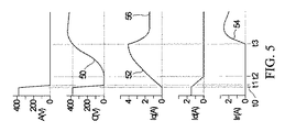
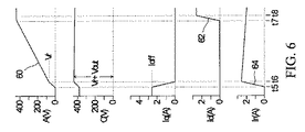
より具体的には、図4から図6の各々は、図2の接続点AおよびCのそれぞれの電圧波形AおよびCをボルト(V)単位で示すとともに、図2の矢印によって示されるように、スイッチ12の電流Iq(スイッチ12を構成するMOSFETのドレイン−ソース電流)、ブーストダイオード14の電流Idおよび抵抗22の電流Irについての電流波形Iq、IdおよびIrをアンペア(A)単位で示す。図4は、スイッチングサイクル全体の波形を示す図であり、図5および図6は、スイッチ12のターンオンおよびターンオフ時刻付近を拡大した時間軸における波形をそれぞれ示す図である。たとえば、図4の時刻t0から時刻t10までの1つのスイッチングサイクルの期間は10μsであり、図5の時
刻t0から時刻t3までの期間はおよそ80nsのオーダであり、図6の時刻t5から時刻t8までの期間はおよそ50nsのオーダである。
More specifically, each of FIGS. 4 to 6 shows respective voltage waveforms A and C at connection points A and C in FIG. 2 in volt (V) units and as indicated by arrows in FIG. The current waveforms Iq, Id and Ir for the current Iq of the switch 12 (the drain-source current of the MOSFET constituting the switch 12), the current Id of the
これらの波形は、以下の要素値および特性を有する昇圧コンバータについて説明したものであり、十分な理解が得られることを補助するために、一例としてここに与えられ、本発明はこれらの値または特性のいずれによって多少なりとも制限されない。 These waveforms are described for a boost converter having the following element values and characteristics, and are given here as an example to assist in obtaining a full understanding, and the present invention provides these values or characteristics: It is not limited in any way.
出力電圧 Vout :385V インダクタ20 :5μH
スイッチング周波数 :100kHz 抵抗22 :25Ω
ブーストインダクタ10 :800μH キャパシタンス28 :300pF
出力キャパシタ16 :50μF 出力電力 :400W
本発明の他の実施の形態においては、これらの値の全ては全く異なってもよい。ほんの一例として、キャパシタンス28は、MOSFETスイッチ12の激しい駆動を抑えることで、数nF増加させることができ、または、低出力電圧の昇圧コンバータにおいては、それはブーストダイオード14の寄生キャパシタンスまで、潜在的に減少させることもできる。
Output voltage Vout: 385 V Inductor 20: 5 μH
Switching frequency: 100 kHz Resistance 22: 25Ω
Boost inductor 10: 800 μH Capacitance 28: 300 pF
Output capacitor 16: 50 μF Output power: 400 W
In other embodiments of the invention, all of these values may be quite different. By way of example only, the
特に図4および図5を参照して、スイッチ12を構成するMOSFETをターンオンするために、制御信号Gをhighとする時刻t0の直前は、電流Idを入力Vinから出力接続点Voutまで、インダクタ10および20を介して導通するために、ダイオード14には順バイアスがかけられ、電流IqおよびIrはほぼゼロであり、接続点AおよびCはほぼ出力電圧Voutである。(接続点Aは、実際には、優勢な電流Idにおいてダイオード14の順電圧によって接続点Cよりも、より正となる。)
制御信号G(図示せず)がhighになった時刻t0から開始して、図5に示される、すぐ後の時刻t1まで、MOSFETは、接続点Aにおける電圧がほぼゼロに急速に低下するように、ターンオンする(スイッチ12が閉じられる)。ダイオード14に直列のインダクタ20により、t0〜t1の短い間隔の間、ダイオード14およびインダクタ20の電流Idはほとんど変化せず、ダイオード14には順バイアスがかけられたままであり、接続点Cにおける電圧も、時刻t1においてほぼゼロに低下する。
4 and 5 in particular, immediately before time t0 when the control signal G is high in order to turn on the MOSFET constituting the
Starting from the time t0 when the control signal G (not shown) becomes high and until the time t1 shown in FIG. 5 immediately thereafter, the MOSFET causes the voltage at the connection point A to drop rapidly to almost zero. To turn on (switch 12 is closed). Due to the
したがって、図5に示されるように、t0〜t1の間隔においては、MOSFETスイッチ12は、非常に少ない電流Iqで、すなわちほとんどゼロ電流スイッチング(Zero Current Switching:ZCS)の状態で比較的少ないスイッチング損失でターンオンされる。時刻t1において、MOSFETスイッチ12は完全にターンオンされ、出力電圧Voutがインダクタ20に発生する。それに応じて、順バイアスがかけられたダイオード14およびインダクタ20の電流Idは、時刻t1から線形的に徐々に低下し、図5に示されるように、時刻t1のやや後の時刻t2においてゼロに達する。
Therefore, as shown in FIG. 5, in the interval from t0 to t1, the
電流Idがゼロに到達する時刻t2において、ダイオード14は逆バイアスがかけられ、図5の曲線50によってよく示されるように、キャパシタンス28がインダクタ20を介して充電されるために、接続点Cの電圧がほぼゼロから共振的に上昇する。共振は、接続点Cの電圧を、時刻t3で出力電圧Voutよりオーバシュートさせ、それに続いてダイオード24に順バイアスがかけられて、電流Irが図5の曲線54でよく示されるようにほぼゼロから上昇し、インダクタ20に蓄えられたエネルギは抵抗22で消費される。
At time t2 when current Id reaches zero,
図4および図5の曲線52で示されるように、時刻t0から時刻t2までは、電流Iqは、その期間に電流Idが低下するのと逆の形で増加し、時刻t2から時刻t3までは、上述のように接続点Cの電圧が共振的に上昇するので、インダクタ20およびキャパシタンス28を経由して流れる電流により、電流Iqは上昇し続ける。時刻t3において、ダイオード24に順バイアスがかけられ始めると、電流Iqは、時刻t2におけるその値に
相当する定常状態値まで低下し、その値は時刻t0における電流Idの値である。MOSFETスイッチ12の周期の残りの期間は、時刻t5までは図4の直線56でよく示されるように、MOSFETスイッチ12の電流Iqは、閉じられたスイッチ12によって入力電圧Vinがブーストインダクタ10にかかるので、この定常状態値から値Ioffまで徐々に増加する。
As shown by the
具体的には、図4および図6を参照して、MOSFETスイッチ12をターンオフさせるために、制御信号Gがlowになる時刻t5の直前は、接続点Aは0V、接続点Cはほぼ出力電圧Voutであり、キャパシタンス28は出力電圧Voutに充電されダイオード14には逆バイアスがかけられるので、電流IdおよびIrがほぼゼロとなる。MOSFETスイッチ12がオンであり、その電流Iqはブーストインダクタ10を介して導通され、図4および図6に示されるようにIoffの値を有する。
Specifically, referring to FIGS. 4 and 6, in order to turn off
制御信号G(図示せず)がlowになる時刻t5からMOSFETが完全にターンオフされる時刻t6までの期間は、MOSFETスイッチ12がターンオフされる(スイッチ12が開放される)。このt5〜t6の期間において、MOSFETスイッチ12の電流IqはIoffの値からほぼゼロに低下する。インダクタ10および20の電流は即座には変化しないので、インダクタ10の電流はキャパシタ28、抵抗22およびダイオード24を介して出力接続点Voutへ流れ、接続点Aの電圧は急速に値Vr=R・Ioffまで上昇する。ここで、Rは抵抗22の抵抗値である。接続点Cの電圧は、Vr+Voutの値に応答して増加され、これによってダイオード24に順バイアスがかかり、直線64で示されるように、抵抗22およびダイオード24の電流Irが、時刻t6において、ほぼIoffの値まで増加する。
During a period from time t5 when the control signal G (not shown) becomes low to time t6 when the MOSFET is completely turned off, the
時刻t6から時刻t7まで、キャパシタンス28は、インダクタ10、キャパシタンス28、抵抗22および順バイアスをかけられたダイオード24を介して流れる比較的一定な電流Irによって、ほぼ線形に放電されるので、接続点Aの電圧は、図6の直線60でよく示されるように、ほぼ線形に増加する。時刻t7において、接続点Aにおける電圧は、接続点Cおよび順バイアスがかけられたダイオード14の電圧より大きい値まで増加し、それに応じて導通が開始され、図6の直線62でよく示されるように、時刻t7から、ダイオード24がインダクタ10を介して流れる全ての電流を導通する時刻t8まで、電流Idが増加する。
From time t6 to time t7,
それに続く時刻t8において、図4に示されるように、接続点AおよびCの電圧は、ほぼ出力電圧Voutまで低下し、電流Irはほぼゼロに低下する。そして、インダクタ10、ダイオード14および(電流Irがほぼゼロまで低下したときには)インダクタ20を通って流れる電流Idは、図4の直線66に示されるように、スイッチングサイクルが繰り返される時刻t10まで徐々に減少する。時刻10において、電流Idは時刻t0とほぼ同じ値に到達する。
At the subsequent time t8, as shown in FIG. 4, the voltages at the connection points A and C drop to almost the output voltage Vout, and the current Ir drops to almost zero. Then, the current Id flowing through the
抵抗22の抵抗値Rおよびキャパシタンス28大きさは、望ましくは、MOSFETスイッチ12がターンオフしている間に、接続点Aに与えられる電圧Vrが、出力電圧Voutのほんの一部となるように選択され、たとえば、図6に示されるように、385Vのオーダの出力電圧Voutに対して、60Vまたはそれより小さいオーダとなる。したがって、MOSFETスイッチ12がターンオフする際のスイッチング損失は、大きく減少される。たとえば、図2のコンバータにおけるターンオフスイッチング損失は、スナバを有しない同様のコンバータに対するスイッチング損失の15%またはそれより小さいオーダとなる。
The resistance value R and the
さらに、t0〜t2の期間が、MOSFETスイッチ12のターンオンの期間t0〜t
1よりも実質的に大きくなるのに十分となるように、インダクタ20のインダクタンスを選択することによって、MOSFETスイッチ12のターンオン時のスイッチング損失は、上述のように減少し、たとえば、スナバを有しない同様のコンバータの20%またはそれより小さくなる。さらに、図2のコンバータのダイオード14の順バイアスが、MOSFETスイッチが完全にターンオンされた後まで維持されるので、ダイオード逆回復の問題が防止される。
Further, the period from t0 to t2 is the period when the
By selecting the inductance of the
したがって、図2のコンバータにはまだいくつかの損失はあるものの、スナバを有しないコンバータの損失と比較して、大幅に減少される。抵抗24での電力消費は、たとえば、コンバータの出力電力の1%のオーダとすることができる。同時に、ダイオード逆回復問題が防止され、図2のコンバータは非常に高速の、または非常に高価なダイオードを必要しない。図2のコンバータのこれらの有利な点は、追加のスイッチおよびその駆動回路を必要とせず、上述のようなソフトスイッチング昇圧コンバータの、相対的な複雑さおよび関連するコストなしで達成される。それらはまた、図1のコンバータのようなダイオード26も必要とせず、結果としておこるそのようなダイオードを通る循環電流の発生もない。
Thus, although there is still some loss in the converter of FIG. 2, it is greatly reduced compared to the loss of the converter without the snubber. The power consumption at the
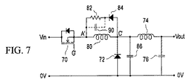
上記の説明は、昇圧コンバータに関連するが、スイッチング損失およびダイオード逆回復の同様の問題は、たとえば、降圧コンバータを含む他の電力コンバータにおいても生じ、本発明の実施の形態に従った、上述と同様の方法で対処することができる。たとえば、図7は、本発明の他の実施の形態に従った降圧コンバータを示す図である。 Although the above description relates to a boost converter, similar problems of switching losses and diode reverse recovery also occur in other power converters including, for example, a buck converter, and are described above according to embodiments of the present invention. A similar method can be used. For example, FIG. 7 shows a step-down converter according to another embodiment of the present invention.
図7を参照して、ここで示された降圧コンバータは、ゲートに供給される制御信号G’によって制御されるMOSFETスイッチ70を備え、正の入力電圧Vinのための端子と、Vinより小さい正の出力電圧Voutのための端子との間の出力インダクタ74に直列に結合される。また、降圧コンバータは、アノードが0Vラインに接続され、カソードがMOSFETスイッチ70と出力インダクタ74との間の点に結合されたダイオード72と、正の出力電圧端子および0Vライン間に結合された出力キャパシタ76とを含む。したがって、図7の降圧コンバータにおいては、MOSFETスイッチ70およびインダクタ74は、コンバータの入力および出力端子間の直列の経路に直列に結合され、ダイオード72は、コンバータのシャント経路に接続される。
Referring to FIG. 7, the step-down converter shown here includes a
図7の降圧コンバータは、MOSFETスイッチ70および出力インダクタ74の間に直列のインダクタ80と、MOSFETスイッチ70のボディダイオードと同じ導通方向に分極されたダイオード84を有するインダクタ80に並列の、直列接続された抵抗82およびダイオード84と、ダイオード72に並列のキャパシタンス86とを備えるスナバをさらに含む。インダクタ80は、典型的には、出力インダクタ74よりずっと小さいインダクタンス有する。比較的低い出力電圧では、典型的には、キャパシタンス86は、図2の昇圧コンバータのキャパシタンス28より大きく、抵抗82の抵抗値は、典型的には、図2の昇圧コンバータの抵抗22より小さくなる。
The step-down converter of FIG. 7 is connected in series in parallel with an
図7はまた、MOSETスイッチ70のソースとインダクタ80との接続点A’、およびダイオード72のカソードとインダクタ80および74との接続点C’を示しており、以下にこれらを説明する。図7の降圧コンバータは、上記で詳述した、図2の昇圧コンバータの動作と相互に関連するような方法で動作し、以下に要約する。
FIG. 7 also shows a connection point A 'between the source of the
MOSFETスイッチ70がターンオンされる直前は、接続点A’およびC’はほぼ0Vであり、MOSFET70および抵抗82を通る電流はほぼゼロであり、ダイオード72には順バイアスがかけられて、インダクタ74を介してキャパシタ76および出力に電流を導通している。制御信号G’の制御により、MOSFETスイッチ70が急速にター
ンオンされ、接続点A’の電圧が入力電圧Vinまで急激に上昇し、ダイオード72にはまだ順バイアスがかけられその電流は比較的ゆっくりとゼロまで徐々に減少し、MOSFETスイッチ70を通る電流は、反対に増加する。そして、接続点C’の電圧は、ダイオード84に順バイアスがかけられるまで、キャパシタンス86およびインダクタ80によって共振的に上昇し、MOSFETスイッチ70を通る電流が上昇する。インダクタ80のエネルギは抵抗82で消費され、MOSFTEスイッチ70を通る電流は、これに応じて、定常状態まで低下し、そこから、MOSFETスイッチがターンオフされるまでゆっくりと増加し、接続点C’の電圧は出力電圧Voutまで低下し、その電圧でキャパシタンス86が充電される。
Just before MOSFET switch 70 is turned on, nodes A ′ and C ′ are approximately 0V, the current through
制御信号G’がMOSFETスイッチ70をターンオフすると、インダクタ80を通る電流は、スイッチにかわって、ダイオード84および抵抗82を介して流れる。したがって、スイッチ電流はゼロまで急速に低下し、接続点A’の電圧は、この電流および抵抗82の抵抗値の積によって急速に低下する。そして、接続点A’およびC’の電圧は、接続点A’の電圧が負になり接続点C’の電圧がゼロをまたぎそしてダイオード72に順バイアスがかけられるまで、比較的ゆっくりと低下する。そして、電流は、ダイオード72および出力インダクタ74を介して流れ、MOSFETスイッチ70が次にターンオンされるまでゆっくりと徐々に減少し、接続点A’およびC’の電圧はほぼゼロに戻り抵抗82を通る電流はゼロに低下する。
When control signal G 'turns off
MOSFETスイッチング70は、直列接続された抵抗82およびダイオード84に並列のインダクタ80に直接的に直列接続されるので、これらの位置を交換することができることがわかるであろう。したがって、直列接続された抵抗82およびダイオード84に並列のインダクタ80を、入力電圧Vinのための端子と、MOSFETスイッチ70との間に接続することもできる。いずれの場合においても、インダクタ80は、MOSFETスイッチ70と直列であり、コンバータの入力および出力端子間の直列の経路に直列となる。
It will be appreciated that the MOSFET switching 70 is interchangeable directly in series with an
降圧コンバータの他の回路配列が図8に示され、この構成においては、図7のようにMOSFETスイッチ70に直列に接続されることに代えて、インダクタ80およびそれに並列の直列接続された抵抗82およびダイオード84は、ダイオード72およびそれに並列のキャパシタンス86に直列に、すなわちコンバータのシャント経路に接続される。したがって、図8に示されるように、インダクタ80、および同様に直列接続された抵抗82およびダイオード84は、ダイオード72のカソードと、MOSFETスイッチ70および出力インダクタ74の間の接続点との間に接続される。
Another circuit arrangement of the step-down converter is shown in FIG. 8. In this configuration, instead of being connected in series to the
あるいは、ダイオード72のカソードは、MOSFETスイッチ70および出力インダクタ74の間の接続点と接続されてもよく、インダクタ80は、ダイオード72のアノードおよび0Vラインの間に接続にされてもよく、キャパシタンス86はダイオード72と並列に、そして直列接続された抵抗82およびダイオード84はインダクタ80に並列に接続される。
Alternatively, the cathode of
図2,3,7、および8の各々の電力コンバータ、そして上述したその代替の各々においては、スナバインダクタ20または80が、コンバータスイッチ12または70と、コンバータダイオード14または72との両方を含む直列の経路となるように設けられる。インダクタ20または80は、MOSFETスイッチ12または70がターンオンされるときに、コンバータダイオード14または72を通る電流の非常に急激な変化を抑制するので、MOSFETスイッチが完全にターンオンされた後まで、ダイオードが順バイアスのままとなる。さらに、これらの電力コンバータおよび上述したその代替の各々において、直列接続された抵抗22または82、およびダイオード24または84は、スナバイン
ダクタ20または80に並列に接続され、キャパシタンス28または86は、コンバータダイオード14または72のキャパシタンスによってそれが提供されない限り、このダイオードに並列に追加される。本発明は、また、降圧または昇圧コンバータや、他の電力コンバータ、そしてモータ制御、リレー制御などのために用いられ、同様の関連ある特性を有するような他の回路における他の回路配列に適応する。
In each of the power converters of FIGS. 2, 3, 7, and 8, and each of its alternatives described above, a
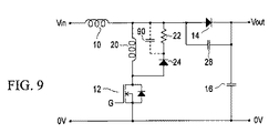
これから、たとえば、本発明の他の実施の形態が、図9に示されるような昇圧コンバータに適合できることがわかる。 From this, it can be seen that, for example, another embodiment of the present invention can be adapted to a boost converter as shown in FIG.
図9を参照して、図9においては、図2および図3の昇圧コンバータと同様の要素が用いられ、同じ参照符号が付されており、インダクタ20、およびインダクタ20に並列な直列接続された抵抗22およびダイオード24が、コンバータMOSFETスイッチ12およびブーストダイオード14を含む経路の異なった位置、この場合にはコンバータのシャント経路であり、MOSFETスイッチ12のドレインと、インダクタ10およびダイオード14の接続点との間に移される。キャパシタンス28は、ダイオード14に並列に接続される。
Referring to FIG. 9, in FIG. 9, elements similar to those of the boost converter of FIGS. 2 and 3 are used, are denoted by the same reference numerals, and are connected in series to
図9の昇圧コンバータは、コンバータのシャント経路において、抵抗22およびダイオード24をインダクタ20に並列のまま、MOSFETスイッチ12およびインダクタ20の位置を入れ替えること、および/または直列接続された抵抗22およびダイオード24の位置を入れ替えることによってさらに修正することができることがわかる。
The boost converter of FIG. 9 replaces the position of the
さらに、直列接続された抵抗22または82とダイオード24または84とが、インダクタ20または80と並列である、スナバインダクタ20または80は、昇圧コンバータの場合にはMOSFETスイッチ12と出力キャパシタ16との間、降圧コンバータの場合には0V入力端子とコンバータダイオード72との間の0Vラインの位置に代わりに移されてもよいことがわかる。
In addition, a
図10から図12は、本発明のさらなる実施の形態に従う、図2の昇圧コンバータの修正を示す図である。同様の修正は、図3および図7から図9のコンバータにも適用可能である。 FIGS. 10-12 illustrate modifications of the boost converter of FIG. 2 in accordance with a further embodiment of the present invention. Similar modifications can be applied to the converters of FIGS. 3 and 7-9.
図10においては、図2の昇圧コンバータは、抵抗22に並列な追加のキャパシタ90を設けることによって修正される。キャパシタ90の追加は、抵抗22にかかるピーク電圧および通過するピーク電流を低減できるという利点がある。この場合において、抵抗22を通過する電流は、より長い時間流れるので、抵抗22によって消費される電力の変化はない。この抵抗22に並列のキャパシタ90は、図7から図9において、これらの図の電力コンバータに付随的に設けられてもよいことを示すために、破線で示されている。
In FIG. 10, the boost converter of FIG. 2 is modified by providing an
図11では、図10の昇圧コンバータは、キャパシタ28の中にキャパシタ90のキャパシタンスを含むことによってさらに修正され、したがって、ダイオード14のアノードと、抵抗22およびダイオード24間の接続点との間に接続される。したがって、キャパシタ28は、直列のダイオード14と抵抗22とに、並列に接続される。図12では、抵抗22およびダイオード24の直列の順序が逆転されており、キャパシタ28はダイオード14のアノードと、抵抗22およびダイオード24間の接続点との間に接続される。したがって、この場合には、キャパシタ28は、直列のダイオード14とダイオード24
とに並列に接続される。
In FIG. 11, the boost converter of FIG. 10 is further modified by including the capacitance of
And connected in parallel.
キャパシタ28または90の端子が実質的に直流レベルの点に接続されたいずれの例においても、代わりに、実質的に直流レベルの他のどのような点に接続されてもよいことが
わかる。たとえば、図3の昇圧コンバータにおいて、ダイオード14のアノードと、ほぼ直流出力電圧Voutであるダイオード14のカソードとの間に接続する代わりに、キャパシタ28はダイオード14のアノードと0Vラインとの間に接続されてもよい。図3のコンバータに対して、この原理および図11または図12の修正を適用することによって、キャパシタ28は、図3に示された順序または逆の順序で直列接続された抵抗22およびダイオード24の間の接続点と、ほぼ直流出力電圧Voutあるいは0Vラインであるダイオード14のカソード、または、もし直流入力電圧の場合は電圧Vinのための端子のいずれかとの間に、代わりに接続されてもよい。
It will be appreciated that in any instance where the terminals of
以上のように、本発明の特別な実施の形態は一例の目的として上述され、数多くの修正、変形および適用が、特許請求の範囲で定義される本発明の範囲から逸脱することなく行なわれてもよいことが理解される。 Thus, the specific embodiments of the present invention have been described above by way of example, and numerous modifications, variations and applications may be made without departing from the scope of the invention as defined in the claims. It is understood that
Claims (17)
2つの入力端子(Vin,0V)と、
2つの出力端子(Vout,0V)と、
前記2つの出力端子の間に結合された出力キャパシタ(16)と、
前記入力および出力端子間の直列の経路に設けられた第1のインダクタ(10)と、
制御信号(G)によって制御されるスイッチ(12)と、
ダイオード(14)とを備え、
前記入力端子に供給される入力電圧から、前記出力端子に出力電圧を生成するために、降圧または昇圧構成となるように接続され、
前記コンバータは、
前記スイッチおよび前記第1のダイオードと直列の経路に設けられた第2のインダクタ(20)と、
直列接続された抵抗(22)および第2のダイオード(24)とをさらに備え、
前記直列接続された抵抗および第2のダイオードが、前記第2のインダクタに並列に設けられることを特徴とする、電力コンバータ。 A power converter,
Two input terminals (Vin, 0V);
Two output terminals (Vout, 0V);
An output capacitor (16) coupled between the two output terminals;
A first inductor (10) provided in a series path between the input and output terminals;
A switch (12) controlled by a control signal (G);
A diode (14),
In order to generate an output voltage from the input voltage supplied to the input terminal to the output terminal, it is connected in a step-down or boost configuration
The converter is
A second inductor (20) provided in a path in series with the switch and the first diode;
A resistor (22) and a second diode (24) connected in series;
The power converter, wherein the series-connected resistor and the second diode are provided in parallel with the second inductor.
前記第1のインダクタおよび前記スイッチは、前記2つの入力端子間に直列に結合され、
前記第1のダイオードは、前記入力および出力端子間の前記直列の経路に設けられる、請求項1に記載の電力コンバータ。 The power converter has a boost configuration;
The first inductor and the switch are coupled in series between the two input terminals;
The power converter according to claim 1, wherein the first diode is provided in the series path between the input and output terminals.
前記第1のインダクタおよび前記スイッチは、前記2つの出力端子間に直列に結合され、
前記スイッチは、前記入力および出力端子間の前記直列の経路に設けられる、請求項1に記載の電力コンバータ。 The power converter has a step-down configuration;
The first inductor and the switch are coupled in series between the two output terminals;
The power converter according to claim 1, wherein the switch is provided in the series path between the input and output terminals.
前記抵抗に並列に接続されたキャパシタ(90)とを含む、請求項1〜7のいずれか1項に記載の電力コンバータ。 A capacitor (28) connected in parallel to the first diode;
The power converter according to claim 1, comprising a capacitor (90) connected in parallel with the resistor.
前記回路配列の動作中に、電流が流れる第1のインダクタ(10)と、
制御信号(G)の制御により、開放され、または閉じられるように構成されたスイッチ(12)とを備え、
前記スイッチは、前記スイッチが閉じられたときに、前記第1のインダクタの電流を導通するように構成され、
前記回路配列は、
前記スイッチが開放されたときには、前記インダクタの電流を導通するために順バイアスがかけられ、前記スイッチが閉じられたときには、逆バイアスがかけられるように構成された第1のダイオード(14)と、
前記第1のインダクタのインダクタンスよりもずっと小さいインダクタンスを有し、前記スイッチおよび前記第1のダイオードに直列の経路に設けられる、第2のインダクタ(20)と、
抵抗(22)と前記抵抗に直列に接続された第2のダイオード(24)とをさらに備え、
前記直列接続された抵抗および第2のダイオードは、第2のインダクタに並列に接続されることを特徴とする、回路配列。 A circuit arrangement,
A first inductor (10) through which current flows during operation of the circuit arrangement;
A switch (12) configured to be opened or closed under the control of a control signal (G);
The switch is configured to conduct current of the first inductor when the switch is closed;
The circuit arrangement is:
A first diode (14) configured to be forward biased to conduct current in the inductor when the switch is opened and reverse biased when the switch is closed;
A second inductor (20) having an inductance much less than that of the first inductor and provided in a path in series with the switch and the first diode;
A resistor (22) and a second diode (24) connected in series with the resistor;
The circuit arrangement according to claim 1, wherein the resistor and the second diode connected in series are connected in parallel to a second inductor.
前記入力端子を前記スイッチに結合する前記第1のインダクタと、
前記第1のインダクタおよび前記スイッチの間の接続点を前記出力端子へ結合する前記第1のダイオードとを有し、
昇圧コンバータを形成する、請求項13または14に記載の回路配置。 Input and output terminals;
The first inductor coupling the input terminal to the switch;
The first diode coupling a connection point between the first inductor and the switch to the output terminal;
15. A circuit arrangement according to claim 13 or 14 forming a boost converter.
前記出力端子を前記第1のダイオードに結合する第1のインダクタと、
前記第1のインダクタおよび前記第1のダイオードの間の接続点を前記入力端子に結合する前記スイッチとを有し、
降圧コンバータを形成する、請求項13または14に記載の回路配置。 Input and output terminals;
A first inductor coupling the output terminal to the first diode;
The switch coupling a connection point between the first inductor and the first diode to the input terminal;
15. A circuit arrangement according to claim 13 or 14 forming a step-down converter.
Applications Claiming Priority (2)
| Application Number | Priority Date | Filing Date | Title |
|---|---|---|---|
| US11/652,613 US7579814B2 (en) | 2007-01-12 | 2007-01-12 | Power converter with snubber |
| PCT/CA2008/000054 WO2008083496A1 (en) | 2007-01-12 | 2008-01-14 | Power converter with snubber |
Publications (2)
| Publication Number | Publication Date |
|---|---|
| JP2010516223A true JP2010516223A (en) | 2010-05-13 |
| JP2010516223A5 JP2010516223A5 (en) | 2011-02-10 |
Family
ID=39608300
Family Applications (1)
| Application Number | Title | Priority Date | Filing Date |
|---|---|---|---|
| JP2009545044A Pending JP2010516223A (en) | 2007-01-12 | 2008-01-14 | Power converter with snubber |
Country Status (5)
| Country | Link |
|---|---|
| US (2) | US7579814B2 (en) |
| EP (1) | EP2102975A1 (en) |
| JP (1) | JP2010516223A (en) |
| CN (1) | CN101578756B (en) |
| WO (1) | WO2008083496A1 (en) |
Cited By (4)
| Publication number | Priority date | Publication date | Assignee | Title |
|---|---|---|---|---|
| JP2013207894A (en) * | 2012-03-28 | 2013-10-07 | Murata Mfg Co Ltd | Switching power supply device |
| WO2015079538A1 (en) * | 2013-11-28 | 2015-06-04 | 株式会社安川電機 | Dc-dc converter |
| JP2016019378A (en) * | 2014-07-09 | 2016-02-01 | 株式会社デンソー | Switching power supply circuit |
| JP2021035288A (en) * | 2019-08-29 | 2021-03-01 | 日本電産株式会社 | Buck-boost chopper circuit and dc power supply device |
Families Citing this family (48)
| Publication number | Priority date | Publication date | Assignee | Title |
|---|---|---|---|---|
| EP2211448A4 (en) * | 2007-11-15 | 2013-09-11 | Fujitsu Ltd | Switcing power supply, control circuit controlling switching power supply and control method of switching power supply |
| US7915872B2 (en) * | 2008-05-14 | 2011-03-29 | Astec International Limited | Switching power converters with diode reverse current suppression |
| US8659273B2 (en) * | 2008-10-27 | 2014-02-25 | Dell Products L.P. | Soft-switching voltage regulation in a step-down circuit |
| GB2466871A (en) * | 2009-01-07 | 2010-07-14 | Champion Aerospace Inc | DC aircraft power supply having voltage modulation attenuator |
| TW201032448A (en) * | 2009-02-23 | 2010-09-01 | Delta Electronics Inc | Power conversion circuit capable of distributing input current |
| US9166471B1 (en) | 2009-03-13 | 2015-10-20 | Rf Micro Devices, Inc. | 3D frequency dithering for DC-to-DC converters used in multi-mode cellular transmitters |
| EP2230754B1 (en) * | 2009-03-18 | 2015-04-29 | STMicroelectronics (Tours) SAS | Switching mode power supply |
| US20120049834A1 (en) * | 2009-05-07 | 2012-03-01 | The Curators Of The University Of Missouri | Circuit and method to suppress the parasitic resonance from a dc/dc converter |
| US8548398B2 (en) | 2010-02-01 | 2013-10-01 | Rf Micro Devices, Inc. | Envelope power supply calibration of a multi-mode radio frequency power amplifier |
| US9184701B2 (en) * | 2010-04-20 | 2015-11-10 | Rf Micro Devices, Inc. | Snubber for a direct current (DC)-DC converter |
| US9900204B2 (en) | 2010-04-20 | 2018-02-20 | Qorvo Us, Inc. | Multiple functional equivalence digital communications interface |
| US9362825B2 (en) | 2010-04-20 | 2016-06-07 | Rf Micro Devices, Inc. | Look-up table based configuration of a DC-DC converter |
| US9553550B2 (en) | 2010-04-20 | 2017-01-24 | Qorvo Us, Inc. | Multiband RF switch ground isolation |
| US9077405B2 (en) | 2010-04-20 | 2015-07-07 | Rf Micro Devices, Inc. | High efficiency path based power amplifier circuitry |
| US9008597B2 (en) | 2010-04-20 | 2015-04-14 | Rf Micro Devices, Inc. | Direct current (DC)-DC converter having a multi-stage output filter |
| US9577590B2 (en) | 2010-04-20 | 2017-02-21 | Qorvo Us, Inc. | Dual inductive element charge pump buck and buck power supplies |
| US9214865B2 (en) | 2010-04-20 | 2015-12-15 | Rf Micro Devices, Inc. | Voltage compatible charge pump buck and buck power supplies |
| US9214900B2 (en) | 2010-04-20 | 2015-12-15 | Rf Micro Devices, Inc. | Interference reduction between RF communications bands |
| JP5429032B2 (en) * | 2010-05-07 | 2014-02-26 | 三菱電機株式会社 | Power conversion circuit |
| JP2011239545A (en) * | 2010-05-10 | 2011-11-24 | Sanken Electric Co Ltd | Dc-dc converter |
| JP5496038B2 (en) | 2010-09-22 | 2014-05-21 | 三菱電機株式会社 | DC-DC converter |
| KR20130114670A (en) * | 2010-10-05 | 2013-10-17 | 에이비비 테크놀로지 아게 | Rectifier circuit |
| JP2012120362A (en) * | 2010-12-02 | 2012-06-21 | Sanken Electric Co Ltd | Dc-dc converter |
| TWI439023B (en) * | 2011-07-13 | 2014-05-21 | Wistron Corp | Low noise step-down converter and low noise voltage supply assembly |
| CN102931845A (en) * | 2011-08-12 | 2013-02-13 | 旭丽电子(广州)有限公司 | Voltage boosting conversion device and voltage boosting conversion circuit |
| US20130063099A1 (en) * | 2011-09-11 | 2013-03-14 | Yen-Wei Hsu | High electrical field driver |
| JP2013069859A (en) * | 2011-09-22 | 2013-04-18 | Toshiba Corp | Semiconductor device |
| US9065505B2 (en) | 2012-01-31 | 2015-06-23 | Rf Micro Devices, Inc. | Optimal switching frequency for envelope tracking power supply |
| EP2648483B1 (en) | 2012-04-06 | 2019-08-07 | Dialog Semiconductor GmbH | Method of preventing spurious ringing during discontinuous conduction mode in inductive boost converters for white LED drivers |
| CN102830740B (en) * | 2012-08-23 | 2014-04-30 | 矽力杰半导体技术(杭州)有限公司 | High-efficiency bias voltage generating circuit |
| US20140119058A1 (en) * | 2012-10-30 | 2014-05-01 | Chicony Power Technology Co., Ltd. | Power voltage conversion system for controller integrated circuit |
| CN103856054A (en) * | 2012-12-06 | 2014-06-11 | 东林科技股份有限公司 | Isolated power conversion device and power conversion method thereof |
| KR101998078B1 (en) | 2012-12-10 | 2019-07-09 | 삼성전자 주식회사 | Hybrid charge pump and method for operating the same, power management IC comprising the pump, and display device comprsing the PMIC |
| DE102013104529A1 (en) * | 2013-05-03 | 2014-11-06 | Sma Solar Technology Ag | Step-up or step-down converter with discharge capacitor |
| CN104660069A (en) * | 2013-11-18 | 2015-05-27 | 东林科技股份有限公司 | Power conversion device and conversion method thereof |
| KR102317140B1 (en) * | 2014-02-19 | 2021-10-22 | 엘지전자 주식회사 | Power converting apparatus, and photovoltaic module |
| KR20150115561A (en) * | 2014-04-04 | 2015-10-14 | 삼성에스디아이 주식회사 | Apparatus for power conditioning system of solar photovoltaic |
| TWI524638B (en) * | 2014-05-23 | 2016-03-01 | 華碩電腦股份有限公司 | Boost converter and power supplying method |
| US9699849B2 (en) * | 2015-06-26 | 2017-07-04 | EPtronics, Inc. | LED driver which can be used with either trailing edge or leading edge dimmers |
| CN105634275A (en) * | 2016-03-23 | 2016-06-01 | 西安工业大学 | Boost converter of switch inductor |
| DE112019001683T5 (en) * | 2018-06-15 | 2021-03-11 | Murata Manufacturing Co., Ltd. | RC SNUBBER LINK |
| JP7018030B2 (en) * | 2019-01-24 | 2022-02-09 | 株式会社京三製作所 | DC pulse power supply |
| JP6858805B2 (en) * | 2019-04-11 | 2021-04-14 | 株式会社京三製作所 | Frequency control method for DC pulse power supply and DC pulse power supply |
| TWI696349B (en) * | 2019-05-31 | 2020-06-11 | 遠東科技大學 | High voltage gain step-up converter |
| CN110350816B (en) * | 2019-07-16 | 2020-10-09 | 福州大学 | Single-stage single-phase current type inverter with energy storage inductor connected with active buffer circuit in parallel |
| CN113258755B (en) * | 2020-02-13 | 2022-07-26 | 宏碁股份有限公司 | Boost converter |
| CA3174967A1 (en) * | 2020-04-21 | 2021-10-28 | Alex S. Creviston | Adaptable precharge |
| CN114204802B (en) * | 2021-11-17 | 2023-05-16 | 深圳技术大学 | Charging circuit |
Citations (3)
| Publication number | Priority date | Publication date | Assignee | Title |
|---|---|---|---|---|
| JPH01138966A (en) * | 1987-11-25 | 1989-05-31 | Matsushita Electric Works Ltd | Dc-dc converter |
| JPH09117130A (en) * | 1995-08-31 | 1997-05-02 | Samsung Electro Mech Co Ltd | Boost type converter circuit |
| JPH10248243A (en) * | 1997-02-28 | 1998-09-14 | Fuji Electric Co Ltd | Power conversion circuit |
Family Cites Families (22)
| Publication number | Priority date | Publication date | Assignee | Title |
|---|---|---|---|---|
| JPS59172945A (en) * | 1983-03-22 | 1984-09-29 | Victor Co Of Japan Ltd | Dc high voltage generator |
| JP2600920B2 (en) * | 1989-08-30 | 1997-04-16 | 富士電機株式会社 | Horizontal deflection circuit |
| US5446366A (en) | 1994-02-08 | 1995-08-29 | Computer Products, Inc. | Boost converter power supply with reduced losses, control circuit and method therefor |
| US5550458A (en) | 1994-05-31 | 1996-08-27 | Lucent Technologies Inc. | Low-loss snubber for a power factor corrected boost converter |
| KR970008828B1 (en) | 1994-07-21 | 1997-05-29 | Korea Telecommunication | Energy regenerating snoover using booster converter |
| US5642267A (en) * | 1996-01-16 | 1997-06-24 | California Institute Of Technology | Single-stage, unity power factor switching converter with voltage bidirectional switch and fast output regulation |
| US5736842A (en) | 1996-07-11 | 1998-04-07 | Delta Electronics, Inc. | Technique for reducing rectifier reverse-recovery-related losses in high-voltage high power converters |
| SE511059C2 (en) * | 1997-01-24 | 1999-07-26 | Ericsson Telefon Ab L M | Method and device for power conversion. |
| US5909107A (en) * | 1997-02-10 | 1999-06-01 | Tdk Corporation | Step up switching power unit and filter circuit |
| US5943200A (en) | 1998-01-06 | 1999-08-24 | Lucent Technologies Inc. | Peak voltage clamping circuit for high frequency boost converter and method of operation thereof |
| US5969515A (en) * | 1998-02-27 | 1999-10-19 | Motorola, Inc. | Apparatus and method for digital control of a power converter current |
| US6345238B1 (en) * | 1998-12-21 | 2002-02-05 | Airpax Corporation, Llc | Linear temperature sensor |
| US6051961A (en) | 1999-02-11 | 2000-04-18 | Delta Electronics, Inc. | Soft-switching cell for reducing switching losses in pulse-width-modulated converters |
| US6259235B1 (en) * | 1999-08-26 | 2001-07-10 | Tyco Electronics Logistics Ag | Active clamp for power converter and method of operation thereof |
| US6194880B1 (en) * | 1999-10-22 | 2001-02-27 | Lucent Technologies Inc. | Boost converter, method of converting power and power supply employing the same |
| FR2821996B1 (en) * | 2001-03-09 | 2003-06-13 | St Microelectronics Sa | CIRCUIT FOR SWITCHING A CUT-OUT CONVERTER |
| JP2003189602A (en) * | 2001-12-17 | 2003-07-04 | Murata Mfg Co Ltd | Dc-dc converter and electric equipment using the same |
| CN1170359C (en) | 2002-05-27 | 2004-10-06 | 艾默生网络能源有限公司 | Low-loss step-up method and device |
| JP4534223B2 (en) * | 2004-04-30 | 2010-09-01 | ミネベア株式会社 | DC-DC converter |
| DE102004022571A1 (en) * | 2004-05-07 | 2005-12-08 | Patent-Treuhand-Gesellschaft für elektrische Glühlampen mbH | Electronic ballast for a lamp |
| DE102004050060B4 (en) * | 2004-10-13 | 2018-02-08 | Osram Gmbh | Buck converter circuit |
| US7233507B2 (en) * | 2005-05-18 | 2007-06-19 | Optimum Power Conversion, Inc. | Non dissipative snubber circuit with saturable reactor |
-
2007
- 2007-01-12 US US11/652,613 patent/US7579814B2/en not_active Expired - Fee Related
-
2008
- 2008-01-14 WO PCT/CA2008/000054 patent/WO2008083496A1/en active Application Filing
- 2008-01-14 JP JP2009545044A patent/JP2010516223A/en active Pending
- 2008-01-14 EP EP08706202A patent/EP2102975A1/en not_active Withdrawn
- 2008-01-14 CN CN2008800021814A patent/CN101578756B/en not_active Expired - Fee Related
-
2009
- 2009-06-30 US US12/495,010 patent/US7915876B2/en not_active Expired - Fee Related
Patent Citations (3)
| Publication number | Priority date | Publication date | Assignee | Title |
|---|---|---|---|---|
| JPH01138966A (en) * | 1987-11-25 | 1989-05-31 | Matsushita Electric Works Ltd | Dc-dc converter |
| JPH09117130A (en) * | 1995-08-31 | 1997-05-02 | Samsung Electro Mech Co Ltd | Boost type converter circuit |
| JPH10248243A (en) * | 1997-02-28 | 1998-09-14 | Fuji Electric Co Ltd | Power conversion circuit |
Cited By (6)
| Publication number | Priority date | Publication date | Assignee | Title |
|---|---|---|---|---|
| JP2013207894A (en) * | 2012-03-28 | 2013-10-07 | Murata Mfg Co Ltd | Switching power supply device |
| WO2015079538A1 (en) * | 2013-11-28 | 2015-06-04 | 株式会社安川電機 | Dc-dc converter |
| US9876423B2 (en) | 2013-11-28 | 2018-01-23 | Kabushiki Kaisha Yaskawa Denki | DC-to-DC converter |
| JP2016019378A (en) * | 2014-07-09 | 2016-02-01 | 株式会社デンソー | Switching power supply circuit |
| JP2021035288A (en) * | 2019-08-29 | 2021-03-01 | 日本電産株式会社 | Buck-boost chopper circuit and dc power supply device |
| JP7347010B2 (en) | 2019-08-29 | 2023-09-20 | ニデック株式会社 | Buck-boost chopper circuit and DC power supply |
Also Published As
| Publication number | Publication date |
|---|---|
| CN101578756A (en) | 2009-11-11 |
| US20080169792A1 (en) | 2008-07-17 |
| CN101578756B (en) | 2012-11-28 |
| US20090267576A1 (en) | 2009-10-29 |
| US7579814B2 (en) | 2009-08-25 |
| US7915876B2 (en) | 2011-03-29 |
| EP2102975A1 (en) | 2009-09-23 |
| WO2008083496A1 (en) | 2008-07-17 |
Similar Documents
| Publication | Publication Date | Title |
|---|---|---|
| JP2010516223A (en) | Power converter with snubber | |
| US10381915B1 (en) | Variable delay for soft switching in power conversion circuit | |
| US7385833B2 (en) | Snubber circuit for a power converter | |
| JP6682652B2 (en) | Half-bridge resonance converter, circuit using the half-bridge resonance converter, and corresponding control method | |
| US7486055B2 (en) | DC-DC converter having a diode module with a first series circuit and a second series with a flywheel diode | |
| US7023186B2 (en) | Two stage boost converter topology | |
| US7764515B2 (en) | Two terminals quasi resonant tank circuit | |
| US7321224B2 (en) | DC-DC converter with clamping capacitor and output winding for reduced output voltage ripple | |
| US7304463B2 (en) | DC-DC converter | |
| US20100141222A1 (en) | Load transient sensing circuit for a power converter | |
| CN107294385B (en) | Method and apparatus for adaptive timing of zero voltage conversion power converters | |
| US11018592B2 (en) | Flyback converter controller, flyback converter and methods of operation | |
| US20180323713A1 (en) | Soft-switching for high-frequency power conversion | |
| JP3528920B2 (en) | Switching power supply | |
| KR101256032B1 (en) | Solid state switching circuit | |
| JP3582643B2 (en) | Step-up DC-DC converter | |
| KR20150047648A (en) | ZVZCS Switching Converter Using Auto-Transformer | |
| TW201939868A (en) | Coupled-inductor cascaded buck convertor with fast transient response | |
| JP2015228760A (en) | Switching power supply | |
| JP7329972B2 (en) | Converter and converter control method | |
| JP2001309646A (en) | Switching power unit | |
| CN115694190A (en) | Power conversion circuit | |
| Ulrich | ZVS clamp-switch quasi Z-source dc/dc boost converters | |
| JPH10210747A (en) | Switching power source and its control method | |
| Park et al. | Coupled-inductor boost converter with simple resonant technique |
Legal Events
| Date | Code | Title | Description |
|---|---|---|---|
| A521 | Written amendment |
Free format text: JAPANESE INTERMEDIATE CODE: A523 Effective date: 20101214 |
|
| A621 | Written request for application examination |
Free format text: JAPANESE INTERMEDIATE CODE: A621 Effective date: 20101214 |
|
| A131 | Notification of reasons for refusal |
Free format text: JAPANESE INTERMEDIATE CODE: A131 Effective date: 20120821 |
|
| A02 | Decision of refusal |
Free format text: JAPANESE INTERMEDIATE CODE: A02 Effective date: 20130205 |