JP2009095183A - Switching power-supply device - Google Patents
Switching power-supply device Download PDFInfo
- Publication number
- JP2009095183A JP2009095183A JP2007265241A JP2007265241A JP2009095183A JP 2009095183 A JP2009095183 A JP 2009095183A JP 2007265241 A JP2007265241 A JP 2007265241A JP 2007265241 A JP2007265241 A JP 2007265241A JP 2009095183 A JP2009095183 A JP 2009095183A
- Authority
- JP
- Japan
- Prior art keywords
- choke coil
- common mode
- circuit
- mode choke
- switching power
- Prior art date
- Legal status (The legal status is an assumption and is not a legal conclusion. Google has not performed a legal analysis and makes no representation as to the accuracy of the status listed.)
- Pending
Links
Images


Classifications
-
- Y—GENERAL TAGGING OF NEW TECHNOLOGICAL DEVELOPMENTS; GENERAL TAGGING OF CROSS-SECTIONAL TECHNOLOGIES SPANNING OVER SEVERAL SECTIONS OF THE IPC; TECHNICAL SUBJECTS COVERED BY FORMER USPC CROSS-REFERENCE ART COLLECTIONS [XRACs] AND DIGESTS
- Y02—TECHNOLOGIES OR APPLICATIONS FOR MITIGATION OR ADAPTATION AGAINST CLIMATE CHANGE
- Y02P—CLIMATE CHANGE MITIGATION TECHNOLOGIES IN THE PRODUCTION OR PROCESSING OF GOODS
- Y02P80/00—Climate change mitigation technologies for sector-wide applications
- Y02P80/10—Efficient use of energy, e.g. using compressed air or pressurized fluid as energy carrier
Landscapes
- Dc-Dc Converters (AREA)
Abstract
Description
本発明は、商用交流電源を入力とするスイッチング電源装置に関するものであり、特にスイッチング素子のスイッチングによる放射雑音や電源線路への導電性雑音を抑制したスイッチング電源装置に関する。 The present invention relates to a switching power supply apparatus that uses a commercial AC power supply as an input, and more particularly to a switching power supply apparatus that suppresses radiation noise due to switching of a switching element and conductive noise to a power supply line.
スイッチング電源においては、スイッチング素子の高速度で大電流のスイッチングにより、放射雑音や電源線への導電性雑音が発生して、他の電子機器や通信機器への障害となるので、なるべく、それら雑音は低いレベルに抑制されることが望ましい。 In switching power supplies, switching currents at high speeds and high currents cause radiation noise and conductive noise to power lines, which may interfere with other electronic equipment and communication equipment. Is preferably suppressed to a low level.
スイッチング電源装置における雑音抑制についての先行する発明としては、例えば、特開平5−191976号公報に開示されている発明がある。その発明は、力率改善回路より発生するノーマルモードノイズの低減を図ることを目的とし、その構成は、チョークコイルの二つのコイル部を半数ずつの巻数に2分割し、互いに逆極性となるように同一のコアに巻回して整流回路の出力ライン両端にそれぞれ挿入接続する。整流回路の電圧供給側ラインと接地端子との間及び、整流回路のマイナス側ラインと接地端子との間のコモンモードノイズとは互いに逆位相となって現われ、整流回路の電圧供給側ラインとマイナス側ラインとの間に生じるノーマルモードノイズは打消し合うとしている。 As a prior invention regarding noise suppression in a switching power supply device, for example, there is an invention disclosed in Japanese Patent Laid-Open No. Hei 5-191976. An object of the present invention is to reduce normal mode noise generated from the power factor correction circuit, and the configuration is such that the two coil portions of the choke coil are divided into half the number of turns so that they have opposite polarities. Are wound around the same core and inserted and connected to both ends of the output line of the rectifier circuit. The common mode noise between the voltage supply side line of the rectifier circuit and the ground terminal and between the negative side line of the rectifier circuit and the ground terminal appears in opposite phases to each other. Normal mode noise generated between the side lines cancels each other.
また、特開平6−311749号公報に開示される発明は、整流平滑回路とその交流入力端子との間に接続されたノイズフィルタとを備えたものにおいて、特性が互いにほぼ等しい一対のコモンモ−ドチョ−クコイルの従属接続体をノイズフィルタとして備えている。 Further, the invention disclosed in Japanese Patent Application Laid-Open No. 6-311749 includes a rectifying / smoothing circuit and a noise filter connected between its AC input terminals, and a pair of common mode chords having substantially the same characteristics. -A coiled slave connection is provided as a noise filter.
また、特開2001−196949号公報に開示される発明は、スイッチング電源の入力端子側に接続された第1のコモンモードフィルタと、スイッチング電源の出力端子と受信部の入力端子との間に接続された第2のコモンモードフィルタと、第1のコモンモードフィルタの入力端子と受信部の入力端子とを高周波数的に接続する高周波接続部とを備えて、第1、第2のコモンモードフィルタが、受信部の受信周波数帯域と同じ周波数成分の雑音を抑制する減衰特性を夫々に有している。 The invention disclosed in Japanese Patent Laid-Open No. 2001-196949 is connected between the first common mode filter connected to the input terminal side of the switching power supply and the output terminal of the switching power supply and the input terminal of the receiving unit. A first common mode filter, and a second common mode filter, and a high frequency connection section that connects the input terminal of the first common mode filter and the input terminal of the receiving section at a high frequency. However, each has an attenuation characteristic that suppresses noise having the same frequency component as the reception frequency band of the reception unit.
また、特開2002−354798号公報に開示される発明は、スイッチング電源装置において、主制御回路に関連して、スイッチング周波数をメモリに格納された値の第1のスイッチング周波数から第2のスイッチング周波数までの範囲で規定の周期で連続的に変化させるスイッチング周波数可変回路を設けている。
以上の先行する発明の構成は、構成部品数が多いもの、あるいは定数選定の条件がクリティカルなものである。本発明は、スイッチング電源装置において、比較的少ない構成部品数の簡素な回路構成で、定数選定の条件が緩やかで、安定して確実に雑音を減少させることを目的とする。 In the configuration of the preceding invention described above, the number of components is large, or the condition for selecting constants is critical. It is an object of the present invention to reduce noise stably and surely in a switching power supply apparatus with a simple circuit configuration having a relatively small number of components, with a constant constant selection condition.
この課題を解決するため、本発明は、以下の第1の手段を提案する。すなわち、
交流電源に接続される一対の交流入力端子と、
該交流入力端子に順次接続された第1のコモンモードチョークコイルと、
整流回路と、第2のコモンモードチョークコイルと、力率改善回路と、コンバータと、変圧器と、第2の整流回路とからなり、第2の整流回路に接続された出力端子から所定の電圧値の直流出力電圧を発生するスイッチング電源装置において、
前記第1のコモンモードチョークコイルの出力側に、直列接続された第1の直列コンデンサ列と、
前記第2のコモンモードチョークコイルの入力側に、直列接続された第2の直列コンデンサ列とを備え、
第1の直列コンデンサ列の相互接続点と第2の直列コンデンサ列の相互接続点とを共にフレームグランド端子に接続するとともに、
前記第2のコモンモードチョークコイルと前記力率改善回路との間に接続された、チョークコイルとコンデンサ二つとからなるπ形フィルタ回路を備えることを特徴とする、スイッチング電源装置を提案する。
なお、π形フィルタ回路は、一つあるいは従属接続して複数とすることができる。効果とコストなどを勘案してその数は選定できる。
In order to solve this problem, the present invention proposes the following first means. That is,
A pair of AC input terminals connected to an AC power source;
A first common mode choke coil sequentially connected to the AC input terminal;
A rectifier circuit, a second common mode choke coil, a power factor correction circuit, a converter, a transformer, and a second rectifier circuit, and a predetermined voltage from an output terminal connected to the second rectifier circuit In a switching power supply that generates a DC output voltage of
A first series capacitor string connected in series to the output side of the first common mode choke coil;
A second series capacitor array connected in series on the input side of the second common mode choke coil;
Connecting both the interconnection point of the first series capacitor row and the interconnection point of the second series capacitor row to the frame ground terminal;
The present invention proposes a switching power supply device comprising a π-type filter circuit including a choke coil and two capacitors connected between the second common mode choke coil and the power factor correction circuit.
Note that one or a plurality of π-type filter circuits can be connected in cascade. The number can be selected in consideration of effects and costs.
また、第2の手段として、
交流電源に接続される一対の交流入力端子と、
該交流入力端子に順次接続された第1のコモンモードチョークコイルと、
整流回路と、第2のコモンモードチョークコイルと、力率改善回路と、コンバータと、変圧器と、第2の整流回路とからなり、第2の整流回路に接続された出力端子から所定の電圧値の直流出力電圧を発生するスイッチング電源装置において、
前記第1のコモンモードチョークコイルの出力側に、直列接続された第1の直列コンデンサ列と、
前記第2のコモンモードチョークコイルの入力側に、直列接続された第2の直列コンデンサ列とを備え、
第1の直列コンデンサ列の相互接続点と第2の直列コンデンサ列の相互接続点とを共にチョークコイルを介してフレームグランド端子に接続するとともに、
前記第2のコモンモードチョークコイルと前記力率改善回路との間に接続された、チョークコイルとコンデンサ二つとからなるπ形フィルタ回路を備えることを特徴とする、スイッチング電源装置を提案する。
なお、π形フィルタ回路は、一つあるいは従属接続して複数とすることができる。効果とコストなどを勘案してその数は選定できる。
As a second means,
A pair of AC input terminals connected to an AC power source;
A first common mode choke coil sequentially connected to the AC input terminal;
A rectifier circuit, a second common mode choke coil, a power factor correction circuit, a converter, a transformer, and a second rectifier circuit, and a predetermined voltage from an output terminal connected to the second rectifier circuit In a switching power supply that generates a DC output voltage of
A first series capacitor string connected in series to the output side of the first common mode choke coil;
A second series capacitor array connected in series on the input side of the second common mode choke coil;
The interconnection point of the first series capacitor string and the interconnection point of the second series capacitor string are both connected to the frame ground terminal via the choke coil, and
The present invention proposes a switching power supply device comprising a π-type filter circuit including a choke coil and two capacitors connected between the second common mode choke coil and the power factor correction circuit.
Note that one or a plurality of π-type filter circuits can be connected in cascade. The number can be selected in consideration of effects and costs.
また、第3の手段として、
前記の第1の手段又は第2の手段において
前記π形フィルタ回路の二つのコンデンサの相互接続点が、前記力率改善回路のコモン線と前記コンバータのコモン線とに接続されることを提案する。
As a third means,
In the first means or the second means, it is proposed that an interconnection point of two capacitors of the π-type filter circuit is connected to a common line of the power factor correction circuit and a common line of the converter .
第1の手段において、二つのコモンモードチョークコイルによるコモンモードのフィルタ作用と、π形フィルタ回路によるノーマルモードノイズに対するフィルタ作用との相乗作用により、雑音が大きく減少する。
第2の手段については、第1の手段に加えて、第1の直列コンデンサ列の相互接続点と第2の直列コンデンサ列の相互接続点とを直接フレームグランド端子に接続する構成と、第1の直列コンデンサ列の相互接続点と第2の直列コンデンサ列の相互接続点とをチョークコイルを介してフレームグランド端子に接続する構成は、個別の回路と運転状況に応じて、より効果的に雑音を減少させることができる。
第3の手段については、第1又は第2の手段に加えて、π形フィルタ回路の二つのコンデンサの相互接続点が、力率改善回路のコモン線とコンバータのコモン線とに接続されることは、個別の回路と運転状況に応じて、より効果的い雑音を減少させることができる。
In the first means, the noise is greatly reduced by the synergistic action of the common mode filter action by the two common mode choke coils and the filter action for the normal mode noise by the π-type filter circuit.
As for the second means, in addition to the first means, a configuration in which the interconnection point of the first series capacitor row and the interconnection point of the second series capacitor row are directly connected to the frame ground terminal, The configuration in which the interconnection point of the series capacitor string and the interconnection point of the second series capacitor string are connected to the frame ground terminal via the choke coil is more effective in noise depending on the individual circuit and operating conditions. Can be reduced.
As for the third means, in addition to the first or second means, the interconnection point of the two capacitors of the π-type filter circuit is connected to the common line of the power factor correction circuit and the common line of the converter. Can reduce noise more effectively depending on the individual circuit and operating conditions.
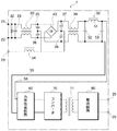
図1は、本発明に係るスイッチング電源装置の一実施例の概略図であり、以下、図1に基づき、その構成と動作を説明する。 FIG. 1 is a schematic diagram of an embodiment of a switching power supply device according to the present invention. Hereinafter, the configuration and operation will be described with reference to FIG.
スイッチング電源装置1は、入力端子21、22、コモンモードチョークコイル30、整流回路40、第2のコモンモードチョークコイル39、π形フィルタ50、昇圧チョッパ回路を含む力率改善回路60、コンバータ70、変圧器71、整流回路80、出力端子25、26から構成される。
スイッチング電源装置1の入力端子21、22は、外部の商用交流電源に接続され、これら入力端子21、22間の交流電圧は、コモンモードチョークコイル30を経て、整流回路40で整流された後、第2のコモンモードチョークコイル39とπ形フィルタ50を経て、これをコモン線路55と整流電圧線路56を介して昇圧チョッパ回路を含む力率改善回路60によって直流電圧になる。この直流電圧は、電力スイッチング素子とその制御回路とを含むコンバータ70と、変圧器71と、整流回路80とによって、目的の電圧の値の直流電圧となって、出力端子25、26間から出力される。
The switching power supply 1 includes
The
コモンモードチョークコイル30の入力側の一対の端子には、抵抗器32とコンデンサ33とが接続される。また、コモンモードチョークコイル30の出力側の一対の端子には、ほぼ等しい静電容量のコンデンサ35、36が直列接続された状態で接続される。コモンモードチョークコイル39の入力側の一対の端子にも同様に、ほぼ等しい静電容量のコンデンサ37、38が直列接続された状態で接続される。これらコンデンサ35、36の相互接続点とコンデンサ37、38の相互接続点とは、共にチョークコイル34を介して、接地用端子23に接続される。π形フィルタ50は、チョークコイル51とコンデンサ52、53とによって構成される。このπ形フィルタ50において、コンデンサ52、53の相互接続点に連なる線路55を、コモン線路として、以降の回路である力率改善回路60とコンバータ70との各コモン線路に接続される。
A
このように構成されたスイッチング電源装置1において、昇圧チョッパ回路を含む力率改善回路60は、入力電圧が交流100Vの場合と交流200Vとの場合とを何らの切替なしで定常状態で動作するように構成されている。すなわち、力率改善回路60の中の昇圧チョッパ回路の導通期間の可変幅や繰り返し周期などの動作条件によって、常に定常状態で動作するように構成されている。この力率改善回路60の中の昇圧チョッパ回路のスイッチングによる雑音の発生と、コンバータ70の中のスイッチング素子による雑音の発生とは、別々の周波数であり、また、スイッチング電源装置1の入力条件、負荷条件などの運転状況によって、雑音の発生に係るスペクトラムは、さまざまに変化する。
In the switching power supply device 1 configured as described above, the power
図2〜5に、スイッチング電源装置の実際の運転状況における伝導雑音の測定結果について、本発明を適用した場合と適用しない場合の比較を示すものであり、それら測定条件の共通事項として、測定機器は、BBS300−24、測定バンドは4バンド、検波モードはピーク、ラインモードはVAである。
図2には、本発明を適用したスイッチング電源装置1の実際の運転状態における伝導雑音の測定結果の一例を示す。入力が、交流100Vのときの測定結果であり、150kHz〜30MHzの範囲の周波数において、30dBμVないし60dBμVにある。一方、EN55022、CLASS A規格の限界線が70dBμVないし80dBμVの線にある。したがって、この限界線よりも10dB〜30dBの余裕がある。
FIGS. 2 to 5 show a comparison between the case where the present invention is applied and the case where the present invention is not applied to the measurement result of the conduction noise in the actual operation state of the switching power supply apparatus. Are BBS300-24, the measurement band is 4 bands, the detection mode is peak, and the line mode is VA.
In FIG. 2, an example of the measurement result of the conduction noise in the actual driving | running state of the switching power supply device 1 to which this invention is applied is shown. It is a measurement result when the input is 100 V AC, and is 30 dBμV to 60 dBμV in a frequency range of 150 kHz to 30 MHz. On the other hand, the limit line of EN55022, CLASS A standard is in the line of 70 dBμV to 80 dBμV. Therefore, there is a margin of 10 dB to 30 dB beyond this limit line.
この図2に示す測定条件に対して、π形フィルタ50を用いない条件、すなわち、π形フィルタ50の中のチョークコイル51を短絡した状態での測定結果を図3に示す。この測定結果では、周波数の全範囲において、30dBμVないし65dBμVであり、限界線に対して余裕がほとんどなく、運転状況の変化によっては、規格を逸脱するおそれがある。
FIG. 3 shows the measurement results obtained when the π-
本発明に係る実施例のスイッチング電源1の実際の運転状態における伝導雑音の測定結果の一例を図4に示す。入力が、交流200Vのときの測定結果であり、150kHz〜30MHzの範囲の周波数において、30dBμVないし60dBμVにある。一方、EN55022、CLASS A規格の限界線が70dBμVないし80dBμVの線にある。したがって、この限界線よりも10dB〜30dBの余裕がある。 An example of the measurement result of the conduction noise in the actual operation state of the switching power supply 1 of the embodiment according to the present invention is shown in FIG. It is a measurement result when the input is AC 200 V, and is 30 dBμV to 60 dBμV in a frequency range of 150 kHz to 30 MHz. On the other hand, the limit line of EN55022, CLASS A standard is in the line of 70 dBμV to 80 dBμV. Therefore, there is a margin of 10 dB to 30 dB beyond this limit line.
この図4に示す測定条件に対して、π形フィルタ50を用いない条件、すなわち、π形フィルタ50の中のチョークコイル51を短絡した状態での測定結果を図5に示す。この測定結果では、周波数の全範囲において、30dBμVないし75dBμVであり、限界線に対して余裕がほとんどなく、運転状況の変化によっては、規格を逸脱するおそれがある。
FIG. 5 shows a measurement result in a condition where the π-
1 スイッチング電源装置
21、22 入力端子
23 接地用端子
25、26 出力端子
30 コモンモードチョークコイル
32 抵抗器
33 コンデンサ
34 チョークコイル
35、36、37、38 コンデンサ
39 コモンモードチョークコイル
40 整流回路
50 π形フィルタ
51 チョークコイル
52、53 コンデンサ
55 コモン線路
56 整流電圧線路
60 力率改善回路
70 コンバータ
71 変圧器
80 整流回路
DESCRIPTION OF SYMBOLS 1 Switching
Claims (3)
該交流入力端子に順次接続された第1のコモンモードチョークコイルと、
整流回路と、第2のコモンモードチョークコイルと、力率改善回路と、コンバータと、変圧器と、第2の整流回路とからなり、第2の整流回路に接続された出力端子から所定の電圧値の直流出力電圧を発生するスイッチング電源装置において、
前記第1のコモンモードチョークコイルの出力側に、直列接続された第1の直列コンデンサ列と、
前記第2のコモンモードチョークコイルの入力側に、直列接続された第2の直列コンデンサ列とを備え、
第1の直列コンデンサ列の相互接続点と第2の直列コンデンサ列の相互接続点とを共にフレームグランド端子に接続するとともに、
前記第2のコモンモードチョークコイルと前記力率改善回路との間に接続された、チョークコイルとコンデンサ二つとからなるπ形フィルタ回路を備えることを特徴とする、スイッチング電源装置。 A pair of AC input terminals connected to an AC power source;
A first common mode choke coil sequentially connected to the AC input terminal;
A rectifier circuit, a second common mode choke coil, a power factor correction circuit, a converter, a transformer, and a second rectifier circuit, and a predetermined voltage from an output terminal connected to the second rectifier circuit In a switching power supply that generates a DC output voltage of
A first series capacitor string connected in series to the output side of the first common mode choke coil;
A second series capacitor array connected in series on the input side of the second common mode choke coil;
Connecting both the interconnection point of the first series capacitor row and the interconnection point of the second series capacitor row to the frame ground terminal;
A switching power supply device comprising: a π-type filter circuit comprising a choke coil and two capacitors connected between the second common mode choke coil and the power factor correction circuit.
該交流入力端子に順次接続された第1のコモンモードチョークコイルと、
整流回路と、第2のコモンモードチョークコイルと、力率改善回路と、コンバータと、変圧器と、第2の整流回路とからなり、第2の整流回路に接続された出力端子から所定の電圧値の直流出力電圧を発生するスイッチング電源装置において、
前記第1のコモンモードチョークコイルの出力側に、直列接続された第1の直列コンデンサ列と、
前記第2のコモンモードチョークコイルの入力側に、直列接続された第2の直列コンデンサ列とを備え、
第1の直列コンデンサ列の相互接続点と第2の直列コンデンサ列の相互接続点とを共にチョークコイルを介してフレームグランド端子に接続するとともに、
前記第2のコモンモードチョークコイルと前記力率改善回路との間に接続された、チョークコイルとコンデンサ二つとからなるπ形フィルタ回路を備えることを特徴とする、スイッチング電源装置。 A pair of AC input terminals connected to an AC power source;
A first common mode choke coil sequentially connected to the AC input terminal;
A rectifier circuit, a second common mode choke coil, a power factor correction circuit, a converter, a transformer, and a second rectifier circuit, and a predetermined voltage from an output terminal connected to the second rectifier circuit In a switching power supply that generates a DC output voltage of
A first series capacitor string connected in series to the output side of the first common mode choke coil;
A second series capacitor array connected in series on the input side of the second common mode choke coil;
The interconnection point of the first series capacitor string and the interconnection point of the second series capacitor string are both connected to the frame ground terminal via the choke coil, and
A switching power supply device comprising: a π-type filter circuit comprising a choke coil and two capacitors connected between the second common mode choke coil and the power factor correction circuit.
Priority Applications (1)
| Application Number | Priority Date | Filing Date | Title |
|---|---|---|---|
| JP2007265241A JP2009095183A (en) | 2007-10-11 | 2007-10-11 | Switching power-supply device |
Applications Claiming Priority (1)
| Application Number | Priority Date | Filing Date | Title |
|---|---|---|---|
| JP2007265241A JP2009095183A (en) | 2007-10-11 | 2007-10-11 | Switching power-supply device |
Publications (1)
| Publication Number | Publication Date |
|---|---|
| JP2009095183A true JP2009095183A (en) | 2009-04-30 |
Family
ID=40666599
Family Applications (1)
| Application Number | Title | Priority Date | Filing Date |
|---|---|---|---|
| JP2007265241A Pending JP2009095183A (en) | 2007-10-11 | 2007-10-11 | Switching power-supply device |
Country Status (1)
| Country | Link |
|---|---|
| JP (1) | JP2009095183A (en) |
Cited By (5)
| Publication number | Priority date | Publication date | Assignee | Title |
|---|---|---|---|---|
| JP2011097698A (en) * | 2009-10-28 | 2011-05-12 | Phihong Technology Co Ltd | Power supply system for reducing reverse current |
| WO2014183767A1 (en) * | 2013-05-13 | 2014-11-20 | Linak A/S | Electric actuator system |
| CN106972742A (en) * | 2017-05-27 | 2017-07-21 | 孙宏宇 | A kind of switching power circuit of the extremely low Ripple Noise of High voltage output |
| US10150372B2 (en) | 2015-11-23 | 2018-12-11 | Hyundai Motor Company | Power factor improving circuit and charger for vehicles employing the same |
| WO2022138217A1 (en) * | 2020-12-21 | 2022-06-30 | 株式会社村田製作所 | Power-factor improving switching power supply device |
-
2007
- 2007-10-11 JP JP2007265241A patent/JP2009095183A/en active Pending
Cited By (8)
| Publication number | Priority date | Publication date | Assignee | Title |
|---|---|---|---|---|
| JP2011097698A (en) * | 2009-10-28 | 2011-05-12 | Phihong Technology Co Ltd | Power supply system for reducing reverse current |
| WO2014183767A1 (en) * | 2013-05-13 | 2014-11-20 | Linak A/S | Electric actuator system |
| CN105432007A (en) * | 2013-05-13 | 2016-03-23 | 利纳克有限公司 | Electric actuator system |
| US20160105097A1 (en) * | 2013-05-13 | 2016-04-14 | Linak A/S | Electric actuator system |
| US10150372B2 (en) | 2015-11-23 | 2018-12-11 | Hyundai Motor Company | Power factor improving circuit and charger for vehicles employing the same |
| CN106972742A (en) * | 2017-05-27 | 2017-07-21 | 孙宏宇 | A kind of switching power circuit of the extremely low Ripple Noise of High voltage output |
| WO2022138217A1 (en) * | 2020-12-21 | 2022-06-30 | 株式会社村田製作所 | Power-factor improving switching power supply device |
| JPWO2022138217A1 (en) * | 2020-12-21 | 2022-06-30 |
Similar Documents
| Publication | Publication Date | Title |
|---|---|---|
| US8228019B2 (en) | Output filter and motor drive system including the same | |
| TWI511430B (en) | Power supply apparatus | |
| TWI478473B (en) | Power supplying apparatus | |
| US10218259B2 (en) | Power conversion device | |
| JP2012070571A (en) | Switching power supply device | |
| JP2009095183A (en) | Switching power-supply device | |
| WO2018056364A1 (en) | Electronic device | |
| JP2010148259A (en) | Filter device and power conversion device | |
| WO2018101081A1 (en) | Power supply device, lighting equipment, and method for manufacturing power supply device | |
| US20200343872A1 (en) | Filter circuit for reducing feedback of a consumer on an energy supply | |
| JP5916390B2 (en) | Power supply unit and LED lighting device using the same | |
| JP2007236137A (en) | Noise filter | |
| JP6241568B1 (en) | DC-DC converter | |
| JP6558423B2 (en) | Electronic equipment | |
| WO2019102937A1 (en) | Noise filter circuit and power supply circuit | |
| JP2014054131A (en) | Capacitor circuit, dc-dc converter circuit, and dc power-supply device | |
| CN114815983B (en) | Hybrid filter mainboard and server | |
| JP7413301B2 (en) | switching power supply | |
| JP6731993B2 (en) | Power converter | |
| JP4341641B2 (en) | Power supply | |
| JPH08167822A (en) | Harmonic current suppressor | |
| JP6154183B2 (en) | LED power supply circuit for lighting | |
| KR100529881B1 (en) | Noise reduction power supply for home appliances | |
| JP2015056271A (en) | Power circuit for led lighting unit and led lighting device | |
| JP2022131188A (en) | Power supply device and illumination device |