JP2007123271A - Dimming ballast control circuit - Google Patents
Dimming ballast control circuit Download PDFInfo
- Publication number
- JP2007123271A JP2007123271A JP2006288266A JP2006288266A JP2007123271A JP 2007123271 A JP2007123271 A JP 2007123271A JP 2006288266 A JP2006288266 A JP 2006288266A JP 2006288266 A JP2006288266 A JP 2006288266A JP 2007123271 A JP2007123271 A JP 2007123271A
- Authority
- JP
- Japan
- Prior art keywords
- circuit
- voltage
- input
- lamp
- level
- Prior art date
- Legal status (The legal status is an assumption and is not a legal conclusion. Google has not performed a legal analysis and makes no representation as to the accuracy of the status listed.)
- Pending
Links
Images


Classifications
-
- H—ELECTRICITY
- H05—ELECTRIC TECHNIQUES NOT OTHERWISE PROVIDED FOR
- H05B—ELECTRIC HEATING; ELECTRIC LIGHT SOURCES NOT OTHERWISE PROVIDED FOR; CIRCUIT ARRANGEMENTS FOR ELECTRIC LIGHT SOURCES, IN GENERAL
- H05B41/00—Circuit arrangements or apparatus for igniting or operating discharge lamps
- H05B41/14—Circuit arrangements
- H05B41/24—Circuit arrangements in which the lamp is fed by high frequency ac, or with separate oscillator frequency
-
- H—ELECTRICITY
- H05—ELECTRIC TECHNIQUES NOT OTHERWISE PROVIDED FOR
- H05B—ELECTRIC HEATING; ELECTRIC LIGHT SOURCES NOT OTHERWISE PROVIDED FOR; CIRCUIT ARRANGEMENTS FOR ELECTRIC LIGHT SOURCES, IN GENERAL
- H05B41/00—Circuit arrangements or apparatus for igniting or operating discharge lamps
- H05B41/14—Circuit arrangements
- H05B41/26—Circuit arrangements in which the lamp is fed by power derived from dc by means of a converter, e.g. by high-voltage dc
- H05B41/28—Circuit arrangements in which the lamp is fed by power derived from dc by means of a converter, e.g. by high-voltage dc using static converters
- H05B41/295—Circuit arrangements in which the lamp is fed by power derived from dc by means of a converter, e.g. by high-voltage dc using static converters with semiconductor devices and specially adapted for lamps with preheating electrodes, e.g. for fluorescent lamps
- H05B41/298—Arrangements for protecting lamps or circuits against abnormal operating conditions
- H05B41/2981—Arrangements for protecting lamps or circuits against abnormal operating conditions for protecting the circuit against abnormal operating conditions
-
- H—ELECTRICITY
- H05—ELECTRIC TECHNIQUES NOT OTHERWISE PROVIDED FOR
- H05B—ELECTRIC HEATING; ELECTRIC LIGHT SOURCES NOT OTHERWISE PROVIDED FOR; CIRCUIT ARRANGEMENTS FOR ELECTRIC LIGHT SOURCES, IN GENERAL
- H05B41/00—Circuit arrangements or apparatus for igniting or operating discharge lamps
- H05B41/14—Circuit arrangements
- H05B41/36—Controlling
- H05B41/38—Controlling the intensity of light
- H05B41/39—Controlling the intensity of light continuously
- H05B41/392—Controlling the intensity of light continuously using semiconductor devices, e.g. thyristor
- H05B41/3921—Controlling the intensity of light continuously using semiconductor devices, e.g. thyristor with possibility of light intensity variations
- H05B41/3925—Controlling the intensity of light continuously using semiconductor devices, e.g. thyristor with possibility of light intensity variations by frequency variation
-
- Y—GENERAL TAGGING OF NEW TECHNOLOGICAL DEVELOPMENTS; GENERAL TAGGING OF CROSS-SECTIONAL TECHNOLOGIES SPANNING OVER SEVERAL SECTIONS OF THE IPC; TECHNICAL SUBJECTS COVERED BY FORMER USPC CROSS-REFERENCE ART COLLECTIONS [XRACs] AND DIGESTS
- Y10—TECHNICAL SUBJECTS COVERED BY FORMER USPC
- Y10S—TECHNICAL SUBJECTS COVERED BY FORMER USPC CROSS-REFERENCE ART COLLECTIONS [XRACs] AND DIGESTS
- Y10S315/00—Electric lamp and discharge devices: systems
- Y10S315/04—Dimming circuit for fluorescent lamps
Abstract
Description
本発明は、減光バラスト制御装置に関し、より詳細には、ガス放電ランプ、例えば蛍光灯、またはコンパクトな蛍光灯を駆動するバラストを制御するための減光バラスト制御集積回路に関する。 The present invention relates to a dimming ballast control device, and more particularly to a dimming ballast control integrated circuit for controlling a ballast that drives a gas discharge lamp, such as a fluorescent lamp or a compact fluorescent lamp.
バラスト制御集積回路は、集積回路を使って、バラスト回路を実現するのに必要なピン/接続部の数に関して、不必要なまでに複雑であることが多い。この回路は、8個より多いピンを有することが多く、減光機能を設ける場合、減光レベルを設定すること、かつ所望する減光レベルを維持するためのフィードバック制御の双方のために、別個のピンが必要である。 Ballast control integrated circuits are often unnecessarily complex with respect to the number of pins / connections required to implement a ballast circuit using an integrated circuit. This circuit often has more than 8 pins and, if provided with dimming functions, separates both for setting the dimming level and for feedback control to maintain the desired dimming level. No pins are required.
ピンの数を少なくし、外部回路を最小にしたバラスト制御用ICは、望ましいものである。 A ballast control IC with a reduced number of pins and a minimum number of external circuits is desirable.
本発明の目的は、ピンおよび部品数が少ない減光バラスト制御回路を提供することにある。 An object of the present invention is to provide a dimming ballast control circuit having a small number of pins and parts.
このように、部品数およびピンの数が少ない集積回路を提供するために、減光用に使用される入力は、ランプ出力ステージからのフィードバックにより、所望の強度レベルのランプ出力を維持するのにも使用される。 Thus, in order to provide an integrated circuit with a reduced number of components and pins, the input used for dimming can be maintained by the feedback from the lamp output stage to maintain the desired intensity level of lamp output. Also used.
添付図面を参照する本発明の次の説明から、本発明の別の特徴および利点が明らかとなると思う。 Other features and advantages of the present invention will become apparent from the following description of the invention which refers to the accompanying drawings.
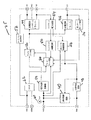
図1は、8ピンの減光バラスト制御用制御回路(IC)25を示し、図4は、ランプ14に給電するバラスト回路内のIC25を示す。IC25は、簡単で高性能の減光バラストの解決案を実現するものである。 FIG. 1 shows an 8-pin dimming ballast control circuit (IC) 25, and FIG. 4 shows an IC 25 in the ballast circuit that supplies power to the lamp 14. The IC 25 implements a simple and high performance dimming ballast solution.
図示の実施例では、8ピンしか有しない集積回路によって、バラスト制御を行っている。VCCピン1は、このICに給電するためのロジック、および内部ゲートドライブパワー電圧VCCを供給する。この電圧は、アンダー電圧ロックアウト(UVLO)回路62およびブートストラップスイッチ52にも与えられる。UVLO回路62は、VCCがスレッショルドレベルを下回ったときに、出力ドライバーステージの作動を防止するためのアンダー電圧ロックアウト保護を行う。 In the illustrated embodiment, ballast control is performed by an integrated circuit having only 8 pins. VCC pin 1 is logic for powering the IC, and The supply an internal gate drive power voltage V CC. This voltage is also applied to an under voltage lockout (UVLO) circuit 62 and a bootstrap switch 52. The UVLO circuit 62 provides under voltage lockout protection to prevent operation of the output driver stage when V CC falls below the threshold level.
ブートストラップ回路52は、電圧VCCを超える電圧レベルVBで、高電圧側ドライバーに給電するための高電圧側ドライバーステージ電圧を発生する。COMピン2は、ICパワーであり、UVLO回路52にも提供される信号のアースである。UVLO回路62からの信号は、フォールトロジック回路66に提供される。 The bootstrap circuit 52 generates a high-voltage side driver stage voltage for supplying power to the high-voltage side driver at a voltage level V B exceeding the voltage V CC . The COM pin 2 is IC power and is the ground for the signal that is also provided to the UVLO circuit 52. The signal from the UVLO circuit 62 is provided to the fault logic circuit 66.
DIMピン3は、減光制御回路40に、減光制御およびフィードバック入力を提供し、減光制御回路40は、電圧制御式発振器58へ信号入力を与える。点弧保護回路48は、DIMピン3からの入力も受信し、減光制御回路40へ出力を与える。DC DIM入力電圧基準20(図4)とACランプ電流フィードバック12(図4)は、一体に結合されており、単一ピンのDIMピン3を、ランプの輝度レベルの減光、およびフィードバック制御をするのに使用できるようにしている。 The DIM pin 3 provides a dimming control and feedback input to the dimming control circuit 40, which provides a signal input to the voltage controlled oscillator 58. The ignition protection circuit 48 also receives an input from the DIM pin 3 and provides an output to the dimming control circuit 40. The DC DIM input voltage reference 20 (FIG. 4) and the AC lamp current feedback 12 (FIG. 4) are combined together to provide a single pin DIM pin 3 for dimming the lamp brightness level and for feedback control. It can be used to do.
VCOピン4は、充電コンデンサ上の電圧からの入力を電圧制御発振回路58へ与え、減光に必要なその回路の作動周波数を制御する。更にこの回路58は、予熱/点弧モードのための周波数スイープ時間を、フォールトロジック回路66に提供することも行う。VCOピン4には、内部電流源ブースト回路60が接続されており、外部コンデンサCPHを充電するようになっている(図4)。 VCO pin 4 provides an input from the voltage on the charging capacitor to voltage controlled oscillator circuit 58 to control the operating frequency of that circuit required for dimming. The circuit 58 also provides a frequency sweep time for the preheat / ignition mode to the fault logic circuit 66. An internal current source boost circuit 60 is connected to the VCO pin 4 so as to charge an external capacitor CPH (FIG. 4).
LOピン5は、低電圧側ハーフブリッジドライバー回路46からのドライバー出力を発生し、このドライバー出力は、バラスト回路の低電圧側スイッチを駆動するように提供される。LOピン5は、UVLOまたはフォールトモード中の再スタートロジック回路54への入力としても設けられている。この入力は、包括的なシャットダウン機能であり、この用途において、ランプが存在することを検出するのに使用される。 The LO pin 5 generates a driver output from the low voltage side half bridge driver circuit 46, which is provided to drive the low voltage side switch of the ballast circuit. The LO pin 5 is also provided as an input to the restart logic circuit 54 during UVLO or fault mode. This input is a comprehensive shutdown function and is used in this application to detect the presence of a lamp.
VSピン6は、出力ハーフブリッジバラスト回路のスイッチングモードVSに結合されており、高電圧側ハーフブリッジのドライバー電圧フローティング供給電圧を受け、ハーフブリッジ電流および電圧検出回路64のための入力を発生する。回路64は、非ゼロ電圧スイッチング(ZVS)保護回路56、およびクレストファクター保護回路50への入力を発生する。バラスト保護機能を実行するためのハーフブリッジ電流、および電圧の単一高電圧VSピン6が検出するようになっている。 The VS pin 6 is coupled to the switching mode VS of the output half bridge ballast circuit, receives the high voltage side half bridge driver voltage floating supply voltage, and generates an input for the half bridge current and voltage detection circuit 64. Circuit 64 generates inputs to non-zero voltage switching (ZVS) protection circuit 56 and crest factor protection circuit 50. A single high voltage VS pin 6 for detecting the half-bridge current and voltage for performing the ballast protection function is detected.
HOピン7は、高電圧側ハーフブリッジドライバー回路44からのドライバー出力を、バラスト回路の高電圧スイッチへ与える。VBピン8は、ブートストラップスイッチ52によって制御された高電圧側ハーフブリッジドライバーのフローティング電圧を発生する。 The HO pin 7 supplies the driver output from the high voltage side half bridge driver circuit 44 to the high voltage switch of the ballast circuit. The VB pin 8 generates a floating voltage of the high voltage side half bridge driver controlled by the bootstrap switch 52.
IC25は、VCCピン1と、COMピン2との間に、ツェナークランプ構造回路(図示せず)を有し、このツェナークランプ回路は、例えば15.6Vの公称ブレーク電圧を有する。この電源は、表3に指定されたVCLAMPよりも大きい低インピーダンスのDC電源の電圧で駆動してはならない。内部の15.6Vのツェナーダイオードが、このピンにおける電圧をクランプする状態を維持するために、VCCピンに十分な電流を供給しなければならない。更に、VSピン6が、アースよりも低い電圧に5Vよりも大きく誘導される出力スイッチング状態は、回避しなければならない。 The IC 25 has a Zener clamp structure circuit (not shown) between the VCC pin 1 and the COM pin 2, and this Zener clamp circuit has a nominal break voltage of 15.6V, for example. This power supply must not be driven by a low impedance DC power supply voltage greater than V CLAMP specified in Table 3. An internal 15.6V Zener diode must supply enough current to the VCC pin in order to keep the voltage at this pin clamped. Furthermore, output switching conditions in which the VS pin 6 is induced greater than 5V to a voltage lower than ground must be avoided.
IC25は、更にドライバーロジック回路42を含み、ドライバーロジック回路42は、VCO58の発振出力信号を入力として受信する。IC25は、更にフォールトロジック回路66からの入力も有する。ドライバーロジック回路42は、高電圧側ハーフブリッジドライバー44、および低電圧側ハーフブリッジドライバー46を制御する。フォールトロジック回路66は、UVLO回路62からの入力の他に、更に再スタートロジック回路54、点弧検出回路48、およびクレストファクター保護回路50からの入力を受け、バラスト保護を行う。 The IC 25 further includes a driver logic circuit 42 that receives the oscillation output signal of the VCO 58 as an input. The IC 25 further has an input from the fault logic circuit 66. The driver logic circuit 42 controls the high voltage side half bridge driver 44 and the low voltage side half bridge driver 46. In addition to the input from the UVLO circuit 62, the fault logic circuit 66 further receives inputs from the restart logic circuit 54, the ignition detection circuit 48, and the crest factor protection circuit 50, and performs ballast protection.
上記のように、IC25は、閉ループランプ電流減光制御回路40と、高電圧側ハーフブリッジドライバー44、および低電圧側ハーフブリッジドライバー46を駆動するドライバーロジック回路42と、点弧検出回路48と、クレストファクター保護回路50と、ブートストラップスイッチ52と、ランプ再スタートロジック回路54と、非ZVS保護を行うための非ZVS保護回路56と、VCC、例えば15.6Vのツェナークランプダイオードとを有する。IC25は、プログラマブルブリヒート時間、固定デッドタイム(1.5μsのタイプ)、例えば200μAのマイクロパワーのスタートアップ、およびラッチイミュニティおよびESD保護も含んでいる。 As described above, the IC 25 includes the closed loop lamp current dimming control circuit 40, the driver logic circuit 42 that drives the high voltage side half bridge driver 44 and the low voltage side half bridge driver 46, the ignition detection circuit 48, It has a crest factor protection circuit 50, a bootstrap switch 52, a lamp restart logic circuit 54, a non-ZVS protection circuit 56 for performing non-ZVS protection, and a Zener clamp diode of V CC , for example, 15.6V. The IC 25 also includes programmable breach time, fixed dead time (1.5 μs type), eg, 200 μA micropower startup, and latch immunity and ESD protection.
図2は、DIMピン3に結合されたIC25内部の回路40を示す。ランプ出力ステージからのフィードバックを使用し、ランプ出力の所望する強度レベルを維持するために、かつデッドタイムのために、DIMピン3における単一入力をどのように使用するかを示している。 FIG. 2 shows circuit 40 inside IC 25 coupled to DIM pin 3. The feedback from the lamp output stage is used to show how to use a single input at DIM pin 3 to maintain the desired intensity level of the lamp output and for dead time.
IC25内部に位置する回路40は、DIMピン3からの入力を受ける比較器200を含んでいる。1対の直列接続されたスイッチ210および212のゲートには、比較器200の出力が接続されている。ここで、第1スイッチ210はPMOSであり、電流ソース208に接続されており、第2スイッチ212は、NMOSであり、電流シンク206に接続されている。一般に約625μAのシンク(放出)電流、および160μAのソース(充電)電流が使用される。これによって、安定した減光に重要な、約4:1のシンク対ソース電流比が決まる。 The circuit 40 located inside the IC 25 includes a comparator 200 that receives an input from the DIM pin 3. The output of the comparator 200 is connected to the gates of a pair of switches 210 and 212 connected in series. Here, the first switch 210 is a PMOS and is connected to the current source 208, and the second switch 212 is an NMOS and is connected to the current sink 206. Generally, a sink (discharge) current of about 625 μA and a source (charge) current of 160 μA are used. This determines a sink to source current ratio of about 4: 1 which is important for stable dimming.
次に、減光制御回路60の作動に対して説明する。この制御回路40は、ランプフィードバックを介して所望する減光レベルをセットし、維持するように機能する。 Next, the operation of the dimming control circuit 60 will be described. This control circuit 40 functions to set and maintain the desired dimming level via lamp feedback.
IC25のDIMピン3は、2つの信号、すなわち、減光入力から抵抗器RD 1M1により外部から提供されるDCレベルのVDIM(一般に減光レベルを設定するために1〜10V DCとなっている)およびランプ電流検出抵抗器RCSの両端に生じる、AC結合コンデンサCFBにより、反結合されたAC信号Ilampを受信する。 The DIM pin 3 of the IC 25 has two signals, ie, a DC level V DIM provided externally by a resistor RD 1M1 from a dimming input (typically 1-10V DC to set the dimming level) ) And the lamp-current sensing resistor RCS, the anti-coupled AC signal Ilamp is received by the AC coupling capacitor CFB.
ピン3おける電圧は、減光電圧VDIM(DCレベル)とランプ電流Ilampを示すAC信号との組み合わせを示し、この電圧は、正弦波204となる。比較器200は、DIMピン3における正弦波204の谷202とCOM(ゼロ)とを比較する。谷202がCOMよりも低下すれば、比較器200は、高レベルの信号を出力し、シンク電流206をVCOピン4に接続している下方のNMOS FET212を、ターンオンする。このシンク電流は、VCOピン4におけるコンデンサCVCO電圧をわずかに放電させ、周波数を高くする。この周波数の増加により、正弦波の振幅(ランプ電流)は若干低下するので、正弦波の谷は、COMよりも上の位置へ上昇する。 The voltage at pin 3 represents a combination of a dimming voltage V DIM (DC level) and an AC signal indicating lamp current Ilamp, which is a sine wave 204. Comparator 200 compares trough 202 of sine wave 204 at DIM pin 3 with COM (zero). If trough 202 falls below COM, comparator 200 outputs a high level signal and turns on the lower NMOS FET 212 that connects sink current 206 to VCO pin 4. This sink current slightly discharges the capacitor CVCO voltage at the VCO pin 4 and increases the frequency. As the frequency increases, the amplitude (lamp current) of the sine wave slightly decreases, and the valley of the sine wave rises to a position above COM.
正弦波の谷202が0よりも高くなった場合、比較器の出力は、低レベルとなり、上部PMOS FET210は、ターンオンし、ソース電流208をVCOピン4に接続する。このソース電流は、VCOピンにおけるコンデンサCVCO電圧を高め、周波数を若干低下させる。これによって、ランプ電流、よって正弦波の振幅が増加し、谷は最終的にCOMレベルの位置まで低下する。従って、回路40は、正弦波の谷202をCOMにするように周波数を常に変えようとしている。 If the sine wave valley 202 goes higher than zero, the comparator output goes low and the upper PMOS FET 210 turns on and connects the source current 208 to the VCO pin 4. This source current increases the capacitor CVCO voltage at the VCO pin and slightly reduces the frequency. This increases the lamp current, and hence the amplitude of the sine wave, and eventually the trough drops to the COM level position. Therefore, the circuit 40 is constantly trying to change the frequency so that the sinusoidal valley 202 is COM.
しかし、谷202がCOMに達するときは、いつも、VCOにシンクパルスが送られ、再び周波数は高くなり、谷はCOMよりも上に上昇する。このようなサイクルを繰り返すたびに、谷は、最終的にCOMとなるように正しく制御され、VCOの電圧は、シンク電流、およびソース電流によって決定される定常状態の値に到達し、ランプの減光レベルを、VDIMによって決定される値に維持する。 However, whenever the valley 202 reaches COM, a sync pulse is sent to the VCO, the frequency goes up again, and the valley rises above COM. Each time such a cycle is repeated, the trough is properly controlled to eventually become COM, and the voltage of the VCO reaches a steady state value determined by the sink and source currents, reducing the ramp. The light level is maintained at a value determined by VDIM.
VCOの電圧は、正しいランプ電流の振幅を定める周波数を設定する。バラストのハーフブリッジ(図4の30参照)は、常に50%のデューティサイクルで作動しているので、ランプ電流が正しいレベルにレギュレートされた状態を維持するように、この周波数を有する固定デッドタイムが制御される。共振出力ステージ(並列RおよびCRESと直列なLRESA)(図4)は、伝達関数、例えば利得と周波数を定める伝達関数を有し、この伝達関数は周波数が低下するにつれ、ランプ電流を増加し、周波数が高まるにつれ、ランプ電流を減少させる。 The voltage of the VCO sets the frequency that determines the correct lamp current amplitude. Since the ballast half-bridge (see 30 in FIG. 4) is always operating at a 50% duty cycle, a fixed dead time with this frequency so that the lamp current remains regulated at the correct level. Is controlled. The resonant output stage (LRESA in series with parallel R and CRES) (FIG. 4) has a transfer function, eg, a transfer function that defines gain and frequency, which increases the lamp current as frequency decreases, As the frequency increases, the lamp current is reduced.
図3は、IC25の状態を示す。まずステップ102において、電源がオンとされると、すなわち、VCCピン12におけるVCCが0よりも大となると、IC25は、ステップ104において、UVLOモードに入る。UVLOモードでは、次の設定が確立する。すなわち、ハーフブリッジ30(図1)がオフとなり、IQCC≒200μAが設定される。VCOピン40は、0Vに等しくなり、HOピン7は、オフとなり、LOピン5は、オープン回路となる。 FIG. 3 shows the state of the IC 25. First, in step 102, when the power is turned on, that is, when V CC at VCC pin 12 becomes greater than 0, IC 25 enters UVLO mode in step 104. In the UVLO mode, the following settings are established. That is, the half bridge 30 (FIG. 1) is turned off, and I QCC ≈200 μA is set. VCO pin 40 is equal to 0V, HO pin 7 is off, and LO pin 5 is an open circuit.
VCCピン1が、12.5V(UVLO+)よりも大となり、LOピン5が、4.7V未満(このことはランプが挿入されたことを意味する)となると、IC25はステップ106において、予熱/点弧モードとなる。IC25が予熱/点弧モードとなっており、ランプが点弧しない間、DIMピンには、AC成分が存在せず、DIM電圧はDCレベルのままとなる。従って、VCOは、4.5Vよりも上の電圧となり、次に、フォールトモードとなり、シャットダウンする。 When VCC pin 1 is greater than 12.5V (UVLO +) and LO pin 5 is less than 4.7V (which means that the lamp has been inserted), IC 25 will preheat / The firing mode is set. While the IC 25 is in preheat / ignition mode and the lamp does not ignite, there is no AC component at the DIM pin and the DIM voltage remains at the DC level. Thus, the VCO is at a voltage above 4.5V, then enters a fault mode and shuts down.
フォールトロジック回路66は、VCOに結合された入力を有する。ランプが点弧すると、IC25の点弧検出回路48は、ランプ電流を検出する。この理由は、約40イベントの間で、DIMピン3における正弦波の谷202は、COMよりも下に低下するからである。 Fault logic circuit 66 has an input coupled to the VCO. When the lamp is ignited, the ignition detection circuit 48 of the IC 25 detects the lamp current. This is because, for approximately 40 events, the sinusoidal valley 202 at the DIM pin 3 falls below COM.
予熱/点弧モードでは、次の設定が確立する。ハーフブリッジの発振周波数は、fMAXからfMINまで、ランプ係数に従って変化する。VCOピン4は、充電され(1μA)、クレストファクターおよび非ZVSは、フォールトディスエーブルされる。更に、DIMピン3が30イベントとの間、0Vよりも下のままであると、IC25は、ステップ108においてDIMモードとなり、IC25は、UVLAモードに戻る。 In the preheat / ignition mode, the following settings are established. The oscillation frequency of the half bridge changes from f MAX to f MIN according to the ramp coefficient. VCO pin 4 is charged (1 μA) and crest factor and non-ZVS are fault disabled. Further, if DIM pin 3 remains below 0V for 30 events, IC 25 enters DIM mode at step 108 and IC 25 returns to UVLA mode.
一旦点弧が検出されると、IC25は、DIMモードに入り、回路40のシンク/ソース減光制御(図2)が附勢される。DIMモード中、ランプを取り外した場合、インダクタが飽和状態となるまで、減光制御ループまたは非ZVSが共振状態を生じさせるように、周波数をレギュレートする。インダクタが飽和すると、インダクタのクレストファクターCF(ピーク対平均値)は、5を超え、これによって、IC25はステップ110においてフォールトモードとなり、シャットダウンする。 Once firing is detected, the IC 25 enters the DIM mode and the sink / source dimming control (FIG. 2) of the circuit 40 is activated. During DIM mode, if the lamp is removed, the frequency is regulated so that the dimming control loop or non-ZVS causes a resonant condition until the inductor is saturated. When the inductor saturates, the crest factor CF (peak to average) of the inductor exceeds 5, which causes the IC 25 to enter the fault mode at step 110 and shut down.
DIMモードでは、次の設定が確立される。ハーフブリッジ発振周波数はfDIMで設定され、減光ループがイネーブルされ、非ZVS保護のクレストファクターがイネーブルされる。 In DIM mode, the following settings are established. The half-bridge oscillation frequency is set by f DIM , the dimming loop is enabled, and the non-ZVS protected crest factor is enabled.
VCCピン1における電圧が、10.5V(UVLO−)未満となると、IC25は、107または109で示されるように、任意の状態からUVLOモードに戻る。非ZVSに対し、IC25は、ステップ112にてZVSモードになり、このモードではUVOピン4の値が減少する。すなわち、VCO=VCO−dVとなり、ハーフブリッジの発振周波数が高くなる。すなわち、freq.=またはfreq.+dfとなり、IC25は、DIMモードに戻る。こうして、ZVSループによりスイッチは、ゼロ電圧スイッチング状態となるように駆動される。 When the voltage at VCC pin 1 is less than 10.5 V (UVLO−), IC 25 returns from any state to UVLO mode, as indicated at 107 or 109. For non-ZVS, the IC 25 enters the ZVS mode at step 112, where the value of the UVO pin 4 decreases. That is, VCO = VCO−dV, and the half-bridge oscillation frequency increases. That is, freq. = Or freq. + Df, and the IC 25 returns to the DIM mode. Thus, the ZVS loop drives the switch to be in a zero voltage switching state.
上記とは異なり、クレストファクターが5よりも大となる(ランプが点弧せず、すなわち取り外されているとき)か、またはVCOが0.85V(非ZVS)未満となると、IC25は、ステップ110において、フォールトモードになる。このフォールトモードには、フォールトラッチがセットされ、ハーフブリッジは、オフとなり、IQCC≒200μAとなり、HOピン7の出力は、オフとなり、LOピン2は、オープン回路となる。 Unlike the above, when the crest factor is greater than 5 (when the lamp is not ignited, i.e. removed), or the VCO is less than 0.85 V (non-ZVS), the IC 25 determines that the step 110 In the fault mode. In this fault mode, the fault latch is set, the half bridge is turned off, I QCC ≈200 μA, the output of the HO pin 7 is turned off, and the LO pin 2 becomes an open circuit.
フォールトモードからVCCピン1上の電圧が、10.5V(UVLO−)未満となるか、またはLOピン5が5Vよりも大となったとき、すなわち、ランプが取り外されたとき、IC25は、UVLOモードに戻る。 When the voltage on VCC pin 1 falls below 10.5V (UVLO-) from fault mode or LO pin 5 is greater than 5V, ie when the lamp is removed, IC25 will Return to mode.
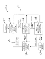
図4は、減光バラスト回路10における本発明のIC25を使用する代表的な応用例を示す。バラスト回路10は、ランプ14からのACフィードバック信号13を、ピン3におけるDC DIM信号に結合する。説明したように、これによって減光、およびフィードバックの双方に対し、単一のICピンを使用することが可能となる。ICランプ電流検出抵抗器は、RC16であり、フィードバック抵抗器RFD、およびコンデンサCFB18により、ACランプ電流信号12は、減光入力20へ結合される。DIM入力20において、DC DIM信号が提供され、この信号は、1〜10ボルトの可変DCレベルを含むことができる。DIM入力20は、抵抗器RDIM2およびRDIM1により形成された分圧回路に提供される。ノイズフィルタリングのために、別のコンデンサCDINが設けられており、このコンデンサは、結合コンデンサCFB18よりも小さくなっている。一般に、コンデンサCFB18は、470nFに等しく、コンデンサCDIMは、1nFに等しい。 FIG. 4 shows a typical application using the IC 25 of the present invention in the dimming ballast circuit 10. Ballast circuit 10 couples AC feedback signal 13 from lamp 14 to the DC DIM signal at pin 3. As explained, this allows the use of a single IC pin for both dimming and feedback. The IC lamp current sensing resistor is RC16, and the AC lamp current signal 12 is coupled to the dimming input 20 by the feedback resistor RFD and the capacitor CFB18. At the DIM input 20, a DC DIM signal is provided, which can include a variable DC level of 1-10 volts. The DIM input 20 is provided to a voltage divider circuit formed by resistors RDIM2 and RDIM1. For noise filtering, another capacitor CDIN is provided, which is smaller than the coupling capacitor CFB18. In general, capacitor CFB18 is equal to 470 nF and capacitor CDIM is equal to 1 nF.
22におけるDC DIM電圧に対し、コンデンサCFB18によりACランプ電流フィードバック信号12が重ねられる。DIMレベル20は、ピークアンプ電流を制御し、フィードバック信号12は、減光レベルを所望する値に維持する。従って、所望の減光レベル(DC)を発生し、ACフィードバック信号12により、減光レベル、すなわち、輝度レベルを所望のレベルに維持するのに、制御IC25の1つのピン、すなわちピン3を使用するだけでよい。 The AC lamp current feedback signal 12 is superimposed by the capacitor CFB 18 on the DC DIM voltage at 22. The DIM level 20 controls the peak amplifier current, and the feedback signal 12 maintains the dimming level at the desired value. Thus, one pin of control IC 25, pin 3, is used to generate the desired dimming level (DC) and to maintain the dimming level, ie, the luminance level, at the desired level by AC feedback signal 12. Just do it.
図4の減光バラスト回路10は、単一の8ピンチップ減光解決方法を使用する簡単なランプ電流減光制御方法を実行する。このバラスト回路10は、ランプ電流を検出するために単一抵抗器しか必要としない。更に、ハーフブリッジと直列となる電流検出抵抗器は、不要である。外側保護回路および外部ブートストラップダイオードも、不要である。更に回路10は、部品数を大幅に低減させ、生産性および信頼性を高める。短時間の設計サイクル時間で使用することが容易でもある。 The dimming ballast circuit 10 of FIG. 4 implements a simple lamp current dimming control method that uses a single 8-pin chip dimming solution. This ballast circuit 10 requires only a single resistor to detect the lamp current. Furthermore, a current sensing resistor in series with the half bridge is not necessary. An outer protection circuit and an external bootstrap diode are also unnecessary. In addition, the circuit 10 significantly reduces the number of parts and increases productivity and reliability. It is also easy to use with a short design cycle time.
表1は、制御IC25の絶対最大定格を示し、また持続限界も示している。この持続限界を超えると、制御IC25が破壊されることがある。すべての電圧パラメータは、COMを基準とする絶対電圧である。すべての電流は、任意のリード線内に対して、正に定義されている。熱抵抗およびパワー放散定格は、実装された基板、および静止空気条件で測定されている。

正しく作動させるために、制御IC25を使用しなければならない範囲内の推奨条件を、表2に示す。
次の表3には、特に指定しない限りVCC=VBS=14V、VS=0V、およびTA=25℃となっているIC25の電気的特性が示されている。この出力電圧および電流(VO およびIO )パラメータは、COMを基準とし、それぞれ、HOおよびLO出力リード線に適用可能である。 Table 3 below shows the electrical characteristics of the IC 25 where VCC = VBS = 14V, VS = 0V, and TA = 25 ° C. unless otherwise specified. This output voltage and current (V O and I O ) parameter is referenced to COM and is applicable to the HO and LO output leads, respectively.
図4の回路10は、ブリッジ整流器R、および入力フィルタEMFだけでなく、DCバスコンデンサCBUSも含むACメイン電源を有している。更に、減光中に低輝度レベルにおいて、安定性を良好にするために、直列抵抗器RVCOおよびコンデンサCPHと並列なVCO充電コンデンサCVCOも含まれている。抵抗器RVCOは、コンデンサCPHの電圧がランプ関数状に増加するにつれ、VCOピン4における電圧がランプ関数状に増加するよう、十分小さい値(約1kオーム)となっている。ランプが点灯するまで、VCOピン4における電圧がランプ関数状に増加するにつれ、周波数は低下する。従って、内部電流ソースを通して充電されるCPHコンデンサは、予熱/点弧タイミングをプログラムしている。CPHとRVCOとの組み合わせは、低輝度レベルでの安定的な減光をするために、減光フィードバックループのための別の補償ネットワークも提供している。 The circuit 10 of FIG. 4 has an AC main power supply that includes a bridge rectifier R and an input filter EMF as well as a DC bus capacitor CBUS. In addition, a VCO charging capacitor CVCO in parallel with the series resistor RVCO and capacitor CPH is also included for better stability at low brightness levels during dimming. Resistor RVCO is sufficiently small (approximately 1 k ohm) so that as the voltage on capacitor CPH increases in a ramp function, the voltage at VCO pin 4 increases in a ramp function. Until the lamp is lit, the frequency decreases as the voltage at the VCO pin 4 increases in a lamp function. Thus, a CPH capacitor charged through an internal current source is programmed with preheat / ignition timing. The combination of CPH and RVCO also provides another compensation network for the dimming feedback loop for stable dimming at low brightness levels.
回路10は、更にVCCフィルタコンデンサCVCCと、ブートストラップ充電コンデンサCBSと、電圧低減抵抗器RVCCト、ゲートドライブ抵抗器RHOおよびRLOと、スナッバーコンデンサCSNUBと、ランプ電圧(再スタート回路54に与えられる)を検出するための電圧検出抵抗器RLMP1、およびRLMP2を有する充電ポンプダイオードDCP1およびDCP2も含んでいる。 The circuit 10 further includes a VCC filter capacitor CVCC, a bootstrap charging capacitor CBS, a voltage reducing resistor RVCC, gate drive resistors RHO and RLO, a snubber capacitor CSNUUB, and a ramp voltage (applied to the restart circuit 54). And charge pump diodes DCP1 and DCP2 having voltage detection resistors RLMP1 and RLMP2 for detecting.
フォールトモードまたはUVLOモード中に、ランプが取り外された場合、下方のランプフィラメント接続部は、オープン回路となり、電圧検出抵抗器RLMP2は、RLMP1を通して、LOピン5を5Vにセットされた内部スレッショルドよりも高い電圧に引き上げる。これによって、IC25は、UVLOモードにホールドされる。フィラメントが再挿入されると、下方のランプフィラメントは、電圧検出抵抗器RLMP1とRLMP2とのノードを、COMの近くのレベルまでとし、よって、LOピン5を4.7Vの内部スレッショルドよりも低い電圧に引き下げ、IC25は、予熱/点弧モードで再スタートする。 If the lamp is removed during fault mode or UVLO mode, the lower lamp filament connection becomes an open circuit, and the voltage sensing resistor RLMP2 passes through RLMP1 above the internal threshold where LO pin 5 is set to 5V. Increase to a higher voltage. As a result, the IC 25 is held in the UVLO mode. When the filament is reinserted, the lower lamp filament brings the node of voltage sensing resistors RLMP1 and RLMP2 to a level near COM, so that LO pin 5 is at a voltage lower than the internal threshold of 4.7V. IC25 is restarted in preheat / ignition mode.
更に、ランプ出力回路は、出力共振インダクアLRESA、LRESBおよびLRESCだけでなく、共振コンデンサCRES、DCブロッキングコンデンサCDCおよびコンデンサCH1、CH2も含んでいる。フィラメントを予熱している間、フィラメントF1、F2は、予熱モード中に与えられる予熱電圧によって加熱される。一旦ランプが起動され、点弧すると、ランプが点灯したときに、ランプの低インピーダンスにより、LRESBおよびCH1、並びにLRESCおよびCH2を含む共振回路がバイパスされる。 Further, the lamp output circuit includes not only the output resonant inductors LRESA, LRESB and LRESC, but also a resonant capacitor CRES, a DC blocking capacitor CDC and capacitors CH1, CH2. While preheating the filaments, the filaments F1, F2 are heated by a preheating voltage applied during the preheating mode. Once the lamp is activated and ignited, the low impedance of the lamp bypasses the resonant circuit including LRESB and CH1, and LRESC and CH2 when the lamp is lit.
以上、本発明の特定の実施例に関連し、本発明について説明したが、当業者には、他の多くの変形例、変更例および他の用途も明らかであると思う。従って、本明細書に記載の特定の開示によって、本発明は限定されるものではない。 Although the present invention has been described with reference to particular embodiments of the present invention, many other variations, modifications, and other uses will be apparent to those skilled in the art. Accordingly, the invention is not limited by the specific disclosures contained herein.
関連出願とのクロスレファレンス
本願は、「減光バラスト制御集積回路」を発明の名称とし、2005年10月24日に出願された米国仮特許出願第60/729,586号に基づく優先権を主張するものであり、この仮特許出願の開示内容を、参考例として援用する。
CROSS REFERENCE WITH RELATED APPLICATIONS This application claims the priority based on US Provisional Patent Application No. 60 / 729,586, filed Oct. 24, 2005, with the title of the invention “dimming ballast control integrated circuit”. The disclosure of this provisional patent application is incorporated as a reference example.
1 VCCピン
2 COMピン
3 DIMピン
5 LOピン
14 ランプ
25 減光バラスト制御IC
40 減光制御回路
46 低電圧側ハーフブリッジドライバー回路
48 点弧保護回路
52 ブートストラップ回路
54 再スタートロジック回路
58 電圧制御式発振器
62 アンダー電圧ロックアウト回路
66 フォールトロジック回路
200 比較器208 電流ソース
210 スイッチ
212 スイッチ
1 VCC pin 2 COM pin 3 DIM pin 5 LO pin 14 Lamp 25 Dimming ballast control IC
40 dimming control circuit 46 low voltage side half bridge driver circuit 48 ignition protection circuit 52 bootstrap circuit 54 restart logic circuit 58 voltage controlled oscillator 62 under voltage lockout circuit 66 fault logic circuit 200 comparator 208 current source 210 switch 212 switch
Claims (23)
バラストパワースイッチング回路の高電圧側スイッチおよび低電圧側スイッチを駆動するためのドライバー回路と、
ランプ給電パルス信号を出力するバラストパワースイッチング回路の作動の周波数を制御するよう、発振信号を発生するための発振回路を備えるドライバー回路を駆動するための制御回路と、
入力を有する減光制御回路とを備え、この減光制御回路は、入力において、ACランプ電流フィードバック信号を受信し、更にこの減光制御回路は、入力においてDC入力電圧基準を受信し、よってDC入力電圧基準は、ランプの所望する減光レベルを決定し、ACランプ電流フィードバック信号は、ランプの輝度を所望する減光レベルに維持するようになっている、減光バラスト制御回路。 In a dimming ballast control circuit for driving a ballast power switching circuit for supplying power to a gas discharge lamp,
A driver circuit for driving the high voltage side switch and the low voltage side switch of the ballast power switching circuit; and
A control circuit for driving a driver circuit including an oscillation circuit for generating an oscillation signal so as to control the frequency of operation of the ballast power switching circuit that outputs the lamp power supply pulse signal;
A dimming control circuit having an input, the dimming control circuit receiving an AC lamp current feedback signal at the input, the dimming control circuit receiving a DC input voltage reference at the input, and thus a DC A dimming ballast control circuit, wherein the input voltage reference determines the desired dimming level of the lamp and the AC lamp current feedback signal is adapted to maintain the lamp brightness at the desired dimming level.
入力を受信し、出力を前記第1および第2スイッチのゲートに与える比較器と、
前記第1および第2スイッチの各々の1つのターミナルに接続された電流ソースおよびシンク回路とを備え、前記第1スイッチと第2スイッチとの間の共通接続部は、前記充電コンデンサに結合されている、請求項4記載の回路。 A first switch and a second switch connected in series;
A comparator that receives an input and provides an output to the gates of the first and second switches;
A current source and sink circuit connected to one terminal of each of the first and second switches, a common connection between the first switch and the second switch being coupled to the charging capacitor; The circuit of claim 4.
低レベルの比較器の出力は、第1スイッチをターンオンし、第1スイッチは、充電コンデンサの電荷を増加させ、ドライバー回路の周波数を低下させ、時間可変信号およびランプ電流の振幅を高め、かつ時間可変信号の谷の電圧レベルを基準レベルよりも低い位置へ低下させ、前記バラストスイッチング回路は、固定されたデューティサイクルで作動するようになっている、請求項8記載の回路。 The high level comparator output turns on the second switch, which discharges the charging capacitor, increases the frequency of the driver circuit, reduces the time variable signal and the lamp current amplitude, and the time variable signal. Raise the voltage level of the valley to a position higher than the reference level,
The low level comparator output turns on the first switch, which increases the charge on the charging capacitor, decreases the frequency of the driver circuit, increases the amplitude of the time variable signal and the lamp current, and the time. 9. The circuit of claim 8, wherein the voltage level of the valley of the variable signal is lowered to a position below the reference level, and the ballast switching circuit is adapted to operate at a fixed duty cycle.
アンダー電圧ロックアウト回路と、
再スタートロジック回路、点弧検出回路、クレストファクター検出回路およびアンダー電圧ロックアウト回路から入力を受信し、出力をドライバー回路に与えるフォールトロジック回路とを備え、
前記発振回路は、前記発振周波数を設定するための入力制御信号(VCO)、および点弧検出回路および減光制御回路からの入力を受信し、前記ドライバー回路を駆動するための発振信号を発生する電圧制御発振器を含む、請求項18記載の回路。 A restart logic circuit for receiving a signal indicating that a lamp is present and generating a shutdown signal if the lamp is not present;
An under voltage lockout circuit;
A fault logic circuit that receives an input from a restart logic circuit, an ignition detection circuit, a crest factor detection circuit, and an under voltage lockout circuit and provides an output to a driver circuit;
The oscillation circuit receives an input control signal (VCO) for setting the oscillation frequency and inputs from an ignition detection circuit and a dimming control circuit, and generates an oscillation signal for driving the driver circuit. The circuit of claim 18 including a voltage controlled oscillator.
Applications Claiming Priority (2)
| Application Number | Priority Date | Filing Date | Title |
|---|---|---|---|
| US72958605P | 2005-10-24 | 2005-10-24 | |
| US11/551,435 US7414372B2 (en) | 2005-10-24 | 2006-10-20 | Dimming ballast control circuit |
Publications (1)
| Publication Number | Publication Date |
|---|---|
| JP2007123271A true JP2007123271A (en) | 2007-05-17 |
Family
ID=37670968
Family Applications (1)
| Application Number | Title | Priority Date | Filing Date |
|---|---|---|---|
| JP2006288266A Pending JP2007123271A (en) | 2005-10-24 | 2006-10-24 | Dimming ballast control circuit |
Country Status (6)
| Country | Link |
|---|---|
| US (1) | US7414372B2 (en) |
| EP (1) | EP1786244B1 (en) |
| JP (1) | JP2007123271A (en) |
| KR (1) | KR100853869B1 (en) |
| AT (1) | ATE406083T1 (en) |
| DE (1) | DE602006002342D1 (en) |
Cited By (2)
| Publication number | Priority date | Publication date | Assignee | Title |
|---|---|---|---|---|
| WO2011149863A2 (en) * | 2010-05-27 | 2011-12-01 | Osram Sylvania Inc. | Dimmer conduction angle detection circuit and system incorporating the same |
| US8410718B2 (en) | 2010-05-27 | 2013-04-02 | Osram Sylvania Inc. | Dimmer conduction angle detection circuit and system incorporating the same |
Families Citing this family (23)
| Publication number | Priority date | Publication date | Assignee | Title |
|---|---|---|---|---|
| JP4516599B2 (en) * | 2005-03-31 | 2010-08-04 | 富士通株式会社 | AC power supply |
| CN101064983B (en) * | 2006-04-27 | 2010-12-15 | 马士科技有限公司 | Compact light-operated florescent lamp and light-operated circuit thereof |
| US7969100B2 (en) * | 2007-05-17 | 2011-06-28 | Liberty Hardware Manufacturing Corp. | Bulb type detector for dimmer circuit and inventive resistance and short circuit detection |
| US8729828B2 (en) * | 2007-06-15 | 2014-05-20 | System General Corp. | Integrated circuit controller for ballast |
| US7855518B2 (en) * | 2007-06-19 | 2010-12-21 | Masco Corporation | Dimming algorithms based upon light bulb type |
| EP2236013A2 (en) * | 2008-01-24 | 2010-10-06 | Osram Gesellschaft mit beschränkter Haftung | Circuit arrangement and method for regulating the current through at least one discharge lamp |
| KR20130088890A (en) * | 2008-04-24 | 2013-08-08 | 인다이스 피티와이 엘티디 | Power control |
| CN201188707Y (en) * | 2008-04-29 | 2009-01-28 | 李金传 | Light modulation control circuit |
| US8358078B2 (en) * | 2008-06-09 | 2013-01-22 | Technical Consumer Products, Inc. | Fluorescent lamp dimmer with multi-function integrated circuit |
| CN101754557A (en) * | 2008-12-08 | 2010-06-23 | 奥斯兰姆有限公司 | Integrated dimmable compact fluorescent lamp and use therein circuit |
| US8212498B2 (en) * | 2009-02-23 | 2012-07-03 | General Electric Company | Fluorescent dimming ballast |
| US8167676B2 (en) * | 2009-06-19 | 2012-05-01 | Vaxo Technologies, Llc | Fluorescent lighting system |
| US8183791B1 (en) | 2009-10-23 | 2012-05-22 | Universal Lighting Technologies, Inc. | System and method for preventing low dimming current startup flash |
| JP5359918B2 (en) * | 2010-02-16 | 2013-12-04 | 三菱電機株式会社 | Semiconductor device |
| JP2013008616A (en) * | 2011-06-27 | 2013-01-10 | Toshiba Lighting & Technology Corp | Luminaire |
| TWI463801B (en) * | 2012-04-26 | 2014-12-01 | Richtek Technology Corp | Zero current detector for a power supplier and method thereof |
| ITVI20120201A1 (en) * | 2012-08-03 | 2012-11-02 | E Z M S R L | DEVICE FOR ADJUSTING THE BRIGHTNESS OF A LAMP, OR DIMMER. |
| EP2696490B1 (en) | 2012-08-09 | 2018-01-10 | Nxp B.V. | AC/DC converter circuit |
| CN105144558B (en) | 2013-04-25 | 2018-06-15 | 三菱电机株式会社 | Charge pump circuit |
| CN103702500A (en) * | 2013-12-10 | 2014-04-02 | 杭州鸿雁东贝光电科技有限公司 | Power control circuit for ballast of fluorescent lamp |
| JP6358840B2 (en) * | 2014-04-24 | 2018-07-18 | シャープ株式会社 | Electric grinder |
| DE102019207981A1 (en) * | 2019-05-31 | 2020-12-03 | Robert Bosch Gmbh | Circuit arrangement with at least one half bridge |
| KR20230152996A (en) * | 2022-04-28 | 2023-11-06 | (주)파인디어칩 | Integrated circuit having power mode setting and individual dimming function |
Family Cites Families (17)
| Publication number | Priority date | Publication date | Assignee | Title |
|---|---|---|---|---|
| US4651060A (en) * | 1985-11-13 | 1987-03-17 | Electro Controls Inc. | Method and apparatus for dimming fluorescent lights |
| US4700111A (en) * | 1986-07-28 | 1987-10-13 | Intelite Inc. | High frequency ballast circuit |
| US5315214A (en) | 1992-06-10 | 1994-05-24 | Metcal, Inc. | Dimmable high power factor high-efficiency electronic ballast controller integrated circuit with automatic ambient over-temperature shutdown |
| US5550436A (en) * | 1994-09-01 | 1996-08-27 | International Rectifier Corporation | MOS gate driver integrated circuit for ballast circuits |
| US5612594A (en) * | 1995-09-13 | 1997-03-18 | C-P-M Lighting, Inc. | Electronic dimming ballast feedback control scheme |
| US5696431A (en) * | 1996-05-03 | 1997-12-09 | Philips Electronics North America Corporation | Inverter driving scheme for capacitive mode protection |
| US5850127A (en) * | 1996-05-10 | 1998-12-15 | Philips Electronics North America Corporation | EBL having a feedback circuit and a method for ensuring low temperature lamp operation at low dimming levels |
| US6008593A (en) * | 1997-02-12 | 1999-12-28 | International Rectifier Corporation | Closed-loop/dimming ballast controller integrated circuits |
| DE69919138T2 (en) | 1998-02-13 | 2005-08-18 | Lutron Electronics Co., Inc. | ELECTRONIC DIMMER |
| US6218788B1 (en) * | 1999-08-20 | 2001-04-17 | General Electric Company | Floating IC driven dimming ballast |
| KR100454278B1 (en) * | 2000-06-19 | 2004-10-26 | 인터내쇼널 렉티파이어 코포레이션 | Ballast control ic with minimal internal and external components |
| US6900599B2 (en) * | 2001-03-22 | 2005-05-31 | International Rectifier Corporation | Electronic dimming ballast for cold cathode fluorescent lamp |
| US6603274B2 (en) * | 2001-04-02 | 2003-08-05 | International Rectifier Corporation | Dimming ballast for compact fluorescent lamps |
| US6366124B1 (en) * | 2001-05-16 | 2002-04-02 | Pericom Semiconductor Corp. | BiDirectional active voltage translator with bootstrap switches for mixed-supply VLSI |
| US6879115B2 (en) * | 2002-07-09 | 2005-04-12 | International Rectifier Corporation | Adaptive ballast control IC |
| US6891339B2 (en) * | 2002-09-19 | 2005-05-10 | International Rectifier Corporation | Adaptive CFL control circuit |
| KR100526240B1 (en) * | 2002-10-09 | 2005-11-08 | 삼성전기주식회사 | Inverter for cold cathode fluorescent lamp of complexing dimming type |
-
2006
- 2006-10-20 US US11/551,435 patent/US7414372B2/en not_active Expired - Fee Related
- 2006-10-23 AT AT06022144T patent/ATE406083T1/en not_active IP Right Cessation
- 2006-10-23 EP EP06022144A patent/EP1786244B1/en not_active Not-in-force
- 2006-10-23 DE DE602006002342T patent/DE602006002342D1/en active Active
- 2006-10-24 JP JP2006288266A patent/JP2007123271A/en active Pending
- 2006-10-24 KR KR1020060103601A patent/KR100853869B1/en active IP Right Grant
Cited By (3)
| Publication number | Priority date | Publication date | Assignee | Title |
|---|---|---|---|---|
| WO2011149863A2 (en) * | 2010-05-27 | 2011-12-01 | Osram Sylvania Inc. | Dimmer conduction angle detection circuit and system incorporating the same |
| WO2011149863A3 (en) * | 2010-05-27 | 2012-04-05 | Osram Sylvania Inc. | Dimmer conduction angle detection circuit and system incorporating the same |
| US8410718B2 (en) | 2010-05-27 | 2013-04-02 | Osram Sylvania Inc. | Dimmer conduction angle detection circuit and system incorporating the same |
Also Published As
| Publication number | Publication date |
|---|---|
| US7414372B2 (en) | 2008-08-19 |
| EP1786244A1 (en) | 2007-05-16 |
| ATE406083T1 (en) | 2008-09-15 |
| US20070090775A1 (en) | 2007-04-26 |
| DE602006002342D1 (en) | 2008-10-02 |
| KR100853869B1 (en) | 2008-08-26 |
| EP1786244B1 (en) | 2008-08-20 |
| KR20070044387A (en) | 2007-04-27 |
Similar Documents
| Publication | Publication Date | Title |
|---|---|---|
| JP2007123271A (en) | Dimming ballast control circuit | |
| US5650694A (en) | Lamp controller with lamp status detection and safety circuitry | |
| KR100858746B1 (en) | Fluorescent ballast controller ic | |
| US7876060B2 (en) | Multi-lamps instant start electronic ballast | |
| US7911153B2 (en) | Electronic ballasts for lighting systems | |
| US8947009B2 (en) | Electronic ballast circuit for lamps | |
| US6127786A (en) | Ballast having a lamp end of life circuit | |
| US7436127B2 (en) | Ballast control circuit | |
| JP2002515173A (en) | Flicker prevention mechanism for ballast driver of fluorescent lamp | |
| JP2000511690A (en) | Triac dimmable compact fluorescent lamp with low power factor | |
| JP2004501600A (en) | Stable control IC with minimal internal and external components | |
| JP2006513555A (en) | Dimming stabilization control IC with flash suppression circuit | |
| US7459867B1 (en) | Program start ballast | |
| US7560868B2 (en) | Ballast with filament heating and ignition control | |
| US6657400B2 (en) | Ballast with protection circuit for preventing inverter startup during an output ground-fault condition | |
| JP2003178895A (en) | Integrated circuit for stable control of closed loop/ illumination control | |
| US7656096B2 (en) | Hybrid ballast control circuit in a simplified package | |
| CN1993006A (en) | Dimming ballast control circuit | |
| JP2008166290A (en) | Hybrid ballast control circuit in simplified package | |
| US8183791B1 (en) | System and method for preventing low dimming current startup flash | |
| JP3034936B2 (en) | Discharge lamp lighting device | |
| KR100865746B1 (en) | Ballast for lamp and method for operating thereof | |
| JP2006092806A (en) | Hybrid ballast control circuit for simplified package |
Legal Events
| Date | Code | Title | Description |
|---|---|---|---|
| A131 | Notification of reasons for refusal |
Free format text: JAPANESE INTERMEDIATE CODE: A131 Effective date: 20090929 |
|
| A02 | Decision of refusal |
Free format text: JAPANESE INTERMEDIATE CODE: A02 Effective date: 20100309 |