Technical domain
-
The present disclosure concerns an electromagnetic compatibility filter for suppressing an unwanted electromagnetic noise component superimposed on an electric supply line. In particular, the present invention concerns an active electromagnetic noise interference (EMI) filter having enhanced performances.
Related art
-
Electric systems in vehicles and in industry are becoming ever more complex and include a multitude of components that generate, or are liable to be disturbed by, electromagnetic interferences. Electric motors, for example, are often driven by electronic inverters that control the motor speed and torque by generating waveforms with variable frequency and amplitude. These systems provide high efficiency but generate a powerful electromagnetic noise.
-
Switching power converters are used in electric and hybrid vehicles, as well as in countless other applications such as driving stationary motors, battery chargers, photovoltaic systems, lighting control, computers, and other. In all these cases, the switching action of the converter is a source of electromagnetic noise that could, if it is not managed or attenuated, affect the functioning of other systems, or exceed normative limits.
-
Electric or electronic filters used to attenuate these unwanted electromagnetic interferences, called EMI filters in short, are used in all branches of electric engineering to improve reliability and respect existing norms. Well-designed filtering system are essential to the performance of many complex electric systems.
-
Electric and hybrid vehicles are equipped with different power converters in a very tight space. This coexistence represents a serious electromagnetic problem and demands efficient EMI filtering. When the filters ae not enough to bring the noise to acceptable levels, shielded cables can be used, but they contribute significantly to costs.
-
It is known to use passive low-pass LC filters to attenuate EMI. While passive solutions do offer substantial attenuation, they have their limits. Magnetic components rated for the current levels used in modern electric vehicles are bulky, expensive, heavy, and not always suitable for mass production.
-
Document
US20180269781 discloses an active EMI filter for an electric vehicle. Active filters can be more compact than equivalent passive ones but providing a satisfactory active filter for the high-current wide-bandwidth interferences generated in electric vehicles is difficult.
-
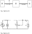
Fig. 1 shows the working principle of an active filter. A load device 21 has a DC bus 15 for conducting the DC main currents. A source device 20 connected to the DC bus 15 with the load device 21 creates noise, in particular EMI. The noise flows on the DC bus 15 in the load device 21 as shown with the solid arrows. Although not shown, the noise flows back to the source device 20 over a ground connection. An active filter 22 between the source device 20 and the load device 21 creates a cancelling noise and injects the cancelling noise in the DC bus 15 to cancel the noise from the source device 20. Consequently, the noise is cancelled by the cancelling noise between the active filter 22 and the load device 21. The cancelling noise flows from the active filter 22 to the load device 21 and then over the ground connection back to the active filter 22.
-
Fig. 2 shows a simple active filter circuit representation implemented as a feedback current-sensing current-injecting circuit, whereby the active filter measures a noise current and injects a cancelling noise current. For the proper functionality, performance and stability of an active filter, the source impedance Zs and the load impedance ZL must be known.
-
The performance, i.e., the attenuation of a feedback current-sensing current-injecting active filter (called insertion loss,
IL), is given by Equation 1:
where A is the filter gain. Equation 1 shows that each of the source impedance Z
S and the load impedance Z
L influences the attenuation of the active filter, such that they must be known and controlled.
-
Since in a real active filter circuit it is not always possible to know or measure exactly the source and load impedances ZS, ZL in the working frequency F W range of the active filter, there is a need to control the source and load impedance ZS, ZL such as to guarantee a stable operation of the active filter. To maximize the attenuation of the feedback current-sensing current-injecting active filter, the source and load impedances ZS, ZL should have the same magnitude ratio over frequency. In this case, the source impedance ZS should be greater than the load impedance ZL.
-
For a voltage-sensing voltage-injecting circuit configuration of the active filter, insertion Loss,
IL is given by Equation 2:
and the attenuation is maximized when the load impedance Z
L is greater than the source impedance Z
S.
Summary
-
An aim of the present invention is the provision of an EMI filter that overcomes the shortcomings and limitations of the state of the art.
-
The present disclosure concerns an EMI filter destined to cooperate with a DC network comprising a source device powering a load device via a DC bus. The EMI filter is connected at an input to the source device and at an output to the load device. The EMI filter comprises an active filter circuit having an active filter bandwidth and being configured to sense a noise component superimposed in the DC bus and inject a cancelling noise in the DC bus to suppress said noise component. The EMI filter further comprises a passive circuit including a source circuit connected at the input and a passive load circuit connected at the output, the passive circuit being configured to provide, at each frequency of the active filter bandwidth, a source impedance at the input that differs from a load impedance at the output by a factor of at least ten times. The passive source circuit is further configured to adjust the magnitude of the noise component such as to avoid saturation of the active filter circuit.
-
The EMI filer disclosed herein provides a minimum, or maximum, impedance magnitude at every working frequency of the active filter bandwidth, so that the desired performance is achieved. The EMI filer guarantees proper functionality of the electronic circuit, without saturation of the circuit and/or instability.
-
The EMI filer can function in different DC networks, without the need of being fine-tuned to each single application, i.e., different converters or different setups having unknown source and load impedances.
-
The EMI filer can further avoid the saturation of the active filter electronic circuit. The EMI filer guarantees a stable and desired values of the source and load impedances, assuring the stability of the EMI filter and increase the performance in the working frequency band.
Short description of the drawings
-
Exemplar embodiments of the invention are disclosed in the description and illustrated by the drawings in which:
- Fig. 1 shows the working principle of an active filter;
- Fig. 2 shows an active filter circuit representation implemented as a feedback current-sensing current-injecting circuit;
- Fig. 3 illustrates an EMI filter comprising a passive circuit, according to an embodiment;
- Fig. 4 illustrates a possible configuration of the passive circuit, according to an embodiment;
- Fig. 5 shows a graph of the source impedance and the load impedance plotted as a function of the working frequency of the active filter circuit of Fig. 4;
- Fig. 6 illustrates a possible configuration of the passive circuit, according to another embodiment;
- Fig. 7 shows a graph of the source impedance and the load impedance plotted as a function of the working frequency of the active filter circuit of Fig. 6; and
- Fig. 8 illustrates the EMI filter, according to another embodiment.
Examples of embodiments
-
With reference to Fig. 3, an EMI filter 22 is shown according to an embodiment. The EMI filter 23 is destined to cooperate with a DC network comprising a source device 20 powering a load device 21 via a DC bus 15. The EMI filter 22 is connected to the source device 20 at an input 23. Here, the term "input" substantially means "at the side of the source device 20". The EMI filter 22 is further connected to the load device 21 at an output 24. Here, the term "output" substantially means "at the side of the load device 21". The EMI filter 22 comprises an active filter circuit 220 having an active filter bandwidth and configured to sense a noise component superimposed in the DC bus 15 and inject a cancelling noise in the DC bus 15 to suppress said noise component.
-
The EMI filter 22 further comprises a passive circuit including a passive source circuit 221 connected at the input 23 and a passive load circuit 222 connected at the output 24. The passive circuit is configured to provide, at each working frequency F W of the active filter bandwidth, a source impedance ZS at the input 23 that differs from a load impedance Z L at the output 24 by a factor of at least ten times.
-
The active filter bandwidth is between 10 kHz and 10 MHz.
-
The passive source circuit 221 can be further configured to adjust the magnitude of the noise component such as to avoid saturation of the active filter circuit 220.
-
In one aspect, the passive source circuit 221 is configured to adjust the magnitude of the noise component below 300 mA. More generally, knowing the noise disturbance coming from the source device 20 and the maximum current/voltage capabilities of the active filter circuit 220, the passive source circuit 221 can be configured to adjust the current/voltage compensation capabilities of the active filter circuit 220, in other words, such that the noise disturbance is reduced in amplitude to fulfil the maximum capabilities of the active filter circuit 220. For example, the passive source circuit 221 can be configured to adjust the magnitude of the noise component by a factor of at least five times. In particular, if the noise coming from the source device 20 has current peaks of 5 A and the active filter circuit 220 can source/sink maximum 1 A, the passive source circuit 221 is designed to reduce the current peaks at least to 1 A.
-
In an embodiment, the active filter circuit 220 comprises a current-sensing current-injecting active filter. The passive circuit 221, 222 is configured such that, at each working frequency F W of the active filter bandwidth, the source impedance ZS is at least 10 times greater than the load impedance Z L.
-
In one aspect, the passive source circuit 221 can include a n-order passive filter, wherein n is 2 or greater.
-
Fig. 4 illustrates a possible configuration of the passive circuit including the source circuit 221 connected at the input 23 and the passive load circuit 222 connected at the output 24, according to an embodiment. As shown if Fig. 4, the passive source circuit 221 can comprise a L-C circuit including at least a source capacitance CS, a source inductance LS and a source damping resistor Rs. For example, the passive source circuit 221 can comprise a L-C circuit including at least a source capacitance CS, a source inductance LS and a source damping resistor Rs connected to the DC bus 15.
-
As shown in Fig. 4, the DC bus 15 can comprise a first power conductor 11 and a second power conductor 12. In such configuration, the L-C circuit including at least a source capacitance CS, a source inductance LS and a source damping resistor Rs can be connected to each of the first and second power conductors 11, 12.
-
In one aspect, the source damping resistor Rs is equal or smaller than 3 Ω.
-
In one aspect, the passive source circuit 221 can comprise a source capacitance CS of about 1 nF and a source inductance LS of about 7 µH.
-
The passive load circuit 222 can include at least a single passive component CL, LL and a load damping resistor RL. For example, the passive load circuit 222 can include at least a single passive component CL, LL and a load damping resistor RL connected to the DC bus 15. As shown in Fig. 4, the DC bus 15 can comprise a first power conductor 11 and a second power conductor 12. In such configuration, the passive load circuit 222 can be connected to each of the first and second power conductors 11, 12.
-
In one aspect, the passive load circuit 222 can include at a load capacitance CL of about 20 nF and a load damping resistor RL of about 1 Ω.
-
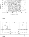
Fig. 5 shows a graph of the source impedance ZS and the load impedance Z L plotted as a function of the working frequency F W of the active filter circuit 220 of Fig. 4. The active filter bandwidth is indicated by the grey area on the graph.
-
In another embodiment, the active filter circuit 220 comprises a voltage-sensing voltage-injecting active filter. The passive load circuit 222 can be configured such that, at each frequency of the active filter bandwidth, a load impedance Z L is at least 10 times greater than the source impedance Zs.
-
Fig. 6 schematically shows an example of such an active filter circuit 220 comprising a voltage-sensing voltage-injecting active filter including a passive source circuit 221 connected at the input 23 and a passive load circuit 222 connected at the output 24. The general description of the circuit is the same as for the current-sensing current-injecting of Fig. 4, i.e., a second or higher order filter at source side and a single component filter at load side. For example, the passive source circuit 221 can comprise a L-C circuit including a source capacitance CS (for example being about 3.3 uF), a source inductance LS (for example being about 100 nH) and a damping resistor Rs smaller than 1 Ohm. The passive load circuit 222 can include a single inductance, e.g., 30 uH. The configuration of the EMI filter 22 shown in Fig. 6 allows for achieving load impedance Z L is at least 10 times greater than the source impedance Z S. in the working frequency of the active filter, i.e., 10 kHz - 10 MHz.
-
Fig. 7 shows a graph of the source impedance Z S and the load impedance Z L plotted as a function of the working frequency F W of the active filter circuit 220 of Fig. 6.
-
The passive circuit 221, 222 is configured to provide, at each frequency of the active filter bandwidth, a source impedance Z S that differs from a load impedance Z L by a factor of at least ten times, and to adjust the magnitude of the noise component such as to avoid saturation of the active filter circuit 220, regardless of the configuration of the active filter 220. For example, the active filter 220 can comprises a current-sensing current-injecting active filter, a voltage-sensing current-injecting active filter, a current-sensing voltage-injecting or a voltage-sensing voltage-injecting active filter.
-
In yet another embodiment, at least one capacitance can be provided between the first and second power conductors 11, 12 between the source device 20 and the EMI filter 22, such as to equalize the impedance seen from each power conductors 11, 12 to ground. In the EMI filter 22 illustrated in Fig. 8, a capacitance C2 is added between the two power conductors 11, 12 on the side of the passive source circuit 221. Here, the passive source circuit 221 and the passive load circuit 222 are similar to the ones shown in Fig. 4.
-
The EMI filter 22 can be placed in a motor drive unit on a DC power bus, in an electric vehicle, although this is not the only application of the present disclosure. Other applications of the EMI filter 22 can include input or output of DC/DC converters and on-board chargers, for example in a vehicle.
Reference numeral used in the figures
-
- 11
- first power conductor
- 12
- second power conductor
- 15
- DC bus
- 20
- source device
- 21
- load device
- 22
- electromagnetic compatibility (EMI) filter
- 220
- active filter circuit
- 221
- passive source circuit
- 222
- passive load circuit
- 223
- passive circuit
- 23
- input
- 24
- output
- A
- filter gain
- BF
- active filter bandwidth
- CL
- load capacitance
- CS
- source capacitance
- C2
- capacitance
- FW
- working frequency
- IL
- insertion Loss
- LL
- load inductance
- LS
- source inductance
- RL
- load damping resistor
- RS
- source damping resistor
- ZS
- source impedance
- ZL
- load impedance