EP4040663A1 - Bidirectional switching converter and operating method thereof - Google Patents
Bidirectional switching converter and operating method thereof Download PDFInfo
- Publication number
- EP4040663A1 EP4040663A1 EP22155678.0A EP22155678A EP4040663A1 EP 4040663 A1 EP4040663 A1 EP 4040663A1 EP 22155678 A EP22155678 A EP 22155678A EP 4040663 A1 EP4040663 A1 EP 4040663A1
- Authority
- EP
- European Patent Office
- Prior art keywords
- offset
- power mosfet
- voltage
- terminal
- time
- Prior art date
- Legal status (The legal status is an assumption and is not a legal conclusion. Google has not performed a legal analysis and makes no representation as to the accuracy of the status listed.)
- Pending
Links
- 230000002457 bidirectional effect Effects 0.000 title claims abstract description 47
- 238000011017 operating method Methods 0.000 title description 2
- 238000001514 detection method Methods 0.000 claims abstract description 17
- 230000005669 field effect Effects 0.000 claims abstract description 5
- 229910044991 metal oxide Inorganic materials 0.000 claims abstract description 5
- 150000004706 metal oxides Chemical class 0.000 claims abstract description 5
- 239000004065 semiconductor Substances 0.000 claims abstract description 5
- 230000004044 response Effects 0.000 claims description 20
- 238000000034 method Methods 0.000 claims description 12
- 230000008859 change Effects 0.000 claims description 8
- 230000003111 delayed effect Effects 0.000 claims description 4
- 230000003247 decreasing effect Effects 0.000 claims description 2
- 238000010586 diagram Methods 0.000 description 16
- 230000006870 function Effects 0.000 description 8
- 238000006243 chemical reaction Methods 0.000 description 6
- 230000003071 parasitic effect Effects 0.000 description 4
- 238000000342 Monte Carlo simulation Methods 0.000 description 3
- 230000003213 activating effect Effects 0.000 description 2
- 230000006872 improvement Effects 0.000 description 2
- 238000004519 manufacturing process Methods 0.000 description 2
- 208000031361 Hiccup Diseases 0.000 description 1
- 239000003990 capacitor Substances 0.000 description 1
- 230000001413 cellular effect Effects 0.000 description 1
- 238000005516 engineering process Methods 0.000 description 1
- 230000002093 peripheral effect Effects 0.000 description 1
- 230000008569 process Effects 0.000 description 1
- 230000007704 transition Effects 0.000 description 1
Images


Classifications
-
- H—ELECTRICITY
- H02—GENERATION; CONVERSION OR DISTRIBUTION OF ELECTRIC POWER
- H02M—APPARATUS FOR CONVERSION BETWEEN AC AND AC, BETWEEN AC AND DC, OR BETWEEN DC AND DC, AND FOR USE WITH MAINS OR SIMILAR POWER SUPPLY SYSTEMS; CONVERSION OF DC OR AC INPUT POWER INTO SURGE OUTPUT POWER; CONTROL OR REGULATION THEREOF
- H02M3/00—Conversion of dc power input into dc power output
- H02M3/02—Conversion of dc power input into dc power output without intermediate conversion into ac
- H02M3/04—Conversion of dc power input into dc power output without intermediate conversion into ac by static converters
- H02M3/10—Conversion of dc power input into dc power output without intermediate conversion into ac by static converters using discharge tubes with control electrode or semiconductor devices with control electrode
- H02M3/145—Conversion of dc power input into dc power output without intermediate conversion into ac by static converters using discharge tubes with control electrode or semiconductor devices with control electrode using devices of a triode or transistor type requiring continuous application of a control signal
- H02M3/155—Conversion of dc power input into dc power output without intermediate conversion into ac by static converters using discharge tubes with control electrode or semiconductor devices with control electrode using devices of a triode or transistor type requiring continuous application of a control signal using semiconductor devices only
- H02M3/156—Conversion of dc power input into dc power output without intermediate conversion into ac by static converters using discharge tubes with control electrode or semiconductor devices with control electrode using devices of a triode or transistor type requiring continuous application of a control signal using semiconductor devices only with automatic control of output voltage or current, e.g. switching regulators
- H02M3/158—Conversion of dc power input into dc power output without intermediate conversion into ac by static converters using discharge tubes with control electrode or semiconductor devices with control electrode using devices of a triode or transistor type requiring continuous application of a control signal using semiconductor devices only with automatic control of output voltage or current, e.g. switching regulators including plural semiconductor devices as final control devices for a single load
- H02M3/1588—Conversion of dc power input into dc power output without intermediate conversion into ac by static converters using discharge tubes with control electrode or semiconductor devices with control electrode using devices of a triode or transistor type requiring continuous application of a control signal using semiconductor devices only with automatic control of output voltage or current, e.g. switching regulators including plural semiconductor devices as final control devices for a single load comprising at least one synchronous rectifier element
-
- H—ELECTRICITY
- H02—GENERATION; CONVERSION OR DISTRIBUTION OF ELECTRIC POWER
- H02M—APPARATUS FOR CONVERSION BETWEEN AC AND AC, BETWEEN AC AND DC, OR BETWEEN DC AND DC, AND FOR USE WITH MAINS OR SIMILAR POWER SUPPLY SYSTEMS; CONVERSION OF DC OR AC INPUT POWER INTO SURGE OUTPUT POWER; CONTROL OR REGULATION THEREOF
- H02M3/00—Conversion of dc power input into dc power output
- H02M3/02—Conversion of dc power input into dc power output without intermediate conversion into ac
- H02M3/04—Conversion of dc power input into dc power output without intermediate conversion into ac by static converters
- H02M3/10—Conversion of dc power input into dc power output without intermediate conversion into ac by static converters using discharge tubes with control electrode or semiconductor devices with control electrode
- H02M3/145—Conversion of dc power input into dc power output without intermediate conversion into ac by static converters using discharge tubes with control electrode or semiconductor devices with control electrode using devices of a triode or transistor type requiring continuous application of a control signal
- H02M3/155—Conversion of dc power input into dc power output without intermediate conversion into ac by static converters using discharge tubes with control electrode or semiconductor devices with control electrode using devices of a triode or transistor type requiring continuous application of a control signal using semiconductor devices only
- H02M3/156—Conversion of dc power input into dc power output without intermediate conversion into ac by static converters using discharge tubes with control electrode or semiconductor devices with control electrode using devices of a triode or transistor type requiring continuous application of a control signal using semiconductor devices only with automatic control of output voltage or current, e.g. switching regulators
- H02M3/158—Conversion of dc power input into dc power output without intermediate conversion into ac by static converters using discharge tubes with control electrode or semiconductor devices with control electrode using devices of a triode or transistor type requiring continuous application of a control signal using semiconductor devices only with automatic control of output voltage or current, e.g. switching regulators including plural semiconductor devices as final control devices for a single load
- H02M3/1582—Buck-boost converters
-
- H—ELECTRICITY
- H02—GENERATION; CONVERSION OR DISTRIBUTION OF ELECTRIC POWER
- H02M—APPARATUS FOR CONVERSION BETWEEN AC AND AC, BETWEEN AC AND DC, OR BETWEEN DC AND DC, AND FOR USE WITH MAINS OR SIMILAR POWER SUPPLY SYSTEMS; CONVERSION OF DC OR AC INPUT POWER INTO SURGE OUTPUT POWER; CONTROL OR REGULATION THEREOF
- H02M3/00—Conversion of dc power input into dc power output
- H02M3/02—Conversion of dc power input into dc power output without intermediate conversion into ac
- H02M3/04—Conversion of dc power input into dc power output without intermediate conversion into ac by static converters
- H02M3/10—Conversion of dc power input into dc power output without intermediate conversion into ac by static converters using discharge tubes with control electrode or semiconductor devices with control electrode
- H02M3/145—Conversion of dc power input into dc power output without intermediate conversion into ac by static converters using discharge tubes with control electrode or semiconductor devices with control electrode using devices of a triode or transistor type requiring continuous application of a control signal
- H02M3/155—Conversion of dc power input into dc power output without intermediate conversion into ac by static converters using discharge tubes with control electrode or semiconductor devices with control electrode using devices of a triode or transistor type requiring continuous application of a control signal using semiconductor devices only
- H02M3/156—Conversion of dc power input into dc power output without intermediate conversion into ac by static converters using discharge tubes with control electrode or semiconductor devices with control electrode using devices of a triode or transistor type requiring continuous application of a control signal using semiconductor devices only with automatic control of output voltage or current, e.g. switching regulators
- H02M3/158—Conversion of dc power input into dc power output without intermediate conversion into ac by static converters using discharge tubes with control electrode or semiconductor devices with control electrode using devices of a triode or transistor type requiring continuous application of a control signal using semiconductor devices only with automatic control of output voltage or current, e.g. switching regulators including plural semiconductor devices as final control devices for a single load
-
- H—ELECTRICITY
- H02—GENERATION; CONVERSION OR DISTRIBUTION OF ELECTRIC POWER
- H02J—CIRCUIT ARRANGEMENTS OR SYSTEMS FOR SUPPLYING OR DISTRIBUTING ELECTRIC POWER; SYSTEMS FOR STORING ELECTRIC ENERGY
- H02J7/00—Circuit arrangements for charging or depolarising batteries or for supplying loads from batteries
- H02J7/0047—Circuit arrangements for charging or depolarising batteries or for supplying loads from batteries with monitoring or indicating devices or circuits
-
- H—ELECTRICITY
- H02—GENERATION; CONVERSION OR DISTRIBUTION OF ELECTRIC POWER
- H02J—CIRCUIT ARRANGEMENTS OR SYSTEMS FOR SUPPLYING OR DISTRIBUTING ELECTRIC POWER; SYSTEMS FOR STORING ELECTRIC ENERGY
- H02J7/00—Circuit arrangements for charging or depolarising batteries or for supplying loads from batteries
- H02J7/0063—Circuit arrangements for charging or depolarising batteries or for supplying loads from batteries with circuits adapted for supplying loads from the battery
-
- H—ELECTRICITY
- H02—GENERATION; CONVERSION OR DISTRIBUTION OF ELECTRIC POWER
- H02J—CIRCUIT ARRANGEMENTS OR SYSTEMS FOR SUPPLYING OR DISTRIBUTING ELECTRIC POWER; SYSTEMS FOR STORING ELECTRIC ENERGY
- H02J7/00—Circuit arrangements for charging or depolarising batteries or for supplying loads from batteries
- H02J7/007—Regulation of charging or discharging current or voltage
- H02J7/00712—Regulation of charging or discharging current or voltage the cycle being controlled or terminated in response to electric parameters
-
- H—ELECTRICITY
- H02—GENERATION; CONVERSION OR DISTRIBUTION OF ELECTRIC POWER
- H02M—APPARATUS FOR CONVERSION BETWEEN AC AND AC, BETWEEN AC AND DC, OR BETWEEN DC AND DC, AND FOR USE WITH MAINS OR SIMILAR POWER SUPPLY SYSTEMS; CONVERSION OF DC OR AC INPUT POWER INTO SURGE OUTPUT POWER; CONTROL OR REGULATION THEREOF
- H02M1/00—Details of apparatus for conversion
- H02M1/0003—Details of control, feedback or regulation circuits
- H02M1/0009—Devices or circuits for detecting current in a converter
-
- H—ELECTRICITY
- H02—GENERATION; CONVERSION OR DISTRIBUTION OF ELECTRIC POWER
- H02M—APPARATUS FOR CONVERSION BETWEEN AC AND AC, BETWEEN AC AND DC, OR BETWEEN DC AND DC, AND FOR USE WITH MAINS OR SIMILAR POWER SUPPLY SYSTEMS; CONVERSION OF DC OR AC INPUT POWER INTO SURGE OUTPUT POWER; CONTROL OR REGULATION THEREOF
- H02M1/00—Details of apparatus for conversion
- H02M1/0003—Details of control, feedback or regulation circuits
- H02M1/0038—Circuits or arrangements for suppressing, e.g. by masking incorrect turn-on or turn-off signals, e.g. due to current spikes in current mode control
-
- H—ELECTRICITY
- H02—GENERATION; CONVERSION OR DISTRIBUTION OF ELECTRIC POWER
- H02M—APPARATUS FOR CONVERSION BETWEEN AC AND AC, BETWEEN AC AND DC, OR BETWEEN DC AND DC, AND FOR USE WITH MAINS OR SIMILAR POWER SUPPLY SYSTEMS; CONVERSION OF DC OR AC INPUT POWER INTO SURGE OUTPUT POWER; CONTROL OR REGULATION THEREOF
- H02M1/00—Details of apparatus for conversion
- H02M1/0048—Circuits or arrangements for reducing losses
- H02M1/0054—Transistor switching losses
- H02M1/0058—Transistor switching losses by employing soft switching techniques, i.e. commutation of transistors when applied voltage is zero or when current flow is zero
-
- H—ELECTRICITY
- H02—GENERATION; CONVERSION OR DISTRIBUTION OF ELECTRIC POWER
- H02M—APPARATUS FOR CONVERSION BETWEEN AC AND AC, BETWEEN AC AND DC, OR BETWEEN DC AND DC, AND FOR USE WITH MAINS OR SIMILAR POWER SUPPLY SYSTEMS; CONVERSION OF DC OR AC INPUT POWER INTO SURGE OUTPUT POWER; CONTROL OR REGULATION THEREOF
- H02M1/00—Details of apparatus for conversion
- H02M1/08—Circuits specially adapted for the generation of control voltages for semiconductor devices incorporated in static converters
- H02M1/083—Circuits specially adapted for the generation of control voltages for semiconductor devices incorporated in static converters for the ignition at the zero crossing of the voltage or the current
-
- H—ELECTRICITY
- H02—GENERATION; CONVERSION OR DISTRIBUTION OF ELECTRIC POWER
- H02M—APPARATUS FOR CONVERSION BETWEEN AC AND AC, BETWEEN AC AND DC, OR BETWEEN DC AND DC, AND FOR USE WITH MAINS OR SIMILAR POWER SUPPLY SYSTEMS; CONVERSION OF DC OR AC INPUT POWER INTO SURGE OUTPUT POWER; CONTROL OR REGULATION THEREOF
- H02M1/00—Details of apparatus for conversion
- H02M1/08—Circuits specially adapted for the generation of control voltages for semiconductor devices incorporated in static converters
- H02M1/088—Circuits specially adapted for the generation of control voltages for semiconductor devices incorporated in static converters for the simultaneous control of series or parallel connected semiconductor devices
Definitions
- the inventive concepts relate to a converter, and more particularly, to a bidirectional switching converter and/or an operating method of the bidirectional switching converter.
- Mobile electronic devices may be driven by battery devices included therein. According to an increase in power consumption of the electronic devices, battery capacity has been increased, and thus, batteries may be charged at various speeds according to magnitudes of voltages supplied by chargers, such as a fast charging method or a general charging method.
- the inventive concepts provide a bidirectional switching converter capable of tracking in real time a point in time when an inductor current is zero.
- a bidirectional switching converter including a first power MOSFET connecting an input voltage node to a switching node, a second power MOSFET connecting the switching node to a ground node, and a zero current detection (ZCD) auto-calibration circuit configured to perform one of an operation of generating a first offset for varying a turn-on time of the first power MOSFET according to an operation mode and an operation of generating a second offset for varying a turn-on time of the second power MOSFET according to the operation mode, wherein the ZCD auto-calibration circuit may vary one of a value of the first offset and a value of the second offset, based on a differential value of a voltage of the switching node and a forward-bias detection result.
- ZCD zero current detection
- an electronic device including a battery, a bidirectional switching converter including a first power MOSFET connecting an input voltage node to a switching node, a second power MOSFET connecting the switching node to a ground node, and a zero current detection (ZCD) auto-calibration circuit configured to perform one of an operation of generating a first offset for varying a turn-on time of the first power MOSFET according to an operation mode and an operation of generating a second offset for varying a turn-on time of the second power MOSFET according to the operation mode, a first interface providing the battery with a power supplied from an external device, and a second interface providing the external device with a power output from the battery, wherein the ZCD auto-calibration circuit may change one of a value of the first offset and a value of the second offset, based on a differential value of a voltage of the switching node and a forward-bias detection result.
- ZCD zero current detection
- a method of operating a bidirectional switching converter including setting an initial offset, identifying an operation mode of the bidirectional switching converter, determining whether a forward bias voltage is detected between a first terminal and a second terminal of a first power MOSFET or between a first terminal and a second terminal of a second power MOSFET, according to the identified operation mode, and determining whether an absolute value of a differential value of a voltage of a switching node is greater than a threshold when the forward bias voltage is not detected, wherein the first power MOSFET may connect an input voltage node to the switching node, and the second power MOSFET may connect the switching node to a ground node.
- the turn-off time of one of the first power MOSFET and the second power MOSFET may be varied depending on a differential value of a voltage of the switching node and a forward-bias detection result. For instance, the turn-off time may be moved earlier in response to the differential value exceeding a first threshold. Equally, the turn-off time may be moved earlier in response to the forward bias voltage being detected.
- the turn-off time of one of the first power MOSFET and the second power MOSFET may be varied by changing a value of a respective (first or second) offset. Increasing an offset moves a turn-off time of the respective MOSFET earlier in time. Decreasing the offset moves the turn-off time of the respective MOSFET later in time.
- FIG. 1 is a block diagram schematically illustrating an electronic device including a charger integrated circuit according to an example embodiment of the inventive concepts.
- an electronic device 10 may include a charger integrated circuit (IC) 100 and a battery 200.
- the electronic device 10 may further include a main processor and peripheral devices.
- the electronic device 10 may include a mobile device such as a smartphone, a tablet personal computer (PC), a cellular phone, a personal digital assistant (PDA), a laptop, a wearable device, a global positioning system (GPS) device, an e-book terminal, a digital broadcasting terminal, a motion picture experts group (MPEG) layer-3 (MP3) player, or a digital camera.
- the electronic device 10 may include an electric vehicle.
- the battery 200 may be mounted in the electronic device 10. In one embodiment, the battery 200 may be detachable from the electronic device 10.
- the battery 200 may include one or a plurality of battery cells. The plurality of battery cells may be connected in series or in parallel to each other. When an external charging device is not connected to the electronic device 10, the battery 200 may supply power to the electronic device 10.
- the charger IC 100 may charge the battery 200 and may be referred to as a "battery charger". In addition, the charger IC 100 may supply power to an external device (for example, a wired interface or a wireless interface) connected to the charger IC 100 based on a voltage charged in the battery 200.
- the charger IC 100 may be implemented as an integrated circuit chip and may be mounted on a printed circuit board.
- the charger IC 100 may include a bidirectional switching converter 110 and a charging controller 120.
- the bidirectional switching converter 110 may be implemented as a direct current (DC)-DC converter and may generate an output voltage by dropping or boosting an input voltage.
- DC direct current
- a first power path may be formed in a first direction
- boosting the input voltage that is, during a boost conversion operation
- a second power path may be formed in a second direction opposite to the first direction.
- the bidirectional switching converter 110 may operate in a buck mode (also referred to as buck single mode), a boost mode (or referred to as boost single mode), or a buck-boost mode (also referred to as buck-boost combined mode).
- a buck mode also referred to as buck single mode
- boost single mode or referred to as boost single mode
- buck-boost mode also referred to as buck-boost combined mode
- the bidirectional switching converter 110 may boost an input voltage by performing a buck conversion operation through a first switching operation and may charge the battery 200 based on the boosted voltage.
- the bidirectional switching converter 110 may drop a voltage input from the battery 200 by performing a boost conversion operation through a second switching operation and may supply power to an external device based on the dropped voltage.
- the bidirectional switching converter 110 may perform the buck conversion operation or the boost conversion operation through a third switching operation according to a load current. In the buck-boost mode, the bidirectional switching converter 110 may charge the battery 200 or supply power to an external device.
- the charging controller 120 may perform mode switching between a plurality of charging modes of the bidirectional switching converter 110, for example, a buck mode, a boost mode, and a buck-boost mode and may control a switching operation of the bidirectional switching converter 110 such that a voltage level of an output voltage is the same as or similar to a target voltage level in the plurality of charging modes.
- the charging controller 120 may receive a sensing current and a sensing voltage from the bidirectional switching converter 110 and may generate a control signal and a switching signal switching for controlling a switching operation in each charging mode of the bidirectional switching converter 110 based on the sensing current and the sensing voltage.
- the charger IC 100 may support at least one of various functions such as an under-voltage lockout (UVLO) function, an over-current protection (OCP) function, an over-voltage protection (OVP) function, a soft-start function of reducing an inrush current, a foldback current limit function, a Hiccup Mode function for short circuit protection, and an over-temperature protection (OTP) function so as to properly operate even under a power saving condition.
- UVLO under-voltage lockout
- OCP over-current protection
- OVP over-voltage protection
- soft-start function of reducing an inrush current a foldback current limit function
- Hiccup Mode function for short circuit protection a Hiccup Mode function for short circuit protection
- OTP over-temperature protection
- the electronic device 10 may support wired charging and wireless charging and may include a first power interface 310 and a second power interface 320 for the wired charging and the wireless charging.
- the first power interface 310 may be implemented as a wired power interface and may include a wired charging circuit.
- the second power interface 320 may be implemented as a wireless power interface and may include a wireless charging circuit.
- the charger IC 100 may receive a first input voltage CHGIN from the first power interface 310 and/or a second input voltage WCIN from the second power interface 320 and may charge the battery 200 based on the first input voltage CHGIN and/or the second input voltage WCIN in the buck mode.
- the charger IC 100 may provide power to the first power interface 310 and/or the second power interface 320 based on a voltage of the battery 200 in the boost mode.
- the charger IC 100 may receive the first input voltage CHGIN from the first power interface 310 or the second input voltage WCIN from the second power interface 320, charge the battery 200 based on the first input voltage CHGIN or the second input voltage WCIN, and provide power to the second power interface 320 or the first power interface 310 based on the first input voltage CHGIN or the second input voltage WCIN in the buck-boost mode.
- the charger IC 100 may provide power to the second power interface 320 based on the first input voltage CHGIN and a voltage of the battery 200 or may provide power to the first power interface 310 based on the second input voltage WCIN and the voltage of the battery 200.
- a travel adapter (TA) or an auxiliary battery may be electrically connected to the first power interface 310.
- the TA may convert alternate current (AC) voltages 110 V to 220 V, which are commercial voltages, or voltages supplied from another power supply (for example, a computer) into DC voltages required for charging the battery 200 and provide the DC voltages to the electronic device 10.
- the charger IC 100 may charge the battery 200 or provide power to the second power interface 320 by using the first input voltage CHGIN received from the TA, the auxiliary battery, or so on in the buck mode.
- an on-the-go (OTG) device for example, an OTG Universal Serial Bus (USB) device and so on
- OTG OTG Universal Serial Bus
- the charger integrated circuit 310 may provide power to the OTG device through the first power interface 310.
- the bidirectional switching converter 310 may provide power to the OTG device based on a voltage of the battery 200 in the boost mode or may provide power to the OTG device in the buck mode while charging the battery 200 based on the second input voltage WCIN from the second power interface 320.
- the electronic device 10 supports wired and wireless charging
- the charger IC 100 has to operate in a plurality of charging modes including the buck mode, the boost mode, and the buck-boost mode to support wired charging and/or wireless charging, wired charging-wireless power supply, and wireless charging-wired power supply, and even when an input power supply is unstable, a seamless mode transition between the buck mode, the boost mode, and the buck-boost mode is required for stable wireless power supply or stable wired power supply.
- FIG. 2 is a diagram of a bidirectional switching converter 110 according to an example embodiment of the inventive concepts.
- the bidirectional switching converter 110 may include a first power metal oxide semiconductor field effect transistor (MOSFET) 210, a second power MOSFET 220, a pulse width modulation (PWM) controller 230, and a zero current detection (ZCD) auto-calibration circuit 240.
- MOSFET metal oxide semiconductor field effect transistor
- PWM pulse width modulation
- ZCD zero current detection
- the PWM controller 230 may output a first control signal PWM_HS and a second control signal PWM_LS.
- the first control signal PWM_HS may include a control signal for turning on/off the first power MOSFET 210.
- the second control signal PWM LS may include a control signal for turning on/off the second power MOSFET 220.
- the PWM controller 230 may adjust an output ratio between the first control signal PWM_HS and the second control signal PWM_LS in response to a mode signal MODE instructing an operation mode.
- the first power MOSFET 210 may be referred to as a high side (HS) switching device
- the second power MOSFET 220 may be referred to as a low side (LS) switching device.
- the first control signal PWM HS and the second control signal PWM_LS may be pulse width modulated signals.
- the ZCD auto-calibration circuit 240 may adjust in real time an offset value for detecting a zero current of a switching node LX.
- the ZCD auto-calibration circuit 240 may reduce or increase the offset value based on a differential value of the switching node LX and a detection result of a diode detector 243.
- the second power MOSFET 220 may be turned off before a switching current I_IND flowing through the switching node LX is zero.
- the ZCD auto-calibration circuit 240 may reduce the offset value to delay a point in time when the second power MOSFET 220 is turned off.
- the second power MOSFET 220 may be turned off after the switching current I_IND flowing through the switching node LX is zero.
- the ZCD auto-calibration circuit 240 may increase the offset value to move up (e.g. move earlier) the point in time when the second power MOSFET 220 is turned off. Detailed operations of the ZCD auto-calibration circuit 240 are described below.
- the ZCD auto-calibration circuit 240 may further include a differentiator 241, a comparator 242, and a diode detector 243.
- the differentiator 241 may differentiate a voltage value of the switching node LX and output a result value to the comparator 242.
- the result value may be obtained by differentiating the voltage value of the switching node LX and taking an absolute value thereof.
- the differentiator 241 may include a capacitor for generating a differential current of the switching current I IND, a mirror circuit for copying the generated differential current, and a resistor for converting a copied differential current into a voltage in order to differentiate the voltage value of the switching node LX.
- the comparator 242 may receive a differential value from the differentiator 241 and compare the differential value with a threshold. When the result value is greater than the threshold, the comparator 242 may output a control signal instructing to increase a count value (e.g. increase the offset) to the counter 244. When the result value is less than the threshold, the comparator 242 may output a control signal instructing to maintain the count value to the counter 244.
- the diode detector 243 may detect a current direction of the switching current I_IND flowing through the switching node LX. In the buck mode, the diode detector 243 may compare a voltage of the switching node LX and a voltage of a ground node, which are both ends (i.e. a first terminal and a second terminal, respectively) of the second power MOSFET 220 in the buck mode, to detect whether a forward bias voltage is applied thereto.
- the diode detector 243 may compare a voltage of the input voltage node VIN and a voltage of the switching node LX, which are both ends (i.e., a first terminal and a second terminal, respectively) of the first power MOSFET 210, to detect whether a forward bias voltage is applied thereto.
- the diode detector 243 may generate a control signal for reducing an offset (e.g. decrease the counter) in response to detection of the forward bias voltage and transmit the control signal to the counter 244.
- the counter 244 may adjust an offset value based on the control signal received from the differentiator 241 and the diode detector 243.
- the counter 244 may receive an up-control signal from the comparator 242 while operating in the buck mode.
- the up-control signal received from the comparator 242 may be a signal requesting to increase an offset value.
- the counter 244 may also receive a down-control signal from the diode detector 243.
- the down-control signal may be a signal requesting to increase an offset value.
- the ZCD auto-calibration circuit 240 may receive a mode signal MODE and output the adjusted offset value according to an operation mode. For example, when the ZCD auto-calibration circuit 240 receives the mode signal MODE indicating the buck mode, an offset value may be output to a buck comparator 250. In another example, when the ZCD auto-calibration circuit 240 receives the mode signal MODE indicating the boost mode, the offset value may be output to a boost comparator 260.
- a turn-on ratio or a turn-off ratio of the first power MOSFET 210 may vary according to the first control signal PWM_HS and a result of comparison performed by the boost comparator 260 based on the switching node LX and the offset value.
- a turn-on ratio or a turn-off ratio of the second power MOSFET 220 may vary according to the second control signal PWM_LS and a result of comparison performed by the buck comparator 250 based on the switching node LX and the offset value.
- the turn-on ratios and turn-off ratios of the first power MOSFET 210 and the second power MOSFET 220 may vary, and thus, a turn-off time of the first power MOSFET 210 and a turn-off time of the second power MOSFET 220 may also vary.
- FIG. 3A is a timing diagram illustrating when a point in time when the second power MOSFET 220 is turned off is earlier than a point in time when the switching current I_IND is zero in the buck mode according to example embodiments of the inventive concepts.
- the switching current I_IND may flow in a forward direction.
- the forward direction may be a direction in which a current flows to the battery 200.
- the switching current I_IND may have a positive value when the switching current I_IND flows in the forward direction.
- the second power MOSFET 220 may be turned off when a gate signal GD_LS is transitioned to a logic low level.
- a check signal may be generated at a falling edge of the gate signal GD_LS.
- the check signal may be an impulse signal applied to a gate of the second power MOSFET 220.
- a voltage of the switching node LX may change according to a current direction of the switching current I IND at a point in time when the check signal is generated. Referring to FIG.
- the gate signal GD_LS of the second power MOSFET 220 may be transitioned to a logic low level at a point in time T1 to generate a check signal.
- the switching current I_IND may be zero at a point in time T2. That is, the second power MOSFET 220 may be first turned off before the switching current I IND is zero (T2 may be later than T1). In a case where the switching current I_IND flows in the forward direction when the second power MOSFET 220 is turned off, the switching current I IND may flow through a body diode of the second power MOSFET 220.
- the ZCD auto-calibration circuit 240 may reduce an offset value to delay a point in time when the gate signal GD_LS of the second power MOSFET 220 is transitioned to a logic low level.
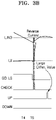
- FIG. 3B is a timing diagram illustrating when a point in time when the second power MOSFET 220 is turned off is later than a point in time when the switching current I IND is zero in the buck mode, according to an example embodiment of the inventive concepts.
- the switching current I IND may flow in a reverse direction.
- the reverse direction may be a direction in which a current flows from the battery 200.
- the switching current I IND may have a negative value when flowing in the reverse direction.
- the switching current I_IND may be zero at a point in time T4.
- the gate signal GD_LS of the second power MOSFET 220 may be transitioned to a logic low level at a point in time T5 to generate a check signal. That is, the second power MOSFET 220 may be turned off after the switching current I_IND is zero (T5 may be later than T4).
- a voltage of the switching node LX may rapidly increase. Because the voltage of the switching node LX rapidly increases, a differential value of the voltage of the switching node LX may be great enough to be greater than a threshold. When the differential value of the voltage of the switching node LX is greater than the threshold, the ZCD auto-calibration circuit 240 may increase an offset value to move up (e.g. bring forward) a point in time when the gate signal GD_LS of the second power MOSFET 220 is transitioned to a logic low level.
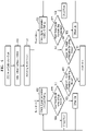
- FIG. 4 is a flowchart illustrating a method of operating the ZCD auto-calibration circuit according to an example embodiment of the inventive concepts.
- the ZCD auto-calibration circuit 240 may set an initial offset value during operation 410.
- the initial offset value may be a preset value during a manufacturing process. However, an environment of the manufacturing process and an operating environment may change depending on process, voltage, temperature (PVT) variation. Due to the PVT variation, a point in time when the second power MOSFET 220 is turned off according to the initial offset value may not be same with a point in time when the switching current I IND is zero.
- a point in time when the second power MOSFET 220 is turned off according to the initial offset value may not be same with a point in time when the switching current I IND is zero according to a voltage of the battery 200 in a fully charged state and a voltage of the battery 200 in a discharged state.
- the ZCD auto-calibration circuit 240 may determine whether an operation mode is a buck mode or a boost mode. For example, the ZCD auto-calibration circuit 240 may receive the mode signal MODE from the charging controller 120. For example, when the bidirectional switching converter 110 supports the buck mode and the boost mode, the mode signal MODE may be 1 bit. The ZCD auto-calibration circuit 240 may identify that the boost mode is indicated when the mode signal MODE is in a logic high level and the buck mode is indicated when the mode signal MODE is in a logic low level.
- the ZCD auto-calibration circuit 240 may generate a check signal when the first power MOSFET 210 is turned off. Operation 430 may be implemented in response to the ZCD auto-calibration circuit 240 determining that the operation mode is the boost mode in operation 420.
- the ZCD auto-calibration circuit 240 may monitor on/off of the first power MOSFET 210 based on the boost mode.
- the ZCD auto-calibration circuit 240 may generate a check signal when the first power MOSFET 210 is turned off.
- the check signal may include a control signal for activating the differentiator 241 to measure the differential value of the voltage of the switching node LX.
- the ZCD auto-calibration circuit 240 may determine whether a forward bias voltage is detected by the diode detector 243. When a point in time when the first power MOSFET 210 is turned off is earlier than a point in time when the switching current I_IND is zero, the switching current I_IND may flow to the diode detector 243. Thus, the diode detector 243 may detect a forward bias voltage. In this case, the forward bias voltage may be a positive voltage. When the forward bias voltage is detected, the counter 244 may reduce an offset value. As the offset value is reduced, a time interval during which the first power MOSFET 210 is turned off may be reduced (e.g. the point in time at which the first power MOSFET 210 is first turned off may be delayed).
- This may reduce the time interval between the point in time point when the switching current I IND is zero and the point in time when the first power MOSFET 210 is turned off. As the time interval during which the first power MOSFET 210 is turned off is reduced, the forward bias voltage detected by the diode detector 243 may also be gradually reduced. When the forward bias voltage is not detected by the diode detector 243, the ZCD auto-calibration circuit 240 may proceed to operation 440.
- the ZCD auto-calibration circuit 240 may determine whether the differential value of the voltage of the switching node LX is greater than a threshold. For example, the point in time when the first power MOSFET 210 is turned off may be later than the point in time when the switching current I_IND is zero. When the first power MOSFET 210 is turned off, the switching current I_IND may flow to the battery 200. While the switching current I_IND flows into the battery 200 to charge the battery 200, a voltage of the switching node LX may be reduced.
- a magnitude of the switching current I IND flowing into the battery 200 may depend on a magnitude of a slope at which the voltage of the switching node LX is reduced. That is, as the magnitude of the switching current I IND flowing into the battery 200 increases, the voltage of the switching node LX may be rapidly reduced.
- the comparator 242 may determine that a differential value output from the differentiator 241 is greater than a threshold. In this case, the differential value may be a negative value. As an absolute value of the differential value is greater than the threshold, the counter 244 may increase the offset value.
- the ZCD auto-calibration circuit 240 may also first determine whether a differential value is greater than a threshold in operation 440 or may also simultaneously perform operation 435 and operation 440. That is, operations 440 and 435 may be performed in any order or may be performed simultaneously (in parallel).
- the ZCD auto-calibration circuit 240 may generate a check signal when the second power MOSFET 220 is turned off. Operation 450 may be performed in response to the ZCD auto-calibration circuit 240 determining that the operation mode is the buck mode in operation 420.
- the ZCD auto-calibration circuit 240 may monitor on/off of the second power MOSFET 220 based on the buck mode.
- the ZCD auto-calibration circuit 240 may generate a check signal when the second power MOSFET 220 is turned off.
- the check signal may be a control signal for activating the differentiator 241 to measure a differential value of a voltage of the switching node LX.
- the ZCD auto-calibration circuit 240 may determine whether a forward bias voltage is detected by the diode detector 243.
- the switching current I_IND may flow to the diode detector 243.
- diode detector 243 may detect the forward bias voltage.
- the forward bias voltage may be a negative voltage.
- the counter 244 may reduce an offset value. As the offset value is reduced, a time interval during which the second power MOSFET 220 is turned off may be reduced (e.g. the point in time at which the second power MOSFET 220 is first turned off may be delayed).
- This may reduce a time interval between the point in time point when the switching current I_IND is zero and the point in time when the second power MOSFET 220 is turned off. As the time interval during which the second power MOSFET 220 is turned off is reduced, a magnitude of the forward bias voltage detected by the diode detector 243 may be gradually reduced. When the forward bias voltage is not detected by the diode detector 243, the ZCD auto-calibration circuit 240 may proceed to operation 460.
- a magnitude of the switching current I_IND output from the battery 200 may depend on a magnitude of a slope at which the voltage of the switching node LX increases. That is, as the magnitude of the switching current I IND output from the battery 200 increases, the voltage of the switching node LX may rapidly increase.
- the comparator 242 may determine that a differential value output from the differentiator 241 is greater than a threshold. In this case, the differential value may be a positive value. As an absolute value of the differential value is greater than the threshold, the counter 244 may increase the offset value.
- the voltage of the switching node LX may be slowly reduced by LC resonance due to parasitic capacitances of the inductor and the switching node LX.
- the counter 244 may maintain the offset value when the voltage of the switching node LX is slowly reduced by the LC resonance and the absolute value of the differential value is less than the threshold.
- the ZCD auto-calibration circuit 240 may also first determine whether a differential value is greater than a threshold in operation 460 or may also simultaneously perform operation 455 and operation 460. That is, operations 455 and 460 may be performed in any order or may be performed simultaneously (in parallel).
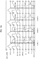
- FIG. 5A is a timing diagram according to an operation of the ZCD auto-calibration circuit 240 in a buck mode, according to an example embodiment of the inventive concepts.
- the bidirectional switching converter 110 may operate in the buck mode.
- An offset value may be represented as 5 bits.
- an initial offset value may be "10000".
- the ZCD auto-calibration circuit 240 may generate a check signal CHECK to monitor a change in a voltage of the switching node LX and whether the diode detector 243 detects a forward bias voltage. As illustrated in FIG. 5A , a point in time when the check signal CHECK is generated by turning off the second power MOSFET 220 may be later than a point in time when the switching current I_IND is zero. Because the switching current I_IND flows in a reverse direction when the check signal CHECK is generated, the diode detector 243 does not detect a forward bias voltage.
- the ZCD auto-calibration circuit 240 may check a differential value of the voltage of the switching node LX. Because the switching current I_IND flows in a reverse direction, the voltage of the switching node LX may be rapidly boosted. As a magnitude of the switching current I_IND in the reverse direction is reduced, a slope of the boosted voltage of the switching node LX may be reduced. The ZCD auto-calibration circuit 240 may detect that a differential value of the voltage of the switching node LX is greater than a threshold and generate a control signal UP that increases the offset value by 1, and the offset value may correspond to 10001 (i.e. 10000 increased by 1).
- the offset value may correspond to 10001 (that is, 10000 increased by 1). Because the offset value is increased, a length of time during which the gate signal GD_LS of the second power MOSFET 220 maintains a logic high level may be shorter than a first period PERIOD 1. That is, a point in time when the second power MOSFET 220 is turned off during the second period PERIOD2 may be earlier than a point in time when the second power MOSFET 220 is turned off during the first period PERIOD 1. However, the point in time when the second power MOSFET 220 is turned off during the second period PERIOD2 may still be later than the point in time when the switching current I_IND is zero.
- the offset value may correspond to 10010 (increased by 2 with respect to an initial offset of 10000). Because the offset value is further increased, the length of time during which the gate signal GD_LS of the second power MOSFET 220 maintains a logic high level during the third period PERIOD3 may be shorter than the length of time of the second period PERIOD2. That is, the point in time when the second power MOSFET 220 is turned off during the third period PERIOD3 may be earlier than the point in time when the second power MOSFET 220 is turned off during the second period PERIOD2.
- the point in time when the second power MOSFET 220 is turned off during the third period PERIOD3 may be approximately same with the point in time when the switching current I_IND is zero. Because the length of time during which the second power MOSFET 220 maintains the logic high level is reduced, a maximum magnitude of the switching current I_IND flowing in the reverse direction may also be further reduced. Because the maximum magnitude of the switching current I_IND flowing in the reverse direction is reduced, a slope at which the voltage of the switching node LX is boosted during the third period PERIOD3 may be less than the slope at which the voltage of the switching node LX is boosted during the second period PERIOD2.
- the voltage of the switching node LX may be slowly increased due to LC resonance caused by parasitic capacitances of the inductor and the switching node LX.
- the ZCD auto-calibration circuit 240 detects that the differential value of the voltage of the switching node LX is less than the threshold, and the offset value may be maintained at a value of 10010 without being increased.
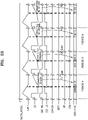
- FIG. 5B is a timing diagram according to an operation of the ZCD auto-calibration circuit 240 in the buck mode, according to another example embodiment of the inventive concepts.
- the bidirectional switching converter 110 may operate in the buck mode.
- An offset value may be represented as 5 bits.
- an initial offset value may be 10000.
- the ZCD auto-calibration circuit 240 may generate a check signal CHECK to monitor a change in a voltage of the switching node LX and whether the diode detector 243 detects a forward bias voltage. As illustrated in FIG. 5B , a point in time when the check signal CHECK is generated by turning off the second power MOSFET 220 may be earlier than a point in time when the switching current I_IND is zero. Because the switching current I_IND flows in a forward direction when the check signal CHECK is generated, the diode detector 243 may detect a forward bias voltage.
- the switching current I_IND may flow to a body diode of the second power MOSFET 220. Accordingly, the forward bias voltage may have a negative value.
- the forward bias voltage may be -0.7 V.
- the counter 244 may reduce an offset value in response to receiving a detection signal from the diode detector 243.
- the offset value may correspond to 01111 (i.e. 10000 reduced by 1). Because the offset value is reduced, a length of time during which the gate signal GD_LS of the second power MOSFET 220 maintains a logic high level may be longer than the first period PERIOD 1. A point in time when the second power MOSFET 220 is turned off during the second period PERIOD2 may be later than a point in time when the second power MOSFET 220 is turned off during the first period PERIOD 1. However, the point in time when the second power MOSFET 220 is turned off during the second period PERIOD2 may still be earlier than the point in time when the switching current I_IND is zero.
- the switching current I_IND may flow to the body diode of the second power MOSFET 220.
- the forward bias voltage may have a negative value.
- the forward bias voltage may be -0.4 V.
- the counter 244 may further reduce the offset value in response to receiving the detection signal from the diode detector 243.
- the offset value may correspond to 01110 (i.e. reduced by 2 with respect to the initial offset of 10000). Because the offset value is further reduced, the length of time during which the gate signal GD_LS of the second power MOSFET 220 maintains a logic high level during the sixth period PERIOD6 may be longer than the length of time of the fifth period PERIOD5. That is, the point in time when the second power MOSFET 220 is turned off during the sixth period PERIOD6 may be later than the point in time when the second power MOSFET 220 is turned off during a fifth period PERIOD5.
- the point in time when the second power MOSFET 220 is turned off during the sixth period PERIOD6 may be approximately same as the point in time when the switching current I_IND is zero. Accordingly, when the check signal CHECK is applied, the forward bias voltage may not be detected.
- the counter 244 may maintain the offset value in response to receiving a control signal, from the diode detector 243, indicating that the forward bias voltage is not detected.
- FIG. 6A is a timing diagram according to an operation of the ZCD auto-calibration circuit 240 in a boost mode, according to an example embodiment of the inventive concepts.
- the bidirectional switching converter 110 may operate in the boost mode.
- An offset value may be represented as 5 bits.
- an initial offset value may be "10000".
- the ZCD auto-calibration circuit 240 may generate a check signal CHECK to monitor a change in a voltage of the switching node LX and whether the diode detector 243 detects a forward bias voltage. As illustrated in FIG. 6A , a point in time when the check signal CHECK is generated by turning off the first power MOSFET 210 may be later than a point in time when the switching current I_IND is zero. When the check signal CHECK is generated, the switching current I_IND may flow in a forward direction.
- the diode detector 243 measuring both ends of the first power MOSFET 210 during the boost mode may not detect the forward bias voltage.
- the ZCD auto-calibration circuit 240 may check a differential value of a voltage of the switching node LX. Because the switching current I_IND flows in a forward direction, the voltage of the switching node LX may rapidly drop. As a magnitude of the forward switching current I_IND is reduced, a slope at which the voltage of the switching node LX drops may be reduced. The ZCD auto-calibration circuit 240 may detect that a differential value of the voltage of the switching node LX is greater than a threshold and increase an offset value by 1.
- the offset value may correspond to 10001 (10000 increased by 1). Because the offset value is increased, a length of time during which the gate signal GD_HS of the first power MOSFET 210 maintains a logic high level may be shorter than the first period PERIOD 1. A point in time when the first power MOSFET 210 is turned off during the second period PERIOD2 may be earlier than a point in time when the first power MOSFET 210 is turned off during the first period PERIOD 1. However, the point in time when the first power MOSFET 210 is turned off during the second period PERIOD2 may be later than the point in time when the switching current I_IND is zero.
- a maximum magnitude of the switching current I_IND flowing in the forward direction may also be reduced. Because the maximum magnitude of the switching current I_IND flowing in the forward direction is reduced, a slope at which the voltage of the switching node LX drops during the second period PERIOD2 may be less than a slope at which the voltage of the switching node LX drops during the first period PERIOD 1. However, the ZCD auto-calibration circuit 240 may detect that a differential value of the voltage of the switching node LX is greater than a threshold, even during the second period PERIOD2 and increase the offset value by one.
- the offset value may correspond to 10010 (increased by 2 with respect to an initial offset of 10000). Because the offset value is further increased, the length of time during which the gate signal GD_HS of the first power MOSFET 210 maintains a logic high level during the third period PERIOD3 may be shorter than the length of time of the second period PERIOD2. That is, the point in time when the first power MOSFET 210 is turned off during the third period PERIOD3 may be earlier than the point in time when the first power MOSFET 210 is turned off during the second period PERIOD2.
- the point in time when the first power MOSFET 210 is turned off during the third period PERIOD3 may be approximately same with the point in time when the switching current I_IND is zero. Because the length of time during which the first power MOSFET 210 maintains the logic high level is reduced, a maximum magnitude of the switching current I_IND flowing in the forward direction may also be further reduced. Because the maximum magnitude of the switching current I_IND flowing in the forward direction is reduced, a slope at which the voltage of the switching node LX drops during the third period PERIOD3 may be less than the slope at which the voltage of the switching node LX drops during the second period PERIOD2.
- the voltage of the switching node LX may be slowly reduced due to LC resonance caused by parasitic capacitances of the inductor and the switching node LX.
- the ZCD auto-calibration circuit 240 detects that the differential value of the voltage of the switching node LX is less than the threshold, and the offset value may be maintained at a value of 10010 without being increased.
- FIG. 6B is a timing diagram according to an operation of the ZCD auto-calibration circuit 240 in a boost mode according to another example embodiment of the inventive concepts.
- the bidirectional switching converter 110 may operate in the boost mode.
- An offset value may be represented as 5 bits.
- an initial offset value may be 10000.
- the ZCD auto-calibration circuit 240 may generate the check signal CHECK to monitor a change in a voltage of the switching node LX and whether the diode detector 243 detects a forward bias voltage. As illustrated in FIG. 6B , a point in time when the check signal CHECK is generated by turning off the first power MOSFET 220 may be earlier than a point in time when the switching current I_IND is zero. When the check signal CHECK is generated, the switching current I_IND may flow in a reverse direction.
- the diode detector 243 measuring voltages of both ends of the first power MOSFET 210 may detect a forward bias voltage.
- the switching current I_IND may flow to a body diode of the first power MOSFET 210.
- the forward bias voltage may have a positive value.
- the forward bias voltage may be +0.7 V.
- the counter 244 may reduce an offset value in response to receiving a detection signal from the diode detector 243.
- the offset value may correspond to 01111 (10000 reduced by 1). Because the offset value is reduced, a length of time during which the gate signal GD_HS of the first power MOSFET 210 maintains a logic high level may be longer than the first period PERIOD1. A point in time when the first power MOSFET 210 is turned off during the second period PERIOD2 may be later than a point in time when the first power MOSFET 210 is turned off during the first period PERIOD 1. However, the point in time when the first power MOSFET 210 is turned off during the second period PERIOD2 may still be earlier than the point in time when the switching current I_IND is zero.
- the switching current I_IND may flow to the body diode of the first power MOSFET 210.
- the forward bias voltage may have a positive value.
- the forward bias voltage may be +0.4 V.
- the counter 244 may further reduce the offset value in response to receiving the detection signal from the diode detector 243.
- the offset value may correspond to 01110 (reduced by 2 with respect to an initial offset of 10000). Because the offset value is further reduced, the length of time during which the gate signal GD_HS of the first power MOSFET 210 maintains a logic high level during the sixth period PERIOD6 may be longer than the length of time of the fifth period PERIOD5. The point in time when the first power MOSFET 210 is turned off during the sixth period PERIOD6 may be later than the point in time when the first power MOSFET 210 is turned off during the fifth period PERIOD5.
- the point in time when the first power MOSFET 210 is turned off during the sixth period PERIOD6 may be approximately same with the point in time when the switching current I_IND is zero. Accordingly, when the check signal CHECK is applied, the forward bias voltage may not be detected.
- the counter 244 may maintain the offset value in response to receiving a control signal, from the diode detector 243, indicating that the forward bias voltage is not detected.
- FIG. 7 illustrates Monte Carlo simulation results of detecting a zero current of a switching node according to an example embodiment of the inventive concepts.
- FIG. 7 illustrates Monte Carlo simulation results of 3000 samples for the switching current I_IND.
- the switching current I_IND may range from about -279 mA to about 216 mA.
- the switching current I_IND may range from about -44 mA to about 7.5 mA.
- the charger IC 100 including the ZCD auto-calibration circuit 240 performs switching at a point in time when the switching current I_IND is nearly zero, and thus, power consumption may be reduced and an efficient operation may be performed efficiently at low power.
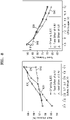
- FIG. 8 illustrates graphs showing efficiency improvement obtained by using a ZCD auto-calibration circuit according to an example embodiment of the inventive concepts.
- buck converter efficiency and boost converter efficiency are illustrated therein.
- a first graph 810 to a third graph 830 correspond to when the bidirectional switching converter 110 operates in a buck mode.
- the first graph 810 and the second graph 820 show the buck converter efficiency of the bidirectional switching converter 110 that does not include the ZCD auto-calibration circuit 240.
- the first graph 810 shows the buck converter efficiency based on an offset value for turning off the second power MOSFET 220 when a voltage of the battery 200 is about 3.4 V and when the switching current I_IND is zero.
- the first graph 810 shows high efficiency of about 86% to about 87% when the battery 200 is in a poor charging state (for example, about 3.4 V to about 3.6 V).
- the second graph 820 shows the buck converter efficiency based on the offset value for turning off the second power MOSFET 220 when the voltage of the battery 200 is about 4.1 V and when the switching current I_IND is zero.
- the second graph 820 shows high efficiency of about 89% when the battery 200 is in a good charging state (for example, about 4.0 V to about 4.1 V).
- a fourth graph 840 to a sixth graph 860 correspond to when the bidirectional switching converter 110 operates in the boost mode.
- the fourth graph 840 and the fifth graph 850 show the boost converter efficiency of the bidirectional switching converter 110 that does not include the ZCD auto-calibration circuit 240.
- the fourth graph 840 shows the boost converter efficiency based on an offset value for turning off the first power MOSFET 210 when an OTG voltage is about 4.8 V and when the switching current I_IND is zero.
- the fourth graph 840 shows high efficiency of about 90% when the OTG voltage is low.
- the fifth graph 850 shows the boost converter efficiency based on the offset value for turning off the first power MOSFET 210 when the OTG voltage is about 12 V and when the switching current I_IND is zero.
- the fifth graph 850 shows that the higher the OTG voltage, the higher the efficiency, and the lower the OTG voltage, the lower the efficiency. That is, it can be seen that, when the offset value is fixed and when the OTG voltage varies, the efficiency may be high in some of the OTG voltages, but the efficiency is low in the others of the OTG voltages.
- the sixth graph 860 shows the boost converter efficiency when the ZCD auto-calibration circuit 240 is provided to vary the offset value in real time. Referring to the sixth graph 860, it can be seen that the sixth graph 860 shows high efficiency for all OTG voltage values of the battery 200.
- FIG. 9 illustrates another example of the ZCD auto-calibration circuit 240 according to an example embodiment of the inventive concepts.
- the ZCD auto-calibration circuit 240 may include a first comparator 242-1 and a second comparator 242-2.
- the differentiator 241 may differentiate the voltage value of the switching node LX and transmit a differential value to the first comparator 242-1 and the second comparator 242-2.
- the first comparator 242-1 may compare a first threshold with the differential value. For example, when the differential value is greater than the first threshold, the first comparator 242-1 may output a control signal instructing to increase an offset to the counter 244.
- the second comparator 242-2 may compare a second threshold with the differential value. For example, when the differential value is greater than the second threshold, the second comparator 242-2 may output a control signal instructing to increase the offset to the counter 244. In this case, the second threshold may be greater than the first threshold.
- the counter 244 may receive control signals from the first comparator 242-1 and the second comparator 242-2. For example, when the differential value is greater than the first threshold and the second threshold, the counter 244 may increase the offset by 2. In another example, when the differential value is greater than the first threshold and less than the second threshold, the counter 244 may increase the offset by 1. In another example, when the differential value is less than the first threshold and the second threshold, the counter 244 may maintain the offset.
- the second period PERIOD2 of FIG. 5A may be omitted.
- the counter 244 may increase the offset value by 2, not by 1. Accordingly, a differential value measured during the next period of the first period PERIOD 1 may be changed to be close to a differential value of the third period PERIOD3.
- the electronic device 10 and/or the components included therein may include and/or be included in processing circuitry such as hardware including logic circuits; a hardware/software combination such as a processor executing software; or a combination thereof.
- processing circuitry such as hardware including logic circuits; a hardware/software combination such as a processor executing software; or a combination thereof.
- the processing circuity may include, but is not limited to, a central processing unit (CPU), a memory controller, an arithmetic logic unit (ALU), a digital signal processor, a microcomputer, a field programmable gate array (FPGA), and programmable logic unit, a microprocessor, application-specific integrated circuit (ASIC), etc.
- CPU central processing unit
- ALU arithmetic logic unit
- FPGA field programmable gate array
- ASIC application-specific integrated circuit
Landscapes
- Engineering & Computer Science (AREA)
- Power Engineering (AREA)
- Dc-Dc Converters (AREA)
Abstract
The inventive concepts provide a bidirectional switching converter including a first power metal oxide semiconductor field effect transistor (MOSFET) connecting an input voltage node to a switching node, a second power MOSFET connecting the switching node to a ground node, and a zero current detection (ZCD) auto-calibration circuit configured to perform one of an operation of generating a first offset for varying a turn-on time of the first power MOSFET according to an operation mode and an operation of generating a second offset for varying a turn-on time of the second power MOSFET according to the operation mode.
Description
- The inventive concepts relate to a converter, and more particularly, to a bidirectional switching converter and/or an operating method of the bidirectional switching converter.
- With the development of electronic technologies, various types of electronic devices have been used. Mobile electronic devices may be driven by battery devices included therein. According to an increase in power consumption of the electronic devices, battery capacity has been increased, and thus, batteries may be charged at various speeds according to magnitudes of voltages supplied by chargers, such as a fast charging method or a general charging method.
- The inventive concepts provide a bidirectional switching converter capable of tracking in real time a point in time when an inductor current is zero.
- According to an aspect of the inventive concepts, there is provided a bidirectional switching converter including a first power MOSFET connecting an input voltage node to a switching node, a second power MOSFET connecting the switching node to a ground node, and a zero current detection (ZCD) auto-calibration circuit configured to perform one of an operation of generating a first offset for varying a turn-on time of the first power MOSFET according to an operation mode and an operation of generating a second offset for varying a turn-on time of the second power MOSFET according to the operation mode, wherein the ZCD auto-calibration circuit may vary one of a value of the first offset and a value of the second offset, based on a differential value of a voltage of the switching node and a forward-bias detection result.
- According to another aspect of the inventive concepts, there is provided an electronic device including a battery, a bidirectional switching converter including a first power MOSFET connecting an input voltage node to a switching node, a second power MOSFET connecting the switching node to a ground node, and a zero current detection (ZCD) auto-calibration circuit configured to perform one of an operation of generating a first offset for varying a turn-on time of the first power MOSFET according to an operation mode and an operation of generating a second offset for varying a turn-on time of the second power MOSFET according to the operation mode, a first interface providing the battery with a power supplied from an external device, and a second interface providing the external device with a power output from the battery, wherein the ZCD auto-calibration circuit may change one of a value of the first offset and a value of the second offset, based on a differential value of a voltage of the switching node and a forward-bias detection result.
- According to another aspect of the inventive concepts, there is provided a method of operating a bidirectional switching converter including setting an initial offset, identifying an operation mode of the bidirectional switching converter, determining whether a forward bias voltage is detected between a first terminal and a second terminal of a first power MOSFET or between a first terminal and a second terminal of a second power MOSFET, according to the identified operation mode, and determining whether an absolute value of a differential value of a voltage of a switching node is greater than a threshold when the forward bias voltage is not detected, wherein the first power MOSFET may connect an input voltage node to the switching node, and the second power MOSFET may connect the switching node to a ground node.
- According to various embodiments, the turn-off time of one of the first power MOSFET and the second power MOSFET may be varied depending on a differential value of a voltage of the switching node and a forward-bias detection result. For instance, the turn-off time may be moved earlier in response to the differential value exceeding a first threshold. Equally, the turn-off time may be moved earlier in response to the forward bias voltage being detected.
- According to various embodiments, the turn-off time of one of the first power MOSFET and the second power MOSFET may be varied by changing a value of a respective (first or second) offset. Increasing an offset moves a turn-off time of the respective MOSFET earlier in time. Decreasing the offset moves the turn-off time of the respective MOSFET later in time.
- At least some of the above and other features of the invention are set out in the claims.
- Embodiments of the inventive concepts will be more clearly understood from the following detailed description taken in conjunction with the accompanying drawings in which:
-
FIG. 1 is a block diagram schematically illustrating an electronic device including a charger integrated circuit according to an example embodiment of the inventive concepts; -
FIG. 2 is a diagram of a bidirectional switching converter according to an example embodiment of the inventive concepts; -
FIG. 3A is a timing diagram illustrating when a point in time when a second power metal oxide semiconductor field effect transistor (MOSFET) is turned off is earlier than a point in time when a switching current is zero in a buck mode, according to an example embodiment of the inventive concepts; -
FIG. 3B is a timing diagram illustrating when the turn-off time of the second power MOSFET is later than the point in time when the switching current is zero in the buck mode, according to an example embodiment of the inventive concepts; -
FIG. 4 is a flowchart illustrating a method of operating a zero current detection (ZCD) auto-calibration circuit according to an example embodiment of the inventive concepts; -
FIG. 5A is a timing diagram illustrating an operation of the ZCD auto-calibration circuit in a buck mode, according to an example embodiment of the inventive concepts; -
FIG. 5B is a timing diagram illustrating an operation of the ZCD auto-calibration circuit in the buck mode, according to another example embodiment of the inventive concepts; -
FIG. 6A is a timing diagram illustrating an operation of a ZCD auto-calibration circuit in a boost mode, according to an example embodiment of the inventive concepts; -
FIG. 6B is a timing diagram illustrating another operation of the ZCD auto-calibration circuit in the boost mode, according to another example embodiment of the inventive concepts; -
FIG. 7 illustrates Monte Carlo simulation results of detecting a zero current of a switching node, according to an example embodiment of the inventive concepts; -
FIG. 8 illustrates graphs showing efficiency improvement obtained by using a ZCD auto-calibration circuit according to an example embodiment of the inventive concepts; and -
FIG. 9 illustrates another example of the ZCD auto-calibration circuit according to an example embodiment of the inventive concepts. - Hereinafter, embodiments of the inventive concepts will be described in detail with reference to the accompanying drawings.
-
FIG. 1 is a block diagram schematically illustrating an electronic device including a charger integrated circuit according to an example embodiment of the inventive concepts. - Referring to
FIG. 1 , anelectronic device 10 may include a charger integrated circuit (IC) 100 and abattery 200. In addition to this, theelectronic device 10 may further include a main processor and peripheral devices. For example, theelectronic device 10 may include a mobile device such as a smartphone, a tablet personal computer (PC), a cellular phone, a personal digital assistant (PDA), a laptop, a wearable device, a global positioning system (GPS) device, an e-book terminal, a digital broadcasting terminal, a motion picture experts group (MPEG) layer-3 (MP3) player, or a digital camera. For example, theelectronic device 10 may include an electric vehicle. - The
battery 200 may be mounted in theelectronic device 10. In one embodiment, thebattery 200 may be detachable from theelectronic device 10. Thebattery 200 may include one or a plurality of battery cells. The plurality of battery cells may be connected in series or in parallel to each other. When an external charging device is not connected to theelectronic device 10, thebattery 200 may supply power to theelectronic device 10. - The
charger IC 100 may charge thebattery 200 and may be referred to as a "battery charger". In addition, thecharger IC 100 may supply power to an external device (for example, a wired interface or a wireless interface) connected to thecharger IC 100 based on a voltage charged in thebattery 200. For example, the charger IC 100 may be implemented as an integrated circuit chip and may be mounted on a printed circuit board. - The charger IC 100 may include a
bidirectional switching converter 110 and acharging controller 120. Thebidirectional switching converter 110 may be implemented as a direct current (DC)-DC converter and may generate an output voltage by dropping or boosting an input voltage. When dropping the input voltage of thebidirectional switching converter 110, that is, during a buck conversion operation, a first power path may be formed in a first direction, and when boosting the input voltage, that is, during a boost conversion operation, a second power path may be formed in a second direction opposite to the first direction. - The
bidirectional switching converter 110 may operate in a buck mode (also referred to as buck single mode), a boost mode (or referred to as boost single mode), or a buck-boost mode (also referred to as buck-boost combined mode). - In the buck mode, the
bidirectional switching converter 110 may boost an input voltage by performing a buck conversion operation through a first switching operation and may charge thebattery 200 based on the boosted voltage. - In the boost mode, the
bidirectional switching converter 110 may drop a voltage input from thebattery 200 by performing a boost conversion operation through a second switching operation and may supply power to an external device based on the dropped voltage. - In the buck-boost mode, the
bidirectional switching converter 110 may perform the buck conversion operation or the boost conversion operation through a third switching operation according to a load current. In the buck-boost mode, thebidirectional switching converter 110 may charge thebattery 200 or supply power to an external device. - The
charging controller 120 may perform mode switching between a plurality of charging modes of thebidirectional switching converter 110, for example, a buck mode, a boost mode, and a buck-boost mode and may control a switching operation of thebidirectional switching converter 110 such that a voltage level of an output voltage is the same as or similar to a target voltage level in the plurality of charging modes. - The
charging controller 120 may receive a sensing current and a sensing voltage from thebidirectional switching converter 110 and may generate a control signal and a switching signal switching for controlling a switching operation in each charging mode of thebidirectional switching converter 110 based on the sensing current and the sensing voltage. - In some embodiments, the charger IC 100 may support at least one of various functions such as an under-voltage lockout (UVLO) function, an over-current protection (OCP) function, an over-voltage protection (OVP) function, a soft-start function of reducing an inrush current, a foldback current limit function, a Hiccup Mode function for short circuit protection, and an over-temperature protection (OTP) function so as to properly operate even under a power saving condition.
- In one embodiment, the
electronic device 10 may support wired charging and wireless charging and may include afirst power interface 310 and asecond power interface 320 for the wired charging and the wireless charging. In one embodiment, thefirst power interface 310 may be implemented as a wired power interface and may include a wired charging circuit. Thesecond power interface 320 may be implemented as a wireless power interface and may include a wireless charging circuit. - The
charger IC 100 may receive a first input voltage CHGIN from thefirst power interface 310 and/or a second input voltage WCIN from thesecond power interface 320 and may charge thebattery 200 based on the first input voltage CHGIN and/or the second input voltage WCIN in the buck mode. - The
charger IC 100 may provide power to thefirst power interface 310 and/or thesecond power interface 320 based on a voltage of thebattery 200 in the boost mode. - The
charger IC 100 may receive the first input voltage CHGIN from thefirst power interface 310 or the second input voltage WCIN from thesecond power interface 320, charge thebattery 200 based on the first input voltage CHGIN or the second input voltage WCIN, and provide power to thesecond power interface 320 or thefirst power interface 310 based on the first input voltage CHGIN or the second input voltage WCIN in the buck-boost mode. Alternatively, thecharger IC 100 may provide power to thesecond power interface 320 based on the first input voltage CHGIN and a voltage of thebattery 200 or may provide power to thefirst power interface 310 based on the second input voltage WCIN and the voltage of thebattery 200. - For example, a travel adapter (TA) or an auxiliary battery may be electrically connected to the
first power interface 310. The TA may convert alternate current (AC) voltages 110 V to 220 V, which are commercial voltages, or voltages supplied from another power supply (for example, a computer) into DC voltages required for charging thebattery 200 and provide the DC voltages to theelectronic device 10. Thecharger IC 100 may charge thebattery 200 or provide power to thesecond power interface 320 by using the first input voltage CHGIN received from the TA, the auxiliary battery, or so on in the buck mode. - For example, an on-the-go (OTG) device (for example, an OTG Universal Serial Bus (USB) device and so on) may be connected to the
first power interface 310, and the charger integratedcircuit 310 may provide power to the OTG device through thefirst power interface 310. In this case, thebidirectional switching converter 310 may provide power to the OTG device based on a voltage of thebattery 200 in the boost mode or may provide power to the OTG device in the buck mode while charging thebattery 200 based on the second input voltage WCIN from thesecond power interface 320. - As described above, the
electronic device 10 supports wired and wireless charging, and thecharger IC 100 has to operate in a plurality of charging modes including the buck mode, the boost mode, and the buck-boost mode to support wired charging and/or wireless charging, wired charging-wireless power supply, and wireless charging-wired power supply, and even when an input power supply is unstable, a seamless mode transition between the buck mode, the boost mode, and the buck-boost mode is required for stable wireless power supply or stable wired power supply. -
FIG. 2 is a diagram of abidirectional switching converter 110 according to an example embodiment of the inventive concepts. - Referring to
FIG. 2 , thebidirectional switching converter 110 may include a first power metal oxide semiconductor field effect transistor (MOSFET) 210, asecond power MOSFET 220, a pulse width modulation (PWM)controller 230, and a zero current detection (ZCD) auto-calibration circuit 240. - According to an embodiment, the
PWM controller 230 may output a first control signal PWM_HS and a second control signal PWM_LS. The first control signal PWM_HS may include a control signal for turning on/off thefirst power MOSFET 210. The second control signal PWM LS may include a control signal for turning on/off thesecond power MOSFET 220. ThePWM controller 230 may adjust an output ratio between the first control signal PWM_HS and the second control signal PWM_LS in response to a mode signal MODE instructing an operation mode. Thefirst power MOSFET 210 may be referred to as a high side (HS) switching device, and thesecond power MOSFET 220 may be referred to as a low side (LS) switching device. The first control signal PWM HS and the second control signal PWM_LS may be pulse width modulated signals. - The ZCD auto-
calibration circuit 240 may adjust in real time an offset value for detecting a zero current of a switching node LX. The ZCD auto-calibration circuit 240 may reduce or increase the offset value based on a differential value of the switching node LX and a detection result of adiode detector 243. - For example, while the
bidirectional switching converter 110 operates in the buck mode, thesecond power MOSFET 220 may be turned off before a switching current I_IND flowing through the switching node LX is zero. The ZCD auto-calibration circuit 240 may reduce the offset value to delay a point in time when thesecond power MOSFET 220 is turned off. - In another example, while the
bidirectional switching converter 110 operates in the buck mode, thesecond power MOSFET 220 may be turned off after the switching current I_IND flowing through the switching node LX is zero. The ZCD auto-calibration circuit 240 may increase the offset value to move up (e.g. move earlier) the point in time when thesecond power MOSFET 220 is turned off. Detailed operations of the ZCD auto-calibration circuit 240 are described below. - According to an embodiment, the ZCD auto-
calibration circuit 240 may further include adifferentiator 241, acomparator 242, and adiode detector 243. Thedifferentiator 241 may differentiate a voltage value of the switching node LX and output a result value to thecomparator 242. For example, the result value may be obtained by differentiating the voltage value of the switching node LX and taking an absolute value thereof. According to an embodiment, thedifferentiator 241 may include a capacitor for generating a differential current of the switching current I IND, a mirror circuit for copying the generated differential current, and a resistor for converting a copied differential current into a voltage in order to differentiate the voltage value of the switching node LX. - According to an embodiment, the
comparator 242 may receive a differential value from thedifferentiator 241 and compare the differential value with a threshold. When the result value is greater than the threshold, thecomparator 242 may output a control signal instructing to increase a count value (e.g. increase the offset) to thecounter 244. When the result value is less than the threshold, thecomparator 242 may output a control signal instructing to maintain the count value to thecounter 244. - According to an embodiment, the
diode detector 243 may detect a current direction of the switching current I_IND flowing through the switching node LX. In the buck mode, thediode detector 243 may compare a voltage of the switching node LX and a voltage of a ground node, which are both ends (i.e. a first terminal and a second terminal, respectively) of thesecond power MOSFET 220 in the buck mode, to detect whether a forward bias voltage is applied thereto. In the boost mode, thediode detector 243 may compare a voltage of the input voltage node VIN and a voltage of the switching node LX, which are both ends (i.e., a first terminal and a second terminal, respectively) of thefirst power MOSFET 210, to detect whether a forward bias voltage is applied thereto. Thediode detector 243 may generate a control signal for reducing an offset (e.g. decrease the counter) in response to detection of the forward bias voltage and transmit the control signal to thecounter 244. - According to an embodiment, the
counter 244 may adjust an offset value based on the control signal received from thedifferentiator 241 and thediode detector 243. For example, thecounter 244 may receive an up-control signal from thecomparator 242 while operating in the buck mode. The up-control signal received from thecomparator 242 may be a signal requesting to increase an offset value. Thecounter 244 may also receive a down-control signal from thediode detector 243. The down-control signal may be a signal requesting to increase an offset value. - According to an embodiment, the ZCD auto-
calibration circuit 240 may receive a mode signal MODE and output the adjusted offset value according to an operation mode. For example, when the ZCD auto-calibration circuit 240 receives the mode signal MODE indicating the buck mode, an offset value may be output to abuck comparator 250. In another example, when the ZCD auto-calibration circuit 240 receives the mode signal MODE indicating the boost mode, the offset value may be output to aboost comparator 260. A turn-on ratio or a turn-off ratio of thefirst power MOSFET 210 may vary according to the first control signal PWM_HS and a result of comparison performed by theboost comparator 260 based on the switching node LX and the offset value. A turn-on ratio or a turn-off ratio of thesecond power MOSFET 220 may vary according to the second control signal PWM_LS and a result of comparison performed by thebuck comparator 250 based on the switching node LX and the offset value. The turn-on ratios and turn-off ratios of thefirst power MOSFET 210 and thesecond power MOSFET 220 may vary, and thus, a turn-off time of thefirst power MOSFET 210 and a turn-off time of thesecond power MOSFET 220 may also vary. -
FIG. 3A is a timing diagram illustrating when a point in time when thesecond power MOSFET 220 is turned off is earlier than a point in time when the switching current I_IND is zero in the buck mode according to example embodiments of the inventive concepts. - Referring to
FIG. 3A , the switching current I_IND may flow in a forward direction. The forward direction may be a direction in which a current flows to thebattery 200. The switching current I_IND may have a positive value when the switching current I_IND flows in the forward direction. Thesecond power MOSFET 220 may be turned off when a gate signal GD_LS is transitioned to a logic low level. A check signal may be generated at a falling edge of the gate signal GD_LS. The check signal may be an impulse signal applied to a gate of thesecond power MOSFET 220. A voltage of the switching node LX may change according to a current direction of the switching current I IND at a point in time when the check signal is generated. Referring toFIG. 3A , the gate signal GD_LS of thesecond power MOSFET 220 may be transitioned to a logic low level at a point in time T1 to generate a check signal. The switching current I_IND may be zero at a point in time T2. That is, thesecond power MOSFET 220 may be first turned off before the switching current I IND is zero (T2 may be later than T1). In a case where the switching current I_IND flows in the forward direction when thesecond power MOSFET 220 is turned off, the switching current I IND may flow through a body diode of thesecond power MOSFET 220. When the switching current I_IND flows through the body diode of thesecond power MOSFET 220, a forward-bias diode drop may occur at the switching node LX. Due to the diode drop, a voltage of the switching node LX may drop by about 0.7 V. At a point in time T3, the ZCD auto-calibration circuit 240 may reduce an offset value to delay a point in time when the gate signal GD_LS of thesecond power MOSFET 220 is transitioned to a logic low level. -
FIG. 3B is a timing diagram illustrating when a point in time when thesecond power MOSFET 220 is turned off is later than a point in time when the switching current I IND is zero in the buck mode, according to an example embodiment of the inventive concepts. - Referring to
FIG. 3B , the switching current I IND may flow in a reverse direction. The reverse direction may be a direction in which a current flows from thebattery 200. The switching current I IND may have a negative value when flowing in the reverse direction. Referring toFIG. 3B , the switching current I_IND may be zero at a point in time T4. The gate signal GD_LS of thesecond power MOSFET 220 may be transitioned to a logic low level at a point in time T5 to generate a check signal. That is, thesecond power MOSFET 220 may be turned off after the switching current I_IND is zero (T5 may be later than T4). In a case where the switching current I IND flows in the reverse direction when thesecond power MOSFET 220 is turned off, a voltage of the switching node LX may rapidly increase. Because the voltage of the switching node LX rapidly increases, a differential value of the voltage of the switching node LX may be great enough to be greater than a threshold. When the differential value of the voltage of the switching node LX is greater than the threshold, the ZCD auto-calibration circuit 240 may increase an offset value to move up (e.g. bring forward) a point in time when the gate signal GD_LS of thesecond power MOSFET 220 is transitioned to a logic low level. -
FIG. 4 is a flowchart illustrating a method of operating the ZCD auto-calibration circuit according to an example embodiment of the inventive concepts. - Referring to
FIG. 4 , the ZCD auto-calibration circuit 240 may set an initial offset value duringoperation 410. The initial offset value may be a preset value during a manufacturing process. However, an environment of the manufacturing process and an operating environment may change depending on process, voltage, temperature (PVT) variation. Due to the PVT variation, a point in time when thesecond power MOSFET 220 is turned off according to the initial offset value may not be same with a point in time when the switching current I IND is zero. In addition, even when the PVT variation is removed, a point in time when thesecond power MOSFET 220 is turned off according to the initial offset value may not be same with a point in time when the switching current I IND is zero according to a voltage of thebattery 200 in a fully charged state and a voltage of thebattery 200 in a discharged state. - In
operation 420, the ZCD auto-calibration circuit 240 may determine whether an operation mode is a buck mode or a boost mode. For example, the ZCD auto-calibration circuit 240 may receive the mode signal MODE from the chargingcontroller 120. For example, when thebidirectional switching converter 110 supports the buck mode and the boost mode, the mode signal MODE may be 1 bit. The ZCD auto-calibration circuit 240 may identify that the boost mode is indicated when the mode signal MODE is in a logic high level and the buck mode is indicated when the mode signal MODE is in a logic low level. - In
operation 430, the ZCD auto-calibration circuit 240 may generate a check signal when thefirst power MOSFET 210 is turned off.Operation 430 may be implemented in response to the ZCD auto-calibration circuit 240 determining that the operation mode is the boost mode inoperation 420. The ZCD auto-calibration circuit 240 may monitor on/off of thefirst power MOSFET 210 based on the boost mode. The ZCD auto-calibration circuit 240 may generate a check signal when thefirst power MOSFET 210 is turned off. The check signal may include a control signal for activating thedifferentiator 241 to measure the differential value of the voltage of the switching node LX. - In
operation 435, the ZCD auto-calibration circuit 240 may determine whether a forward bias voltage is detected by thediode detector 243. When a point in time when thefirst power MOSFET 210 is turned off is earlier than a point in time when the switching current I_IND is zero, the switching current I_IND may flow to thediode detector 243. Thus, thediode detector 243 may detect a forward bias voltage. In this case, the forward bias voltage may be a positive voltage. When the forward bias voltage is detected, thecounter 244 may reduce an offset value. As the offset value is reduced, a time interval during which thefirst power MOSFET 210 is turned off may be reduced (e.g. the point in time at which thefirst power MOSFET 210 is first turned off may be delayed). This may reduce the time interval between the point in time point when the switching current I IND is zero and the point in time when thefirst power MOSFET 210 is turned off. As the time interval during which thefirst power MOSFET 210 is turned off is reduced, the forward bias voltage detected by thediode detector 243 may also be gradually reduced. When the forward bias voltage is not detected by thediode detector 243, the ZCD auto-calibration circuit 240 may proceed tooperation 440. - In
operation 440, the ZCD auto-calibration circuit 240 may determine whether the differential value of the voltage of the switching node LX is greater than a threshold. For example, the point in time when thefirst power MOSFET 210 is turned off may be later than the point in time when the switching current I_IND is zero. When thefirst power MOSFET 210 is turned off, the switching current I_IND may flow to thebattery 200. While the switching current I_IND flows into thebattery 200 to charge thebattery 200, a voltage of the switching node LX may be reduced. - Because the switching current I IND is a current flowing through an inductor, a magnitude of the switching current I IND flowing into the
battery 200 may depend on a magnitude of a slope at which the voltage of the switching node LX is reduced. That is, as the magnitude of the switching current I IND flowing into thebattery 200 increases, the voltage of the switching node LX may be rapidly reduced. When the magnitude of the switching current I IND flowing into thebattery 200 is increased, thecomparator 242 may determine that a differential value output from thedifferentiator 241 is greater than a threshold. In this case, the differential value may be a negative value. As an absolute value of the differential value is greater than the threshold, thecounter 244 may increase the offset value. When the offset value increases and the switching current I IND is 0 until thefirst power MOSFET 210 is turned off, the voltage of the switching node LX may be slowly reduced by LC resonance due to parasitic capacitances of the inductor and the switching node LX. Thecounter 244 may maintain the offset value when the voltage of the switching node LX is slowly reduced by the LC resonance and the absolute value of the differential value is less than the threshold. - In the embodiment described above, it is described that whether a forward bias voltage is detected is first determined by the
diode detector 243 inoperation 435, and then whether a differential value of a voltage of the switching node LX is greater than a threshold is determined by thedifferentiator 241 inoperation 440 but the inventive concepts are not limited thereto. According to various embodiments, the ZCD auto-calibration circuit 240 may also first determine whether a differential value is greater than a threshold inoperation 440 or may also simultaneously performoperation 435 andoperation 440. That is,operations - In
operation 450, the ZCD auto-calibration circuit 240 may generate a check signal when thesecond power MOSFET 220 is turned off.Operation 450 may be performed in response to the ZCD auto-calibration circuit 240 determining that the operation mode is the buck mode inoperation 420. The ZCD auto-calibration circuit 240 may monitor on/off of thesecond power MOSFET 220 based on the buck mode. The ZCD auto-calibration circuit 240 may generate a check signal when thesecond power MOSFET 220 is turned off. The check signal may be a control signal for activating thedifferentiator 241 to measure a differential value of a voltage of the switching node LX. - In operation 445, the ZCD auto-
calibration circuit 240 may determine whether a forward bias voltage is detected by thediode detector 243. When thesecond power MOSFET 220 is turned off before the switching current I_IND is zero, the switching current I_IND may flow to thediode detector 243. Thus,diode detector 243 may detect the forward bias voltage. In this case, the forward bias voltage may be a negative voltage. When the forward bias voltage is detected, thecounter 244 may reduce an offset value. As the offset value is reduced, a time interval during which thesecond power MOSFET 220 is turned off may be reduced (e.g. the point in time at which thesecond power MOSFET 220 is first turned off may be delayed). This may reduce a time interval between the point in time point when the switching current I_IND is zero and the point in time when thesecond power MOSFET 220 is turned off. As the time interval during which thesecond power MOSFET 220 is turned off is reduced, a magnitude of the forward bias voltage detected by thediode detector 243 may be gradually reduced. When the forward bias voltage is not detected by thediode detector 243, the ZCD auto-calibration circuit 240 may proceed tooperation 460. - In
operation 460, the ZCD auto-calibration circuit 240 may determine whether the differential value of the voltage of the switching node LX is greater than a threshold. For example, the point in time when thesecond power MOSFET 220 is turned off may be later than the point in time when the switching current I_IND is zero. When thesecond power MOSFET 220 is turned off, the switching current I_IND may be output from thebattery 200. While the switching current I IND is output from thebattery 200 to discharge thebattery 200, the voltage of the switching node LX may increase. - Because the switching current I IND is a current flowing through the inductor, a magnitude of the switching current I_IND output from the
battery 200 may depend on a magnitude of a slope at which the voltage of the switching node LX increases. That is, as the magnitude of the switching current I IND output from thebattery 200 increases, the voltage of the switching node LX may rapidly increase. When the magnitude of the switching current I_IND output from thebattery 200 is increased, thecomparator 242 may determine that a differential value output from thedifferentiator 241 is greater than a threshold. In this case, the differential value may be a positive value. As an absolute value of the differential value is greater than the threshold, thecounter 244 may increase the offset value. When the switching current I_IND is 0 and the offset value increases until thesecond power MOSFET 220 is turned off, the voltage of the switching node LX may be slowly reduced by LC resonance due to parasitic capacitances of the inductor and the switching node LX. Thecounter 244 may maintain the offset value when the voltage of the switching node LX is slowly reduced by the LC resonance and the absolute value of the differential value is less than the threshold. - In the embodiment described above, it is described that whether a forward bias voltage is detected is first determined by the
diode detector 243 inoperation 455, and then whether a differential value of a voltage of the switching node LX is greater than a threshold is determined by thedifferentiator 241 inoperation 460 but the inventive concepts are not limited thereto. According to various embodiments, the ZCD auto-calibration circuit 240 may also first determine whether a differential value is greater than a threshold inoperation 460 or may also simultaneously performoperation 455 andoperation 460. That is,operations -
FIG. 5A is a timing diagram according to an operation of the ZCD auto-calibration circuit 240 in a buck mode, according to an example embodiment of the inventive concepts. - Referring to
FIG. 5A , thebidirectional switching converter 110 may operate in the buck mode. An offset value may be represented as 5 bits. For example, an initial offset value may be "10000". - When the gate signal GD_LS of the
second power MOSFET 220 is transitioned to a logic low level in response to the buck mode, the ZCD auto-calibration circuit 240 may generate a check signal CHECK to monitor a change in a voltage of the switching node LX and whether thediode detector 243 detects a forward bias voltage. As illustrated inFIG. 5A , a point in time when the check signal CHECK is generated by turning off thesecond power MOSFET 220 may be later than a point in time when the switching current I_IND is zero. Because the switching current I_IND flows in a reverse direction when the check signal CHECK is generated, thediode detector 243 does not detect a forward bias voltage. The ZCD auto-calibration circuit 240 may check a differential value of the voltage of the switching node LX. Because the switching current I_IND flows in a reverse direction, the voltage of the switching node LX may be rapidly boosted. As a magnitude of the switching current I_IND in the reverse direction is reduced, a slope of the boosted voltage of the switching node LX may be reduced. The ZCD auto-calibration circuit 240 may detect that a differential value of the voltage of the switching node LX is greater than a threshold and generate a control signal UP that increases the offset value by 1, and the offset value may correspond to 10001 (i.e. 10000 increased by 1). - When a second period PERIOD2 starts, the offset value may correspond to 10001 (that is, 10000 increased by 1). Because the offset value is increased, a length of time during which the gate signal GD_LS of the
second power MOSFET 220 maintains a logic high level may be shorter than afirst period PERIOD 1. That is, a point in time when thesecond power MOSFET 220 is turned off during the second period PERIOD2 may be earlier than a point in time when thesecond power MOSFET 220 is turned off during thefirst period PERIOD 1. However, the point in time when thesecond power MOSFET 220 is turned off during the second period PERIOD2 may still be later than the point in time when the switching current I_IND is zero. Because the length of time during which thesecond power MOSFET 220 maintains the logic high level is reduced, a maximum magnitude of the switching current I_IND flowing in the reverse direction may also be reduced. Because the maximum magnitude of the switching current I_IND flowing in the reverse direction is reduced, a slope at which the voltage of the switching node LX is boosted during the second period PERIOD2 may be less than a slope at which the voltage of the switching node LX is boosted during thefirst period PERIOD 1. However, the ZCD auto-calibration circuit 240 may detect that a differential value of the voltage of the switching node LX is greater than a threshold, even during the second period PERIOD2 and generate the control signal UP for increasing the offset value by one. Following this, the offset value may correspond to 10010 (10001 increased by 1). - When a third period PERIOD3 starts, the offset value may correspond to 10010 (increased by 2 with respect to an initial offset of 10000). Because the offset value is further increased, the length of time during which the gate signal GD_LS of the
second power MOSFET 220 maintains a logic high level during the third period PERIOD3 may be shorter than the length of time of the second period PERIOD2. That is, the point in time when thesecond power MOSFET 220 is turned off during the third period PERIOD3 may be earlier than the point in time when thesecond power MOSFET 220 is turned off during the second period PERIOD2. For example, the point in time when thesecond power MOSFET 220 is turned off during the third period PERIOD3 may be approximately same with the point in time when the switching current I_IND is zero. Because the length of time during which thesecond power MOSFET 220 maintains the logic high level is reduced, a maximum magnitude of the switching current I_IND flowing in the reverse direction may also be further reduced. Because the maximum magnitude of the switching current I_IND flowing in the reverse direction is reduced, a slope at which the voltage of the switching node LX is boosted during the third period PERIOD3 may be less than the slope at which the voltage of the switching node LX is boosted during the second period PERIOD2. In addition, the voltage of the switching node LX may be slowly increased due to LC resonance caused by parasitic capacitances of the inductor and the switching node LX. The ZCD auto-calibration circuit 240 detects that the differential value of the voltage of the switching node LX is less than the threshold, and the offset value may be maintained at a value of 10010 without being increased. -
FIG. 5B is a timing diagram according to an operation of the ZCD auto-calibration circuit 240 in the buck mode, according to another example embodiment of the inventive concepts. - Referring to
FIG. 5B , thebidirectional switching converter 110 may operate in the buck mode. An offset value may be represented as 5 bits. For example, an initial offset value may be 10000. - When the gate signal GD_LS of the
second power MOSFET 220 is transitioned to a logic low level in response to the buck mode, the ZCD auto-calibration circuit 240 may generate a check signal CHECK to monitor a change in a voltage of the switching node LX and whether thediode detector 243 detects a forward bias voltage. As illustrated inFIG. 5B , a point in time when the check signal CHECK is generated by turning off thesecond power MOSFET 220 may be earlier than a point in time when the switching current I_IND is zero. Because the switching current I_IND flows in a forward direction when the check signal CHECK is generated, thediode detector 243 may detect a forward bias voltage. When the check signal CHECK is applied, the switching current I_IND may flow to a body diode of thesecond power MOSFET 220. Accordingly, the forward bias voltage may have a negative value. For example, the forward bias voltage may be -0.7 V. Thecounter 244 may reduce an offset value in response to receiving a detection signal from thediode detector 243. - When a fifth period PERIOD5 starts, the offset value may correspond to 01111 (i.e. 10000 reduced by 1). Because the offset value is reduced, a length of time during which the gate signal GD_LS of the
second power MOSFET 220 maintains a logic high level may be longer than thefirst period PERIOD 1. A point in time when thesecond power MOSFET 220 is turned off during the second period PERIOD2 may be later than a point in time when thesecond power MOSFET 220 is turned off during thefirst period PERIOD 1. However, the point in time when thesecond power MOSFET 220 is turned off during the second period PERIOD2 may still be earlier than the point in time when the switching current I_IND is zero. Accordingly, when the check signal CHECK is applied, the switching current I_IND may flow to the body diode of thesecond power MOSFET 220. The forward bias voltage may have a negative value. For example, the forward bias voltage may be -0.4 V. Thecounter 244 may further reduce the offset value in response to receiving the detection signal from thediode detector 243. - When a sixth period PERIOD6 starts, the offset value may correspond to 01110 (i.e. reduced by 2 with respect to the initial offset of 10000). Because the offset value is further reduced, the length of time during which the gate signal GD_LS of the
second power MOSFET 220 maintains a logic high level during the sixth period PERIOD6 may be longer than the length of time of the fifth period PERIOD5. That is, the point in time when thesecond power MOSFET 220 is turned off during the sixth period PERIOD6 may be later than the point in time when thesecond power MOSFET 220 is turned off during a fifth period PERIOD5. For example, the point in time when thesecond power MOSFET 220 is turned off during the sixth period PERIOD6 may be approximately same as the point in time when the switching current I_IND is zero. Accordingly, when the check signal CHECK is applied, the forward bias voltage may not be detected. Thecounter 244 may maintain the offset value in response to receiving a control signal, from thediode detector 243, indicating that the forward bias voltage is not detected. -
FIG. 6A is a timing diagram according to an operation of the ZCD auto-calibration circuit 240 in a boost mode, according to an example embodiment of the inventive concepts. - Referring to
FIG. 6A , thebidirectional switching converter 110 may operate in the boost mode. An offset value may be represented as 5 bits. For example, an initial offset value may be "10000". - When a gate signal GD_HS of the
first power MOSFET 210 is transitioned to a logic low level in response to the boost mode, the ZCD auto-calibration circuit 240 may generate a check signal CHECK to monitor a change in a voltage of the switching node LX and whether thediode detector 243 detects a forward bias voltage. As illustrated inFIG. 6A , a point in time when the check signal CHECK is generated by turning off thefirst power MOSFET 210 may be later than a point in time when the switching current I_IND is zero. When the check signal CHECK is generated, the switching current I_IND may flow in a forward direction. Thediode detector 243 measuring both ends of thefirst power MOSFET 210 during the boost mode may not detect the forward bias voltage. The ZCD auto-calibration circuit 240 may check a differential value of a voltage of the switching node LX. Because the switching current I_IND flows in a forward direction, the voltage of the switching node LX may rapidly drop. As a magnitude of the forward switching current I_IND is reduced, a slope at which the voltage of the switching node LX drops may be reduced. The ZCD auto-calibration circuit 240 may detect that a differential value of the voltage of the switching node LX is greater than a threshold and increase an offset value by 1. - When the second period PERIOD2 starts, the offset value may correspond to 10001 (10000 increased by 1). Because the offset value is increased, a length of time during which the gate signal GD_HS of the
first power MOSFET 210 maintains a logic high level may be shorter than thefirst period PERIOD 1. A point in time when thefirst power MOSFET 210 is turned off during the second period PERIOD2 may be earlier than a point in time when thefirst power MOSFET 210 is turned off during thefirst period PERIOD 1. However, the point in time when thefirst power MOSFET 210 is turned off during the second period PERIOD2 may be later than the point in time when the switching current I_IND is zero. Because the length of time during which thefirst power MOSFET 210 maintains the logic high level is reduced, a maximum magnitude of the switching current I_IND flowing in the forward direction may also be reduced. Because the maximum magnitude of the switching current I_IND flowing in the forward direction is reduced, a slope at which the voltage of the switching node LX drops during the second period PERIOD2 may be less than a slope at which the voltage of the switching node LX drops during thefirst period PERIOD 1. However, the ZCD auto-calibration circuit 240 may detect that a differential value of the voltage of the switching node LX is greater than a threshold, even during the second period PERIOD2 and increase the offset value by one. - When the third period PERIOD3 starts, the offset value may correspond to 10010 (increased by 2 with respect to an initial offset of 10000). Because the offset value is further increased, the length of time during which the gate signal GD_HS of the
first power MOSFET 210 maintains a logic high level during the third period PERIOD3 may be shorter than the length of time of the second period PERIOD2. That is, the point in time when thefirst power MOSFET 210 is turned off during the third period PERIOD3 may be earlier than the point in time when thefirst power MOSFET 210 is turned off during the second period PERIOD2. For example, the point in time when thefirst power MOSFET 210 is turned off during the third period PERIOD3 may be approximately same with the point in time when the switching current I_IND is zero. Because the length of time during which thefirst power MOSFET 210 maintains the logic high level is reduced, a maximum magnitude of the switching current I_IND flowing in the forward direction may also be further reduced. Because the maximum magnitude of the switching current I_IND flowing in the forward direction is reduced, a slope at which the voltage of the switching node LX drops during the third period PERIOD3 may be less than the slope at which the voltage of the switching node LX drops during the second period PERIOD2. In addition, the voltage of the switching node LX may be slowly reduced due to LC resonance caused by parasitic capacitances of the inductor and the switching node LX. The ZCD auto-calibration circuit 240 detects that the differential value of the voltage of the switching node LX is less than the threshold, and the offset value may be maintained at a value of 10010 without being increased. -
FIG. 6B is a timing diagram according to an operation of the ZCD auto-calibration circuit 240 in a boost mode according to another example embodiment of the inventive concepts. - Referring to
FIG. 6B , thebidirectional switching converter 110 may operate in the boost mode. An offset value may be represented as 5 bits. For example, an initial offset value may be 10000. - When the gate signal GD_LS of the
first power MOSFET 210 is transitioned to a logic low level in response to the boost mode, the ZCD auto-calibration circuit 240 may generate the check signal CHECK to monitor a change in a voltage of the switching node LX and whether thediode detector 243 detects a forward bias voltage. As illustrated inFIG. 6B , a point in time when the check signal CHECK is generated by turning off thefirst power MOSFET 220 may be earlier than a point in time when the switching current I_IND is zero. When the check signal CHECK is generated, the switching current I_IND may flow in a reverse direction. During the boost mode, thediode detector 243 measuring voltages of both ends of thefirst power MOSFET 210 may detect a forward bias voltage. When the check signal CHECK is applied, the switching current I_IND may flow to a body diode of thefirst power MOSFET 210. Accordingly, the forward bias voltage may have a positive value. For example, the forward bias voltage may be +0.7 V. Thecounter 244 may reduce an offset value in response to receiving a detection signal from thediode detector 243. - When the fifth period PERIOD5 starts, the offset value may correspond to 01111 (10000 reduced by 1). Because the offset value is reduced, a length of time during which the gate signal GD_HS of the
first power MOSFET 210 maintains a logic high level may be longer than the first period PERIOD1. A point in time when thefirst power MOSFET 210 is turned off during the second period PERIOD2 may be later than a point in time when thefirst power MOSFET 210 is turned off during thefirst period PERIOD 1. However, the point in time when thefirst power MOSFET 210 is turned off during the second period PERIOD2 may still be earlier than the point in time when the switching current I_IND is zero. Accordingly, when the check signal CHECK is applied, the switching current I_IND may flow to the body diode of thefirst power MOSFET 210. The forward bias voltage may have a positive value. For example, the forward bias voltage may be +0.4 V. Thecounter 244 may further reduce the offset value in response to receiving the detection signal from thediode detector 243. - When the sixth period PERIOD6 starts, the offset value may correspond to 01110 (reduced by 2 with respect to an initial offset of 10000). Because the offset value is further reduced, the length of time during which the gate signal GD_HS of the
first power MOSFET 210 maintains a logic high level during the sixth period PERIOD6 may be longer than the length of time of the fifth period PERIOD5. The point in time when thefirst power MOSFET 210 is turned off during the sixth period PERIOD6 may be later than the point in time when thefirst power MOSFET 210 is turned off during the fifth period PERIOD5. For example, the point in time when thefirst power MOSFET 210 is turned off during the sixth period PERIOD6 may be approximately same with the point in time when the switching current I_IND is zero. Accordingly, when the check signal CHECK is applied, the forward bias voltage may not be detected. Thecounter 244 may maintain the offset value in response to receiving a control signal, from thediode detector 243, indicating that the forward bias voltage is not detected. -
FIG. 7 illustrates Monte Carlo simulation results of detecting a zero current of a switching node according to an example embodiment of the inventive concepts. -
FIG. 7 illustrates Monte Carlo simulation results of 3000 samples for the switching current I_IND. - According to an embodiment, when the ZCD auto-
calibration circuit 240 is deactivated, and when thefirst power MOSFET 210 or thesecond power MOSFET 220 is turned off, the switching current I_IND may range from about -279 mA to about 216 mA. - According to an embodiment, when the ZCD auto-
calibration circuit 240 is activated, and when thefirst power MOSFET 210 or thesecond power MOSFET 220 is turned off, the switching current I_IND may range from about -44 mA to about 7.5 mA. - According to the embodiments described above, the
charger IC 100 including the ZCD auto-calibration circuit 240 according to the inventive concepts performs switching at a point in time when the switching current I_IND is nearly zero, and thus, power consumption may be reduced and an efficient operation may be performed efficiently at low power. -
FIG. 8 illustrates graphs showing efficiency improvement obtained by using a ZCD auto-calibration circuit according to an example embodiment of the inventive concepts. - Referring to
FIG. 8 , buck converter efficiency and boost converter efficiency are illustrated therein. According to an embodiment, afirst graph 810 to athird graph 830 correspond to when thebidirectional switching converter 110 operates in a buck mode. Thefirst graph 810 and thesecond graph 820 show the buck converter efficiency of thebidirectional switching converter 110 that does not include the ZCD auto-calibration circuit 240. - The
first graph 810 shows the buck converter efficiency based on an offset value for turning off thesecond power MOSFET 220 when a voltage of thebattery 200 is about 3.4 V and when the switching current I_IND is zero. Thefirst graph 810 shows high efficiency of about 86% to about 87% when thebattery 200 is in a poor charging state (for example, about 3.4 V to about 3.6 V). - The
second graph 820 shows the buck converter efficiency based on the offset value for turning off thesecond power MOSFET 220 when the voltage of thebattery 200 is about 4.1 V and when the switching current I_IND is zero. Thesecond graph 820 shows high efficiency of about 89% when thebattery 200 is in a good charging state (for example, about 4.0 V to about 4.1 V). - That is, it can be seen that, when the offset value is fixed and when the voltage of the
battery 200 varies, the efficiency may be high in some voltages of thebattery 200, but the efficiency may be low in the other voltages. This is because it does not guarantee that thesecond power MOSFET 220 is turned off when the switching current I_IND is zero in the other voltages. - The
third graph 830 shows the buck converter efficiency when the ZCD auto-calibration circuit 240 is provided to vary the offset value in real time. Referring to thethird graph 830, it can be seen that the efficiency is high whether thebattery 200 is in a good charging state or a bad charging state. For example, when thebattery 200 is in a poor charging state, the efficiency is equal to efficiency shown in thefirst graph 810, and when thebattery 200 is in a good charging state, the efficiency is equal to efficiency shown in thesecond graph 820. - According to another embodiment, a
fourth graph 840 to asixth graph 860 correspond to when thebidirectional switching converter 110 operates in the boost mode. Thefourth graph 840 and thefifth graph 850 show the boost converter efficiency of thebidirectional switching converter 110 that does not include the ZCD auto-calibration circuit 240. - The
fourth graph 840 shows the boost converter efficiency based on an offset value for turning off thefirst power MOSFET 210 when an OTG voltage is about 4.8 V and when the switching current I_IND is zero. Thefourth graph 840 shows high efficiency of about 90% when the OTG voltage is low. - The
fifth graph 850 shows the boost converter efficiency based on the offset value for turning off thefirst power MOSFET 210 when the OTG voltage is about 12 V and when the switching current I_IND is zero. Thefifth graph 850 shows that the higher the OTG voltage, the higher the efficiency, and the lower the OTG voltage, the lower the efficiency. That is, it can be seen that, when the offset value is fixed and when the OTG voltage varies, the efficiency may be high in some of the OTG voltages, but the efficiency is low in the others of the OTG voltages. - The
sixth graph 860 shows the boost converter efficiency when the ZCD auto-calibration circuit 240 is provided to vary the offset value in real time. Referring to thesixth graph 860, it can be seen that thesixth graph 860 shows high efficiency for all OTG voltage values of thebattery 200. -
FIG. 9 illustrates another example of the ZCD auto-calibration circuit 240 according to an example embodiment of the inventive concepts. - Referring to
FIG. 9 , the ZCD auto-calibration circuit 240 may include a first comparator 242-1 and a second comparator 242-2. Thedifferentiator 241 may differentiate the voltage value of the switching node LX and transmit a differential value to the first comparator 242-1 and the second comparator 242-2. - The first comparator 242-1 may compare a first threshold with the differential value. For example, when the differential value is greater than the first threshold, the first comparator 242-1 may output a control signal instructing to increase an offset to the
counter 244. - The second comparator 242-2 may compare a second threshold with the differential value. For example, when the differential value is greater than the second threshold, the second comparator 242-2 may output a control signal instructing to increase the offset to the
counter 244. In this case, the second threshold may be greater than the first threshold. - The
counter 244 may receive control signals from the first comparator 242-1 and the second comparator 242-2. For example, when the differential value is greater than the first threshold and the second threshold, thecounter 244 may increase the offset by 2. In another example, when the differential value is greater than the first threshold and less than the second threshold, thecounter 244 may increase the offset by 1. In another example, when the differential value is less than the first threshold and the second threshold, thecounter 244 may maintain the offset. - When the ZCD auto-
calibration circuit 240 illustrated inFIG. 9 is used, the second period PERIOD2 ofFIG. 5A may be omitted. For example, when the differential value measured during thefirst period PERIOD 1 is greater than the first threshold and the second threshold, thecounter 244 may increase the offset value by 2, not by 1. Accordingly, a differential value measured during the next period of thefirst period PERIOD 1 may be changed to be close to a differential value of the third period PERIOD3. - According to the embodiments described above, a magnitude of the offset may be varied by comparing the differential value of the switching node LX with a plurality of threshold values, but the inventive concepts are not limited thereto. In various embodiments, the
diode detector 243 may set various magnitudes for reducing an offset by comparing a magnitude of a forward bias voltage with a plurality of thresholds without comparing the magnitude of the forward bias voltage with a single threshold. - Additionally, the
electronic device 10 and/or the components included therein may include and/or be included in processing circuitry such as hardware including logic circuits; a hardware/software combination such as a processor executing software; or a combination thereof. For example, the processing circuity may include, but is not limited to, a central processing unit (CPU), a memory controller, an arithmetic logic unit (ALU), a digital signal processor, a microcomputer, a field programmable gate array (FPGA), and programmable logic unit, a microprocessor, application-specific integrated circuit (ASIC), etc. - While the inventive concepts have been particularly shown and described with reference to embodiments thereof, it will be understood that various changes in form and details may be made therein without departing from the scope of the following claims.
Claims (12)
- A bidirectional switching converter comprising:a first power metal oxide semiconductor field effect transistor, hereinafter referred to as MOSFET, connecting an input voltage node to a switching node;a second power MOSFET connecting the switching node to a ground node; anda zero current detection, hereinafter referred to as ZCD, auto-calibration circuit configured to perform one of an operation of generating a first offset for varying a turn-off time of the first power MOSFET according to an operation mode and an operation of generating a second offset for varying a turn-off time of the second power MOSFET according to the operation mode,wherein the ZCD auto-calibration circuit is configured to change one of a value of the first offset and a value of the second offset, based on a differential value of a voltage of the switching node and a forward-bias detection result.
- The bidirectional switching converter of claim 1, wherein the ZCD auto-calibration circuit further comprises:a differentiator configured to differentiate the voltage of the switching node to obtain the differential value;a comparator configured to receive the differential value from the differentiator, compare the differential value with a first threshold and output an offset increase signal for increasing one of the first offset and the second offset;a diode detector configured to detect one of a forward bias voltage between a first terminal and a second terminal of the first power MOSFET and a forward bias voltage between a first terminal and a second terminal of the second power MOSFET according to the operation mode, and output an offset decrease signal for reducing one of the first offset and the second offset according to a result of the detection; anda counter configured to receive the offset increase signal and the offset decrease signal and vary one of the first offset and the second offset.
- The bidirectional switching converter of claim 2, wherein the comparator is further configured to generate the offset increase signal to the counter when the differential value is greater than the first threshold.
- The bidirectional switching converter of claim 2 or claim 3, wherein the diode detector is further configured to detect the forward bias voltage between the first terminal and the second terminal of the second power MOSFET when the operation mode corresponds to a buck mode, and
detect the forward bias voltage between the first terminal and the second terminal of the first power MOSFET when the operation mode corresponds to a boost mode. - The bidirectional switching converter of claim 4, wherein the second power MOSFET is configured to have a turn-off time moved earlier in response to the offset increase signal when the operation mode is the buck mode and the offset increase signal is input to the counter.
- The bidirectional switching converter of claim 4 or claim 5, wherein the second power MOSFET is configured to have a turn-off time delayed in response to the offset decrease signal when the operation mode is the buck mode and the offset decrease signal is input to the counter.
- The bidirectional switching converter of any of claims 4-6, wherein the first power MOSFET is configured to have a turn-off time delayed in response to the offset decrease signal when the operation mode is the boost mode and the offset decrease signal is input to the counter.
- The bidirectional switching converter of any of claims 4-7, wherein the first power MOSFET is configured to have a turn-off time moved earlier in response to the offset increase signal when the operation mode is the boost mode and the offset increase signal is input to the counter.
- The bidirectional switching converter of any of claims 2-8, wherein the ZCD auto-calibration circuit further comprises an additional comparator receiving the differential value from the differentiator and comparing the differential value with a second threshold, and
wherein the counter is further configured to increase an increment of offset to be greater when the differential value is greater than the first threshold and the second threshold. - A method of operating a bidirectional switching converter, the method comprising:setting an initial offset;identifying an operation mode of the bidirectional switching converter;determining whether a forward bias voltage is detected between a first terminal and a second terminal of a first power metal oxide semiconductor field effect transistor, hereinafter referred to as MOSFET, or between a first terminal and a second terminal of a second power MOSFET, according to the identified operation mode; anddetermining whether an absolute value of a differential value of a voltage of a switching node is greater than a threshold when the forward bias voltage is not detected,wherein the first power MOSFET connects an input voltage node to the switching node, andwherein the second power MOSFET connects the switching node to a ground node.
- The method of claim 10, wherein, when the identified operation mode corresponds to a buck mode,the determining of whether the forward bias voltage is detected comprises:detecting the forward bias voltage between the first terminal and the second terminal of the second power MOSFET; andreducing the initial offset when the forward bias voltage is detected, andwherein the method further comprises increasing the initial offset when the absolute value of the differential voltage is greater than the threshold.
- The method of claim 10 or claim 11, wherein, when the identified operation mode corresponds to a boost mode, the determining of whether the forward bias voltage is detected comprises:detecting the forward bias voltage between the first terminal and the second terminal of the first power MOSFET; anddecreasing the initial offset when the forward bias voltage is detected, andwherein the method further comprises increasing the initial offset when the absolute value is greater than the threshold.
Applications Claiming Priority (2)
| Application Number | Priority Date | Filing Date | Title |
|---|---|---|---|
| KR20210017870 | 2021-02-08 | ||
| KR1020210141981A KR20220114463A (en) | 2021-02-08 | 2021-10-22 | Bidirectional switching convereter and operating method thereof |
Publications (1)
| Publication Number | Publication Date |
|---|---|
| EP4040663A1 true EP4040663A1 (en) | 2022-08-10 |
Family
ID=80447420
Family Applications (1)
| Application Number | Title | Priority Date | Filing Date |
|---|---|---|---|
| EP22155678.0A Pending EP4040663A1 (en) | 2021-02-08 | 2022-02-08 | Bidirectional switching converter and operating method thereof |
Country Status (3)
| Country | Link |
|---|---|
| US (1) | US20220255435A1 (en) |
| EP (1) | EP4040663A1 (en) |
| CN (1) | CN114915169A (en) |
Families Citing this family (1)
| Publication number | Priority date | Publication date | Assignee | Title |
|---|---|---|---|---|
| CN115956919B (en) * | 2022-12-07 | 2023-11-17 | 上海类比半导体技术有限公司 | Offset self-calibration circuit, method, chip and system |
-
2022
- 2022-02-07 US US17/665,933 patent/US20220255435A1/en active Pending
- 2022-02-08 EP EP22155678.0A patent/EP4040663A1/en active Pending
- 2022-02-08 CN CN202210117545.5A patent/CN114915169A/en active Pending
Non-Patent Citations (1)
| Title |
|---|
| SUN ZHUOCHAO ET AL: "Adaptive Gate Switching Control for Discontinuous Conduction Mode DC-DC Conve", IEEE TRANSACTIONS ON POWER ELECTRONICS, INSTITUTE OF ELECTRICAL AND ELECTRONICS ENGINEERS, USA, vol. 29, no. 3, 1 March 2014 (2014-03-01), pages 1311 - 1320, XP011527635, ISSN: 0885-8993, [retrieved on 20130919], DOI: 10.1109/TPEL.2013.2263579 * |
Also Published As
| Publication number | Publication date |
|---|---|
| CN114915169A (en) | 2022-08-16 |
| US20220255435A1 (en) | 2022-08-11 |
Similar Documents
| Publication | Publication Date | Title |
|---|---|---|
| US8564273B2 (en) | Analog current limit adjustment for linear and switching regulators | |
| US9430008B2 (en) | Apparatus and method for optimizing use of NVDC chargers | |
| US9218043B2 (en) | Battery charge system and method capable of operating in different configurations | |
| US9479060B2 (en) | Control circuit, battery power supply device and control method | |
| US9246348B2 (en) | Battery charge modulator with boost capability | |
| US8362748B2 (en) | Voltage comparison circuit | |
| US7592777B2 (en) | Current mode battery charger controller | |
| US9368992B2 (en) | Power storage system and secondary battery control method | |
| US6906497B2 (en) | Enabling circuit for avoiding negative voltage transients | |
| US10079498B2 (en) | Charging circuit, power management circuit, and electronic device using the same | |
| CN105762892A (en) | Step-down output and charging and discharging protection system for lithium battery | |
| US20200076305A1 (en) | Electronic converter and method of operating an electronic converter | |
| US6949912B2 (en) | Enabling circuit for avoiding negative voltage transients | |
| EP4040663A1 (en) | Bidirectional switching converter and operating method thereof | |
| US10644595B2 (en) | Power converter controller | |
| EP2583376B1 (en) | Switching regulator with input current limiting capabilities | |
| US20240055992A1 (en) | Three-level buck converter configurable for two-level buck converter mode operation | |
| US20240030822A1 (en) | Dc-to-dc converter and integrated circuit including the same | |
| US20220294236A1 (en) | Battery system and operating method of electronic device including the same | |
| KR20220127722A (en) | Battery system and operating method of electronic device including the smae | |
| KR20220114463A (en) | Bidirectional switching convereter and operating method thereof | |
| US20200136495A1 (en) | Power control circuit and a power control method | |
| WO2020242786A1 (en) | Techniques for controlling a single-inductor multiple-output (simo) switched-mode power supply (smps) | |
| US20230155507A1 (en) | Charger integrated circuit including bidirectional switching converter, and electronic device including the charger integrated circuit | |
| US20230059963A1 (en) | Buck converter including a bootstrap capacitor and an operating method thereof |
Legal Events
| Date | Code | Title | Description |
|---|---|---|---|
| PUAI | Public reference made under article 153(3) epc to a published international application that has entered the european phase |
Free format text: ORIGINAL CODE: 0009012 |
|
| STAA | Information on the status of an ep patent application or granted ep patent |
Free format text: STATUS: REQUEST FOR EXAMINATION WAS MADE |
|
| 17P | Request for examination filed |
Effective date: 20220208 |
|
| AK | Designated contracting states |
Kind code of ref document: A1 Designated state(s): AL AT BE BG CH CY CZ DE DK EE ES FI FR GB GR HR HU IE IS IT LI LT LU LV MC MK MT NL NO PL PT RO RS SE SI SK SM TR |
|
| P01 | Opt-out of the competence of the unified patent court (upc) registered |
Effective date: 20230519 |
|
| STAA | Information on the status of an ep patent application or granted ep patent |
Free format text: STATUS: EXAMINATION IS IN PROGRESS |
|
| 17Q | First examination report despatched |
Effective date: 20231116 |