EP3979483A1 - Transformer arrangement and method for voltage conversion - Google Patents
Transformer arrangement and method for voltage conversion Download PDFInfo
- Publication number
- EP3979483A1 EP3979483A1 EP20200063.4A EP20200063A EP3979483A1 EP 3979483 A1 EP3979483 A1 EP 3979483A1 EP 20200063 A EP20200063 A EP 20200063A EP 3979483 A1 EP3979483 A1 EP 3979483A1
- Authority
- EP
- European Patent Office
- Prior art keywords
- tap
- transformer
- arm
- arrangement
- voltage
- Prior art date
- Legal status (The legal status is an assumption and is not a legal conclusion. Google has not performed a legal analysis and makes no representation as to the accuracy of the status listed.)
- Pending
Links
- 238000006243 chemical reaction Methods 0.000 title claims description 15
- 238000000034 method Methods 0.000 title claims description 11
- 238000004804 winding Methods 0.000 claims abstract description 52
- 230000008878 coupling Effects 0.000 claims abstract description 9
- 238000010168 coupling process Methods 0.000 claims abstract description 9
- 238000005859 coupling reaction Methods 0.000 claims abstract description 9
- 239000004065 semiconductor Substances 0.000 claims description 22
- 238000001914 filtration Methods 0.000 claims description 6
- 230000005669 field effect Effects 0.000 claims description 4
- 238000011161 development Methods 0.000 description 33
- 230000018109 developmental process Effects 0.000 description 33
- 239000003990 capacitor Substances 0.000 description 22
- 239000011159 matrix material Substances 0.000 description 20
- 238000013461 design Methods 0.000 description 14
- 230000007935 neutral effect Effects 0.000 description 12
- 230000001939 inductive effect Effects 0.000 description 6
- 238000001816 cooling Methods 0.000 description 4
- 238000004519 manufacturing process Methods 0.000 description 4
- 230000004913 activation Effects 0.000 description 3
- 238000013016 damping Methods 0.000 description 3
- 238000007667 floating Methods 0.000 description 3
- 239000000463 material Substances 0.000 description 3
- 230000000116 mitigating effect Effects 0.000 description 3
- 201000010273 Porphyria Cutanea Tarda Diseases 0.000 description 2
- 230000002457 bidirectional effect Effects 0.000 description 2
- 230000001276 controlling effect Effects 0.000 description 2
- 238000012423 maintenance Methods 0.000 description 2
- NUSQOFAKCBLANB-UHFFFAOYSA-N phthalocyanine tetrasulfonic acid Chemical compound C12=CC(S(=O)(=O)O)=CC=C2C(N=C2NC(C3=CC=C(C=C32)S(O)(=O)=O)=N2)=NC1=NC([C]1C=CC(=CC1=1)S(O)(=O)=O)=NC=1N=C1[C]3C=CC(S(O)(=O)=O)=CC3=C2N1 NUSQOFAKCBLANB-UHFFFAOYSA-N 0.000 description 2
- 230000008859 change Effects 0.000 description 1
- 238000011217 control strategy Methods 0.000 description 1
- 230000001419 dependent effect Effects 0.000 description 1
- 238000011982 device technology Methods 0.000 description 1
- 238000007599 discharging Methods 0.000 description 1
- 230000000694 effects Effects 0.000 description 1
- 238000005516 engineering process Methods 0.000 description 1
- 238000009499 grossing Methods 0.000 description 1
- 239000007788 liquid Substances 0.000 description 1
- 230000010355 oscillation Effects 0.000 description 1
- 230000001105 regulatory effect Effects 0.000 description 1
- 230000004044 response Effects 0.000 description 1
Images


Classifications
-
- H—ELECTRICITY
- H02—GENERATION; CONVERSION OR DISTRIBUTION OF ELECTRIC POWER
- H02M—APPARATUS FOR CONVERSION BETWEEN AC AND AC, BETWEEN AC AND DC, OR BETWEEN DC AND DC, AND FOR USE WITH MAINS OR SIMILAR POWER SUPPLY SYSTEMS; CONVERSION OF DC OR AC INPUT POWER INTO SURGE OUTPUT POWER; CONTROL OR REGULATION THEREOF
- H02M5/00—Conversion of ac power input into ac power output, e.g. for change of voltage, for change of frequency, for change of number of phases
- H02M5/02—Conversion of ac power input into ac power output, e.g. for change of voltage, for change of frequency, for change of number of phases without intermediate conversion into dc
- H02M5/04—Conversion of ac power input into ac power output, e.g. for change of voltage, for change of frequency, for change of number of phases without intermediate conversion into dc by static converters
- H02M5/10—Conversion of ac power input into ac power output, e.g. for change of voltage, for change of frequency, for change of number of phases without intermediate conversion into dc by static converters using transformers
- H02M5/12—Conversion of ac power input into ac power output, e.g. for change of voltage, for change of frequency, for change of number of phases without intermediate conversion into dc by static converters using transformers for conversion of voltage or current amplitude only
-
- H—ELECTRICITY
- H02—GENERATION; CONVERSION OR DISTRIBUTION OF ELECTRIC POWER
- H02M—APPARATUS FOR CONVERSION BETWEEN AC AND AC, BETWEEN AC AND DC, OR BETWEEN DC AND DC, AND FOR USE WITH MAINS OR SIMILAR POWER SUPPLY SYSTEMS; CONVERSION OF DC OR AC INPUT POWER INTO SURGE OUTPUT POWER; CONTROL OR REGULATION THEREOF
- H02M1/00—Details of apparatus for conversion
- H02M1/0095—Hybrid converter topologies, e.g. NPC mixed with flying capacitor, thyristor converter mixed with MMC or charge pump mixed with buck
-
- H—ELECTRICITY
- H02—GENERATION; CONVERSION OR DISTRIBUTION OF ELECTRIC POWER
- H02M—APPARATUS FOR CONVERSION BETWEEN AC AND AC, BETWEEN AC AND DC, OR BETWEEN DC AND DC, AND FOR USE WITH MAINS OR SIMILAR POWER SUPPLY SYSTEMS; CONVERSION OF DC OR AC INPUT POWER INTO SURGE OUTPUT POWER; CONTROL OR REGULATION THEREOF
- H02M1/00—Details of apparatus for conversion
- H02M1/12—Arrangements for reducing harmonics from ac input or output
-
- H—ELECTRICITY
- H02—GENERATION; CONVERSION OR DISTRIBUTION OF ELECTRIC POWER
- H02M—APPARATUS FOR CONVERSION BETWEEN AC AND AC, BETWEEN AC AND DC, OR BETWEEN DC AND DC, AND FOR USE WITH MAINS OR SIMILAR POWER SUPPLY SYSTEMS; CONVERSION OF DC OR AC INPUT POWER INTO SURGE OUTPUT POWER; CONTROL OR REGULATION THEREOF
- H02M5/00—Conversion of ac power input into ac power output, e.g. for change of voltage, for change of frequency, for change of number of phases
- H02M5/02—Conversion of ac power input into ac power output, e.g. for change of voltage, for change of frequency, for change of number of phases without intermediate conversion into dc
- H02M5/04—Conversion of ac power input into ac power output, e.g. for change of voltage, for change of frequency, for change of number of phases without intermediate conversion into dc by static converters
- H02M5/22—Conversion of ac power input into ac power output, e.g. for change of voltage, for change of frequency, for change of number of phases without intermediate conversion into dc by static converters using discharge tubes with control electrode or semiconductor devices with control electrode
- H02M5/25—Conversion of ac power input into ac power output, e.g. for change of voltage, for change of frequency, for change of number of phases without intermediate conversion into dc by static converters using discharge tubes with control electrode or semiconductor devices with control electrode using devices of a thyratron or thyristor type requiring extinguishing means
- H02M5/257—Conversion of ac power input into ac power output, e.g. for change of voltage, for change of frequency, for change of number of phases without intermediate conversion into dc by static converters using discharge tubes with control electrode or semiconductor devices with control electrode using devices of a thyratron or thyristor type requiring extinguishing means using semiconductor devices only
-
- H—ELECTRICITY
- H02—GENERATION; CONVERSION OR DISTRIBUTION OF ELECTRIC POWER
- H02M—APPARATUS FOR CONVERSION BETWEEN AC AND AC, BETWEEN AC AND DC, OR BETWEEN DC AND DC, AND FOR USE WITH MAINS OR SIMILAR POWER SUPPLY SYSTEMS; CONVERSION OF DC OR AC INPUT POWER INTO SURGE OUTPUT POWER; CONTROL OR REGULATION THEREOF
- H02M5/00—Conversion of ac power input into ac power output, e.g. for change of voltage, for change of frequency, for change of number of phases
- H02M5/02—Conversion of ac power input into ac power output, e.g. for change of voltage, for change of frequency, for change of number of phases without intermediate conversion into dc
- H02M5/04—Conversion of ac power input into ac power output, e.g. for change of voltage, for change of frequency, for change of number of phases without intermediate conversion into dc by static converters
- H02M5/22—Conversion of ac power input into ac power output, e.g. for change of voltage, for change of frequency, for change of number of phases without intermediate conversion into dc by static converters using discharge tubes with control electrode or semiconductor devices with control electrode
- H02M5/275—Conversion of ac power input into ac power output, e.g. for change of voltage, for change of frequency, for change of number of phases without intermediate conversion into dc by static converters using discharge tubes with control electrode or semiconductor devices with control electrode using devices of a triode or transistor type requiring continuous application of a control signal
- H02M5/293—Conversion of ac power input into ac power output, e.g. for change of voltage, for change of frequency, for change of number of phases without intermediate conversion into dc by static converters using discharge tubes with control electrode or semiconductor devices with control electrode using devices of a triode or transistor type requiring continuous application of a control signal using semiconductor devices only
-
- H—ELECTRICITY
- H02—GENERATION; CONVERSION OR DISTRIBUTION OF ELECTRIC POWER
- H02P—CONTROL OR REGULATION OF ELECTRIC MOTORS, ELECTRIC GENERATORS OR DYNAMO-ELECTRIC CONVERTERS; CONTROLLING TRANSFORMERS, REACTORS OR CHOKE COILS
- H02P13/00—Arrangements for controlling transformers, reactors or choke coils, for the purpose of obtaining a desired output
- H02P13/06—Arrangements for controlling transformers, reactors or choke coils, for the purpose of obtaining a desired output by tap-changing; by rearranging interconnections of windings
Definitions
- the disclosure is related to a transformer arrangement and a method for voltage conversion.
- a transformer arrangement performs on AC to AC conversion. Since the number of windings on a first side and on a second side of the transformer are constant, also the conversion rate is constant.
- an on-load tap changer abbreviated OLTC
- OLTC an on-load tap changer
- an OLTC results in high manufacturing costs and can only be used to realize distinct values of the conversion rate.
- a power converter comprise a transformer having first windings and second windings with four taps. Three taps are coupled by imputed DC link cells and an output filter inductor to an output of the power converter.
- Document US 2016/0099653 A1 describes a power flow controller with a fractionally rated back-to-back converter.
- a transformer has second windings with four taps. Two of the four taps are coupled by a converter to an output of the arrangement.
- a transformer arrangement which comprises a first and a second arrangement side, a transformer, a converter and a first and a second filter circuit.
- the transformer comprises first windings coupled to the first arrangement side and second windings having a first, a second, a third and a fourth tap.
- the converter couples the first, second and third tap to the second arrangement side.
- the first filter circuit couples the first tap to the third tap.
- the second filter circuit couples the third tap to the second tap.
- the converter receives three voltages on its input side and is able to generate a second voltage using these three voltages.
- a first voltage is tapped at the first arrangement side.
- the second voltage is tapped at the second arrangement side.
- the second voltage may be an output voltage.
- the second voltage can have several different values.
- a conversion rate of the transformer arrangement can be controlled.
- the first arrangement side may be a high-voltage side and the second arrangement side may be a low-voltage side; the first voltage is higher than the second voltage.
- the first arrangement side may be the low-voltage side and the second arrangement side may be the high-voltage side; the first voltage is lower than the second voltage.
- the first arrangement side may be a source side and the second arrangement side may be a load side.
- the first arrangement side may be coupled to a source such as a grid and the second arrangement side may be coupled to a load such as a motor of further grid.
- the first arrangement side may be a load side and the second arrangement side may be a source side.
- the first arrangement side may be coupled to a load and the second arrangement side may be coupled to a source.
- the converter comprises a first arm comprising a first number of cells and a first terminal connected to the first tap, a second arm comprising a second number of cells and a first terminal connected to the second tap and a third arm comprising a third number of cells and a first terminal connected to the third tap.
- the first, second and third tap are each connected to a separate arm.
- the transformer arrangement comprises a filter circuitry.
- the filter circuitry may be implemented as a low-pass filter.
- the filter circuitry couples the converter to the second arrangement side.
- the filter circuitry achieves a smoothing of the second voltage.
- a second terminal of the first arm, a second terminal of the second arm and a second terminal of the third arm are coupled via the filter circuitry to a first terminal of the second arrangement side.
- the first, second and third arm are connected to one terminal of the filter circuitry and another terminal of the filter circuitry is coupled to the first terminal of the second arrangement side.
- the filter circuitry includes a capacitive element connected to the third tap. Moreover, the filter circuitry comprises an inductive element.
- the fourth tap of the second windings is coupled to the second arrangement side.
- the fourth tap is connected or coupled to a second terminal of the second arrangement side.
- the converter comprises a fourth arm comprising a fourth number of cells and a first terminal connected to the third tap.
- a second terminal of the third arm is connected to a node of the first arm.
- a second terminal of the fourth arm is connected to a node of the second arm.
- a second terminal of the first arm and a second terminal of the second arm are coupled to a first terminal of the second arrangement side.
- the second voltage can be generated with high flexibility.
- the first arm includes a first internal filter.
- the second arm includes a second internal filter.
- the second voltage tapped at the first terminal of the second arrangement side is smoothed by the first and the second internal filter.
- the third number of cells is less than the first number of cells and is less than the second number of cells.
- a voltage across the third arm is less than a voltage across the first arm and a voltage across the second arm.
- the converter can be realized using a smaller number of cells for the third arm in comparison to the first and second arm.
- the first number of cells is equal to the second number of cells.
- a maximum value of a voltage across the first arm and a maximum value of a voltage across the second arm are equal.
- a cell comprises a device of a group comprising a metal-oxide-semiconductor field-effect transistor (abbreviated MOSFET), an insulated-gate bipolar transistor (IGBT), a reverse-conducting insulated-gate bipolar transistor (RC-IBGT), a thyristor and a bi-mode insulated gate transistor (BIGT).
- MOSFET metal-oxide-semiconductor field-effect transistor
- IGBT insulated-gate bipolar transistor
- RC-IBGT reverse-conducting insulated-gate bipolar transistor
- a thyristor a bi-mode insulated gate transistor
- the thyristor may be one of a phase-controlled thyristor (PCT), a bidirectional-controlled thyristor (BCT) and an integrated gate-commutated thyristor (IGCT).
- PCT phase-controlled thyristor
- BCT bidirectional-controlled thyristor
- IGCT integrated gate-commutated thyristor
- the first number of cells of the first arm includes at least a cell of a first type and a cell of a second type.
- the second number of cells of the second arm includes at least a cell of a first type and a cell of a second type.
- the cell of the first type is realized as a high-frequency cell and the cell of the second type is realized a low-frequency cell.
- the cell of the first type and the cell of the second type are realized in a different manner, i.e. they include different devices, e.g. as listed above.
- the cell of a first type is configured for operation at higher frequencies as the cell of a second type.
- low switching frequencies or an operating range of a low-frequency cell may be from 20 Hz to 1 kHz or from 50 Hz to 600Hz or from 60 Hz to 500 Hz.
- high switching frequencies or an operating range of a high-frequency cell may be from 0.4 kHz to 200 kHz or from 0.6 to 100 kHz. These are only examples of ranges. There may be an overlap between a range of the high-frequency cell and a range of the low-frequency cell.
- a cell of a first type includes e.g. wide-bandgap devices (abbreviated WBG devices) and/or devices optimized for low switching losses.
- WBG devices wide-bandgap devices
- the devices can be either transistors or thyristors.
- a cell of a second type (also named LF cell) includes devices optimized for low conduction losses.
- the devices can be either transistors or thyristors.
- the transformer arrangement comprises a by-pass switch coupling the first terminal of the second arrangement side to one of a group comprising the first, the second and the third tap.
- the by-pass switch can be used for short circuit protection.
- the by-pass switch may include a thyristor or another switch.
- the transformer arrangement comprises a box in which the converter is arranged and a tank in which the transformer and the box are arranged.
- one cooling system is used for the converter and for the transformer.
- the transformer arrangement comprises a box in which the converter is arranged, a tank in which the transformer is arranged and bushings that couple at least the first, the second and the third tap to the converter.
- the tank is separated from the box.
- the box is not inside in the tank.
- the voltage between the first tap and the third tap is smoothed by the first filter circuit.
- the voltage between the third tap and the second tap is smoothed by the second filter circuit.
- the second voltage can be set on a predetermined value.
- the first and the second voltage are AC voltages.
- the transformer arrangement is particularly suitable for the method for voltage conversion. Features described in connection with the transformer arrangement can therefore be used for the method and vice versa.
- the transformer arrangement realizes a power electronic AC-AC converter as OLTC for transformer voltage regulation.
- Power electronic sometimes called power electronics
- the converter can be implemented as power electronic converter, abbreviated PE converter.
- the power electronic AC-AC converter topology shows benefits in terms of on-load voltage regulation to replace the traditional electromechanical OLTC of the transformer to reduce the transformer manufacturing cost and to improve the functionalities.
- the transformer arrangement implements a regulation of the power transformer voltage and/or the power flow through the transformer, e.g. by a stepped or step-less voltage control.
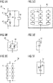
- FIG. 1 shows an exemplary embodiment of a transformer arrangement 10.
- the transformer arrangement 10 comprises a first and a second arrangement side 11, 12 and a transformer 13.
- the transformer 13 includes first windings 14 and second windings 15.
- the second windings 15 have a first to a fourth tap 17 to 20.
- the transformer arrangement 10 comprises a filter arrangement 21 that is connected to the first to the third tap 17 to 18.
- the transformer arrangement 10 comprises a converter 22.
- the converter 22 may be implemented as a power electronic converter.
- the converter 22 is coupled via the filter arrangement 21 to the first, second and third tap 17 to 18.
- the transformer arrangement 10 comprises a filter circuitry 23 coupled to the converter 22 and to the second arrangement side 12.
- the second arrangement side includes a first and a second terminal 24, 25.
- the first terminal 24 of the second arrangement side 12 is coupled via the filter circuitry 23, the converter 22 and the filter arrangement 21 to the first, second and third tap 17 to 19.
- the second terminal 25 of the second arrangement side is connected to the fourth tap 20.
- the filter circuitry 23 can also be named output filter.
- the filter arrangement 21 may include an electromagnetic interference filter, abbreviated EMI filter.
- the filter arrangement 21 may be called input filter.
- a first voltage V1 is tapped.
- a second voltage V2 is tapped.
- the second voltage V2 is tapped between the first and the second terminal 24, 25.
- the first voltage V1 may be realized as a high voltage and the second voltage V2 may be realized as a low voltage.
- the second voltage V2 may be provided to a load.
- a minimum voltage V2min is tapped.
- a difference voltage DV is tapped between the first terminal 24 of the second arrangement side 12 and the second tap 18.
- a first current I1 flows through the first windings 14.
- a second current I2 flows through the second windings 15, especially through the second terminal 25.
- the second current I2 may also be called load current.
- the transformer arrangement 10 includes input and output filters 21, 23.
- the converter 22 implements an on-load PE tap changer.
- input and output filters 21, 23 are provided.
- the filters 21, 23 are designed by using reactors, capacitors and resistors. An input capacitor 21 and output reactor can be enough in many tap-changer cases.
- FIGs 2A and 2B show exemplary embodiments of a transformer arrangement 10 which are further developments of the embodiment shown in Figure 1 .
- the converter 22 comprises a first, a second and a third arm 31, 32, 33.
- the first arm 31 has a first terminal connected to the first tap 17.
- a second terminal of the first arm 31 is coupled to the first terminal 24 of the second arrangement side 12.
- the second arm 32 has a first terminal connected to the second tap 18.
- a second terminal of the second arm 32 is coupled to the first terminal 24 of the second arrangement side 12.
- the third arm 33 has a first terminal connected to the third tap 19.
- a second terminal of the third arm 33 is coupled to the first terminal 24 of the second arrangement side 12.
- the converter 22 can also be named power electronic on-load tap changer AC to AC converter (abbreviated PE OLTC AC-AC converter).
- the first arm 31 includes a first number N1 of cells 29, the second arm 32 includes a second number N2 of cells and the third arm 33 comprises a third number N3 of cells.
- the first number N1 may be equal to the second number N2.
- the third number N3 may be less than the first number N1 and less than the second number N2.
- the transformer arrangement 10 comprises a first filter circuit 34 and a second filter circuit 35.
- the first and second filter circuit 34, 35 form the filter arrangement 21.
- the first and the second filter circuit 34, 35 may be called input filters.
- the first and the second filter circuit 34, 35 each comprises a capacitor 36, 37.
- the second voltage V2 may be named output voltage, transformer output voltage, load voltage or transformer LV output voltage. Continuous and fast regulation of the second voltage V2 can be implemented by the transformer arrangement 10 shown in Figures 2A and 2B .
- the converter 22 allows, within the design margins, to eliminate the traditional step-by-step electromechanical OLTC and to reduce the transformer production cost by eliminating the regulation winding. By removing the regulation winding, the transformer design can be improved to save material and labor cost.
- the topology allows to simplify the requirements on the transformer design and eliminate the electromechanical OLTC to provide at least one of: Fast continuous on-load voltage regulation; mitigation of voltage flickers; phase angle control of the second voltage V2 (the phase angle can be changed within a certain range); and a modified converter cell can work as a circuit breaker.
- FIG. 2A illustrates a basic scheme (with cells 29) and Figure 2B a matrix scheme (with cells 29).
- the first arm 31 includes a matrix 30 (which is explained in Figures 3C and 3D ).
- the second and the third arm 32, 33 each comprises a matrix.
- the converter design will depend on at least one of:
- Figures 3A to 3D show exemplary embodiments of a cell 29 and of a matrix 30 which can be used in the first to the third arm 31 to 33.
- the cell 29 includes a first and a second device 41, 42 and a switch 40 (which may be named by-pass switch).
- the first and the second device 41, 42 are connected in series.
- the first and the second device 41, 42 form an anti-series device connection.
- the first and the second device 41, 42 can be realized as insulated-gate bipolar transistor (abbreviated IGBT).
- the first and the second device 41, 42 are fabricated as metal-oxide-semiconductor field-effect transistor (abbreviated MOSFET).
- the cell 29 comprises a snubber filter 43.
- the snubber filter 43 includes a capacitor.
- the cell 29 is realized without a snubber filter.
- the cell 29 includes a device 44.
- the device 44 is a semiconductor device with bipolar-voltage capability and unidirectional-current capability based on Si or wide-band gap (e.g. SiC) semiconductors.
- the device 44 is e.g. implemented as a phase-controlled thyristor (abbreviated PCT).
- PCT phase-controlled thyristor
- the cell 29 shown in Figure 3B includes a first and a second device that are connected in parallel, for example in an anti-parallel circuit.
- the cell 29 is realized by two anti-parallel devices.
- the matrix 30 includes cells 29 which are connected in serious and/or parallel.
- the cells 29 can be realized such as described above or below.
- different semiconductor device technologies can be used to realize the cell 29 and/or the matrix 30: Si and SiC semiconductor materials and an insulated-gate bipolar transistor (abbreviated IGBT), a metal-oxide-semiconductor field-effect transistor (abbreviated MOSFET) and an integrated gate-commutated thyristor (abbreviated IGCT) semiconductor types.
- IGBT insulated-gate bipolar transistor
- MOSFET metal-oxide-semiconductor field-effect transistor
- IGCT integrated gate-commutated thyristor
- Each arm 31 to 33 includes an anti-series connection of power devices (IGBT and/or MOSFET) as shown e.g. in Figure 3A to 3D , to form switches that can operate in ON - OFF conditions in both current directions and both blocking-voltage polarities, as displayed in Figure 4 .
- IGBT anti-series connection of power devices
- MOSFET MOSFET
- the matrix 30 includes a matrix arrangement of cells 30 having anti-series devices.
- the first, second or third arm 31 to 33 is a series/parallel combination of switches in the form of a matrix arrangement.
- a cell 29 may be realized as a cell 29' of a first type or a cell 29" of a second type.
- the cell 29' of the first type may also be named high-frequency cell.
- the cell 29" of the second type may be named low-frequency cell.
- the cell 29 is implemented as a 4-quadrant switch, abbreviated 4QS.
- the cell 29" of the second type operates at low switching frequency and can be implemented in the following ways:
- the cells 29" of the second type can be interconnected in the following ways: A series connection of cells 29" as shown in Figure 2A or a matrix 30 of such cells 29" (connected in series, parallel or both), as illustrated in Figures 3C and 3D .
- the cell 29' of the first type operates at high switching frequency (abbreviated HF) and can be implemented by semiconductor devices with unipolar-voltage capability and bidirectional-current capability based on Si or wide-band gap (e.g. SiC) semiconductors. Examples of such devices are IGBTs and MOSFETs, as shown in Figure 3A .
- the cells 29' of the first type can be interconnected in the following ways: A series connection of cells 29' as shown in Figure 2A or a matrix 30 of such cells 29' (connected in series, parallel or both), as illustrated in Figures 3C and 3D .
- FIGS 3E and 3F show exemplary embodiments of a first filter circuit 34 which is a further development of the embodiment shown in Figures 2A and 2B .
- the second filter circuit 35, the snubber filter 43, a capacitive element 91, a first and a second internal filter 97, 98 and an internal filter 102 may be realized such as the first filter circuit 34.
- Capacitive filters similar to the first filter circuit 34 are indicated by the letters Fc in the drawings.
- the first filter circuit 34 is a capacitive filter that can be implemented e.g. in the following ways:
- the first filter circuit 34 is e.g. a resistive/capacitive filter.
- the first filter circuit 34 comprises a resistor 45.
- the resistor 45 is connected in series to the capacitor 36. All the above may be combined with the resistor 45 (or a matrix of resistors) connected in series either to each single capacitor or to any combination of capacitors (series, parallel, or both).
- the introduced resistor(s) are useful for damping resonances between the capacitor(s) and inductive elements connected to the first filter circuit 34 or to other capacitive filters.
- Figure 4 show examples of modes of a cell 29 or a matrix 30 described above, namely an equivalent ON - OFF switch of the individual anti-series device or cell arrangement.
- Figures 5A to 5D show examples of modes of a cell 29, described above.
- the normal operation modes of the anti-series switches or cells 29 are shown in Figures 5A, 5B, 5C and 5D . Switches in the ON state and the current path are highlighted with bold lines. Switches in the OFF state and connection lines without current or with a small current are shown with normal lines.
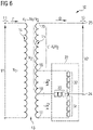
- Figure 6 shows an exemplary embodiment of a transformer arrangement 10 which is a further development of the embodiments shown above.
- the third arm 33 in both cases can be dimensioned for transformer nominal current and for a lower voltage than the other two arms, the first and the second arm 31, 32. During normal operating conditions the losses will be less.
- the second voltage V2 can be regulated within a certain voltage range depending on the design and the three different normal operation modes as described in Figures 7A to 7C .
- one or two arms are conducting.
- LV is the abbreviation for low voltage.
- HV is the abbreviation for high voltage.
- FIG. 6 a single-phase PE OLTC AC-AC converter 22 at LV side is shown. Alternatively, the converter 22 is connected to the HV side.
- the input capacitors have been omitted for clarity.
- the filter arrangement 21, the first and the second filter circuit 34, 35 and the filter circuitry 23 have been omitted for clarity in Figures 6 , 7A to 7C , 8A , 8B , 9, 10 , 11A, 11B , 12 , 13A and 13B .
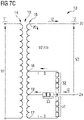
- Figures 7A to 7C show modes of an exemplary embodiment of a transformer arrangement 10 shown above.
- Figures 7A to 7C normal operation modes of the proposed on-load PE tap changer are illustrated.
- mode 1 The first and the third arm 31, 33 are active and switching alternately: V 2 nom ⁇ V 2 ⁇ V 2 max
- mode 2 The second and the third arm 32, 33 are active and switching alternately: V 2 min ⁇ V 2 ⁇ V 2 nom
- V2 is the second voltage.
- V2min is a minimum value of the second voltage and is tapped at the second tap 18.
- V2max is a maximum value of the second voltage and is tapped at the first tap 17.
- V2nom is a nominal value of the second voltage and is tapped at the third tap 19.
- Figures 8A and 8B show an exemplary embodiment of the voltages of a transformer arrangement 10 and a control scheme of a transformer arrangement 10 which is a further development of the embodiments shown above.
- N1 is the number of windings of the first windings 14.
- N2 is the number of windings of the second windings 15 from the third tap 19 to the fourth tap 20.
- n n is a ratio.
- k is a factor less than 1.
- V 2a is a voltage tapped between the second tap 18 and the fourth tap 20.
- V 2b is a voltage tapped between the third tap 19 and the second tap 18.
- V 2c is a voltage tapped between first tap 17 and the second tap 18.
- V 1 n is a nominal value of the first voltage VI.
- the second voltage V2 can be adjusted in less than 1/2 cycle of the grid frequency.
- ⁇ is the duty cycle.
- T sw is a time period being the duration of one cycle.
- t on is a period for conducting of one of the arms 31 to 33.
- FIG 9 shows a further exemplary embodiment of a transformer arrangement 10 which is a further development of the embodiments shown above.
- the transformer arrangement 10 comprises a by-pass switch 50.
- the by-pass switch 50 is realized by two switches 51, 52 such as e.g. two thyristors that are connected in an antiparallel circuit.
- the by-pass switch 50 couples the first terminal 24 of the second arrangement side 12 to a further node such as the first tap 17, the second tap 18 or the third cap 19.
- the converter 22 is protected against external short-circuits currents.
- Anti-parallel thyristors to by-pass the converter during faults can be implemented as displayed in Figure 9 .
- the terminal X can be connected to the nodes A, B or C (depending on the design).
- a by-pass switch 50 or by-pass switches are configured for short-circuit protection (thyristors or other technology can be used).
- basic objectives of the transformer arrangement 10 are e.g. fast and continuous voltage regulation of the transformer; and/or to mitigate voltage flickers.
- the transformer arrangement 10 will be designed according to the rated power of the transformer arrangement 10, the voltage and the system short-circuit current. Main considerations are e.g.:
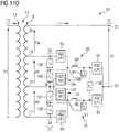
- Figure 10 shows an exemplary embodiment of a transformer arrangement 10 which is a further development of the embodiments shown above.
- the upper range and lower range can be different (DV1 ⁇ DV) as shown in Figure 10 .
- the first number N1 of cells 29 may be different from the second number N2 of cells 29.
- the transformer arrangement 10 realizes a single-phase AC-AC PE converter as OLTC connected at LV side (can also be connected on the HV side).
- FIGs 11A and 11B show exemplary embodiments of a transformer arrangement 10 which is a further development of the embodiments shown above.
- the transformer arrangement 10 can be connected to a ground 54 or reference potential terminal, as explained and shown in Figure 11A or floating as shown in Figure 11B .
- the transformer arrangement 10 can have a grounded PE converter or a floating PE OLTC AC-AC converter.
- the first terminal 24 ( Figure 11A ) of the second arrangement side 12 or the second terminal 25 ( Figure 11B ) of the second arrangement side 12 is connected to the ground 54.
- FIG 12 shows a further exemplary embodiment of a transformer arrangement 10 with three phases which is a further development of the embodiments shown above.
- the transformer arrangement 10 comprises a further transformer 55 that is realized correspondingly to the transformer 13.
- the further transformer 55 comprises first and second windings 56, 57.
- the second windings 57 include a first to a fourth tap 58 to 61.
- the transformer arrangement 10 comprises a further converter 62 coupled to the first, second and third tap 58 to 60.
- the second side 12 of the transformer arrangement 10 comprises a third terminal 63.
- a terminal of the further converter 62 is connected to the first terminal 24 of the second arrangement side 12.
- the transformer arrangement 10 comprises an additional transformer 70 with first and second windings 71, 70.
- the second windings 72 include a first to a fourth tap 73 to 76.
- the transformer arrangement 10 comprises an additional converter 77 that is connected to the first, second and third tap 73 to 75.
- a terminal of the additional converter 77 is connected to the first terminal 24 of the second arrangement side 12.
- a fourth terminal 78 of the second arrangement side 12 is connected to the fourth tap 76.
- three phases a, b and c can be tapped at the second, the third and the fourth terminal 25, 36, 78.
- a neutral phase n may be tapped at the first terminal 24 of the second arrangement side 12.
- a third voltage V3 is provided to the first windings 56 of the further transformer 55.
- the further converter 62 generates a fourth voltage V4.
- a fifth voltage V5 is provided to the first windings 71 of the additional transformer 70.
- the additional converter 77 generates a sixth voltage V6. Voltage differences DV4, DV6 and minimum voltages V4min, V6min can be tapped at the further converter 62 and the additional converter 77.
- the converter 22 for a single-phase transformer can be used in three phase transformer banks, or three phase transformers in any of its connections: star-delta YD, delta-star DY, delta-delta DD or star-star YY, or other as well as at the HV side or LV side.
- three-phase connection (YY) of the transformed arrangement 10 is realized at LV side.
- Other three-phase connections as YD, DY and DD are also possible.
- Connection of the converter 22, 52, 77 at HV side is also possible.
- FIGs 13A and 13B show exemplary embodiments of a transformer arrangement 10 with a tank 80 which is a further development of the embodiments shown above.
- the transformer arrangement 10 comprises a box 80.
- the converter 22 is inserted in the box 18.
- the first and the second filter circuit 34, 35 and the filter circuitry 23 may also be inserted into the box 18.
- the transformer arrangement 10 comprises a tank 81.
- the transformer 13 is inserted into the tank 81.
- the box 80 is also inserted into the tank 81.
- the box 80 is not inserted into the tank 81.
- the box 80 is outside of the tank 81.
- the tank 81 is free from the box 80.
- the transformer arrangement 10 comprises bushings 82 to 84 that couple the tank 81 to the box 80.
- the bushings 82 to 84 couple the first to the third tap 17 to 18 to the converter 22.
- the OLTC AC-AC PE converter 22 can be built as a separate unit and connected to the transformer 13 in a substation, it can also be integrated inside the transformer tank 81 or assembled in an external box 80 which can be named container as a modular backpack solution as shown in Figures 13A and 13B respectively.
- container can be named container as a modular backpack solution as shown in Figures 13A and 13B respectively.
- the transformer 13 and the converter 22 are mounted in the same tank 81.
- the transformer 13 and the converter 22 are realized in a backpack modular solution.
- FIGS 14A to 14D show different exemplary embodiments of a transformer arrangement 10 which are further developments of the embodiments shown above.
- the PE converter 22 shown in Figures 1 , 2A and 2B represents one way of implementing the basic function of voltage regulation by employing three transformer taps 17 to 19.
- the same functionality can be implemented by other circuit variations, which are briefly described in the following paragraphs and figures.
- the symbols depicted and defined e.g. in Figures 3A to 3F are used for describing the circuit variations. A short description of each variation is summarized as follows.
- FIG 14A shows an exemplary embodiment of a transformer arrangement 10 which is a further developments of the embodiments shown above.
- the transformer arrangement 10 represents a variation of the initial circuit shown in Figures 1 , 2A and 2B .
- each arm 31 to 33 is represented by the 4QS symbol (defined and described in Figures 3A to 3D ) and the filter arrangement 21 and the filter circuitry 23 have been added.
- the first and the second filter circuit 34, 35 form the filter arrangement 21, also named input filter.
- the filter arrangement 21 is mainly capacitive. As shown in Figure 3F , the filter arrangement 21 may include resistive elements, introduced for damping electrical resonances.
- the filter circuitry 23 coupling the converter 22 to the second side 12 of the transformer arrangement 10 is a low-pass filter.
- the filter circuitry 23 comprises an inductive element 90 and a capacitive element 91 such as shown in Figures 2E and 2F (with possibility to introduce resistive elements for damping oscillations between the inductive element 90 and the capacitive element 91 of the filter circuitry 23).
- This is only one potential filter implementation. Other implementations are possible.
- the lower terminal of the capacitive element 91 of the filter circuitry 23 is connected to a neutral point NP.
- the neutral point NP is connected to the third tap 19.
- this circuit variation represents the circuit shown in Figure 2A complemented with a low-pass LC filter 23 for filtering out the switching harmonics of the converter 22.
- the capacitive element 91 and the first and the second filter 34, 35 can be realized as the first filter 34, explained in Figures 3E and 3F and in the description of Figures 3E and 3F and as indicated by the letters Fc.
- the first to the third arm 31 to 33 are each implemented by at least a four-quadrant switch, as explained together with Figures 3A to 3D and as indicated by the letters 4QS.
- the first arm 31 is realized by a cell 29 (as shown e.g. in Figures 3A and 3B ), a series circuit of cells 29 (as shown in Figure 2A ) or a matrix 30 of cells 29 (as shown in Figure 2B , 3C and 3D ).
- the second and the third arm 32, 33 are realized such as the first arm 31.
- Figure 14B shows an exemplary embodiment of a transformer arrangement 10 which is a further developments of the embodiments shown above.
- the circuit variation shown in Figure 14B is based on the one shown in Figure 14A .
- the upper and lower arms i.e. the first and the second arm 31, 32 are split in two parts; notably, one part 92, 94 is operating at low switching frequency (abbreviated LF) and one part 93, 95 is operating at high switching frequency (abbreviated HF).
- LF low switching frequency
- HF high switching frequency
- the first arm 31 comprises a first LF part 92 and a first HF part 93.
- the second arm 32 comprises a second LF part 94 and a second HF part 95.
- the third arm 33 comprises a third HF part 96.
- the first and the second LF part 92, 94 include a cell 29" of the second type.
- the first, the second and the third HF part 93, 95, 96 include a cell 29' of the first type.
- LF is the abbreviation for low frequency
- HF is the abbreviation for high frequency.
- a HF part can be named part of a first type.
- a LF part can be named part of a second type.
- the HF part or HF parts are realized different from the LF part or LF parts.
- This variation is different to the initial circuit shown in Figure 2A in terms of operation, in the sense that the first, the second and the third HF part 93, 95, 96 regulate the second voltage V2, while the first and the second LF part 92, 94 clamp the HF parts 93, 95 to one of the auxiliary windings.
- all switching operations are realized by the first, second and third HF parts 93, 95, 96, while the first and the second LF parts 92, 94 are continuously in a conducting state (they are ON).
- one of the first and the second LF part 92, 94 is in a conducting state, while the other of the first and the second LF part 92, 94 is in a non-conducting state.
- the operation of this transformer arrangement 10 is briefly described in Figures 15A to 15C .
- a HF part or a LF part can be realized by a cell 29 (as shown e.g. in Figures 3A and 3B ), a series circuit of cells 29 (as shown in Figure 2A ) or a matrix 30 of cells 29 (as shown in Figure 2B , 3C and 3D ).
- a HF part is indicated by the letters 4QS [HF] and a LF part is indicated by the letters 4QS [LF] in the drawings 14B to 14D.
- the total voltage rating of semiconductor devices is the same, and if the second voltage V2 has to be equal to the nominal voltage V2nom, the third arm 33 (called middle arm) offers a path with low conduction losses.
- the filter circuitry 23, called output L-Fc filter can be connected to the neutral point NP or another terminal, e.g. the second tap 18 (called upper terminal of the top auxiliary winding) or the first tap 17 (called lower terminal of the bottom auxiliary winding).
- the converter 22 comprises a first and a second internal filter 97, 98.
- the first and the second internal filter 97, 98 are implemented e.g. such as the first filter circuit 34.
- the first and the second internal filter 97, 98 may be low-pass filters.
- the first internal filter 97 couples the node between the first LF part 92 and the first HF part 93 of the first arm 31 to the neutral point NP.
- the second internal filter 98 couples the node between the second LF part 94 and the second HF part 95 of the second arm 32 to the neutral point NP.
- the internal filter 97, 98 can be introduced for reducing the voltage stress (e.g. as snubber) of the HF components during switching operations.
- the internal filter 97, 98 are optional, as denoted by dashed lines in Figure 14B .
- the converter 22 splits the first and the second arm 31, 32 in two parts: one that operates at low switching frequency [LF] and one that operates at high switching frequency [HF].
- Input and output capacitors can be replaced by capacitors connected in series with resistors (see Figures 3E and 3F ).
- Figure 14C shows an exemplary embodiment of a transformer arrangement 10 which is a further development of the embodiments shown above.
- the third arm 33 couples the third tap 19 to a node of the first arm 31.
- the node is located between the first LF part 92 and the first HF part 93 of the first arm 31.
- the third arm 33 comprises a LF part 99.
- the converter 22 comprises a fourth arm 100 that couples the third tap 19 to a node of the second arm 32.
- the node is arranged between the second LF part 94 and the second HF part 95 of the second arm 32.
- the fourth arm 100 comprises a LF part 101.
- the transformer arrangement 10 shown in Figure 14C is based on the structure of an active neutral-point clamp converter.
- the parallel connection of two LF-HF branches can offer a path with low conduction losses.
- the converter 22 may comprise an internal filter 102 that may be realized as the first filter circuit 43, shown in Figures 3E or 3F . Yet, if the optional internal filter 102 is present, the activation of this path is done with care for avoiding inrush currents due to discharging of the capacitor of the internal filter 102 (e.g. activation can be performed at the zero crossing of the voltage across the internal filter 102).
- this variation offers the opportunity to minimize total losses by employing different devices.
- devices optimized for low conduction losses e.g. IGBTs of voltage classes 4.5, 6.5 kV, BIGTs, PCTs, BCTs
- devices optimized for low switching losses e.g. Si-based IGBTs of voltage classes 1.2, 1.7 kV, SiC-based IGBTs, SiC-based MOSFETs
- Si-based IGBTs of voltage classes 1.2, 1.7 kV, SiC-based IGBTs, SiC-based MOSFETs can be used for the HF parts 93, 95.
- the total voltage rating of semiconductor devices for this circuit variation is higher than that of the circuit variation of Figures 14A and 14B .
- the filter circuitry 23 (named output L-Fc filter) can be connected to the neutral point NP or other terminals, e.g. the second tap 18 (upper terminal of the top auxiliary winding) or the first tap 17 (lower terminal of the bottom auxiliary winding), or to one of the midpoints between the upper or lower LF and HF parts.
- the optional internal filter 102 (denoted by dashed lines in Figure 14C ) can be introduced for reducing the voltage stress (e.g. as snubber) of the HF components during switching operations.
- the circuit variation is based on active neutral-point clamped structure.
- the HF parts 93, 95 perform voltage regulation, while the LF parts 92, 94, 199, 101 clamp the HF part 93, 95 to either of the two auxiliary windings of voltage ⁇ v.
- Figure 14D shows an exemplary embodiment of a transformer arrangement 10 which is a further development of the embodiments shown above.
- the transformer arrangement 10 shown in Figure 14D is based on the one of in Figure 14C , but the placement of the HF and LF parts is swapped, i.e. the HF parts are now placed closer to the taps 17 to 19 (i.e. closer to the auxiliary windings).
- the change does not have any implication to the total voltage rating of semiconductor devices compared to the circuit variation of Figure 14C . Yet, it has an impact on the internal filters 97, 98.
- the converter 22 comprises the first and the second internal filter 97, 98.
- the first internal filter 97 is coupled via the first HF part 93 of the first arm 31 to the first tap 17 and via the third arm 33 to the third tap 19.
- the first internal filter 97 is coupled via the first LF part 92 of the first arm 31 to the first terminal 24 of the second arrangement side 12.
- the third arm 33 includes a HF part 103.
- the second internal filter 98 is coupled via the second part 95 of the second arm 32 to the second tap 18 and via the fourth arm 100 to the third tap 19.
- the fourth arm 100 comprises a HF part 104.
- the second internal filter 98 is coupled via the second LF part 94 of the second arm 33 to the first terminal 24 of the second arrangement side 12.
- the first and the second internal filter 97, 98 each include an inductive element 90, 90' and an capacitive element 91, 91'
- the first and the second internal filter 97, 98 are arranged close to the HF parts 93, 95, 103, 104 for filtering the harmonics of the HF parts 93, 95, 103, 104.
- the first and the second internal filter 97, 98 replace the filter circuitry 23 or the output L-Fc filters.
- One terminal of the first internal filter 97 is connected to a point B.
- One terminal of the second internal filter 98 is connected to a point A.
- the potential of these points A, B may be floating with respect to the neutral phase NP and in an example may become equal to ⁇ v.
- larger input capacitance may be required compared to the circuit variation of Figure 14C .
- the aforementioned terminals of the L-Fc filters connected to points A and B can alternatively be connected either to the first and the second tap 17, 18 (lower terminal of the bottom auxiliary winding and upper terminal of the top auxiliary winding) or both to the neutral point or neutral phase NP.
- the first filter circuit 34 comprises a first and a second filter element 106, 107 connected to each other via the point B in a series connection.
- the second filter circuit 35 comprises a third and a fourth filter element 108, 109 connected to each other via the point A in a series connection.
- FIG. 17A and 17B The internal filter 102 is optional (denoted by dashed lines in Figure 14B ) and can be introduced for reducing the voltage stress (e.g. as snubber) of the HF components during switching operations.
- the transformer arrangement 10 is based on an active neutral-point clamped structure, but differs from the circuit variation in Figure 14C in terms of the location of the LF and HF parts.
- the HF part that performs voltage regulation is located closer to the auxiliary windings; the LC filters 97, 98 required to filter the HF harmonics are placed close to the HF parts of the converter 22.
- the power electronic AC-AC converter topology allows transformer voltage and flicker mitigation.
- the converter 22 can be assembled using anti-series connected Si/SiC based devices such as IGBTs, BIGTs, and/or MOSFETs, etc..
- the control strategy includes three operation modes (see Figures 7A to 7C ).
- the converter 22 is assembled in the same tank 81 of the transformer 13 or as a backpack modular solution outside of the tank 81 of the transformer 13 ( Figures 13A and 13B ) (or as a separate unit).
- the circuit variations presented in Figure 14A to 14D implement the same function as the circuit variation shown in Figures 1 , 2A and 2B .
- the transformer arrangement 10 has benefits, such that it is faster, cheaper, safer etc..
- the transformer arrangement 10 performs a replacement of the step-by-step traditional electromechanical OLTC; there are simplified design requirements for the transformer 13 (transformer design simplification); transformer manufacturing costs are reduced (mechanical design, less additional windings); power electronic losses are reduced compared with prior art; the transformer arrangement realizes and improved compactness of unified transformer-PE block compared with conventional OLTC solution; the transformer arrangement 10 includes extended functionalities of the transformer (i.e. flicker mitigation).
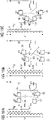
- Figures 15A to 15C show examples of modes of a transformer arrangement 10 of Figure 14B . Illustration of operation of circuit variation is shown in Figure 14B .
- the second voltage V2 should be in the range 0.9 to 1 p.u. (p.u. means that the second voltage V2 is provided in the per-unit system).
- the second LF part 94 of the second arm 32 is continuously on.
- the second HF part 95 of the second arm 32 and the third HF part 96 of the third arm 33 are switching.
- the second voltage V2 should be in the range 1.0 to 1.1 p.u.
- the first LF part 92 of the first arm 31 is continuously on.
- the first HF part 93 of the first arm 31 and the third HF part 96 of the third arm 33 are switching.
- the second voltage V2 should be about 1.0 p.u.
- the third HF part 96 of the third arm 33 is on.
- An output filter impedance is inserted in the current path.
- Figures 16A to 16C shows examples of modes of a transformer arrangement of Figure 14C .
- the second voltage V2 should be in the range 0.9 to 1 p.u.
- the upper auxiliary windings having the second and the third tap 18, 19 are connected to HF parts 93, 95 by two LF parts 94, 99 being continuously on.
- the HF parts 93, 95 are switching to regulate the second voltage V2.
- the second voltage V2 should be in the range 1.0 to 1.1 p.u.
- the lower auxiliary windings having the first and the third tap 17, 19 are connected to HF parts 93, 95 by two LF parts 94, 101 which are continuously on.
- the HF parts 93, 95 are switching to regulate the second voltage V2.
- the second voltage V2 should be about 1.0 p.u. Low conduction losses are achieved by parallel-connected LF and HF parts. Activation of this path is done carefully to avoid short of dashed capacitors. Input and output capacitors can be replaced by capacitors connected in series with resistors (see Figures 3E and 3F ).
- FIGs 17A and 17B show exemplary modes of a transformer arrangement 10 of Figure 14D .
- Input and output capacitors can be replaced by capacitors connected in series with resistors (see Figures 3E and 3F ).
- the second voltage V2 should be in the range 0.9 to 1 p.u.
- the HF parts 95, 104 of the second and the fourth arm 32, 100 are switching to regulate the second voltage V2.
- the second LF part 94 of the second arm 32 is continuously on.
- the second voltage V2 should be in the range 1.0 to 1.1 p.u.
- the HF parts 93, 103 of the first and the third arm 31, 33 are switching to regulate the second voltage V2.
- the first LF part 92 of the first third arm 31 is continuously on.
Landscapes
- Engineering & Computer Science (AREA)
- Power Engineering (AREA)
- Ac-Ac Conversion (AREA)
- Control Of Electrical Variables (AREA)
- Inverter Devices (AREA)
Abstract
Description
- The disclosure is related to a transformer arrangement and a method for voltage conversion.
- A transformer arrangement performs on AC to AC conversion. Since the number of windings on a first side and on a second side of the transformer are constant, also the conversion rate is constant. In order to vary the conversion rate, an on-load tap changer, abbreviated OLTC, can be used. However, an OLTC results in high manufacturing costs and can only be used to realize distinct values of the conversion rate.
- Document
US 2013/0207471 A1 describes imputed DC link cell-based power converters. A power converter comprise a transformer having first windings and second windings with four taps. Three taps are coupled by imputed DC link cells and an output filter inductor to an output of the power converter. - Document
US 2016/0099653 A1 describes a power flow controller with a fractionally rated back-to-back converter. A transformer has second windings with four taps. Two of the four taps are coupled by a converter to an output of the arrangement. - It is an object to provide a transformer arrangement and a method for voltage conversion with a high flexibility of the conversion rate.
- The object is achieved by the subject matter of the independent claims. Further developments are described in the dependent claims.
- There is provided a transformer arrangement which comprises a first and a second arrangement side, a transformer, a converter and a first and a second filter circuit. The transformer comprises first windings coupled to the first arrangement side and second windings having a first, a second, a third and a fourth tap. The converter couples the first, second and third tap to the second arrangement side. The first filter circuit couples the first tap to the third tap. The second filter circuit couples the third tap to the second tap.
- Advantageously, the converter receives three voltages on its input side and is able to generate a second voltage using these three voltages. A first voltage is tapped at the first arrangement side. The second voltage is tapped at the second arrangement side. The second voltage may be an output voltage. The second voltage can have several different values. A conversion rate of the transformer arrangement can be controlled.
- The first arrangement side may be a high-voltage side and the second arrangement side may be a low-voltage side; the first voltage is higher than the second voltage. Alternatively, the first arrangement side may be the low-voltage side and the second arrangement side may be the high-voltage side; the first voltage is lower than the second voltage.
- The first arrangement side may be a source side and the second arrangement side may be a load side. Thus, the first arrangement side may be coupled to a source such as a grid and the second arrangement side may be coupled to a load such as a motor of further grid.
- Alternatively, the first arrangement side may be a load side and the second arrangement side may be a source side. Thus, the first arrangement side may be coupled to a load and the second arrangement side may be coupled to a source.
- In a development of the transformer arrangement, the converter comprises a first arm comprising a first number of cells and a first terminal connected to the first tap, a second arm comprising a second number of cells and a first terminal connected to the second tap and a third arm comprising a third number of cells and a first terminal connected to the third tap. Advantageously, the first, second and third tap are each connected to a separate arm. By controlling the three arms the generation of the second voltage as a function of the voltages tapped at the tree taps can be tuned.
- In a development, the transformer arrangement comprises a filter circuitry. The filter circuitry may be implemented as a low-pass filter. The filter circuitry couples the converter to the second arrangement side. Advantageously, the filter circuitry achieves a smoothing of the second voltage.
- In the development of the transformer arrangement, a second terminal of the first arm, a second terminal of the second arm and a second terminal of the third arm are coupled via the filter circuitry to a first terminal of the second arrangement side. Thus, the first, second and third arm are connected to one terminal of the filter circuitry and another terminal of the filter circuitry is coupled to the first terminal of the second arrangement side.
- In a development of the transformer arrangement, the filter circuitry includes a capacitive element connected to the third tap. Moreover, the filter circuitry comprises an inductive element.
- In a development of the transformer arrangement, the fourth tap of the second windings is coupled to the second arrangement side. The fourth tap is connected or coupled to a second terminal of the second arrangement side.
- In a development of the transformer arrangement, the converter comprises a fourth arm comprising a fourth number of cells and a first terminal connected to the third tap. A second terminal of the third arm is connected to a node of the first arm. A second terminal of the fourth arm is connected to a node of the second arm. A second terminal of the first arm and a second terminal of the second arm are coupled to a first terminal of the second arrangement side. Advantageously, by using the third and the fourth arm the second voltage can be generated with high flexibility.
- In a development of the transformer arrangement, the first arm includes a first internal filter. The second arm includes a second internal filter. Advantageously, the second voltage tapped at the first terminal of the second arrangement side is smoothed by the first and the second internal filter.
- In a development of the transformer arrangement, the third number of cells is less than the first number of cells and is less than the second number of cells. Advantageously, a voltage across the third arm is less than a voltage across the first arm and a voltage across the second arm. The converter can be realized using a smaller number of cells for the third arm in comparison to the first and second arm.
- In a development of the transformer arrangement, the first number of cells is equal to the second number of cells. Advantageously, a maximum value of a voltage across the first arm and a maximum value of a voltage across the second arm are equal.
- In a development of the transformer arrangement, a cell comprises a device of a group comprising a metal-oxide-semiconductor field-effect transistor (abbreviated MOSFET), an insulated-gate bipolar transistor (IGBT), a reverse-conducting insulated-gate bipolar transistor (RC-IBGT), a thyristor and a bi-mode insulated gate transistor (BIGT). Advantageously, the devices of this group allow to set the cell in a conducting and a non-conducting state.
- In a development of the transformer arrangement, the thyristor may be one of a phase-controlled thyristor (PCT), a bidirectional-controlled thyristor (BCT) and an integrated gate-commutated thyristor (IGCT).
- In a development of the transformer arrangement, the first number of cells of the first arm includes at least a cell of a first type and a cell of a second type. The second number of cells of the second arm includes at least a cell of a first type and a cell of a second type. The cell of the first type is realized as a high-frequency cell and the cell of the second type is realized a low-frequency cell. The cell of the first type and the cell of the second type are realized in a different manner, i.e. they include different devices, e.g. as listed above. The cell of a first type is configured for operation at higher frequencies as the cell of a second type. In an example, low switching frequencies or an operating range of a low-frequency cell may be from 20 Hz to 1 kHz or from 50 Hz to 600Hz or from 60 Hz to 500 Hz. In an example, high switching frequencies or an operating range of a high-frequency cell may be from 0.4 kHz to 200 kHz or from 0.6 to 100 kHz. These are only examples of ranges. There may be an overlap between a range of the high-frequency cell and a range of the low-frequency cell.
- In a development of the transformer arrangement, a cell of a first type (also named HF cell) includes e.g. wide-bandgap devices (abbreviated WBG devices) and/or devices optimized for low switching losses. The devices can be either transistors or thyristors.
- In a development of the transformer arrangement, a cell of a second type (also named LF cell) includes devices optimized for low conduction losses. The devices can be either transistors or thyristors.
- In a development, the transformer arrangement comprises a by-pass switch coupling the first terminal of the second arrangement side to one of a group comprising the first, the second and the third tap. The by-pass switch can be used for short circuit protection. The by-pass switch may include a thyristor or another switch.
- In a development, the transformer arrangement comprises a box in which the converter is arranged and a tank in which the transformer and the box are arranged. Advantageously, one cooling system is used for the converter and for the transformer.
- In a development, the transformer arrangement comprises a box in which the converter is arranged, a tank in which the transformer is arranged and bushings that couple at least the first, the second and the third tap to the converter. Advantageously, the tank is separated from the box. The box is not inside in the tank. Thus, a maintenance or replacement of the converter can be performed separately from a maintenance or replacement of the transformer.
- There is provided a method for voltage conversion which comprises:
- providing a first voltage to first windings of a transformer,
- generating voltages at a first to a fourth tap of second windings of the transformer,
- providing a second voltage by a converter coupled to the first, second and third tap,
- filtering a voltage between the first tap and the third tap by a first filter circuit, and
- filtering a voltage between the third tap and the second tap by a second filter circuit.
- Advantageously, the voltage between the first tap and the third tap is smoothed by the first filter circuit. Correspondingly, the voltage between the third tap and the second tap is smoothed by the second filter circuit. By controlling the converter, the second voltage can be set on a predetermined value. The first and the second voltage are AC voltages.
- The transformer arrangement is particularly suitable for the method for voltage conversion. Features described in connection with the transformer arrangement can therefore be used for the method and vice versa.
- In a development, the transformer arrangement realizes a power electronic AC-AC converter as OLTC for transformer voltage regulation. Power electronic (sometimes called power electronics) is abbreviated PE. The converter can be implemented as power electronic converter, abbreviated PE converter. The power electronic AC-AC converter topology shows benefits in terms of on-load voltage regulation to replace the traditional electromechanical OLTC of the transformer to reduce the transformer manufacturing cost and to improve the functionalities. The transformer arrangement implements a regulation of the power transformer voltage and/or the power flow through the transformer, e.g. by a stepped or step-less voltage control.
- The following description of figures of examples or embodiments may further illustrate and explain aspects of the transformer arrangement and the method for voltage conversion. Arrangements, devices, circuits and cells with the same structure and the same effect, respectively, appear with equivalent reference symbols. In so far as arrangements, devices, circuits and cells correspond to one another in terms of their function in different figures, the description thereof is not repeated for each of the following figures.
-
Figures 1 ,2A and 2B show exemplary embodiments of a transformer arrangement; -
Figures 3A to 3D show exemplary embodiments of a cell andFigures 3E and 3F show exemplary embodiments of a filter circuit; -
Figures 4 and 5A to 5D show examples of modes of a cell; -
Figures 6 ,7A to 7C ,8A ,8B ,9, 10 ,11A and 11B show exemplary embodiments of transformer arrangements; -
Figure 12 shows a further exemplary embodiment of a transformer arrangement with three phases; -
Figures 13A and 13B show exemplary embodiments of a transformer arrangement with a tank; -
Figures 14A to 14D show different exemplary embodiments of a transformer arrangement; and -
Figures 15A to 15C ,16A to 16C ,17A and 17B show exemplary modes of a transformer arrangement. -
Figure 1 shows an exemplary embodiment of atransformer arrangement 10. Thetransformer arrangement 10 comprises a first and asecond arrangement side transformer 13. Thetransformer 13 includesfirst windings 14 andsecond windings 15. Thesecond windings 15 have a first to afourth tap 17 to 20. Thetransformer arrangement 10 comprises afilter arrangement 21 that is connected to the first to thethird tap 17 to 18. Additionally, thetransformer arrangement 10 comprises aconverter 22. Theconverter 22 may be implemented as a power electronic converter. Theconverter 22 is coupled via thefilter arrangement 21 to the first, second andthird tap 17 to 18. Thetransformer arrangement 10 comprises afilter circuitry 23 coupled to theconverter 22 and to thesecond arrangement side 12. The second arrangement side includes a first and asecond terminal first terminal 24 of thesecond arrangement side 12 is coupled via thefilter circuitry 23, theconverter 22 and thefilter arrangement 21 to the first, second andthird tap 17 to 19. Thesecond terminal 25 of the second arrangement side is connected to thefourth tap 20. Thefilter circuitry 23 can also be named output filter. Thefilter arrangement 21 may include an electromagnetic interference filter, abbreviated EMI filter. Thefilter arrangement 21 may be called input filter. - At the
first arrangement side 11, a first voltage V1 is tapped. At thesecond arrangement side 12, a second voltage V2 is tapped. The second voltage V2 is tapped between the first and thesecond terminal second tap 18 and the fourth tap 20 a minimum voltage V2min is tapped. A difference voltage DV is tapped between thefirst terminal 24 of thesecond arrangement side 12 and thesecond tap 18. A first current I1 flows through thefirst windings 14. A second current I2 flows through thesecond windings 15, especially through thesecond terminal 25. The second current I2 may also be called load current. - In
Figure 1 , thetransformer arrangement 10 includes input andoutput filters converter 22 implements an on-load PE tap changer. Depending on the rated power and design requirements of thetransformer arrangement 10, which includes requirements e.g. for maximum harmonic content, input andoutput filters filters input capacitor 21 and output reactor can be enough in many tap-changer cases. -
Figures 2A and 2B show exemplary embodiments of atransformer arrangement 10 which are further developments of the embodiment shown inFigure 1 . Theconverter 22 comprises a first, a second and athird arm first arm 31 has a first terminal connected to thefirst tap 17. A second terminal of thefirst arm 31 is coupled to thefirst terminal 24 of thesecond arrangement side 12. Thesecond arm 32 has a first terminal connected to thesecond tap 18. A second terminal of thesecond arm 32 is coupled to thefirst terminal 24 of thesecond arrangement side 12. Correspondingly, thethird arm 33 has a first terminal connected to thethird tap 19. A second terminal of thethird arm 33 is coupled to thefirst terminal 24 of thesecond arrangement side 12. Theconverter 22 can also be named power electronic on-load tap changer AC to AC converter (abbreviated PE OLTC AC-AC converter). - As shown in
Figure 2A , thefirst arm 31 includes a first number N1 ofcells 29, thesecond arm 32 includes a second number N2 of cells and thethird arm 33 comprises a third number N3 of cells. The first number N1 may be equal to the second number N2. The third number N3 may be less than the first number N1 and less than the second number N2. - The
transformer arrangement 10 comprises afirst filter circuit 34 and asecond filter circuit 35. The first andsecond filter circuit filter arrangement 21. The first and thesecond filter circuit second filter circuit capacitor - The second voltage V2 may be named output voltage, transformer output voltage, load voltage or transformer LV output voltage. Continuous and fast regulation of the second voltage V2 can be implemented by the
transformer arrangement 10 shown inFigures 2A and 2B . Theconverter 22 allows, within the design margins, to eliminate the traditional step-by-step electromechanical OLTC and to reduce the transformer production cost by eliminating the regulation winding. By removing the regulation winding, the transformer design can be improved to save material and labor cost. The topology allows to simplify the requirements on the transformer design and eliminate the electromechanical OLTC to provide at least one of: Fast continuous on-load voltage regulation; mitigation of voltage flickers; phase angle control of the second voltage V2 (the phase angle can be changed within a certain range); and a modified converter cell can work as a circuit breaker. - The
transformer arrangement 10 realizing a PE OLTC AC/AC converter topology is shown inFigures 2A and 2B. Figure 2A illustrates a basic scheme (with cells 29) andFigure 2B a matrix scheme (with cells 29). InFigure 2B , thefirst arm 31 includes a matrix 30 (which is explained inFigures 3C and 3D ). Correspondingly, the second and thethird arm - The converter design will depend on at least one of:
- Voltage and current requirements;
- Device voltage class and device current class;
- Design factors and margins; and/or
- Required reliability (redundancy).
-
Figures 3A to 3D show exemplary embodiments of acell 29 and of amatrix 30 which can be used in the first to thethird arm 31 to 33. - In
Figure 3A , thecell 29 includes a first and asecond device 41, 42 and a switch 40 (which may be named by-pass switch). The first and thesecond device 41, 42 are connected in series. The first and thesecond device 41, 42 form an anti-series device connection. The first and thesecond device 41, 42 can be realized as insulated-gate bipolar transistor (abbreviated IGBT). Alternatively, the first and thesecond device 41, 42 are fabricated as metal-oxide-semiconductor field-effect transistor (abbreviated MOSFET). Thecell 29 comprises asnubber filter 43. Thesnubber filter 43 includes a capacitor. Alternatively, thecell 29 is realized without a snubber filter. - In
Figure 3B , thecell 29 includes adevice 44. Thedevice 44 is a semiconductor device with bipolar-voltage capability and unidirectional-current capability based on Si or wide-band gap (e.g. SiC) semiconductors. Thedevice 44 is e.g. implemented as a phase-controlled thyristor (abbreviated PCT). Alternatively, thecell 29 shown inFigure 3B includes a first and a second device that are connected in parallel, for example in an anti-parallel circuit. Thus, thecell 29 is realized by two anti-parallel devices. - In
Figures 3C and 3D , thematrix 30 includescells 29 which are connected in serious and/or parallel. Thecells 29 can be realized such as described above or below. In general, different semiconductor device technologies can be used to realize thecell 29 and/or the matrix 30: Si and SiC semiconductor materials and an insulated-gate bipolar transistor (abbreviated IGBT), a metal-oxide-semiconductor field-effect transistor (abbreviated MOSFET) and an integrated gate-commutated thyristor (abbreviated IGCT) semiconductor types. Thematrix 30 e.g. includes at least twocells 29 that are connected in parallel. - Each
arm 31 to 33 includes an anti-series connection of power devices (IGBT and/or MOSFET) as shown e.g. inFigure 3A to 3D , to form switches that can operate in ON - OFF conditions in both current directions and both blocking-voltage polarities, as displayed inFigure 4 . - In
Figure 2B andFigures 3C and 3D , the same concept is elucidated using a series and/or parallel connection of the switches orcells 29 to design thematrix 30 in order to increase the current and/or voltage converter requirements and/or to improve the system reliability. Thematrix 30 also operates as ON - OFF switches in both current directions and both blocking-voltage polarities, as shown inFigure 4 . - In
Figure 3C , thematrix 30 includes a matrix arrangement ofcells 30 having anti-series devices. The first, second orthird arm 31 to 33 is a series/parallel combination of switches in the form of a matrix arrangement. - A
cell 29 may be realized as a cell 29' of a first type or acell 29" of a second type. The cell 29' of the first type may also be named high-frequency cell. Thecell 29" of the second type may be named low-frequency cell. - The
cell 29 is implemented as a 4-quadrant switch, abbreviated 4QS. - The
cell 29" of the second type operates at low switching frequency and can be implemented in the following ways: - By employing semiconductor devices with unipolar-voltage capability and bidirectional-current capability based on Si or wide-band gap (e.g. SiC) semiconductors. Examples of such devices are IGBTs and MOSFETs, as shown in
Figure 3A . - By employing semiconductor devices with bipolar-voltage capability and unidirectional-current capability based on Si or wide-band gap (e.g. SiC) semiconductors. A phase-controlled thyristor (PCT) is an example of such device.
- By employing semiconductor devices with bipolar-voltage and bidirectional-current capabilities based on Si or wide-band gap (e.g. SiC) semiconductors. A bidirectional-controlled thyristor (abbreviated BCT) is an example of such a device, as shown in
Figure 3B . - The
cells 29" of the second type can be interconnected in the following ways: A series connection ofcells 29" as shown inFigure 2A or amatrix 30 ofsuch cells 29" (connected in series, parallel or both), as illustrated inFigures 3C and 3D . - The cell 29' of the first type operates at high switching frequency (abbreviated HF) and can be implemented by semiconductor devices with unipolar-voltage capability and bidirectional-current capability based on Si or wide-band gap (e.g. SiC) semiconductors. Examples of such devices are IGBTs and MOSFETs, as shown in
Figure 3A . The cells 29' of the first type can be interconnected in the following ways: A series connection of cells 29' as shown inFigure 2A or amatrix 30 of such cells 29' (connected in series, parallel or both), as illustrated inFigures 3C and 3D . -
Figures 3E and 3F show exemplary embodiments of afirst filter circuit 34 which is a further development of the embodiment shown inFigures 2A and 2B . Thesecond filter circuit 35, thesnubber filter 43, acapacitive element 91, a first and a secondinternal filter first filter circuit 34. Capacitive filters similar to thefirst filter circuit 34 are indicated by the letters Fc in the drawings. - The
first filter circuit 34 is a capacitive filter that can be implemented e.g. in the following ways: -
Single capacitor 36, as shown inFigure 3E . - Parallel-connected capacitors.
- Series-connected capacitors.
- Matrix of series-parallel-connected capacitors.
- As shown in
Figure 3F , thefirst filter circuit 34 is e.g. a resistive/capacitive filter. Thefirst filter circuit 34 comprises aresistor 45. Theresistor 45 is connected in series to thecapacitor 36. All the above may be combined with the resistor 45 (or a matrix of resistors) connected in series either to each single capacitor or to any combination of capacitors (series, parallel, or both). The introduced resistor(s) are useful for damping resonances between the capacitor(s) and inductive elements connected to thefirst filter circuit 34 or to other capacitive filters. -
Figure 4 show examples of modes of acell 29 or amatrix 30 described above, namely an equivalent ON - OFF switch of the individual anti-series device or cell arrangement. -
Figures 5A to 5D show examples of modes of acell 29, described above. The normal operation modes of the anti-series switches orcells 29 are shown inFigures 5A, 5B, 5C and 5D . Switches in the ON state and the current path are highlighted with bold lines. Switches in the OFF state and connection lines without current or with a small current are shown with normal lines. -
Figure 6 shows an exemplary embodiment of atransformer arrangement 10 which is a further development of the embodiments shown above. Thethird arm 33 in both cases can be dimensioned for transformer nominal current and for a lower voltage than the other two arms, the first and thesecond arm - As shown in
Figure 6 , the second voltage V2 can be regulated within a certain voltage range depending on the design and the three different normal operation modes as described inFigures 7A to 7C . Depending on the desired value of the second voltage V2, one or two arms are conducting. LV is the abbreviation for low voltage. HV is the abbreviation for high voltage. - In
Figure 6 , a single-phase PE OLTC AC-AC converter 22 at LV side is shown. Alternatively, theconverter 22 is connected to the HV side. The input capacitors have been omitted for clarity. Thus, thefilter arrangement 21, the first and thesecond filter circuit filter circuitry 23 have been omitted for clarity inFigures 6 ,7A to 7C ,8A ,8B ,9, 10 ,11A, 11B ,12 ,13A and 13B . -
Figures 7A to 7C show modes of an exemplary embodiment of atransformer arrangement 10 shown above. InFigures 7A to 7C , normal operation modes of the proposed on-load PE tap changer are illustrated. - In
Figure 7A , mode 1: The first and thethird arm 
- In
Figure 7B , mode 2: The second and thethird arm 
- In
Figure 7C , mode 3: Thethird arm 33 is active.
- V2 is the second voltage. V2min is a minimum value of the second voltage and is tapped at the
second tap 18. V2max is a maximum value of the second voltage and is tapped at thefirst tap 17. V2nom is a nominal value of the second voltage and is tapped at thethird tap 19. -
Figures 8A and8B show an exemplary embodiment of the voltages of atransformer arrangement 10 and a control scheme of atransformer arrangement 10 which is a further development of the embodiments shown above. N1 is the number of windings of thefirst windings 14. N2 is the number of windings of thesecond windings 15 from thethird tap 19 to thefourth tap 20. nn is a ratio. k is a factor less than 1. V2a is a voltage tapped between thesecond tap 18 and thefourth tap 20. V2b is a voltage tapped between thethird tap 19 and thesecond tap 18. V2c is a voltage tapped betweenfirst tap 17 and thesecond tap 18. V1 n is a nominal value of the first voltage VI. V2 n (=V2nom) is a nominal value of the second voltage V2. V2 min (= V2min) is a minimum value of the second voltage. V2 max (= V2max) is a maximum value of the second voltage. - There are several possible control schemes. A simple voltage control, at constant switching frequency fsw can be implemented so that for a given desired value Vref of the second voltage V2 the operation mode and duty cycle is selected (
mode 1 to mode 3) and δ = ton / Tsw to get the desired value Vref as described below. The second voltage V2 can be adjusted in less than 1/2 cycle of the grid frequency. δ is the duty cycle. Tsw is a time period being the duration of one cycle. ton is a period for conducting of one of thearms 31 to 33. -
Figure 9 shows a further exemplary embodiment of atransformer arrangement 10 which is a further development of the embodiments shown above. Thetransformer arrangement 10 comprises a by-pass switch 50. The by-pass switch 50 is realized by twoswitches pass switch 50 couples thefirst terminal 24 of thesecond arrangement side 12 to a further node such as thefirst tap 17, thesecond tap 18 or thethird cap 19. To reduce the cost and the oversizing, theconverter 22 is protected against external short-circuits currents. Anti-parallel thyristors to by-pass the converter during faults can be implemented as displayed inFigure 9 . The terminal X can be connected to the nodes A, B or C (depending on the design). Thus, a by-pass switch 50 or by-pass switches are configured for short-circuit protection (thyristors or other technology can be used). - As mentioned above, basic objectives of the transformer arrangement 10 (with the OLTC PE AC-AC converter 22) are e.g. fast and continuous voltage regulation of the transformer; and/or to mitigate voltage flickers.
- The
transformer arrangement 10 will be designed according to the rated power of thetransformer arrangement 10, the voltage and the system short-circuit current. Main considerations are e.g.: - The converter voltage rating will depend on the requirements of the voltage regulation range (ΔVmax) and the nominal current;
- The device current rating of the PE AC-
AC OLTC converter 22 shall withstand system short-circuit current; - Different combination of semiconductor device types can be used: IGBTs, bi-mode insulated gate transistors (abbreviated BIGTs), MOSFETs, IGCTs and the semiconductor material can be Si or SiC;
- Redundant switches (and the additional required devices) that allow converter operation in case some switches fail. The number of redundant switches depend on the reliability/availability requirements;
- A proper control for reliable switching in normal operation;
- Outer-loop controllers depending on regulation functionality;
- Fast response to fault currents (by-pass of a short-circuit current, abbreviated SCC);
- Protection against voltage impulses (e.g. due to lightning or switching transients in the grid); and/or
- Converter may further be implemented with low-cost conventional air-cooling or two-phase cooling concept (conventional liquid cooling environment is not required).
- In the following figures further variations of the
transformer arrangement 10 are illustrated:
Figure 10 shows an exemplary embodiment of atransformer arrangement 10 which is a further development of the embodiments shown above. Depending on the requirements and the design, the second voltage V2 can be controlled between a maximum value (V2max = V2nom + DV1) and a minimum value (V2min = V2nom - DV). The upper range and lower range can be different (DV1 ≠ DV) as shown inFigure 10 . In this case, the first number N1 ofcells 29 may be different from the second number N2 of cells 29.InFigure 10 , thetransformer arrangement 10 realizes a single-phase AC-AC PE converter as OLTC connected at LV side (can also be connected on the HV side). -
Figures 11A and 11B show exemplary embodiments of atransformer arrangement 10 which is a further development of the embodiments shown above. Thetransformer arrangement 10 can be connected to aground 54 or reference potential terminal, as explained and shown inFigure 11A or floating as shown inFigure 11B . Thetransformer arrangement 10 can have a grounded PE converter or a floating PE OLTC AC-AC converter. The first terminal 24 (Figure 11A ) of thesecond arrangement side 12 or the second terminal 25 (Figure 11B ) of thesecond arrangement side 12 is connected to theground 54. -
Figure 12 shows a further exemplary embodiment of atransformer arrangement 10 with three phases which is a further development of the embodiments shown above. Thetransformer arrangement 10 comprises afurther transformer 55 that is realized correspondingly to thetransformer 13. Thefurther transformer 55 comprises first andsecond windings second windings 57 include a first to afourth tap 58 to 61. Moreover, thetransformer arrangement 10 comprises afurther converter 62 coupled to the first, second andthird tap 58 to 60. Additionally, thesecond side 12 of thetransformer arrangement 10 comprises athird terminal 63. A terminal of thefurther converter 62 is connected to thefirst terminal 24 of thesecond arrangement side 12. - Furthermore, the
transformer arrangement 10 comprises anadditional transformer 70 with first andsecond windings second windings 72 include a first to afourth tap 73 to 76. Thetransformer arrangement 10 comprises anadditional converter 77 that is connected to the first, second andthird tap 73 to 75. A terminal of theadditional converter 77 is connected to thefirst terminal 24 of thesecond arrangement side 12. Afourth terminal 78 of thesecond arrangement side 12 is connected to thefourth tap 76. Thus, at thesecond arrangement side 12, three phases a, b and c can be tapped at the second, the third and thefourth terminal first terminal 24 of thesecond arrangement side 12. - A third voltage V3 is provided to the
first windings 56 of thefurther transformer 55. Thefurther converter 62 generates a fourth voltage V4. A fifth voltage V5 is provided to thefirst windings 71 of theadditional transformer 70. Theadditional converter 77 generates a sixth voltage V6. Voltage differences DV4, DV6 and minimum voltages V4min, V6min can be tapped at thefurther converter 62 and theadditional converter 77. - The
converter 22 for a single-phase transformer can be used in three phase transformer banks, or three phase transformers in any of its connections: star-delta YD, delta-star DY, delta-delta DD or star-star YY, or other as well as at the HV side or LV side. A seen inFigure 12 , three-phase connection (YY) of the transformedarrangement 10 is realized at LV side. Other three-phase connections as YD, DY and DD are also possible. Connection of theconverter -
Figures 13A and 13B show exemplary embodiments of atransformer arrangement 10 with atank 80 which is a further development of the embodiments shown above. As shown inFigure 13A , thetransformer arrangement 10 comprises abox 80. Theconverter 22 is inserted in thebox 18. Additionally, the first and thesecond filter circuit box 18. Thetransformer arrangement 10 comprises atank 81. Thetransformer 13 is inserted into thetank 81. Additionally, thebox 80 is also inserted into thetank 81. - As shown in
Figure 13B , thebox 80 is not inserted into thetank 81. Thebox 80 is outside of thetank 81. Thus, thetank 81 is free from thebox 80. Thetransformer arrangement 10 comprisesbushings 82 to 84 that couple thetank 81 to thebox 80. Thebushings 82 to 84 couple the first to thethird tap 17 to 18 to theconverter 22. - The OLTC AC-
AC PE converter 22 can be built as a separate unit and connected to thetransformer 13 in a substation, it can also be integrated inside thetransformer tank 81 or assembled in anexternal box 80 which can be named container as a modular backpack solution as shown inFigures 13A and 13B respectively. InFigure 13A , thetransformer 13 and theconverter 22 are mounted in thesame tank 81. InFigure 13B , thetransformer 13 and theconverter 22 are realized in a backpack modular solution. -
Figures 14A to 14D show different exemplary embodiments of atransformer arrangement 10 which are further developments of the embodiments shown above. ThePE converter 22 shown inFigures 1 ,2A and 2B represents one way of implementing the basic function of voltage regulation by employing three transformer taps 17 to 19. However, the same functionality can be implemented by other circuit variations, which are briefly described in the following paragraphs and figures. The symbols depicted and defined e.g. inFigures 3A to 3F are used for describing the circuit variations. A short description of each variation is summarized as follows. -
Figure 14A shows an exemplary embodiment of atransformer arrangement 10 which is a further developments of the embodiments shown above. InFigure 14A , thetransformer arrangement 10 represents a variation of the initial circuit shown inFigures 1 ,2A and 2B . InFigure 14A , eacharm 31 to 33 is represented by the 4QS symbol (defined and described inFigures 3A to 3D ) and thefilter arrangement 21 and thefilter circuitry 23 have been added. The first and thesecond filter circuit filter arrangement 21, also named input filter. - The
filter arrangement 21 is mainly capacitive. As shown inFigure 3F , thefilter arrangement 21 may include resistive elements, introduced for damping electrical resonances. - The
filter circuitry 23 coupling theconverter 22 to thesecond side 12 of thetransformer arrangement 10 is a low-pass filter. Thefilter circuitry 23 comprises aninductive element 90 and acapacitive element 91 such as shown inFigures 2E and 2F (with possibility to introduce resistive elements for damping oscillations between theinductive element 90 and thecapacitive element 91 of the filter circuitry 23). This is only one potential filter implementation. Other implementations are possible. Moreover, the lower terminal of thecapacitive element 91 of thefilter circuitry 23 is connected to a neutral point NP. The neutral point NP is connected to thethird tap 19. Alternatively, it is possible to connect this terminal to the upper terminal of the top auxiliary winding or to the lower terminal of the bottom auxiliary winding that means to connect this terminal to the first or thesecond tap - In
Figure 14A , this circuit variation represents the circuit shown inFigure 2A complemented with a low-pass LC filter 23 for filtering out the switching harmonics of theconverter 22. Thecapacitive element 91 and the first and thesecond filter first filter 34, explained inFigures 3E and 3F and in the description ofFigures 3E and 3F and as indicated by the letters Fc. The first to thethird arm 31 to 33 are each implemented by at least a four-quadrant switch, as explained together withFigures 3A to 3D and as indicated by the letters 4QS. - The
first arm 31 is realized by a cell 29 (as shown e.g. inFigures 3A and 3B ), a series circuit of cells 29 (as shown inFigure 2A ) or amatrix 30 of cells 29 (as shown inFigure 2B ,3C and 3D ). The second and thethird arm first arm 31. -
Figure 14B shows an exemplary embodiment of atransformer arrangement 10 which is a further developments of the embodiments shown above. The circuit variation shown inFigure 14B is based on the one shown inFigure 14A . However, the upper and lower arms (i.e. the first and thesecond arm part part first arm 31 comprises afirst LF part 92 and afirst HF part 93. Thesecond arm 32 comprises asecond LF part 94 and asecond HF part 95. Thethird arm 33 comprises athird HF part 96. The first and thesecond LF part cell 29" of the second type. Moreover, the first, the second and thethird HF part - This variation is different to the initial circuit shown in
Figure 2A in terms of operation, in the sense that the first, the second and thethird HF part second LF part HF parts third HF parts second LF parts second LF part second LF part transformer arrangement 10 is briefly described inFigures 15A to 15C . - A HF part or a LF part can be realized by a cell 29 (as shown e.g. in
Figures 3A and 3B ), a series circuit of cells 29 (as shown inFigure 2A ) or amatrix 30 of cells 29 (as shown inFigure 2B ,3C and 3D ). A HF part is indicated by the letters 4QS [HF] and a LF part is indicated by the letters 4QS [LF] in the drawings 14B to 14D. - This variation is different to the initial circuit shown in
Figures 2A, 2B in the sense that the split of the arms in LF and HF parts offers the opportunity to minimize total losses by employing different devices. Notably, devices optimized for low conduction losses (e.g. IGBTs of voltage classes 4.5, 6.5 kV, BIGTs, PCTs, BCTs) can be used for theLF parts HF parts - This variation is similar to the initial circuit shown in
Figures 1 ,2A and 2B in the following aspects: The total voltage rating of semiconductor devices is the same, and if the second voltage V2 has to be equal to the nominal voltage V2nom, the third arm 33 (called middle arm) offers a path with low conduction losses. Thefilter circuitry 23, called output L-Fc filter, can be connected to the neutral point NP or another terminal, e.g. the second tap 18 (called upper terminal of the top auxiliary winding) or the first tap 17 (called lower terminal of the bottom auxiliary winding). - The
converter 22 comprises a first and a secondinternal filter internal filter first filter circuit 34. The first and the secondinternal filter internal filter 97 couples the node between thefirst LF part 92 and thefirst HF part 93 of thefirst arm 31 to the neutral point NP. Correspondingly, the secondinternal filter 98 couples the node between thesecond LF part 94 and thesecond HF part 95 of thesecond arm 32 to the neutral point NP. Theinternal filter internal filter Figure 14B . InFigure 14B , theconverter 22 splits the first and thesecond arm Figures 3E and 3F ). -
Figure 14C shows an exemplary embodiment of atransformer arrangement 10 which is a further development of the embodiments shown above. As shown inFigure 14C , thethird arm 33 couples thethird tap 19 to a node of thefirst arm 31. The node is located between thefirst LF part 92 and thefirst HF part 93 of thefirst arm 31. Thethird arm 33 comprises aLF part 99. Theconverter 22 comprises afourth arm 100 that couples thethird tap 19 to a node of thesecond arm 32. The node is arranged between thesecond LF part 94 and thesecond HF part 95 of thesecond arm 32. Thefourth arm 100 comprises aLF part 101. - The
transformer arrangement 10 shown inFigure 14C is based on the structure of an active neutral-point clamp converter. - Similar to the previous circuit variation, there are two types of parts: one type operating at low switching frequency [LF] and one type operating at high switching frequency [HF]. The
HF parts LF parts HF parts second tap 17, 18 (realized by auxiliary windings). Thus, all switching operations are realized by theHF parts LF parts Figures 16A to 16C . As shown inFigure 16A to 16C , if the second voltage V2 has to be equal to the nominal voltage V2nom, the parallel connection of two LF-HF branches can offer a path with low conduction losses. Theconverter 22 may comprise aninternal filter 102 that may be realized as thefirst filter circuit 43, shown inFigures 3E or 3F . Yet, if the optionalinternal filter 102 is present, the activation of this path is done with care for avoiding inrush currents due to discharging of the capacitor of the internal filter 102 (e.g. activation can be performed at the zero crossing of the voltage across the internal filter 102). - Similar to the circuit variation of
Figure 14B , this variation offers the opportunity to minimize total losses by employing different devices. For example, devices optimized for low conduction losses (e.g. IGBTs of voltage classes 4.5, 6.5 kV, BIGTs, PCTs, BCTs) can be used for theLF parts HF parts - The total voltage rating of semiconductor devices for this circuit variation is higher than that of the circuit variation of
Figures 14A and14B . The filter circuitry 23 (named output L-Fc filter) can be connected to the neutral point NP or other terminals, e.g. the second tap 18 (upper terminal of the top auxiliary winding) or the first tap 17 (lower terminal of the bottom auxiliary winding), or to one of the midpoints between the upper or lower LF and HF parts. The optional internal filter 102 (denoted by dashed lines inFigure 14C ) can be introduced for reducing the voltage stress (e.g. as snubber) of the HF components during switching operations. InFigure 14C , the circuit variation is based on active neutral-point clamped structure. TheHF parts LF parts HF part -
Figure 14D shows an exemplary embodiment of atransformer arrangement 10 which is a further development of the embodiments shown above. Thetransformer arrangement 10 shown inFigure 14D is based on the one of inFigure 14C , but the placement of the HF and LF parts is swapped, i.e. the HF parts are now placed closer to thetaps 17 to 19 (i.e. closer to the auxiliary windings). The change does not have any implication to the total voltage rating of semiconductor devices compared to the circuit variation ofFigure 14C . Yet, it has an impact on theinternal filters converter 22 comprises the first and the secondinternal filter internal filter 97 is coupled via thefirst HF part 93 of thefirst arm 31 to thefirst tap 17 and via thethird arm 33 to thethird tap 19. The firstinternal filter 97 is coupled via thefirst LF part 92 of thefirst arm 31 to thefirst terminal 24 of thesecond arrangement side 12. Thethird arm 33 includes aHF part 103. - Correspondingly, the second
internal filter 98 is coupled via thesecond part 95 of thesecond arm 32 to thesecond tap 18 and via thefourth arm 100 to thethird tap 19. Thefourth arm 100 comprises aHF part 104. The secondinternal filter 98 is coupled via thesecond LF part 94 of thesecond arm 33 to thefirst terminal 24 of thesecond arrangement side 12. The first and the secondinternal filter inductive element 90, 90' and ancapacitive element 91, 91' The first and the secondinternal filter HF parts HF parts internal filter filter circuitry 23 or the output L-Fc filters. - One terminal of the first
internal filter 97 is connected to a point B. One terminal of the secondinternal filter 98 is connected to a point A. The potential of these points A, B may be floating with respect to the neutral phase NP and in an example may become equal to Δv. Thus, larger input capacitance may be required compared to the circuit variation ofFigure 14C . Moreover, the aforementioned terminals of the L-Fc filters connected to points A and B can alternatively be connected either to the first and thesecond tap 17, 18 (lower terminal of the bottom auxiliary winding and upper terminal of the top auxiliary winding) or both to the neutral point or neutral phase NP. - The
first filter circuit 34 comprises a first and asecond filter element second filter circuit 35 comprises a third and afourth filter element - Regarding the operation of this variation, only one HF and one LF part are active at a time. Notably, one of the HF parts is performing voltage regulation, while the corresponding LF part clamps the output of the HF part to the
second terminal 24 of thesecond arrangement side 12. The operation of this circuit variation is briefly described inFigures 17A and 17B . Theinternal filter 102 is optional (denoted by dashed lines inFigure 14B ) and can be introduced for reducing the voltage stress (e.g. as snubber) of the HF components during switching operations. - In
Figure 14D , thetransformer arrangement 10 is based on an active neutral-point clamped structure, but differs from the circuit variation inFigure 14C in terms of the location of the LF and HF parts. The HF part that performs voltage regulation is located closer to the auxiliary windings; the LC filters 97, 98 required to filter the HF harmonics are placed close to the HF parts of theconverter 22. - In the proposal and the design described in this disclosure, at least one of the following features are implemented: The power electronic AC-AC converter topology allows transformer voltage and flicker mitigation. The
converter 22 can be assembled using anti-series connected Si/SiC based devices such as IGBTs, BIGTs, and/or MOSFETs, etc.. The control strategy includes three operation modes (seeFigures 7A to 7C ). Theconverter 22 is assembled in thesame tank 81 of thetransformer 13 or as a backpack modular solution outside of thetank 81 of the transformer 13 (Figures 13A and 13B ) (or as a separate unit). The circuit variations presented inFigure 14A to 14D implement the same function as the circuit variation shown inFigures 1 ,2A and 2B . - Advantageously, the
transformer arrangement 10 has benefits, such that it is faster, cheaper, safer etc.. Thetransformer arrangement 10 performs a replacement of the step-by-step traditional electromechanical OLTC; there are simplified design requirements for the transformer 13 (transformer design simplification); transformer manufacturing costs are reduced (mechanical design, less additional windings); power electronic losses are reduced compared with prior art; the transformer arrangement realizes and improved compactness of unified transformer-PE block compared with conventional OLTC solution; thetransformer arrangement 10 includes extended functionalities of the transformer (i.e. flicker mitigation). -
Figures 15A to 15C show examples of modes of atransformer arrangement 10 ofFigure 14B . Illustration of operation of circuit variation is shown inFigure 14B . As shown inFigure 15A , the second voltage V2 should be in the range 0.9 to 1 p.u. (p.u. means that the second voltage V2 is provided in the per-unit system). Thesecond LF part 94 of thesecond arm 32 is continuously on. Thesecond HF part 95 of thesecond arm 32 and thethird HF part 96 of thethird arm 33 are switching. - In
Figure 15B , the second voltage V2 should be in the range 1.0 to 1.1 p.u. Thefirst LF part 92 of thefirst arm 31 is continuously on. Thefirst HF part 93 of thefirst arm 31 and thethird HF part 96 of thethird arm 33 are switching. - In
Figure 15C , the second voltage V2 should be about 1.0 p.u. Thethird HF part 96 of thethird arm 33 is on. An output filter impedance is inserted in the current path. -
Figures 16A to 16C shows examples of modes of a transformer arrangement ofFigure 14C . As shown inFigure 16A , the second voltage V2 should be in the range 0.9 to 1 p.u. The upper auxiliary windings having the second and thethird tap HF parts LF parts HF parts - In
Figure 16B , the second voltage V2 should be in the range 1.0 to 1.1 p.u. The lower auxiliary windings having the first and thethird tap HF parts LF parts HF parts - In
Figure 16C , the second voltage V2 should be about 1.0 p.u. Low conduction losses are achieved by parallel-connected LF and HF parts. Activation of this path is done carefully to avoid short of dashed capacitors. Input and output capacitors can be replaced by capacitors connected in series with resistors (seeFigures 3E and 3F ). -
Figures 17A and 17B show exemplary modes of atransformer arrangement 10 ofFigure 14D . Input and output capacitors can be replaced by capacitors connected in series with resistors (seeFigures 3E and 3F ). - As shown in
Figure 17A , the second voltage V2 should be in the range 0.9 to 1 p.u. TheHF parts fourth arm second LF part 94 of thesecond arm 32 is continuously on. - In
Figure 17B , the second voltage V2 should be in the range 1.0 to 1.1 p.u. TheHF parts third arm first LF part 92 of the firstthird arm 31 is continuously on. - The embodiments shown in the
Figures 1 to 17B as stated represent exemplary embodiments of the improved transformer arrangement and method for voltage conversion; thus, they do not constitute a complete list of all embodiments according to the improved transformer arrangement and method for voltage conversion. Actual transformer arrangements and methods may vary from the embodiments shown in terms of arrangements, devices, circuits, cells and voltages for example. -
- 10
- transformer arrangement
- 11
- first arrangement side
- 12
- second arrangement side
- 13
- transformer
- 14
- first windings
- 15
- second windings
- 17
- first tap
- 18
- second tap
- 19
- third tap
- 20
- fourth tap
- 21
- filter arrangement
- 22
- converter
- 23
- filter circuitry
- 24
- first terminal
- 25
- second terminal
- 29
- cell
- 30
- matrix
- 31
- first arm
- 32
- second arm
- 33
- third arm
- 34
- first filter circuit
- 35
- second filter circuit
- 36, 37
- capacitor
- 40
- switch
- 41, 42
- device
- 43
- snubber filter
- 44
- device
- 45
- resistor
- 50
- by-pass switch
- 51, 52
- switch
- 54
- ground
- 55
- further transformer
- 56, 57
- windings
- 58 to 61
- tap
- 62
- further converter
- 63
- third terminal
- 70
- additional transformer
- 71, 72
- windings
- 73 to 76
- taps
- 77
- additional converter
- 78
- fourth terminal
- 80
- box
- 81
- tank
- 82 to 84
- bushing
- 90, 90'
- inductive element
- 91, 91'
- capacitive element
- 92
- first LF part
- 93
- first HF part
- 94
- second LF part
- 95
- second HF part
- 96
- third HF part
- 97
- first internal filter
- 98
- second internal filter
- 99
- LF part
- 100
- fourth arm
- 101
- LF part
- 102
- internal filter
- 103, 104
- HF part
- 106 to 109
- filter element
- A, B
- point
- a, b, c
- phase
- DV, DV1, DV4
- difference voltage
- DV6
- difference voltage
- I1
- first current
- I2
- second current
- N, n
- neutral phase
- NP
- neutral point
- V1
- first voltage
- V2
- second voltage
- V2min, V4min
- minimum voltage
- V6min
- minimum voltage
- V3 to V6
- voltage
Claims (14)
- Transformer arrangement, comprising- a first and a second arrangement side (11, 12),- a transformer (13) with first windings (14) coupled to the first arrangement side (11) and with second windings (15) having a first to a fourth tap (17 to 20),- a converter (22) coupling the first, the second and the third tap (17 to 19) to the second arrangement side (12),- a first filter circuit (34) coupling the first tap (17) to the third tap (19), and- a second filter circuit (35) coupling the third tap (19) to the second tap (18).
- Transformer arrangement of claim 1,
wherein the converter (22) comprises- a first arm (31) comprising a first number of cells (29) and a first terminal connected to the first tap (17),- a second arm (32) comprising a second number of cells (29) and a first terminal connected to the second tap (18), and- a third arm (33) comprising a third number of cells (29) and a first terminal connected to the third tap (19). - Transformer arrangement of claim 2,
wherein the transformer arrangement (10) comprises an filter circuitry (23), and
wherein a second terminal of the first arm (31), a second terminal of the second arm (32) and a second terminal of the third arm (33) are coupled via the filter circuitry (23) to a first terminal (24) of the second arrangement side (12). - Transformer arrangement of claim 3,
wherein the filter circuitry (23) includes a capacitive element (91) connected to the third tap (19). - Transformer arrangement of claim 2,
wherein the converter (22) comprises a fourth arm (100) comprising a fourth number of cells (29) and a first terminal connected to the third tap (19),
wherein a second terminal of the third arm (33) is connected to a node of the first arm (31),
wherein a second terminal of the fourth arm (100) is connected to a node of the second arm (32), and
wherein a second terminal of the first arm (31) and a second terminal of the second arm (32) are coupled to a first terminal (24) of the second arrangement side (12). - Transformer arrangement of claim 5,
wherein the first arm (31) includes a first internal filter (97) and the second arm (32) includes a second internal filter (98). - Transformer arrangement of one of claims 2 to 6,
wherein the third number of cells (29) is less than the first number of cells (29) and is less than the second number of cells (29). - Transformer arrangement of one of claims 2 to 7,
wherein the first number of cells (29) is equal to the second number of cells (29). - Transformer arrangement of one of claims 2 to 8,
wherein a cell (29) comprises a device of a group comprising a metal-oxide-semiconductor field-effect transistor, an insulated-gate bipolar transistor, a thyristor and a bi-mode insulated gate transistor. - Transformer arrangement of one of claims 2 to 9,
wherein the first number of cells (29) of the first arm (31) include at least a cell of a first type (29') and a cell of a second type (29"), and
wherein the second number of cells (29) of the second arm (32) include at least a cell of a first type (29') and a cell of a second type (29"). - Transformer arrangement of one of claims 1 to 10, wherein the transformer arrangement (10) comprises a by-pass switch (50) coupling a first terminal (24) of the second arrangement side (24) to one tap of a group comprising the first, the second and the third tap (17 to 19).
- Transformer arrangement of one of claims 1 to 11, wherein the transformer arrangement (10) comprises- a box (80) in which the converter (22) is arranged and- a tank (81) in which the transformer (13) and the box (80) are arranged.
- Transformer arrangement of one of claims 1 to 11, wherein the transformer arrangement (10) comprises- a box (80) in which the converter (22) is arranged,- a tank (81) in which the transformer (13) is arranged and- bushings (82 to 84) that couple at least the first, the second and the third tap (17 to 19) to the converter (22).
- Method for voltage conversion, comprising- providing a first voltage (VI) to first windings (14) of a transformer (13),- generating voltages at a first to a fourth tap (17 to 19) of second windings (15) of the transformer (13),- providing a second voltage (V2) by a converter (22) coupled to the first, the second and the third tap (17 to 19),- filtering a voltage between the first tap (17) and the third tap (19) by a first filter circuit (34), and- filtering a voltage between the third tap (19) and the second tap (18) by a second filter circuit (35).
Priority Applications (6)
| Application Number | Priority Date | Filing Date | Title |
|---|---|---|---|
| EP20200063.4A EP3979483A1 (en) | 2020-10-05 | 2020-10-05 | Transformer arrangement and method for voltage conversion |
| JP2023520512A JP2023548280A (en) | 2020-10-05 | 2021-10-04 | Transformer device and voltage conversion method |
| PCT/EP2021/077275 WO2022073919A1 (en) | 2020-10-05 | 2021-10-04 | Transformer arrangement and method for voltage conversion |
| KR1020237009087A KR20230049742A (en) | 2020-10-05 | 2021-10-04 | Transformer arrangement and voltage conversion method |
| US18/023,116 US20230327571A1 (en) | 2020-10-05 | 2021-10-04 | Transformer arrangement and method for voltage conversion |
| CN202180063355.3A CN116235399A (en) | 2020-10-05 | 2021-10-04 | Transformer device and voltage conversion method |
Applications Claiming Priority (1)
| Application Number | Priority Date | Filing Date | Title |
|---|---|---|---|
| EP20200063.4A EP3979483A1 (en) | 2020-10-05 | 2020-10-05 | Transformer arrangement and method for voltage conversion |
Publications (1)
| Publication Number | Publication Date |
|---|---|
| EP3979483A1 true EP3979483A1 (en) | 2022-04-06 |
Family
ID=72752328
Family Applications (1)
| Application Number | Title | Priority Date | Filing Date |
|---|---|---|---|
| EP20200063.4A Pending EP3979483A1 (en) | 2020-10-05 | 2020-10-05 | Transformer arrangement and method for voltage conversion |
Country Status (6)
| Country | Link |
|---|---|
| US (1) | US20230327571A1 (en) |
| EP (1) | EP3979483A1 (en) |
| JP (1) | JP2023548280A (en) |
| KR (1) | KR20230049742A (en) |
| CN (1) | CN116235399A (en) |
| WO (1) | WO2022073919A1 (en) |
Citations (7)
| Publication number | Priority date | Publication date | Assignee | Title |
|---|---|---|---|---|
| WO1999041828A1 (en) * | 1998-02-13 | 1999-08-19 | Wisconsin Alumni Research Foundation | Hybrid topology for multilevel power conversion |
| ES2219145A1 (en) * | 2002-03-04 | 2004-11-16 | Universidad De Oviedo | Electronic equipment for regulating alternating voltage in soft switching adder, has high power and frequency switching semiconductors provided with switch and reactive elements |
| JP2012147528A (en) * | 2011-01-07 | 2012-08-02 | Fuji Electric Co Ltd | Ac power source |
| US20130207471A1 (en) | 2012-02-01 | 2013-08-15 | Deepakraj M. Divan | Imputed dc link (idcl) cell based power converters and control thereof |
| US20160099653A1 (en) | 2011-11-11 | 2016-04-07 | Varentec, Inc. | Power flow controller with a fractionally rated back-to-back converter |
| EP3518366A2 (en) * | 2018-01-26 | 2019-07-31 | Smart Wires Inc. | Agile deployment of optimized power flow control system on the grid |
| EP3540750A1 (en) * | 2018-03-16 | 2019-09-18 | ABB Schweiz AG | Hvdc circuit breaker, hvdc switchyard, hvdc switchyard system, and hvdc grid |
-
2020
- 2020-10-05 EP EP20200063.4A patent/EP3979483A1/en active Pending
-
2021
- 2021-10-04 US US18/023,116 patent/US20230327571A1/en active Pending
- 2021-10-04 WO PCT/EP2021/077275 patent/WO2022073919A1/en active Application Filing
- 2021-10-04 JP JP2023520512A patent/JP2023548280A/en active Pending
- 2021-10-04 KR KR1020237009087A patent/KR20230049742A/en active Search and Examination
- 2021-10-04 CN CN202180063355.3A patent/CN116235399A/en active Pending
Patent Citations (7)
| Publication number | Priority date | Publication date | Assignee | Title |
|---|---|---|---|---|
| WO1999041828A1 (en) * | 1998-02-13 | 1999-08-19 | Wisconsin Alumni Research Foundation | Hybrid topology for multilevel power conversion |
| ES2219145A1 (en) * | 2002-03-04 | 2004-11-16 | Universidad De Oviedo | Electronic equipment for regulating alternating voltage in soft switching adder, has high power and frequency switching semiconductors provided with switch and reactive elements |
| JP2012147528A (en) * | 2011-01-07 | 2012-08-02 | Fuji Electric Co Ltd | Ac power source |
| US20160099653A1 (en) | 2011-11-11 | 2016-04-07 | Varentec, Inc. | Power flow controller with a fractionally rated back-to-back converter |
| US20130207471A1 (en) | 2012-02-01 | 2013-08-15 | Deepakraj M. Divan | Imputed dc link (idcl) cell based power converters and control thereof |
| EP3518366A2 (en) * | 2018-01-26 | 2019-07-31 | Smart Wires Inc. | Agile deployment of optimized power flow control system on the grid |
| EP3540750A1 (en) * | 2018-03-16 | 2019-09-18 | ABB Schweiz AG | Hvdc circuit breaker, hvdc switchyard, hvdc switchyard system, and hvdc grid |
Non-Patent Citations (2)
| Title |
|---|
| MARIO SCHWEIZER ET AL: "Design and Implementation of a Highly Efficient Three-Level T-Type Converter for Low-Voltage Applications", IEEE TRANSACTIONS ON POWER ELECTRONICS, vol. 28, no. 2, 1 February 2013 (2013-02-01), USA, pages 899 - 907, XP055537943, ISSN: 0885-8993, DOI: 10.1109/TPEL.2012.2203151 * |
| VAN SCHALKWYK C ET AL: "An AC-to-AC converter based voltage regulator", IEEE AFRICON 2002; [IEEE AFRICON CONFERENCE IN AFRICA], IEEE, vol. 2, 2 October 2002 (2002-10-02), pages 719 - 722, XP010622901, ISBN: 978-0-7803-7570-3, DOI: 10.1109/AFRCON.2002.1160002 * |
Also Published As
| Publication number | Publication date |
|---|---|
| CN116235399A (en) | 2023-06-06 |
| KR20230049742A (en) | 2023-04-13 |
| US20230327571A1 (en) | 2023-10-12 |
| JP2023548280A (en) | 2023-11-16 |
| WO2022073919A1 (en) | 2022-04-14 |
Similar Documents
| Publication | Publication Date | Title |
|---|---|---|
| US9748848B2 (en) | Modular multilevel DC/DC converter for HVDC applications | |
| KR100221810B1 (en) | Power converting device | |
| US20150146455A1 (en) | Current control for dc-dc converters | |
| US8461714B2 (en) | Direct converter and system including a direct converter | |
| SE521885C2 (en) | DC Drives | |
| JP2012175714A (en) | Power supply unit | |
| MX2011003116A (en) | Power supply system for a three-phase arc furnace having an indirect converter between a mains connection and a furnace transformer. | |
| EP3649729A1 (en) | Hybrid power converter | |
| US20160248321A1 (en) | DC/DC Converter | |
| Sirisukprasert et al. | A high-frequency 1.5 MVA H-bridge building block for cascaded multilevel converters using emitter turn-off thyrister | |
| CN114946114A (en) | Arc furnace power supply with converter circuit | |
| EP3979483A1 (en) | Transformer arrangement and method for voltage conversion | |
| EP3476031A1 (en) | Protection of semiconductors in power converters | |
| JP2004524795A (en) | VSC converter | |
| KR102467725B1 (en) | transformer device | |
| EP4068608A1 (en) | Transformer arrangement | |
| EP3008782A1 (en) | A power converter with oil filled reactors | |
| EP3297149A1 (en) | Parallel-connected converter assembly | |
| CN114026775B (en) | Electric arc furnace power supply with resonant circuit | |
| KR20180032990A (en) | Multi-function filter for hvdc system and hvdc system including the same | |
| US10958190B2 (en) | Multi-level voltage sourced converter | |
| Korn et al. | Power-electronic transformer tap-changer for increased AC arc furnace productivity | |
| CN118100260A (en) | Flexible alternating current interconnection device and control method | |
| KR20240026551A (en) | Regenerative clamp circuits for series connection of thyristors | |
| JP2002330595A (en) | Electric motor control device |
Legal Events
| Date | Code | Title | Description |
|---|---|---|---|
| PUAI | Public reference made under article 153(3) epc to a published international application that has entered the european phase |
Free format text: ORIGINAL CODE: 0009012 |
|
| STAA | Information on the status of an ep patent application or granted ep patent |
Free format text: STATUS: THE APPLICATION HAS BEEN PUBLISHED |
|
| AK | Designated contracting states |
Kind code of ref document: A1 Designated state(s): AL AT BE BG CH CY CZ DE DK EE ES FI FR GB GR HR HU IE IS IT LI LT LU LV MC MK MT NL NO PL PT RO RS SE SI SK SM TR |
|
| STAA | Information on the status of an ep patent application or granted ep patent |
Free format text: STATUS: REQUEST FOR EXAMINATION WAS MADE |
|
| 17P | Request for examination filed |
Effective date: 20220927 |
|
| RBV | Designated contracting states (corrected) |
Designated state(s): AL AT BE BG CH CY CZ DE DK EE ES FI FR GB GR HR HU IE IS IT LI LT LU LV MC MK MT NL NO PL PT RO RS SE SI SK SM TR |
|
| P01 | Opt-out of the competence of the unified patent court (upc) registered |
Effective date: 20230527 |
|
| RIN1 | Information on inventor provided before grant (corrected) |
Inventor name: BAKAS, PANAGIOTIS Inventor name: ALVES, ROBERTO Inventor name: STEIMER, PETER Inventor name: JOHANNESSON, DANIEL Inventor name: MOUSAVI, SEYED ALI Inventor name: NAWAZ, MUHAMMAD Inventor name: SVENSSON, JAN |
|
| RAP1 | Party data changed (applicant data changed or rights of an application transferred) |
Owner name: HITACHI ENERGY LTD |
|
| STAA | Information on the status of an ep patent application or granted ep patent |
Free format text: STATUS: EXAMINATION IS IN PROGRESS |