EP3761492B1 - Snubber circuit and power semiconductor module with snubber circuit - Google Patents
Snubber circuit and power semiconductor module with snubber circuit Download PDFInfo
- Publication number
- EP3761492B1 EP3761492B1 EP19184691.4A EP19184691A EP3761492B1 EP 3761492 B1 EP3761492 B1 EP 3761492B1 EP 19184691 A EP19184691 A EP 19184691A EP 3761492 B1 EP3761492 B1 EP 3761492B1
- Authority
- EP
- European Patent Office
- Prior art keywords
- electrically
- snubber circuit
- snubber
- capacitor
- layers
- Prior art date
- Legal status (The legal status is an assumption and is not a legal conclusion. Google has not performed a legal analysis and makes no representation as to the accuracy of the status listed.)
- Active
Links
- 239000004065 semiconductor Substances 0.000 title claims description 37
- 239000003990 capacitor Substances 0.000 claims description 60
- 239000000758 substrate Substances 0.000 claims description 26
- 229910052751 metal Inorganic materials 0.000 claims description 17
- 239000002184 metal Substances 0.000 claims description 17
- 239000000463 material Substances 0.000 claims description 12
- 230000000694 effects Effects 0.000 claims description 4
- 229910010271 silicon carbide Inorganic materials 0.000 claims description 4
- 230000005669 field effect Effects 0.000 claims description 3
- 229910044991 metal oxide Inorganic materials 0.000 claims description 3
- -1 silicon-carbide metal-oxide Chemical class 0.000 claims description 3
- 238000013016 damping Methods 0.000 description 23
- 230000003071 parasitic effect Effects 0.000 description 18
- 239000004020 conductor Substances 0.000 description 10
- 230000001939 inductive effect Effects 0.000 description 10
- 230000010355 oscillation Effects 0.000 description 8
- OKTJSMMVPCPJKN-UHFFFAOYSA-N Carbon Chemical compound [C] OKTJSMMVPCPJKN-UHFFFAOYSA-N 0.000 description 6
- 238000010586 diagram Methods 0.000 description 6
- 230000001419 dependent effect Effects 0.000 description 4
- 229910002804 graphite Inorganic materials 0.000 description 4
- 239000010439 graphite Substances 0.000 description 4
- 238000000034 method Methods 0.000 description 4
- 239000011347 resin Substances 0.000 description 4
- 229920005989 resin Polymers 0.000 description 4
- XUIMIQQOPSSXEZ-UHFFFAOYSA-N Silicon Chemical compound [Si] XUIMIQQOPSSXEZ-UHFFFAOYSA-N 0.000 description 3
- 229910052710 silicon Inorganic materials 0.000 description 3
- 239000010703 silicon Substances 0.000 description 3
- 230000001052 transient effect Effects 0.000 description 3
- 238000010276 construction Methods 0.000 description 2
- 229910052802 copper Inorganic materials 0.000 description 2
- 239000010949 copper Substances 0.000 description 2
- 230000007423 decrease Effects 0.000 description 2
- 230000017525 heat dissipation Effects 0.000 description 2
- 230000001965 increasing effect Effects 0.000 description 2
- 239000012774 insulation material Substances 0.000 description 2
- 238000012986 modification Methods 0.000 description 2
- 230000004048 modification Effects 0.000 description 2
- HBMJWWWQQXIZIP-UHFFFAOYSA-N silicon carbide Chemical compound [Si+]#[C-] HBMJWWWQQXIZIP-UHFFFAOYSA-N 0.000 description 2
- RYGMFSIKBFXOCR-UHFFFAOYSA-N Copper Chemical compound [Cu] RYGMFSIKBFXOCR-UHFFFAOYSA-N 0.000 description 1
- 239000000853 adhesive Substances 0.000 description 1
- 230000001070 adhesive effect Effects 0.000 description 1
- 229910052782 aluminium Inorganic materials 0.000 description 1
- XAGFODPZIPBFFR-UHFFFAOYSA-N aluminium Chemical compound [Al] XAGFODPZIPBFFR-UHFFFAOYSA-N 0.000 description 1
- 230000002238 attenuated effect Effects 0.000 description 1
- 230000015556 catabolic process Effects 0.000 description 1
- 239000003985 ceramic capacitor Substances 0.000 description 1
- 239000002800 charge carrier Substances 0.000 description 1
- 230000003247 decreasing effect Effects 0.000 description 1
- 230000005684 electric field Effects 0.000 description 1
- 230000007717 exclusion Effects 0.000 description 1
- 229910052732 germanium Inorganic materials 0.000 description 1
- GNPVGFCGXDBREM-UHFFFAOYSA-N germanium atom Chemical compound [Ge] GNPVGFCGXDBREM-UHFFFAOYSA-N 0.000 description 1
- 238000004519 manufacturing process Methods 0.000 description 1
- 150000004706 metal oxides Chemical class 0.000 description 1
- 230000010363 phase shift Effects 0.000 description 1
- 239000000843 powder Substances 0.000 description 1
- 238000011084 recovery Methods 0.000 description 1
- 229910000679 solder Inorganic materials 0.000 description 1
- 239000007787 solid Substances 0.000 description 1
Images


Classifications
-
- H—ELECTRICITY
- H05—ELECTRIC TECHNIQUES NOT OTHERWISE PROVIDED FOR
- H05K—PRINTED CIRCUITS; CASINGS OR CONSTRUCTIONAL DETAILS OF ELECTRIC APPARATUS; MANUFACTURE OF ASSEMBLAGES OF ELECTRICAL COMPONENTS
- H05K1/00—Printed circuits
- H05K1/16—Printed circuits incorporating printed electric components, e.g. printed resistor, capacitor, inductor
- H05K1/167—Printed circuits incorporating printed electric components, e.g. printed resistor, capacitor, inductor incorporating printed resistors
-
- H—ELECTRICITY
- H02—GENERATION; CONVERSION OR DISTRIBUTION OF ELECTRIC POWER
- H02M—APPARATUS FOR CONVERSION BETWEEN AC AND AC, BETWEEN AC AND DC, OR BETWEEN DC AND DC, AND FOR USE WITH MAINS OR SIMILAR POWER SUPPLY SYSTEMS; CONVERSION OF DC OR AC INPUT POWER INTO SURGE OUTPUT POWER; CONTROL OR REGULATION THEREOF
- H02M1/00—Details of apparatus for conversion
- H02M1/32—Means for protecting converters other than automatic disconnection
- H02M1/34—Snubber circuits
-
- H—ELECTRICITY
- H02—GENERATION; CONVERSION OR DISTRIBUTION OF ELECTRIC POWER
- H02H—EMERGENCY PROTECTIVE CIRCUIT ARRANGEMENTS
- H02H9/00—Emergency protective circuit arrangements for limiting excess current or voltage without disconnection
- H02H9/005—Emergency protective circuit arrangements for limiting excess current or voltage without disconnection avoiding undesired transient conditions
-
- H—ELECTRICITY
- H03—ELECTRONIC CIRCUITRY
- H03K—PULSE TECHNIQUE
- H03K17/00—Electronic switching or gating, i.e. not by contact-making and –breaking
- H03K17/08—Modifications for protecting switching circuit against overcurrent or overvoltage
- H03K17/081—Modifications for protecting switching circuit against overcurrent or overvoltage without feedback from the output circuit to the control circuit
- H03K17/0814—Modifications for protecting switching circuit against overcurrent or overvoltage without feedback from the output circuit to the control circuit by measures taken in the output circuit
- H03K17/08142—Modifications for protecting switching circuit against overcurrent or overvoltage without feedback from the output circuit to the control circuit by measures taken in the output circuit in field-effect transistor switches
-
- H—ELECTRICITY
- H03—ELECTRONIC CIRCUITRY
- H03K—PULSE TECHNIQUE
- H03K17/00—Electronic switching or gating, i.e. not by contact-making and –breaking
- H03K17/16—Modifications for eliminating interference voltages or currents
- H03K17/161—Modifications for eliminating interference voltages or currents in field-effect transistor switches
-
- H—ELECTRICITY
- H03—ELECTRONIC CIRCUITRY
- H03K—PULSE TECHNIQUE
- H03K19/00—Logic circuits, i.e. having at least two inputs acting on one output; Inverting circuits
- H03K19/0175—Coupling arrangements; Interface arrangements
- H03K19/0185—Coupling arrangements; Interface arrangements using field effect transistors only
-
- H—ELECTRICITY
- H05—ELECTRIC TECHNIQUES NOT OTHERWISE PROVIDED FOR
- H05K—PRINTED CIRCUITS; CASINGS OR CONSTRUCTIONAL DETAILS OF ELECTRIC APPARATUS; MANUFACTURE OF ASSEMBLAGES OF ELECTRICAL COMPONENTS
- H05K1/00—Printed circuits
- H05K1/16—Printed circuits incorporating printed electric components, e.g. printed resistor, capacitor, inductor
- H05K1/162—Printed circuits incorporating printed electric components, e.g. printed resistor, capacitor, inductor incorporating printed capacitors
-
- H—ELECTRICITY
- H05—ELECTRIC TECHNIQUES NOT OTHERWISE PROVIDED FOR
- H05K—PRINTED CIRCUITS; CASINGS OR CONSTRUCTIONAL DETAILS OF ELECTRIC APPARATUS; MANUFACTURE OF ASSEMBLAGES OF ELECTRICAL COMPONENTS
- H05K1/00—Printed circuits
- H05K1/18—Printed circuits structurally associated with non-printed electric components
- H05K1/182—Printed circuits structurally associated with non-printed electric components associated with components mounted in the printed circuit board, e.g. insert mounted components [IMC]
-
- H—ELECTRICITY
- H01—ELECTRIC ELEMENTS
- H01L—SEMICONDUCTOR DEVICES NOT COVERED BY CLASS H10
- H01L29/00—Semiconductor devices adapted for rectifying, amplifying, oscillating or switching, or capacitors or resistors with at least one potential-jump barrier or surface barrier, e.g. PN junction depletion layer or carrier concentration layer; Details of semiconductor bodies or of electrodes thereof ; Multistep manufacturing processes therefor
- H01L29/02—Semiconductor bodies ; Multistep manufacturing processes therefor
- H01L29/12—Semiconductor bodies ; Multistep manufacturing processes therefor characterised by the materials of which they are formed
- H01L29/16—Semiconductor bodies ; Multistep manufacturing processes therefor characterised by the materials of which they are formed including, apart from doping materials or other impurities, only elements of Group IV of the Periodic System
- H01L29/1608—Silicon carbide
-
- H—ELECTRICITY
- H02—GENERATION; CONVERSION OR DISTRIBUTION OF ELECTRIC POWER
- H02M—APPARATUS FOR CONVERSION BETWEEN AC AND AC, BETWEEN AC AND DC, OR BETWEEN DC AND DC, AND FOR USE WITH MAINS OR SIMILAR POWER SUPPLY SYSTEMS; CONVERSION OF DC OR AC INPUT POWER INTO SURGE OUTPUT POWER; CONTROL OR REGULATION THEREOF
- H02M1/00—Details of apparatus for conversion
- H02M1/32—Means for protecting converters other than automatic disconnection
- H02M1/34—Snubber circuits
- H02M1/348—Passive dissipative snubbers
Landscapes
- Engineering & Computer Science (AREA)
- Microelectronics & Electronic Packaging (AREA)
- Computer Hardware Design (AREA)
- Physics & Mathematics (AREA)
- Computing Systems (AREA)
- General Engineering & Computer Science (AREA)
- Mathematical Physics (AREA)
- Power Engineering (AREA)
- Inverter Devices (AREA)
- Power Conversion In General (AREA)
Description
- The disclosure relates to a snubber circuit and a power semiconductor module with a snubber circuit.
- "Snubber circuits", or simply put "snubbers", are frequently used in electrical systems with an inductive load where the sudden interruption of current flowing through the load leads to a sharp rise in voltage across a current switching device (shortly "switching device"). An accordingly generated current transient can be a source of electromagnetic interference (EMI) in other circuits. Additionally, if the voltage generated across the switching device is beyond what the switching device can tolerate, the device may be damaged or destroyed. The snubber provides a short-term alternative current path around the switching device so that the inductive element may be safely discharged.
- A simple RC snubber uses a resistor (R) in series with a capacitor (C). An appropriately-designed RC snubber can be used to limit the peak voltage across the switching device when switching an inductive load with either direct current (DC) or alternating current (AC). The voltage across the capacitor cannot change instantaneously, so a decreasing transient current will flow through the capacitor for a short time, allowing the voltage across the switching device to increase more slowly when the switching device is opened.
- When the current flowing is DC, a simple rectifier diode may be employed as a diode snubber (also referred to as free-wheeling diode, snubber diode, suppressor diode, or catch diode). The diode is wired in parallel with the inductive load such that it does not conduct under normal operating conditions. When the external driving current is interrupted, the inductor current flows through the diode instead of the switching device. The stored energy of the inductive load is then gradually dissipated by the diode voltage drop and the resistance of the inductive load. The diode must immediately enter into forward conduction mode when the driving current is interrupted. Most ordinary diodes, even "slow" power silicon diodes, are able to turn on very quickly, in contrast to their slow reverse recovery time. These are only sufficient for snubbing electromechanical devices such as relays and motors. In high-speed cases, such as in switching power regulators, ultrafast diodes are required. There are also some designs that use a diode in combination with an RC network.
- For example, patent application publication
US 2012/147641 A1 discloses a switching device that includes a flowing restriction element, a conductor and a snubber resistor. The flowing restriction element has an opening and closing function to open and close a flowing path of an electric current. The conductor is connected to the flowing restriction element. The snubber resistor is connected to the flowing restriction element and constitutes a snubber circuit. The snubber resistor is disposed along the conductor. Patent application publicationJP 2008 166301 A JP 2015 207739 A JP 2010 123728 A - Snubbers that include a capacitor tend to exhibit a higher power dissipation when higher currents and/or higher switching frequencies are involved. Further, as indicated above snubbers may limit the rate of rise in voltage across the switching device and thus extend the switching time of the switching device. For example, silicon carbide transistors are switching devices adapted for fast switching applications. The faster switching may increase the power dissipation in the snubbers Thus, snubbers for electronic switches such as power semiconductor modules are desired that allow for an increased power dissipation.
- The invention is directed to the snubber circuit defined by
claim 1. Preferred embodiments are recited by the dependent claims. - A power semiconductor module includes a module substrate comprising an electrically insulating carrier and an electrically conducting structured module layer applied thereon, the electrically conducting structured layer including multiple segments. The power semiconductor module further includes at least one semiconductor switching device disposed on the module substrate and electrically connected to the electrically conducting structured layer, and at least one snubber circuit disposed on the module substrate and connected via the electrically conducting structured layer of the module substrate to the at least one semiconductor switching device. The snubber circuit is defined by
claim 1. Preferred embodiments of the snubber circuit are recited by the dependent claims. - Other systems, methods, features and advantages will be, or will become, apparent to one with skill in the art upon examination of the following detailed description and appended figures. It is intended that all such additional systems, methods, features and advantages be included within this description, be within the scope of the invention, and be protected by the following claims.
- The system may be better understood with reference to the following drawings and description. The components in the figures are not necessarily to scale, emphasis instead being placed upon illustrating the principles of the invention. Moreover, in the figures, like referenced numerals designate corresponding parts throughout the different views.
-
Figure 1 is a circuit diagram illustrating an exemplary snubber circuit employed in connection with a semiconductor switching device. -
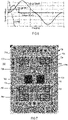
Figure 2 is a current/voltage-time diagram illustrating an exemplary curve of the current through and the voltage across the switching device shortly before and after switching. -
Figure 3 is a voltage-current diagram illustrating exemplary curves of the peak voltage across the snubber capacitor vs. the current provided by the power source for various capacitance values of the snubber capacitor. -
Figure 4 is a side view of is a current/voltage-time diagram illustrating an exemplary curve of the current and voltage across the snubber capacitor shortly before and after switching with aperiodic damping of the snubber circuit. -
Figure 5 is a voltage-current diagram illustrating exemplary curves of the power dissipation of the damping resistance vs. the current provided by the power source for various switching frequencies. -
Figure 6 is a current/voltage-time diagram illustrating an exemplary curve of the current and voltage across the snubber capacitor shortly before and after switching for various capacitance values of the snubber capacitor. -
Figure 7 is a top view of a substrate of an exemplary power semiconductor module that includes at least one snubber circuit. -
Figure 8 is a cross-sectional view of an exemplary snubber circuit including a stack of connection layers, resistive layers and a capacitor with cuboid end caps as terminals. -
Figure 9 is a cross-sectional view of an exemplary snubber circuit including a stack of connection layers, resistive layers and a capacitor with L-shaped terminals. -
Figure 10 is a cross-sectional view of an exemplary snubber circuit including a stack of resistive layers and a capacitor with cuboid end caps as terminals. -
Figure 11 is a cross-sectional view of an exemplary snubber circuit including a stack of resistive layers and a capacitor with L-shaped terminals. -
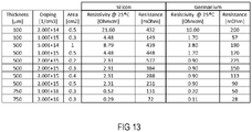
Figure 12 is a cross-sectional view of an exemplary damping resistor including a doped semiconductor layer and two metallic heat capacitances.Figure 13 is table illustrating multiple implementations of such resistive semiconductor layers for different types of semiconductor materials. - Referring to
Figure 1 , an exemplary semiconductor switch having a snubber circuit includes aswitching device 101, e.g., a silicon carbide metal-oxide field-effect transistor or any other appropriate semiconductor switch such as an insulated gate bipolar transistor, metal-oxide field-effect transistor etc., which has a gate terminal G for receiving control signals, a source terminal S that is connected to a first (e.g., negative) terminal of a direct current (DC)power source 102, and a drain terminal D that is connected to a first terminal of aninductive load 103. Theswitching device 101 includes aparasitic chip capacitance 104 between the source terminal S and the drain terminal D, which is consequently connected in parallel to a load path of theswitching device 101, i.e., the path between the source terminal S and the drain terminal D thereof. A second terminal of aninductive load 103 is connected via anparasitic line inductance 105 to a second (e.g., positive) terminal of thepower source 102. A snubber circuit includes adiode 106 that is connected in parallel to theinductive load 103 such that it does not conduct under normal operating conditions, i.e., in the example shown, a cathode ofdiode 106 is connected the first and an anode thereof to the second terminal of theinductive load 103. The snubber circuit further includes an RC element having two series-connected dampingresistors snubber capacitor 108. In this example, the sum of the resistances of the dampingresistors - The snubber circuit described above in connection with
Figure 1 may be adapted in two different ways. In view of one of these ways, to successfully limit overvoltage, thesnubber capacitor 108 is commonly adapted to allow for accumulating all energy from theparasitic line inductance 105 and from thepower source 102 in the time period between the point of switching and the occurrence of a first peak voltage. An accordingly adapted capacitor has a relatively large capacitance and, thus, is large in terms of exterior dimensions. When any parasitic line inductances in between are neglected, the peak voltage across thesnubber capacitor 108 is approximately equal to the voltage across theparasitic chip capacitance 104 of switchingdevice 101, and thus across the load path of theswitching device 101. The not attenuated oscillation frequency f0 of the resonance circuit based on theparasitic line inductance 105 and thesnubber capacitor 108 can be described as:
parasitic line inductance 105 and CSnub represents the capacitance value of thesnubber capacitor 108. At 1/4 of the cycle duration, i.e., at tumax = 1/4·f0, the energy accumulated by thesnubber capacitor 108 is maximum and so is the voltage across thesnubber capacitor 108. The peak voltage USnubmax across thesnubber capacitor 108 can be described as:
snubber capacitor 108, ELS is the energy accumulated in theparasitic line inductance 105, and EDCSource is the energy provided by thepower source 102. -
Figure 2 illustrates the current I in [A] through and the voltage U in [V] across theswitching device 101 over time after switching theswitching device 101 off, provided the damping resistance is sufficient small, i.e., significantly smaller than a resistance for critical damping. Initially, the current I is maximum and drops shortly before the point in time tumax. Inversely, the voltage U raises shortly before the point in time tUmax from approximately zero to maximum at the point in time tUmax with a certain transient curve. - The corresponding peak voltage USnubmax allows for determining the required capacitance value CSnub of the
snubber capacitor 108.Figure 3 depicts for an exemplary inductance value Ls = 20nH of theparasitic line inductance 105 and a voltage UDC provided by thepower source 102 the peak voltage USnubmax over a current IDC provided by thepower source 102, which is equal to a current IL through theparasitic line inductance 105. - In order to damp the oscillation of the resonance circuit, a damping resistance may be inserted, which additionally to the damping of the oscillation also generates a phase shift that shifts the point of time when the peak voltage occurs towards the point of time of switching off. The shift of the peak voltage is apparent from a comparison of
Figure 4 withFigure 2 . A resistance value Radamp of an inserted damping resistance required for aperiodic damping can be determined according to:

parasitic line inductance 105, the product being multiplied by 2 to address on and off switching, according to:
parasitic line inductance 105 in the inserted damping resistance. On the other hand, the damping resistance value may be selected to be as high as possible in order to outweigh frequency dependent parasitic resistances occurring on intermediate connections such as bus bars and, thus, to unload these parasitic resistances. In the example outlined above, such parasitic resistances may amount to between 150mQ and 350mΩ.Figure 5 depicts the power dissipation for an inductance value Ls = 20nH dependent on the current IDC provided by thepower source 102 at different frequencies. - In the other way, the snubber circuit may be adapted to reduce its oscillation. When a higher peak voltage is tolerated, a snubber capacitor with less capacitance and, thus, with smaller dimensions can be employed. However, under certain circumstances the peak voltage across the
snubber capacitor 108 and, correspondingly, across the load path of theswitching device 101, may then be even higher with the snubber circuit than across theswitching device 101 without a snubber circuit. For example, if the capacitance of thesnubber capacitor 108 is so small that 1/4 of the cycle duration of the oscillation is more or less the rise/fall time of the switching device, the switch-off voltage (LS·di/dt) across the load path of theswitching device 101 is superimposed by the oscillation. In the example outlined above, without a snubber circuit an over voltage across the load path of the switching device may exceed 200V and di/dt may be much more than 10A/ns, e.g., up to 40A/ns. - A snubber circuit whose
snubber capacitance 108 has a capacitance of 25nF may generate a voltage of 730V across the load path of theswitching device 101. If the switch device can tolerate voltages higher than the voltages that occur without snubber circuit, the damping resistance can be adapted to generate critical damped oscillations in the snubber circuit.Figure 6 depicts by way of voltage time curve and a current time curve the behavior of the load path current Id of the switching device and the voltage Vd across the load path for a capacitance value of 50nF of the snubber capacitance, a fall time of 50ns, and a damping resistance value Radamp of 1,26Ω. The resulting peak voltage is here 623V.Figure 6 shows for comparison also the curves for the voltage Vd across the load path for a capacitance value of 25nF and 0nF (no snubber). - Because of the higher peak voltage across the load path of the switching device, the power dissipation and, thus, the heat dissipation of the switching device increases compared to the design described above as a first way to adapt the snubber circuit. In turn, the power dissipation and the heat dissipation of the damping resistance then decreases. When increasing the resistance value of the damping resistance, the snubber is less effective and the effects of the
chip capacitor 104 may no longer be negligible, i.e., it may have a significant impact on the oscillation behavior. As can be seen from the above considerations in connection with the two ways of adapting the snubber circuit, the damping resistance value can be selected from a wide range of values, which means de facto that, to implement the damping resistance, also resistors can be used that exhibit broad manufacturing and temperature coefficient variations. - Referring back to the above-described first way for adapting the snubber circuit, as a snubber circuit to be effective requires low parasitic inductances, particularly in the connection paths of the switching device, in the example shown in
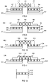
Figure 7 asubstrate 701 of apower semiconductor module 702 with a very compact arrangement is used that, regardless of the compactness, allows for sufficient thermal dissipation, and that is able to include (two)capacitors 703 with larger dimensions due to their higher capacitances. Thesubstrate 701 may be a printed circuit board (PCB), direct copper bonding (DCB) substrate or any other substrate with an electrically insulatingcarrier 704 with an electrically conducting, structured (patterned)layer 705 thereon that interconnects various devices, such as and including switchingdevices 706, arranged on thesubstrate 701. The arrangement used in this example employs a snubber circuit that includes a stapled construction of two resistors and at least one capacitor close to the switching devices 706 (for interconnections seeresistors capacitor 108 inFigure 1 ). For example, thecapacitors 703 have two larger parallel surfaces extending between their terminals and are arranged so that the two larger parallel surfaces are in parallel to at least one larger surface of thesubstrate 701. Thecapacitors 703 are spaced from thesubstrate 701 via resistors (not shown inFigure 7 ), one at each terminal of thecapacitors 703. - Examples for such stacked snubber circuits are illustrated below in connection with
Figures 8-11 . Further, electrically conductive layers or pieces may also be arranged between the capacitor terminals and the resistor(s) and/or between the resistor(s) and the electrically conductive, structured metal layer of the substrate, (e.g., a metal layer pattern). -
Figure 8 depicts an exemplary "stacked"snubber circuit 801 which is attached to two segments of a structuredmetal layer 802. Thesnubber circuit 801 includes electrically conductive, flat first connection layers 803 and 804 (e.g., solder or sheet metal layers) that are each connected to one of the segments of the structuredmetal layer 802. Each of the first connection layers 803 and 804 carries a flatresistive layer resistive layers capacitor 809, which are arranged at two opposite, lateral ends of thecapacitor 809, to the second connection layers 807 and 808. The twoterminals capacitor 809 have the shape of a cuboid end cap and are made from electrically conducting material. - Another exemplary "stacked"
snubber circuit 901 shown inFigure 9 is identical with the snubber circuit shown in Figure 801 with the exception of thecapacitor 809, which is substituted by acapacitor 902. Instead of the two terminals of thecapacitor 809 that have the shape of a cuboid end cap, thecapacitor 902 has, for example, L-shaped terminals which may provide a larger contact area. Alternatively, other shapes such as J-shapes are applicable. J-shapes allow the terminals to extend under the capacitor. -
Figure 10 depicts another exemplary "stacked"snubber circuit 1001 which is attached to two segments of a structuredmetal layer 1002. Thesnubber circuit 1001 includes two, for example flat,resistive layers metal layer 1002, and on an opposite side to twoterminals capacitor 1005, which are arranged at two lateral ends of thecapacitor 1005. The twoterminals capacitor 1005 have the shape of a cuboid end cap made from electrically conducting material. The resistive layers are made from doped semiconductor material. - Another exemplary "stacked"
snubber circuit 1101 shown inFigure 11 is identical with the snubber circuit shown in Figure 1001 with the exception of thecapacitor 1005, which is substituted by acapacitor 1102. Instead of the two terminals of thecapacitor 1005 that have the shape of a cuboid end cap, thecapacitor 1102 has L-shaped terminals which may provide a larger contact area. - According to
Figure 7 , at least one snubber circuit including the capacitor 703 (only a part of the snubber circuit is visible inFigure 7 ) may be disposed in or near the center of thesubstrate 701 and/or in close distance to theswitching devices 706 to allow for a short interconnection distance to ensure low parasitic inductances, particularly in the connection paths between the switching device and the snubber circuit.Figures 8-11 are cross-sections of possible stacked and, thus, very compact snubber circuits applicable as the snubber circuit in the semiconductor module shown inFigure 7 . Resistors, resistances or resistive layers used in the stacked snubber circuit may be made from electrically conductive adhesives, sintered (powder) metal or other resistive material with a suitable resistivity. - In order to achieve a satisfactory peak power behavior of the resistors, resistances or resistive layers, the distribution of the power dissipation within the resistor, resistance or resistive layer may be made homogenous, e.g., by employing conductive material with a homogenous resistivity distribution and a sufficient high overall resistivity. Further, the resistor, resistance or resistive layer may be formed to be relatively flat, i.e., a large sized base area with a small height relative to the substrate. Resistors, resistances or resistive layers with a short distance in the direction of current flow and a large cross section perpendicular to the direction of current flow are not commonly available. The electrically resistive layers may have a height that is equal to or less than 1/5 of the square root of a basic area of the respective electrically resistive layer. For the following considerations it is assumed that the electrically resistive layer has a height that is 1/10 of the square root of a basic area of the respective electrically resistive layer For example, to implement a 300mΩ resistor or restive layer for a height of 1mm and a base area of 1cm2, material having a resistivity with a value ρ = 0.3Ω·100mm2/0.001m = 0.03 Ωm is required. Common resistive materials exhibit typically values that are significantly below 0.03 Ωm. To meet all the requirements outlined above, a semiconductor material such as silicon or silicon carbide (e.g., in the form of a semiconductor layer) with adequate doping may be used. Such material exhibits a high temperature coefficient of resistance, e.g., due to the temperature dependence of the charge carrier mobility, which however has a minor influence in snubber applications as detailed above.
- In order to further improve the peak power behavior of the resistors, resistances or resistive layers, they may be or include a doped
semiconductor layer 1201 that is laminated on its two major surfaces withmetal layers Figure 12 . The metal layers 1202 and 1203 create a type of heat capacitance and may include at least one of copper and aluminum. The connection layers described above in connection withFigures 8 and 10 can be designed to (additionally) have the effect of a heat capacitance. - The semiconductor resistors can be seen as a (semiconductor) material with a homogenous resistivity distribution when neglecting all effects that arise from semiconductor junctions, for example between differently n-doped materials such as N+ (contact), N- (resistive layer) and N+ (further contact), from the edge construction (considering only the active area) of the semiconductor, from the dependency on the mobility of the current density/electric field strength, from the avalanche breakdown field strength, and from the power dissipation. In this case, the resistance R can be described as

Figure 13 is table illustrating multiple implementations of such resistive semiconductor layers for two types of semiconductor materials, e.g., silicon and germanium. - The description of embodiments has been presented for purposes of illustration and description. Suitable modifications and variations to the embodiments may be performed in light of the above description. The described circuits and modules are exemplary in nature, and may include additional elements and/or omit elements.
- As used in this application, an element or step recited in the singular and proceeded with the word "a" or "an" should be understood as not excluding plural of said elements or steps, unless such exclusion is stated. Furthermore, references to "one embodiment" or "one example" of the present disclosure are not intended to be interpreted as excluding the existence of additional embodiments that also incorporate the recited features. The terms "first," "second," and "third," etc. are used merely as labels, and are not intended to impose numerical requirements or a particular positional order on their objects.
- While various embodiments of the invention have been described, it will be apparent to those of ordinary skilled in the art that many more embodiments and implementations are possible within the scope of the invention as defined by the appended claims. In particular, the skilled person will recognize the interchangeability of various features from different embodiments. Although these techniques and systems have been disclosed in the context of certain embodiments and examples, it will be understood that these techniques and systems may be extended beyond the specifically disclosed embodiments to other embodiments and/or uses and obvious modifications thereof.
Claims (14)
- A snubber circuit comprising:a snubber substrate (701) comprising an electrically insulating carrier (704) and an electrically conducting structured metal layer (705, 802, 1002) applied thereon, the electrically conducting structured metal layer of the snubber substrate (701) including two segments;two electrically resistive layers (805, 806, 1003, 1004) having two opposing ends, each resistive layer (805, 806, 1003, 1004) being carried by and electrically connected on one end to one of the two segments of the electrically conducting structured metal layer (705, 802, 1002) of the snubber substrate (701); anda capacitor (809, 902, 105, 1102) disposed on the electrically resistive layers (805, 806, 1003, 1004) and having two terminals (810, 811, 903, 904, 1006, 1007, 1103) at two opposite, lateral ends, each terminal (810, 811, 903, 904, 1006, 1007, 1103) being electrically connected to another end of one of the electrically resistive layers (805, 806, 1003, 1004), characterized in that each of the two electrically resistive layers (805, 806, 1003, 1004) comprises or consists of doped semiconductor material.
- The snubber circuit of claim 1, wherein at least one of:first electrically conductive interconnecting layers (803, 804) are disposed between the two electrically resistive layers (805, 806) and the two segments of the electrically conducting structured metal layer (802) of the snubber substrate (701); andsecond electrically conductive interconnecting layers (807, 808) are disposed between the two electrically resistive layers (805, 806) (805, 806) and the two terminals (810, 811, 903, 904) of the capacitor (809, 902).
- The snubber circuit of claim 2, wherein at least one of the first electrically conductive interconnecting layers (803, 804) and the second electrically conductive interconnecting layers (807, 808) is configured to have the effect of a heat capacitance.
- The snubber circuit of any of claims 1-3, wherein the two electrically resistive layers (805, 806, 1003, 1004) comprise a resistivity of more than 0.03 Ωm.
- The snubber circuit of any of claims 1-4, wherein the two electrically resistive layers (805, 806, 1003, 1004) have a height that is equal to or less than 1/5 of the square root of a basic area of the respective electrically resistive layer (805, 806, 1003, 1004).
- The snubber circuit of claim 4 or 5, wherein the electrically resistive layers (805, 806, 1003, 1004) comprise material with a homogenous resistivity distribution.
- The snubber circuit of any of claims 1-6, wherein the terminals (810, 811, 903, 904) of the capacitor (809, 902, 105, 1102) are arranged at the lateral ends of the capacitor (809, 902, 105, 1102) and have a shape of a cuboid end cap.
- The snubber circuit of any of claims 1-6, wherein the terminals (810, 811, 903, 904) of the capacitor (809, 902, 105, 1102) are arranged at the lateral ends of the capacitor (809, 902, 105, 1102) and have an L-shape.
- A power semiconductor module comprising:a module substrate (701) comprising an electrically insulating carrier (704) and an electrically conducting structured metal layer (705) applied thereon, the electrically conducting structured metal layer (705) including multiple segments;at least one semiconductor switching device (706) disposed on the module substrate (701) and electrically connected to the electrically conducting structured metal layer (705); andat least one snubber circuit according to any of claims 1-8 disposed on the module substrate (701) and connected via the electrically conducting structured layer of the module substrate (701) to the at least one semiconductor switching device (706).
- The power semiconductor module of claim 9, wherein the at least one snubber circuit is disposed in close proximity to the at least one semiconductor switching device (706).
- The power semiconductor module of claim 9 or 10, wherein the snubber substrate (701) is part of the module substrate (701).
- The power semiconductor module of any of claims 9-11, wherein the at least one semiconductor switching device (706) is a silicon-carbide metal-oxide field-effect transistor.
- The power semiconductor module of any of claims 9-12, wherein the snubber circuit further comprises a snubber diode (106).
- The power semiconductor module of any of claims 9-13, wherein the at least one snubber circuit is disposed in the center of the module substrate (701).
Priority Applications (3)
| Application Number | Priority Date | Filing Date | Title |
|---|---|---|---|
| EP19184691.4A EP3761492B1 (en) | 2019-07-05 | 2019-07-05 | Snubber circuit and power semiconductor module with snubber circuit |
| CN202010606317.5A CN112188730A (en) | 2019-07-05 | 2020-06-29 | Snubber circuit and power semiconductor module having the same |
| US16/919,518 US11631974B2 (en) | 2019-07-05 | 2020-07-02 | Snubber circuit and power semiconductor module with snubber circuit |
Applications Claiming Priority (1)
| Application Number | Priority Date | Filing Date | Title |
|---|---|---|---|
| EP19184691.4A EP3761492B1 (en) | 2019-07-05 | 2019-07-05 | Snubber circuit and power semiconductor module with snubber circuit |
Publications (2)
| Publication Number | Publication Date |
|---|---|
| EP3761492A1 EP3761492A1 (en) | 2021-01-06 |
| EP3761492B1 true EP3761492B1 (en) | 2023-01-04 |
Family
ID=67211529
Family Applications (1)
| Application Number | Title | Priority Date | Filing Date |
|---|---|---|---|
| EP19184691.4A Active EP3761492B1 (en) | 2019-07-05 | 2019-07-05 | Snubber circuit and power semiconductor module with snubber circuit |
Country Status (3)
| Country | Link |
|---|---|
| US (1) | US11631974B2 (en) |
| EP (1) | EP3761492B1 (en) |
| CN (1) | CN112188730A (en) |
Families Citing this family (2)
| Publication number | Priority date | Publication date | Assignee | Title |
|---|---|---|---|---|
| US11711025B2 (en) * | 2018-02-20 | 2023-07-25 | Mitsubishi Electric Corporation | Power semiconductor module and power conversion apparatus including the same |
| DE112019001683T5 (en) * | 2018-06-15 | 2021-03-11 | Murata Manufacturing Co., Ltd. | RC SNUBBER LINK |
Citations (1)
| Publication number | Priority date | Publication date | Assignee | Title |
|---|---|---|---|---|
| JP2010123728A (en) * | 2008-11-19 | 2010-06-03 | Nec Tokin Corp | Solid electrolytic capacitor |
Family Cites Families (30)
| Publication number | Priority date | Publication date | Assignee | Title |
|---|---|---|---|---|
| US4916576A (en) * | 1989-02-27 | 1990-04-10 | Fmtt, Inc. | Matrix capacitor |
| US5006822A (en) * | 1990-01-03 | 1991-04-09 | Prabhakara Reddy | Hybrid RF coupling device with integrated capacitors and resistors |
| EP1492220A3 (en) * | 1991-09-20 | 2005-03-09 | Hitachi, Ltd. | IGBT-module |
| JP3226246B2 (en) * | 1994-03-11 | 2001-11-05 | 株式会社東芝 | High voltage self-excited converter for grid interconnection |
| JP3263317B2 (en) * | 1996-06-18 | 2002-03-04 | 株式会社東芝 | Switching module and power converter using the module |
| US7430128B2 (en) * | 2004-10-18 | 2008-09-30 | E.I. Du Pont De Nemours And Company | Capacitive/resistive devices, organic dielectric laminates and printed wiring boards incorporating such devices, and methods of making thereof |
| DE102006017487A1 (en) * | 2006-04-13 | 2007-10-18 | Fraunhofer-Gesellschaft zur Förderung der angewandten Forschung e.V. | Semiconductor-based integrated circuit component for switching discharge, voltage limitation or vibration damping |
| JP4803451B2 (en) * | 2006-12-26 | 2011-10-26 | Tdk株式会社 | Electronic component and its mounting structure |
| US20080233704A1 (en) * | 2007-03-23 | 2008-09-25 | Honeywell International Inc. | Integrated Resistor Capacitor Structure |
| JP5218541B2 (en) * | 2010-12-14 | 2013-06-26 | 株式会社デンソー | Switching module |
| JP5447603B2 (en) * | 2011-08-27 | 2014-03-19 | 株式会社デンソー | Power converter |
| JP5488638B2 (en) * | 2012-04-11 | 2014-05-14 | 株式会社デンソー | Power converter |
| JP5860784B2 (en) * | 2012-09-10 | 2016-02-16 | 日立オートモティブシステムズ株式会社 | Power semiconductor module |
| JP5737272B2 (en) * | 2012-11-14 | 2015-06-17 | トヨタ自動車株式会社 | Semiconductor device |
| JP5558645B1 (en) * | 2013-10-02 | 2014-07-23 | 三菱電機株式会社 | CR snubber circuit |
| JP6196931B2 (en) * | 2014-04-23 | 2017-09-13 | 株式会社豊田中央研究所 | Module with built-in snubber circuit |
| US9601920B2 (en) * | 2014-07-10 | 2017-03-21 | Infineon Technologies Ag | Transient voltage protection circuits and devices |
| JP6683621B2 (en) * | 2014-10-30 | 2020-04-22 | ローム株式会社 | Power modules and power circuits |
| US10680518B2 (en) * | 2015-03-16 | 2020-06-09 | Cree, Inc. | High speed, efficient SiC power module |
| FR3044184B1 (en) * | 2015-11-23 | 2018-03-23 | IFP Energies Nouvelles | MODULAR SYSTEM FOR CONVERTING CONTINUOUS ELECTRIC POWER IN THREE-PHASE ELECTRIC POWER |
| KR102494751B1 (en) * | 2015-12-11 | 2023-02-02 | 삼성전자 주식회사 | variable resistance memory device and method of manufacturing the same |
| EP3249686A1 (en) * | 2016-05-24 | 2017-11-29 | Mitsubishi Electric R&D Centre Europe B.V. | A power module |
| WO2018080540A1 (en) * | 2016-10-31 | 2018-05-03 | Han Weishan | Applying e-field antennas to resistivity logging tools |
| US10593664B2 (en) * | 2016-12-27 | 2020-03-17 | Infineon Technologies Americas Corp. | Controlled resistance integrated snubber for power switching device |
| US11355477B2 (en) * | 2017-02-06 | 2022-06-07 | Mitsubishi Electric Corporation | Power semiconductor module and power conversion device |
| US10530270B2 (en) * | 2017-12-01 | 2020-01-07 | Qatar University | Modular isolated half-bridge based capacitor-tapped multi-module converter with inherent DC fault segregation capability |
| WO2019244658A1 (en) * | 2018-06-23 | 2019-12-26 | 株式会社村田製作所 | Electronic module and switching power supply |
| JP6939740B2 (en) * | 2018-08-24 | 2021-09-22 | 三菱電機株式会社 | Semiconductor module |
| JP7038632B2 (en) * | 2018-09-12 | 2022-03-18 | 三菱電機株式会社 | Semiconductor devices and methods for manufacturing semiconductor devices |
| JP7358921B2 (en) * | 2019-11-08 | 2023-10-11 | 富士電機株式会社 | Semiconductor module and semiconductor module manufacturing method |
-
2019
- 2019-07-05 EP EP19184691.4A patent/EP3761492B1/en active Active
-
2020
- 2020-06-29 CN CN202010606317.5A patent/CN112188730A/en active Pending
- 2020-07-02 US US16/919,518 patent/US11631974B2/en active Active
Patent Citations (1)
| Publication number | Priority date | Publication date | Assignee | Title |
|---|---|---|---|---|
| JP2010123728A (en) * | 2008-11-19 | 2010-06-03 | Nec Tokin Corp | Solid electrolytic capacitor |
Also Published As
| Publication number | Publication date |
|---|---|
| US20210006062A1 (en) | 2021-01-07 |
| US11631974B2 (en) | 2023-04-18 |
| CN112188730A (en) | 2021-01-05 |
| EP3761492A1 (en) | 2021-01-06 |
Similar Documents
| Publication | Publication Date | Title |
|---|---|---|
| US7738226B2 (en) | Integrated snubber device on a semiconductor basis for switching load reduction, voltage limitation and/or oscillation attenuation | |
| JP6245365B2 (en) | Half-bridge power semiconductor module and manufacturing method thereof | |
| CN103782380B (en) | semiconductor module | |
| EP2549650A1 (en) | Method for driving IGBT | |
| JP2014060914A (en) | Capacitor bank, laminated bus bar, and power supply apparatus | |
| JP5277579B2 (en) | Semiconductor device | |
| US11631974B2 (en) | Snubber circuit and power semiconductor module with snubber circuit | |
| US10530361B2 (en) | Electrical circuit arrangement with an active discharge circuit | |
| US7339776B1 (en) | Silicon carbide diode voltage limiter | |
| Konrad et al. | New demands on DC link power capacitors | |
| US11303201B2 (en) | CR snubber element | |
| TWI782953B (en) | Hybrid overvoltage protection device and assembly | |
| US6438002B2 (en) | Active snubber circuit with controllable DV/DT | |
| JP4773172B2 (en) | Voltage detection method for power switching element and power conversion device using the same | |
| JP2005251839A (en) | Insulating substrate of power semiconductor module | |
| EP3355456A1 (en) | A protection arrangement for an mmc-hvdc sub-module | |
| TW201842730A (en) | High power amplifier circuit with protective feedback circuit | |
| US20170125394A1 (en) | Wide Bandgap Junction Barrier Schottky Diode With Silicon Bypass | |
| CN109936114B (en) | Semiconductor assembly and control method thereof | |
| JP5557571B2 (en) | Diode module | |
| JP2020140996A (en) | Semiconductor device | |
| JP6973954B2 (en) | DC cutoff device | |
| Peri et al. | Design and performance evaluation of a general purpose device characterization setup | |
| JP2007336637A (en) | Power converter | |
| JP5899947B2 (en) | Power semiconductor module and power conversion device |
Legal Events
| Date | Code | Title | Description |
|---|---|---|---|
| PUAI | Public reference made under article 153(3) epc to a published international application that has entered the european phase |
Free format text: ORIGINAL CODE: 0009012 |
|
| STAA | Information on the status of an ep patent application or granted ep patent |
Free format text: STATUS: THE APPLICATION HAS BEEN PUBLISHED |
|
| AK | Designated contracting states |
Kind code of ref document: A1 Designated state(s): AL AT BE BG CH CY CZ DE DK EE ES FI FR GB GR HR HU IE IS IT LI LT LU LV MC MK MT NL NO PL PT RO RS SE SI SK SM TR |
|
| AX | Request for extension of the european patent |
Extension state: BA ME |
|
| STAA | Information on the status of an ep patent application or granted ep patent |
Free format text: STATUS: REQUEST FOR EXAMINATION WAS MADE |
|
| STAA | Information on the status of an ep patent application or granted ep patent |
Free format text: STATUS: EXAMINATION IS IN PROGRESS |
|
| 17P | Request for examination filed |
Effective date: 20210701 |
|
| RBV | Designated contracting states (corrected) |
Designated state(s): AL AT BE BG CH CY CZ DE DK EE ES FI FR GB GR HR HU IE IS IT LI LT LU LV MC MK MT NL NO PL PT RO RS SE SI SK SM TR |
|
| 17Q | First examination report despatched |
Effective date: 20210809 |
|
| GRAP | Despatch of communication of intention to grant a patent |
Free format text: ORIGINAL CODE: EPIDOSNIGR1 |
|
| STAA | Information on the status of an ep patent application or granted ep patent |
Free format text: STATUS: GRANT OF PATENT IS INTENDED |
|
| INTG | Intention to grant announced |
Effective date: 20220908 |
|
| GRAS | Grant fee paid |
Free format text: ORIGINAL CODE: EPIDOSNIGR3 |
|
| GRAA | (expected) grant |
Free format text: ORIGINAL CODE: 0009210 |
|
| STAA | Information on the status of an ep patent application or granted ep patent |
Free format text: STATUS: THE PATENT HAS BEEN GRANTED |
|
| AK | Designated contracting states |
Kind code of ref document: B1 Designated state(s): AL AT BE BG CH CY CZ DE DK EE ES FI FR GB GR HR HU IE IS IT LI LT LU LV MC MK MT NL NO PL PT RO RS SE SI SK SM TR |
|
| REG | Reference to a national code |
Ref country code: GB Ref legal event code: FG4D |
|
| REG | Reference to a national code |
Ref country code: CH Ref legal event code: EP |
|
| REG | Reference to a national code |
Ref country code: AT Ref legal event code: REF Ref document number: 1542645 Country of ref document: AT Kind code of ref document: T Effective date: 20230115 |
|
| REG | Reference to a national code |
Ref country code: DE Ref legal event code: R096 Ref document number: 602019023876 Country of ref document: DE |
|
| REG | Reference to a national code |
Ref country code: IE Ref legal event code: FG4D |
|
| REG | Reference to a national code |
Ref country code: LT Ref legal event code: MG9D |
|
| REG | Reference to a national code |
Ref country code: NL Ref legal event code: MP Effective date: 20230104 |
|
| REG | Reference to a national code |
Ref country code: AT Ref legal event code: MK05 Ref document number: 1542645 Country of ref document: AT Kind code of ref document: T Effective date: 20230104 |
|
| PG25 | Lapsed in a contracting state [announced via postgrant information from national office to epo] |
Ref country code: NL Free format text: LAPSE BECAUSE OF FAILURE TO SUBMIT A TRANSLATION OF THE DESCRIPTION OR TO PAY THE FEE WITHIN THE PRESCRIBED TIME-LIMIT Effective date: 20230104 |
|
| P01 | Opt-out of the competence of the unified patent court (upc) registered |
Effective date: 20230528 |
|
| PG25 | Lapsed in a contracting state [announced via postgrant information from national office to epo] |
Ref country code: RS Free format text: LAPSE BECAUSE OF FAILURE TO SUBMIT A TRANSLATION OF THE DESCRIPTION OR TO PAY THE FEE WITHIN THE PRESCRIBED TIME-LIMIT Effective date: 20230104 Ref country code: PT Free format text: LAPSE BECAUSE OF FAILURE TO SUBMIT A TRANSLATION OF THE DESCRIPTION OR TO PAY THE FEE WITHIN THE PRESCRIBED TIME-LIMIT Effective date: 20230504 Ref country code: NO Free format text: LAPSE BECAUSE OF FAILURE TO SUBMIT A TRANSLATION OF THE DESCRIPTION OR TO PAY THE FEE WITHIN THE PRESCRIBED TIME-LIMIT Effective date: 20230404 Ref country code: LV Free format text: LAPSE BECAUSE OF FAILURE TO SUBMIT A TRANSLATION OF THE DESCRIPTION OR TO PAY THE FEE WITHIN THE PRESCRIBED TIME-LIMIT Effective date: 20230104 Ref country code: LT Free format text: LAPSE BECAUSE OF FAILURE TO SUBMIT A TRANSLATION OF THE DESCRIPTION OR TO PAY THE FEE WITHIN THE PRESCRIBED TIME-LIMIT Effective date: 20230104 Ref country code: HR Free format text: LAPSE BECAUSE OF FAILURE TO SUBMIT A TRANSLATION OF THE DESCRIPTION OR TO PAY THE FEE WITHIN THE PRESCRIBED TIME-LIMIT Effective date: 20230104 Ref country code: ES Free format text: LAPSE BECAUSE OF FAILURE TO SUBMIT A TRANSLATION OF THE DESCRIPTION OR TO PAY THE FEE WITHIN THE PRESCRIBED TIME-LIMIT Effective date: 20230104 Ref country code: AT Free format text: LAPSE BECAUSE OF FAILURE TO SUBMIT A TRANSLATION OF THE DESCRIPTION OR TO PAY THE FEE WITHIN THE PRESCRIBED TIME-LIMIT Effective date: 20230104 |
|
| PG25 | Lapsed in a contracting state [announced via postgrant information from national office to epo] |
Ref country code: SE Free format text: LAPSE BECAUSE OF FAILURE TO SUBMIT A TRANSLATION OF THE DESCRIPTION OR TO PAY THE FEE WITHIN THE PRESCRIBED TIME-LIMIT Effective date: 20230104 Ref country code: PL Free format text: LAPSE BECAUSE OF FAILURE TO SUBMIT A TRANSLATION OF THE DESCRIPTION OR TO PAY THE FEE WITHIN THE PRESCRIBED TIME-LIMIT Effective date: 20230104 Ref country code: IS Free format text: LAPSE BECAUSE OF FAILURE TO SUBMIT A TRANSLATION OF THE DESCRIPTION OR TO PAY THE FEE WITHIN THE PRESCRIBED TIME-LIMIT Effective date: 20230504 Ref country code: GR Free format text: LAPSE BECAUSE OF FAILURE TO SUBMIT A TRANSLATION OF THE DESCRIPTION OR TO PAY THE FEE WITHIN THE PRESCRIBED TIME-LIMIT Effective date: 20230405 Ref country code: FI Free format text: LAPSE BECAUSE OF FAILURE TO SUBMIT A TRANSLATION OF THE DESCRIPTION OR TO PAY THE FEE WITHIN THE PRESCRIBED TIME-LIMIT Effective date: 20230104 |
|
| REG | Reference to a national code |
Ref country code: DE Ref legal event code: R097 Ref document number: 602019023876 Country of ref document: DE |
|
| PG25 | Lapsed in a contracting state [announced via postgrant information from national office to epo] |
Ref country code: SM Free format text: LAPSE BECAUSE OF FAILURE TO SUBMIT A TRANSLATION OF THE DESCRIPTION OR TO PAY THE FEE WITHIN THE PRESCRIBED TIME-LIMIT Effective date: 20230104 Ref country code: RO Free format text: LAPSE BECAUSE OF FAILURE TO SUBMIT A TRANSLATION OF THE DESCRIPTION OR TO PAY THE FEE WITHIN THE PRESCRIBED TIME-LIMIT Effective date: 20230104 Ref country code: EE Free format text: LAPSE BECAUSE OF FAILURE TO SUBMIT A TRANSLATION OF THE DESCRIPTION OR TO PAY THE FEE WITHIN THE PRESCRIBED TIME-LIMIT Effective date: 20230104 Ref country code: DK Free format text: LAPSE BECAUSE OF FAILURE TO SUBMIT A TRANSLATION OF THE DESCRIPTION OR TO PAY THE FEE WITHIN THE PRESCRIBED TIME-LIMIT Effective date: 20230104 Ref country code: CZ Free format text: LAPSE BECAUSE OF FAILURE TO SUBMIT A TRANSLATION OF THE DESCRIPTION OR TO PAY THE FEE WITHIN THE PRESCRIBED TIME-LIMIT Effective date: 20230104 |
|
| PLBE | No opposition filed within time limit |
Free format text: ORIGINAL CODE: 0009261 |
|
| STAA | Information on the status of an ep patent application or granted ep patent |
Free format text: STATUS: NO OPPOSITION FILED WITHIN TIME LIMIT |
|
| PG25 | Lapsed in a contracting state [announced via postgrant information from national office to epo] |
Ref country code: SK Free format text: LAPSE BECAUSE OF FAILURE TO SUBMIT A TRANSLATION OF THE DESCRIPTION OR TO PAY THE FEE WITHIN THE PRESCRIBED TIME-LIMIT Effective date: 20230104 |
|
| PGFP | Annual fee paid to national office [announced via postgrant information from national office to epo] |
Ref country code: DE Payment date: 20230922 Year of fee payment: 5 |
|
| 26N | No opposition filed |
Effective date: 20231005 |
|
| PG25 | Lapsed in a contracting state [announced via postgrant information from national office to epo] |
Ref country code: SI Free format text: LAPSE BECAUSE OF FAILURE TO SUBMIT A TRANSLATION OF THE DESCRIPTION OR TO PAY THE FEE WITHIN THE PRESCRIBED TIME-LIMIT Effective date: 20230104 |
|
| PG25 | Lapsed in a contracting state [announced via postgrant information from national office to epo] |
Ref country code: MC Free format text: LAPSE BECAUSE OF FAILURE TO SUBMIT A TRANSLATION OF THE DESCRIPTION OR TO PAY THE FEE WITHIN THE PRESCRIBED TIME-LIMIT Effective date: 20230104 |
|
| PG25 | Lapsed in a contracting state [announced via postgrant information from national office to epo] |
Ref country code: MC Free format text: LAPSE BECAUSE OF FAILURE TO SUBMIT A TRANSLATION OF THE DESCRIPTION OR TO PAY THE FEE WITHIN THE PRESCRIBED TIME-LIMIT Effective date: 20230104 |
|
| REG | Reference to a national code |
Ref country code: CH Ref legal event code: PL |
|
| REG | Reference to a national code |
Ref country code: BE Ref legal event code: MM Effective date: 20230731 |
|
| PG25 | Lapsed in a contracting state [announced via postgrant information from national office to epo] |
Ref country code: LU Free format text: LAPSE BECAUSE OF NON-PAYMENT OF DUE FEES Effective date: 20230705 |
|
| GBPC | Gb: european patent ceased through non-payment of renewal fee |
Effective date: 20230705 |
|
| PG25 | Lapsed in a contracting state [announced via postgrant information from national office to epo] |
Ref country code: LU Free format text: LAPSE BECAUSE OF NON-PAYMENT OF DUE FEES Effective date: 20230705 |
|
| PG25 | Lapsed in a contracting state [announced via postgrant information from national office to epo] |
Ref country code: GB Free format text: LAPSE BECAUSE OF NON-PAYMENT OF DUE FEES Effective date: 20230705 Ref country code: CH Free format text: LAPSE BECAUSE OF NON-PAYMENT OF DUE FEES Effective date: 20230731 |