EP3672078A1 - Method for controlling semiconductors - Google Patents
Method for controlling semiconductors Download PDFInfo
- Publication number
- EP3672078A1 EP3672078A1 EP18213350.4A EP18213350A EP3672078A1 EP 3672078 A1 EP3672078 A1 EP 3672078A1 EP 18213350 A EP18213350 A EP 18213350A EP 3672078 A1 EP3672078 A1 EP 3672078A1
- Authority
- EP
- European Patent Office
- Prior art keywords
- semiconductors
- signal line
- control unit
- signal
- converter
- Prior art date
- Legal status (The legal status is an assumption and is not a legal conclusion. Google has not performed a legal analysis and makes no representation as to the accuracy of the status listed.)
- Withdrawn
Links
- 239000004065 semiconductor Substances 0.000 title claims abstract description 110
- 238000000034 method Methods 0.000 title claims abstract description 13
- 230000003287 optical effect Effects 0.000 claims description 5
- 230000005540 biological transmission Effects 0.000 abstract description 7
- 230000008054 signal transmission Effects 0.000 abstract description 7
- 238000009434 installation Methods 0.000 abstract description 3
- 230000001681 protective effect Effects 0.000 description 12
- 230000006378 damage Effects 0.000 description 4
- 230000035484 reaction time Effects 0.000 description 3
- RYGMFSIKBFXOCR-UHFFFAOYSA-N Copper Chemical compound [Cu] RYGMFSIKBFXOCR-UHFFFAOYSA-N 0.000 description 2
- 229910052802 copper Inorganic materials 0.000 description 2
- 239000010949 copper Substances 0.000 description 2
- 230000000694 effects Effects 0.000 description 2
- 239000000835 fiber Substances 0.000 description 2
- 238000004519 manufacturing process Methods 0.000 description 2
- 208000027418 Wounds and injury Diseases 0.000 description 1
- 230000001133 acceleration Effects 0.000 description 1
- 230000015572 biosynthetic process Effects 0.000 description 1
- 230000001419 dependent effect Effects 0.000 description 1
- 238000001514 detection method Methods 0.000 description 1
- 238000011156 evaluation Methods 0.000 description 1
- 208000014674 injury Diseases 0.000 description 1
- 238000002955 isolation Methods 0.000 description 1
- 239000013307 optical fiber Substances 0.000 description 1
- 230000002123 temporal effect Effects 0.000 description 1
Images


Classifications
-
- H—ELECTRICITY
- H03—ELECTRONIC CIRCUITRY
- H03K—PULSE TECHNIQUE
- H03K17/00—Electronic switching or gating, i.e. not by contact-making and –breaking
- H03K17/08—Modifications for protecting switching circuit against overcurrent or overvoltage
- H03K17/081—Modifications for protecting switching circuit against overcurrent or overvoltage without feedback from the output circuit to the control circuit
- H03K17/0812—Modifications for protecting switching circuit against overcurrent or overvoltage without feedback from the output circuit to the control circuit by measures taken in the control circuit
-
- H—ELECTRICITY
- H02—GENERATION; CONVERSION OR DISTRIBUTION OF ELECTRIC POWER
- H02M—APPARATUS FOR CONVERSION BETWEEN AC AND AC, BETWEEN AC AND DC, OR BETWEEN DC AND DC, AND FOR USE WITH MAINS OR SIMILAR POWER SUPPLY SYSTEMS; CONVERSION OF DC OR AC INPUT POWER INTO SURGE OUTPUT POWER; CONTROL OR REGULATION THEREOF
- H02M1/00—Details of apparatus for conversion
- H02M1/08—Circuits specially adapted for the generation of control voltages for semiconductor devices incorporated in static converters
- H02M1/088—Circuits specially adapted for the generation of control voltages for semiconductor devices incorporated in static converters for the simultaneous control of series or parallel connected semiconductor devices
-
- B—PERFORMING OPERATIONS; TRANSPORTING
- B60—VEHICLES IN GENERAL
- B60R—VEHICLES, VEHICLE FITTINGS, OR VEHICLE PARTS, NOT OTHERWISE PROVIDED FOR
- B60R16/00—Electric or fluid circuits specially adapted for vehicles and not otherwise provided for; Arrangement of elements of electric or fluid circuits specially adapted for vehicles and not otherwise provided for
- B60R16/02—Electric or fluid circuits specially adapted for vehicles and not otherwise provided for; Arrangement of elements of electric or fluid circuits specially adapted for vehicles and not otherwise provided for electric constitutive elements
- B60R16/03—Electric or fluid circuits specially adapted for vehicles and not otherwise provided for; Arrangement of elements of electric or fluid circuits specially adapted for vehicles and not otherwise provided for electric constitutive elements for supply of electrical power to vehicle subsystems or for
-
- H—ELECTRICITY
- H02—GENERATION; CONVERSION OR DISTRIBUTION OF ELECTRIC POWER
- H02M—APPARATUS FOR CONVERSION BETWEEN AC AND AC, BETWEEN AC AND DC, OR BETWEEN DC AND DC, AND FOR USE WITH MAINS OR SIMILAR POWER SUPPLY SYSTEMS; CONVERSION OF DC OR AC INPUT POWER INTO SURGE OUTPUT POWER; CONTROL OR REGULATION THEREOF
- H02M1/00—Details of apparatus for conversion
- H02M1/08—Circuits specially adapted for the generation of control voltages for semiconductor devices incorporated in static converters
- H02M1/088—Circuits specially adapted for the generation of control voltages for semiconductor devices incorporated in static converters for the simultaneous control of series or parallel connected semiconductor devices
- H02M1/092—Circuits specially adapted for the generation of control voltages for semiconductor devices incorporated in static converters for the simultaneous control of series or parallel connected semiconductor devices the control signals being transmitted optically
-
- H—ELECTRICITY
- H02—GENERATION; CONVERSION OR DISTRIBUTION OF ELECTRIC POWER
- H02M—APPARATUS FOR CONVERSION BETWEEN AC AND AC, BETWEEN AC AND DC, OR BETWEEN DC AND DC, AND FOR USE WITH MAINS OR SIMILAR POWER SUPPLY SYSTEMS; CONVERSION OF DC OR AC INPUT POWER INTO SURGE OUTPUT POWER; CONTROL OR REGULATION THEREOF
- H02M5/00—Conversion of ac power input into ac power output, e.g. for change of voltage, for change of frequency, for change of number of phases
- H02M5/40—Conversion of ac power input into ac power output, e.g. for change of voltage, for change of frequency, for change of number of phases with intermediate conversion into dc
- H02M5/42—Conversion of ac power input into ac power output, e.g. for change of voltage, for change of frequency, for change of number of phases with intermediate conversion into dc by static converters
- H02M5/44—Conversion of ac power input into ac power output, e.g. for change of voltage, for change of frequency, for change of number of phases with intermediate conversion into dc by static converters using discharge tubes or semiconductor devices to convert the intermediate dc into ac
- H02M5/453—Conversion of ac power input into ac power output, e.g. for change of voltage, for change of frequency, for change of number of phases with intermediate conversion into dc by static converters using discharge tubes or semiconductor devices to convert the intermediate dc into ac using devices of a triode or transistor type requiring continuous application of a control signal
- H02M5/458—Conversion of ac power input into ac power output, e.g. for change of voltage, for change of frequency, for change of number of phases with intermediate conversion into dc by static converters using discharge tubes or semiconductor devices to convert the intermediate dc into ac using devices of a triode or transistor type requiring continuous application of a control signal using semiconductor devices only
- H02M5/4585—Conversion of ac power input into ac power output, e.g. for change of voltage, for change of frequency, for change of number of phases with intermediate conversion into dc by static converters using discharge tubes or semiconductor devices to convert the intermediate dc into ac using devices of a triode or transistor type requiring continuous application of a control signal using semiconductor devices only having a rectifier with controlled elements
-
- H—ELECTRICITY
- H03—ELECTRONIC CIRCUITRY
- H03K—PULSE TECHNIQUE
- H03K17/00—Electronic switching or gating, i.e. not by contact-making and –breaking
- H03K17/04—Modifications for accelerating switching
- H03K17/041—Modifications for accelerating switching without feedback from the output circuit to the control circuit
- H03K17/0412—Modifications for accelerating switching without feedback from the output circuit to the control circuit by measures taken in the control circuit
-
- Y—GENERAL TAGGING OF NEW TECHNOLOGICAL DEVELOPMENTS; GENERAL TAGGING OF CROSS-SECTIONAL TECHNOLOGIES SPANNING OVER SEVERAL SECTIONS OF THE IPC; TECHNICAL SUBJECTS COVERED BY FORMER USPC CROSS-REFERENCE ART COLLECTIONS [XRACs] AND DIGESTS
- Y02—TECHNOLOGIES OR APPLICATIONS FOR MITIGATION OR ADAPTATION AGAINST CLIMATE CHANGE
- Y02E—REDUCTION OF GREENHOUSE GAS [GHG] EMISSIONS, RELATED TO ENERGY GENERATION, TRANSMISSION OR DISTRIBUTION
- Y02E10/00—Energy generation through renewable energy sources
- Y02E10/70—Wind energy
- Y02E10/72—Wind turbines with rotation axis in wind direction
Definitions
- the invention relates to a method for controlling a large number of semiconductors by means of a control unit, a signal line being arranged between the control unit and the semiconductors, a protocol for controlling the semiconductors being transmitted via the signal line. Furthermore, the invention relates to a semiconductor circuit with a multiplicity of semiconductors, each with a driver circuit and a control unit, a signal line being arranged between the control unit and the semiconductors, a protocol for controlling the semiconductors being transferable via the signal line. The invention further relates to a converter with such a semiconductor circuit. The invention further relates to a vehicle with such a converter and to a wind energy installation with such a converter.
- a switch is made between a control system and the semiconductors from a parallel control method to a serial control method. While the parallel control method requires a single control line for each semiconductor to be controlled, this information is bundled on only one line in the serial control method and transmitted using a protocol, also known as a telegram.
- the semiconductors each have a driver circuit which transmits the signal relevant to them, in particular with regard to the control, i.e. Switching on or off, evaluated and implemented on the semiconductor.
- the invention has for its object to improve the transmission of signals from the control unit to the converter with regard to the transmission security.
- This object is achieved by a method for controlling a large number of semiconductors by means of a control unit in that a signal line is arranged between the control unit and the semiconductors, a protocol for controlling the semiconductors being transmitted via the signal line, a live signal additionally being transmitted via the signal line is transmitted, the semiconductors being switched off in the absence of the live signal. Furthermore, this object is achieved by a semiconductor circuit comprising a plurality of semiconductors, each with a driver circuit and a control unit, in that a signal line is arranged between the control unit and the semiconductors, a protocol for controlling the semiconductors being transferable via the signal line, the signal line can additionally transmit a live signal, the semiconductors being able to be switched off by means of the respective driver circuit if the live signal is absent.
- This object is further achieved by a power converter with such a semiconductor circuit in that the semiconductors or at least some of the semiconductors are arranged in a bridge circuit. Furthermore, this object is achieved by a vehicle with such a converter and by a wind energy installation with such a converter.
- the invention is based on the finding that the transmission security can be improved if a failure or a disturbance in the signal transmission of the signal transmission is detected reliably and quickly.
- a fault is usually recognized when the protocol or telegram is evaluated.
- the protocol can be constructed in such a way that it recognizes errors in the transmission.
- An example of such a telegram is a CRC coding.
- the use of telegrams results in delay times for the formation of the switching information in the semiconductor circuit or in the converter, which are also necessary Protective shutdowns (detected and executed by the control unit) act. As a result, a sufficient protection concept for the converter is no longer guaranteed, since protective switch-off times between one and two telegram lengths result.
- the error detection time or the requirement for the semiconductor to be switched off by the control unit as a protective intervention is thus in the order of 5 ⁇ s to 10 ⁇ s. During this time, currents can already occur in the semiconductor circuit or in the converter, which lead to damage or destruction of the semiconductor or converter.
- a live signal is therefore superimposed on the serial telegrams for controlling the semiconductors on the same signal line by the control unit. This is constantly monitored for absence on the driver circuit of the semiconductor. If it is no longer present, the semiconductor circuit is switched off by the driver circuit. This can be a protective intervention or an operationally desired fast shutdown of the semiconductors.
- a protective intervention to be initiated by the control unit also has a direct effect on the live signal.
- the live signal is then no longer transmitted via the signal line. This detects the driver circuit of the semiconductor, so that the semiconductors are switched off immediately. This enables fast protection response times to be achieved, which are comparable to those of individual control.
- the proportion of error reaction time due to the communication between the control unit and the driver circuit is thus reduced to the order of magnitude of 200 ns, with which reliable protection of the semiconductor circuit or the converter can be ensured.
- the live signal is transmitted cyclically or permanently. So that the receiver, that is to say the semiconductor, knows exactly when a live signal is to be expected in order to achieve a protective shutdown in the absence of a signal, it is advantageous if the live signal is transmitted cyclically or continuously. The times at which a live signal is expected from the driver circuit are thus known and a protective shutdown can take place particularly quickly.
- the live signal is transmitted as a Manchester code.
- the Manchester code is a particularly simple coding with which a live signal can be generated on a signal line.
- Corresponding modules are available cheaply on the market, so that the profit from the reduction in hardware wiring is only insignificantly reduced by the modules for generating the Manchester code. A cost reduction in the manufacture of the semiconductor circuit or the converter can thus be achieved.
- the Manchester coding can also be integrated into the hardware of the control unit and the driver circuit or a converter.
- the signal line is designed as an optical waveguide or bus system.
- Both fiber optic cables and bus systems are simple solutions on the market for bundling signals. These can be easily integrated into the semiconductor circuit or the converter.
- the optical fiber also offers the advantage of potential isolation. This is just for the semiconductor circuit or converter with an intermediate circuit voltage of at least 1500 V is an advantage.
- the use of the fiber optic cable prevents potential carryover. This reliably prevents the control unit from being subjected to impermissibly high voltages. Since the control module is often electrically connected to operating elements, this also prevents impermissibly high voltages from being applied to the operating element and ensures adequate protection against contact. This contact protection is used to avoid personal injury.
- the FIG. 1 shows the structure of a semiconductor circuit 5.
- This has a control unit 2 and a plurality of semiconductors 1.
- the control unit 2 is connected to the semiconductors 1 via a signal line 3.
- Control signals 13, ie switching information for the individual semiconductors 1, are transmitted to the semiconductors 1 via the signal line 3. These signals are received in a driver circuit 4 and converted into drive pulses for the switching element of the semiconductor 1.
- the control signals 13 are bundled in a protocol 11 and transmitted via only one signal line 3.
- the control signals 13 and the protocol 11 are represented by the reference symbols in the following Characters.
- the signal line 3 can be, for example, an optical waveguide or a copper line.
- a converter 10 is present, preferably in close proximity to the semiconductors 1. This can also convert an optical signal into an electrical signal, for example. Likewise, but not necessarily, an evaluation of the protocol 11 can also take place at least partially in the converter 10.
- the FIG 2 shows the temporal course of the effect of the signal transmission from the control unit 2 to the semiconductors 1.
- the control unit 2 sends protocols 11 with the information about the switching operations via the signal line 3 to the Driver circuit 4 of the semiconductors 1.
- the driver circuit 4 evaluates them and converts them into control signals 13 for the switching element of the respective semiconductors 1, in this case three semiconductors 1. If the semiconductors 1 are now all to be switched off at the point in time which is identified by the flash, whether for operational reasons or due to a protective reaction, this information is recorded in the log 11. These logs 11 are marked in dark. However, it can only be fully recorded in the first protocol 11 that the request to switch off follows.
- the FIG 3 shows a similar curve that results when using a live signal 12.
- the operating signal 14 identifies the point in time for requesting the semiconductor 1 to be switched off.
- the live signal 12 is switched off.
- the live signal is part of the protocol 11.
- the protocols 11 are not only evaluated after complete transmission, as shown by the thick arrows, but continuously or in short time intervals of less than 1 ⁇ s, particularly advantageously in the order of magnitude 100ns, checked for the presence of the live signal 12. As soon as it is no longer present in the protocol, ie if the live signal is absent, the semiconductors 1 are switched off directly.
- reaction time .DELTA.t 2 is in the order of the time intervals when checking the live signal.
- a reaction time ⁇ t 2 of approximately 200 ns can be achieved.
- the semiconductor circuit 5 or a converter 20 can thus be reliably protected against high currents which can arise in the event of a fault, in that the semiconductors are switched off with only a slight delay.
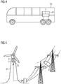
- the FIG 4 shows a vehicle 30, in this example a bus, but it could also be, for example, a passenger car, truck or a rail vehicle.
- This vehicle 30 has a converter 20 with a previously described semiconductor circuit 5.
- the converter 20 supplies the motors of the vehicle 30 and can control the acceleration or deceleration of the vehicle 30.
- the semiconductor 1 is switched off quickly and, above all, reliably. Damage to the converter 20 due to excessive currents in the event of a fault must be avoided in order to achieve high reliability and availability of the vehicle 30 and to prevent the vehicle 30 from lying down.
- the FIG 5 shows a wind turbine 40 for the production of electrical energy from wind.
- This energy is taken from the wind via rotor blades and converted by means of a converter 20 with one or more semiconductor circuits 5 in such a way that it can be fed into an energy supply network 41.
- a converter 20 with one or more semiconductor circuits 5 in such a way that it can be fed into an energy supply network 41.
- this wind power plant 40 it has proven to be advantageous to equip this wind power plant 40 with a semiconductor circuit 5 described above. This ensures that the semiconductors 1 (not shown here) are switched off quickly and, in particular in the event of a fault, prevents the semiconductors 1 from being damaged or destroyed by excessive currents.
- the invention relates to a method for controlling a large number of semiconductors by means of a control unit, a signal line being arranged between the control unit and the semiconductors, a protocol for controlling the semiconductors being transmitted via the signal line.
- a live signal is additionally transmitted via the signal line, the semiconductors being switched off when the live signal is absent.
- the invention further relates to a semiconductor circuit, comprising a multiplicity of semiconductors, each with a driver circuit and a control unit, a signal line being arranged between the control unit and the semiconductors, a protocol being provided via the signal line to control the semiconductors, wherein a live signal can also be transmitted via the signal line, and if the live signal is absent, the semiconductors can be switched off by means of the respective driver circuit.
- the invention further relates to a power converter with such a semiconductor circuit, the semiconductors or at least some of the semiconductors being arranged in a bridge circuit.
- the invention further relates to a vehicle and a wind turbine with such a converter.
Landscapes
- Engineering & Computer Science (AREA)
- Power Engineering (AREA)
- Mechanical Engineering (AREA)
- Electric Propulsion And Braking For Vehicles (AREA)
Abstract
Die Erfindung betrifft ein Verfahren zum Ansteuern einer Vielzahl von Halbleitern (1) durch eine Regelungseinheit (2), wobei zwischen der Regelungseinheit (2) und den Halbleitern (1) eine Signalleitung (3) angeordnet ist, wobei über die Signalleitung (3) ein Protokoll (11) zur Ansteuerung der Halbleiter (1) übertragen wird. Zur Verbesserung der Übertragung von Signalen von der Regelungseinheit zum Stromrichter hinsichtlich der Übertragungssicherheit wird vorgeschlagen, dass über die Signalleitung (3) zusätzlich ein Lebendsignal (12) übertragen wird, wobei bei Ausbleiben des Lebendsignals (12) die Halbleiter (1) abgeschaltet werden. Weiter betrifft die Erfindung eine Halbleiterschaltung (5), aufweisend eine Vielzahl von Halbleitern (1) mit jeweils einer Treiberschaltung (4) und eine Regelungseinheit (2), wobei zwischen der Regelungseinheit (2) und den Halbleitern (1) eine Signalleitung (3) angeordnet ist, wobei über die Signalleitung (3) ein Protokoll (11) zur Ansteuerung der Halbleiter (1) übertragbar ist, wobei über die Signalleitung (3) zusätzlich ein Lebendsignal (12) übertragbar ist, wobei bei Ausbleiben des Lebendsignals (12) die Halbleiter (1) mittels der jeweiligen Treiberschaltung (4) abschaltbar sind. Die Erfindung betrifft ferner einen Stromrichter (20) mit einer derartigen Halbleiterschaltung (5), wobei die Halbleiter (1) oder zumindest ein Teil der Halbleiter (1) in einer Brückenschaltung angeordnet sind. Die Erfindung betrifft weiter ein Fahrzeug (30) sowie eine Windenergieanlage (40) mit einem derartigen Stromrichter (20).The invention relates to a method for controlling a plurality of semiconductors (1) by means of a control unit (2), a signal line (3) being arranged between the control unit (2) and the semiconductors (1), with a signal line (3) Protocol (11) for controlling the semiconductor (1) is transmitted. In order to improve the transmission of signals from the control unit to the converter with regard to transmission security, it is proposed that an additional live signal (12) is transmitted via the signal line (3), the semiconductors (1) being switched off if the live signal (12) is not present. The invention further relates to a semiconductor circuit (5), comprising a multiplicity of semiconductors (1) each having a driver circuit (4) and a control unit (2), a signal line (3) between the control unit (2) and the semiconductors (1). A protocol (11) for controlling the semiconductors (1) can be transmitted via the signal line (3), a live signal (12) can also be transmitted via the signal line (3) Semiconductors (1) can be switched off by means of the respective driver circuit (4). The invention further relates to a converter (20) with such a semiconductor circuit (5), the semiconductors (1) or at least some of the semiconductors (1) being arranged in a bridge circuit. The invention further relates to a vehicle (30) and a wind energy installation (40) with such a converter (20).
Description
Die Erfindung betrifft ein Verfahren zum Ansteuern einer Vielzahl von Halbleitern durch eine Regelungseinheit, wobei zwischen der Regelungseinheit und den Halbleitern eine Signalleitung angeordnet ist, wobei über die Signalleitung ein Protokoll zur Ansteuerung der Halbleiter übertragen wird. Ferner betrifft die Erfindung eine Halbleiterschaltung mit einer Vielzahl von Halbleitern mit jeweils einer Treiberschaltung und einer Regelungseinheit, wobei zwischen der Regelungseinheit und den Halbleitern eine Signalleitung angeordnet ist, wobei über die Signalleitung ein Protokoll zur Ansteuerung der Halbleiter übertragbar ist. Die Erfindung betrifft weiter einen Stromrichter mit einer derartigen Halbleiterschaltung. Weiter betrifft die Erfindung ein Fahrzeug mit einem derartigen Stromrichter sowie eine Windenergieanlage mit einem derartigen Stromrichter.The invention relates to a method for controlling a large number of semiconductors by means of a control unit, a signal line being arranged between the control unit and the semiconductors, a protocol for controlling the semiconductors being transmitted via the signal line. Furthermore, the invention relates to a semiconductor circuit with a multiplicity of semiconductors, each with a driver circuit and a control unit, a signal line being arranged between the control unit and the semiconductors, a protocol for controlling the semiconductors being transferable via the signal line. The invention further relates to a converter with such a semiconductor circuit. The invention further relates to a vehicle with such a converter and to a wind energy installation with such a converter.
Um den Verdrahtungsaufwand innerhalb einer Halbleiterschaltung oder eines Stromrichters zu optimieren, wird zwischen der Regelungseinheit und den Halbleitern von einem parallelen Ansteuerverfahren auf ein serielles Ansteuerverfahren gewechselt. Während das parallele Ansteuerverfahren für jeden anzusteuernden Halbleiter jeweils eine Einzelansteuerleitung benötigt wird, werden diese Informationen bei dem seriellen Ansteuerverfahren auf nur einer Leitung gebündelt und mittels eines Protokolls, auch als Telegramm bezeichnet, übertragen. Die Halbleiter weisen dabei jeweils eine Treiberschaltung auf, die das für sie betreffende Signal, insbesondere bezüglich der Ansteuerung, d.h. Einschalten oder Ausschalten, auswertet und am Halbleiter umsetzt.In order to optimize the wiring effort within a semiconductor circuit or a converter, a switch is made between a control system and the semiconductors from a parallel control method to a serial control method. While the parallel control method requires a single control line for each semiconductor to be controlled, this information is bundled on only one line in the serial control method and transmitted using a protocol, also known as a telegram. The semiconductors each have a driver circuit which transmits the signal relevant to them, in particular with regard to the control, i.e. Switching on or off, evaluated and implemented on the semiconductor.
Der Erfindung liegt die Aufgabe zugrunde, die Übertragung von Signalen von der Regelungseinheit zum Stromrichter hinsichtlich der Übertragungssicherheit zu verbessern.The invention has for its object to improve the transmission of signals from the control unit to the converter with regard to the transmission security.
Diese Aufgabe wird durch ein Verfahren zum Ansteuern einer Vielzahl von Halbleitern durch eine Regelungseinheit dadurch gelöst, dass zwischen der Regelungseinheit und den Halbleitern eine Signalleitung angeordnet ist, wobei über die Signalleitung ein Protokoll zur Ansteuerung der Halbleiter übertragen wird, wobei über die Signalleitung zusätzlich ein Lebendsignal übertragen wird, wobei bei Ausbleiben des Lebendsignals die Halbleiter abgeschaltet werden. Ferner wird diese Aufgabe durch eine Halbleiterschaltung, aufweisend eine Vielzahl von Halbleitern mit jeweils einer Treiberschaltung und eine Regelungseinheit dadurch gelöst, dass zwischen der Regelungseinheit und den Halbleitern eine Signalleitung angeordnet ist, wobei über die Signalleitung ein Protokoll zur Ansteuerung der Halbleiter übertragbar ist, wobei über die Signalleitung zusätzlich ein Lebendsignal übertragbar ist, wobei bei Ausbleiben des Lebendsignals die Halbleiter mittels der jeweiligen Treiberschaltung abschaltbar sind. Diese Aufgabe wird weiter durch einen Stromrichter mit einer derartigen Halbleiterschaltung dadurch gelöst, dass die Halbleiter oder zumindest ein Teil der Halbleiter in einer Brückenschaltung angeordnet sind. Ferner wird diese Aufgabe durch ein Fahrzeug mit einem derartigen Stromrichter sowie durch eine Windenergieanlage mit einem derartigen Stromrichter gelöst.This object is achieved by a method for controlling a large number of semiconductors by means of a control unit in that a signal line is arranged between the control unit and the semiconductors, a protocol for controlling the semiconductors being transmitted via the signal line, a live signal additionally being transmitted via the signal line is transmitted, the semiconductors being switched off in the absence of the live signal. Furthermore, this object is achieved by a semiconductor circuit comprising a plurality of semiconductors, each with a driver circuit and a control unit, in that a signal line is arranged between the control unit and the semiconductors, a protocol for controlling the semiconductors being transferable via the signal line, the signal line can additionally transmit a live signal, the semiconductors being able to be switched off by means of the respective driver circuit if the live signal is absent. This object is further achieved by a power converter with such a semiconductor circuit in that the semiconductors or at least some of the semiconductors are arranged in a bridge circuit. Furthermore, this object is achieved by a vehicle with such a converter and by a wind energy installation with such a converter.
Weitere vorteilhafte Ausgestaltungen der Erfindung sind in den abhängigen Ansprüchen angegeben.Further advantageous embodiments of the invention are specified in the dependent claims.
Der Erfindung liegt die Erkenntnis zugrunde, dass sich die Übertragungssicherheit dadurch verbessern lässt, wenn ein Ausfall oder eine Störung der Signalübertragung der Signalübertragung zuverlässig und schnell erkannt wird. Üblicherweise wird eine Störung dann erkannt, wenn das Protokoll bzw. Telegramm ausgewertet wird. Dabei kann das Protokoll derart aufgebaut sein, Fehler in der Übertragung zu erkennen. Ein Beispiel für ein derartiges Telegramm ist eine CRC Kodierung. Durch die Verwendung von Telegrammen entstehen allerdings zur Bildung der Schaltinformation in der Halbleiterschaltung bzw. im Stromrichter Verzugszeiten, die eben auch auf ggf. erforderliche Schutzabschaltungen (detektiert und ausgeführt durch die Regelungseinheit) wirken. Dadurch ist ein ausreichendes Schutzkonzept des Umrichters nicht mehr gewährleistet, da Schutzabschaltzeiten zwischen ein und zwei Telegrammlängen entstehen. Die Fehlererkennungszeit bzw. die Anforderung zur Abschaltung der Halbleiter durch die Regelungseinheit als Schutzeingriff liegt damit in der Größenordnung von 5 µs bis 10 µs. In dieser Zeit können bereits Ströme in der Halbleiterschaltung bzw. im Stromrichter entstehen, die zur Beschädigung oder Zerstörung des Halbleiters bzw. Stromrichters führen.The invention is based on the finding that the transmission security can be improved if a failure or a disturbance in the signal transmission of the signal transmission is detected reliably and quickly. A fault is usually recognized when the protocol or telegram is evaluated. The protocol can be constructed in such a way that it recognizes errors in the transmission. An example of such a telegram is a CRC coding. The use of telegrams, however, results in delay times for the formation of the switching information in the semiconductor circuit or in the converter, which are also necessary Protective shutdowns (detected and executed by the control unit) act. As a result, a sufficient protection concept for the converter is no longer guaranteed, since protective switch-off times between one and two telegram lengths result. The error detection time or the requirement for the semiconductor to be switched off by the control unit as a protective intervention is thus in the order of 5 µs to 10 µs. During this time, currents can already occur in the semiconductor circuit or in the converter, which lead to damage or destruction of the semiconductor or converter.
Zur Lösung dieses Problems wird daher den seriellen Telegrammen zur Ansteuerung der Halbleiter auf derselben Signalleitung durch die Regelungseinheit ein Lebendsignal überlagert. Dies wird auf der Treiberschaltung des Halbleiters permanent auf Ausbleiben überwacht. Wenn es nicht mehr vorhanden ist, erfolgt ein Abschalten der Halbleiter durch die Treiberschaltung. Dabei kann es sich um einen Schutzeingriff oder ein betrieblich gewolltes schnelles Abschalten der Halbleiter handeln.To solve this problem, a live signal is therefore superimposed on the serial telegrams for controlling the semiconductors on the same signal line by the control unit. This is constantly monitored for absence on the driver circuit of the semiconductor. If it is no longer present, the semiconductor circuit is switched off by the driver circuit. This can be a protective intervention or an operationally desired fast shutdown of the semiconductors.
Ein von der Regelungseinheit zu initiierender Schutzeingriff wirkt ebenfalls direkt auf das Lebendsignal. Das Lebendsignal wird dann nicht mehr über die Signalleitung übertragen. Dies erkennt die Treiberschaltung des Halbleiters, so dass die Halbleiter unmittelbar abgeschaltet werden. Damit sind schnelle Schutzreaktionszeiten realisierbar, die mit denen der Einzelansteuerung vergleichbar sind. Der Anteil an Fehlerreaktionszeit durch die Kommunikation zwischen Regelungseinheit und Treiberschaltung wird damit auf die Größenordnung von 200 ns reduziert, mit der ein zuverlässiger Schutz der Halbleiterschaltung bzw. des Stromrichters sichergestellt werden kann.A protective intervention to be initiated by the control unit also has a direct effect on the live signal. The live signal is then no longer transmitted via the signal line. This detects the driver circuit of the semiconductor, so that the semiconductors are switched off immediately. This enables fast protection response times to be achieved, which are comparable to those of individual control. The proportion of error reaction time due to the communication between the control unit and the driver circuit is thus reduced to the order of magnitude of 200 ns, with which reliable protection of the semiconductor circuit or the converter can be ensured.
Auf diese Weise ist es möglich, Signale zur Ansteuerung der Halbleiter auf einer Signalleitung zu bündeln und gleichzeitig einen schnellen Schutz zu realisieren. Der Schutzeingriff ergibt sich dabei direkt von der Regelungseinheit initiiert, durch abschalten des Lebendsignals oder durch einen Fehler in der Übertragung, beispielsweise durch Kabelbruch der Signalleitung.In this way it is possible to bundle signals for controlling the semiconductors on one signal line and at the same time to implement rapid protection. The protective intervention results directly from the control unit, by switching off the live signal or by an error in the transmission, for example due to a broken cable in the signal line.
Bei einer vorteilhaften Ausgestaltung der Erfindung wird das Lebendsignal zyklisch oder dauerhaft übertragen. Damit der Empfänger, also der Halbleiter, genau weiß, wann ein Lebendsignal zu erwarten ist, um bei Ausbleiben eine Schutzabschaltung zu erwirken, ist es vorteilhaft, wenn das Lebendsignal zyklisch oder dauerhaft übertragen wird. Damit sind die Zeitpunkte, an denen ein Lebendsignal von der Treiberschaltung erwartet wird, bekannt und eine Schutzabschaltung kann besonders schnell erfolgen.In an advantageous embodiment of the invention, the live signal is transmitted cyclically or permanently. So that the receiver, that is to say the semiconductor, knows exactly when a live signal is to be expected in order to achieve a protective shutdown in the absence of a signal, it is advantageous if the live signal is transmitted cyclically or continuously. The times at which a live signal is expected from the driver circuit are thus known and a protective shutdown can take place particularly quickly.
Bei einer weiteren vorteilhaften Ausgestaltung der Erfindung wird das Lebendsignal als Manchester Code übertragen. Der Manchester-Code ist eine besonders einfache Kodierung, mit der ein Lebendsignal auf einer Signalleitung generiert werden kann. Entsprechende Baugruppen sind günstig am Markt verfügbar, so dass der Gewinn durch die Reduktion der Hardwareverdrahtung nur unwesentlich durch die Baugruppen zur Generierung des Manchester-Codes verringert wird. Somit kann eine Kostenreduktion bei der Herstellung der Halbleiterschaltung bzw. des Stromrichters erzielt werden. In einer vorteilhaften Ausgestaltung kann die Manchester-Codierung auch in die Hardware der Regelungseinheit und der Treiberschaltung oder eines Umsetzers integriert werden.In a further advantageous embodiment of the invention, the live signal is transmitted as a Manchester code. The Manchester code is a particularly simple coding with which a live signal can be generated on a signal line. Corresponding modules are available cheaply on the market, so that the profit from the reduction in hardware wiring is only insignificantly reduced by the modules for generating the Manchester code. A cost reduction in the manufacture of the semiconductor circuit or the converter can thus be achieved. In an advantageous embodiment, the Manchester coding can also be integrated into the hardware of the control unit and the driver circuit or a converter.
Bei einer weiteren vorteilhaften Ausgestaltung der Erfindung ist die Signalleitung als Lichtwellenleiter oder Bussystem ausgebildet. Sowohl Lichtwellenleiter als auch Bussystem stellen einfache und am Markt befindliche Lösungen zur Bündelung von Signalen dar. Diese können auf einfache Weise in die Halbleiterschaltung bzw. den Stromrichter integriert werden. Darüber hinaus bietet der Lichtwellenleiter zusätzlich noch den Vorteil der Potentialtrennung. Diese ist gerade für die Halbleiterschaltung bzw. Stromrichter mit einer Zwischenkreisspannung von mindestens 1500 V von Vorteil. Durch die Verwendung des Lichtwellenleiters ist eine Potentialverschleppung ausgeschlossen. Es wird zuverlässig verhindert, dass damit die Regelungseinheit mit unzulässig hohen Spannungen beaufschlagt wird. Da die Regelungsbaugruppe oftmals mit Bedienelementen elektrisch verbunden ist, wird damit auch die Beaufschlagung von unzulässig hohen Spannungen auf das Bedienelement verhindert und ein hinreichender Berührschutz sichergestellt. Dieser Berührschutz dient zur Vermeidung von Personenschäden.In a further advantageous embodiment of the invention, the signal line is designed as an optical waveguide or bus system. Both fiber optic cables and bus systems are simple solutions on the market for bundling signals. These can be easily integrated into the semiconductor circuit or the converter. In addition, the optical fiber also offers the advantage of potential isolation. This is just for the semiconductor circuit or converter with an intermediate circuit voltage of at least 1500 V is an advantage. The use of the fiber optic cable prevents potential carryover. This reliably prevents the control unit from being subjected to impermissibly high voltages. Since the control module is often electrically connected to operating elements, this also prevents impermissibly high voltages from being applied to the operating element and ensures adequate protection against contact. This contact protection is used to avoid personal injury.
Im Folgenden wird die Erfindung anhand der in den Figuren dargestellten Ausführungsbeispiele näher beschreiben und erläutert. Es zeigen:
- FIG 1
- den Aufbau der Halbleiterschaltung,
- FIG 2
- die zeitliche Reaktion bei der Übertragung eines Schutzeingriffs ohne Lebendsignal,
- FIG 3
- die zeitliche Reaktion bei der Übertragung eines Schutzeingriffs mit Lebendsignal,
- FIG 4
- ein Fahrzeug mit einer derartigen Halbleiterschaltung und
- FIG 5
- eine Windenergieanlage mit einer derartigen Halbleiterschaltung.
- FIG. 1
- the structure of the semiconductor circuit,
- FIG 2
- the time response when a protective intervention is transmitted without a live signal,
- FIG 3
- the time response when a protective intervention is transmitted with a live signal,
- FIG 4
- a vehicle with such a semiconductor circuit and
- FIG 5
- a wind turbine with such a semiconductor circuit.
Die
Die
Die
Die
Die
Zusammenfassend betrifft die Erfindung ein Verfahren zum Ansteuern einer Vielzahl von Halbleitern durch eine Regelungseinheit, wobei zwischen der Regelungseinheit und den Halbleitern eine Signalleitung angeordnet ist, wobei über die Signalleitung ein Protokoll zur Ansteuerung der Halbleiter übertragen wird. Zur Verbesserung der Übertragung von Signalen von der Regelungseinheit zum Stromrichter hinsichtlich der Übertragungssicherheit wird vorgeschlagen, dass über die Signalleitung zusätzlich ein Lebendsignal übertragen wird, wobei bei Ausbleiben des Lebendsignals die Halbleiter abgeschaltet werden. Weiter betrifft die Erfindung eine Halbleiterschaltung, aufweisend eine Vielzahl von Halbleitern mit jeweils einer Treiberschaltung und eine Regelungseinheit, wobei zwischen der Regelungseinheit und den Halbleitern eine Signalleitung angeordnet ist, wobei über die Signalleitung ein Protokoll zur Ansteuerung der Halbleiter übertragbar ist, wobei über die Signalleitung zusätzlich ein Lebendsignal übertragbar ist, wobei bei Ausbleiben des Lebendsignals die Halbleiter mittels der jeweiligen Treiberschaltung abschaltbar sind. Die Erfindung betrifft ferner einen Stromrichter mit einer derartigen Halbleiterschaltung, wobei die Halbleiter oder zumindest ein Teil der Halbleiter in einer Brückenschaltung angeordnet sind. Die Erfindung betrifft weiter ein Fahrzeug sowie eine Windenergieanlage mit einem derartigen Stromrichter.In summary, the invention relates to a method for controlling a large number of semiconductors by means of a control unit, a signal line being arranged between the control unit and the semiconductors, a protocol for controlling the semiconductors being transmitted via the signal line. In order to improve the transmission of signals from the control unit to the converter with regard to the transmission security, it is proposed that a live signal is additionally transmitted via the signal line, the semiconductors being switched off when the live signal is absent. The invention further relates to a semiconductor circuit, comprising a multiplicity of semiconductors, each with a driver circuit and a control unit, a signal line being arranged between the control unit and the semiconductors, a protocol being provided via the signal line to control the semiconductors, wherein a live signal can also be transmitted via the signal line, and if the live signal is absent, the semiconductors can be switched off by means of the respective driver circuit. The invention further relates to a power converter with such a semiconductor circuit, the semiconductors or at least some of the semiconductors being arranged in a bridge circuit. The invention further relates to a vehicle and a wind turbine with such a converter.
Claims (9)
Priority Applications (6)
| Application Number | Priority Date | Filing Date | Title |
|---|---|---|---|
| EP18213350.4A EP3672078A1 (en) | 2018-12-18 | 2018-12-18 | Method for controlling semiconductors |
| EP19829029.8A EP3861636A1 (en) | 2018-12-18 | 2019-12-12 | Method for controlling semiconductors |
| CN201980083929.6A CN113228512A (en) | 2018-12-18 | 2019-12-12 | Method for controlling a semiconductor |
| CA3123733A CA3123733A1 (en) | 2018-12-18 | 2019-12-12 | Method for controlling semiconductors |
| US17/415,495 US11909304B2 (en) | 2018-12-18 | 2019-12-12 | Method for controlling semiconductors |
| PCT/EP2019/084826 WO2020126796A1 (en) | 2018-12-18 | 2019-12-12 | Method for controlling semiconductors |
Applications Claiming Priority (1)
| Application Number | Priority Date | Filing Date | Title |
|---|---|---|---|
| EP18213350.4A EP3672078A1 (en) | 2018-12-18 | 2018-12-18 | Method for controlling semiconductors |
Publications (1)
| Publication Number | Publication Date |
|---|---|
| EP3672078A1 true EP3672078A1 (en) | 2020-06-24 |
Family
ID=64744590
Family Applications (2)
| Application Number | Title | Priority Date | Filing Date |
|---|---|---|---|
| EP18213350.4A Withdrawn EP3672078A1 (en) | 2018-12-18 | 2018-12-18 | Method for controlling semiconductors |
| EP19829029.8A Pending EP3861636A1 (en) | 2018-12-18 | 2019-12-12 | Method for controlling semiconductors |
Family Applications After (1)
| Application Number | Title | Priority Date | Filing Date |
|---|---|---|---|
| EP19829029.8A Pending EP3861636A1 (en) | 2018-12-18 | 2019-12-12 | Method for controlling semiconductors |
Country Status (5)
| Country | Link |
|---|---|
| US (1) | US11909304B2 (en) |
| EP (2) | EP3672078A1 (en) |
| CN (1) | CN113228512A (en) |
| CA (1) | CA3123733A1 (en) |
| WO (1) | WO2020126796A1 (en) |
Citations (4)
| Publication number | Priority date | Publication date | Assignee | Title |
|---|---|---|---|---|
| GB2483317A (en) * | 2011-01-12 | 2012-03-07 | Solaredge Technologies Ltd | Photovoltaic power generation system |
| DE102014219504A1 (en) * | 2014-09-26 | 2016-03-31 | Continental Automotive Gmbh | Wireless battery charging system with emergency shutdown for a driving battery of an electric vehicle |
| EP3029829A1 (en) * | 2014-12-05 | 2016-06-08 | Siemens Aktiengesellschaft | Method for joint transmission of control signals and digital data signals |
| DE102017103418A1 (en) * | 2017-02-20 | 2018-08-23 | Infineon Technologies Ag | A method of determining information about integrity of signal processing components within a signal path, signal processing circuit and electronic control unit |
Family Cites Families (9)
| Publication number | Priority date | Publication date | Assignee | Title |
|---|---|---|---|---|
| DE10026263B4 (en) * | 1999-08-27 | 2004-04-08 | Siemens Ag | Control method for an industrial technical system, in particular a machine tool or a robot |
| WO2013077249A1 (en) | 2011-11-22 | 2013-05-30 | 日本電信電話株式会社 | Self-diagnostic method for pon protection system, and pon protection system |
| CN103683870B (en) * | 2012-08-29 | 2017-04-12 | 通用电气公司 | Improved converter modulation system and method |
| DE102012220582A1 (en) | 2012-11-12 | 2014-07-03 | Wobben Properties Gmbh | Wind energy plant and method for feeding electrical energy |
| JP6441343B2 (en) * | 2013-08-06 | 2018-12-19 | ボルボ トラック コーポレイション | Hybrid vehicle |
| EP2905888A1 (en) | 2014-02-05 | 2015-08-12 | Grundfos Holding A/S | Inverter |
| CN104158853A (en) * | 2014-07-23 | 2014-11-19 | 中国人民解放军海军工程大学 | Manchester-code-based power electronic conversion system communication control framework |
| FR3036237B1 (en) * | 2015-05-11 | 2018-06-01 | Schneider Toshiba Inverter Europe Sas | MULTINIVEAL MEDIUM VOLTAGE POWER CONVERTING DEVICE WITH ALTERNATIVE OUTPUT |
| US10762182B2 (en) | 2017-02-20 | 2020-09-01 | Novatek Microelectronics Corp. | Detection system, fingerprint sensor, and method of finger touch authentication thereof |
-
2018
- 2018-12-18 EP EP18213350.4A patent/EP3672078A1/en not_active Withdrawn
-
2019
- 2019-12-12 EP EP19829029.8A patent/EP3861636A1/en active Pending
- 2019-12-12 CN CN201980083929.6A patent/CN113228512A/en active Pending
- 2019-12-12 US US17/415,495 patent/US11909304B2/en active Active
- 2019-12-12 CA CA3123733A patent/CA3123733A1/en active Pending
- 2019-12-12 WO PCT/EP2019/084826 patent/WO2020126796A1/en active Search and Examination
Patent Citations (4)
| Publication number | Priority date | Publication date | Assignee | Title |
|---|---|---|---|---|
| GB2483317A (en) * | 2011-01-12 | 2012-03-07 | Solaredge Technologies Ltd | Photovoltaic power generation system |
| DE102014219504A1 (en) * | 2014-09-26 | 2016-03-31 | Continental Automotive Gmbh | Wireless battery charging system with emergency shutdown for a driving battery of an electric vehicle |
| EP3029829A1 (en) * | 2014-12-05 | 2016-06-08 | Siemens Aktiengesellschaft | Method for joint transmission of control signals and digital data signals |
| DE102017103418A1 (en) * | 2017-02-20 | 2018-08-23 | Infineon Technologies Ag | A method of determining information about integrity of signal processing components within a signal path, signal processing circuit and electronic control unit |
Also Published As
| Publication number | Publication date |
|---|---|
| WO2020126796A1 (en) | 2020-06-25 |
| US11909304B2 (en) | 2024-02-20 |
| US20220052598A1 (en) | 2022-02-17 |
| CN113228512A (en) | 2021-08-06 |
| EP3861636A1 (en) | 2021-08-11 |
| CA3123733A1 (en) | 2020-06-25 |
Similar Documents
| Publication | Publication Date | Title |
|---|---|---|
| EP2745327B1 (en) | Socket for a solar panel with a protective circuit | |
| EP2284973B1 (en) | Reverse current sensor for solar modules connected in parallel | |
| EP2720094B1 (en) | Safety system | |
| WO2016075106A1 (en) | Motor vehicle supply network | |
| EP2652857A1 (en) | Method for disconnecting a photovoltaic assembly and photovoltaic assembly | |
| EP2980660B1 (en) | Method and device for monitoring and switching a load circuit | |
| EP2720051A1 (en) | Safety system | |
| EP1967831B1 (en) | Temperature release device | |
| AT17880U1 (en) | INVERTER | |
| DE69636743T2 (en) | Power semiconductor module and composite power module | |
| EP3084949B1 (en) | Method for actuating inverters connected in parallel | |
| DE102014019725C5 (en) | Electronic switching device and electronic switching method | |
| EP0778467A2 (en) | Circuit for monitoring grounding and protection against dangerous currents through the human body, especially for devices with potential equalisation in star-star networks | |
| EP3672078A1 (en) | Method for controlling semiconductors | |
| DE19947501C5 (en) | Actuator Sensor Interface slave | |
| DE102012023460A1 (en) | Onboard supply system i.e. 2 volt-onboard supply system, for use in e.g. passenger car, has battery supplying current to network area, and arc control device detecting arc from current difference between current measured in measuring units | |
| EP2456034B1 (en) | Photovoltaic assembly and photovoltaic module | |
| EP2770641B1 (en) | Device for the evaluation of electrical input signals | |
| EP3776786B1 (en) | Monitoring of a high-voltage dc transmission | |
| WO2016062580A1 (en) | Control device for a multi-voltage on-board power supply | |
| DE102015110285B4 (en) | Arrangement and method for discharging a high-voltage circuit of an inverter | |
| EP3672009B1 (en) | Protection circuit, electronic device and method for operating an electronic device | |
| EP4292182B1 (en) | System and monitoring field device | |
| DE102019118180B4 (en) | Data bus system for a vehicle | |
| WO2024028442A1 (en) | Photovoltaic system with safety deactivation function |
Legal Events
| Date | Code | Title | Description |
|---|---|---|---|
| PUAI | Public reference made under article 153(3) epc to a published international application that has entered the european phase |
Free format text: ORIGINAL CODE: 0009012 |
|
| STAA | Information on the status of an ep patent application or granted ep patent |
Free format text: STATUS: THE APPLICATION HAS BEEN PUBLISHED |
|
| AK | Designated contracting states |
Kind code of ref document: A1 Designated state(s): AL AT BE BG CH CY CZ DE DK EE ES FI FR GB GR HR HU IE IS IT LI LT LU LV MC MK MT NL NO PL PT RO RS SE SI SK SM TR |
|
| AX | Request for extension of the european patent |
Extension state: BA ME |
|
| STAA | Information on the status of an ep patent application or granted ep patent |
Free format text: STATUS: THE APPLICATION IS DEEMED TO BE WITHDRAWN |
|
| 18D | Application deemed to be withdrawn |
Effective date: 20210112 |