EP3553928A1 - Snubber circuit and power conversion system using same - Google Patents
Snubber circuit and power conversion system using same Download PDFInfo
- Publication number
- EP3553928A1 EP3553928A1 EP17882036.1A EP17882036A EP3553928A1 EP 3553928 A1 EP3553928 A1 EP 3553928A1 EP 17882036 A EP17882036 A EP 17882036A EP 3553928 A1 EP3553928 A1 EP 3553928A1
- Authority
- EP
- European Patent Office
- Prior art keywords
- voltage
- circuit
- clamp
- pair
- points
- Prior art date
- Legal status (The legal status is an assumption and is not a legal conclusion. Google has not performed a legal analysis and makes no representation as to the accuracy of the status listed.)
- Granted
Links
- 238000006243 chemical reaction Methods 0.000 title claims abstract description 100
- 239000004065 semiconductor Substances 0.000 claims description 30
- 238000004804 winding Methods 0.000 description 27
- 239000003990 capacitor Substances 0.000 description 18
- 230000014509 gene expression Effects 0.000 description 14
- 238000010586 diagram Methods 0.000 description 13
- 101100509369 Caenorhabditis elegans isw-1 gene Proteins 0.000 description 10
- 230000003071 parasitic effect Effects 0.000 description 9
- 230000007423 decrease Effects 0.000 description 7
- 238000013459 approach Methods 0.000 description 2
- 238000007599 discharging Methods 0.000 description 2
- 239000004020 conductor Substances 0.000 description 1
- 230000001934 delay Effects 0.000 description 1
- 230000005611 electricity Effects 0.000 description 1
- 239000000284 extract Substances 0.000 description 1
- 230000005669 field effect Effects 0.000 description 1
- 239000000446 fuel Substances 0.000 description 1
- 230000017525 heat dissipation Effects 0.000 description 1
- 230000020169 heat generation Effects 0.000 description 1
- 238000012986 modification Methods 0.000 description 1
- 230000004048 modification Effects 0.000 description 1
- 230000001172 regenerating effect Effects 0.000 description 1
- 230000008929 regeneration Effects 0.000 description 1
- 238000011069 regeneration method Methods 0.000 description 1
- 230000000630 rising effect Effects 0.000 description 1
- 230000000087 stabilizing effect Effects 0.000 description 1
Images


Classifications
-
- H—ELECTRICITY
- H02—GENERATION; CONVERSION OR DISTRIBUTION OF ELECTRIC POWER
- H02M—APPARATUS FOR CONVERSION BETWEEN AC AND AC, BETWEEN AC AND DC, OR BETWEEN DC AND DC, AND FOR USE WITH MAINS OR SIMILAR POWER SUPPLY SYSTEMS; CONVERSION OF DC OR AC INPUT POWER INTO SURGE OUTPUT POWER; CONTROL OR REGULATION THEREOF
- H02M1/00—Details of apparatus for conversion
- H02M1/32—Means for protecting converters other than automatic disconnection
- H02M1/34—Snubber circuits
- H02M1/342—Active non-dissipative snubbers
-
- H—ELECTRICITY
- H02—GENERATION; CONVERSION OR DISTRIBUTION OF ELECTRIC POWER
- H02M—APPARATUS FOR CONVERSION BETWEEN AC AND AC, BETWEEN AC AND DC, OR BETWEEN DC AND DC, AND FOR USE WITH MAINS OR SIMILAR POWER SUPPLY SYSTEMS; CONVERSION OF DC OR AC INPUT POWER INTO SURGE OUTPUT POWER; CONTROL OR REGULATION THEREOF
- H02M1/00—Details of apparatus for conversion
- H02M1/32—Means for protecting converters other than automatic disconnection
- H02M1/34—Snubber circuits
-
- H—ELECTRICITY
- H02—GENERATION; CONVERSION OR DISTRIBUTION OF ELECTRIC POWER
- H02M—APPARATUS FOR CONVERSION BETWEEN AC AND AC, BETWEEN AC AND DC, OR BETWEEN DC AND DC, AND FOR USE WITH MAINS OR SIMILAR POWER SUPPLY SYSTEMS; CONVERSION OF DC OR AC INPUT POWER INTO SURGE OUTPUT POWER; CONTROL OR REGULATION THEREOF
- H02M3/00—Conversion of dc power input into dc power output
- H02M3/22—Conversion of dc power input into dc power output with intermediate conversion into ac
- H02M3/24—Conversion of dc power input into dc power output with intermediate conversion into ac by static converters
- H02M3/28—Conversion of dc power input into dc power output with intermediate conversion into ac by static converters using discharge tubes with control electrode or semiconductor devices with control electrode to produce the intermediate ac
- H02M3/325—Conversion of dc power input into dc power output with intermediate conversion into ac by static converters using discharge tubes with control electrode or semiconductor devices with control electrode to produce the intermediate ac using devices of a triode or a transistor type requiring continuous application of a control signal
- H02M3/335—Conversion of dc power input into dc power output with intermediate conversion into ac by static converters using discharge tubes with control electrode or semiconductor devices with control electrode to produce the intermediate ac using devices of a triode or a transistor type requiring continuous application of a control signal using semiconductor devices only
- H02M3/33569—Conversion of dc power input into dc power output with intermediate conversion into ac by static converters using discharge tubes with control electrode or semiconductor devices with control electrode to produce the intermediate ac using devices of a triode or a transistor type requiring continuous application of a control signal using semiconductor devices only having several active switching elements
- H02M3/33576—Conversion of dc power input into dc power output with intermediate conversion into ac by static converters using discharge tubes with control electrode or semiconductor devices with control electrode to produce the intermediate ac using devices of a triode or a transistor type requiring continuous application of a control signal using semiconductor devices only having several active switching elements having at least one active switching element at the secondary side of an isolation transformer
- H02M3/33584—Bidirectional converters
-
- H—ELECTRICITY
- H02—GENERATION; CONVERSION OR DISTRIBUTION OF ELECTRIC POWER
- H02M—APPARATUS FOR CONVERSION BETWEEN AC AND AC, BETWEEN AC AND DC, OR BETWEEN DC AND DC, AND FOR USE WITH MAINS OR SIMILAR POWER SUPPLY SYSTEMS; CONVERSION OF DC OR AC INPUT POWER INTO SURGE OUTPUT POWER; CONTROL OR REGULATION THEREOF
- H02M3/00—Conversion of dc power input into dc power output
- H02M3/22—Conversion of dc power input into dc power output with intermediate conversion into ac
- H02M3/24—Conversion of dc power input into dc power output with intermediate conversion into ac by static converters
- H02M3/28—Conversion of dc power input into dc power output with intermediate conversion into ac by static converters using discharge tubes with control electrode or semiconductor devices with control electrode to produce the intermediate ac
- H02M3/325—Conversion of dc power input into dc power output with intermediate conversion into ac by static converters using discharge tubes with control electrode or semiconductor devices with control electrode to produce the intermediate ac using devices of a triode or a transistor type requiring continuous application of a control signal
- H02M3/335—Conversion of dc power input into dc power output with intermediate conversion into ac by static converters using discharge tubes with control electrode or semiconductor devices with control electrode to produce the intermediate ac using devices of a triode or a transistor type requiring continuous application of a control signal using semiconductor devices only
- H02M3/337—Conversion of dc power input into dc power output with intermediate conversion into ac by static converters using discharge tubes with control electrode or semiconductor devices with control electrode to produce the intermediate ac using devices of a triode or a transistor type requiring continuous application of a control signal using semiconductor devices only in push-pull configuration
- H02M3/3376—Conversion of dc power input into dc power output with intermediate conversion into ac by static converters using discharge tubes with control electrode or semiconductor devices with control electrode to produce the intermediate ac using devices of a triode or a transistor type requiring continuous application of a control signal using semiconductor devices only in push-pull configuration with automatic control of output voltage or current
-
- H—ELECTRICITY
- H02—GENERATION; CONVERSION OR DISTRIBUTION OF ELECTRIC POWER
- H02M—APPARATUS FOR CONVERSION BETWEEN AC AND AC, BETWEEN AC AND DC, OR BETWEEN DC AND DC, AND FOR USE WITH MAINS OR SIMILAR POWER SUPPLY SYSTEMS; CONVERSION OF DC OR AC INPUT POWER INTO SURGE OUTPUT POWER; CONTROL OR REGULATION THEREOF
- H02M7/00—Conversion of ac power input into dc power output; Conversion of dc power input into ac power output
- H02M7/42—Conversion of dc power input into ac power output without possibility of reversal
- H02M7/44—Conversion of dc power input into ac power output without possibility of reversal by static converters
- H02M7/48—Conversion of dc power input into ac power output without possibility of reversal by static converters using discharge tubes with control electrode or semiconductor devices with control electrode
- H02M7/53—Conversion of dc power input into ac power output without possibility of reversal by static converters using discharge tubes with control electrode or semiconductor devices with control electrode using devices of a triode or transistor type requiring continuous application of a control signal
- H02M7/537—Conversion of dc power input into ac power output without possibility of reversal by static converters using discharge tubes with control electrode or semiconductor devices with control electrode using devices of a triode or transistor type requiring continuous application of a control signal using semiconductor devices only, e.g. single switched pulse inverters
- H02M7/5387—Conversion of dc power input into ac power output without possibility of reversal by static converters using discharge tubes with control electrode or semiconductor devices with control electrode using devices of a triode or transistor type requiring continuous application of a control signal using semiconductor devices only, e.g. single switched pulse inverters in a bridge configuration
-
- H—ELECTRICITY
- H02—GENERATION; CONVERSION OR DISTRIBUTION OF ELECTRIC POWER
- H02M—APPARATUS FOR CONVERSION BETWEEN AC AND AC, BETWEEN AC AND DC, OR BETWEEN DC AND DC, AND FOR USE WITH MAINS OR SIMILAR POWER SUPPLY SYSTEMS; CONVERSION OF DC OR AC INPUT POWER INTO SURGE OUTPUT POWER; CONTROL OR REGULATION THEREOF
- H02M1/00—Details of apparatus for conversion
- H02M1/0067—Converter structures employing plural converter units, other than for parallel operation of the units on a single load
- H02M1/007—Plural converter units in cascade
-
- H—ELECTRICITY
- H02—GENERATION; CONVERSION OR DISTRIBUTION OF ELECTRIC POWER
- H02M—APPARATUS FOR CONVERSION BETWEEN AC AND AC, BETWEEN AC AND DC, OR BETWEEN DC AND DC, AND FOR USE WITH MAINS OR SIMILAR POWER SUPPLY SYSTEMS; CONVERSION OF DC OR AC INPUT POWER INTO SURGE OUTPUT POWER; CONTROL OR REGULATION THEREOF
- H02M3/00—Conversion of dc power input into dc power output
- H02M3/02—Conversion of dc power input into dc power output without intermediate conversion into ac
- H02M3/04—Conversion of dc power input into dc power output without intermediate conversion into ac by static converters
- H02M3/10—Conversion of dc power input into dc power output without intermediate conversion into ac by static converters using discharge tubes with control electrode or semiconductor devices with control electrode
- H02M3/145—Conversion of dc power input into dc power output without intermediate conversion into ac by static converters using discharge tubes with control electrode or semiconductor devices with control electrode using devices of a triode or transistor type requiring continuous application of a control signal
- H02M3/155—Conversion of dc power input into dc power output without intermediate conversion into ac by static converters using discharge tubes with control electrode or semiconductor devices with control electrode using devices of a triode or transistor type requiring continuous application of a control signal using semiconductor devices only
- H02M3/156—Conversion of dc power input into dc power output without intermediate conversion into ac by static converters using discharge tubes with control electrode or semiconductor devices with control electrode using devices of a triode or transistor type requiring continuous application of a control signal using semiconductor devices only with automatic control of output voltage or current, e.g. switching regulators
- H02M3/158—Conversion of dc power input into dc power output without intermediate conversion into ac by static converters using discharge tubes with control electrode or semiconductor devices with control electrode using devices of a triode or transistor type requiring continuous application of a control signal using semiconductor devices only with automatic control of output voltage or current, e.g. switching regulators including plural semiconductor devices as final control devices for a single load
-
- H—ELECTRICITY
- H02—GENERATION; CONVERSION OR DISTRIBUTION OF ELECTRIC POWER
- H02M—APPARATUS FOR CONVERSION BETWEEN AC AND AC, BETWEEN AC AND DC, OR BETWEEN DC AND DC, AND FOR USE WITH MAINS OR SIMILAR POWER SUPPLY SYSTEMS; CONVERSION OF DC OR AC INPUT POWER INTO SURGE OUTPUT POWER; CONTROL OR REGULATION THEREOF
- H02M7/00—Conversion of ac power input into dc power output; Conversion of dc power input into ac power output
- H02M7/66—Conversion of ac power input into dc power output; Conversion of dc power input into ac power output with possibility of reversal
- H02M7/68—Conversion of ac power input into dc power output; Conversion of dc power input into ac power output with possibility of reversal by static converters
- H02M7/72—Conversion of ac power input into dc power output; Conversion of dc power input into ac power output with possibility of reversal by static converters using discharge tubes with control electrode or semiconductor devices with control electrode
- H02M7/79—Conversion of ac power input into dc power output; Conversion of dc power input into ac power output with possibility of reversal by static converters using discharge tubes with control electrode or semiconductor devices with control electrode using devices of a triode or transistor type requiring continuous application of a control signal
- H02M7/797—Conversion of ac power input into dc power output; Conversion of dc power input into ac power output with possibility of reversal by static converters using discharge tubes with control electrode or semiconductor devices with control electrode using devices of a triode or transistor type requiring continuous application of a control signal using semiconductor devices only
-
- Y—GENERAL TAGGING OF NEW TECHNOLOGICAL DEVELOPMENTS; GENERAL TAGGING OF CROSS-SECTIONAL TECHNOLOGIES SPANNING OVER SEVERAL SECTIONS OF THE IPC; TECHNICAL SUBJECTS COVERED BY FORMER USPC CROSS-REFERENCE ART COLLECTIONS [XRACs] AND DIGESTS
- Y02—TECHNOLOGIES OR APPLICATIONS FOR MITIGATION OR ADAPTATION AGAINST CLIMATE CHANGE
- Y02B—CLIMATE CHANGE MITIGATION TECHNOLOGIES RELATED TO BUILDINGS, e.g. HOUSING, HOUSE APPLIANCES OR RELATED END-USER APPLICATIONS
- Y02B70/00—Technologies for an efficient end-user side electric power management and consumption
- Y02B70/10—Technologies improving the efficiency by using switched-mode power supplies [SMPS], i.e. efficient power electronics conversion e.g. power factor correction or reduction of losses in power supplies or efficient standby modes
Definitions
- the present disclosure generally relates to snubber circuits and power conversion systems including the snubber circuits, and specifically to a snubber circuit for suppressing a ringing or surge voltage and a power conversion system including the snubber circuit.
- Patent Literature 1 describes a snubber circuit used in a power conversion system such as an alternating-current/direct-current power converter.
- an AC/AC frequency converter connected to a primary side of a high-frequency transformer includes a three-phase rectifier, an inverter, and a snubber circuit.
- the three-phase rectifier has an input side connected to a three-phase commercial AC power supply and an output side connected to an input side of the inverter.
- the input side of the inverter is connected to the output side of the three-phase rectifier, and an output side of the inverter is connected to the primary side of the high-frequency transformer.
- the snubber circuit is connected between the three-phase rectifier and the inverter.
- the snubber circuit described in Patent Literature 1 absorbs, as energy, a spike-like overvoltage caused due to leakage inductance of the high-frequency transformer and regenerates the energy absorbed.
- the snubber circuit is an RCD single direction snubber circuit of regenerative type including a resistor, a capacitor, a diode, and a semiconductor switch.
- Patent Literature 1 JP 2013-158064 A
- a snubber circuit of a first aspect includes a first clamp circuit, a second clamp circuit, and a voltage conversion circuit.
- the first clamp circuit is configured to, when a magnitude of a voltage between a pair of first voltage points in a main circuit exceeds a first clamp value, absorb electrical energy of the main circuit from the pair of first voltage points. Thus, the first clamp circuit clamps the voltage between the pair of first voltage points to the first clamp value.
- the second clamp circuit is configured to, when a magnitude of a voltage between a pair of second voltage points in the main circuit falls below a second clamp value, inject electrical energy to the main circuit from the pair of second voltage points. Thus, the second clamp circuit clamps the voltage between the pair of second voltage points to the second clamp value.
- the voltage conversion circuit is electrically connected to the first clamp circuit and the second clamp circuit and is configured to perform voltage conversion between a first clamp voltage and a second clamp voltage.
- the first clamp voltage defines the first clamp value.
- the second clamp voltage defines the second clamp value.
- one first voltage point of the pair of first voltage points is located on a high-potential side
- one second voltage point of the pair of second voltage points is located on the high-potential side
- a potential at the one first voltage point is equal to a potential at the one second voltage point.
- the other first voltage point of the pair of first voltage points is located on a low-potential side
- the other second voltage point of the pair of second voltage points is located on the low-potential side
- a potential at the other first voltage point is equal to a potential at the other second voltage point.
- the voltage conversion circuit is configured to step down the first clamp voltage to generate the second clamp voltage.
- the voltage conversion circuit is a DC/DC converter including a semiconductor switch, an inductor, and a capacitive element.
- the capacitive element is electrically connected in parallel to at least one of the semiconductor switch and the inductor.
- the first clamp circuit includes a first diode and a first capacitive element which are electrically connected in series between the pair of first voltage points.
- the first clamp circuit is configured to, when the voltage between the pair of first voltage points exceeds the first clamp value, cause a current to flow from the main circuit through the first diode to the first capacitive element.
- the second clamp circuit includes a second diode and a second capacitive element which are electrically connected in series between the pair of second voltage points.
- the second clamp circuit is configured to, when the voltage between the pair of second voltage points falls below the second clamp value, cause a current to flow from the second capacitive element through the second diode to the main circuit.
- the voltage conversion circuit is a DC/DC converter including a semiconductor switch and an inductor.
- the voltage conversion circuit is configured to cause the semiconductor switch to perform switching operation such that an inductor current flowing through the inductor is in a discontinuous mode.
- the voltage conversion circuit is a DC/DC converter including a semiconductor switch, an inductor, and a control circuit configured to control the semiconductor switch.
- the control circuit is configured to adjust a duty ratio of the semiconductor switch to adjust the first clamp value and the second clamp value.
- a power conversion system of a seventh aspect includes the snubber circuit of any one of the first to sixth aspects, and the main circuit.
- the main circuit being a power conversion circuit configured to convert electric power.
- the main circuit includes two or more primary-side terminals, two or more secondary-side terminals, and a high-frequency insulated transformer.
- the main circuit is configured to convert electric power between a set of the two or more primary-side terminals and a set of the two or more secondary-side terminals via the high-frequency insulated transformer.
- the snubber circuit is electrically connected to the high-frequency insulated transformer.
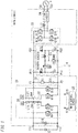
- a power conversion system 1 includes a main circuit 2 and a snubber circuit 3.
- the main circuit 2 is a power conversion circuit configured to convert electric power.
- the snubber circuit 3 is a protection circuit configured to control a ringing or surge voltage generated by the main circuit 2.
- the power conversion system 1 according to the present embodiment enables such ringing to be suppressed by the snubber circuit 3.
- the snubber circuit 3 corresponds to a sub-circuit with respect to the main circuit 2.
- the power conversion system 1 is used for electric power conversion, for example, between a power system 4 and a storage battery 5 as illustrated in FIG. 1 .
- the term "power system” means an entire system based on which an electricity supplier such as an electric power company supplies electric power to a power receiving facility of a consumer.
- the power conversion system 1 includes a pair of primary-side terminals T11 and T12 to which the storage battery 5 is electrically connected and a pair of secondary-side terminals T21 and T22 to which the power system 4 is electrically connected.
- the power conversion system 1 converts alternating-current power input from the power system 4 into direct-current power and supplies the direct-current power to the storage battery 5 so as to charge the storage battery 5.
- the power conversion system 1 converts direct-current power input from the storage battery 5 into alternating-current power and outputs the alternating-current power to the power system 4 so as to discharge the storage battery 5.
- the power conversion system 1 is configured to bidirectionally convert electric power between the pair of primary-side terminals T11 and T12 and the pair of secondary-side terminals T21 and T22 so as to be compatible with both charging and discharging of the storage battery 5.
- the power conversion system 1 connects and systematically links the storage battery 5 to the power system 4 to enable the storage battery 5 to be charged with electric power supplied from the power system 4 and/or to enable a load connected to the power system 4 to be supplied with discharged electric power of the storage battery 5.
- the main circuit 2 includes the pair of primary-side terminals T11 and T12, the pair of secondary-side terminals T21 and T22, a capacitor C10, a first converter 21, a second converter 22, an RC snubber 23, a filter circuit 24, a main control circuit 25, and an inductor L10.
- the storage battery 5 is electrically connected between the pair of primary-side terminals T11 and T12 such that the primary-side terminal T11 is located on a high-potential (positive-electrode) side.
- the power system 4 is electrically connected between the pair of secondary-side terminals T21 and T22.
- terminal does not have to be a component for connecting an electric wire and the like but may be, for example, a lead of an electronic component or part of a conductor included in a circuit board.
- the capacitor C10 is, in this embodiment, an electrolytic capacitor and is electrically connected between the pair of primary-side terminals T11 and T12.
- the capacitor C10 has a function of stabilizing a voltage between the pair of primary-side terminals T11 and T12.
- the RC snubber 23 includes a resistor R1 and a capacitor C11.
- the resistor R1 and the capacitor C11 are electrically connected in series between a pair of bus voltage points P1 and P2.
- the snubber circuit 3 is electrically connected between the pair of bus voltage points P1 and P2, which will be described later in detail. While the main circuit 2 operates, a bus voltage Vbus which is a direct-current voltage is generated between the pair of bus voltage points P1 and P2.
- the first converter 21 is electrically connected between the capacitor C10 and the RC snubber 23.
- the first converter 21 includes a transformer 26 and first to fourth switching elements Q11 to Q14.
- the first converter 21 serves as an insulating DC/DC converter located between the capacitor C10 and the RC snubber 23 and configured to convert a direct-current voltage.
- each of the first to fourth switching elements Q11 to Q14 is an n-channel depletion Metal-Oxide-Semiconductor Field Effect Transistor (MOSFET).
- the transformer 26 includes a primary winding wire 261 and a secondary winding wire 262 which are magnetically connected to each other.
- the transformer 26 is a high-frequency insulated transformer equipped with a center tap.
- the primary winding wire 261 includes a series circuit of two winding wires L11 and L12 with a primary side center tap 263 as a connection point.
- the secondary winding wire 262 includes a series circuit of two winding wires L21 and L22 with a secondary side center tap 264 as a connection point.
- the primary side center tap 263 is electrically connected to a positive electrode-side terminal (the primary-side terminal T11) of the capacitor C10.
- the secondary side center tap 264 is electrically connected to the bus voltage point P1 of the pair of bus voltage points P1 and P2 which is on a high-potential side.
- the winding turns ratio of the winding wires L11, L12, L21, and L22 is 1:1:1:1.
- the first switching element Q11 is electrically connected in series to the winding wire L11 between both ends of the capacitor C10.
- the second switching element Q12 is electrically connected in series to the winding wire L12 between both the ends of the capacitor C10.
- a series circuit of the winding wire L11 and the first switching element Q11 and a series circuit of the winding wire L12 and the second switching element Q12 are electrically connected in parallel.
- the drain of the first switching element Q11 is electrically connected to the primary side center tap 263 via the winding wire L11
- the drain of the second switching element Q12 is electrically connected to the primary side center tap 263 via the winding wire L12.
- the source of the first switching element Q11 and the source of the second switching element Q12 are both electrically connected to a negative electrode-side terminal (the primary-side terminal T12) of the capacitor C10.
- the third switching element Q13 is electrically connected in series to the winding wire L21 between both ends of the RC snubber 23.
- the fourth switching element Q14 is electrically connected in series to the winding wire L22 between both the ends of the RC snubber 23.
- a series circuit of the winding wire L21 and the third switching element Q13 and a series circuit of the winding wire L22 and the fourth switching element Q14 are electrically connected in parallel.
- the drain of the third switching element Q13 is electrically connected to the secondary side center tap 264 via the winding wire L21
- the drain of the fourth switching element Q14 is electrically connected to the secondary side center tap 264 via the winding wire L22.
- the source of the third switching element Q13 and the source of the fourth switching element Q14 are both electrically connected to the bus voltage point P2 of the pair of bus voltage points P1 and P2 which is on a low-potential side.
- the second converter 22 is electrically connected between the RC snubber 23 and the pair of secondary-side terminals T21 and T22.
- the second converter 22 includes fifth to eighth switching elements Q15 to Q18.
- the second converter 22 serves as a DC/AC converter (inverter) located between the RC snubber 23 and the filter circuit 24 and configured to convert the direct-current voltage into an alternating-current voltage, or the alternating-current voltage into the direct-current voltage.
- each of the fifth to eighth switching elements Q15 to Q18 is an n-channel depletion MOSFET.
- the fifth to eighth switching elements Q15 to Q18 are connected in a full-bridge configuration. That is, between both the ends of the RC snubber 23, the fifth switching element Q15 is electrically connected in series to the sixth switching element Q16. Between both the ends of the RC snubber 23, the seventh switching element Q17 is electrically connected in series to the eighth switching element Q18. In other words, between the pair of bus voltage points P1 and P2, a series circuit of the fifth switching element Q15 and the sixth switching element Q16 is electrically connected in parallel to a series circuit of the seventh switching element Q17 and the eighth switching element Q18.
- the drain of the fifth switching element Q15 and the drain of the seventh switching element Q17 are both electrically connected to the bus voltage point P1 of the pair of bus voltage points P1 and P2 which is on the high-potential side.
- the source of the sixth switching element Q16 and the source of the eighth switching element Q18 are both electrically connected to the bus voltage point P2 of the pair of bus voltage points P1 and P2 which is on the low-potential side.
- the filter circuit 24 is electrically connected between the second converter 22 and the pair of secondary-side terminals T21 and T22. Specifically, the filter circuit 24 has a pair of terminals facing the second converter 22, and one of the pair of terminals is electrically connected via the inductor L10 to a connection point of the source of the fifth switching element Q15 and the drain of the sixth switching element Q16. The filter circuit 24 has the pair of terminals facing the second converter 22, and the other of the pair of terminals is electrically connected to a connection point of the source of the seventh switching element Q17 and the drain of the eighth switching element Q18. The filter circuit 24 has a pair of terminals facing the secondary-side terminals T21 and T22 and electrically connected to the pair of secondary-side terminals T21 and T22. In other words, the second converter 22 is electrically connected via the inductor L10 and the filter circuit 24 to the pair of secondary-side terminals T21 and T22.
- the main control circuit 25 outputs control signals S11 to S18 for controlling the first to eighth switching elements Q11 to Q18.
- the control signals S11 to S18 are respectively applied to the gates of the first to eighth switching elements Q11 to Q18 directly or via a drive circuit so as to individually turn on/off the first to eighth switching elements Q11 to Q18.
- the main control circuit 25 controls the first to eighth switching elements Q11 to Q18 based on a Pulse Width Modulation (PWM) system which enables the duty ratio to be adjusted.
- PWM Pulse Width Modulation
- the main control circuit 25 includes, for example, a microcomputer including a Central Processing Unit (CPU), a Field-Programmable Gate Array (FPGA), or Application Specific Integrated Circuit (ASIC).
- CPU Central Processing Unit
- FPGA Field-Programmable Gate Array
- ASIC Application Specific Integrated Circuit
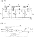
- FIG. 2A shows the snubber circuit 3 of FIG. 1 , wherein disposition of each elements in the circuit diagram is changed.
- the snubber circuit 3 shown in FIG. 2A is equivalent to the snubber circuit 3 shown in FIG. 1 .
- the snubber circuit 3 is electrically connected to a pair of first voltage points P11 and P12 of the main circuit 2 and a pair of second voltage points P21 and P22 of the main circuit 2. That is, the main circuit 2 includes the pair of first voltage points P11 and P12 and the pair of second voltage points P21 and P22 electrically connected to the snubber circuit 3.
- the pair of first voltage points P11 and P12 is directly connected to the pair of bus voltage points P1 and P2.
- the pair of second voltage points P21 and P22 is directly connected to the pair of bus voltage points P1 and P2.
- the first voltage point P11 on the high-potential side, the second voltage point P21, and the bus voltage point P1 are electrically equivalent points at the same potential.
- the first voltage point P12 on the low-potential side, the second voltage point P22, and the bus voltage point P2 are electrically equivalent points at the same potential.
- the pair of first voltage points P11 and P12 and the pair of second voltage points P21 and P22 are each denoted by a terminal symbol for circuit diagram in FIG. 2A but do not necessarily have to be components (terminals) for connecting electric wires and the like.
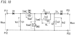
- the snubber circuit 3 includes a first clamp circuit 31, a second clamp circuit 32, a voltage conversion circuit 33, and a control circuit 34 (see FIG. 2B ).
- the first clamp circuit 31 is a circuit configured to, when the magnitude of the voltage (bus voltage Vbus) between the pair of first voltage points P11 and P12 in the main circuit 2 exceeds a first clamp value v1 (see FIG. 3B ), absorb electrical energy of the main circuit 2 from the pair of first voltage points P11 and P12. Thus, the first clamp circuit 31 clamps the voltage between the pair of first voltage points P11 and P12 to the first clamp value v1. That is, when the bus voltage Vbus of the main circuit 2 exceeds the first clamp value v1, the first clamp circuit 31 extracts, from the main circuit 2, electrical energy exceeding the first clamp value v1, thereby clamping an upper limit value of the bus voltage Vbus to the first clamp value v1.
- the first clamp circuit 31 includes a first diode D1 and a first capacitive element C1 (capacitor).
- the first diode D1 and the first capacitive element C1 are electrically connected in series between the pair of first voltage points P11 and P12.
- the first clamp circuit 31 is configured to, when the voltage (bus voltage Vbus) between the pair of first voltage points P11 and P12 exceeds the first clamp value v1, cause a current Id1 to flow from the main circuit 2 through the first diode D1 to the first capacitive element C1.
- the first diode D1 has an anode electrically connected to the first voltage point P11 on the high-potential side.
- the first diode D1 has a cathode electrically connected via the first capacitive element C1 to the first voltage point P12 on the low-potential side.
- the forward direction drop voltage of the first diode D1 is sufficiently smaller than the first clamp value v1, and therefore, the present embodiment is described assuming that the forward direction drop voltage of the first diode D1 is zero, that is, the magnitude of the voltage across the first capacitive element C1 corresponds to the first clamp value v1.
- the second clamp circuit 32 is a circuit configured to, when the magnitude of the voltage (bus voltage Vbus) between the pair of second voltage points P21 and P22 in the main circuit 2 falls below a second clamp value v2 (see FIG. 3 ), inject electrical energy to the main circuit 2 from the pair of second voltage points P21 and P22.
- the second clamp circuit 32 clamps the voltage between the pair of second voltage points P21 and P22 to the second clamp value v2. That is, when the bus voltage Vbus of the main circuit 2 falls below the second clamp value v2, the second clamp circuit 32 regenerates electrical energy corresponding to a difference between the bus voltage Vbus and the second clamp value v2 in the main circuit 2, thereby clamping a lower limit value of the bus voltage Vbus to the second clamp value v2.
- the second clamp circuit 32 includes a second diode D2 and a second capacitive element C2 (capacitor).
- the second diode D2 and the second capacitive element C2 are electrically connected in series between the pair of second voltage points P21 and P22.
- the second clamp circuit 32 is configured to, when the voltage (bus voltage Vbus) between the pair of second voltage points P21 and P22 falls below the second clamp value v2, cause a current Id2 to flow from the second capacitive element C2 through the second diode D2 to the main circuit 2.
- the second diode D2 has a cathode electrically connected to the second voltage point P21 on the high-potential side.
- the second diode D2 has an anode electrically connected via the second capacitive element C2 to the second voltage point P22 on the low-potential side.
- the forward direction drop voltage of the second diode D2 is sufficiently smaller than the second clamp value v2, and therefore, the present embodiment is described assuming that the forward direction drop voltage of the second diode D2 is zero, that is, the magnitude of the voltage across the second capacitive element C2 corresponds to the second clamp value v2.
- the voltage conversion circuit 33 is electrically connected to the first clamp circuit 31 and the second clamp circuit 32.
- the voltage conversion circuit 33 performs voltage conversion (step-down, step-up, or step-up and down) between a first clamp voltage Vc1 and a second clamp voltage Vc2.
- first clamp voltage is a voltage defining the first clamp value v1 and is, in the present embodiment, the voltage across the first capacitive element C1.
- second clamp voltage is a voltage defining the second clamp value v2 and is, in the present embodiment, the voltage across the second capacitive element C2.
- the voltage conversion circuit 33 is a chopper-type DC/DC converter including a first switch SW1 as a semiconductor switch and an inductor L1.
- the voltage conversion circuit 33 is a step-down (chopper) circuit and steps down the first clamp voltage Vc1 to generate the second clamp voltage Vc2. That is, the voltage conversion circuit 33 steps down the voltage across the first capacitive element C1 to generate the voltage across the second capacitive element C2.
- the voltage conversion circuit 33 includes a second switch SW2 and a capacitive element C3 (capacitor) in addition to the first switch SW1 and the inductor L1.
- each of the first switch SW1 and the second switch SW2 is an n-channel depletion MOSFET.
- the first switch SW1 and the second switch SW2 are electrically connected in series between both ends of the first capacitive element C1.
- the drain of the first switch SW1 is electrically connected to the cathode of the first diode D1 of the first clamp circuit 31.
- the source of the second switch SW2 is electrically connected to the negative electrode-side terminal (the first voltage point P12) of the first capacitive element C1.
- the inductor L1 is electrically connected in series to the second switch SW2 between both ends of the second capacitive element C2. In other words, the inductor L1 is electrically connected between a connection point of the source of the first switch SW1 and the drain of the second switch SW2 and the anode of the second diode D2 of the second clamp circuit 32.
- the capacitive element C3 is electrically connected in parallel to the inductor L1 between a connection point of the source of the first switch SW1 and the drain of the second switch SW2 and the anode of the second diode D2 of the second clamp circuit 32.
- the capacitive element C3 is provided to realize soft switching of the first switch SW1 and the second switch SW2, which will be described later in detail in "(3.3) soft switching".
- the control circuit 34 outputs control signals S1 and S2 for respectively controlling the first switch SW1 and the second switch SW2.
- the control signals S1 and S2 are respectively applied to the gate of the first switch SW1 and the gate of the second switch SW2 directly or via a drive circuit to individually turn on/off the first switch SW1 and the second switch SW2.
- the control circuit 34 controls the first switch SW1 and the second switch SW2 based on the PWM system which enables the duty ratio to be adjusted.
- the control circuit 34 is an autonomous control circuit which performs feedback control by using an analog circuit.
- the control circuit 34 includes, for example, an FPGA or an ASIC.
- the control circuit 34 determines the duty ratios of the control signals S1 and S2 based on the first clamp voltage Vc1 (the voltage across the first capacitive element C1) and the average value of the voltage (bus voltage Vbus) between the pair of second voltage points P21 and P22. That is, the control circuit 34 detects the first clamp voltage Vc1 and the bus voltage Vbus and inputs, to a comparator, a sawtooth wave and a value obtained by multiplying, by a coefficient (k3), a difference between values obtained by multiplying the first clamp voltage Vc1 and the bus voltage Vbus respectively by coefficients (k1, k2), thereby generating the control signals S1 and S2.
- control signal S1 and the control signal S2 are signals whose waveforms are inverted so that the first switch SW1 and the second switch SW2 are alternately turned on.
- the step-down ratio of the voltage conversion circuit 33 changes, which will also be described in detail in "(3.2) Operation of Snubber Circuit".
- the first clamp value v1 is automatically determined relative to an average value v0 (see FIG. 3B ) of the bus voltage Vbus.
- the power conversion system 1 is, as described above, configured to bidirectionally convert electric power between the pair of primary-side terminals T11 and T12 and the pair of secondary-side terminals T21 and T22 via the transformer 26.
- the main circuit 2 has two operation modes, namely an "inverter mode” and a "converter mode".
- the inverter mode is an operation mode in which the direct-current power input to the pair of primary-side terminals T11 and T12 is converted into the alternating-current power to output the alternating-current power from the pair of secondary-side terminals T21 and T22.
- the converter mode is an operation mode in which the alternating-current power input to the pair of secondary-side terminals T21 and T22 is converted into the direct-current power to output the direct-current power from the pair of primary-side terminals T11 and T12.
- the main control circuit 25 controls the first to fourth switching elements Q11 to Q14 of the first converter 21 such that a combination of the first and third switching elements Q11 and Q13 and a combination of the second and fourth switching elements Q12 and Q14 are alternately turned on.
- the duty ratio of each of the first and third switching elements Q11 and Q13 (or second and fourth switching elements Q12 and Q14) is 50%.
- the pair of bus voltage points P1 and P2 alternately receives the voltage E from the winding wire L21 and the winding wire L22.
- the main control circuit 25 performs PWM control of the second converter 22, thereby controlling the output voltage of the second converter 22. Specifically, during a supply time period during which the fifth and eighth switching elements Q15 and Q18 (or sixth and seventh switching elements Q16 and Q17) are ON, a current is supplied from the winding wire L22 (or winding wire L21) through the second converter 22 to the pair of secondary-side terminals T21 and T22. On the other hand, during a circulation time period during which the fifth and seventh switching elements Q15 and Q17 (or sixth and eighth switching elements Q16 and Q18) are ON, a current from the inductor L10 flows through the second converter 22 as a return path. The main control circuit 25 changes a ratio of the supply time period to the circulation time period, thereby controlling the output voltage of the second converter 22. Inversion operation in the secondary winding wire 262 of the transformer 26 of the first converter 21 is performed during the circulation time period.
- the main circuit 2 repeats the operation described above to convert direct-current power from the storage battery 5 into alternating-current power and outputs the alternating-current power from the pair of secondary-side terminals T21 and T22 to the power system 4.
- the main circuit 2 causes the first converter 21 and the second converter 22 to operate also in the converter mode based on a sequence basically similar to that in the inverter mode. That is, in the main circuit 2, when the output voltage of the second converter 22 is lower than the voltage of the power system 4, the alternating-current power from the power system 4 is converted into the direct-current power, which is output from the pair of primary-side terminals T11 and T12 to the storage battery 5.
- ringing may be caused in the bus voltage Vbus, which is a direct-current voltage, generated at the pair of bus voltage points P1 and P2. That is, since the second converter 22 is connected via the transformer 26 to the storage battery 5 serving as a direct-current power supply, the second converter 22 may be deemed to be electrically connected via leakage inductance of the transformer 26 to the direct-current power supply (storage battery 5). Thus, when switching operation of the second converter 22 is performed, ringing may occur in the bus voltage Vbus.
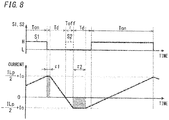
- the bus voltage Vbus is shown with the horizontal axis being a time axis.
- the bus voltage Vbus is shown in a graph in an upper section, and the currents Id1 and Id2 (see FIG. 2A ) are shown in a graph in a lower section, where the horizontal axis is a time axis.
- the current Id1 represents a current flowing through the first diode D1 of the snubber circuit 3
- the current Id2 represents a current flowing through the second diode D2 of the snubber circuit 3.
- the bus voltage Vbus before being clamped is indicated by a broken line.
- the current Id1 is indicated by a broken line
- the current Id2 is represented by a solid line.
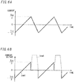
- positive ringing and negative ringing may occur in the bus voltage Vbus, which is a direct-current voltage, generated at the pair of bus voltage points P1 and P2.
- the term "positive ringing” means ringing in a direction (positive direction) in which the voltage increases (to "vr1” in FIG. 3A ) with respect to the average value v0 of the bus voltage Vbus.
- the term “negative ringing” means ringing in a direction (negative direction) in which the voltage decreases (to "vr2" in FIG. 3A ) with respect to the average value v0 of the bus voltage Vbus.
- the snubber circuit 3 absorbs electrical energy of the main circuit 2 by using the first clamp circuit 31 to clamp the bus voltage Vbus to the first clamp value v1 as illustrated in FIG. 3B . That is, when as a result of the occurrence of the positive ringing in the bus voltage Vbus, the magnitude of the bus voltage Vbus exceeds the first clamp value v1, the first diode D1 is turned on, and the first clamp circuit 31 operates. At this time, as illustrated in FIG. 3B , as the electrical energy is absorbed by the first clamp circuit 31, the current Id1 having a pulse shape flows through the first diode D1.
- the snubber circuit 3 performs voltage conversion between the first clamp voltage Vc1 and the second clamp voltage Vc2 by using the voltage conversion circuit 33 electrically connected between the first clamp circuit 31 and the second clamp circuit 32.
- the voltage conversion circuit 33 alternately turns on the first switch SW1 and the second switch SW2 based on the control signals S1 and S2 from the control circuit 34 to step-down the first clamp voltage Vc1, thereby generating the second clamp voltage Vc2.
- the value (second clamp value v2) of the voltage across the second capacitive element C2 as the second clamp voltage Vc2 is smaller than the value (first clamp value v1) of the voltage across the first capacitive element C1 as the first clamp voltage Vc1.
- the snubber circuit 3 injects electrical energy to the main circuit 2 by using the second clamp circuit 32 to clamp the bus voltage Vbus to the second clamp value v2 as illustrated in FIG. 3B . That is, when as a result of the occurrence of the negative ringing in the bus voltage Vbus, the magnitude of the bus voltage Vbus falls below the second clamp value v2, the second diode D2 is turned on, and the second clamp circuit 32 operates. At this time, as illustrated in FIG. 3B , as the electrical energy is injected by the second clamp circuit 32, the current Id2 having a pulse shape flows through the second diode D2.
- the snubber circuit 3 enables electrical energy corresponding to a difference between the bus voltage Vbus and the second clamp value v2 to be regenerated from the second capacitive element C2 in the main circuit 2.
- the minimum value of the bus voltage Vbus is suppressed to the second clamp value v2.
- the electrical energy accumulated in the second capacitive element C2 is electrical energy provided via the voltage conversion circuit 33 from the first capacitive element C1. That is, the snubber circuit 3 regenerates electrical energy absorbed from the main circuit 2 by using the first clamp circuit 31 at the occurrence of the positive ringing in the bus voltage Vbus from the second clamp circuit 32 in the main circuit 2 at the occurrence of the negative ringing in the bus voltage Vbus. Moreover, in other words, in the snubber circuit 3, the electrical energy absorbed at the occurrence of the positive ringing is stored once and is regenerated at the occurrence of the negative ringing. In this way, the electrical energy of the positive ringing which occurs in the bus voltage Vbus and the electrical energy of the negative ringing are canceled out each other, thereby reducing both the positive ringing and the negative ringing in the bus voltage Vbus.
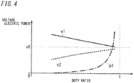
- adjusting the duty ratio of the control signal S1 for controlling the first switch SW1 enables the first clamp value v1 and the second clamp value v2 to be adjusted. That is, when the duty ratio of the control signal S1 changes, the step-down ratio of the voltage conversion circuit 33 changes, and therefore, along with this change, the first clamp value v1 and the second clamp value v2 also change.
- FIG. 4 is a graph showing a relationship of the duty ratio to the first clamp value v1 and the second clamp value v2 with the horizontal axis representing the duty ratio of the control signal S1. Moreover, FIG. 4 also shows a relationship between the duty ratio and the electric power regenerated by the snubber circuit 3 in the main circuit 2 (hereinafter referred to as a "regenerated electric power p1").
- the duty ratio of the control signal S1 increases, that is, the ratio of the ON time period of the first switch SW1 in the switching cycle of the first switch SW1 increases, the first clamp value v1 decreases, and the second clamp value v2 increases.
- the duty ratio of the control signal S1 approaches the maximum value "1”
- the first clamp value v1 and the second clamp value v2 approaches the average value v0 of the bus voltage Vbus.
- the first clamp value v1 does not fall below the average value v0 of the bus voltage Vbus
- the second clamp value v2 does not exceed the average value v0 of the bus voltage Vbus.
- the regenerated electric power p1 increases.
- the duty ratio of the control signal S1 decreases, that is, the ratio of the ON time period of the first switch SW1 in the switching cycle of the first switch SW1 decreases, the first clamp value v1 increases, and the second clamp value v2 decreases.
- the duty ratio of the control signal S1 decreases, the regenerated electric power p1 decreases.
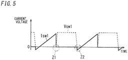
- FIG. 5 shows a voltage across the first switch SW1 (hereinafter referred to as a "switch voltage Vswl”) and a current flowing through the first switch SW1 (hereinafter referred to as a "switch current Iswl”) with the horizontal axis being a time axis.
- the first condition is that as an area Z2 shown in FIG. 5 , at a timing of turning on the first switch SW1 (switching from an OFF state to an ON state), a current flowing through the inductor L1 (hereinafter referred to as an "inductor current IL"), that is, the switch current Isw1 falls to or below zero.
- the first condition is that the first switch SW1 performs switching operation such that the inductor current IL of the voltage conversion circuit 33 in the snubber circuit 3 flows according to the discontinuous mode.
- the inductor current IL flows through the inductor L1 discontinuously according to the discontinuous mode.
- the first condition is realized by setting the circuit constant (inductance) of the inductor L1, which will be described later in detail.
- the second condition is that as the area Z1 shown in FIG. 5 , a rise of the switch current Isw1 does not intersect a rise of the switch voltage Vswl.
- the second condition is that at a timing of turning off the first switch SW1 in the snubber circuit 3 (at a timing of switching from the ON state to the OFF state), the switch voltage Vswl does not rise while the switch current Isw1 is falling.
- the second condition is realized by setting the circuit constant (inductance) of the inductor L1 and the circuit constant (capacitance value) of the capacitive element C3 electrically connected in parallel to the inductor L1, which will be described later in detail.
- Vin is the voltage across the first capacitive element C1 (i.e., first clamp value v1)
- Vo is the voltage across the second capacitive element C2 (i.e., second clamp value v2)
- L is the inductance of the inductor L1.
- Ton T ⁇ Vo Vin ⁇ ⁇ 2
- a negative peak value of the inductor current IL that is, a minimum value Imin of the inductor current IL in a case of a load current Io flowing to the snubber circuit 3 is obtained.
- the term "load current Io" means an output current of the snubber circuit 3, that is, the current Id2 flowing through the second diode D2.
- the inductor current IL increases by the load current Io.
- FIG. 7B shows the switch current Isw1 and the switch voltage Vswl in this case.
- the minimum value Imin of the inductor current IL is expressed by a value obtained by subtracting ILp/2 from the load current Io and is expressed by the expressions [Formula 4] below.
- Imin Io ⁇ Vin ⁇ Vo 2 ⁇ L TVo Vin ⁇ ⁇ 2
- the minimum value Imin of the inductor current IL has to be less than zero.
- the inductance L of the inductor L1 has to satisfy the expression [Formula 5] below obtained by solving L of the expression [Formula 4]. That is, if the inductance L of the inductor L1 is set within a range satisfying the condition defined by the expression [Formula 5], the first condition is satisfied.
- the load current Io is variable, the load current Io in the expression [Formula 5] is substituted with a rated value (maximum value) of the load current Io. L ⁇ Vin ⁇ Vo 2 ⁇ Io TVo Vin ⁇ ⁇ 2
- the capacitive element C3 is an element for adjusting an inversion time of the inductor current IL. As illustrated in FIG. 8 , the capacitive element C3 is electrically connected in parallel to the inductor L1, thereby functioning to delay an inversion timing of the inductor current IL, that is, a start of rising of the inductor current IL.
- the first switch SW1 when the first switch SW1 is turned on, it is possible to control the inductor current IL to be zero or less, so that soft switching of the first switch SW1 is realizable.
- control signal S1 for controlling the first switch SW1 and the control signal S2 for controlling the second switch SW2 are shown in an upper section, and the inductor current IL is shown in a lower section, where the horizontal axis is a time axis.
- the control signal S1 is "H” (at a high level)
- the first switch SW1 is ON
- the control signal S1 is "L” (at a low level)
- the first switch SW1 is OFF.
- control signal S2 is "H”
- the second switch SW2 is ON
- control signal S2 is "L”
- C is a capacitance value of the capacitive element C3, and D is the duty ratio of the first switch SW1.
- DT in the expressions is a value obtained by adding a dead time Td to an on time Ton, and DT- ⁇ 2 corresponds to a time period during which the inductor current IL increases.
- inversion of the inductor current IL has to be completed within the dead time Td. That is, in the expressions [Formula 6] and [Formula 7], the inductance L of the inductor L1 and the capacitance value C of the capacitive element C3 have to be set such that the relationships ⁇ 1 ⁇ Td and ⁇ 2 ⁇ Td are satisfied.
- the inductance L and the capacitance value C are set within a range satisfying the conditions ⁇ 1 ⁇ Td and ⁇ 2 ⁇ Td in the expressions [Formula 6] and [Formula 7], the second condition is satisfied.
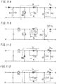
- FIGS. 9 to 12C show an operation sequence of the snubber circuit 3 in further detail with reference to FIGS. 9 to 12C .
- a voltage and a current of each component in the snubber circuit 3 are defined as indicated by arrows in FIG. 10 .
- the (positive/negative) polarity of the voltage or the current is also defined such that the direction indicated by the arrow in FIG. 10 is the "positive" direction of the voltage or the current.
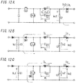
- FIGS. 11A to 12C shows an equivalent circuit reflecting the operation of the snubber circuit 3 in a corresponding one of phases so as to describe the operation of the snubber circuit 3.
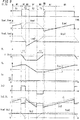
- the operation of the snubber circuit 3 is divided into seven phases, namely a first phase M1 to a seventh phase M7.
- the horizontal axis is a time axis
- the control signal S1 and the control signal S2 are shown in the uppermost section
- the switch current Isw1 and the switch voltage Vswl are shown in the second section
- a switch current Isw2 and a switch voltage Vsw2 are shown in the third section.
- a voltage across the inductor L1 (hereinafter referred to as an "inductor voltage VL") is shown in the fourth section, the inductor current IL is shown in the fifth section, the load current Io is shown in the sixth section, and a current Ic3 flowing through a third capacitive element C3 is shown in the seventh section. Furthermore, a current Ic2 and the inductor current IL flowing through the second capacitive element C2 are shown in the eighth section, and the second clamp voltage Vc2 and the switch voltage Vsw2 are shown in the lowermost section.
- control signal S1 and the control signal S2 have asymmetrical signal waveforms and the duty ratios of the control signals S1 and S2 are fixed values so that the on time length of the first switch SW1 is different from the on time length of the second switch SW2.
- the snubber circuit 3 is equivalently in an operational state as illustrated in FIG. 11A .
- the inductor voltage VL is a constant voltage to maintain a difference value (v1-v2) between the first clamp value v1 and the second clamp value v2.
- the inductor current IL linearly increases.
- the switch current Isw1 at this time is equal to the inductor current IL.
- the first switch SW1 is turned off, and the second switch SW2 remains in the OFF state, thereby transitioning to the dead time Td.
- the snubber circuit 3 is equivalently in the operational state as illustrated in FIG. 11B .
- the inductor L1 and the third capacitive element C3 are electrically disconnected from the pair of first voltage points P11 and P12 and the pair of second voltage points P21 and P22 to configure an LC parallel resonance circuit.
- the third capacitive element C3 is discharged, and thereby, the current Ic3 flows in a direction indicated by the arrow in FIG. 11B , and the orientation (polarity) of the inductor voltage VL is gradually inverted.
- the current Ic3 is equal to the inductor current IL, and the load current Io is equal to the current Ic2.
- the third capacitive element C3 delays a rise of the switch voltage Vsw1 to avoid overlapping of the switch voltage Vsw1 and the switch current Isw1, so that soft switching is realized.
- the third phase M3 corresponds to the dead time Td after the inversion of the orientation (polarity) of the inductor voltage VL, the first switch SW1 remains in the OFF state, the second switch SW2 remains in the OFF state, and the snubber circuit 3 is equivalently in the operational state as illustrated in FIG. 11C .
- a parasitic diode of the second switch SW2 is turned on, and through the parasitic diode, a return current flows in a direction indicated by the arrow in FIG. 11C .
- the inductor voltage VL is a constant voltage and maintains the same value as the second clamp voltage Vc2.
- the third capacitive element C3 is neither charged nor discharged.
- the switch voltage Vsw1 rises to the maximum value (first clamp value v1).
- the snubber circuit 3 is equivalently in an operational state as illustrated in FIG. 11D .
- a return current flows through the second switch SW2 for a while.
- the polarities of the switch current Isw2, the inductor current IL, and the current Ic2 are inverted. That is, the switch current Isw2 changes from a negative current to a positive current, the inductor current IL changes from a positive current to a negative current, and the current Ic2 changes from a positive current to a negative current.
- the inductor current IL changes to a negative current, discharging of the second capacitive element C2 is started.
- the first switch SW1 remains in the OFF state, and the second switch SW2 is turned off, thereby transitioning to the dead time Td.
- the snubber circuit 3 is equivalently in the operational state as illustrated in FIG. 12A .
- the inductor L1 and the third capacitive element C3 are electrically disconnected from the pair of first voltage points P11 and P12 and the pair of second voltage points P21 and P22 to configure an LC parallel resonance circuit.
- the third capacitive element C3 is discharged, and thereby, the current Ic3 flows in a direction indicated by the arrow in FIG. 12A , and the orientation (polarity) of the inductor voltage VL is gradually inverted.
- the current Ic3 is equal to the inductor current IL
- the load current Io is equal to the current Ic2.
- the sixth phase M6 corresponds to the dead time Td after the inversion of the direction (polarity) of the inductor voltage VL, the first switch SW1 remains in the OFF state, the second switch SW2 remains in the OFF state, and the snubber circuit 3 is equivalently in the operational state as illustrated in FIG. 12B .
- a parasitic diode of the first switch SW1 is turned on, and through the parasitic diode, the inductor current IL is regenerated in the first capacitive element C1.
- the snubber circuit 3 is equivalently in an operational state as illustrated in FIG. 12C .
- the switch current Isw1 is equal to the inductor current IL, but subsequently to the sixth phase M6, the inductor current IL is regenerated in the first capacitive element C1.
- the polarity of the switch current Isw1 is negative, and the parasitic diode of the first switch SW1 is conductive when the switch voltage Vswl falls, and therefore, switching loss is reduced.
- the power storage system including the power conversion system 1 and the storage battery 5 is not limited to the use in non-dwelling facilities but may be introduced into, for example, dwelling houses or may be applied to objects such as an electric vehicle other than facilities.
- the power conversion system 1 is not limited to the use for electric power conversion between the power system 4 and the storage battery 5 but may be used for electric power conversion between a power generating facility such as a photovoltaic generator or a fuel cell and a power system 4 or a load.
- the power conversion system 1 is not limited to a configuration for bidirectionally converting electric power but may be configured to only unidirectionally convert electric power, for example, from the pair of primary-side terminals T11 and T12 to the pair of secondary-side terminals T21 and T22.
- the second switch SW2 is not limited to the MOSFET but may be, for example, a diode.
- the second switch SW2 is provided in the same direction as a parasitic diode of the MOSFET, that is, is connected such that the cathode is connected to the source of the first switch SW1 and the anode is connected to the first voltage point P12 on the low-potential side.
- the second clamp circuit 32 may regenerate electrical energy absorbed from the pair of first voltage points P11 and P12 of the main circuit 2 by the first clamp circuit 31 from a location electrically different from the pair of first voltage points P11 and P12 in the main circuit 2.
- the voltage conversion circuit 33 is not limited to the step-down circuit configured to step-down the first clamp voltage Vc1 to generate the second clamp voltage Vc2 but may be, for example, a step-up circuit configured to step-up the first clamp voltage Vc1 to generate the second clamp voltage Vc2.
- the capacitive element C3 is electrically connected in parallel to the inductor L1, but it is required only that the capacitive element C3 is electrically connected in parallel at least to one of the first switch SW1 and the inductor L1. That is, the capacitive element C3 may be electrically connected in parallel to the first switch SW1 or may be electrically connected in parallel to both the first switch SW1 and the inductor L1.
- the first diode D1 is not limited to the configuration as described in the embodiment in which the first diode D1 is electrically connected to the first voltage point P11 of the pair of first voltage points P11 and P12 which is located on the high-potential side.
- the first diode D1 may be electrically connected to the first voltage point P12 on the low-potential side.
- the second diode D2 may be electrically connected to the second voltage point P22 of the pair of second voltage points P21 and P22 which is located on the low-potential side.
- the first diode D1 and the second diode D2 may be, for example, parasitic diodes of a MOSFET.
- each of the first to eighth switching elements Q11 to Q18 includes a parasitic diode of a MOSFET, but separately from the parasitic diode, a diode may be electrically connected antiparallel to each of the first to eighth switching elements Q11 to Q18.
- each of the first to eighth switching elements Q11 to Q18 is not limited to a MOSFET but may be, for example, an Insulated Gate Bipolar Transistor (IGBT).
- IGBT Insulated Gate Bipolar Transistor
- the RC snubber 23 is not a component essential for the power conversion system 1 (main circuit 2). Thus, the RC snubber 23 may accordingly be omitted.
- the first clamp voltage Vc1 is at least a voltage defining the first clamp value v1, it is not essential that the magnitude of the first clamp voltage Vc1 corresponds to the first clamp value v1, and for example, the magnitude of the voltage obtained by dividing the first clamp voltage Vc1 may correspond to the first clamp value v1.
- the second clamp voltage Vc2 is at least a voltage defining the second clamp value v2.
- the power system 4 corresponds to single-phase electric power has been described, but this should not be construed as limiting.
- the power system 4 may correspond to, for example, three-phase electric power.
- the main circuit 2 preferably includes three primary-side terminals and three secondary-side terminals.
- a snubber circuit 3 of a first aspect includes a first clamp circuit 31, a second clamp circuit 32, and a voltage conversion circuit 33.
- the first clamp circuit 31 is configured to, when a magnitude of a voltage between a pair of first voltage points P11 and P12 in a main circuit 2 exceeds a first clamp value v1, absorb electrical energy of the main circuit 2 from the pair of first voltage points P11 and P12. Thus, the first clamp circuit 31 clamps the voltage between the pair of first voltage points P11 and P12 to the first clamp value v1.
- the second clamp circuit 32 is configured to, when a magnitude of a voltage between a pair of second voltage points P21 and P22 in the main circuit 2 falls below a second clamp value v2, inject electrical energy to the main circuit 2 from the pair of second voltage points P21 and P22. Thus, the second clamp circuit 32 clamps the voltage between the pair of second voltage points P21 and P22 to the second clamp value v2.
- the voltage conversion circuit 33 is electrically connected to the first clamp circuit 31 and the second clamp circuit 32 and is configured to perform voltage conversion between a first clamp voltage Vc1 and a second clamp voltage Vc2.
- the first clamp voltage Vc1 defines the first clamp value v1.
- the second clamp voltage Vc2 defines the second clamp value v2.
- the snubber circuit 3 absorbs electrical energy of the main circuit 2 by using the first clamp circuit 31 to clamp the bus voltage Vbus to the first clamp value v1.
- the snubber circuit 3 injects electrical energy to the main circuit 2 by using the second clamp circuit 32 to clamp the bus voltage Vbus to the second clamp value v2.
- the voltage conversion circuit 33 performs voltage conversion between the first clamp voltage Vc1 defining the first clamp value v1 and the second clamp voltage Vc2 defining the second clamp value v2.
- the snubber circuit 3 regenerates electrical energy absorbed from the main circuit 2 by using the first clamp circuit 31 at the occurrence of the positive ringing from the second clamp circuit 32 in the main circuit 2 at the occurrence of the negative ringing.
- the snubber circuit 3 more effectively uses electrical energy than an RCD snubber circuit configured to convert absorbed energy into heat for consumption, and thus, it is possible to suppress loss at the snubber circuit 3 to a low level.
- the snubber circuit 3 regenerates electrical energy only when the voltage between the pair of first voltage points P11 and P12 exceeds the first clamp value v1 and when the voltage between the pair of second voltage points P21 and P22 falls below the second clamp value v2.
- the snubber circuit 3 enables only a ringing component to be regenerated without regeneration of a normal voltage (bus voltage Vbus) applied between the pair of first voltage points P11 and P12 or between the pair of second voltage points P21 and P22.
- the snubber circuit 3 enables influence over operation of the main circuit 2 to be suppressed to a relatively low level.
- the snubber circuit 3 does not have to have a transformer, so that simplification of the configuration and a reduction of loss of the snubber circuit 3 are possible.
- an autonomous control circuit 34 is adopted for controlling the voltage conversion circuit 33, it is possible to suppress the circuit dimension of the snubber circuit 3 to a small dimension.
- the first voltage point P11 of the pair of first voltage points P11 and P12 is located on a high-potential side
- the second voltage point P21 of the pair of second voltage points P21 and P22 is located on the high-potential side
- a potential at the first voltage point P11 is preferably equal to a potential at the second voltage point P21.
- the first voltage point P12 of the pair of first voltage points P11 and P12 is located on a low-potential side
- the second voltage point P22 of the pair of second voltage points P21 and P22 is located on the low-potential side
- a potential at the first voltage point P12 is preferably equal to a potential at the second voltage point P22.
- the voltage conversion circuit 33 is preferably configured to step down the first clamp voltage Vc1 to generate the second clamp voltage Vc2. This configuration enables the second clamp circuit 32 to regenerate electrical energy absorbed from the pair of first voltage points P11 and P12 of the main circuit 2 by the first clamp circuit 31 from a location electrically equivalent to the pair of first voltage points P11 and P12 in the main circuit 2.
- the snubber circuit 3 is applicable to the main circuit 2 configured to bidirectionally convert electric power.
- the voltage conversion circuit 33 is preferably a DC/DC converter including a semiconductor switch (first switch SW1), an inductor L1, and a capacitive element C3.
- the capacitive element C3 is preferably electrically connected in parallel to at least one of the semiconductor switch and the inductor L1. This configuration enables soft switching of a semiconductor switch in the voltage conversion circuit 33 to be realized and ringing and loss occurring in the snubber circuit 3 to be suppressed to a low level. Note that this configuration is not an essential configuration of the snubber circuit 3, and the capacitive element C3 may accordingly be omitted.
- the first clamp circuit 31 preferably includes a first diode D1 and a first capacitive element C1 which are electrically connected in series between the pair of first voltage points P11 and P 12.
- the first clamp circuit 31 is preferably configured to, when the voltage between the pair of first voltage points P11 and P12 exceeds the first clamp value v1, cause a current to flow from the main circuit 2 through the first diode D1 to the first capacitive element C1.
- the second clamp circuit 32 includes a second diode D2 and a second capacitive element C2 which are electrically connected in series between the pair of second voltage points P21 and P22.
- the second clamp circuit 32 is preferably configured to, when the voltage between the pair of second voltage points P21 and P22 falls below the second clamp value v2, cause a current to flow from the second capacitive element C2 through the second diode D2 to the main circuit 2.
- a relatively simple circuit configuration including a diode and a capacitive element (capacitor, or the like) realizes the first clamp circuit 31 and the second clamp circuit 32.
- the voltage conversion circuit 33 is preferably a DC/DC converter including a semiconductor switch (first switch SW1) and an inductor L1.
- the voltage conversion circuit 33 is preferably configured to cause the semiconductor switch to perform switching operation such that an inductor current IL flowing through the inductor L1 is in a discontinuous mode.
- This configuration enables soft switching of a semiconductor switch in the voltage conversion circuit 33 to be realized and ringing and loss occurring in the snubber circuit 3 to be suppressed to a low level. Note that this configuration is not an essential configuration of the snubber circuit 3, and the voltage conversion circuit 33 may cause a semiconductor switch to perform switching operation such that the inductor current IL flowing through the inductor L1 is in a critical mode or a continuous mode.
- the voltage conversion circuit 33 is preferably a DC/DC converter including a semiconductor switch (first switch SW1), an inductor L1, and a control circuit 34 configured to control the semiconductor switch.
- the control circuit 34 is preferably configured to adjust a duty ratio of the semiconductor switch to adjust the first clamp value v1 and the second clamp value v2. With this configuration, adjusting the duty ratio of the semiconductor switch enables the first clamp value v1 and the second clamp value v2 to be set to arbitrary values. Note that this configuration is not an essential configuration of the snubber circuit 3, and the duty ratio of the semiconductor switch may be fixed.
- a power conversion system 1 of a seventh aspect includes the snubber circuit 3 of any one of the first to sixth aspects, and a main circuit 2, wherein the main circuit 2 is a power conversion circuit configured to convert electric power.
- the snubber circuit 3 more effectively uses electrical energy than an RCD snubber circuit, and thus, it is possible to suppress loss at the snubber circuit 3 to a low level.
- the loss in the snubber circuit 3 in the power conversion system 1 is reduced to a low level, and as the entirety of the power conversion system 1, it is possible to improve the conversion efficiency of the electric power.
- the main circuit 2 performs electric power conversion of relatively large electric power, heat generation by the snubber circuit 3 is reduced, which also leads to downsizing and simplification of the heat dissipation structure of the snubber circuit 3.
- the main circuit 2 preferably includes two or more primary-side terminals T11 and T12, two or more secondary-side terminals T21 and T22, and a high-frequency insulated transformer (transformer 26).
- the main circuit 2 is preferably configured to convert electric power between a set of the two or more primary-side terminals T11 and T12 and a set of the two or more secondary-side terminals T21 and T22 via the high-frequency insulated transformer.
- the power conversion system 1 may adopt an insulating-type circuit configuration.
- the snubber circuit 3 is preferably electrically connected to the high-frequency insulated transformer (transformer 26). With this configuration, ringing occurring due to leakage inductance of the high-frequency insulated transformer can be controlled by the snubber circuit 3.
Abstract

Description
- The present disclosure generally relates to snubber circuits and power conversion systems including the snubber circuits, and specifically to a snubber circuit for suppressing a ringing or surge voltage and a power conversion system including the snubber circuit.
-
Patent Literature 1 describes a snubber circuit used in a power conversion system such as an alternating-current/direct-current power converter. - In
Patent Literature 1, an AC/AC frequency converter connected to a primary side of a high-frequency transformer includes a three-phase rectifier, an inverter, and a snubber circuit. The three-phase rectifier has an input side connected to a three-phase commercial AC power supply and an output side connected to an input side of the inverter. The input side of the inverter is connected to the output side of the three-phase rectifier, and an output side of the inverter is connected to the primary side of the high-frequency transformer. The snubber circuit is connected between the three-phase rectifier and the inverter. - The snubber circuit described in
Patent Literature 1 absorbs, as energy, a spike-like overvoltage caused due to leakage inductance of the high-frequency transformer and regenerates the energy absorbed. The snubber circuit is an RCD single direction snubber circuit of regenerative type including a resistor, a capacitor, a diode, and a semiconductor switch. - In the RCD single direction snubber circuit as described in
Patent Literature 1, at least part of the energy absorbed is converted into heat and consumed by the resistor. Thus, as electric power to be converted by the power conversion system increases, loss in the snubber circuit increases. - Patent Literature 1:
JP 2013-158064 A - In view of the foregoing, it is an object of the present disclosure to provide a snubber circuit configured to suppress loss to a low level and a power conversion system including the snubber circuit.
- A snubber circuit of a first aspect includes a first clamp circuit, a second clamp circuit, and a voltage conversion circuit. The first clamp circuit is configured to, when a magnitude of a voltage between a pair of first voltage points in a main circuit exceeds a first clamp value, absorb electrical energy of the main circuit from the pair of first voltage points. Thus, the first clamp circuit clamps the voltage between the pair of first voltage points to the first clamp value. The second clamp circuit is configured to, when a magnitude of a voltage between a pair of second voltage points in the main circuit falls below a second clamp value, inject electrical energy to the main circuit from the pair of second voltage points. Thus, the second clamp circuit clamps the voltage between the pair of second voltage points to the second clamp value. The voltage conversion circuit is electrically connected to the first clamp circuit and the second clamp circuit and is configured to perform voltage conversion between a first clamp voltage and a second clamp voltage. The first clamp voltage defines the first clamp value. The second clamp voltage defines the second clamp value.
- In a snubber circuit of a second aspect referring to the first aspect, one first voltage point of the pair of first voltage points is located on a high-potential side, one second voltage point of the pair of second voltage points is located on the high-potential side, and a potential at the one first voltage point is equal to a potential at the one second voltage point. In this case, the other first voltage point of the pair of first voltage points is located on a low-potential side, the other second voltage point of the pair of second voltage points is located on the low-potential side, and a potential at the other first voltage point is equal to a potential at the other second voltage point. The voltage conversion circuit is configured to step down the first clamp voltage to generate the second clamp voltage.
- In a snubber circuit of a third aspect referring to the first or second aspect, the voltage conversion circuit is a DC/DC converter including a semiconductor switch, an inductor, and a capacitive element. In this case, the capacitive element is electrically connected in parallel to at least one of the semiconductor switch and the inductor.
- In a snubber circuit of a fourth aspect referring to any one of the first to third aspects, the first clamp circuit includes a first diode and a first capacitive element which are electrically connected in series between the pair of first voltage points. In this case, the first clamp circuit is configured to, when the voltage between the pair of first voltage points exceeds the first clamp value, cause a current to flow from the main circuit through the first diode to the first capacitive element. The second clamp circuit includes a second diode and a second capacitive element which are electrically connected in series between the pair of second voltage points. In this case, the second clamp circuit is configured to, when the voltage between the pair of second voltage points falls below the second clamp value, cause a current to flow from the second capacitive element through the second diode to the main circuit.
- In a snubber circuit of a fifth aspect referring to any one of the first to fourth aspects, the voltage conversion circuit is a DC/DC converter including a semiconductor switch and an inductor. In this case, the voltage conversion circuit is configured to cause the semiconductor switch to perform switching operation such that an inductor current flowing through the inductor is in a discontinuous mode.
- In a snubber circuit of a sixth aspect referring to any one of the first to fifth aspects, the voltage conversion circuit is a DC/DC converter including a semiconductor switch, an inductor, and a control circuit configured to control the semiconductor switch. In this case, the control circuit is configured to adjust a duty ratio of the semiconductor switch to adjust the first clamp value and the second clamp value.
- A power conversion system of a seventh aspect includes the snubber circuit of any one of the first to sixth aspects, and the main circuit. The main circuit being a power conversion circuit configured to convert electric power.
- In a power conversion system of an eighth aspect referring to the seventh aspect, the main circuit includes two or more primary-side terminals, two or more secondary-side terminals, and a high-frequency insulated transformer. In this case, the main circuit is configured to convert electric power between a set of the two or more primary-side terminals and a set of the two or more secondary-side terminals via the high-frequency insulated transformer.
- In a power conversion system of an ninth aspect referring to the eighth aspect, the snubber circuit is electrically connected to the high-frequency insulated transformer.
-
-
FIG. 1 is a circuit diagram illustrating a power conversion system of an embodiment of the present disclosure; -
FIG. 2A is a circuit diagram illustrating a snubber circuit of the embodiment of the present disclosure, andFIG. 2B is a block diagram illustrating a control circuit of the snubber circuit; -
FIG. 3A is a waveform diagram illustrating a bus voltage in a case where the snubber circuit is not provided in the power conversion system, andFIG. 3B is a waveform diagram illustrating a bus voltage and a current in a case where the snubber circuit is provided in the power conversion system; -
FIG. 4 is a characteristic view illustrating a relationship of a duty ratio to a voltage and electric power in a voltage conversion circuit of the snubber circuit; -
FIG. 5 is a waveform diagram illustrating a switch voltage and a switch current of the snubber circuit; -
FIG. 6A is a waveform diagram illustrating an inductor current when the snubber circuit is not loaded, andFIG. 6B is a waveform diagram illustrating the switch voltage and the switch current when the snubber circuit is not loaded; -
FIG. 7A is a waveform diagram illustrating the inductor current of the snubber circuit, andFIG. 7B is a waveform diagram illustrating the switch voltage and the switch current of the snubber circuit; -
FIG. 8 is a timing chart illustrating a control signal and the inductor current of the snubber circuit; -
FIG. 9 is a timing chart illustrating an operation sequence of the snubber circuit; -
FIG. 10 is a circuit diagram illustrating the snubber circuit; -
FIG. 11A is a view illustrating an equivalent circuit in a first phase of the snubber circuit,FIG. 11B is a view illustrating the equivalent circuit in a second phase of the snubber circuit,FIG. 11C is a view illustrating the equivalent circuit in a third phase of the snubber circuit, andFIG. 11D is a view illustrating the equivalent circuit in a fourth phase of the snubber circuit; and -
FIG. 12A is a view illustrating the equivalent circuit in a fifth phase of the snubber circuit,FIG. 12B is a view illustrating the equivalent circuit in a sixth phase of the snubber circuit, andFIG. 12C is a view illustrating the equivalent circuit in a seventh phase of the snubber circuit; - First, a schema of a snubber circuit according to the present embodiment and a power conversion system including the snubber circuit will be described with reference to
FIG. 1 . - A
power conversion system 1 includes amain circuit 2 and asnubber circuit 3. Themain circuit 2 is a power conversion circuit configured to convert electric power. Thesnubber circuit 3 is a protection circuit configured to control a ringing or surge voltage generated by themain circuit 2. When themain circuit 2 converts, for example, direct-current power into alternating-current power or the alternating-current power into the direct-current power, ringing may occur due to leakage inductance of a transformer which will be described later. Thepower conversion system 1 according to the present embodiment enables such ringing to be suppressed by thesnubber circuit 3. Thesnubber circuit 3 corresponds to a sub-circuit with respect to themain circuit 2. - The
power conversion system 1 is used for electric power conversion, for example, between apower system 4 and a storage battery 5 as illustrated inFIG. 1 . As used herein, the term "power system" means an entire system based on which an electricity supplier such as an electric power company supplies electric power to a power receiving facility of a consumer. In the example shown inFIG. 1 , thepower conversion system 1 includes a pair of primary-side terminals T11 and T12 to which the storage battery 5 is electrically connected and a pair of secondary-side terminals T21 and T22 to which thepower system 4 is electrically connected. Thepower conversion system 1 converts alternating-current power input from thepower system 4 into direct-current power and supplies the direct-current power to the storage battery 5 so as to charge the storage battery 5. Thepower conversion system 1 converts direct-current power input from the storage battery 5 into alternating-current power and outputs the alternating-current power to thepower system 4 so as to discharge the storage battery 5. - In the present embodiment, the
power conversion system 1 is configured to bidirectionally convert electric power between the pair of primary-side terminals T11 and T12 and the pair of secondary-side terminals T21 and T22 so as to be compatible with both charging and discharging of the storage battery 5. Thus, thepower conversion system 1 connects and systematically links the storage battery 5 to thepower system 4 to enable the storage battery 5 to be charged with electric power supplied from thepower system 4 and/or to enable a load connected to thepower system 4 to be supplied with discharged electric power of the storage battery 5. In the present embodiment, for example, a description is given of a case where a power storage system including thepower conversion system 1 and the storage battery 5 is introduced into a non-dwelling facility such as an office building, a hospital, a commercial facility, or a school. - First, a configuration of the
main circuit 2 which, together with thesnubber circuit 3, forms thepower conversion system 1 will be described with reference toFIG. 1 . - The
main circuit 2 includes the pair of primary-side terminals T11 and T12, the pair of secondary-side terminals T21 and T22, a capacitor C10, afirst converter 21, asecond converter 22, anRC snubber 23, afilter circuit 24, amain control circuit 25, and an inductor L10. - In the example shown in
FIG. 1 , the storage battery 5 is electrically connected between the pair of primary-side terminals T11 and T12 such that the primary-side terminal T11 is located on a high-potential (positive-electrode) side. Moreover, thepower system 4 is electrically connected between the pair of secondary-side terminals T21 and T22. Note that as used herein, the term "terminal" does not have to be a component for connecting an electric wire and the like but may be, for example, a lead of an electronic component or part of a conductor included in a circuit board. - The capacitor C10 is, in this embodiment, an electrolytic capacitor and is electrically connected between the pair of primary-side terminals T11 and T12. The capacitor C10 has a function of stabilizing a voltage between the pair of primary-side terminals T11 and T12.
- The
RC snubber 23 includes a resistor R1 and a capacitor C11. The resistor R1 and the capacitor C11 are electrically connected in series between a pair of bus voltage points P1 and P2. Thesnubber circuit 3 is electrically connected between the pair of bus voltage points P1 and P2, which will be described later in detail. While themain circuit 2 operates, a bus voltage Vbus which is a direct-current voltage is generated between the pair of bus voltage points P1 and P2. - The
first converter 21 is electrically connected between the capacitor C10 and theRC snubber 23. Thefirst converter 21 includes atransformer 26 and first to fourth switching elements Q11 to Q14. Thefirst converter 21 serves as an insulating DC/DC converter located between the capacitor C10 and theRC snubber 23 and configured to convert a direct-current voltage. In the present embodiment, for example, each of the first to fourth switching elements Q11 to Q14 is an n-channel depletion Metal-Oxide-Semiconductor Field Effect Transistor (MOSFET). - The
transformer 26 includes a primary windingwire 261 and a secondary windingwire 262 which are magnetically connected to each other. Thetransformer 26 is a high-frequency insulated transformer equipped with a center tap. The primary windingwire 261 includes a series circuit of two winding wires L11 and L12 with a primaryside center tap 263 as a connection point. Similarly, the secondary windingwire 262 includes a series circuit of two winding wires L21 and L22 with a secondaryside center tap 264 as a connection point. The primaryside center tap 263 is electrically connected to a positive electrode-side terminal (the primary-side terminal T11) of the capacitor C10. The secondaryside center tap 264 is electrically connected to the bus voltage point P1 of the pair of bus voltage points P1 and P2 which is on a high-potential side. In the present embodiment, for example, the winding turns ratio of the winding wires L11, L12, L21, and L22 is 1:1:1:1. - The first switching element Q11 is electrically connected in series to the winding wire L11 between both ends of the capacitor C10. The second switching element Q12 is electrically connected in series to the winding wire L12 between both the ends of the capacitor C10. In other words, between the pair of primary-side terminals T11 and T12, a series circuit of the winding wire L11 and the first switching element Q11 and a series circuit of the winding wire L12 and the second switching element Q12 are electrically connected in parallel. Specifically, the drain of the first switching element Q11 is electrically connected to the primary
side center tap 263 via the winding wire L11, and the drain of the second switching element Q12 is electrically connected to the primaryside center tap 263 via the winding wire L12. The source of the first switching element Q11 and the source of the second switching element Q12 are both electrically connected to a negative electrode-side terminal (the primary-side terminal T12) of the capacitor C10. - The third switching element Q13 is electrically connected in series to the winding wire L21 between both ends of the
RC snubber 23. The fourth switching element Q14 is electrically connected in series to the winding wire L22 between both the ends of theRC snubber 23. In other words, between the pair of bus voltage points P1 and P2, a series circuit of the winding wire L21 and the third switching element Q13 and a series circuit of the winding wire L22 and the fourth switching element Q14 are electrically connected in parallel. Specifically, the drain of the third switching element Q13 is electrically connected to the secondaryside center tap 264 via the winding wire L21, and the drain of the fourth switching element Q14 is electrically connected to the secondaryside center tap 264 via the winding wire L22. The source of the third switching element Q13 and the source of the fourth switching element Q14 are both electrically connected to the bus voltage point P2 of the pair of bus voltage points P1 and P2 which is on a low-potential side. - The
second converter 22 is electrically connected between theRC snubber 23 and the pair of secondary-side terminals T21 and T22. Thesecond converter 22 includes fifth to eighth switching elements Q15 to Q18. Thesecond converter 22 serves as a DC/AC converter (inverter) located between theRC snubber 23 and thefilter circuit 24 and configured to convert the direct-current voltage into an alternating-current voltage, or the alternating-current voltage into the direct-current voltage. In the present embodiment, for example, each of the fifth to eighth switching elements Q15 to Q18 is an n-channel depletion MOSFET. - The fifth to eighth switching elements Q15 to Q18 are connected in a full-bridge configuration. That is, between both the ends of the
RC snubber 23, the fifth switching element Q15 is electrically connected in series to the sixth switching element Q16. Between both the ends of theRC snubber 23, the seventh switching element Q17 is electrically connected in series to the eighth switching element Q18. In other words, between the pair of bus voltage points P1 and P2, a series circuit of the fifth switching element Q15 and the sixth switching element Q16 is electrically connected in parallel to a series circuit of the seventh switching element Q17 and the eighth switching element Q18. Specifically, the drain of the fifth switching element Q15 and the drain of the seventh switching element Q17 are both electrically connected to the bus voltage point P1 of the pair of bus voltage points P1 and P2 which is on the high-potential side. The source of the sixth switching element Q16 and the source of the eighth switching element Q18 are both electrically connected to the bus voltage point P2 of the pair of bus voltage points P1 and P2 which is on the low-potential side. - The
filter circuit 24 is electrically connected between thesecond converter 22 and the pair of secondary-side terminals T21 and T22. Specifically, thefilter circuit 24 has a pair of terminals facing thesecond converter 22, and one of the pair of terminals is electrically connected via the inductor L10 to a connection point of the source of the fifth switching element Q15 and the drain of the sixth switching element Q16. Thefilter circuit 24 has the pair of terminals facing thesecond converter 22, and the other of the pair of terminals is electrically connected to a connection point of the source of the seventh switching element Q17 and the drain of the eighth switching element Q18. Thefilter circuit 24 has a pair of terminals facing the secondary-side terminals T21 and T22 and electrically connected to the pair of secondary-side terminals T21 and T22. In other words, thesecond converter 22 is electrically connected via the inductor L10 and thefilter circuit 24 to the pair of secondary-side terminals T21 and T22. - The
main control circuit 25 outputs control signals S11 to S18 for controlling the first to eighth switching elements Q11 to Q18. The control signals S11 to S18 are respectively applied to the gates of the first to eighth switching elements Q11 to Q18 directly or via a drive circuit so as to individually turn on/off the first to eighth switching elements Q11 to Q18. Themain control circuit 25 controls the first to eighth switching elements Q11 to Q18 based on a Pulse Width Modulation (PWM) system which enables the duty ratio to be adjusted. Themain control circuit 25 includes, for example, a microcomputer including a Central Processing Unit (CPU), a Field-Programmable Gate Array (FPGA), or Application Specific Integrated Circuit (ASIC). - Next, a configuration of the
snubber circuit 3 will be described with reference toFIGS. 1 ,2A, and 2B. FIG. 2A shows thesnubber circuit 3 ofFIG. 1 , wherein disposition of each elements in the circuit diagram is changed. Thesnubber circuit 3 shown inFIG. 2A is equivalent to thesnubber circuit 3 shown inFIG. 1 . - As illustrated in
FIG. 1 , thesnubber circuit 3 is electrically connected to a pair of first voltage points P11 and P12 of themain circuit 2 and a pair of second voltage points P21 and P22 of themain circuit 2. That is, themain circuit 2 includes the pair of first voltage points P11 and P12 and the pair of second voltage points P21 and P22 electrically connected to thesnubber circuit 3. - In the present embodiment, the pair of first voltage points P11 and P12 is directly connected to the pair of bus voltage points P1 and P2. Moreover, the pair of second voltage points P21 and P22 is directly connected to the pair of bus voltage points P1 and P2. In sum, the first voltage point P11 on the high-potential side, the second voltage point P21, and the bus voltage point P1 are electrically equivalent points at the same potential. Similarly, the first voltage point P12 on the low-potential side, the second voltage point P22, and the bus voltage point P2 are electrically equivalent points at the same potential. The pair of first voltage points P11 and P12 and the pair of second voltage points P21 and P22 are each denoted by a terminal symbol for circuit diagram in
FIG. 2A but do not necessarily have to be components (terminals) for connecting electric wires and the like. - As illustrated in
FIGS. 2A and 2B , thesnubber circuit 3 includes afirst clamp circuit 31, asecond clamp circuit 32, avoltage conversion circuit 33, and a control circuit 34 (seeFIG. 2B ). - The
first clamp circuit 31 is a circuit configured to, when the magnitude of the voltage (bus voltage Vbus) between the pair of first voltage points P11 and P12 in themain circuit 2 exceeds a first clamp value v1 (seeFIG. 3B ), absorb electrical energy of themain circuit 2 from the pair of first voltage points P11 and P12. Thus, thefirst clamp circuit 31 clamps the voltage between the pair of first voltage points P11 and P12 to the first clamp value v1. That is, when the bus voltage Vbus of themain circuit 2 exceeds the first clamp value v1, thefirst clamp circuit 31 extracts, from themain circuit 2, electrical energy exceeding the first clamp value v1, thereby clamping an upper limit value of the bus voltage Vbus to the first clamp value v1. - The
first clamp circuit 31 includes a first diode D1 and a first capacitive element C1 (capacitor). The first diode D1 and the first capacitive element C1 are electrically connected in series between the pair of first voltage points P11 and P12. Thefirst clamp circuit 31 is configured to, when the voltage (bus voltage Vbus) between the pair of first voltage points P11 and P12 exceeds the first clamp value v1, cause a current Id1 to flow from themain circuit 2 through the first diode D1 to the first capacitive element C1. Specifically, the first diode D1 has an anode electrically connected to the first voltage point P11 on the high-potential side. The first diode D1 has a cathode electrically connected via the first capacitive element C1 to the first voltage point P12 on the low-potential side. - In this configuration, it is assumed that the magnitude of the voltage across the first capacitive element C1 corresponds to the first clamp value v1, and in this case, when the bus voltage Vbus between the pair of first voltage points P11 and P12 exceeds the first clamp value v1, the first diode D1 is turned on and the current Id1 flows through the first capacitive element C1. In a precise sense, a voltage obtained by adding a forward direction drop voltage of the first diode D1 to the voltage across the first capacitive element C1 corresponds to the first clamp value v1. Note that the forward direction drop voltage of the first diode D1 is sufficiently smaller than the first clamp value v1, and therefore, the present embodiment is described assuming that the forward direction drop voltage of the first diode D1 is zero, that is, the magnitude of the voltage across the first capacitive element C1 corresponds to the first clamp value v1.
- The
second clamp circuit 32 is a circuit configured to, when the magnitude of the voltage (bus voltage Vbus) between the pair of second voltage points P21 and P22 in themain circuit 2 falls below a second clamp value v2 (seeFIG. 3 ), inject electrical energy to themain circuit 2 from the pair of second voltage points P21 and P22. Thus, thesecond clamp circuit 32 clamps the voltage between the pair of second voltage points P21 and P22 to the second clamp value v2. That is, when the bus voltage Vbus of themain circuit 2 falls below the second clamp value v2, thesecond clamp circuit 32 regenerates electrical energy corresponding to a difference between the bus voltage Vbus and the second clamp value v2 in themain circuit 2, thereby clamping a lower limit value of the bus voltage Vbus to the second clamp value v2. - The
second clamp circuit 32 includes a second diode D2 and a second capacitive element C2 (capacitor). The second diode D2 and the second capacitive element C2 are electrically connected in series between the pair of second voltage points P21 and P22. Thesecond clamp circuit 32 is configured to, when the voltage (bus voltage Vbus) between the pair of second voltage points P21 and P22 falls below the second clamp value v2, cause a current Id2 to flow from the second capacitive element C2 through the second diode D2 to themain circuit 2. Specifically, the second diode D2 has a cathode electrically connected to the second voltage point P21 on the high-potential side. The second diode D2 has an anode electrically connected via the second capacitive element C2 to the second voltage point P22 on the low-potential side. - In this configuration, it is assumed that the magnitude of the voltage across the second capacitive element C2 corresponds to the second clamp value v2, and in this case, when the bus voltage Vbus between the pair of second voltage points P21 and P22 falls below the second clamp value v2, the second diode D2 is turned on and the current Id2 flows through the second capacitive element C2. In a precise sense, a voltage obtained by adding a forward direction drop voltage of the second diode D2 to the voltage across the second capacitive element C2 corresponds to the second clamp value v2. Note that the forward direction drop voltage of the second diode D2 is sufficiently smaller than the second clamp value v2, and therefore, the present embodiment is described assuming that the forward direction drop voltage of the second diode D2 is zero, that is, the magnitude of the voltage across the second capacitive element C2 corresponds to the second clamp value v2.
- As illustrated in
FIG. 2A , thevoltage conversion circuit 33 is electrically connected to thefirst clamp circuit 31 and thesecond clamp circuit 32. Thevoltage conversion circuit 33 performs voltage conversion (step-down, step-up, or step-up and down) between a first clamp voltage Vc1 and a second clamp voltage Vc2. As used herein, the term "first clamp voltage" is a voltage defining the first clamp value v1 and is, in the present embodiment, the voltage across the first capacitive element C1. The term "second clamp voltage" is a voltage defining the second clamp value v2 and is, in the present embodiment, the voltage across the second capacitive element C2. - The
voltage conversion circuit 33 is a chopper-type DC/DC converter including a first switch SW1 as a semiconductor switch and an inductor L1. In the present embodiment, for example, thevoltage conversion circuit 33 is a step-down (chopper) circuit and steps down the first clamp voltage Vc1 to generate the second clamp voltage Vc2. That is, thevoltage conversion circuit 33 steps down the voltage across the first capacitive element C1 to generate the voltage across the second capacitive element C2. - Specifically, the
voltage conversion circuit 33 includes a second switch SW2 and a capacitive element C3 (capacitor) in addition to the first switch SW1 and the inductor L1. In the present embodiment, for example, each of the first switch SW1 and the second switch SW2 is an n-channel depletion MOSFET. - The first switch SW1 and the second switch SW2 are electrically connected in series between both ends of the first capacitive element C1. The drain of the first switch SW1 is electrically connected to the cathode of the first diode D1 of the
first clamp circuit 31. The source of the second switch SW2 is electrically connected to the negative electrode-side terminal (the first voltage point P12) of the first capacitive element C1. - The inductor L1 is electrically connected in series to the second switch SW2 between both ends of the second capacitive element C2. In other words, the inductor L1 is electrically connected between a connection point of the source of the first switch SW1 and the drain of the second switch SW2 and the anode of the second diode D2 of the
second clamp circuit 32. - The capacitive element C3 is electrically connected in parallel to the inductor L1 between a connection point of the source of the first switch SW1 and the drain of the second switch SW2 and the anode of the second diode D2 of the
second clamp circuit 32. The capacitive element C3 is provided to realize soft switching of the first switch SW1 and the second switch SW2, which will be described later in detail in "(3.3) soft switching". - As illustrated in
FIG. 2B , thecontrol circuit 34 outputs control signals S1 and S2 for respectively controlling the first switch SW1 and the second switch SW2. The control signals S1 and S2 are respectively applied to the gate of the first switch SW1 and the gate of the second switch SW2 directly or via a drive circuit to individually turn on/off the first switch SW1 and the second switch SW2. Thecontrol circuit 34 controls the first switch SW1 and the second switch SW2 based on the PWM system which enables the duty ratio to be adjusted. Thecontrol circuit 34 is an autonomous control circuit which performs feedback control by using an analog circuit. Thecontrol circuit 34 includes, for example, an FPGA or an ASIC. - In the example shown in
FIG. 2B , thecontrol circuit 34 determines the duty ratios of the control signals S1 and S2 based on the first clamp voltage Vc1 (the voltage across the first capacitive element C1) and the average value of the voltage (bus voltage Vbus) between the pair of second voltage points P21 and P22. That is, thecontrol circuit 34 detects the first clamp voltage Vc1 and the bus voltage Vbus and inputs, to a comparator, a sawtooth wave and a value obtained by multiplying, by a coefficient (k3), a difference between values obtained by multiplying the first clamp voltage Vc1 and the bus voltage Vbus respectively by coefficients (k1, k2), thereby generating the control signals S1 and S2. Here, the control signal S1 and the control signal S2 are signals whose waveforms are inverted so that the first switch SW1 and the second switch SW2 are alternately turned on. Depending on the duty ratios of the control signals S1 and S2, the step-down ratio of thevoltage conversion circuit 33 changes, which will also be described in detail in "(3.2) Operation of Snubber Circuit". Thus, the first clamp value v1 is automatically determined relative to an average value v0 (seeFIG. 3B ) of the bus voltage Vbus. - With reference to
FIG. 1 , operation of themain circuit 2 will be briefly described below. - In the present embodiment, the
power conversion system 1 is, as described above, configured to bidirectionally convert electric power between the pair of primary-side terminals T11 and T12 and the pair of secondary-side terminals T21 and T22 via thetransformer 26. Thus, themain circuit 2 has two operation modes, namely an "inverter mode" and a "converter mode". The inverter mode is an operation mode in which the direct-current power input to the pair of primary-side terminals T11 and T12 is converted into the alternating-current power to output the alternating-current power from the pair of secondary-side terminals T21 and T22. The converter mode is an operation mode in which the alternating-current power input to the pair of secondary-side terminals T21 and T22 is converted into the direct-current power to output the direct-current power from the pair of primary-side terminals T11 and T12. - First, operation of the
main circuit 2 in the inverter mode will be described. Here, it is assumed that the magnitude of the voltage between the pair of primary-side terminals T11 and T12, that is, the voltage across the capacitor C10 is "E". - The
main control circuit 25 controls the first to fourth switching elements Q11 to Q14 of thefirst converter 21 such that a combination of the first and third switching elements Q11 and Q13 and a combination of the second and fourth switching elements Q12 and Q14 are alternately turned on. Here, the duty ratio of each of the first and third switching elements Q11 and Q13 (or second and fourth switching elements Q12 and Q14) is 50%. Here, when the first and third switching elements Q11 and Q13 are ON, a voltage -E is generated at both ends of the winding wire L21, and when the second and fourth switching elements Q12 and Q14 are ON, a voltage E is generated at both ends of the winding wire L22. Thus, the pair of bus voltage points P1 and P2 alternately receives the voltage E from the winding wire L21 and the winding wire L22. - During a time period during which voltages at the pair of bus voltage points P1 and P2 are fixed, the
main control circuit 25 performs PWM control of thesecond converter 22, thereby controlling the output voltage of thesecond converter 22. Specifically, during a supply time period during which the fifth and eighth switching elements Q15 and Q18 (or sixth and seventh switching elements Q16 and Q17) are ON, a current is supplied from the winding wire L22 (or winding wire L21) through thesecond converter 22 to the pair of secondary-side terminals T21 and T22. On the other hand, during a circulation time period during which the fifth and seventh switching elements Q15 and Q17 (or sixth and eighth switching elements Q16 and Q18) are ON, a current from the inductor L10 flows through thesecond converter 22 as a return path. Themain control circuit 25 changes a ratio of the supply time period to the circulation time period, thereby controlling the output voltage of thesecond converter 22. Inversion operation in the secondary windingwire 262 of thetransformer 26 of thefirst converter 21 is performed during the circulation time period. - The
main circuit 2 repeats the operation described above to convert direct-current power from the storage battery 5 into alternating-current power and outputs the alternating-current power from the pair of secondary-side terminals T21 and T22 to thepower system 4. - Moreover, the
main circuit 2 causes thefirst converter 21 and thesecond converter 22 to operate also in the converter mode based on a sequence basically similar to that in the inverter mode. That is, in themain circuit 2, when the output voltage of thesecond converter 22 is lower than the voltage of thepower system 4, the alternating-current power from thepower system 4 is converted into the direct-current power, which is output from the pair of primary-side terminals T11 and T12 to the storage battery 5. - Along with the operation of the
main circuit 2 having such a configuration, ringing may be caused in the bus voltage Vbus, which is a direct-current voltage, generated at the pair of bus voltage points P1 and P2. That is, since thesecond converter 22 is connected via thetransformer 26 to the storage battery 5 serving as a direct-current power supply, thesecond converter 22 may be deemed to be electrically connected via leakage inductance of thetransformer 26 to the direct-current power supply (storage battery 5). Thus, when switching operation of thesecond converter 22 is performed, ringing may occur in the bus voltage Vbus. - Next, operation of the
snubber circuit 3 will be described with reference toFIGS. 2A to 3B . - In
FIG. 3A , the bus voltage Vbus is shown with the horizontal axis being a time axis. InFIG. 3B , the bus voltage Vbus is shown in a graph in an upper section, and the currents Id1 and Id2 (seeFIG. 2A ) are shown in a graph in a lower section, where the horizontal axis is a time axis. The current Id1 represents a current flowing through the first diode D1 of thesnubber circuit 3, and the current Id2 represents a current flowing through the second diode D2 of thesnubber circuit 3. Moreover, inFIG. 3B , the bus voltage Vbus before being clamped is indicated by a broken line. InFIG. 3B , the current Id1 is indicated by a broken line, and the current Id2 is represented by a solid line. - First, a case without the
snubber circuit 3 will be described. In this case, as illustrated inFIG. 3A , positive ringing and negative ringing may occur in the bus voltage Vbus, which is a direct-current voltage, generated at the pair of bus voltage points P1 and P2. As used herein, the term "positive ringing" means ringing in a direction (positive direction) in which the voltage increases (to "vr1" inFIG. 3A ) with respect to the average value v0 of the bus voltage Vbus. The term "negative ringing" means ringing in a direction (negative direction) in which the voltage decreases (to "vr2" inFIG. 3A ) with respect to the average value v0 of the bus voltage Vbus. - When the positive ringing occurs in the bus voltage Vbus, the
snubber circuit 3 absorbs electrical energy of themain circuit 2 by using thefirst clamp circuit 31 to clamp the bus voltage Vbus to the first clamp value v1 as illustrated inFIG. 3B . That is, when as a result of the occurrence of the positive ringing in the bus voltage Vbus, the magnitude of the bus voltage Vbus exceeds the first clamp value v1, the first diode D1 is turned on, and thefirst clamp circuit 31 operates. At this time, as illustrated inFIG. 3B , as the electrical energy is absorbed by thefirst clamp circuit 31, the current Id1 having a pulse shape flows through the first diode D1. This enables thesnubber circuit 3, when the magnitude of the bus voltage Vbus exceeds the first clamp value v1, to extract electrical energy corresponding to the electrical energy exceeding the first clamp value v1 from themain circuit 2 and accumulate the electrical energy in the first capacitive element C1. Thus, even when positive ringing occurs in the bus voltage Vbus, the maximum value of the bus voltage Vbus is suppressed to the first clamp value v1. - Moreover, the
snubber circuit 3 performs voltage conversion between the first clamp voltage Vc1 and the second clamp voltage Vc2 by using thevoltage conversion circuit 33 electrically connected between thefirst clamp circuit 31 and thesecond clamp circuit 32. Thevoltage conversion circuit 33 alternately turns on the first switch SW1 and the second switch SW2 based on the control signals S1 and S2 from thecontrol circuit 34 to step-down the first clamp voltage Vc1, thereby generating the second clamp voltage Vc2. Thus, the value (second clamp value v2) of the voltage across the second capacitive element C2 as the second clamp voltage Vc2 is smaller than the value (first clamp value v1) of the voltage across the first capacitive element C1 as the first clamp voltage Vc1. In sum, when thefirst clamp circuit 31 operates and electrical energy is accumulated in the first capacitive element C1, at least part of the electrical energy is sent via thevoltage conversion circuit 33 to the second capacitive element C2 of thesecond clamp circuit 32 and is accumulated in the second capacitive element C2. - Moreover, when the negative ringing occurs in the bus voltage Vbus, the
snubber circuit 3 injects electrical energy to themain circuit 2 by using thesecond clamp circuit 32 to clamp the bus voltage Vbus to the second clamp value v2 as illustrated inFIG. 3B . That is, when as a result of the occurrence of the negative ringing in the bus voltage Vbus, the magnitude of the bus voltage Vbus falls below the second clamp value v2, the second diode D2 is turned on, and thesecond clamp circuit 32 operates. At this time, as illustrated inFIG. 3B , as the electrical energy is injected by thesecond clamp circuit 32, the current Id2 having a pulse shape flows through the second diode D2. Thus, when the magnitude of the bus voltage Vbus falls below the second clamp value v2, thesnubber circuit 3 enables electrical energy corresponding to a difference between the bus voltage Vbus and the second clamp value v2 to be regenerated from the second capacitive element C2 in themain circuit 2. Thus, even when negative ringing occurs in the bus voltage Vbus, the minimum value of the bus voltage Vbus is suppressed to the second clamp value v2. - In this embodiment, as described above, the electrical energy accumulated in the second capacitive element C2 is electrical energy provided via the
voltage conversion circuit 33 from the first capacitive element C1. That is, thesnubber circuit 3 regenerates electrical energy absorbed from themain circuit 2 by using thefirst clamp circuit 31 at the occurrence of the positive ringing in the bus voltage Vbus from thesecond clamp circuit 32 in themain circuit 2 at the occurrence of the negative ringing in the bus voltage Vbus. Moreover, in other words, in thesnubber circuit 3, the electrical energy absorbed at the occurrence of the positive ringing is stored once and is regenerated at the occurrence of the negative ringing. In this way, the electrical energy of the positive ringing which occurs in the bus voltage Vbus and the electrical energy of the negative ringing are canceled out each other, thereby reducing both the positive ringing and the negative ringing in the bus voltage Vbus. - In the
snubber circuit 3 according to the present embodiment, adjusting the duty ratio of the control signal S1 for controlling the first switch SW1 enables the first clamp value v1 and the second clamp value v2 to be adjusted. That is, when the duty ratio of the control signal S1 changes, the step-down ratio of thevoltage conversion circuit 33 changes, and therefore, along with this change, the first clamp value v1 and the second clamp value v2 also change.FIG. 4 is a graph showing a relationship of the duty ratio to the first clamp value v1 and the second clamp value v2 with the horizontal axis representing the duty ratio of the control signal S1. Moreover,FIG. 4 also shows a relationship between the duty ratio and the electric power regenerated by thesnubber circuit 3 in the main circuit 2 (hereinafter referred to as a "regenerated electric power p1"). - As can be seen from
FIG. 4 , as the duty ratio of the control signal S1 increases, that is, the ratio of the ON time period of the first switch SW1 in the switching cycle of the first switch SW1 increases, the first clamp value v1 decreases, and the second clamp value v2 increases. As the duty ratio of the control signal S1 approaches the maximum value "1", the first clamp value v1 and the second clamp value v2 approaches the average value v0 of the bus voltage Vbus. Note that the first clamp value v1 does not fall below the average value v0 of the bus voltage Vbus, and the second clamp value v2 does not exceed the average value v0 of the bus voltage Vbus. Moreover, as the duty ratio of the control signal S1 increases, the regenerated electric power p1 increases. In other words, as the duty ratio of the control signal S1 decreases, that is, the ratio of the ON time period of the first switch SW1 in the switching cycle of the first switch SW1 decreases, the first clamp value v1 increases, and the second clamp value v2 decreases. Moreover, as the duty ratio of the control signal S1 decreases, the regenerated electric power p1 decreases. - Examples of a condition for realizing soft switching of the first switch SW1 in the
snubber circuit 3 include a first condition and a second condition. These conditions will be described below with reference toFIG. 5. FIG. 5 shows a voltage across the first switch SW1 (hereinafter referred to as a "switch voltage Vswl") and a current flowing through the first switch SW1 (hereinafter referred to as a "switch current Iswl") with the horizontal axis being a time axis. - The first condition is that as an area Z2 shown in
FIG. 5 , at a timing of turning on the first switch SW1 (switching from an OFF state to an ON state), a current flowing through the inductor L1 (hereinafter referred to as an "inductor current IL"), that is, the switch current Isw1 falls to or below zero. In other words, the first condition is that the first switch SW1 performs switching operation such that the inductor current IL of thevoltage conversion circuit 33 in thesnubber circuit 3 flows according to the discontinuous mode. Thus the inductor current IL flows through the inductor L1 discontinuously according to the discontinuous mode. The first condition is realized by setting the circuit constant (inductance) of the inductor L1, which will be described later in detail. - The second condition is that as the area Z1 shown in
FIG. 5 , a rise of the switch current Isw1 does not intersect a rise of the switch voltage Vswl. In other words, the second condition is that at a timing of turning off the first switch SW1 in the snubber circuit 3 (at a timing of switching from the ON state to the OFF state), the switch voltage Vswl does not rise while the switch current Isw1 is falling. The second condition is realized by setting the circuit constant (inductance) of the inductor L1 and the circuit constant (capacitance value) of the capacitive element C3 electrically connected in parallel to the inductor L1, which will be described later in detail. - First, the circuit constant of the inductor L1 for satisfying the first condition will be described. When the
snubber circuit 3 is not loaded, that is, the current Id2 flowing through the second diode D2 is zero, the inductor current IL flowing through the inductor L1 vibrates with 0 A as the center along with switching of the first switch SW1 as illustrated inFIG. 6A . That is, in the inductor current IL, a ripple occurs with 0 A as the center.FIG. 6B shows the switch current Isw1 and the switch voltage Vswl in this case. At this time, an amplitude ILp at a peak to peak of the ripple in the inductor current IL is expressed in the expression [Formula 1] below.
- In the
Formula 1 above, Vin is the voltage across the first capacitive element C1 (i.e., first clamp value v1), Vo is the voltage across the second capacitive element C2 (i.e., second clamp value v2), and L is the inductance of the inductor L1. Ton represents the ON time of the first switch SW1 and is expressed in the following expression [Formula 2] below by using the switching cycle "T" of the first switch SW1, the duty ratio D(=Vo/Vin) of the first switch SW1, and "τ2" shown inFIG. 8 .
- When the expression [Formula 2] is substituted into the expression [Formula 1], the expression [Formula 3] below is obtained.

- Next, a negative peak value of the inductor current IL, that is, a minimum value Imin of the inductor current IL in a case of a load current Io flowing to the
snubber circuit 3 is obtained. As used herein, the term "load current Io" means an output current of thesnubber circuit 3, that is, the current Id2 flowing through the second diode D2. As illustrated inFIG. 7A , the inductor current IL increases by the load current Io.FIG. 7B shows the switch current Isw1 and the switch voltage Vswl in this case. Thus, the minimum value Imin of the inductor current IL is expressed by a value obtained by subtracting ILp/2 from the load current Io and is expressed by the expressions [Formula 4] below.
- To satisfy the first condition, the minimum value Imin of the inductor current IL has to be less than zero. Thus, the inductance L of the inductor L1 has to satisfy the expression [Formula 5] below obtained by solving L of the expression [Formula 4]. That is, if the inductance L of the inductor L1 is set within a range satisfying the condition defined by the expression [Formula 5], the first condition is satisfied. Here, if the load current Io is variable, the load current Io in the expression [Formula 5] is substituted with a rated value (maximum value) of the load current Io.

- Next, the circuit constant of the inductor L1 and the circuit constant of the capacitive element C3 for satisfying the second condition will be described. The capacitive element C3 is an element for adjusting an inversion time of the inductor current IL. As illustrated in
FIG. 8 , the capacitive element C3 is electrically connected in parallel to the inductor L1, thereby functioning to delay an inversion timing of the inductor current IL, that is, a start of rising of the inductor current IL. Thus, when the first switch SW1 is turned on, it is possible to control the inductor current IL to be zero or less, so that soft switching of the first switch SW1 is realizable. InFIG. 8 , the control signal S1 for controlling the first switch SW1 and the control signal S2 for controlling the second switch SW2 are shown in an upper section, and the inductor current IL is shown in a lower section, where the horizontal axis is a time axis. When the control signal S1 is "H" (at a high level), the first switch SW1 is ON, and when the control signal S1 is "L" (at a low level), the first switch SW1 is OFF. Similarly, when the control signal S2 is "H", the second switch SW2 is ON, and when the control signal S2 is "L", the second switch SW2 is OFF. - Here, when the electrical energy accumulated in the capacitive element C3 is sufficiently less than the electrical energy of the inductor L1, the amount of charges released from the capacitive element C3 during the time periods τ1 and τ2 in
FIG. 8 is respectively expressed by the following expressions [Formula 6] and [Formula 7]. InFIG. 8 , hatched areas represent the electrical energy discharged from the capacitive element C3.

- In Formulae 6 and 7, C is a capacitance value of the capacitive element C3, and D is the duty ratio of the first switch SW1. Thus, DT in the expressions is a value obtained by adding a dead time Td to an on time Ton, and DT-τ2 corresponds to a time period during which the inductor current IL increases. Here, in order to satisfy the second condition, inversion of the inductor current IL has to be completed within the dead time Td. That is, in the expressions [Formula 6] and [Formula 7], the inductance L of the inductor L1 and the capacitance value C of the capacitive element C3 have to be set such that the relationships τ1<Td and τ2<Td are satisfied. In sum, when the inductance L and the capacitance value C are set within a range satisfying the conditions τ1<Td and τ2<Td in the expressions [Formula 6] and [Formula 7], the second condition is satisfied.
- Note that soft switching of the first switch SW1 of the first switch SW1 and the second switch SW2 in the
snubber circuit 3 has been described, but soft switching of the second switch SW2 is also realizable in a similar manner. - Hereinafter, an operation sequence of the
snubber circuit 3 will be described in further detail with reference toFIGS. 9 to 12C . In the following description, a voltage and a current of each component in thesnubber circuit 3 are defined as indicated by arrows inFIG. 10 . The (positive/negative) polarity of the voltage or the current is also defined such that the direction indicated by the arrow inFIG. 10 is the "positive" direction of the voltage or the current. Each ofFIGS. 11A to 12C shows an equivalent circuit reflecting the operation of thesnubber circuit 3 in a corresponding one of phases so as to describe the operation of thesnubber circuit 3. - As illustrated in
FIG. 9 , the operation of thesnubber circuit 3 is divided into seven phases, namely a first phase M1 to a seventh phase M7. InFIG. 9 , the horizontal axis is a time axis, and the control signal S1 and the control signal S2 are shown in the uppermost section, the switch current Isw1 and the switch voltage Vswl are shown in the second section, and a switch current Isw2 and a switch voltage Vsw2 are shown in the third section. Moreover, a voltage across the inductor L1 (hereinafter referred to as an "inductor voltage VL") is shown in the fourth section, the inductor current IL is shown in the fifth section, the load current Io is shown in the sixth section, and a current Ic3 flowing through a third capacitive element C3 is shown in the seventh section. Furthermore, a current Ic2 and the inductor current IL flowing through the second capacitive element C2 are shown in the eighth section, and the second clamp voltage Vc2 and the switch voltage Vsw2 are shown in the lowermost section. Here, the control signal S1 and the control signal S2 have asymmetrical signal waveforms and the duty ratios of the control signals S1 and S2 are fixed values so that the on time length of the first switch SW1 is different from the on time length of the second switch SW2. - First, in the first phase M1, the first switch SW1 is ON, and the second switch SW2 is OFF. Therefore, the
snubber circuit 3 is equivalently in an operational state as illustrated inFIG. 11A . During this time period, if the capacitance value of the second capacitive element C2 is sufficiently large, and the load current Io is a direct current, the inductor voltage VL is a constant voltage to maintain a difference value (v1-v2) between the first clamp value v1 and the second clamp value v2. On the other hand, the inductor current IL linearly increases. The switch current Isw1 at this time is equal to the inductor current IL. At this time, the second capacitive element C2 is charged with the current Ic2 (=IL-Io) obtained by subtracting the load current Io from the inductor current IL. - In the second phase M2, the first switch SW1 is turned off, and the second switch SW2 remains in the OFF state, thereby transitioning to the dead time Td. Thus, the
snubber circuit 3 is equivalently in the operational state as illustrated inFIG. 11B . During this time period, the inductor L1 and the third capacitive element C3 are electrically disconnected from the pair of first voltage points P11 and P12 and the pair of second voltage points P21 and P22 to configure an LC parallel resonance circuit. Here, the third capacitive element C3 is discharged, and thereby, the current Ic3 flows in a direction indicated by the arrow inFIG. 11B , and the orientation (polarity) of the inductor voltage VL is gradually inverted. At this time, the current Ic3 is equal to the inductor current IL, and the load current Io is equal to the current Ic2. Here, the third capacitive element C3 delays a rise of the switch voltage Vsw1 to avoid overlapping of the switch voltage Vsw1 and the switch current Isw1, so that soft switching is realized. - The third phase M3 corresponds to the dead time Td after the inversion of the orientation (polarity) of the inductor voltage VL, the first switch SW1 remains in the OFF state, the second switch SW2 remains in the OFF state, and the
snubber circuit 3 is equivalently in the operational state as illustrated inFIG. 11C . During this time period, a parasitic diode of the second switch SW2 is turned on, and through the parasitic diode, a return current flows in a direction indicated by the arrow inFIG. 11C . The inductor voltage VL is a constant voltage and maintains the same value as the second clamp voltage Vc2. At this time, the third capacitive element C3 is neither charged nor discharged. During this time period, the inductor current IL is expressed as a sum (IL=Io+Ic2) of the load current Io and the current Ic2, and a direct current component and a ripple component of the inductor current IL are respectively the load current Io and the current Ic2. During this time period, the switch voltage Vsw1 rises to the maximum value (first clamp value v1). - In the fourth phase M4, the first switch SW1 remains in the OFF state, and the second switch SW2 is turned on. Therefore, the
snubber circuit 3 is equivalently in an operational state as illustrated inFIG. 11D . Similarly to the third phase M3, also in this time period, a return current flows through the second switch SW2 for a while. In the course of this time period, the polarities of the switch current Isw2, the inductor current IL, and the current Ic2 are inverted. That is, the switch current Isw2 changes from a negative current to a positive current, the inductor current IL changes from a positive current to a negative current, and the current Ic2 changes from a positive current to a negative current. When the inductor current IL changes to a negative current, discharging of the second capacitive element C2 is started. - In the fifth phase M5, the first switch SW1 remains in the OFF state, and the second switch SW2 is turned off, thereby transitioning to the dead time Td. Thus, the
snubber circuit 3 is equivalently in the operational state as illustrated inFIG. 12A . Similarly to the second phase M2, during this time period, the inductor L1 and the third capacitive element C3 are electrically disconnected from the pair of first voltage points P11 and P12 and the pair of second voltage points P21 and P22 to configure an LC parallel resonance circuit. Here, the third capacitive element C3 is discharged, and thereby, the current Ic3 flows in a direction indicated by the arrow inFIG. 12A , and the orientation (polarity) of the inductor voltage VL is gradually inverted. At this time, the current Ic3 is equal to the inductor current IL, and the load current Io is equal to the current Ic2. - The sixth phase M6 corresponds to the dead time Td after the inversion of the direction (polarity) of the inductor voltage VL, the first switch SW1 remains in the OFF state, the second switch SW2 remains in the OFF state, and the
snubber circuit 3 is equivalently in the operational state as illustrated inFIG. 12B . During this time period, a parasitic diode of the first switch SW1 is turned on, and through the parasitic diode, the inductor current IL is regenerated in the first capacitive element C1. - In the seventh phase M7, the first switch SW1 is turned on, and the second switch SW2 remains in the OFF state. Therefore, the
snubber circuit 3 is equivalently in an operational state as illustrated inFIG. 12C . During this time period, the switch current Isw1 is equal to the inductor current IL, but subsequently to the sixth phase M6, the inductor current IL is regenerated in the first capacitive element C1. At this time, the polarity of the switch current Isw1 is negative, and the parasitic diode of the first switch SW1 is conductive when the switch voltage Vswl falls, and therefore, switching loss is reduced. - The above-mentioned embodiment is a mere example of the present disclosure. The present disclosure is not limited to the above-mentioned embodiment, but as embodiments other than the above-mentioned embodiment, various modifications may be made depending on design and the like without departing from the scope of technical ideas of the present disclosure. Variations of the embodiment will be described below.
- The power storage system including the
power conversion system 1 and the storage battery 5 is not limited to the use in non-dwelling facilities but may be introduced into, for example, dwelling houses or may be applied to objects such as an electric vehicle other than facilities. Moreover, thepower conversion system 1 is not limited to the use for electric power conversion between thepower system 4 and the storage battery 5 but may be used for electric power conversion between a power generating facility such as a photovoltaic generator or a fuel cell and apower system 4 or a load. - Moreover, the
power conversion system 1 is not limited to a configuration for bidirectionally converting electric power but may be configured to only unidirectionally convert electric power, for example, from the pair of primary-side terminals T11 and T12 to the pair of secondary-side terminals T21 and T22. - Moreover, in the
voltage conversion circuit 33 of thesnubber circuit 3, the second switch SW2 is not limited to the MOSFET but may be, for example, a diode. In this case, the second switch SW2 is provided in the same direction as a parasitic diode of the MOSFET, that is, is connected such that the cathode is connected to the source of the first switch SW1 and the anode is connected to the first voltage point P12 on the low-potential side. - Moreover, the
second clamp circuit 32 may regenerate electrical energy absorbed from the pair of first voltage points P11 and P12 of themain circuit 2 by thefirst clamp circuit 31 from a location electrically different from the pair of first voltage points P11 and P12 in themain circuit 2. In this case, thevoltage conversion circuit 33 is not limited to the step-down circuit configured to step-down the first clamp voltage Vc1 to generate the second clamp voltage Vc2 but may be, for example, a step-up circuit configured to step-up the first clamp voltage Vc1 to generate the second clamp voltage Vc2. - Moreover, it is not essential that the capacitive element C3 is electrically connected in parallel to the inductor L1, but it is required only that the capacitive element C3 is electrically connected in parallel at least to one of the first switch SW1 and the inductor L1. That is, the capacitive element C3 may be electrically connected in parallel to the first switch SW1 or may be electrically connected in parallel to both the first switch SW1 and the inductor L1.
- Moreover, the first diode D1 is not limited to the configuration as described in the embodiment in which the first diode D1 is electrically connected to the first voltage point P11 of the pair of first voltage points P11 and P12 which is located on the high-potential side. The first diode D1 may be electrically connected to the first voltage point P12 on the low-potential side. Similarly, the second diode D2 may be electrically connected to the second voltage point P22 of the pair of second voltage points P21 and P22 which is located on the low-potential side. Moreover, the first diode D1 and the second diode D2 may be, for example, parasitic diodes of a MOSFET.
- Moreover, each of the first to eighth switching elements Q11 to Q18 includes a parasitic diode of a MOSFET, but separately from the parasitic diode, a diode may be electrically connected antiparallel to each of the first to eighth switching elements Q11 to Q18. Moreover, each of the first to eighth switching elements Q11 to Q18 is not limited to a MOSFET but may be, for example, an Insulated Gate Bipolar Transistor (IGBT).
- Moreover, the
RC snubber 23 is not a component essential for the power conversion system 1 (main circuit 2). Thus, theRC snubber 23 may accordingly be omitted. - Moreover, the first clamp voltage Vc1 is at least a voltage defining the first clamp value v1, it is not essential that the magnitude of the first clamp voltage Vc1 corresponds to the first clamp value v1, and for example, the magnitude of the voltage obtained by dividing the first clamp voltage Vc1 may correspond to the first clamp value v1. Similarly, the second clamp voltage Vc2 is at least a voltage defining the second clamp value v2.
- Moreover, in the embodiment, a case where the
power system 4 corresponds to single-phase electric power has been described, but this should not be construed as limiting. Thepower system 4 may correspond to, for example, three-phase electric power. In the case of the three-phase electric power, themain circuit 2 preferably includes three primary-side terminals and three secondary-side terminals. - As described above, a
snubber circuit 3 of a first aspect includes afirst clamp circuit 31, asecond clamp circuit 32, and avoltage conversion circuit 33. Thefirst clamp circuit 31 is configured to, when a magnitude of a voltage between a pair of first voltage points P11 and P12 in amain circuit 2 exceeds a first clamp value v1, absorb electrical energy of themain circuit 2 from the pair of first voltage points P11 and P12. Thus, thefirst clamp circuit 31 clamps the voltage between the pair of first voltage points P11 and P12 to the first clamp value v1. Thesecond clamp circuit 32 is configured to, when a magnitude of a voltage between a pair of second voltage points P21 and P22 in themain circuit 2 falls below a second clamp value v2, inject electrical energy to themain circuit 2 from the pair of second voltage points P21 and P22. Thus, thesecond clamp circuit 32 clamps the voltage between the pair of second voltage points P21 and P22 to the second clamp value v2. Thevoltage conversion circuit 33 is electrically connected to thefirst clamp circuit 31 and thesecond clamp circuit 32 and is configured to perform voltage conversion between a first clamp voltage Vc1 and a second clamp voltage Vc2. The first clamp voltage Vc1 defines the first clamp value v1. The second clamp voltage Vc2 defines the second clamp value v2. - With this configuration, when positive ringing occurs in a voltage (Vbus) between the pair of first voltage points P11 and P12, the
snubber circuit 3 absorbs electrical energy of themain circuit 2 by using thefirst clamp circuit 31 to clamp the bus voltage Vbus to the first clamp value v1. Moreover, when negative ringing occurs in a voltage (Vbus) between the pair of second voltage points P21 and P22, thesnubber circuit 3 injects electrical energy to themain circuit 2 by using thesecond clamp circuit 32 to clamp the bus voltage Vbus to the second clamp value v2. Moreover, thevoltage conversion circuit 33 performs voltage conversion between the first clamp voltage Vc1 defining the first clamp value v1 and the second clamp voltage Vc2 defining the second clamp value v2. That is, thesnubber circuit 3 regenerates electrical energy absorbed from themain circuit 2 by using thefirst clamp circuit 31 at the occurrence of the positive ringing from thesecond clamp circuit 32 in themain circuit 2 at the occurrence of the negative ringing. Thus, thesnubber circuit 3 more effectively uses electrical energy than an RCD snubber circuit configured to convert absorbed energy into heat for consumption, and thus, it is possible to suppress loss at thesnubber circuit 3 to a low level. - Moreover, the
snubber circuit 3 regenerates electrical energy only when the voltage between the pair of first voltage points P11 and P12 exceeds the first clamp value v1 and when the voltage between the pair of second voltage points P21 and P22 falls below the second clamp value v2. Thus, thesnubber circuit 3 enables only a ringing component to be regenerated without regeneration of a normal voltage (bus voltage Vbus) applied between the pair of first voltage points P11 and P12 or between the pair of second voltage points P21 and P22. Thus, thesnubber circuit 3 enables influence over operation of themain circuit 2 to be suppressed to a relatively low level. - Moreover, when a
voltage conversion circuit 33 which is of non-insulating type is adopted, thesnubber circuit 3 does not have to have a transformer, so that simplification of the configuration and a reduction of loss of thesnubber circuit 3 are possible. Moreover, when anautonomous control circuit 34 is adopted for controlling thevoltage conversion circuit 33, it is possible to suppress the circuit dimension of thesnubber circuit 3 to a small dimension. - In a
snubber circuit 3 of a second aspect referring to the first aspect, the first voltage point P11 of the pair of first voltage points P11 and P12 is located on a high-potential side, the second voltage point P21 of the pair of second voltage points P21 and P22 is located on the high-potential side, and a potential at the first voltage point P11 is preferably equal to a potential at the second voltage point P21. In this case, the first voltage point P12 of the pair of first voltage points P11 and P12 is located on a low-potential side, the second voltage point P22 of the pair of second voltage points P21 and P22 is located on the low-potential side, and a potential at the first voltage point P12 is preferably equal to a potential at the second voltage point P22. Thevoltage conversion circuit 33 is preferably configured to step down the first clamp voltage Vc1 to generate the second clamp voltage Vc2. This configuration enables thesecond clamp circuit 32 to regenerate electrical energy absorbed from the pair of first voltage points P11 and P12 of themain circuit 2 by thefirst clamp circuit 31 from a location electrically equivalent to the pair of first voltage points P11 and P12 in themain circuit 2. Thus, thesnubber circuit 3 is applicable to themain circuit 2 configured to bidirectionally convert electric power. - In a
snubber circuit 3 of a third aspect referring to the first or second aspect, thevoltage conversion circuit 33 is preferably a DC/DC converter including a semiconductor switch (first switch SW1), an inductor L1, and a capacitive element C3. In this case, the capacitive element C3 is preferably electrically connected in parallel to at least one of the semiconductor switch and the inductor L1. This configuration enables soft switching of a semiconductor switch in thevoltage conversion circuit 33 to be realized and ringing and loss occurring in thesnubber circuit 3 to be suppressed to a low level. Note that this configuration is not an essential configuration of thesnubber circuit 3, and the capacitive element C3 may accordingly be omitted. - In a snubber circuit of a fourth aspect referring to any one of the first to third aspects, the
first clamp circuit 31 preferably includes a first diode D1 and a first capacitive element C1 which are electrically connected in series between the pair of first voltage points P11 and P 12. In this case, thefirst clamp circuit 31 is preferably configured to, when the voltage between the pair of first voltage points P11 and P12 exceeds the first clamp value v1, cause a current to flow from themain circuit 2 through the first diode D1 to the first capacitive element C1. Thesecond clamp circuit 32 includes a second diode D2 and a second capacitive element C2 which are electrically connected in series between the pair of second voltage points P21 and P22. In this case, thesecond clamp circuit 32 is preferably configured to, when the voltage between the pair of second voltage points P21 and P22 falls below the second clamp value v2, cause a current to flow from the second capacitive element C2 through the second diode D2 to themain circuit 2. With this configuration, a relatively simple circuit configuration including a diode and a capacitive element (capacitor, or the like) realizes thefirst clamp circuit 31 and thesecond clamp circuit 32. - In a
snubber circuit 3 of a fifth aspect referring to any one of the first to fourth aspects, thevoltage conversion circuit 33 is preferably a DC/DC converter including a semiconductor switch (first switch SW1) and an inductor L1. In this case, thevoltage conversion circuit 33 is preferably configured to cause the semiconductor switch to perform switching operation such that an inductor current IL flowing through the inductor L1 is in a discontinuous mode. This configuration enables soft switching of a semiconductor switch in thevoltage conversion circuit 33 to be realized and ringing and loss occurring in thesnubber circuit 3 to be suppressed to a low level. Note that this configuration is not an essential configuration of thesnubber circuit 3, and thevoltage conversion circuit 33 may cause a semiconductor switch to perform switching operation such that the inductor current IL flowing through the inductor L1 is in a critical mode or a continuous mode. - In a
snubber circuit 3 of a sixth aspect referring to any one of the first to fifth aspects, thevoltage conversion circuit 33 is preferably a DC/DC converter including a semiconductor switch (first switch SW1), an inductor L1, and acontrol circuit 34 configured to control the semiconductor switch. In this case, thecontrol circuit 34 is preferably configured to adjust a duty ratio of the semiconductor switch to adjust the first clamp value v1 and the second clamp value v2. With this configuration, adjusting the duty ratio of the semiconductor switch enables the first clamp value v1 and the second clamp value v2 to be set to arbitrary values. Note that this configuration is not an essential configuration of thesnubber circuit 3, and the duty ratio of the semiconductor switch may be fixed. - A
power conversion system 1 of a seventh aspect includes thesnubber circuit 3 of any one of the first to sixth aspects, and amain circuit 2, wherein themain circuit 2 is a power conversion circuit configured to convert electric power. With this configuration, thesnubber circuit 3 more effectively uses electrical energy than an RCD snubber circuit, and thus, it is possible to suppress loss at thesnubber circuit 3 to a low level. As a result, the loss in thesnubber circuit 3 in thepower conversion system 1 is reduced to a low level, and as the entirety of thepower conversion system 1, it is possible to improve the conversion efficiency of the electric power. In particular, when themain circuit 2 performs electric power conversion of relatively large electric power, heat generation by thesnubber circuit 3 is reduced, which also leads to downsizing and simplification of the heat dissipation structure of thesnubber circuit 3. - In a
power conversion system 1 of an eighth aspect of the seventh aspect, themain circuit 2 preferably includes two or more primary-side terminals T11 and T12, two or more secondary-side terminals T21 and T22, and a high-frequency insulated transformer (transformer 26). In this case, themain circuit 2 is preferably configured to convert electric power between a set of the two or more primary-side terminals T11 and T12 and a set of the two or more secondary-side terminals T21 and T22 via the high-frequency insulated transformer. With this configuration, thepower conversion system 1 may adopt an insulating-type circuit configuration. - In a
power conversion system 1 of a ninth aspect referring to the eighth aspect, thesnubber circuit 3 is preferably electrically connected to the high-frequency insulated transformer (transformer 26). With this configuration, ringing occurring due to leakage inductance of the high-frequency insulated transformer can be controlled by thesnubber circuit 3. -
- 1
- POWER CONVERSION SYSTEM
- 2
- MAIN CIRCUIT
- 26
- TRANSFORMER (HIGH-FREQUENCY INSULATED TRANSFORMER)
- 3
- SNUBBER CIRCUIT
- 31
- FIRST CLAMP CIRCUIT
- 32
- SECOND CLAMP CIRCUIT
- 33
- VOLTAGE CONVERSION CIRCUIT
- 34
- CONTROL CIRCUIT
- C1
- FIRST CAPACITIVE ELEMENT
- C2
- SECOND CAPACITIVE ELEMENT
- C3
- CAPACITIVE ELEMENT
- D1
- FIRST DIODE
- D2
- SECOND DIODE
- L1
- INDUCTOR
- P11, P12
- FIRST VOLTAGE POINT
- P21, P22
- SECOND VOLTAGE POINT
- SW1
- FIRST SWITCH (SEMICONDUCTOR SWITCH)
- T11, T12
- PRIMARY-SIDE TERMINAL
- T21, T22
- SECONDARY-SIDE TERMINAL
- Vc1
- FIRST CLAMP VOLTAGE
- v1
- FIRST CLAMP VALUE
- Vc2
- SECOND CLAMP VOLTAGE
- v2
- SECOND CLAMP VALUE
Claims (9)
- A snubber circuit comprising:a first clamp circuit configured to, when a magnitude of a voltage between a pair of first voltage points in a main circuit exceeds a first clamp value, absorb electrical energy of the main circuit from the pair of first voltage points to clamp a voltage between the pair of first voltage points to the first clamp value;a second clamp circuit configured to, when a magnitude of a voltage between a pair of second voltage points in the main circuit falls below a second clamp value, inject electrical energy to the main circuit from the pair of second voltage points to clamp a voltage between the pair of second voltage points to the second clamp value; anda voltage conversion circuit electrically connected to the first clamp circuit and the second clamp circuit and configured to perform voltage conversion between a first clamp voltage and a second clamp voltage, the first clamp voltage defining the first clamp value, the second clamp voltage defining the second clamp value.
- The snubber circuit of claim 1, wherein
one first voltage point of the pair of first voltage points is located on a high-potential side, one second voltage point of the pair of second voltage points is located on the high-potential side, and a potential at the one first voltage point is equal to a potential at the one second voltage point,
the other first voltage point of the pair of first voltage points is located on a low-potential side, the other second voltage point of the pair of second voltage points is located on the low-potential side, and a potential at the other first voltage point is equal to a potential at the other second voltage point, and
the voltage conversion circuit is configured to step down the first clamp voltage to generate the second clamp voltage. - The snubber circuit of claim 1 or 2, wherein
the voltage conversion circuit is a DC/DC converter including
a semiconductor switch,
an inductor, and
a capacitive element electrically connected in parallel to at least one of the semiconductor switch and the inductor. - The snubber circuit of any one of claims 1 to 3, wherein
the first clamp circuit includes a first diode and a first capacitive element which are electrically connected in series between the pair of first voltage points, the first clamp circuit is configured to, when the voltage between the pair of first voltage points exceeds the first clamp value, cause a current to flow from the main circuit through the first diode to the first capacitive element,
the second clamp circuit includes a second diode and a second capacitive element which are electrically connected in series between the pair of second voltage points, the second clamp circuit is configured to, when the voltage between the pair of second voltage points falls below the second clamp value, cause a current to flow from the second capacitive element through the second diode to the main circuit. - The snubber circuit of any one of claims 1 to 4, wherein
the voltage conversion circuit is a DC/DC converter includinga semiconductor switch, andan inductor, andthe voltage conversion circuit is configured to cause the semiconductor switch to perform switching operation such that an inductor current flowing through the inductor is in a discontinuous mode. - The snubber circuit of any one of claims 1 to 5, wherein
the voltage conversion circuit is a DC/DC converter includinga semiconductor switch,an inductor, anda control circuit configured to control the semiconductor switch,the control circuit is configured to adjust a duty ratio of the semiconductor switch to adjust the first clamp value and the second clamp value. - A power conversion system, comprising:the snubber circuit of any one of claims 1 to 6; andthe main circuit,the main circuit being a power conversion circuit configured to convert electric power.
- The power conversion system of claim 7, wherein
the main circuit includestwo or more primary-side terminals,two or more secondary-side terminals, anda high-frequency insulated transformer, andthe main circuit is configured to convert electric power between a set of the two or more primary-side terminals and a set of the two or more secondary-side terminals via the high-frequency insulated transformer. - The power conversion system of claim 8, wherein
the snubber circuit is electrically connected to the high-frequency insulated transformer.
Applications Claiming Priority (2)
| Application Number | Priority Date | Filing Date | Title |
|---|---|---|---|
| JP2016240510 | 2016-12-12 | ||
| PCT/JP2017/044107 WO2018110440A1 (en) | 2016-12-12 | 2017-12-08 | Snubber circuit and power conversion system using same |
Publications (3)
| Publication Number | Publication Date |
|---|---|
| EP3553928A1 true EP3553928A1 (en) | 2019-10-16 |
| EP3553928A4 EP3553928A4 (en) | 2020-01-01 |
| EP3553928B1 EP3553928B1 (en) | 2021-02-03 |
Family
ID=62558944
Family Applications (1)
| Application Number | Title | Priority Date | Filing Date |
|---|---|---|---|
| EP17882036.1A Active EP3553928B1 (en) | 2016-12-12 | 2017-12-08 | Snubber circuit and power conversion system using same |
Country Status (4)
| Country | Link |
|---|---|
| US (1) | US10673320B2 (en) |
| EP (1) | EP3553928B1 (en) |
| JP (1) | JP6706811B2 (en) |
| WO (1) | WO2018110440A1 (en) |
Cited By (2)
| Publication number | Priority date | Publication date | Assignee | Title |
|---|---|---|---|---|
| WO2023114291A1 (en) * | 2021-12-15 | 2023-06-22 | Raytheon Company | Dual-path active damper for a resonant network |
| US11984799B2 (en) | 2022-01-10 | 2024-05-14 | Raytheon Company | Dual-path active damper for a resonant network |
Families Citing this family (7)
| Publication number | Priority date | Publication date | Assignee | Title |
|---|---|---|---|---|
| US10917004B2 (en) * | 2016-12-27 | 2021-02-09 | Panasonic Intellectual Property Management Co., Ltd. | Snubber circuit and power conversion system using same |
| US11711025B2 (en) * | 2018-02-20 | 2023-07-25 | Mitsubishi Electric Corporation | Power semiconductor module and power conversion apparatus including the same |
| JP6960606B2 (en) * | 2018-03-29 | 2021-11-05 | パナソニックIpマネジメント株式会社 | Snubber circuit, power conversion system |
| JP2019187004A (en) * | 2018-04-04 | 2019-10-24 | 矢崎総業株式会社 | Switching power supply device |
| AU2019333922A1 (en) * | 2018-09-06 | 2021-04-29 | NewTRiii Energy Pty Ltd t/a TRiiiON | Variable and auto regulated three phase power source |
| JP7122630B2 (en) * | 2018-10-31 | 2022-08-22 | パナソニックIpマネジメント株式会社 | Snubber circuit and power conversion system |
| JPWO2020189295A1 (en) * | 2019-03-20 | 2020-09-24 |
Family Cites Families (22)
| Publication number | Priority date | Publication date | Assignee | Title |
|---|---|---|---|---|
| US4720667A (en) * | 1986-06-20 | 1988-01-19 | Lee Fred C | Zero-current switching quasi-resonant converters operating in a full-wave mode |
| US5923153A (en) * | 1997-02-24 | 1999-07-13 | Lucent Technologies Inc. | Circuit for moderating a peak reverse recovery current of a rectifier and method of operation thereof |
| US6341076B1 (en) * | 2000-05-23 | 2002-01-22 | Next Power Corporation | Loss reduction circuit for switching power converters |
| JP3425418B2 (en) * | 2000-09-20 | 2003-07-14 | ティーディーケイ株式会社 | Step-up switching power supply |
| JP4534223B2 (en) * | 2004-04-30 | 2010-09-01 | ミネベア株式会社 | DC-DC converter |
| US7023186B2 (en) * | 2004-08-05 | 2006-04-04 | Astec International Limited | Two stage boost converter topology |
| DE102004050060B4 (en) * | 2004-10-13 | 2018-02-08 | Osram Gmbh | Buck converter circuit |
| US7233507B2 (en) * | 2005-05-18 | 2007-06-19 | Optimum Power Conversion, Inc. | Non dissipative snubber circuit with saturable reactor |
| US7479774B2 (en) * | 2006-04-07 | 2009-01-20 | Yuan Ze University | High-performance solar photovoltaic (PV) energy conversion system |
| JP5208374B2 (en) * | 2006-04-18 | 2013-06-12 | シャープ株式会社 | Grid interconnection power conditioner and grid interconnection power system |
| US7830684B2 (en) * | 2007-12-12 | 2010-11-09 | Lineage Power Corporation | Reverse biasing active snubber |
| EP2230754B1 (en) * | 2009-03-18 | 2015-04-29 | STMicroelectronics (Tours) SAS | Switching mode power supply |
| JP5429032B2 (en) * | 2010-05-07 | 2014-02-26 | 三菱電機株式会社 | Power conversion circuit |
| JP5507017B2 (en) * | 2011-11-21 | 2014-05-28 | 三菱電機株式会社 | DC / DC converter |
| JP6008079B2 (en) * | 2011-12-19 | 2016-10-19 | 株式会社デンソー | Power converter |
| JP2013158064A (en) | 2012-01-26 | 2013-08-15 | Utsunomiya Univ | Ac/dc power converter |
| JP6065262B2 (en) * | 2012-10-12 | 2017-01-25 | 富士電機株式会社 | Power supply |
| US9226380B2 (en) | 2012-11-01 | 2015-12-29 | Advanced Energy Industries, Inc. | Adjustable non-dissipative voltage boosting snubber network |
| KR101481277B1 (en) * | 2013-06-10 | 2015-01-09 | 현대자동차주식회사 | On board charger for charging battery |
| KR101349906B1 (en) * | 2013-06-27 | 2014-01-14 | 주식회사 인터엠 | Voltage clamp step up boost converter |
| CN103441677B (en) * | 2013-08-21 | 2015-09-16 | 中国人民解放军海军工程大学 | Intermediate frequency three level full-bridge direct current converter is pressed in modularization megawatt |
| WO2015079538A1 (en) * | 2013-11-28 | 2015-06-04 | 株式会社安川電機 | Dc-dc converter |
-
2017
- 2017-12-08 WO PCT/JP2017/044107 patent/WO2018110440A1/en active Application Filing
- 2017-12-08 EP EP17882036.1A patent/EP3553928B1/en active Active
- 2017-12-08 US US16/468,220 patent/US10673320B2/en active Active
- 2017-12-08 JP JP2018556632A patent/JP6706811B2/en active Active
Cited By (2)
| Publication number | Priority date | Publication date | Assignee | Title |
|---|---|---|---|---|
| WO2023114291A1 (en) * | 2021-12-15 | 2023-06-22 | Raytheon Company | Dual-path active damper for a resonant network |
| US11984799B2 (en) | 2022-01-10 | 2024-05-14 | Raytheon Company | Dual-path active damper for a resonant network |
Also Published As
| Publication number | Publication date |
|---|---|
| US10673320B2 (en) | 2020-06-02 |
| US20190334430A1 (en) | 2019-10-31 |
| EP3553928A4 (en) | 2020-01-01 |
| JPWO2018110440A1 (en) | 2019-10-24 |
| WO2018110440A1 (en) | 2018-06-21 |
| JP6706811B2 (en) | 2020-06-10 |
| EP3553928B1 (en) | 2021-02-03 |
Similar Documents
| Publication | Publication Date | Title |
|---|---|---|
| EP3553928B1 (en) | Snubber circuit and power conversion system using same | |
| US9490694B2 (en) | Hybrid resonant bridgeless AC-DC power factor correction converter | |
| JP5958531B2 (en) | Inverter device | |
| CN101499675B (en) | Charging circuit and power supply system | |
| US10840814B2 (en) | Power conversion system | |
| US9487098B2 (en) | Power conversion apparatus | |
| CN107294414B (en) | Power conversion device | |
| US10097106B1 (en) | Power converter | |
| US20110261597A1 (en) | Inverter type engine generator | |
| JP2015070716A (en) | Dc/dc converter | |
| Rigogiannis et al. | Experimental investigation of a digitally current controlled synchronous buck DC/DC converter for microgrids applications | |
| JP6140007B2 (en) | Power converter | |
| US10917004B2 (en) | Snubber circuit and power conversion system using same | |
| US20220173652A1 (en) | Power conversion system and virtual dc voltage generator circuit | |
| US9887643B2 (en) | Bidirectional electrical signal converter | |
| US10033182B2 (en) | Bidirectional electrical signal converter | |
| US20220200480A1 (en) | Power conversion system, method for controlling the power conversion system, and program | |
| CN111543001A (en) | Inverter with AC forward bridge and improved DC/DC topology | |
| Iwata et al. | Isolated bidirectional single-phase AC/DC converter using a soft-switching technique | |
| KR20180091543A (en) | Power factor correction converter | |
| KR20140001084A (en) | A common-core power factor correction resonant converter | |
| Busquets-Monge et al. | Diode-clamped multilevel converters with integrable gate-driver power-supply circuits | |
| US20220294345A1 (en) | Dc-dc converter and vehicle | |
| EP2421133A1 (en) | Switching converter | |
| CN114337289A (en) | Conversion circuit, converter and electronic equipment |
Legal Events
| Date | Code | Title | Description |
|---|---|---|---|
| STAA | Information on the status of an ep patent application or granted ep patent |
Free format text: STATUS: THE INTERNATIONAL PUBLICATION HAS BEEN MADE |
|
| PUAI | Public reference made under article 153(3) epc to a published international application that has entered the european phase |
Free format text: ORIGINAL CODE: 0009012 |
|
| STAA | Information on the status of an ep patent application or granted ep patent |
Free format text: STATUS: REQUEST FOR EXAMINATION WAS MADE |
|
| 17P | Request for examination filed |
Effective date: 20190611 |
|
| AK | Designated contracting states |
Kind code of ref document: A1 Designated state(s): AL AT BE BG CH CY CZ DE DK EE ES FI FR GB GR HR HU IE IS IT LI LT LU LV MC MK MT NL NO PL PT RO RS SE SI SK SM TR |
|
| AX | Request for extension of the european patent |
Extension state: BA ME |
|
| A4 | Supplementary search report drawn up and despatched |
Effective date: 20191128 |
|
| RIC1 | Information provided on ipc code assigned before grant |
Ipc: H02M 7/5387 20070101ALI20191122BHEP Ipc: H02M 3/28 20060101ALI20191122BHEP Ipc: H02M 3/155 20060101ALI20191122BHEP Ipc: H02M 1/00 20060101ALI20191122BHEP Ipc: H02M 7/48 20070101ALI20191122BHEP Ipc: H02M 1/34 20070101AFI20191122BHEP |
|
| DAV | Request for validation of the european patent (deleted) | ||
| DAX | Request for extension of the european patent (deleted) | ||
| GRAP | Despatch of communication of intention to grant a patent |
Free format text: ORIGINAL CODE: EPIDOSNIGR1 |
|
| STAA | Information on the status of an ep patent application or granted ep patent |
Free format text: STATUS: GRANT OF PATENT IS INTENDED |
|
| INTG | Intention to grant announced |
Effective date: 20200820 |
|
| GRAS | Grant fee paid |
Free format text: ORIGINAL CODE: EPIDOSNIGR3 |
|
| GRAA | (expected) grant |
Free format text: ORIGINAL CODE: 0009210 |
|
| STAA | Information on the status of an ep patent application or granted ep patent |
Free format text: STATUS: THE PATENT HAS BEEN GRANTED |
|
| AK | Designated contracting states |
Kind code of ref document: B1 Designated state(s): AL AT BE BG CH CY CZ DE DK EE ES FI FR GB GR HR HU IE IS IT LI LT LU LV MC MK MT NL NO PL PT RO RS SE SI SK SM TR |
|
| REG | Reference to a national code |
Ref country code: GB Ref legal event code: FG4D |
|
| REG | Reference to a national code |
Ref country code: AT Ref legal event code: REF Ref document number: 1359917 Country of ref document: AT Kind code of ref document: T Effective date: 20210215 Ref country code: CH Ref legal event code: EP |
|
| REG | Reference to a national code |
Ref country code: DE Ref legal event code: R096 Ref document number: 602017032438 Country of ref document: DE |
|
| REG | Reference to a national code |
Ref country code: IE Ref legal event code: FG4D |
|
| REG | Reference to a national code |
Ref country code: NL Ref legal event code: MP Effective date: 20210203 |
|
| REG | Reference to a national code |
Ref country code: LT Ref legal event code: MG9D |
|
| REG | Reference to a national code |
Ref country code: AT Ref legal event code: MK05 Ref document number: 1359917 Country of ref document: AT Kind code of ref document: T Effective date: 20210203 |
|
| PG25 | Lapsed in a contracting state [announced via postgrant information from national office to epo] |
Ref country code: LT Free format text: LAPSE BECAUSE OF FAILURE TO SUBMIT A TRANSLATION OF THE DESCRIPTION OR TO PAY THE FEE WITHIN THE PRESCRIBED TIME-LIMIT Effective date: 20210203 Ref country code: BG Free format text: LAPSE BECAUSE OF FAILURE TO SUBMIT A TRANSLATION OF THE DESCRIPTION OR TO PAY THE FEE WITHIN THE PRESCRIBED TIME-LIMIT Effective date: 20210503 Ref country code: GR Free format text: LAPSE BECAUSE OF FAILURE TO SUBMIT A TRANSLATION OF THE DESCRIPTION OR TO PAY THE FEE WITHIN THE PRESCRIBED TIME-LIMIT Effective date: 20210504 Ref country code: FI Free format text: LAPSE BECAUSE OF FAILURE TO SUBMIT A TRANSLATION OF THE DESCRIPTION OR TO PAY THE FEE WITHIN THE PRESCRIBED TIME-LIMIT Effective date: 20210203 Ref country code: HR Free format text: LAPSE BECAUSE OF FAILURE TO SUBMIT A TRANSLATION OF THE DESCRIPTION OR TO PAY THE FEE WITHIN THE PRESCRIBED TIME-LIMIT Effective date: 20210203 Ref country code: NO Free format text: LAPSE BECAUSE OF FAILURE TO SUBMIT A TRANSLATION OF THE DESCRIPTION OR TO PAY THE FEE WITHIN THE PRESCRIBED TIME-LIMIT Effective date: 20210503 Ref country code: PT Free format text: LAPSE BECAUSE OF FAILURE TO SUBMIT A TRANSLATION OF THE DESCRIPTION OR TO PAY THE FEE WITHIN THE PRESCRIBED TIME-LIMIT Effective date: 20210604 |
|
| PG25 | Lapsed in a contracting state [announced via postgrant information from national office to epo] |
Ref country code: AT Free format text: LAPSE BECAUSE OF FAILURE TO SUBMIT A TRANSLATION OF THE DESCRIPTION OR TO PAY THE FEE WITHIN THE PRESCRIBED TIME-LIMIT Effective date: 20210203 Ref country code: PL Free format text: LAPSE BECAUSE OF FAILURE TO SUBMIT A TRANSLATION OF THE DESCRIPTION OR TO PAY THE FEE WITHIN THE PRESCRIBED TIME-LIMIT Effective date: 20210203 Ref country code: RS Free format text: LAPSE BECAUSE OF FAILURE TO SUBMIT A TRANSLATION OF THE DESCRIPTION OR TO PAY THE FEE WITHIN THE PRESCRIBED TIME-LIMIT Effective date: 20210203 Ref country code: LV Free format text: LAPSE BECAUSE OF FAILURE TO SUBMIT A TRANSLATION OF THE DESCRIPTION OR TO PAY THE FEE WITHIN THE PRESCRIBED TIME-LIMIT Effective date: 20210203 Ref country code: NL Free format text: LAPSE BECAUSE OF FAILURE TO SUBMIT A TRANSLATION OF THE DESCRIPTION OR TO PAY THE FEE WITHIN THE PRESCRIBED TIME-LIMIT Effective date: 20210203 Ref country code: SE Free format text: LAPSE BECAUSE OF FAILURE TO SUBMIT A TRANSLATION OF THE DESCRIPTION OR TO PAY THE FEE WITHIN THE PRESCRIBED TIME-LIMIT Effective date: 20210203 |
|
| PG25 | Lapsed in a contracting state [announced via postgrant information from national office to epo] |
Ref country code: IS Free format text: LAPSE BECAUSE OF FAILURE TO SUBMIT A TRANSLATION OF THE DESCRIPTION OR TO PAY THE FEE WITHIN THE PRESCRIBED TIME-LIMIT Effective date: 20210603 |
|
| PG25 | Lapsed in a contracting state [announced via postgrant information from national office to epo] |
Ref country code: SM Free format text: LAPSE BECAUSE OF FAILURE TO SUBMIT A TRANSLATION OF THE DESCRIPTION OR TO PAY THE FEE WITHIN THE PRESCRIBED TIME-LIMIT Effective date: 20210203 Ref country code: CZ Free format text: LAPSE BECAUSE OF FAILURE TO SUBMIT A TRANSLATION OF THE DESCRIPTION OR TO PAY THE FEE WITHIN THE PRESCRIBED TIME-LIMIT Effective date: 20210203 Ref country code: EE Free format text: LAPSE BECAUSE OF FAILURE TO SUBMIT A TRANSLATION OF THE DESCRIPTION OR TO PAY THE FEE WITHIN THE PRESCRIBED TIME-LIMIT Effective date: 20210203 |
|
| REG | Reference to a national code |
Ref country code: DE Ref legal event code: R097 Ref document number: 602017032438 Country of ref document: DE |
|
| PG25 | Lapsed in a contracting state [announced via postgrant information from national office to epo] |
Ref country code: RO Free format text: LAPSE BECAUSE OF FAILURE TO SUBMIT A TRANSLATION OF THE DESCRIPTION OR TO PAY THE FEE WITHIN THE PRESCRIBED TIME-LIMIT Effective date: 20210203 Ref country code: SK Free format text: LAPSE BECAUSE OF FAILURE TO SUBMIT A TRANSLATION OF THE DESCRIPTION OR TO PAY THE FEE WITHIN THE PRESCRIBED TIME-LIMIT Effective date: 20210203 Ref country code: DK Free format text: LAPSE BECAUSE OF FAILURE TO SUBMIT A TRANSLATION OF THE DESCRIPTION OR TO PAY THE FEE WITHIN THE PRESCRIBED TIME-LIMIT Effective date: 20210203 |
|
| PLBE | No opposition filed within time limit |
Free format text: ORIGINAL CODE: 0009261 |
|
| STAA | Information on the status of an ep patent application or granted ep patent |
Free format text: STATUS: NO OPPOSITION FILED WITHIN TIME LIMIT |
|
| 26N | No opposition filed |
Effective date: 20211104 |
|
| PG25 | Lapsed in a contracting state [announced via postgrant information from national office to epo] |
Ref country code: ES Free format text: LAPSE BECAUSE OF FAILURE TO SUBMIT A TRANSLATION OF THE DESCRIPTION OR TO PAY THE FEE WITHIN THE PRESCRIBED TIME-LIMIT Effective date: 20210203 Ref country code: AL Free format text: LAPSE BECAUSE OF FAILURE TO SUBMIT A TRANSLATION OF THE DESCRIPTION OR TO PAY THE FEE WITHIN THE PRESCRIBED TIME-LIMIT Effective date: 20210203 |
|
| PG25 | Lapsed in a contracting state [announced via postgrant information from national office to epo] |
Ref country code: SI Free format text: LAPSE BECAUSE OF FAILURE TO SUBMIT A TRANSLATION OF THE DESCRIPTION OR TO PAY THE FEE WITHIN THE PRESCRIBED TIME-LIMIT Effective date: 20210203 |
|
| PG25 | Lapsed in a contracting state [announced via postgrant information from national office to epo] |
Ref country code: IT Free format text: LAPSE BECAUSE OF FAILURE TO SUBMIT A TRANSLATION OF THE DESCRIPTION OR TO PAY THE FEE WITHIN THE PRESCRIBED TIME-LIMIT Effective date: 20210203 |
|
| PG25 | Lapsed in a contracting state [announced via postgrant information from national office to epo] |
Ref country code: IS Free format text: LAPSE BECAUSE OF FAILURE TO SUBMIT A TRANSLATION OF THE DESCRIPTION OR TO PAY THE FEE WITHIN THE PRESCRIBED TIME-LIMIT Effective date: 20210603 |
|
| PG25 | Lapsed in a contracting state [announced via postgrant information from national office to epo] |
Ref country code: MC Free format text: LAPSE BECAUSE OF FAILURE TO SUBMIT A TRANSLATION OF THE DESCRIPTION OR TO PAY THE FEE WITHIN THE PRESCRIBED TIME-LIMIT Effective date: 20210203 |
|
| REG | Reference to a national code |
Ref country code: CH Ref legal event code: PL |
|
| GBPC | Gb: european patent ceased through non-payment of renewal fee |
Effective date: 20211208 |
|
| REG | Reference to a national code |
Ref country code: BE Ref legal event code: MM Effective date: 20211231 |
|
| PG25 | Lapsed in a contracting state [announced via postgrant information from national office to epo] |
Ref country code: LU Free format text: LAPSE BECAUSE OF NON-PAYMENT OF DUE FEES Effective date: 20211208 Ref country code: IE Free format text: LAPSE BECAUSE OF NON-PAYMENT OF DUE FEES Effective date: 20211208 Ref country code: GB Free format text: LAPSE BECAUSE OF NON-PAYMENT OF DUE FEES Effective date: 20211208 |
|
| PG25 | Lapsed in a contracting state [announced via postgrant information from national office to epo] |
Ref country code: FR Free format text: LAPSE BECAUSE OF NON-PAYMENT OF DUE FEES Effective date: 20211231 Ref country code: BE Free format text: LAPSE BECAUSE OF NON-PAYMENT OF DUE FEES Effective date: 20211231 |
|
| PG25 | Lapsed in a contracting state [announced via postgrant information from national office to epo] |
Ref country code: LI Free format text: LAPSE BECAUSE OF NON-PAYMENT OF DUE FEES Effective date: 20211231 Ref country code: CH Free format text: LAPSE BECAUSE OF NON-PAYMENT OF DUE FEES Effective date: 20211231 |
|
| PG25 | Lapsed in a contracting state [announced via postgrant information from national office to epo] |
Ref country code: CY Free format text: LAPSE BECAUSE OF FAILURE TO SUBMIT A TRANSLATION OF THE DESCRIPTION OR TO PAY THE FEE WITHIN THE PRESCRIBED TIME-LIMIT Effective date: 20210203 |
|
| PG25 | Lapsed in a contracting state [announced via postgrant information from national office to epo] |
Ref country code: HU Free format text: LAPSE BECAUSE OF FAILURE TO SUBMIT A TRANSLATION OF THE DESCRIPTION OR TO PAY THE FEE WITHIN THE PRESCRIBED TIME-LIMIT; INVALID AB INITIO Effective date: 20171208 |
|
| PGFP | Annual fee paid to national office [announced via postgrant information from national office to epo] |
Ref country code: DE Payment date: 20231214 Year of fee payment: 7 |
|
| PG25 | Lapsed in a contracting state [announced via postgrant information from national office to epo] |
Ref country code: MK Free format text: LAPSE BECAUSE OF FAILURE TO SUBMIT A TRANSLATION OF THE DESCRIPTION OR TO PAY THE FEE WITHIN THE PRESCRIBED TIME-LIMIT Effective date: 20210203 |