EP3514939B1 - Three-phase converter and control method therefor - Google Patents
Three-phase converter and control method therefor Download PDFInfo
- Publication number
- EP3514939B1 EP3514939B1 EP16917353.1A EP16917353A EP3514939B1 EP 3514939 B1 EP3514939 B1 EP 3514939B1 EP 16917353 A EP16917353 A EP 16917353A EP 3514939 B1 EP3514939 B1 EP 3514939B1
- Authority
- EP
- European Patent Office
- Prior art keywords
- phase
- regulation
- regulator
- mod
- current
- Prior art date
- Legal status (The legal status is an assumption and is not a legal conclusion. Google has not performed a legal analysis and makes no representation as to the accuracy of the status listed.)
- Active
Links
- 238000000034 method Methods 0.000 title claims description 24
- 238000013016 damping Methods 0.000 claims description 39
- 239000003990 capacitor Substances 0.000 claims description 36
- 238000005070 sampling Methods 0.000 claims description 19
- 238000004364 calculation method Methods 0.000 claims description 16
- 238000006243 chemical reaction Methods 0.000 claims description 5
- 230000010363 phase shift Effects 0.000 claims description 2
- 238000010586 diagram Methods 0.000 description 14
- 238000012546 transfer Methods 0.000 description 8
- 238000012545 processing Methods 0.000 description 6
- 238000001914 filtration Methods 0.000 description 5
- 238000013461 design Methods 0.000 description 3
- 239000000243 solution Substances 0.000 description 3
- 238000012935 Averaging Methods 0.000 description 2
- 230000009471 action Effects 0.000 description 2
- 230000003321 amplification Effects 0.000 description 2
- 238000004458 analytical method Methods 0.000 description 2
- 230000008901 benefit Effects 0.000 description 2
- 238000004422 calculation algorithm Methods 0.000 description 2
- 238000012937 correction Methods 0.000 description 2
- 238000011161 development Methods 0.000 description 2
- 230000000694 effects Effects 0.000 description 2
- 238000005516 engineering process Methods 0.000 description 2
- 238000005259 measurement Methods 0.000 description 2
- 238000003199 nucleic acid amplification method Methods 0.000 description 2
- UXUFTKZYJYGMGO-CMCWBKRRSA-N (2s,3s,4r,5r)-5-[6-amino-2-[2-[4-[3-(2-aminoethylamino)-3-oxopropyl]phenyl]ethylamino]purin-9-yl]-n-ethyl-3,4-dihydroxyoxolane-2-carboxamide Chemical compound O[C@@H]1[C@H](O)[C@@H](C(=O)NCC)O[C@H]1N1C2=NC(NCCC=3C=CC(CCC(=O)NCCN)=CC=3)=NC(N)=C2N=C1 UXUFTKZYJYGMGO-CMCWBKRRSA-N 0.000 description 1
- 230000002457 bidirectional effect Effects 0.000 description 1
- 230000000052 comparative effect Effects 0.000 description 1
- 230000001419 dependent effect Effects 0.000 description 1
- 238000001514 detection method Methods 0.000 description 1
- 238000004146 energy storage Methods 0.000 description 1
- 238000002347 injection Methods 0.000 description 1
- 239000007924 injection Substances 0.000 description 1
- 230000010354 integration Effects 0.000 description 1
- 239000000463 material Substances 0.000 description 1
- 230000010355 oscillation Effects 0.000 description 1
- 238000010248 power generation Methods 0.000 description 1
- 230000008569 process Effects 0.000 description 1
- 238000013139 quantization Methods 0.000 description 1
- 230000004044 response Effects 0.000 description 1
- 239000004065 semiconductor Substances 0.000 description 1
- 238000004088 simulation Methods 0.000 description 1
- 238000012360 testing method Methods 0.000 description 1
Images


Classifications
-
- H—ELECTRICITY
- H02—GENERATION; CONVERSION OR DISTRIBUTION OF ELECTRIC POWER
- H02M—APPARATUS FOR CONVERSION BETWEEN AC AND AC, BETWEEN AC AND DC, OR BETWEEN DC AND DC, AND FOR USE WITH MAINS OR SIMILAR POWER SUPPLY SYSTEMS; CONVERSION OF DC OR AC INPUT POWER INTO SURGE OUTPUT POWER; CONTROL OR REGULATION THEREOF
- H02M7/00—Conversion of ac power input into dc power output; Conversion of dc power input into ac power output
- H02M7/42—Conversion of dc power input into ac power output without possibility of reversal
- H02M7/44—Conversion of dc power input into ac power output without possibility of reversal by static converters
- H02M7/48—Conversion of dc power input into ac power output without possibility of reversal by static converters using discharge tubes with control electrode or semiconductor devices with control electrode
- H02M7/53—Conversion of dc power input into ac power output without possibility of reversal by static converters using discharge tubes with control electrode or semiconductor devices with control electrode using devices of a triode or transistor type requiring continuous application of a control signal
- H02M7/537—Conversion of dc power input into ac power output without possibility of reversal by static converters using discharge tubes with control electrode or semiconductor devices with control electrode using devices of a triode or transistor type requiring continuous application of a control signal using semiconductor devices only, e.g. single switched pulse inverters
- H02M7/5387—Conversion of dc power input into ac power output without possibility of reversal by static converters using discharge tubes with control electrode or semiconductor devices with control electrode using devices of a triode or transistor type requiring continuous application of a control signal using semiconductor devices only, e.g. single switched pulse inverters in a bridge configuration
- H02M7/53871—Conversion of dc power input into ac power output without possibility of reversal by static converters using discharge tubes with control electrode or semiconductor devices with control electrode using devices of a triode or transistor type requiring continuous application of a control signal using semiconductor devices only, e.g. single switched pulse inverters in a bridge configuration with automatic control of output voltage or current
- H02M7/53873—Conversion of dc power input into ac power output without possibility of reversal by static converters using discharge tubes with control electrode or semiconductor devices with control electrode using devices of a triode or transistor type requiring continuous application of a control signal using semiconductor devices only, e.g. single switched pulse inverters in a bridge configuration with automatic control of output voltage or current with digital control
-
- H—ELECTRICITY
- H02—GENERATION; CONVERSION OR DISTRIBUTION OF ELECTRIC POWER
- H02J—CIRCUIT ARRANGEMENTS OR SYSTEMS FOR SUPPLYING OR DISTRIBUTING ELECTRIC POWER; SYSTEMS FOR STORING ELECTRIC ENERGY
- H02J3/00—Circuit arrangements for ac mains or ac distribution networks
- H02J3/38—Arrangements for parallely feeding a single network by two or more generators, converters or transformers
-
- H—ELECTRICITY
- H02—GENERATION; CONVERSION OR DISTRIBUTION OF ELECTRIC POWER
- H02M—APPARATUS FOR CONVERSION BETWEEN AC AND AC, BETWEEN AC AND DC, OR BETWEEN DC AND DC, AND FOR USE WITH MAINS OR SIMILAR POWER SUPPLY SYSTEMS; CONVERSION OF DC OR AC INPUT POWER INTO SURGE OUTPUT POWER; CONTROL OR REGULATION THEREOF
- H02M1/00—Details of apparatus for conversion
- H02M1/12—Arrangements for reducing harmonics from ac input or output
- H02M1/126—Arrangements for reducing harmonics from ac input or output using passive filters
-
- H—ELECTRICITY
- H02—GENERATION; CONVERSION OR DISTRIBUTION OF ELECTRIC POWER
- H02M—APPARATUS FOR CONVERSION BETWEEN AC AND AC, BETWEEN AC AND DC, OR BETWEEN DC AND DC, AND FOR USE WITH MAINS OR SIMILAR POWER SUPPLY SYSTEMS; CONVERSION OF DC OR AC INPUT POWER INTO SURGE OUTPUT POWER; CONTROL OR REGULATION THEREOF
- H02M7/00—Conversion of ac power input into dc power output; Conversion of dc power input into ac power output
- H02M7/42—Conversion of dc power input into ac power output without possibility of reversal
- H02M7/44—Conversion of dc power input into ac power output without possibility of reversal by static converters
- H02M7/48—Conversion of dc power input into ac power output without possibility of reversal by static converters using discharge tubes with control electrode or semiconductor devices with control electrode
- H02M7/483—Converters with outputs that each can have more than two voltages levels
- H02M7/487—Neutral point clamped inverters
-
- H—ELECTRICITY
- H02—GENERATION; CONVERSION OR DISTRIBUTION OF ELECTRIC POWER
- H02M—APPARATUS FOR CONVERSION BETWEEN AC AND AC, BETWEEN AC AND DC, OR BETWEEN DC AND DC, AND FOR USE WITH MAINS OR SIMILAR POWER SUPPLY SYSTEMS; CONVERSION OF DC OR AC INPUT POWER INTO SURGE OUTPUT POWER; CONTROL OR REGULATION THEREOF
- H02M7/00—Conversion of ac power input into dc power output; Conversion of dc power input into ac power output
- H02M7/42—Conversion of dc power input into ac power output without possibility of reversal
- H02M7/44—Conversion of dc power input into ac power output without possibility of reversal by static converters
- H02M7/48—Conversion of dc power input into ac power output without possibility of reversal by static converters using discharge tubes with control electrode or semiconductor devices with control electrode
- H02M7/53—Conversion of dc power input into ac power output without possibility of reversal by static converters using discharge tubes with control electrode or semiconductor devices with control electrode using devices of a triode or transistor type requiring continuous application of a control signal
- H02M7/537—Conversion of dc power input into ac power output without possibility of reversal by static converters using discharge tubes with control electrode or semiconductor devices with control electrode using devices of a triode or transistor type requiring continuous application of a control signal using semiconductor devices only, e.g. single switched pulse inverters
- H02M7/5387—Conversion of dc power input into ac power output without possibility of reversal by static converters using discharge tubes with control electrode or semiconductor devices with control electrode using devices of a triode or transistor type requiring continuous application of a control signal using semiconductor devices only, e.g. single switched pulse inverters in a bridge configuration
- H02M7/53871—Conversion of dc power input into ac power output without possibility of reversal by static converters using discharge tubes with control electrode or semiconductor devices with control electrode using devices of a triode or transistor type requiring continuous application of a control signal using semiconductor devices only, e.g. single switched pulse inverters in a bridge configuration with automatic control of output voltage or current
-
- H—ELECTRICITY
- H02—GENERATION; CONVERSION OR DISTRIBUTION OF ELECTRIC POWER
- H02M—APPARATUS FOR CONVERSION BETWEEN AC AND AC, BETWEEN AC AND DC, OR BETWEEN DC AND DC, AND FOR USE WITH MAINS OR SIMILAR POWER SUPPLY SYSTEMS; CONVERSION OF DC OR AC INPUT POWER INTO SURGE OUTPUT POWER; CONTROL OR REGULATION THEREOF
- H02M7/00—Conversion of ac power input into dc power output; Conversion of dc power input into ac power output
- H02M7/42—Conversion of dc power input into ac power output without possibility of reversal
- H02M7/44—Conversion of dc power input into ac power output without possibility of reversal by static converters
- H02M7/48—Conversion of dc power input into ac power output without possibility of reversal by static converters using discharge tubes with control electrode or semiconductor devices with control electrode
- H02M7/53—Conversion of dc power input into ac power output without possibility of reversal by static converters using discharge tubes with control electrode or semiconductor devices with control electrode using devices of a triode or transistor type requiring continuous application of a control signal
- H02M7/537—Conversion of dc power input into ac power output without possibility of reversal by static converters using discharge tubes with control electrode or semiconductor devices with control electrode using devices of a triode or transistor type requiring continuous application of a control signal using semiconductor devices only, e.g. single switched pulse inverters
- H02M7/539—Conversion of dc power input into ac power output without possibility of reversal by static converters using discharge tubes with control electrode or semiconductor devices with control electrode using devices of a triode or transistor type requiring continuous application of a control signal using semiconductor devices only, e.g. single switched pulse inverters with automatic control of output wave form or frequency
- H02M7/5395—Conversion of dc power input into ac power output without possibility of reversal by static converters using discharge tubes with control electrode or semiconductor devices with control electrode using devices of a triode or transistor type requiring continuous application of a control signal using semiconductor devices only, e.g. single switched pulse inverters with automatic control of output wave form or frequency by pulse-width modulation
-
- H—ELECTRICITY
- H02—GENERATION; CONVERSION OR DISTRIBUTION OF ELECTRIC POWER
- H02P—CONTROL OR REGULATION OF ELECTRIC MOTORS, ELECTRIC GENERATORS OR DYNAMO-ELECTRIC CONVERTERS; CONTROLLING TRANSFORMERS, REACTORS OR CHOKE COILS
- H02P27/00—Arrangements or methods for the control of AC motors characterised by the kind of supply voltage
- H02P27/04—Arrangements or methods for the control of AC motors characterised by the kind of supply voltage using variable-frequency supply voltage, e.g. inverter or converter supply voltage
- H02P27/06—Arrangements or methods for the control of AC motors characterised by the kind of supply voltage using variable-frequency supply voltage, e.g. inverter or converter supply voltage using dc to ac converters or inverters
- H02P27/08—Arrangements or methods for the control of AC motors characterised by the kind of supply voltage using variable-frequency supply voltage, e.g. inverter or converter supply voltage using dc to ac converters or inverters with pulse width modulation
-
- H—ELECTRICITY
- H02—GENERATION; CONVERSION OR DISTRIBUTION OF ELECTRIC POWER
- H02S—GENERATION OF ELECTRIC POWER BY CONVERSION OF INFRARED RADIATION, VISIBLE LIGHT OR ULTRAVIOLET LIGHT, e.g. USING PHOTOVOLTAIC [PV] MODULES
- H02S40/00—Components or accessories in combination with PV modules, not provided for in groups H02S10/00 - H02S30/00
- H02S40/30—Electrical components
- H02S40/32—Electrical components comprising DC/AC inverter means associated with the PV module itself, e.g. AC modules
-
- H—ELECTRICITY
- H03—ELECTRONIC CIRCUITRY
- H03H—IMPEDANCE NETWORKS, e.g. RESONANT CIRCUITS; RESONATORS
- H03H7/00—Multiple-port networks comprising only passive electrical elements as network components
- H03H7/01—Frequency selective two-port networks
- H03H7/0115—Frequency selective two-port networks comprising only inductors and capacitors
-
- H—ELECTRICITY
- H02—GENERATION; CONVERSION OR DISTRIBUTION OF ELECTRIC POWER
- H02M—APPARATUS FOR CONVERSION BETWEEN AC AND AC, BETWEEN AC AND DC, OR BETWEEN DC AND DC, AND FOR USE WITH MAINS OR SIMILAR POWER SUPPLY SYSTEMS; CONVERSION OF DC OR AC INPUT POWER INTO SURGE OUTPUT POWER; CONTROL OR REGULATION THEREOF
- H02M1/00—Details of apparatus for conversion
- H02M1/0003—Details of control, feedback or regulation circuits
- H02M1/0009—Devices or circuits for detecting current in a converter
-
- H—ELECTRICITY
- H02—GENERATION; CONVERSION OR DISTRIBUTION OF ELECTRIC POWER
- H02M—APPARATUS FOR CONVERSION BETWEEN AC AND AC, BETWEEN AC AND DC, OR BETWEEN DC AND DC, AND FOR USE WITH MAINS OR SIMILAR POWER SUPPLY SYSTEMS; CONVERSION OF DC OR AC INPUT POWER INTO SURGE OUTPUT POWER; CONTROL OR REGULATION THEREOF
- H02M1/00—Details of apparatus for conversion
- H02M1/0003—Details of control, feedback or regulation circuits
- H02M1/0012—Control circuits using digital or numerical techniques
-
- H—ELECTRICITY
- H02—GENERATION; CONVERSION OR DISTRIBUTION OF ELECTRIC POWER
- H02M—APPARATUS FOR CONVERSION BETWEEN AC AND AC, BETWEEN AC AND DC, OR BETWEEN DC AND DC, AND FOR USE WITH MAINS OR SIMILAR POWER SUPPLY SYSTEMS; CONVERSION OF DC OR AC INPUT POWER INTO SURGE OUTPUT POWER; CONTROL OR REGULATION THEREOF
- H02M1/00—Details of apparatus for conversion
- H02M1/12—Arrangements for reducing harmonics from ac input or output
- H02M1/123—Suppression of common mode voltage or current
-
- Y—GENERAL TAGGING OF NEW TECHNOLOGICAL DEVELOPMENTS; GENERAL TAGGING OF CROSS-SECTIONAL TECHNOLOGIES SPANNING OVER SEVERAL SECTIONS OF THE IPC; TECHNICAL SUBJECTS COVERED BY FORMER USPC CROSS-REFERENCE ART COLLECTIONS [XRACs] AND DIGESTS
- Y02—TECHNOLOGIES OR APPLICATIONS FOR MITIGATION OR ADAPTATION AGAINST CLIMATE CHANGE
- Y02E—REDUCTION OF GREENHOUSE GAS [GHG] EMISSIONS, RELATED TO ENERGY GENERATION, TRANSMISSION OR DISTRIBUTION
- Y02E10/00—Energy generation through renewable energy sources
- Y02E10/50—Photovoltaic [PV] energy
- Y02E10/56—Power conversion systems, e.g. maximum power point trackers
-
- Y—GENERAL TAGGING OF NEW TECHNOLOGICAL DEVELOPMENTS; GENERAL TAGGING OF CROSS-SECTIONAL TECHNOLOGIES SPANNING OVER SEVERAL SECTIONS OF THE IPC; TECHNICAL SUBJECTS COVERED BY FORMER USPC CROSS-REFERENCE ART COLLECTIONS [XRACs] AND DIGESTS
- Y02—TECHNOLOGIES OR APPLICATIONS FOR MITIGATION OR ADAPTATION AGAINST CLIMATE CHANGE
- Y02E—REDUCTION OF GREENHOUSE GAS [GHG] EMISSIONS, RELATED TO ENERGY GENERATION, TRANSMISSION OR DISTRIBUTION
- Y02E60/00—Enabling technologies; Technologies with a potential or indirect contribution to GHG emissions mitigation
- Y02E60/60—Arrangements for transfer of electric power between AC networks or generators via a high voltage DC link [HVCD]
Definitions
- the present invention relates to the energy and power supply field, and in particular, to a three-phase converter and a three-phase converter control method.
- a converter becomes one of key factors in application of clean energy.
- the converter is an essential unit for implementing transfer of renewable energy, such as solar photovoltaic energy, to a power grid.
- three-phase converters are one type of most widely applied converters, and are used to connect a three-phase alternating current electrical power system and a direct current electrical power system and implement energy transfer between the two systems. Energy transfer is further distinguished into two working statuses, rectification and inversion, according to different energy flow directions. Energy transfer from the direct current system to the alternating current system is referred to as inversion, and energy transfer from the alternating current system to the direct current system is referred to as rectification.
- FIG. 1 A typical system structure of the system is shown in FIG. 1 .
- a three-phase converter is connected between a direct current system and an alternating current system, and includes a switching network, a filter, and a controller that controls the switching network.
- Conversion efficiency and electric energy quality are two key technical indicators of a three-phase converter.
- a modulation method directly affects a connectivity status of switching devices, and therefore, is one of key factors that affect the conversion efficiency and electric energy quality of the three-phase converter.
- a commonly used modulation method is pulse-width modulation (PWM), that is, a width of a driving pulse of each device on a switching network is controlled.
- PWM pulse-width modulation
- a most direct implementation is to compare a carrier and a modulated wave, and control a connectivity status of a switching device by using a result of the comparison.
- PWM may be further categorized into continuous pulse-width modulation (CPWM) and discontinuous pulse-width modulation (DPWM).
- CPWM continuous pulse-width modulation
- DPWM discontinuous pulse-width modulation
- Common methods include sinusoidal pulse-width modulation (SPWM), space vector pulse-width modulation (SVPWM), and third-harmonic-injection pulse-width modulation (THIPWM).
- SPWM sinusoidal pulse-width modulation
- SVPWM space vector pulse-width modulation
- THIPWM third-harmonic-injection pulse-width modulation
- the DPWM means that a phase bridge arm of a converter is clamped on a positive direct current bus or a negative direct current bus in a specific switching period, and a switching device of this phase is always connected or always disconnected in a clamping interval and there is no switching action.
- Common DPWM modulation methods include DPWM0, DPWM1, DPWM2, DPWM3, DPWMMAX, DP
- the DPWM Compared with the CPWM, the DPWM has a smaller quantity of switching times. Therefore, a switching loss is relatively small, and a consequential benefit is that efficiency of a converter can be improved.
- a DPWM modulated wave may be implemented by superposing an equivalent common-mode component on a CPWM modulated wave.
- a DPWM modulated waveform and an SPWM modulated waveform in an industrial frequency period (50 Hz) are compared, as shown in FIG. 2 .
- a difference between the two modulated waves is a common-mode signal waveform shown in FIG. 2 .
- the DPWM modulated wave may be equivalent to a sum of SPWM wave and a common-mode signal. Therefore, an output characteristic of DPWM wave is affected by both an output characteristic of SPWM and an output characteristic of the common-mode signal, and an extra common-mode voltage source is formed at a bridge arm port of a converter.
- the common-mode voltage source and a common-mode loop in a system interact with each other, affecting system performance.
- a middle point of capacitors of the LCL filter is connected to a middle point of capacitors on a direct current bus, to form a new common-mode loop.
- This is equivalent to splitting a common-mode current generated by the converter, so that most of the common-mode current is directed back to a direct current side of the converter by using a connection loop of the LCL filter.
- a series connection of an inductor and a capacitor exists in the connection loop, and there is a natural series resonant frequency. If the frequency overlaps a frequency range of a common-mode voltage source generated because of DPWM modulation, series resonance is generated, causing sharp fluctuation of the common-mode current, thereby affecting system stability.
- TENG LIU ET AL "Virtual impedance-based active damping for LOL resonance in grid-connected voltage source inverters with grid current feedback", 2016 IEEE ENERGY CONVERSION CONGRESS AND EXPOSITION (ECCE), 1 September 2016, pages 1-8 , discloses a straightforward design method to determine the parameters of the active damping controller.
- PICAS R ET AL "Improving capacitor voltage ripples and power losses of modular multilevel converters through discontinuous modulation"
- IECON 2013 - 39TH ANNUAL CONFERENCE OF THE IEEE INDUSTRIAL ELECTRONICS SOCIETY, IEEE, 10 November 2013, pages 6233-6238 discloses a discontinuous modulation technique for reducing the amplitude of the capacitor voltage ripples and the switching losses, especially at low modulation indices.
- US 2012/249043 A1 discloses a method for pulse width modulation control of a multiple phase drive that includes identifying a set of at least one phase from the plurality of phases for the drive as eligible for clamping to one of a plurality of extreme power supply voltages, including excluding from the set of eligible phases those phases with intermediate control signal levels and excluding phases according to a proximity criterion on the control signal levels.
- a phase is selected from the set of eligible phases.
- a first offset signal is determined as a difference between a control signal level for the selected phase and an extreme control signal level associated with one of the plurality of extreme power supply voltages.
- a modified control signal is determined for each of the phases for the drive, by forming a combination of the first offset signal and a control signal level for each phase to determine the modified control signal for each phase.
- QIANG SONG ET AL "A neutral-point potential balancing algorithm for three-level NPC inverters using analytically injected zero- sequence voltage
- ANNUAL IEEE APPLIED POWER ELECTRONICS CONFERENCE AND EXPOSITION. MIAMI BEACH, FL, FEB. 9 - 13, 2003; [ANNUAL APPLIED POWER ELECTRONICS CONFERENCE], NEW YORK, NY: IEEE, US, 9 February 2003 (2003-02-09), pages 228-233 vol.1 discloses that, based on the zero-sequence component of the reference voltages, the neutral-point variation and balancing control for three-level neutral-point-clamped inverter are analyzed.
- An analytical method is proposed to accurately calculate the injected zero-sequence voltage for NP balancing. Based on the analytical analysis, the limitation of NP balancing control is revealed and the NP-fully-controllable region is presented. A real-time NP balancing algorithm is proposed as well. The feasibility of the proposed method is verified using simulation results for a 6kV/1800kVA medium voltage drive.
- Embodiments of the present invention provide a three-phase converter and a three-phase converter control method, which are used to reduce a common-mode current in the three-phase converter, thereby effectively improving stability and efficiency of the converter.
- the invention is defined by the independent claims. All the technical features of the independent claims are mandatory and not optional, irrespective of any statements to the contrary in the following passages. Preferred embodiments are described by the dependent claims.
- a three-phase converter is provided, and is configured to be connected between a direct current system and an alternating current system to perform interconversion between a direct current and an alternating current
- the three-phase converter includes a switching network, a three-phase filter connected to the switching network, a sampling unit connected to the three-phase filter, a control unit connected to the three-phase sampling unit, an active damping unit connected to both the control unit and the sampling unit, and a modulation unit connected between the active damping unit and the switching network
- the sampling unit is configured to: obtain three-phase currents i a , i b , and i c that are output by the three-phase filter, and send the three-phase currents i a , i b , and i c to the active damping unit
- the active damping unit is configured to: obtain, according to the three-phase currents i a , i b , and i c , regulation components v' a , v
- a second aspect provides a three-phase converter control method, used to control a three-phase converter connected between a direct current system and an alternating current system to perform interconversion between a direct current and an alternating current, where the method includes: step 101: obtaining three-phase currents i a , i b , and i c in the three-phase converter, and respectively inputting the three-phase currents i a , i b , and i c one by one to corresponding current regulators G a , G b , and G c , to obtain regulation components v' a , v ' b , and v' c ; step 102: obtaining a zero-sequence regulation component v 0 through calculation according to the regulation components v' a , v ' b , and v' c ; step 103: separately adding the zero-sequence regulation component v 0 to three-phase modulated waves v a , v
- a three-phase converter in an embodiment of the present invention is configured to convert a direct current into an alternating current, or convert an alternating current into a direct current.
- a direct current generated by a photovoltaic solar panel is converted, by using a converter, into an alternating current having a same frequency as a power grid, and regulation components v' a , v ' b , and v' c ;
- step 103 separately adding the zero-sequence regulation component v 0 to three-phase modulated waves v a , v b , and v c , to obtain new three-phase modulated waves v a_mod , v b_mod , and v c_mod ;
- step 104 comparing the new three-phase modulated waves v a_mod , v b_mod , and v c_mod with a carrier signal of the three-phase converter, and outputting drive signals of switching devices of
- the obtaining a zero-sequence regulation component v 0 through calculation according to the regulation components v ' a , v ' b , and v ' c includes: calculating an average or a weighted average of the regulation components v' a , v ' b , and v ' c , where a result of the average or the weighted average is equal to the zero-sequence regulation component v 0 .
- a third aspect provides a photovoltaic system, including a photovoltaic cell panel and a three-phase converter that is connected between the photovoltaic cell panel and an alternating current power grid, where the three-phase converter is configured to obtain regulation components v' a , v ' b , and v ' c according to three-phase currents i a , i b , and i c in the three-phase converter; and the three-phase converter obtains a zero-sequence regulation component v 0 through calculation according to the regulation components v' a , v ' b , and v ' c , separately adds the zero-sequence regulation component v 0 to three-phase modulated waves v a , v b , and v c to obtain new three-phase modulated waves v a_mod , v b_mod , and v c_mod , and finally compares the new three-phase modulated waves v
- a fourth aspect provides a power system of an electric vehicle, including a direct current power source, a motor, and a three-phase converter connected between the direct current power source and the motor, where the three-phase converter includes a current regulator G a , a current regulator G b , a current regulator G c , and a zero-sequence regulation component calculator; the three-phase converter is configured to respectively input three-phase currents i a , i b , and i c in the three-phase converter to the current regulator G a , the current regulator G b , and the current regulator G c in a one-to-one correspondence, to respectively obtain corresponding regulation components v' a , v ' b , and v' c ; the zero-sequence regulation component calculator receives the regulation components v' a , v ' b , and v ' c that are respectively output by the current regulator G a , the current regulator G b , and the current regulator
- the active damping unit determines a regulation component of each phase circuit according to different statuses of the phase currents of the three-phase currents in the three-phase filter; superposes the regulation component of each phase circuit with the three-phase modulated waves generated by the control unit, to generate corrected three-phase modulated waves; and then uses the corrected three-phase modulated waves to control the switching transistor of the switching network, thereby reducing the common-mode current of the three-phase converter.
- a three-phase converter in an embodiment of the present invention is configured to convert a direct current into an alternating current, or convert an alternating current into a direct current.
- a direct current generated by a photovoltaic solar panel is converted, by using a converter, into an alternating current having a same frequency as a power grid, and the alternating current is transferred to the power grid, thereby implementing integration of the photovoltaic power supply system and the power grid.
- a three-phase converter may implement bidirectional work.
- a direct current that is output by a battery of the electric vehicle is converted into an alternating current by the three-phase converter, and the alternating current is output to a motor.
- a reverse alternating current generated by the motor may be converted, by the three-phase converter, into a direct current to charge the battery.
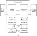
- FIG. 4 shows a three-phase converter 200 in an embodiment of the present invention.
- the three-phase converter 200 is connected between a direct current system 100 and an alternating current system 300.
- the three-phase converter 200 includes a switching network 201, a three-phase filter 202 connected to the switching network 201, a sampling unit 203 connected to the three-phase filter 202, a control unit 204 connected to the three-phase sampling unit 203, an active damping unit 205 connected to both the control unit 204 and the sampling unit 203, and a modulation unit 206 connected between the active damping unit 205 and the switching network 201.
- the active damping unit 205 determines a regulation component of each phase circuit according to different statuses of phase currents of three-phase currents in the three-phase filter 202; superposes the regulation component of each phase circuit with the three-phase modulated waves generated by the control unit 204, to generate corrected three-phase modulated waves; and then uses the corrected three-phase modulated waves to control the switching transistor of the switching network 201, thereby reducing the common-mode current of the three-phase converter 200.
- the foregoing direct current system 100 may be any power source that provides a direct current, and includes a battery, a solar photovoltaic panel, or the like.
- the foregoing alternating current system 300 may be any device or apparatus that requires alternating current input, and includes a power grid, a motor, or the like.
- An input end of the foregoing switching network 201 is connected to an output end of the direct current system 100.
- the switching network 201 is configured to convert the direct current of the direct current system 100 into a three-level alternating current output.
- the three-phase filter 202 is configured to convert the multi-level alternating current output of the switching network 201 into an alternating current having a sinusoidal or cosine waveform, so as to be transmitted to the alternating current system 300.
- the foregoing sampling unit 203 is configured to: obtain voltage and current signals in a hardware system, convert the voltage and current signals into a digital signal that is convenient for processing by the control unit 204, and output the digital signal to the control unit 204.
- the sampling unit 203 is specifically configured to: obtain three-phase currents and voltages in the three-phase filter 202 and separately perform sampling and measurement, to obtain three-phase currents i a , i b , and i c and three-phase voltages v ga , v gb , and v gc ; and provide the three-phase currents and voltages to the control unit 204 and the active damping unit 205.
- the foregoing control unit 204 is configured to: perform comparative calculation on sampled and converted voltage and current signals and a set reference value, perform corresponding signal processing, and output modulated waves.
- the control unit 204 is specifically configured to perform discontinuous pulse-width modulation (DPWM) according to the input three-phase currents i a , i b , and i c and three-phase voltages v ga , v gb , and v gc , to obtain modulated waves v a , v b , and v c .
- DPWM discontinuous pulse-width modulation
- the control unit 204 transfers the modulated waves v a , v b , and v c to the active damping unit 205.
- the foregoing active damping unit 205 is configured to: perform independent regulation on the three-phase currents i a , i b , and i c respectively by using mutually independent regulation functions to obtain regulation components v' a , v ' b , and v ' c that are in a one-to-one correspondence with the three-phase currents i a , i b , and i c , obtain a zero-sequence regulation component v 0 according to the regulation components v ' a , v ' b , and v ' c , separately add the zero-sequence regulation component v 0 to the three-phase modulated waves v a , v b , and v c that are output by the control unit 204 to obtain new three-phase modulated waves v a_mod , v b_mod , and v c_mod , and transmit the new three-phase modulated waves v a
- the foregoing active damping unit 205 includes a current regulator G a , a current regulator G b , a current regulator G c , and a zero-sequence regulation component calculator 2050.
- the current regulator G a , the current regulator G b , and the current regulator G c respectively receive, in a one-to-one correspondence, the three-phase currents i a , i b , and i c that are transferred by the sampling unit 203, respectively regulate the three-phase currents i a , i b , and i c by using the mutually independent regulation functions, and respectively output the regulation components v' a , v ' b , and v ' c to the zero-sequence regulation component calculator 2050.
- PI proportional integral
- PR proportional resonant
- the current regulator may be a regulator of another form, and correspondingly use a different regulation function.
- two or more types of regulators may be used in combination. The following lists some current regulators included in the present invention, but the present invention is not limited thereto.
- parameters represented by a same symbol have a same meaning. For the purpose of brevity, a parameter is described only at the first appearance.
- the current regulator may be a derivative regulator, and a regulation function G of the derivative regulator is:
- the three-phase current regulators in the active damping unit 205 may be set to different values, to respectively perform independent modulation on the three-phase currents and perform system correction in a control loop, so that an output can match a control loop of an existing symmetric system.
- An effect of the three-phase current regulators is an effect of added active damping.
- the regulation functions of the current regulators may be used as the regulation functions of the added virtual damping loop, where inputs are the currents, and outputs are the voltages, that is, the regulation components.
- the zero-sequence regulation component calculator 2050 receives the regulation components v' a , v ' b , and v ' c that are respectively output by the current regulator G a , the current regulator G b , and the current regulator G c , and calculates an average or a weighted average of the regulation components v' a , v ' b , and v ' c , where a result of the average or the weighted average is equal to the zero-sequence regulation component v 0 .
- the weighted average needs to be obtained by performing weighted averaging by using some weighting coefficients.
- the active damping unit 205 separately adds the zero-sequence regulation component v 0 to the three-phase modulated waves v a , v b , and v c that are output by the control unit 204 to obtain the new three-phase modulated waves v a_mod , v b_mod , and v c_mod , and transmits the new three-phase modulated waves v a_mod , v b_mod , and v c_mod to the modulation unit 206.
- the foregoing modulation unit 206 is configured to: compare the three-phase modulated waves with a carrier signal according to the modulated waves that are output by the control unit 204 and switch configuration in the hardware system, and output drive signals corresponding to switching devices.
- the modulation unit 206 is specifically configured to modulate the new three-phase modulated waves v a_mod , v b_mod , and v c_mod into drive signals of the switching network 201, to drive the switching network 201 to work.
- the foregoing three-phase converter 200 controls the switching network 201 by using the new three-phase modulated waves v a_mod , v b_mod , and v c_mod that are obtained through regulation by using the zero-sequence regulation component v 0 , to effectively suppress common-mode current resonance on the basis of original control by using the three-phase modulated waves v a , v b , and v c that are output by the control unit 204.
- the zero-sequence regulation component v 0 may be used to perform dynamic regulation in real time according to an entire three-phase system and a variation of the three-phase currents i a , i b , and i c , to cancel excited oscillation of common-mode current resonance caused by a drastic variation of the three-phase currents i a , i b , and i c , thereby ensuring stable and efficient operation of the three-phase system.
- a solid line depicts a Bode plot of a common-mode voltage to common-mode current regulation function of an active damping system in an embodiment of the present invention
- a dotted line depicts a Bode plot of a common-mode voltage to common-mode current regulation function of a damping-free system.
- a Bode plot is a method for illustrating a frequency response of a system.
- a Bode plot includes a magnitude plot (upper) and a phase plot (lower). Horizontal coordinates in both plots are drawn according to logarithmic scales of frequencies.
- a unit of a vertical coordinate in the magnitude plot is decibel (dB).
- the vertical coordinate represents an amplification factor of a common-mode current amplitude relative to a common-mode voltage amplitude, a larger value indicates a greater amplification factor.
- the three-phase converter in this embodiment of the present invention is applicable to various three-phase systems and is applicable to any system that needs three-phase input to drive switching devices.
- the three-phase converter is applicable to rectifier and inverter systems with two levels, three levels, five levels, or cascaded levels.
- switching network 201 In the various three-phase systems, other unit combinations, except the switching network 201, are the same and applicable. As shown in FIG. 7 , the following describes in detail a circuit structure of the switching network 201 by using an example in which a three-phase three-level inverter is applied to a photovoltaic inverter system.
- the switching network 201 includes a first voltage-dividing capacitor C1, a second voltage-dividing capacitor C2, a first switch combination Sa, a second switch combination Sb, and a third switch combination Sc.
- the first voltage-dividing capacitor C1 and the second voltage-dividing capacitor C2 are mutually connected in series between a positive electrode and a negative electrode of a direct current power source 100, and are configured to divide a voltage of the direct current power source 100.
- the first switch combination Sa, the second switch combination Sb, and the third switch combination Sc are mutually connected in parallel between the positive electrode and the negative electrode of the direct current power source 100.
- a series combination including the first voltage-dividing capacitor C1 and the second voltage-dividing capacitor C2 is connected in parallel to the first switch combination Sa, the second switch combination Sb, and the third switch combination Sc.
- the first switch combination Sa includes a first connection terminal Sa1 and a second connection terminal Sa2 that are respectively connected to the positive electrode and the negative electrode of the direct current power source, a third connection terminal Sa3 connected to a middle point of the series combination including the first voltage-dividing capacitor C1 and the second voltage-dividing capacitor C2, and a fourth connection terminal Sa4 connected to an input end of the three-phase filter.
- the second switch combination Sb includes a first connection terminal Sb1 and a second connection terminal Sb2 that are respectively connected to the positive electrode and the negative electrode of the direct current power source, a third connection terminal Sb3 connected to the middle point of the series combination including the first voltage-dividing capacitor C1 and the second voltage-dividing capacitor C2, and a fourth connection terminal Sb4 separately connected to three input ends of the three-phase filter.
- the third switch combination Sc includes a first connection terminal Sc1 and a second connection terminal Sc2 that are respectively connected to the positive electrode and the negative electrode of the direct current power source, a third connection terminal Sc3 connected to the middle point of the series combination including the first voltage-dividing capacitor C1 and the second voltage-dividing capacitor C2, and a fourth connection terminal Sc4 separately connected to the three input ends of the three-phase filter.
- the third connection terminals Sa3, Sb3, and Sc3 of the three switch combinations are respectively connected to the three input ends of the three-phase filter 202.
- Each of the fourth connection terminals Sa4, Sb4, and Sc4 is selectively connected to or disconnected from any one of the first, second, or third connection terminal of the switch combination to which the fourth connection terminal belongs, to implement conversion between the direct current and the alternating current.
- the fourth connection terminals Sa4, Sb4, and Sc4 selectively implement, by using disconnect and connect combinations of switching transistors in the switch combinations, the connection to or the disconnection from any one of the first, second, or third connection terminal of their respective switch combinations, to implement the conversion between the direct current and the alternating current.
- the three-phase filter 202 includes six inductors in three groups each including two inductors connected in series between the three fourth connection terminals Sa4, Sb4, and Sc4 of the switching network 201 and three input ends of the alternating current system 300; and includes three filtering capacitors C0 separately connected to the middle point of the series combination including the first voltage-dividing capacitor C1 and the second voltage-dividing capacitor C2 and respectively connected to middle points of the three groups of inductors each including two connected in series.
- the six inductors include a first converter-side inductor L1a, a second converter-side inductor L1b, a third converter-side inductor L1c, a first alternating current-side inductor L2a, a second alternating current-side inductor L2b, and a third alternating current-side inductor L2c.
- the first converter-side inductor L1a and the first alternating current-side inductor L2a are connected in series between the fourth connection terminal Sa4 of the first switch combination Sa and an input end of the alternating current system 300.
- the second converter-side inductor L1b and the second alternating current-side inductor L2b are connected in series between the fourth connection terminal Sb4 of the second switch combination Sb and an input end of the alternating current system 300.
- the third converter-side inductor L1c and the third alternating current-side inductor L2c are connected in series between the fourth connection terminal Sc4 of the third switch combination Sc and an input end of the alternating current system 300.
- One end of each of the filtering capacitors C0 is connected to the middle point of the series combination including the first voltage-dividing capacitor C1 and the second voltage-dividing capacitor C2, and the other end of each of the filtering capacitors C0 is connected to the middle point of one of the three groups of inductors.
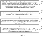
- another embodiment of the present invention includes a three-phase converter control method.
- the method is implemented in one of the hardware environments in the foregoing embodiment.
- the method includes the following steps:
- an active damping unit of the three-phase converter receives the three-phase currents i a , i b , and i c that are obtained through sampling and detection and transferred by the sampling unit.
- the three-phase currents i a , i b , and i c are respectively input to corresponding current regulators G a , G b , and G c .
- Independent regulation functions on the current regulators are used to respectively regulate the three-phase currents i a , i b , and i c , and the regulation components v' a , v ' b , and v' c are separately output to a zero-sequence regulation component calculator of the active damping unit.
- the current regulators and regulation functions used in this embodiment of the present invention are the same as those in the foregoing embodiment. Details are not described herein again.
- the zero-sequence regulation component calculator receives the regulation components v' a , v ' b , and v ' c that are respectively output by the current regulator G a , the current regulator G b , and the current regulator G c , and calculates an average or a weighted average of the regulation components v' a , v ' b , and v ' c , where a result of the average or the weighted average is equal to the zero-sequence regulation component v 0 .
- the weighted average needs to be obtained by performing weighted averaging by using some weighting coefficients.
- an error exists in a process of measuring and processing a variable such as a current, affecting precision of a final value obtained through calculation.
- Overall calculation precision is related to all the following: precision of a measurement device, an ambient temperature, and processing precision of a digital processor. Errors are unavoidable and ubiquitous, such as a quantization error caused by discrete rounding when an analog signal is converted into a digital signal, or a temperature error caused because a resistivity of a semiconductor material in a Hall sensor varies according to temperatures.
- the active damping unit separately adds the zero-sequence regulation component v 0 to the three-phase modulated waves v a , v b , and v c that are output by a control unit of the three-phase converter, to obtain the new three-phase modulated waves v a_mod , v b_mod , and v c_mod , and transmit the new three-phase modulated waves v a_mod , v b_mod , and v c_mod to a modulation unit of the three-phase converter.
- the modulation unit is configured to: compare the three-phase modulated waves and the carrier signal according to the modulated waves that are output by the control unit and switch configuration in a hardware system, and output drive signals corresponding to the switching devices.
- the modulation unit is specifically configured to modulate the new three-phase modulated waves v a_mod , v b_mod , and v c_mod into drive signals of a switching network of the three-phase converter, to drive the switching network to work.
- a three-phase converter is applied to a photovoltaic system.
- the photovoltaic system includes a photovoltaic cell panel and the three-phase converter connected between the photovoltaic cell panel and an alternating current power grid.
- the three-phase converter is configured to: convert, into multiple levels by using switching devices, a direct current that is output by the photovoltaic cell panel; output three-phase currents i a , i b , and i c after performing filtering processing based on the multiple levels; and perform independent regulation on the three-phase currents i a , i b , and i c respectively by using mutually independent regulation functions, to obtain regulation components v' a , v ' b , and v' c .
- the three-phase converter obtains a zero-sequence regulation component v 0 through calculation according to the regulation components v' a , v ' b , and v' c ; separately adds the zero-sequence regulation component v 0 to three-phase modulated waves v a , v b , and v c , to obtain new three-phase modulated waves v a_mod , v b_mod , and v c_mod ; and finally compares the new three-phase modulated waves v a_mod , v b_mod , and v c_mod with a carrier signal of the three-phase converter, and outputs drive signals of switching devices of the three-phase converter, so as to convert, into an alternating current, the direct current that is output by the photovoltaic cell panel and input the alternating current to the alternating current power grid.
- the three-phase converter includes a current regulator G a , a current regulator Gb, and a current regulator G c .
- the current regulator G a , the current regulator G b , and the current regulator G c respectively receive the three-phase currents i a , i b , and i c in a one-to-one correspondence, and respectively regulate the three-phase currents i a , i b , and i c by using the mutually independent regulation functions, to obtain the regulation components v ' a , v ' b , and v ' c that are in a one-to-one correspondence with the three-phase currents i a , i b , and i c .
- the three-phase converter further includes a zero-sequence regulation component calculator.
- the zero-sequence regulation component calculator receives the regulation components v ' a , v ' b , and v ' c that are respectively output by the current regulator G a , the current regulator G b , and the current regulator G c , and calculates an average or a weighted average of the regulation components v' a , v ' b , and v ' c , where a result of the average or the weighted average is equal to the zero-sequence regulation component v 0 .
- compositional structures and circuit design of the foregoing three-phase converter are all the same as related content described in the foregoing embodiment of present invention. Details are not described herein.
- a three-phase converter is applied to an electric vehicle.
- a power system of the electric vehicle includes a direct current power source, a three-phase motor, and a three-phase converter connected between the direct current power source and the three-phase motor.
- the three-phase converter is configured to: convert, into multiple levels by using switching devices, a direct current that is output by the photovoltaic cell panel; and output three-phase currents i a , i b , and i c after performing filtering processing based on the multiple levels.
- the three-phase converter includes a current regulator G a , a current regulator G b , a current regulator G c , and a zero-sequence regulation component calculator.
- the current regulator G a , the current regulator G b , and the current regulator G c are configured to: respectively receive the three-phase currents i a , ib, and i c in a one-to-one correspondence, and perform independent regulation on the three-phase currents i a , i b , and i c respectively by using mutually independent regulation functions, to obtain regulation components v' a , v ' b , and v' c .
- the zero-sequence regulation component calculator receives the regulation components v' a , v ' b , and v ' c that are respectively output by the current regulator G a , the current regulator G b , and the current regulator G c , and calculates an average or a weighted average of the regulation components v' a , v ' b , and v ' c , where a result of the average or the weighted average is equal to a zero-sequence regulation component v 0 .
- the three-phase converter is further configured to: compare new three-phase modulated waves v a_mod , v b_mod , and v c_mod with a carrier signal of the three-phase converter, and output drive signals of switching devices of the three-phase converter, so as to convert, into an alternating current, the direct current that is output by the direct current power source and input the alternating current to the three-phase motor.
- compositional structures and circuit design of the foregoing three-phase converter are all the same as related content described in the foregoing embodiment of present invention. Details are not described herein.
Description
- The present invention relates to the energy and power supply field, and in particular, to a three-phase converter and a three-phase converter control method.
- Along with development of the economy and society, the energy crisis becomes increasingly prominent and the global environment gradually deteriorates. Therefore, developing and using clean alternative energy has become an important goal in the energy industry. In the wake of the continuous development of new energy power generation, energy storage, and new energy automobile industries, as a core energy control apparatus, a converter becomes one of key factors in application of clean energy. The converter is an essential unit for implementing transfer of renewable energy, such as solar photovoltaic energy, to a power grid.
- Among various types of converters, three-phase converters are one type of most widely applied converters, and are used to connect a three-phase alternating current electrical power system and a direct current electrical power system and implement energy transfer between the two systems. Energy transfer is further distinguished into two working statuses, rectification and inversion, according to different energy flow directions. Energy transfer from the direct current system to the alternating current system is referred to as inversion, and energy transfer from the alternating current system to the direct current system is referred to as rectification.
- Therefore, in most application scenarios, rectification and inversion can be implemented by using a same system. A typical system structure of the system is shown in
FIG. 1 . A three-phase converter is connected between a direct current system and an alternating current system, and includes a switching network, a filter, and a controller that controls the switching network. - Conversion efficiency and electric energy quality are two key technical indicators of a three-phase converter. However, a modulation method directly affects a connectivity status of switching devices, and therefore, is one of key factors that affect the conversion efficiency and electric energy quality of the three-phase converter.
- A commonly used modulation method is pulse-width modulation (PWM), that is, a width of a driving pulse of each device on a switching network is controlled. A most direct implementation is to compare a carrier and a modulated wave, and control a connectivity status of a switching device by using a result of the comparison.
- PWM may be further categorized into continuous pulse-width modulation (CPWM) and discontinuous pulse-width modulation (DPWM). The CPWM means that there is always a switching action in each phase bridge arm in each switching period. Common methods include sinusoidal pulse-width modulation (SPWM), space vector pulse-width modulation (SVPWM), and third-harmonic-injection pulse-width modulation (THIPWM). The DPWM means that a phase bridge arm of a converter is clamped on a positive direct current bus or a negative direct current bus in a specific switching period, and a switching device of this phase is always connected or always disconnected in a clamping interval and there is no switching action. Common DPWM modulation methods include DPWM0, DPWM1, DPWM2, DPWM3, DPWMMAX, DPWMMIN, GDPWM, and so on.
- Compared with the CPWM, the DPWM has a smaller quantity of switching times. Therefore, a switching loss is relatively small, and a consequential benefit is that efficiency of a converter can be improved.
- In specific implementation, a DPWM modulated wave may be implemented by superposing an equivalent common-mode component on a CPWM modulated wave. For example, a DPWM modulated waveform and an SPWM modulated waveform in an industrial frequency period (50 Hz) are compared, as shown in
FIG. 2 . A difference between the two modulated waves is a common-mode signal waveform shown inFIG. 2 . - The DPWM modulated wave may be equivalent to a sum of SPWM wave and a common-mode signal. Therefore, an output characteristic of DPWM wave is affected by both an output characteristic of SPWM and an output characteristic of the common-mode signal, and an extra common-mode voltage source is formed at a bridge arm port of a converter. The common-mode voltage source and a common-mode loop in a system interact with each other, affecting system performance.
- As shown in
FIG. 3 , in a typical three-level LCL filter converter, to reduce a common-mode current transferred to an alternating current system by the converter, a middle point of capacitors of the LCL filter is connected to a middle point of capacitors on a direct current bus, to form a new common-mode loop. This is equivalent to splitting a common-mode current generated by the converter, so that most of the common-mode current is directed back to a direct current side of the converter by using a connection loop of the LCL filter. However, a series connection of an inductor and a capacitor exists in the connection loop, and there is a natural series resonant frequency. If the frequency overlaps a frequency range of a common-mode voltage source generated because of DPWM modulation, series resonance is generated, causing sharp fluctuation of the common-mode current, thereby affecting system stability. - EYYUP DEMIRKUTLU ET AL: "Output Voltage Control of A Four-Leg Inverter Based Three-Phase UPS by Means of Stationary Frame Resonant Filter Banks", ELECTRIC MACHINES & DRIVES CONFERENCE, 2007. IEMDC '07. IEEE INTERNATIONAL, IEEE, PISCATAWAY, NJ, USA, 1 May 2007, pages 880-885 discloses a method for high performance output voltage control of a four-leg inverter (FLI) based three-phase UPS.
- TENG LIU ET AL: "Virtual impedance-based active damping for LOL resonance in grid-connected voltage source inverters with grid current feedback", 2016 IEEE ENERGY CONVERSION CONGRESS AND EXPOSITION (ECCE), 1 September 2016, pages 1-8, discloses a straightforward design method to determine the parameters of the active damping controller.
- PICAS R ET AL: "Improving capacitor voltage ripples and power losses of modular multilevel converters through discontinuous modulation", IECON 2013 - 39TH ANNUAL CONFERENCE OF THE IEEE INDUSTRIAL ELECTRONICS SOCIETY, IEEE, 10 November 2013, pages 6233-6238 discloses a discontinuous modulation technique for reducing the amplitude of the capacitor voltage ripples and the switching losses, especially at low modulation indices.
-
US 2012/249043 A1 discloses a method for pulse width modulation control of a multiple phase drive that includes identifying a set of at least one phase from the plurality of phases for the drive as eligible for clamping to one of a plurality of extreme power supply voltages, including excluding from the set of eligible phases those phases with intermediate control signal levels and excluding phases according to a proximity criterion on the control signal levels. A phase is selected from the set of eligible phases. A first offset signal is determined as a difference between a control signal level for the selected phase and an extreme control signal level associated with one of the plurality of extreme power supply voltages. A modified control signal is determined for each of the phases for the drive, by forming a combination of the first offset signal and a control signal level for each phase to determine the modified control signal for each phase. - QIANG SONG ET AL: "A neutral-point potential balancing algorithm for three-level NPC inverters using analytically injected zero- sequence voltage", APEC 2003. 18TH. ANNUAL IEEE APPLIED POWER ELECTRONICS CONFERENCE AND EXPOSITION. MIAMI BEACH, FL, FEB. 9 - 13, 2003; [ANNUAL APPLIED POWER ELECTRONICS CONFERENCE], NEW YORK, NY: IEEE, US, 9 February 2003 (2003-02-09), pages 228-233 vol.1, discloses that, based on the zero-sequence component of the reference voltages, the neutral-point variation and balancing control for three-level neutral-point-clamped inverter are analyzed. An analytical method is proposed to accurately calculate the injected zero-sequence voltage for NP balancing. Based on the analytical analysis, the limitation of NP balancing control is revealed and the NP-fully-controllable region is presented. A real-time NP balancing algorithm is proposed as well. The feasibility of the proposed method is verified using simulation results for a 6kV/1800kVA medium voltage drive.
- Embodiments of the present invention provide a three-phase converter and a three-phase converter control method, which are used to reduce a common-mode current in the three-phase converter, thereby effectively improving stability and efficiency of the converter. The invention is defined by the independent claims. All the technical features of the independent claims are mandatory and not optional, irrespective of any statements to the contrary in the following passages. Preferred embodiments are described by the dependent claims.
- According to a first aspect, a three-phase converter is provided, and is configured to be connected between a direct current system and an alternating current system to perform interconversion between a direct current and an alternating current, where the three-phase converter includes a switching network, a three-phase filter connected to the switching network, a sampling unit connected to the three-phase filter, a control unit connected to the three-phase sampling unit, an active damping unit connected to both the control unit and the sampling unit, and a modulation unit connected between the active damping unit and the switching network, where the sampling unit is configured to: obtain three-phase currents i a, i b, and i c that are output by the three-phase filter, and send the three-phase currents i a, i b, and i c to the active damping unit; the active damping unit is configured to: obtain, according to the three-phase currents i a, i b, and i c, regulation components v' a, v'b, and v'c that are in a one-to-one correspondence with the three-phase currents i a, i b, and i c, obtain a zero-sequence regulation component v 0 according to the regulation components v' a, v'b, and v'c, separately add the zero-sequence regulation component v 0 to three-phase modulated waves va, vb, and vc that are output by the control unit to obtain new three-phase modulated waves v a_mod, v b_mod, and v c_mod, and transmit the new three-phase modulated waves v a_mod, v b_mod, and v c_mod to the modulation unit; and the modulation unit is configured to modulate the new three-phase modulated waves v a_mod, v b_mod, and v c_mod into drive signals of the switching network, to drive the switching network to output the multiple levels to the three-phase filter; and the three-phase filter is configured to convert the multiple levels into an alternating current that is input to the alternating current system; wherein the active damping unit comprises a current regulator Ga, a current regulator Gb, and a current regulator Gc; and the current regulator Ga, the current regulator Gb, and the current regulator Gc respectively receive the three-phase currents i a, i b, and i c in a one-to-one correspondence, and regulate the three-phase currents i a, i b, and i c respectively by using mutually independent regulation functions, to obtain the regulation components v' a, v'b, and v'c that are in a one-to-one correspondence with the three-phase currents i a, i b, and i c; and wherein the active damping unit further comprises a zero-sequence regulation component calculator; and the zero-sequence regulation component calculator receives the regulation components v' a, v'b, and v'c that are respectively output by the current regulator Ga, the current regulator Gb, and the current regulator Gc, and calculates an average or a weighted average of the regulation components v' a, v'b, and v'c, wherein a result of the average or the weighted average is the zero-sequence regulation component v0 .
- A second aspect provides a three-phase converter control method, used to control a three-phase converter connected between a direct current system and an alternating current system to perform interconversion between a direct current and an alternating current, where the method includes: step 101: obtaining three-phase currents i a, i b, and i c in the three-phase converter, and respectively inputting the three-phase currents i a, i b, and i c one by one to corresponding current regulators Ga, Gb, and Gc, to obtain regulation components v' a, v'b, and v'c; step 102: obtaining a zero-sequence regulation component v 0 through calculation according to the regulation components v' a, v'b, and v'c; step 103: separately adding the zero-sequence regulation component v 0 to three-phase modulated waves va, vb, and vc, to obtain new three-phase modulated waves v a_mod, v b_mod, and v c_mod; and step 104: comparing the new three-phase modulated waves v a_mod, v b_mod, and v c_mod with a carrier signal of the three-phase converter, and outputting drive signals of switching devices of the three-phase converter, wherein the obtaining a zero-sequence regulation component v0 through calculation according to the regulation components v' a, v'b, and v'c comprises: calculating an average or a weighted average of the regulation components v' a, v'b, and v'c, wherein a result of the average or the weighted average is the zero-sequence regulation component v0 .
-
-
FIG. 1 is a schematic structural diagram of a three-phase converter in the prior art; -
FIG. 2 is a diagram showing waveform comparison between a DPWM modulated wave and a CPWM modulated wave in the prior art; -
FIG. 3 is a schematic structural diagram of an LCL filter converter in the prior art; -
FIG. 4 is a schematic diagram of a three-phase converter according to an embodiment of the present invention; -
FIG. 5 is a schematic structural diagram of an active damping unit according to an embodiment of the present invention; -
FIG. 6 is a Bode plot of transfer functions from a common-mode voltage to a common-mode current of an active damping system in an embodiment of the present invention and a damping-free system in the prior art; -
FIG. 7 is a circuit diagram of a three-phase converter according to an embodiment of the present invention; -
FIG. 8 is a flowchart of a three-phase converter control method according to another embodiment of the present invention; and -
FIG. 9 is a schematic diagram of a power system of an electric vehicle according to still another embodiment of the present invention. - In the following description the term "embodiment" may have been used for subject-matter that is not part of the invention as defined by the appended claims. Only those examples that comprise all the features of the independent claims are part of the invention and thus embodiments of the invention. Parts of the subject-matter of the description not covered by the claims constitutes background art or examples useful for understanding the invention. The technical solutions of the present invention are further described in detail with reference to accompanying drawings and embodiments as follows:
- A three-phase converter in an embodiment of the present invention is configured to convert a direct current into an alternating current, or convert an alternating current into a direct current. For example, in a photovoltaic power supply system, a direct current generated by a photovoltaic solar panel is converted, by using a converter, into an alternating current having a same frequency as a power grid, and regulation components v' a, v'b, and v'c; step 103: separately adding the zero-sequence regulation component v 0 to three-phase modulated waves va, vb, and vc, to obtain new three-phase modulated waves v a_mod, v b_mod, and v c_mod; and step 104: comparing the new three-phase modulated waves va_mod, v b_mod, and v c_mod with a carrier signal of the three-phase converter, and outputting drive signals of switching devices of the three-phase converter.
- With reference to the second aspect, in a first implementation of the second aspect, the obtaining a zero-sequence regulation component v 0 through calculation according to the regulation components v'a, v'b, and v'c includes:
calculating an average or a weighted average of the regulation components v'a, v'b, and v'c, where a result of the average or the weighted average is equal to the zero-sequence regulation component v 0. - With reference to the second aspect or the first implementation of the second aspect, in a second implementation of the second aspect, the obtaining a zero-sequence regulation component v 0 through calculation according to the regulation components v' a, v'b, and v'c includes:
calculating a weighted average of the regulation components v' a, v'b, and v'c, to obtain the zero-sequence regulation component v 0, where a calculation formula is:
zero-sequenceregulation component 
- A third aspect provides a photovoltaic system, including a photovoltaic cell panel and a three-phase converter that is connected between the photovoltaic cell panel and an alternating current power grid, where the three-phase converter is configured to obtain regulation components v' a, v'b, and v'c according to three-phase currents i a, i b, and i c in the three-phase converter; and the three-phase converter obtains a zero-sequence regulation component v 0 through calculation according to the regulation components v' a, v'b, and v'c, separately adds the zero-sequence regulation component v 0 to three-phase modulated waves va, vb, and vc to obtain new three-phase modulated waves v a_mod, v b_mod, and v c_mod, and finally compares the new three-phase modulated waves v a_mod, v b_mod, and v c_mod with a carrier signal of the three-phase converter and outputs drive signals of switching devices of the three-phase converter, so as to convert, into an alternating current, a direct current that is output by the photovoltaic cell panel and input the alternating current to the alternating current power grid.
- A fourth aspect provides a power system of an electric vehicle, including a direct current power source, a motor, and a three-phase converter connected between the direct current power source and the motor, where the three-phase converter includes a current regulator Ga, a current regulator Gb, a current regulator Gc, and a zero-sequence regulation component calculator; the three-phase converter is configured to respectively input three-phase currents i a, i b, and i c in the three-phase converter to the current regulator Ga, the current regulator Gb, and the current regulator Gc in a one-to-one correspondence, to respectively obtain corresponding regulation components v' a, v'b, and v'c; the zero-sequence regulation component calculator receives the regulation components v' a, v'b, and v'c that are respectively output by the current regulator Ga, the current regulator Gb, and the current regulator Gc, and calculates an average or a weighted average of the regulation components v'a, v'b, and v'c, where a result of the average or the weighted average is equal to a zero-sequence regulation component v 0; the current regulator Ga, the current regulator Gb, and the current regulator Gc respectively receive the three-phase currents i a, i b, and i c in a one-to-one correspondence, and regulate the three-phase currents i a, i b, and i c respectively by using mutually independent regulation functions, to obtain the regulation components v' a, v'b, and v'c that are in a one-to-one correspondence with the three-phase currents i a, i b, and i c; and the three-phase converter compares new three-phase modulated waves v a_mod, v b_mod, and v c_mod with a carrier signal of the three-phase converter and outputs drive signals of switching devices of the three-phase converter, so as to convert, into an alternating current, a direct current that is output by the direct current power source and input the alternating current to the motor.
- If a relatively large common-mode current is generated when the foregoing three-phase converter directly uses the three-phase modulated waves generated by the control unit to control a switching transistor of the switching network, the active damping unit determines a regulation component of each phase circuit according to different statuses of the phase currents of the three-phase currents in the three-phase filter; superposes the regulation component of each phase circuit with the three-phase modulated waves generated by the control unit, to generate corrected three-phase modulated waves; and then uses the corrected three-phase modulated waves to control the switching transistor of the switching network, thereby reducing the common-mode current of the three-phase converter.
-
-
FIG. 1 is a schematic structural diagram of a three-phase converter in the prior art; -
FIG. 2 is a diagram showing waveform comparison between a DPWM modulated wave and a CPWM modulated wave in the prior art; -
FIG. 3 is a schematic structural diagram of an LCL filter converter in the prior art; -
FIG. 4 is a schematic diagram of a three-phase converter according to an embodiment of the present invention; -
FIG. 5 is a schematic structural diagram of an active damping unit according to an embodiment of the present invention; -
FIG. 6 is a Bode plot of transfer functions from a common-mode voltage to a common-mode current of an active damping system in an embodiment of the present invention and a damping-free system in the prior art; -
FIG. 7 is a circuit diagram of a three-phase converter according to an embodiment of the present invention; -
FIG. 8 is a flowchart of a three-phase converter control method according to another embodiment of the present invention; and -
FIG. 9 is a schematic diagram of a power system of an electric vehicle according to still another embodiment of the present invention. - The technical solutions of the present invention are further described in detail with reference to accompanying drawings and embodiments as follows:
A three-phase converter in an embodiment of the present invention is configured to convert a direct current into an alternating current, or convert an alternating current into a direct current. For example, in a photovoltaic power supply system, a direct current generated by a photovoltaic solar panel is converted, by using a converter, into an alternating current having a same frequency as a power grid, and the alternating current is transferred to the power grid, thereby implementing integration of the photovoltaic power supply system and the power grid. In an electric vehicle, a three-phase converter may implement bidirectional work. For example, a direct current that is output by a battery of the electric vehicle is converted into an alternating current by the three-phase converter, and the alternating current is output to a motor. When the electric vehicle decelerates, a reverse alternating current generated by the motor may be converted, by the three-phase converter, into a direct current to charge the battery. -
FIG. 4 shows a three-phase converter 200 in an embodiment of the present invention. The three-phase converter 200 is connected between a directcurrent system 100 and an alternating current system 300. The three-phase converter 200 includes a switching network 201, a three-phase filter 202 connected to the switching network 201, a sampling unit 203 connected to the three-phase filter 202, a control unit 204 connected to the three-phase sampling unit 203, an active damping unit 205 connected to both the control unit 204 and the sampling unit 203, and a modulation unit 206 connected between the active damping unit 205 and the switching network 201. - If a relatively large common-mode current is generated when three-phase modulated waves generated by the control unit 204 are directly used to control a switching transistor of the switching network 201, the active damping unit 205 determines a regulation component of each phase circuit according to different statuses of phase currents of three-phase currents in the three-phase filter 202; superposes the regulation component of each phase circuit with the three-phase modulated waves generated by the control unit 204, to generate corrected three-phase modulated waves; and then uses the corrected three-phase modulated waves to control the switching transistor of the switching network 201, thereby reducing the common-mode current of the three-phase converter 200.
- The foregoing direct
current system 100 may be any power source that provides a direct current, and includes a battery, a solar photovoltaic panel, or the like. - The foregoing alternating current system 300 may be any device or apparatus that requires alternating current input, and includes a power grid, a motor, or the like.
- An input end of the foregoing switching network 201 is connected to an output end of the direct
current system 100. The switching network 201 is configured to convert the direct current of the directcurrent system 100 into a three-level alternating current output. The three-phase filter 202 is configured to convert the multi-level alternating current output of the switching network 201 into an alternating current having a sinusoidal or cosine waveform, so as to be transmitted to the alternating current system 300. - The foregoing sampling unit 203 is configured to: obtain voltage and current signals in a hardware system, convert the voltage and current signals into a digital signal that is convenient for processing by the control unit 204, and output the digital signal to the control unit 204. The sampling unit 203 is specifically configured to: obtain three-phase currents and voltages in the three-phase filter 202 and separately perform sampling and measurement, to obtain three-phase currents i a, i b, and i c and three-phase voltages v ga, v gb, and v gc; and provide the three-phase currents and voltages to the control unit 204 and the active damping unit 205.
- The foregoing control unit 204 is configured to: perform comparative calculation on sampled and converted voltage and current signals and a set reference value, perform corresponding signal processing, and output modulated waves. The control unit 204 is specifically configured to perform discontinuous pulse-width modulation (DPWM) according to the input three-phase currents i a, i b , and i c and three-phase voltages v ga, v gb, and v gc, to obtain modulated waves v a, v b, and v c. The control unit 204 transfers the modulated waves v a, v b, and v c to the active damping unit 205.
- The foregoing active damping unit 205 is configured to: perform independent regulation on the three-phase currents i a, i b, and i c respectively by using mutually independent regulation functions to obtain regulation components v' a, v'b, and v' c that are in a one-to-one correspondence with the three-phase currents i a , i b, and i c , obtain a zero-sequence regulation component v 0 according to the regulation components v'a, v'b, and v'c, separately add the zero-sequence regulation component v 0 to the three-phase modulated waves va, vb, and vc that are output by the control unit 204 to obtain new three-phase modulated waves v a_mod, v b_mod, and v c_mod, and transmit the new three-phase modulated waves v a_mod, v b_mod, and v c_mod to the modulation unit 206.
- As shown in
FIG. 5 , the foregoing active damping unit 205 includes a current regulator Ga, a current regulator Gb, a current regulator Gc, and a zero-sequence regulation component calculator 2050. The current regulator Ga, the current regulator Gb, and the current regulator Gc respectively receive, in a one-to-one correspondence, the three-phase currents i a, i b, and i c that are transferred by the sampling unit 203, respectively regulate the three-phase currents i a, i b, and i c by using the mutually independent regulation functions, and respectively output the regulation components v' a, v'b, and v'c to the zero-sequence regulation component calculator 2050. - For example, at least one of the regulators may be a proportional integral (PI) regulator, and a regulation function G of the PI regulator is:

G=v'a/ia =v'b /i b= v'c /ic, k p is a proportion coefficient, k i is an integral coefficient, and s is a complex frequency, that is, a complex number is used to represent a frequency and a phase of an input signal. - The current regulator may be a proportional resonant (PR) regulator, and a regulation function G of the PR regulator is:

G is a ratio of an output voltage to an input current, for example, G=v'a/ia =v'b /i b= v'c /ic, in addition, both k p and k r are proportional constants, k p is a proportion coefficient, k r is a resonance coefficient, ω 0 is a resonant frequency of a circuit of the converter, and s is a complex frequency. - Alternatively, the current regulator may be a regulator of another form, and correspondingly use a different regulation function. Further, two or more types of regulators may be used in combination. The following lists some current regulators included in the present invention, but the present invention is not limited thereto. In addition, in these regulators, parameters represented by a same symbol have a same meaning. For the purpose of brevity, a parameter is described only at the first appearance.
- The current regulator may be a derivative regulator, and a regulation function G of the derivative regulator is:
- G = Ks , where
- G=v'a/ia =v'b /i b= v'c /ic, K is a proportion coefficient, and s is a complex frequency.
- Alternatively, the current regulator may be a high-pass filter, and a regulation function G of the high-pass filter is:

G=v'a /i'a =v'b /i b=v'c /i c , K is a proportion coefficient, ω HF is a cut-off frequency, and s is a complex frequency. - Alternatively, the current regulator may be a lead-lag regulator, and a regulation function G of the lead-lag regulator is:

G=v'a /ia =v' b/i b=v' c/i c , K is a proportion coefficient, ω max is a maximum phase-shift frequency, k f is a regulation coefficient, and s is a complex frequency. - Alternatively, the current regulator may be a second-order generalized integral regulator, and a regulation function G of the second-order generalized integral regulator is:

G=v' a/ia =v' b/i b=v' c/i c , ω 1 is a resonant frequency, k is a damping coefficient, and s is a complex frequency. - Alternatively, the current regulator may be a pole-zero placement regulator, and a regulation function G of the pole-zero placement regulator is:

G=v' a/i a=v' b/i b=v' c/i c , K is a proportion coefficient, z 1, z 2, ..., and z m are zeros, p 1 , p 2 , ..., and p n are poles, and s is a complex frequency. - When a three-phase system in which the active damping unit 205 is located is an asymmetric system, the three-phase current regulators in the active damping unit 205 may be set to different values, to respectively perform independent modulation on the three-phase currents and perform system correction in a control loop, so that an output can match a control loop of an existing symmetric system. An effect of the three-phase current regulators is an effect of added active damping. The regulation functions of the current regulators may be used as the regulation functions of the added virtual damping loop, where inputs are the currents, and outputs are the voltages, that is, the regulation components.
- The zero-sequence regulation component calculator 2050 receives the regulation components v' a, v'b, and v'c that are respectively output by the current regulator Ga, the current regulator Gb, and the current regulator Gc, and calculates an average or a weighted average of the regulation components v' a, v'b, and v'c, where a result of the average or the weighted average is equal to the zero-sequence regulation component v 0. For example, the average is:

- In addition, the weighted average needs to be obtained by performing weighted averaging by using some weighting coefficients.
- The active damping unit 205 separately adds the zero-sequence regulation component v 0 to the three-phase modulated waves va, vb, and vc that are output by the control unit 204 to obtain the new three-phase modulated waves v a_mod, v b_mod, and v c_mod, and transmits the new three-phase modulated waves v a_mod, v b_mod, and v c_mod to the modulation unit 206.
- Addition relationships between the zero-sequence regulation component v 0 and the three-phase modulated waves va, vb, and vc that are output by the control unit 204 are as follows:


- The foregoing modulation unit 206 is configured to: compare the three-phase modulated waves with a carrier signal according to the modulated waves that are output by the control unit 204 and switch configuration in the hardware system, and output drive signals corresponding to switching devices. The modulation unit 206 is specifically configured to modulate the new three-phase modulated waves v a_mod, v b_mod, and v c_mod into drive signals of the switching network 201, to drive the switching network 201 to work.
- The foregoing three-phase converter 200 controls the switching network 201 by using the new three-phase modulated waves v a_mod, v b_mod, and v c_mod that are obtained through regulation by using the zero-sequence regulation component v 0, to effectively suppress common-mode current resonance on the basis of original control by using the three-phase modulated waves va, vb, and vc that are output by the control unit 204. In addition, the zero-sequence regulation component v 0 may be used to perform dynamic regulation in real time according to an entire three-phase system and a variation of the three-phase currents i a, i b, and i c , to cancel excited oscillation of common-mode current resonance caused by a drastic variation of the three-phase currents i a, i b, and i c , thereby ensuring stable and efficient operation of the three-phase system.
- As shown in
FIG. 6 , a solid line depicts a Bode plot of a common-mode voltage to common-mode current regulation function of an active damping system in an embodiment of the present invention, and a dotted line depicts a Bode plot of a common-mode voltage to common-mode current regulation function of a damping-free system. A Bode plot is a method for illustrating a frequency response of a system. A Bode plot includes a magnitude plot (upper) and a phase plot (lower). Horizontal coordinates in both plots are drawn according to logarithmic scales of frequencies. A unit of a vertical coordinate in the magnitude plot is decibel (dB). The vertical coordinate represents an amplification factor of a common-mode current amplitude relative to a common-mode voltage amplitude, a larger value indicates a greater amplification factor. It can be seen from the magnitude plots inFIG. 6 that an apparent resonant peak exists in a characteristic of the damping-free system, and a resonant peak in a characteristic of the active damping system is obviously suppressed. In addition, the active damping system maintains system characteristics similar to those of the damping-free system except the resonant peak. Therefore, it can be learned that, in this embodiment of the present invention, common-mode current resonance can be effectively suppressed, and characteristics of other aspects of the system do not deteriorate because an active damping technology is introduced. - The three-phase converter in this embodiment of the present invention is applicable to various three-phase systems and is applicable to any system that needs three-phase input to drive switching devices. For example, the three-phase converter is applicable to rectifier and inverter systems with two levels, three levels, five levels, or cascaded levels.
- In the various three-phase systems, other unit combinations, except the switching network 201, are the same and applicable. As shown in
FIG. 7 , the following describes in detail a circuit structure of the switching network 201 by using an example in which a three-phase three-level inverter is applied to a photovoltaic inverter system. - The switching network 201 includes a first voltage-dividing capacitor C1, a second voltage-dividing capacitor C2, a first switch combination Sa, a second switch combination Sb, and a third switch combination Sc.
- The first voltage-dividing capacitor C1 and the second voltage-dividing capacitor C2 are mutually connected in series between a positive electrode and a negative electrode of a direct
current power source 100, and are configured to divide a voltage of the directcurrent power source 100. - The first switch combination Sa, the second switch combination Sb, and the third switch combination Sc are mutually connected in parallel between the positive electrode and the negative electrode of the direct
current power source 100. In addition, a series combination including the first voltage-dividing capacitor C1 and the second voltage-dividing capacitor C2 is connected in parallel to the first switch combination Sa, the second switch combination Sb, and the third switch combination Sc. - The first switch combination Sa includes a first connection terminal Sa1 and a second connection terminal Sa2 that are respectively connected to the positive electrode and the negative electrode of the direct current power source, a third connection terminal Sa3 connected to a middle point of the series combination including the first voltage-dividing capacitor C1 and the second voltage-dividing capacitor C2, and a fourth connection terminal Sa4 connected to an input end of the three-phase filter.
- The second switch combination Sb includes a first connection terminal Sb1 and a second connection terminal Sb2 that are respectively connected to the positive electrode and the negative electrode of the direct current power source, a third connection terminal Sb3 connected to the middle point of the series combination including the first voltage-dividing capacitor C1 and the second voltage-dividing capacitor C2, and a fourth connection terminal Sb4 separately connected to three input ends of the three-phase filter.
- The third switch combination Sc includes a first connection terminal Sc1 and a second connection terminal Sc2 that are respectively connected to the positive electrode and the negative electrode of the direct current power source, a third connection terminal Sc3 connected to the middle point of the series combination including the first voltage-dividing capacitor C1 and the second voltage-dividing capacitor C2, and a fourth connection terminal Sc4 separately connected to the three input ends of the three-phase filter.
- The third connection terminals Sa3, Sb3, and Sc3 of the three switch combinations are respectively connected to the three input ends of the three-phase filter 202.
- Each of the fourth connection terminals Sa4, Sb4, and Sc4 is selectively connected to or disconnected from any one of the first, second, or third connection terminal of the switch combination to which the fourth connection terminal belongs, to implement conversion between the direct current and the alternating current.
- In the switch combinations, the fourth connection terminals Sa4, Sb4, and Sc4 selectively implement, by using disconnect and connect combinations of switching transistors in the switch combinations, the connection to or the disconnection from any one of the first, second, or third connection terminal of their respective switch combinations, to implement the conversion between the direct current and the alternating current.
- The three-phase filter 202 includes six inductors in three groups each including two inductors connected in series between the three fourth connection terminals Sa4, Sb4, and Sc4 of the switching network 201 and three input ends of the alternating current system 300; and includes three filtering capacitors C0 separately connected to the middle point of the series combination including the first voltage-dividing capacitor C1 and the second voltage-dividing capacitor C2 and respectively connected to middle points of the three groups of inductors each including two connected in series.
- The six inductors include a first converter-side inductor L1a, a second converter-side inductor L1b, a third converter-side inductor L1c, a first alternating current-side inductor L2a, a second alternating current-side inductor L2b, and a third alternating current-side inductor L2c. The first converter-side inductor L1a and the first alternating current-side inductor L2a are connected in series between the fourth connection terminal Sa4 of the first switch combination Sa and an input end of the alternating current system 300. The second converter-side inductor L1b and the second alternating current-side inductor L2b are connected in series between the fourth connection terminal Sb4 of the second switch combination Sb and an input end of the alternating current system 300. The third converter-side inductor L1c and the third alternating current-side inductor L2c are connected in series between the fourth connection terminal Sc4 of the third switch combination Sc and an input end of the alternating current system 300.
- One end of each of the filtering capacitors C0 is connected to the middle point of the series combination including the first voltage-dividing capacitor C1 and the second voltage-dividing capacitor C2, and the other end of each of the filtering capacitors C0 is connected to the middle point of one of the three groups of inductors.
- As shown in
FIG. 8 , another embodiment of the present invention includes a three-phase converter control method. The method is implemented in one of the hardware environments in the foregoing embodiment. The method includes the following steps: -
Step 101. Obtain three-phase currents i a, i b, and i c in a three-phase converter, and perform independent regulation on the three-phase currents i a, i b, and i c respectively by using mutually independent regulation functions, to obtain regulation components v' a, v'b, and v'c that are in a one-to-one correspondence with the three-phase currents i a, i b, and i c. -
Step 102. Obtain a zero-sequence regulation component v 0 through calculation according to the regulation components v' a, v'b, and v' c. -
Step 103. Separately add the zero-sequence regulation component v 0 to three-phase modulated waves va, vb, and vc, to obtain new three-phase modulated waves v a_mod, v b_mod, and v c_mod. -
Step 104. Compare the new three-phase modulated waves v a_mod, v b_mod, and v c_mod with a carrier signal of the three-phase converter, and output drive signals of switching devices of the three-phase converter. - In
step 101, an active damping unit of the three-phase converter receives the three-phase currents i a, i b, and i c that are obtained through sampling and detection and transferred by the sampling unit. The three-phase currents i a, i b, and i c are respectively input to corresponding current regulators Ga, Gb, and Gc. Independent regulation functions on the current regulators are used to respectively regulate the three-phase currents i a, i b, and i c , and the regulation components v' a, v'b, and v' c are separately output to a zero-sequence regulation component calculator of the active damping unit. The current regulators and regulation functions used in this embodiment of the present invention are the same as those in the foregoing embodiment. Details are not described herein again. - In
step 102, the zero-sequence regulation component calculator receives the regulation components v' a, v'b, and v'c that are respectively output by the current regulator Ga, the current regulator Gb, and the current regulator Gc, and calculates an average or a weighted average of the regulation components v' a, v'b, and v'c, where a result of the average or the weighted average is equal to the zero-sequence regulation component v 0. For example, the average is:
- In addition, the weighted average needs to be obtained by performing weighted averaging by using some weighting coefficients. For example, an error exists in a process of measuring and processing a variable such as a current, affecting precision of a final value obtained through calculation. Overall calculation precision is related to all the following: precision of a measurement device, an ambient temperature, and processing precision of a digital processor. Errors are unavoidable and ubiquitous, such as a quantization error caused by discrete rounding when an analog signal is converted into a digital signal, or a temperature error caused because a resistivity of a semiconductor material in a Hall sensor varies according to temperatures.
- Therefore, to implement a high-precision control technology, correction and compensation need to be performed for an overall system error in a control phase.
- In the three-phase converter, internal temperatures of the converter are uneven because of a thermal conductivity characteristic of a system. As a result, ambient temperatures at locations of three-phase current Hall sensors are different. Therefore, sampled values of the three-phase currents are respectively 99%, 99.5%, and 99.2% of actual values (the precision may be obtained by using an additional testing means).
- Therefore, when the zero-sequence component is calculated, sampling and calculation precision of each phase needs to be considered, and the regulation components v' a, v'b, and v'c are compensated.
- After the obtained regulation components v' a, v'b, and v'c are transferred to the zero-sequence regulation component calculator, the zero-sequence regulation component v 0 is output, and

k1, k2, and k3 are three-phase weighting coefficients, and are related to the sampling precision, where k1 is equal to 1.010 (that is, 100/99), k2 is equal to 1.005 (100/99.5), and k3 is equal to 1.008 (100/99.2). - In the foregoing
step 103, the active damping unit separately adds the zero-sequence regulation component v 0 to the three-phase modulated waves va, vb, and vc that are output by a control unit of the three-phase converter, to obtain the new three-phase modulated waves v a_mod, v b_mod, and v c_mod, and transmit the new three-phase modulated waves v a_mod, v b_mod, and v c_mod to a modulation unit of the three-phase converter. - Addition relationships between the zero-sequence regulation component v 0 and the three-phase modulated waves va, vb, and vc that are output by the control unit are as follows:


- In the foregoing
step 104, the modulation unit is configured to: compare the three-phase modulated waves and the carrier signal according to the modulated waves that are output by the control unit and switch configuration in a hardware system, and output drive signals corresponding to the switching devices. The modulation unit is specifically configured to modulate the new three-phase modulated waves v a_mod, v b_mod, and v c_mod into drive signals of a switching network of the three-phase converter, to drive the switching network to work. - As shown in
FIG. 7 andFIG. 5 , in still another embodiment of the present invention, a three-phase converter is applied to a photovoltaic system. The photovoltaic system includes a photovoltaic cell panel and the three-phase converter connected between the photovoltaic cell panel and an alternating current power grid. - The three-phase converter is configured to: convert, into multiple levels by using switching devices, a direct current that is output by the photovoltaic cell panel; output three-phase currents i a, i b, and i c after performing filtering processing based on the multiple levels; and perform independent regulation on the three-phase currents i a, i b, and i c respectively by using mutually independent regulation functions, to obtain regulation components v' a, v'b, and v' c. The three-phase converter obtains a zero-sequence regulation component v 0 through calculation according to the regulation components v' a, v'b, and v'c; separately adds the zero-sequence regulation component v 0 to three-phase modulated waves va, vb, and vc, to obtain new three-phase modulated waves v a_mod, v b_mod, and v c_mod; and finally compares the new three-phase modulated waves v a_mod, v b_mod, and v c_mod with a carrier signal of the three-phase converter, and outputs drive signals of switching devices of the three-phase converter, so as to convert, into an alternating current, the direct current that is output by the photovoltaic cell panel and input the alternating current to the alternating current power grid.
- The three-phase converter includes a current regulator Ga, a current regulator Gb, and a current regulator Gc. The current regulator Ga, the current regulator Gb, and the current regulator Gc respectively receive the three-phase currents i a, i b, and i c in a one-to-one correspondence, and respectively regulate the three-phase currents i a, i b, and i c by using the mutually independent regulation functions, to obtain the regulation components v'a, v'b, and v'c that are in a one-to-one correspondence with the three-phase currents i a, i b, and i c.
- The three-phase converter further includes a zero-sequence regulation component calculator. The zero-sequence regulation component calculator receives the regulation components v'a, v'b, and v'c that are respectively output by the current regulator Ga, the current regulator Gb, and the current regulator Gc, and calculates an average or a weighted average of the regulation components v' a, v'b, and v'c, where a result of the average or the weighted average is equal to the zero-sequence regulation component v 0.
- Other compositional structures and circuit design of the foregoing three-phase converter are all the same as related content described in the foregoing embodiment of present invention. Details are not described herein.
- As shown in
FIG. 9 andFIG. 5 , in still another embodiment of the present invention, a three-phase converter is applied to an electric vehicle. A power system of the electric vehicle includes a direct current power source, a three-phase motor, and a three-phase converter connected between the direct current power source and the three-phase motor. - The three-phase converter is configured to: convert, into multiple levels by using switching devices, a direct current that is output by the photovoltaic cell panel; and output three-phase currents i a, i b, and i c after performing filtering processing based on the multiple levels. The three-phase converter includes a current regulator Ga, a current regulator Gb, a current regulator Gc, and a zero-sequence regulation component calculator.
- The current regulator Ga, the current regulator Gb, and the current regulator Gc are configured to: respectively receive the three-phase currents i a, ib, and i c in a one-to-one correspondence, and perform independent regulation on the three-phase currents i a, i b, and i c respectively by using mutually independent regulation functions, to obtain regulation components v' a, v'b, and v' c.
- The zero-sequence regulation component calculator receives the regulation components v' a, v'b, and v' c that are respectively output by the current regulator Ga, the current regulator Gb, and the current regulator Gc, and calculates an average or a weighted average of the regulation components v' a, v'b, and v'c, where a result of the average or the weighted average is equal to a zero-sequence regulation component v 0.
- The three-phase converter is further configured to: compare new three-phase modulated waves v a_mod, v b_mod, and v c_mod with a carrier signal of the three-phase converter, and output drive signals of switching devices of the three-phase converter, so as to convert, into an alternating current, the direct current that is output by the direct current power source and input the alternating current to the three-phase motor.
- Other compositional structures and circuit design of the foregoing three-phase converter are all the same as related content described in the foregoing embodiment of present invention. Details are not described herein.
- In the foregoing specific implementations, the objective, technical solutions, and benefits of the present invention are further described in detail. It should be understood that the foregoing descriptions are merely specific implementations of the present invention, but are not intended to limit the protection scope of the present invention which is defined by the claims.
Claims (12)
- A three-phase converter (200), configured to be connected between a direct current system and an alternating current system to perform interconversion between a direct current and an alternating current, wherein the three-phase converter (200) comprises a switching network (201) that is configured to convert a direct current into multiple levels, a three-phase filter (202) that is connected to the switching network (201) and that outputs three-phase currents ia , ib , and ic based on the multiple levels, a sampling unit (203) connected to the three-phase filter (202), a control unit (20, 204) connected to the sampling unit (203), an active damping unit (205) connected to both the control unit (20, 204) and the sampling unit (203), and a modulation unit (206) connected between the active damping unit (205) and the switching network (201), wherein
the sampling unit (203) is configured to: obtain the three-phase currents ia , ib , and ic that are output by the three-phase filter (202), and send the three-phase currents ia , ib , and ic to the active damping unit (205);
the active damping unit (205) is configured to: perform independent regulation on the three-phase currents ia , ib , and ic respectively by using mutually independent regulation functions to obtain regulation components v'a, v'b, and v'c that are in a one-to-one correspondence with the three-phase currents ia , ib , and ic, obtain a zero-sequence regulation component vo according to the regulation components υ' a, υ' b, and υ'c, separately superpose the zero-sequence regulation component υ o with three-phase modulated waves va, vb, and vc that are output by the control unit (20, 204) to obtain new three-phase modulated waves υ a_mod, υ b_mod, and υ c_mod, and transmit the new three-phase modulated waves υ a_mod, υ b_mod, and υ c_mod to the modulation unit (206);
the modulation unit (206) is configured to modulate the new three-phase modulated waves υ a_mod, υ b_mod, and υ c_mod into drive signals of the switching network (201), to drive the switching network (201) to output the multiple levels to the three-phase filter (202); and
the three-phase filter (202) is configured to convert the multiple levels into an alternating current that is input to the alternating current system,
wherein the active damping unit (205) comprises a current regulator Ga, a current regulator Gb, and a current regulator Gc; and the current regulator Ga, the current regulator Gb, and the current regulator Gc respectively receive the three-phase currents ia , ib , and ic in a one-to-one correspondence, and regulate the three-phase currents ia , ib , and ic respectively by using the mutually independent regulation functions, to obtain the regulation components υ' a, υ' b, and υ'c that are in a one-to-one correspondence with the three-phase currents ia , ib , and ic ,; and
characterized in that the active damping unit (205) further comprises a zero-sequence regulation component calculator (2050); and the zero-sequence regulation component calculator (2050) receives the regulation components υ' a, υ' b, and υ'c that are respectively output by the current regulator Ga, the current regulator Gb, and the current regulator Gc, and calculates an average or a weighted average of the regulation components υ' a, υ' b, and υ'c, wherein a result of the average or the weighted average is the zero-sequence regulation component υo . - The three-phase converter (200) according to claim 1, wherein at least one of the current regulator Ga, the current regulator Gb, or the current regulator Gc is a proportional integral (PI) regulator, and a regulation function G of the PI regulator is:

G=υ' a/i a=υ' b/i b=υ' c/i c, k p is a proportion coefficient, ki is an integral coefficient, and s is a complex frequency in which a frequency and a phase of an input signal are represented by using a complex number. - The three-phase converter (200) according to claim 1, wherein at least one of the current regulator Ga, the current regulator Gb, or the current regulator Gc is a proportional resonant (PR) regulator, and a regulation function G of the PR regulator is:

G=υ' a/i a=υ' b/i b=υ' c/i c, k p is a proportion coefficient, kr is a resonance coefficient, ωo is a resonant frequency of a circuit of the converter, and s is a complex frequency in which a frequency and a phase of an input signal are represented by using a complex number. - The three-phase converter (200) according to claim 1, wherein at least one of the current regulator Ga, the current regulator Gb, or the current regulator Gc is a derivative regulator, and a regulation function G of the derivative regulator is:G = Ks , whereinG=υ' a/i a=υ' b/i b=υ' c/i c, K is a proportion coefficient, and s is a complex frequency in which a frequency and a phase of an input signal are represented by using a complex number.
- The three-phase converter (200) according to claim 1, wherein at least one of the current regulator Ga, the current regulator Gb, or the current regulator Gc is a high-pass filter, and a regulation function G of the high-pass filter is:

G=υ' a/i a=υ' b/i b=υ' c/i c, K is a proportion coefficient, ωHF is a cut-off frequency, and s is a complex frequency in which a frequency and a phase of an input signal are represented by using a complex number. - The three-phase converter (200) according to claim 1, wherein at least one of the current regulator Ga, the current regulator Gb, or the current regulator Gc is a lead-lag regulator, and a regulation function G of the lead-lag regulator is:

G=υ' a/i a=υ' b/i b=υ' c/i c, K is a proportion coefficient, ωmax is a maximum phase-shift frequency, kf is a regulation coefficient, and s is a complex frequency in which a frequency and a phase of an input signal are represented by using a complex number. - The three-phase converter (200) according to claim 1, wherein at least one of the current regulator Ga, the current regulator Gb, or the current regulator Gc is a second-order generalized integral regulator, and a regulation function G of the second-order generalized integral regulator is:

G=υ' a/i a=υ' b/i b=υ' c/i c, ω1 is a resonant frequency, k is a damping coefficient, and s is a complex frequency in which a frequency and a phase of an input signal are represented by using a complex number. - The three-phase converter (200) according to claim 1, wherein at least one of the current regulator Ga, the current regulator Gb, or the current regulator Gc is a pole-zero placement regulator, and a regulation function G of the pole-zero placement regulator is:

G=υ'a /ia =υ' b/i b=υ'c /i c , K is a proportion coefficient, z1, z2, ..., and zm are zeros, p1 , p2, ..., and pn are poles, and s is a complex frequency in which a frequency and a phase of an input signal are represented by using a complex number. - The three-phase converter (200) according to any one of claims 1 to 8, wherein the switching network (201) comprises a first voltage-dividing capacitor C1, a second voltage-dividing capacitor C2, a first switch combination Sa, a second switch combination Sb, and a third switch combination Sc, wherein
the first voltage-dividing capacitor C1 and the second voltage-dividing capacitor C2 are mutually connected in series between a positive electrode and a negative electrode of a direct current power source, and are configured to divide a voltage of the direct current power source;
the first switch combination Sa, the second switch combination Sb, and the third switch combination Sc are mutually connected in parallel between the positive electrode and the negative electrode of the direct current power source; and
a series combination comprising the first voltage-dividing capacitor C1 and the second voltage-dividing capacitor C2 is connected in parallel to the first switch combination Sa, the second switch combination Sb, and the third switch combination Sc. - The three-phase converter (200) according to claim 9, wherein the first switch combination Sa comprises a first connection terminal Sa1 and a second connection terminal Sa2 that are respectively connected to the positive electrode and the negative electrode of the direct current power source, a third connection terminal Sa3 connected to a middle point of the series combination comprising the first voltage-dividing capacitor C1 and the second voltage-dividing capacitor C2, and a fourth connection terminal Sa4 connected to an input end of the three-phase filter (202);
the second switch combination Sb comprises a first connection terminal Sb1 and a second connection terminal Sb2 that are respectively connected to the positive electrode and the negative electrode of the direct current power source, a third connection terminal Sb3 connected to the middle point of the series combination comprising the first voltage-dividing capacitor C1 and the second voltage-dividing capacitor C2, and a fourth connection terminal Sb4 connected to an input end of the three-phase filter (202);
the third switch combination Sc comprises a first connection terminal Sc1 and a second connection terminal Sc2 that are respectively connected to the positive electrode and the negative electrode of the direct current power source, a third connection terminal Sc3 connected to the middle point of the series combination comprising the first voltage-dividing capacitor C1 and the second voltage-dividing capacitor C2, and a fourth connection terminal Sc4 separately connected to the three input ends of the three-phase filter (202); and
each of the fourth connection terminals Sa4, Sb4, and Sc4 is selectively connected to or disconnected from any one of the first, second, or third connection terminal of the switch combination to which the fourth connection terminal belongs, to implement conversion between the direct current and the alternating current. - A three-phase converter (200) control method, used to control a three-phase converter (200) connected between a direct current system and an alternating current system to perform interconversion between a direct current and an alternating current, wherein the method comprises:step 101: obtaining three-phase currents ia , ib , and ic in the three-phase converter (200), and perform independent regulation on the three-phase currents ia , ib , and ic respectively by using mutually independent regulation functions, to obtain regulation components υ' a, υ' b, and υ'c that are in a one-to-one correspondence with the three-phase currents ia , ib , and ic ;step 102: obtaining a zero-sequence regulation component vo through calculation according to the regulation components υ' a, υ' b, and υ'c;step 103: separately adding the zero-sequence regulation component υo to three-phase modulated waves va, vb, and vc, to obtain new three-phase modulated waves υ a_mod, υ b_mod, and υ c_mod; andstep 104: comparing the new three-phase modulated waves υ a_mod, υ b_mod, and υ c_mod with a carrier signal of the three-phase converter (200), and outputting drive signals of switching devices of the three-phase converter (200), characterized in that the obtaining a zero-sequence regulation component vo through calculation according to the regulation components υ' a, υ' b, and υ'c comprises:
calculating an average or a weighted average of the regulation components υ' a, υ' b, and υ'c, wherein a result of the average or the weighted average is the zero-sequence regulation component υo . - The three-phase converter (200) control method according to claim 11, wherein the obtaining a zero-sequence regulation component vo through calculation according to the regulation components υ' a, υ' b, and υ' c comprises:
calculating a weighted average of the regulation components υ' a, υ' b, and υ'c, to obtain the zero-sequence regulation component vo, wherein a calculation formula is: Zero-sequence regulation component
Applications Claiming Priority (1)
| Application Number | Priority Date | Filing Date | Title |
|---|---|---|---|
| PCT/CN2016/101258 WO2018058603A1 (en) | 2016-09-30 | 2016-09-30 | Three-phase converter and control method therefor |
Publications (3)
| Publication Number | Publication Date |
|---|---|
| EP3514939A1 EP3514939A1 (en) | 2019-07-24 |
| EP3514939A4 EP3514939A4 (en) | 2019-10-16 |
| EP3514939B1 true EP3514939B1 (en) | 2021-07-28 |
Family
ID=61763014
Family Applications (1)
| Application Number | Title | Priority Date | Filing Date |
|---|---|---|---|
| EP16917353.1A Active EP3514939B1 (en) | 2016-09-30 | 2016-09-30 | Three-phase converter and control method therefor |
Country Status (6)
| Country | Link |
|---|---|
| US (1) | US10715056B2 (en) |
| EP (1) | EP3514939B1 (en) |
| JP (1) | JP6710810B2 (en) |
| CN (2) | CN115940680A (en) |
| BR (1) | BR112019005998B1 (en) |
| WO (1) | WO2018058603A1 (en) |
Families Citing this family (18)
| Publication number | Priority date | Publication date | Assignee | Title |
|---|---|---|---|---|
| CN106981976B (en) * | 2017-03-24 | 2019-08-20 | 江苏固德威电源科技股份有限公司 | The method of T-type three-level three-phase inverter inhibition middle line common mode current |
| US11165359B2 (en) * | 2017-04-24 | 2021-11-02 | Panasonic Intellectual Property Management Co., Ltd. | Power conversion system configured to perform power conversion between direct current and three-phase alternating current |
| CN111034002B (en) * | 2017-08-04 | 2023-11-24 | 松下知识产权经营株式会社 | Power converter and power conversion system |
| CN107994796B (en) * | 2017-12-26 | 2020-04-28 | 华为技术有限公司 | Control method and device of single-phase converter |
| CN108429282B (en) * | 2018-03-28 | 2020-11-10 | 阳光电源股份有限公司 | Medium-high voltage photovoltaic power generation system |
| US11277077B2 (en) * | 2018-10-30 | 2022-03-15 | Toshiba Mitsubishi-Electric Industrial Systems Corporation | Power conversion device suppressing waveform distortion in an output voltage |
| CN110350577A (en) * | 2019-06-25 | 2019-10-18 | 陕西科技大学 | Three-phase grid-connected inverter control system and method based on QPCI control |
| US11177660B2 (en) * | 2020-01-27 | 2021-11-16 | Mitsubishi Electric Power Products, Inc. | System and method for power converter control for virtual impedance |
| US11374517B2 (en) | 2020-09-21 | 2022-06-28 | Global Mixed-Mode Technology Inc. | Motor controller |
| TWI777247B (en) * | 2020-09-21 | 2022-09-11 | 致新科技股份有限公司 | Motor controller |
| US11336206B2 (en) * | 2020-09-23 | 2022-05-17 | Rockwell Automation Technoligies, Inc. | Switching frequency and PWM control to extend power converter lifetime |
| CN112217409A (en) * | 2020-11-05 | 2021-01-12 | 武汉理工大学 | Variable carrier pulse width modulation system and method of three-phase four-bridge arm voltage type inverter |
| CN112701725B (en) * | 2020-12-22 | 2022-04-12 | 华中科技大学 | Grid-connected inverter with mixed conduction mode |
| CN112821790B (en) * | 2021-01-04 | 2022-08-12 | 台达电子企业管理(上海)有限公司 | Three-phase converter and control method thereof |
| EP4120528A1 (en) * | 2021-07-16 | 2023-01-18 | Siemens Aktiengesellschaft | Power converter |
| CN113644835B (en) * | 2021-08-11 | 2023-03-24 | 上海儒竞智控技术有限公司 | Pulse width modulation method, storage medium, electronic device, and inverter circuit |
| US11742744B1 (en) * | 2022-03-01 | 2023-08-29 | Lunar Energy, Inc. | Dynamic adjustment of damping of a filter of an inverter |
| CN114301267B (en) * | 2022-03-09 | 2022-05-24 | 深圳市首航新能源股份有限公司 | Driving method and device of switch tube and inverter |
Family Cites Families (11)
| Publication number | Priority date | Publication date | Assignee | Title |
|---|---|---|---|---|
| US5378979A (en) * | 1992-11-25 | 1995-01-03 | Allen-Bradley Company, Inc. | Method and apparatus for efficiently computing symmetric sequence signals in a three phase power system |
| US6950321B2 (en) * | 2003-09-24 | 2005-09-27 | General Motors Corporation | Active damping control for L-C output filters in three phase four-leg inverters |
| CN101753044B (en) * | 2010-01-26 | 2012-06-27 | 北方工业大学 | Three-level midpoint potential balance control method based on zero-sequence voltage injection |
| US8760106B2 (en) * | 2011-03-30 | 2014-06-24 | Bose Corporation | Common mode hysteresis for pulse-width modulation drives |
| EP2672621B1 (en) * | 2012-06-07 | 2019-01-23 | ABB Research Ltd. | Method for zero-sequence damping and voltage balancing in a three-level converter with split dc-link capacitors and virtually grounded LCL filter |
| CN103023070B (en) * | 2012-12-31 | 2014-12-10 | 山东大学 | Hybrid-clamped three-electric-level three-phase four-wired photovoltaic system based on 3D-SPWM (three-dimensional sinusoidal pulse width modulation) |
| KR101928437B1 (en) * | 2013-01-14 | 2018-12-12 | 삼성전자주식회사 | Method and Apparatus for controlling output voltage of inverter driving motor |
| CN103414363B (en) * | 2013-08-30 | 2016-03-30 | 阳光电源股份有限公司 | A kind of three-phase tri-level converter electric capacity potential balance control method and system |
| CN104065292B (en) * | 2014-06-26 | 2016-08-31 | 许继集团有限公司 | Three-level converter neutral-point potential balance control method and device |
| JP6316152B2 (en) * | 2014-09-16 | 2018-04-25 | シャープ株式会社 | Inverter |
| CN105207455A (en) | 2015-09-10 | 2015-12-30 | 艾思玛新能源技术(上海)有限公司苏州高新区分公司 | Harmonic suppression method and device for inverter |
-
2016
- 2016-09-30 CN CN202111439583.4A patent/CN115940680A/en active Pending
- 2016-09-30 JP JP2019517335A patent/JP6710810B2/en active Active
- 2016-09-30 CN CN201680089782.8A patent/CN109792219B/en active Active
- 2016-09-30 WO PCT/CN2016/101258 patent/WO2018058603A1/en unknown
- 2016-09-30 EP EP16917353.1A patent/EP3514939B1/en active Active
- 2016-09-30 BR BR112019005998-9A patent/BR112019005998B1/en active IP Right Grant
-
2019
- 2019-03-29 US US16/369,828 patent/US10715056B2/en active Active
Non-Patent Citations (1)
| Title |
|---|
| QIANG SONG ET AL: "A neutral-point potential balancing algorithm for three-level NPC inverters using analytically injected zero-sequence voltage", APEC 2003. 18TH. ANNUAL IEEE APPLIED POWER ELECTRONICS CONFERENCE AND EXPOSITION. MIAMI BEACH, FL, FEB. 9 - 13, 2003; [ANNUAL APPLIED POWER ELECTRONICS CONFERENCE], NEW YORK, NY : IEEE, US, 9 February 2003 (2003-02-09), pages 228 - 233vol.1, XP032155906, ISBN: 978-0-7803-7768-4, DOI: 10.1109/APEC.2003.1179220 * |
Also Published As
| Publication number | Publication date |
|---|---|
| JP6710810B2 (en) | 2020-06-17 |
| BR112019005998B1 (en) | 2023-04-18 |
| US20190229646A1 (en) | 2019-07-25 |
| CN115940680A (en) | 2023-04-07 |
| WO2018058603A1 (en) | 2018-04-05 |
| JP2019530418A (en) | 2019-10-17 |
| CN109792219B (en) | 2021-12-03 |
| EP3514939A4 (en) | 2019-10-16 |
| CN109792219A (en) | 2019-05-21 |
| BR112019005998A2 (en) | 2019-06-25 |
| US10715056B2 (en) | 2020-07-14 |
| EP3514939A1 (en) | 2019-07-24 |
Similar Documents
| Publication | Publication Date | Title |
|---|---|---|
| EP3514939B1 (en) | Three-phase converter and control method therefor | |
| Pan et al. | Voltage balancing control of diode-clamped multilevel rectifier/inverter systems | |
| KR101512188B1 (en) | A driving method of the modular multi-level converter and the apparatus thereof | |
| US10630163B2 (en) | Pulse width modulation method, pulse width modulation system, and controller | |
| Lei et al. | An improved virtual resistance damping method for grid-connected inverters with LCL filters | |
| Xiao et al. | Virtual flux direct power control for PWM rectifiers based on an adaptive sliding mode observer | |
| Dai et al. | Design considerations of coupling inductance for active power filters | |
| CN105553309A (en) | T-type three-level inverter and midpoint balance control method thereof | |
| Kato et al. | Lyapunov-based digital control of a grid-connected inverter with an LCL filter | |
| Ravikumar et al. | Performance enhancement of a series active power filter using kalman filter based neural network control strategy | |
| EP4030611B1 (en) | Control method and device for grid-connected inverter | |
| Zheng et al. | Full grid voltage feedforward for critical mode LCL-type single-phase grid-tied inverters with physical interpretations | |
| Maheshwari et al. | A novel high bandwidth current control strategy for SiC MOSFET based active front-end rectifiers under unbalanced input voltage conditions | |
| Xiao et al. | A novel current controller for grid-connected voltage-source-inverters | |
| CN110707908A (en) | Inverter current control system based on self-adaptive current harmonic suppression | |
| CN107994796B (en) | Control method and device of single-phase converter | |
| CN107634657B (en) | Predictive control method and device for matrix converter | |
| CN104393777A (en) | Half-bridge MMC (Modular Multilevel Converter) sub-module voltage control method | |
| Ardriani et al. | A novel method to reduce low-frequency output current ripple of PWM inverters | |
| Tan et al. | Deadbeat plus fractional-order repetitive control for grid-tied inverter | |
| CN102790394B (en) | Control method for active power filter based on double-side voltage information | |
| Li et al. | A harmonic constrained minimum energy controller for a single-phase grid-tied inverter using model predictive control | |
| CN115459553B (en) | Midpoint potential spwm control method for t-type three-level pwm rectifier | |
| RU212745U1 (en) | HIGHER HARMONIC SUPPRESSION AND POWER FACTOR CORRECTION DEVICE | |
| CN210608909U (en) | Inverter current control system based on self-adaptive current harmonic suppression |
Legal Events
| Date | Code | Title | Description |
|---|---|---|---|
| STAA | Information on the status of an ep patent application or granted ep patent |
Free format text: STATUS: THE INTERNATIONAL PUBLICATION HAS BEEN MADE |
|
| PUAI | Public reference made under article 153(3) epc to a published international application that has entered the european phase |
Free format text: ORIGINAL CODE: 0009012 |
|
| STAA | Information on the status of an ep patent application or granted ep patent |
Free format text: STATUS: REQUEST FOR EXAMINATION WAS MADE |
|
| 17P | Request for examination filed |
Effective date: 20190415 |
|
| AK | Designated contracting states |
Kind code of ref document: A1 Designated state(s): AL AT BE BG CH CY CZ DE DK EE ES FI FR GB GR HR HU IE IS IT LI LT LU LV MC MK MT NL NO PL PT RO RS SE SI SK SM TR |
|
| AX | Request for extension of the european patent |
Extension state: BA ME |
|
| A4 | Supplementary search report drawn up and despatched |
Effective date: 20190918 |
|
| RIC1 | Information provided on ipc code assigned before grant |
Ipc: H02M 7/5395 20060101ALI20190912BHEP Ipc: H02M 1/00 20060101ALN20190912BHEP Ipc: H02M 7/5387 20070101ALI20190912BHEP Ipc: H02M 1/12 20060101ALN20190912BHEP Ipc: H02P 27/08 20060101ALI20190912BHEP Ipc: H02M 7/487 20070101AFI20190912BHEP |
|
| DAV | Request for validation of the european patent (deleted) | ||
| DAX | Request for extension of the european patent (deleted) | ||
| STAA | Information on the status of an ep patent application or granted ep patent |
Free format text: STATUS: EXAMINATION IS IN PROGRESS |
|
| 17Q | First examination report despatched |
Effective date: 20200604 |
|
| STAA | Information on the status of an ep patent application or granted ep patent |
Free format text: STATUS: EXAMINATION IS IN PROGRESS |
|
| GRAP | Despatch of communication of intention to grant a patent |
Free format text: ORIGINAL CODE: EPIDOSNIGR1 |
|
| STAA | Information on the status of an ep patent application or granted ep patent |
Free format text: STATUS: GRANT OF PATENT IS INTENDED |
|
| RIC1 | Information provided on ipc code assigned before grant |
Ipc: H02M 1/00 20060101ALN20210209BHEP Ipc: H02M 1/12 20060101ALN20210209BHEP Ipc: H02M 7/5395 20060101ALI20210209BHEP Ipc: H02M 7/487 20070101AFI20210209BHEP Ipc: H02P 27/08 20060101ALI20210209BHEP Ipc: H02M 7/5387 20070101ALI20210209BHEP |
|
| RIC1 | Information provided on ipc code assigned before grant |
Ipc: H02M 7/487 20070101AFI20210218BHEP Ipc: H02M 1/00 20060101ALN20210218BHEP Ipc: H02M 1/12 20060101ALN20210218BHEP Ipc: H02P 27/08 20060101ALI20210218BHEP Ipc: H02M 7/5395 20060101ALI20210218BHEP Ipc: H02M 7/5387 20070101ALI20210218BHEP |
|
| INTG | Intention to grant announced |
Effective date: 20210310 |
|
| GRAS | Grant fee paid |
Free format text: ORIGINAL CODE: EPIDOSNIGR3 |
|
| GRAA | (expected) grant |
Free format text: ORIGINAL CODE: 0009210 |
|
| STAA | Information on the status of an ep patent application or granted ep patent |
Free format text: STATUS: THE PATENT HAS BEEN GRANTED |
|
| AK | Designated contracting states |
Kind code of ref document: B1 Designated state(s): AL AT BE BG CH CY CZ DE DK EE ES FI FR GB GR HR HU IE IS IT LI LT LU LV MC MK MT NL NO PL PT RO RS SE SI SK SM TR |
|
| REG | Reference to a national code |
Ref country code: GB Ref legal event code: FG4D |
|
| REG | Reference to a national code |
Ref country code: CH Ref legal event code: EP |
|
| REG | Reference to a national code |
Ref country code: DE Ref legal event code: R096 Ref document number: 602016061436 Country of ref document: DE |
|
| REG | Reference to a national code |
Ref country code: AT Ref legal event code: REF Ref document number: 1415626 Country of ref document: AT Kind code of ref document: T Effective date: 20210815 |
|
| REG | Reference to a national code |
Ref country code: IE Ref legal event code: FG4D |
|
| REG | Reference to a national code |
Ref country code: LT Ref legal event code: MG9D |
|
| REG | Reference to a national code |
Ref country code: NL Ref legal event code: MP Effective date: 20210728 |
|
| REG | Reference to a national code |
Ref country code: AT Ref legal event code: MK05 Ref document number: 1415626 Country of ref document: AT Kind code of ref document: T Effective date: 20210728 |
|
| PG25 | Lapsed in a contracting state [announced via postgrant information from national office to epo] |
Ref country code: HR Free format text: LAPSE BECAUSE OF FAILURE TO SUBMIT A TRANSLATION OF THE DESCRIPTION OR TO PAY THE FEE WITHIN THE PRESCRIBED TIME-LIMIT Effective date: 20210728 Ref country code: FI Free format text: LAPSE BECAUSE OF FAILURE TO SUBMIT A TRANSLATION OF THE DESCRIPTION OR TO PAY THE FEE WITHIN THE PRESCRIBED TIME-LIMIT Effective date: 20210728 Ref country code: ES Free format text: LAPSE BECAUSE OF FAILURE TO SUBMIT A TRANSLATION OF THE DESCRIPTION OR TO PAY THE FEE WITHIN THE PRESCRIBED TIME-LIMIT Effective date: 20210728 Ref country code: PT Free format text: LAPSE BECAUSE OF FAILURE TO SUBMIT A TRANSLATION OF THE DESCRIPTION OR TO PAY THE FEE WITHIN THE PRESCRIBED TIME-LIMIT Effective date: 20211129 Ref country code: NL Free format text: LAPSE BECAUSE OF FAILURE TO SUBMIT A TRANSLATION OF THE DESCRIPTION OR TO PAY THE FEE WITHIN THE PRESCRIBED TIME-LIMIT Effective date: 20210728 Ref country code: NO Free format text: LAPSE BECAUSE OF FAILURE TO SUBMIT A TRANSLATION OF THE DESCRIPTION OR TO PAY THE FEE WITHIN THE PRESCRIBED TIME-LIMIT Effective date: 20211028 Ref country code: LT Free format text: LAPSE BECAUSE OF FAILURE TO SUBMIT A TRANSLATION OF THE DESCRIPTION OR TO PAY THE FEE WITHIN THE PRESCRIBED TIME-LIMIT Effective date: 20210728 Ref country code: AT Free format text: LAPSE BECAUSE OF FAILURE TO SUBMIT A TRANSLATION OF THE DESCRIPTION OR TO PAY THE FEE WITHIN THE PRESCRIBED TIME-LIMIT Effective date: 20210728 Ref country code: BG Free format text: LAPSE BECAUSE OF FAILURE TO SUBMIT A TRANSLATION OF THE DESCRIPTION OR TO PAY THE FEE WITHIN THE PRESCRIBED TIME-LIMIT Effective date: 20211028 Ref country code: RS Free format text: LAPSE BECAUSE OF FAILURE TO SUBMIT A TRANSLATION OF THE DESCRIPTION OR TO PAY THE FEE WITHIN THE PRESCRIBED TIME-LIMIT Effective date: 20210728 Ref country code: SE Free format text: LAPSE BECAUSE OF FAILURE TO SUBMIT A TRANSLATION OF THE DESCRIPTION OR TO PAY THE FEE WITHIN THE PRESCRIBED TIME-LIMIT Effective date: 20210728 |
|
| PG25 | Lapsed in a contracting state [announced via postgrant information from national office to epo] |
Ref country code: PL Free format text: LAPSE BECAUSE OF FAILURE TO SUBMIT A TRANSLATION OF THE DESCRIPTION OR TO PAY THE FEE WITHIN THE PRESCRIBED TIME-LIMIT Effective date: 20210728 Ref country code: LV Free format text: LAPSE BECAUSE OF FAILURE TO SUBMIT A TRANSLATION OF THE DESCRIPTION OR TO PAY THE FEE WITHIN THE PRESCRIBED TIME-LIMIT Effective date: 20210728 Ref country code: GR Free format text: LAPSE BECAUSE OF FAILURE TO SUBMIT A TRANSLATION OF THE DESCRIPTION OR TO PAY THE FEE WITHIN THE PRESCRIBED TIME-LIMIT Effective date: 20211029 |
|
| PG25 | Lapsed in a contracting state [announced via postgrant information from national office to epo] |
Ref country code: DK Free format text: LAPSE BECAUSE OF FAILURE TO SUBMIT A TRANSLATION OF THE DESCRIPTION OR TO PAY THE FEE WITHIN THE PRESCRIBED TIME-LIMIT Effective date: 20210728 |
|
| REG | Reference to a national code |
Ref country code: DE Ref legal event code: R097 Ref document number: 602016061436 Country of ref document: DE Ref country code: CH Ref legal event code: PL |
|
| REG | Reference to a national code |
Ref country code: BE Ref legal event code: MM Effective date: 20210930 |
|
| PG25 | Lapsed in a contracting state [announced via postgrant information from national office to epo] |
Ref country code: SM Free format text: LAPSE BECAUSE OF FAILURE TO SUBMIT A TRANSLATION OF THE DESCRIPTION OR TO PAY THE FEE WITHIN THE PRESCRIBED TIME-LIMIT Effective date: 20210728 Ref country code: SK Free format text: LAPSE BECAUSE OF FAILURE TO SUBMIT A TRANSLATION OF THE DESCRIPTION OR TO PAY THE FEE WITHIN THE PRESCRIBED TIME-LIMIT Effective date: 20210728 Ref country code: RO Free format text: LAPSE BECAUSE OF FAILURE TO SUBMIT A TRANSLATION OF THE DESCRIPTION OR TO PAY THE FEE WITHIN THE PRESCRIBED TIME-LIMIT Effective date: 20210728 Ref country code: MC Free format text: LAPSE BECAUSE OF FAILURE TO SUBMIT A TRANSLATION OF THE DESCRIPTION OR TO PAY THE FEE WITHIN THE PRESCRIBED TIME-LIMIT Effective date: 20210728 Ref country code: EE Free format text: LAPSE BECAUSE OF FAILURE TO SUBMIT A TRANSLATION OF THE DESCRIPTION OR TO PAY THE FEE WITHIN THE PRESCRIBED TIME-LIMIT Effective date: 20210728 Ref country code: CZ Free format text: LAPSE BECAUSE OF FAILURE TO SUBMIT A TRANSLATION OF THE DESCRIPTION OR TO PAY THE FEE WITHIN THE PRESCRIBED TIME-LIMIT Effective date: 20210728 Ref country code: AL Free format text: LAPSE BECAUSE OF FAILURE TO SUBMIT A TRANSLATION OF THE DESCRIPTION OR TO PAY THE FEE WITHIN THE PRESCRIBED TIME-LIMIT Effective date: 20210728 |
|
| PLBE | No opposition filed within time limit |
Free format text: ORIGINAL CODE: 0009261 |
|
| STAA | Information on the status of an ep patent application or granted ep patent |
Free format text: STATUS: NO OPPOSITION FILED WITHIN TIME LIMIT |
|
| GBPC | Gb: european patent ceased through non-payment of renewal fee |
Effective date: 20211028 |
|
| 26N | No opposition filed |
Effective date: 20220429 |
|
| PG25 | Lapsed in a contracting state [announced via postgrant information from national office to epo] |
Ref country code: LU Free format text: LAPSE BECAUSE OF NON-PAYMENT OF DUE FEES Effective date: 20210930 Ref country code: IT Free format text: LAPSE BECAUSE OF FAILURE TO SUBMIT A TRANSLATION OF THE DESCRIPTION OR TO PAY THE FEE WITHIN THE PRESCRIBED TIME-LIMIT Effective date: 20210728 Ref country code: IE Free format text: LAPSE BECAUSE OF NON-PAYMENT OF DUE FEES Effective date: 20210930 Ref country code: GB Free format text: LAPSE BECAUSE OF NON-PAYMENT OF DUE FEES Effective date: 20211028 Ref country code: FR Free format text: LAPSE BECAUSE OF NON-PAYMENT OF DUE FEES Effective date: 20210930 Ref country code: BE Free format text: LAPSE BECAUSE OF NON-PAYMENT OF DUE FEES Effective date: 20210930 |
|
| PG25 | Lapsed in a contracting state [announced via postgrant information from national office to epo] |
Ref country code: LI Free format text: LAPSE BECAUSE OF NON-PAYMENT OF DUE FEES Effective date: 20210930 Ref country code: CH Free format text: LAPSE BECAUSE OF NON-PAYMENT OF DUE FEES Effective date: 20210930 |
|
| P01 | Opt-out of the competence of the unified patent court (upc) registered |
Effective date: 20230524 |
|
| PG25 | Lapsed in a contracting state [announced via postgrant information from national office to epo] |
Ref country code: CY Free format text: LAPSE BECAUSE OF FAILURE TO SUBMIT A TRANSLATION OF THE DESCRIPTION OR TO PAY THE FEE WITHIN THE PRESCRIBED TIME-LIMIT Effective date: 20210728 |
|
| PG25 | Lapsed in a contracting state [announced via postgrant information from national office to epo] |
Ref country code: HU Free format text: LAPSE BECAUSE OF FAILURE TO SUBMIT A TRANSLATION OF THE DESCRIPTION OR TO PAY THE FEE WITHIN THE PRESCRIBED TIME-LIMIT; INVALID AB INITIO Effective date: 20160930 |
|
| PGFP | Annual fee paid to national office [announced via postgrant information from national office to epo] |
Ref country code: DE Payment date: 20230808 Year of fee payment: 8 |
|
| PG25 | Lapsed in a contracting state [announced via postgrant information from national office to epo] |
Ref country code: MK Free format text: LAPSE BECAUSE OF FAILURE TO SUBMIT A TRANSLATION OF THE DESCRIPTION OR TO PAY THE FEE WITHIN THE PRESCRIBED TIME-LIMIT Effective date: 20210728 |