EP3455932B1 - Device and method for generating an ac voltage - Google Patents
Device and method for generating an ac voltage Download PDFInfo
- Publication number
- EP3455932B1 EP3455932B1 EP17721721.3A EP17721721A EP3455932B1 EP 3455932 B1 EP3455932 B1 EP 3455932B1 EP 17721721 A EP17721721 A EP 17721721A EP 3455932 B1 EP3455932 B1 EP 3455932B1
- Authority
- EP
- European Patent Office
- Prior art keywords
- voltage
- output
- potential
- converter
- bridge circuit
- Prior art date
- Legal status (The legal status is an assumption and is not a legal conclusion. Google has not performed a legal analysis and makes no representation as to the accuracy of the status listed.)
- Active
Links
- 238000000034 method Methods 0.000 title description 15
- 230000007935 neutral effect Effects 0.000 claims description 15
- 230000000052 comparative effect Effects 0.000 description 115
- 230000008901 benefit Effects 0.000 description 37
- 230000008878 coupling Effects 0.000 description 33
- 238000010168 coupling process Methods 0.000 description 33
- 238000005859 coupling reaction Methods 0.000 description 33
- 239000003990 capacitor Substances 0.000 description 28
- 238000004146 energy storage Methods 0.000 description 18
- 238000002955 isolation Methods 0.000 description 13
- AUBPKGGBDDBMOV-UHFFFAOYSA-N 2-[4-(2-hydroxyethyl)triazol-1-yl]-1-[4-[4-[4-[2-[4-(2-hydroxyethyl)triazol-1-yl]acetyl]piperazin-1-yl]-6-[2-[2-(2-prop-2-ynoxyethoxy)ethoxy]ethylamino]-1,3,5-triazin-2-yl]piperazin-1-yl]ethanone Chemical compound N1=NC(CCO)=CN1CC(=O)N1CCN(C=2N=C(N=C(NCCOCCOCCOCC#C)N=2)N2CCN(CC2)C(=O)CN2N=NC(CCO)=C2)CC1 AUBPKGGBDDBMOV-UHFFFAOYSA-N 0.000 description 11
- 230000008859 change Effects 0.000 description 9
- 239000004020 conductor Substances 0.000 description 7
- 238000006073 displacement reaction Methods 0.000 description 7
- 230000010355 oscillation Effects 0.000 description 7
- 230000006872 improvement Effects 0.000 description 5
- 239000004065 semiconductor Substances 0.000 description 5
- 238000007667 floating Methods 0.000 description 4
- 230000009467 reduction Effects 0.000 description 4
- 238000003860 storage Methods 0.000 description 4
- 230000003068 static effect Effects 0.000 description 3
- 229910002601 GaN Inorganic materials 0.000 description 2
- 230000000903 blocking effect Effects 0.000 description 2
- 238000006243 chemical reaction Methods 0.000 description 2
- 230000010363 phase shift Effects 0.000 description 2
- 238000010079 rubber tapping Methods 0.000 description 2
- HBMJWWWQQXIZIP-UHFFFAOYSA-N silicon carbide Chemical compound [Si+]#[C-] HBMJWWWQQXIZIP-UHFFFAOYSA-N 0.000 description 2
- 229910010271 silicon carbide Inorganic materials 0.000 description 2
- 239000000126 substance Substances 0.000 description 2
- JMASRVWKEDWRBT-UHFFFAOYSA-N Gallium nitride Chemical compound [Ga]#N JMASRVWKEDWRBT-UHFFFAOYSA-N 0.000 description 1
- 230000004913 activation Effects 0.000 description 1
- 230000002457 bidirectional effect Effects 0.000 description 1
- 230000005540 biological transmission Effects 0.000 description 1
- 230000003139 buffering effect Effects 0.000 description 1
- 230000001419 dependent effect Effects 0.000 description 1
- 238000010586 diagram Methods 0.000 description 1
- 230000000694 effects Effects 0.000 description 1
- 230000005669 field effect Effects 0.000 description 1
- 238000012432 intermediate storage Methods 0.000 description 1
- 229910003465 moissanite Inorganic materials 0.000 description 1
- 238000011017 operating method Methods 0.000 description 1
- 230000003071 parasitic effect Effects 0.000 description 1
- 238000010248 power generation Methods 0.000 description 1
- 238000004804 winding Methods 0.000 description 1
Images


Classifications
-
- H—ELECTRICITY
- H02—GENERATION; CONVERSION OR DISTRIBUTION OF ELECTRIC POWER
- H02M—APPARATUS FOR CONVERSION BETWEEN AC AND AC, BETWEEN AC AND DC, OR BETWEEN DC AND DC, AND FOR USE WITH MAINS OR SIMILAR POWER SUPPLY SYSTEMS; CONVERSION OF DC OR AC INPUT POWER INTO SURGE OUTPUT POWER; CONTROL OR REGULATION THEREOF
- H02M3/00—Conversion of dc power input into dc power output
- H02M3/02—Conversion of dc power input into dc power output without intermediate conversion into ac
- H02M3/04—Conversion of dc power input into dc power output without intermediate conversion into ac by static converters
- H02M3/10—Conversion of dc power input into dc power output without intermediate conversion into ac by static converters using discharge tubes with control electrode or semiconductor devices with control electrode
- H02M3/145—Conversion of dc power input into dc power output without intermediate conversion into ac by static converters using discharge tubes with control electrode or semiconductor devices with control electrode using devices of a triode or transistor type requiring continuous application of a control signal
- H02M3/155—Conversion of dc power input into dc power output without intermediate conversion into ac by static converters using discharge tubes with control electrode or semiconductor devices with control electrode using devices of a triode or transistor type requiring continuous application of a control signal using semiconductor devices only
- H02M3/156—Conversion of dc power input into dc power output without intermediate conversion into ac by static converters using discharge tubes with control electrode or semiconductor devices with control electrode using devices of a triode or transistor type requiring continuous application of a control signal using semiconductor devices only with automatic control of output voltage or current, e.g. switching regulators
- H02M3/158—Conversion of dc power input into dc power output without intermediate conversion into ac by static converters using discharge tubes with control electrode or semiconductor devices with control electrode using devices of a triode or transistor type requiring continuous application of a control signal using semiconductor devices only with automatic control of output voltage or current, e.g. switching regulators including plural semiconductor devices as final control devices for a single load
- H02M3/1582—Buck-boost converters
-
- B—PERFORMING OPERATIONS; TRANSPORTING
- B60—VEHICLES IN GENERAL
- B60L—PROPULSION OF ELECTRICALLY-PROPELLED VEHICLES; SUPPLYING ELECTRIC POWER FOR AUXILIARY EQUIPMENT OF ELECTRICALLY-PROPELLED VEHICLES; ELECTRODYNAMIC BRAKE SYSTEMS FOR VEHICLES IN GENERAL; MAGNETIC SUSPENSION OR LEVITATION FOR VEHICLES; MONITORING OPERATING VARIABLES OF ELECTRICALLY-PROPELLED VEHICLES; ELECTRIC SAFETY DEVICES FOR ELECTRICALLY-PROPELLED VEHICLES
- B60L15/00—Methods, circuits, or devices for controlling the traction-motor speed of electrically-propelled vehicles
- B60L15/007—Physical arrangements or structures of drive train converters specially adapted for the propulsion motors of electric vehicles
-
- H—ELECTRICITY
- H02—GENERATION; CONVERSION OR DISTRIBUTION OF ELECTRIC POWER
- H02M—APPARATUS FOR CONVERSION BETWEEN AC AND AC, BETWEEN AC AND DC, OR BETWEEN DC AND DC, AND FOR USE WITH MAINS OR SIMILAR POWER SUPPLY SYSTEMS; CONVERSION OF DC OR AC INPUT POWER INTO SURGE OUTPUT POWER; CONTROL OR REGULATION THEREOF
- H02M7/00—Conversion of ac power input into dc power output; Conversion of dc power input into ac power output
- H02M7/42—Conversion of dc power input into ac power output without possibility of reversal
- H02M7/44—Conversion of dc power input into ac power output without possibility of reversal by static converters
- H02M7/48—Conversion of dc power input into ac power output without possibility of reversal by static converters using discharge tubes with control electrode or semiconductor devices with control electrode
-
- H—ELECTRICITY
- H02—GENERATION; CONVERSION OR DISTRIBUTION OF ELECTRIC POWER
- H02M—APPARATUS FOR CONVERSION BETWEEN AC AND AC, BETWEEN AC AND DC, OR BETWEEN DC AND DC, AND FOR USE WITH MAINS OR SIMILAR POWER SUPPLY SYSTEMS; CONVERSION OF DC OR AC INPUT POWER INTO SURGE OUTPUT POWER; CONTROL OR REGULATION THEREOF
- H02M1/00—Details of apparatus for conversion
- H02M1/0095—Hybrid converter topologies, e.g. NPC mixed with flying capacitor, thyristor converter mixed with MMC or charge pump mixed with buck
-
- H—ELECTRICITY
- H02—GENERATION; CONVERSION OR DISTRIBUTION OF ELECTRIC POWER
- H02M—APPARATUS FOR CONVERSION BETWEEN AC AND AC, BETWEEN AC AND DC, OR BETWEEN DC AND DC, AND FOR USE WITH MAINS OR SIMILAR POWER SUPPLY SYSTEMS; CONVERSION OF DC OR AC INPUT POWER INTO SURGE OUTPUT POWER; CONTROL OR REGULATION THEREOF
- H02M3/00—Conversion of dc power input into dc power output
- H02M3/02—Conversion of dc power input into dc power output without intermediate conversion into ac
- H02M3/04—Conversion of dc power input into dc power output without intermediate conversion into ac by static converters
- H02M3/10—Conversion of dc power input into dc power output without intermediate conversion into ac by static converters using discharge tubes with control electrode or semiconductor devices with control electrode
- H02M3/145—Conversion of dc power input into dc power output without intermediate conversion into ac by static converters using discharge tubes with control electrode or semiconductor devices with control electrode using devices of a triode or transistor type requiring continuous application of a control signal
- H02M3/155—Conversion of dc power input into dc power output without intermediate conversion into ac by static converters using discharge tubes with control electrode or semiconductor devices with control electrode using devices of a triode or transistor type requiring continuous application of a control signal using semiconductor devices only
- H02M3/1557—Single ended primary inductor converters [SEPIC]
-
- Y—GENERAL TAGGING OF NEW TECHNOLOGICAL DEVELOPMENTS; GENERAL TAGGING OF CROSS-SECTIONAL TECHNOLOGIES SPANNING OVER SEVERAL SECTIONS OF THE IPC; TECHNICAL SUBJECTS COVERED BY FORMER USPC CROSS-REFERENCE ART COLLECTIONS [XRACs] AND DIGESTS
- Y02—TECHNOLOGIES OR APPLICATIONS FOR MITIGATION OR ADAPTATION AGAINST CLIMATE CHANGE
- Y02T—CLIMATE CHANGE MITIGATION TECHNOLOGIES RELATED TO TRANSPORTATION
- Y02T10/00—Road transport of goods or passengers
- Y02T10/60—Other road transportation technologies with climate change mitigation effect
- Y02T10/64—Electric machine technologies in electromobility
Definitions
- An embodiment of the present invention relates to a three-phase inverter device. Another embodiment relates to a three-phase rectifier circuit. One embodiment relates to the generation of an AC voltage by means of DC/DC converters without galvanic isolation with step-up and step-down functions.
- the power semiconductors are switched on and off hard.
- Full-bridge or half-bridge inverter topologies can therefore achieve good efficiency at some operating points, but not over the entire operating range.
- the full-bridge, HERIC, and H5 topologies are operated such that the low-side (low-side) switches operate at the fundamental frequency of the AC output voltage and the high-side (high-side) switches operate at higher switching frequencies.
- the NPC1 topology is operated in such a way that the inner switches also operate at the fundamental frequency of the AC output voltage and the outer switches operate at a higher switching frequency.
- US2015/372615 describes circuits and methods for photovoltaic inverters.
- a power inverter is described.
- the inverter includes an input terminal for a direct current source coupled to a first conductor.
- a first side of a capacitor is coupled to the input port.
- a second input terminal for the DC power source is coupled to first sides of a first switch and a second switch.
- a second side of the capacitor is coupled to first side(s) of a third switch and a fourth switch.
- a first side of a first inductor is coupled to the first input terminal, the first side of the capacitor, and the first conductor.
- a second side of the first inductor is coupled to second sides of the first switch and the third switch.
- a first side of a second inductor is coupled to a second conductor.
- the JP 2011/130571 A describes a controller for a power converter circuit.
- the U.S. 2010/019705 A1 describes an electrical power converter circuit and controller for a multi-phase rotating electrical machine.
- An electric power converter circuit connected between a 3-phase motor and a battery fixes a voltage of a V-phase of the 3-phase motor to a voltage potential of a positive electrode of the battery.
- a converter unit is provided for each of the U and W phases of the 3-phase motor.
- Each of the converter units includes a chopper circuit part and a capacitor.
- Each of the converter units converts a voltage of the battery into a desired voltage. The voltage of each of the U and W phases is adjusted until the voltage is twice the voltage across the battery.
- the WO 2010 051812 A1 describes a photovoltaic power source with an offset voltage source that controls a DC potential at the inverter output.
- the power source includes an offset voltage source that drives a DC voltage potential at the AC outputs. This indirectly controls a large part of the AC potential at the DC inputs and it is achieved that the potentials at the terminals of the photovoltaic modules are all non-negative or all non-positive.
- the U.S. 2014/334213 A1 describes a switch arrangement for an inverter and an inverter.
- the inverter includes a DC positive terminal, a DC negative terminal, and a DC neutral terminal.
- the arrangement includes a first controllable switch connected between the DC neutral terminal of the inverter and a virtual neutral point of an AC network.
- the arrangement comprises a second controllable switch connected between the neutral DC connection of the inverter and a ground potential of an AC network fed by the inverter.
- the DE 10 205 024 465 A1 describes a circuit arrangement and a control method for a converter.
- the bridge circuit is designed as a switching bridge with two switch units connected to one another in series, with each of which a freewheeling diode is connected in antiparallel.
- a connection line containing a storage choke is connected to a first AC voltage connection, while the neutral conductor is connected to a second AC voltage connection.
- a switch circuit with switch elements is arranged between the connecting line and the neutral conductor.
- a control device controls the switch circuit as a function of detected operating conditions or according to a defined clock scheme in order to prevent commutation of the current flowing through the storage choke in the freewheeling state to the buffer stores and/or to achieve a power combination between the DC voltage branches.
- the US 2014/0078802 A1 describes a DC/AC converter.
- the DC/AC converter has two DC input terminals between which an energy buffering capacitor is connected.
- the converter includes two output voltage terminals connected to a filter section.
- WO2015/193003 A1 describes a step-up/step-down converter as a phase converter for an electrical machine.
- EP1168593A2 describes a device for mechanical power generation and an inverter.
- EP2048774A2 describes a rotating electrical system with star-connected multi-phase stator windings.
- DE102005015658A1 describes a switching device for linking electrical voltage levels in a motor vehicle.
- CH699364B1 describes a three-phase drive system with a motor-integrated high-frequency transformer for bidirectional coupling of the supply voltages.
- Embodiments according to the present invention are defined by the independent claims.
- Optional enhancements are defined by the dependent claims.
- a comparative example provides a device for generating an AC voltage which is present between a first output voltage terminal and a second output voltage terminal.
- the device for generating an AC voltage has a DC voltage-DC voltage converter which is designed to generate an output voltage based on an input voltage, the input voltage being present between an input voltage feed and a reference potential node.
- the DC voltage-DC voltage converter is designed in such a way that it generates the output voltage in such a way that the first output voltage connection temporarily has a potential that is more positive than the potential present at the input voltage supply line, and that the first output voltage connection temporarily has a potential that is more negative is than the potential applied to the input voltage supply.
- the second output voltage connection is coupled to the input voltage supply.
- the basic idea of the invention can be seen in the fact that a fixed potential, which essentially corresponds to the potential of the input voltage or the potential of the input voltage feed, can be used as the reference potential of the output voltage. This makes it possible, for example, to generate positive and negative output voltages with simple DC-DC converters. In addition, by defining the output-side reference potential with regard to z. B. Displacement Currents Improvements.
- the power-transmitting part of the DC-DC converter has no galvanic isolation. This offers the advantage that the first output voltage connection is not potential-free ("floating") with respect to the reference potential node.
- the DC/DC converter is designed to act as a step-up converter and a step-down converter.
- This has the advantage that the potential of the first output voltage connection can be more positive in relation to the second output voltage connection and that the potential of the first output voltage connection can also be more negative than the potential of the second output voltage connection. This makes it possible to provide an AC output voltage between the first output voltage connection and the second output voltage connection.
- the DC-DC converter is designed to increase the AC voltage as a step-up converter in a first time segment of an oscillation period act and to act as a step-down converter in a second time segment of the oscillation period of the AC voltage. This has the advantage that an AC voltage can be provided between the first output voltage connection and the second output voltage connection.
- the potential of the first output voltage terminal changes its polarity in relation to the potential of the second output voltage terminal.
- an alternating voltage i. H. a voltage with positive and negative polarity, can be provided between the first output voltage terminal and the second output voltage terminal.
- the DC voltage/DC voltage converter is designed such that the first output voltage connection has a time-varying potential curve in relation to the reference potential at the reference potential node.
- the DC voltage/DC voltage converter is designed in such a way that the first output voltage connection has a time-varying, periodically repeating potential curve.
- the output voltage connections can provide a cosine-shaped/sine-shaped output voltage which, for example, has a mean value in relation to a circuit ground.
- the DC-DC converter is designed such that the first output voltage terminal has a time-varying, periodically repeating, mean-free potential profile in relation to the second output voltage terminal.
- This offers the advantage that an AC voltage load can be operated at the connection terminals.
- the AC voltage load is characterized in that it requires a potential profile that is free of mean values.
- the mean value of the potential curve at the first output voltage connection differs from the potential at the input voltage feed by at most 10%. This offers the advantage that an AC voltage load can be connected to the output voltage connections, which requires an AC voltage with no mean value or with a low mean value.
- the amplitude of the potential curve at the first output voltage connection is at least 30% of the value of the input voltage. This offers the advantage that a significant AC voltage is present at the output voltage terminals. Furthermore, this offers the advantage that an AC load placed between the output node and the input voltage supply, which requires an AC voltage of the order of the input voltage, can be operated.
- the DC-DC converter has either a “buck and boost converter circuit” (“non-inverting buck-boost converter”) or a “buck and step-down converter circuit” (“ Non-inverting Boost-Buck Converter) or an "unbalanced-converter-with-inductance-circuit-on-the-input-side” (English: “single ended primary inductance converter", “SEPIC circuit”) or a “zeta circuit”.
- This offers the advantage that one of the aforementioned known circuit topologies can be used.
- These known DC-DC converter topologies can be combined with a variety of concepts, e.g. B. be combined to reduce power loss.
- the solution according to the invention is not limited to the converters mentioned.
- Converter topologies other than those mentioned can also provide positive and/or negative output voltages in connection with the invention if they fulfill a step-up and/or step-down converter function, preferably a step-up and step-down converter function.
- the polarities of the output voltage of DC-DC converters are generally fixed to one polarity.
- the DC/DC converter has at least one power switch and the DC/DC converter is designed to switch the power switch or at least one of the power switches softly. This offers the advantage that switching losses that occur when switching a circuit breaker can be significantly reduced.
- the DC-DC converter has at least one circuit breaker and furthermore a switching relief device or several switching relief devices are designed to switch the circuit breaker or several of the circuit breakers softly.
- a comparative example provides a circuit arrangement for generating an AC output voltage for an energy sink, the circuit arrangement for generating an AC output voltage having a DC/DC converter which is designed to generate an output voltage based on an input voltage.
- the input voltage is present between an input voltage feed and a reference potential node.
- the DC voltage-DC voltage converter is designed to generate the output voltage in such a way that an output node temporarily has a potential that is more positive than the potential present at the input voltage supply. Furthermore, the DC voltage-DC voltage converter is designed in such a way that the output node at times has a potential which is more negative than the potential present at the input voltage supply. Furthermore, the energy sink is coupled to the output node and to the input voltage supply, so that the potential difference between the input voltage supply and the output node corresponds to a voltage present at the energy sink. The invention thus offers the possibility of setting a potential at the output node in a manner that varies over time in relation to the potential at the input voltage supply by the DC voltage-DC voltage converter. Thus, it is possible to apply an AC load to the output terminals, i. H. the input voltage supply and the output node.
- the power-transmitting part of the DC-DC converter has no galvanic isolation. This offers the advantage that the output node is not potential-free ("floating") with respect to the reference potential node.
- the DC/DC converter is designed to act as a step-up converter and as a step-down converter. This has the advantage that the output node can have a more positive or a more negative potential in relation to the input voltage supply. Furthermore, it is possible to continuously change the potential during operation.
- the DC-DC converter is designed to act as a step-up converter in a first time section of an oscillation period of the AC output voltage, and the DC-DC converter is also designed to, in a second time section of the oscillation period the output AC voltage to act as a step-down converter.
- This offers the advantage that the potential of the output node describes a positive half-cycle (half-cycle) in a first time section of an AC voltage period, and that the potential of the output node describes a negative half-cycle (half-cycle) in a second time section of an AC voltage period, based, for example, on the input voltage supply. This allows an AC load coupled to the output node and to the input voltage supply to supply electrical power to this AC load.
- the potential of the output node changes its polarity in relation to the potential of the input voltage supply.
- the DC voltage/DC voltage converter is designed such that the output node has a time-varying potential curve in relation to the reference potential at the reference potential node. This offers the advantage that a AC output voltage can be tapped between the output node and the input voltage supply.
- the DC voltage-DC voltage converter is designed such that the reference potential node has a time-varying, periodically repeating potential curve in relation to the input voltage supply.
- This offers the advantage that the AC voltage load can be subjected to a sinusoidal output voltage in relation to a circuit ground.
- a time average of the output AC voltage z. B. be present in the amount of the input voltage.
- the DC voltage-DC voltage converter is designed such that the output node has a time-varying, periodically repeating, mean-value-free potential profile in relation to the input voltage supply.
- a mean value of the potential profile at the output node differs from the potential at the input voltage feed by at most 10% of the input voltage.
- the amplitude of the potential curve at the output node is at least 30% of the value of the input voltage.
- the DC-DC converter has a “buck and boost converter circuit” (non-inverting buck-boost converter) or a “buck and step-down converter circuit” (non-inverting Boost-buck converter) or an "unbalanced converter with input-side inductance circuit” (English: “single ended primary inductance converter", “SEPIC circuit”) or a “zeta circuit”.
- the DC/DC converter has at least one power switch and the DC/DC converter is also designed to switch the power switch or at least one of the power switches softly.
- the DC voltage-DC voltage converter has at least one power switch. Furthermore, a switching relief device is designed or several switching relief devices are designed to switch the circuit breaker or several of the circuit breakers softly. In addition to a possible improvement in electromagnetic compatibility, this offers the further advantage that the switching losses of the circuit breakers can be reduced.
- a comparative example provides a method for generating an AC output voltage for an energy sink, the method comprising the following: operating a DC/DC converter, with an input voltage being present between an input voltage supply and a reference potential node, and with an output voltage being generated in such a way that an output node is temporarily on Has potential that is more positive than the potential applied to the input voltage supply. Furthermore, the output voltage is generated in such a way that the output node temporarily has a potential that is more negative than the potential present at the input voltage supply.
- the method includes tapping the output AC voltage for the energy sink between the output node and the input voltage supply, so that the potential difference between the input voltage supply and the output node corresponds to a voltage present at the energy sink.
- This method offers the advantage that an AC voltage load at the output terminals, i. H. between the output node and the input voltage supply.
- a further comparative example provides an inverter for generating an AC voltage from a DC voltage, the inverter having a DC input voltage connection which is designed to be supplied with a DC input voltage.
- the inverter has a device for generating an AC voltage, wherein the device for generating an AC voltage has a DC/DC converter which is designed to generate an output voltage based on an input voltage.
- the input voltage is present between an input voltage feed and a reference potential node.
- the DC-to-DC converter is designed to generate the output voltage in such a way that a first output voltage connection temporarily has a potential that is more positive than the potential present at the input voltage supply line, and in such a way that the first output voltage connection temporarily has a potential that is more negative than the potential present at the input voltage supply.
- a second output voltage connection is coupled to the input voltage supply.
- the inverter also has an AC output voltage connection which is designed to provide an AC output voltage.
- the input voltage feed and the reference potential node of the device for generating an AC voltage are coupled to two contacts of the input DC voltage connection.
- the first output voltage connection and the second output voltage connection of the device for generating an AC voltage are furthermore coupled to contacts of the output AC voltage connection.
- a comparative example creates an energy storage device for providing an AC voltage using a DC voltage energy store, the energy storage device having a DC voltage energy store that is designed to store energy and to make the energy available as a DC voltage.
- the energy storage device has a device for generating an AC voltage
- the device for generating an AC voltage has a DC/DC converter which is designed to generate an output voltage based on an input voltage.
- the input voltage is present between an input voltage feed and a reference potential node.
- the DC-to-DC converter is designed to generate the output voltage in such a way that a first output voltage connection temporarily has a potential that is more positive than the potential present at the input voltage supply line, and in such a way that the first output voltage connection temporarily has a potential that is more negative than the potential present at the input voltage supply.
- a second output voltage connection is coupled to the input voltage supply of the device for generating an AC voltage.
- the energy storage device has an output AC voltage connection which is designed to provide an output AC voltage.
- the DC energy store is coupled to the input voltage supply and the reference potential node of the device for generating an AC voltage, and the first output voltage connection and the second output voltage connection of the device for generating an AC voltage are coupled to contacts of the output AC voltage connection.
- This energy storage device for providing an AC voltage using a DC voltage energy store offers the advantage that an AC voltage can be generated from a DC voltage energy store. This can e.g. B. in hybrid vehicle / electric vehicle applications use.
- FIG. 1 shows a schematic representation of a device for generating an AC voltage 100, which has a first output voltage connection 110 and a second output voltage connection 120.
- the device for generating an AC voltage 100 has a DC-DC converter (DC-DC converter, DC/DC converter) 130 .
- This DC voltage-DC voltage converter 130 is supplied with an input voltage which can be applied between an input voltage feed 140 and a reference potential node 150 .
- the input voltage feed 140 is coupled to the second output voltage connection 120 .
- This coupling between the input voltage supply 140 and the second output voltage connection 120 can e.g. B. directly, without a switching component and without clocking switching component. Furthermore, it can be useful for the coupling between the input voltage feed 140 and the second output voltage connection 120 to be low-inductance or low-impedance. Furthermore, a low-impedance coupling between the input voltage supply 140 and the second output voltage connection 120, i. H. e.g. B. with less than 5 ⁇ makes sense. It can also be useful for the coupling between the input voltage feed 140 and the second output voltage connection 120 to be direct or static.
- the coupling between the input voltage feed 140 and the second output voltage connection 120 makes sense for the coupling between the input voltage feed 140 and the second output voltage connection 120 to be implemented in such a way that the potential difference between the input voltage feed 140 and the second output voltage connection 120 is less than, for example, 10% of an amplitude between the first output voltage connection 110 and the second output voltage connection 120 AC voltage is.
- the DC voltage-DC voltage converter 130 can be designed in such a way that it can generate an output voltage in such a way that the first output voltage connection temporarily has a potential that is more positive than the potential present at the input voltage supply 140 . Furthermore, the DC voltage-DC voltage converter 130 can be designed in such a way that it can generate an output voltage such that the first output voltage connection 110 temporarily has a potential which is lower than the potential present at the input voltage feed 140 . This can be seen as the DC-DC converter 130 can perform a boost-buck converter function.
- the potential at the first output voltage connection 110 can be set to be variable over time by the DC/DC converter 130 compared to the potential at the reference potential node 150 .
- the DC voltage-DC voltage converter 130 can be designed in such a way that the power-transmitting part of the DC voltage-DC voltage converter 130 has no galvanic isolation. This can be seen in such a way that the DC voltage-DC voltage converter 130 is not isolated or has no potential isolation. This relates in particular to the power-transmitting part of the circuit. Furthermore, this can be seen in such a way that the first output voltage connection 110 is not floating with respect to the reference potential node 150 .
- the DC voltage-DC voltage converter 130 is designed in such a way that it can act as a step-up converter and as a step-down converter.
- the DC/DC converter can therefore generate output voltages that are sometimes lower and sometimes higher than the input voltage, but the DC/DC converter does not necessarily have to have the topology of a step-up converter or a step-down converter. Rather, it only indicates that the DC-DC converter 130 is designed so that the potential at the first output voltage connection 110 can be more positive than the potential of the input voltage supply 140 and that the potential of the first output voltage connection 110 is also more negative than the potential of the input voltage supply 140 can be. This can be achieved by a suitable circuit topology.
- the DC voltage-DC voltage converter 130 is designed to convert an oscillation period of the AC voltage in a first time segment to act as a step-up converter and to act as a step-down converter in a second time segment of the oscillation period of the AC voltage.
- the mode of operation of the higher output voltage or lower output voltage in relation to an input voltage feed 140 is meant. It does not explicitly mean the topologies of the step-up converter or step-down converter.
- the DC voltage-DC voltage converter 130 can in turn be designed in such a way that the potential of the first output voltage connection 110 changes its polarity in relation to the potential of the second output voltage connection 120 .
- the sign of the potential difference between the first output voltage connection 110 and the second output voltage connection 120 can change.
- a suitable control of the DC voltage-DC voltage converter 130 may be necessary for this.
- a controlling variable of the DC voltage-DC voltage converter 130 can furthermore be designed in such a way that the potential of the first output voltage connection 110 changes its sign relative to the second output voltage connection 120 .
- the use of the DC-DC converter 130 can be viewed in such a way that the first output voltage connection 110 changes its polarity in relation to a potential of the input voltage supply 140 .
- the device for generating an AC voltage 100 can be designed in such a way that the DC voltage-DC voltage converter 130 is suitable for being able to generate a potential at the first output voltage connection 110 which has a time-varying profile.
- the device for generating an AC voltage 100 can be designed in such a way that the DC voltage-DC voltage converter 130 is suitable for a time-varying, periodically repeating potential to occur at the first output voltage connection 110 .
- This can e.g. B. a sinusoidal or cosinusoidal output voltage can be generated at the first output voltage terminal 110, wherein this sinusoidal or cosinusoidal output voltage can have a mean value based on a circuit ground.
- a circuit ground can z. B. the potential of a reference potential node 150.
- the term "sinusoidal” and the term "cosinusoidal” can always be replaced by the other term, since these are only through distinguish a time lag.
- a sinusoidal/cosinusoidal curve is a curve which is approximately sinusoidal/cosinusoidal. For example, this can mean a deviation of the real course of 10% from a mathematically precise course.
- the device for generating an AC voltage 100 can also be designed such that the first output voltage connection 110 has a time-varying, periodically repeating, mean-value-free potential in relation to the second output voltage connection 120 or has a time-varying, periodically repeating, mean-value-free potential curve. This can be done in such a way that the output voltage at the first output voltage terminal 110 has a cosinusoidal potential profile with a mean value based on a reference potential node 150, with this mean value having a tolerance of z. B. 10% of the input voltage, i. H. the potential difference between the input voltage supply 140 and the reference potential node 150.
- the device for generating an AC voltage 100 can be designed such that a mean value of the potential profile at the first output voltage connection 110 differs from the potential at the input voltage feed 140 by at most 10% of the input voltage.
- the two potentials can be related to a common potential. This can e.g. B. the potential of the reference potential node 150 be.
- the device for generating an AC voltage 100 can be designed in such a way that the amplitude of the potential profile at the first output voltage connection 110 is at least 30% of the value of the input voltage, i.e. H. the potential difference between the input voltage supply 140 and the reference potential node 150.
- the device for generating an AC voltage 100 is designed in such a way that the DC voltage-DC voltage converter 130 has a power switch.
- This circuit breaker can be controlled or influenced by a switching relief device in such a way that it switches softly. This can lead to an improvement in electromagnetic compatibility and/or switching losses.
- FIG. 2 shows a schematic representation of a circuit arrangement for generating an output AC voltage 200 for an energy sink 260.
- the circuit arrangement for generating an output AC voltage 200 has an output node 210.
- the circuit arrangement for generating an output AC voltage 200 has a DC voltage/DC voltage converter 230 which is supplied with an input voltage via two input terminals, ie an input voltage feed 240 and a reference potential node 250 .
- the circuit arrangement for generating an output AC voltage 200 has an energy sink 260 .
- This energy sink 260 can represent a consumer, for example, such as a motor or other AC consumers.
- energy sink 260 can be understood as a load, and it is also conceivable for energy sink 260 to represent a network.
- the energy sink 260 is coupled to the output node 210 and to the input voltage supply 240 . This coupling is implemented in such a way that the potential difference between the input voltage feed 240 and the output node 210 corresponds to a voltage present at the energy sink 260 .
- the DC voltage/DC voltage converter 230 is designed in such a way that the potential at the output node 210 can be set to vary over time by the DC voltage/DC voltage converter 230 compared to the potential at the reference potential node 250 .
- This can also be formulated in such a way that the GS-GS converter 230 is designed to generate the output voltage in such a way that the output node 210 temporarily has a potential that is more positive than the potential present at the input voltage feed 240 .
- the GS-GS converter 230 is designed in such a way that the output node 210 at times has a potential that is more negative than the potential present at the input voltage feed 240 .
- the DC voltage-DC voltage converter 230 can be designed in such a way that the power-transmitting part of the DC voltage-DC voltage converter 230 has no galvanic isolation. This means that the DC voltage-DC voltage converter 230 is not isolated or has no potential isolation. This can also be seen in such a way that the output node 210 is not floating with respect to the reference potential node 250 .
- the DC voltage-DC voltage converter is designed in such a way that it can act as a step-up converter and as a step-down converter. This in turn does not refer to the topology of the step-up converter or the topology of the step-down converter, but rather a mode of operation of the DC-DC converter 230 such that the output node 210 can have a potential which can be either higher or lower than the potential of the input voltage supply 240.
- the DC-DC converter 230 can be designed in such a way that the DC-DC converter 230 acts as a step-up converter in a first period of an oscillation period of the AC output voltage and that the DC-DC converter 230 acts as a step-down converter in a second period of the AC output voltage .
- the DC/DC converter can therefore generate output voltages that are sometimes lower and sometimes higher than the input voltage, but the DC/DC converter does not necessarily have to have the topology of a step-up converter or a step-down converter.
- the potential of the output node 210 is more positive than the potential of the input voltage supply 240 in the first time section and that the potential of the output node 210 is more negative than the potential of the input voltage supply 240 in the second section.
- the circuit arrangement for generating an output AC voltage 200 can also be designed in such a way that the potential of the output node 210 changes its polarity in relation to the potential of the input voltage feed 240 . It is also possible for the potential of the output node 210, based on the reference potential at the reference potential node 250, to have a time-varying potential curve. This time-varying potential profile can also be designed in such a way that it is repeated periodically. What can thus be achieved is that the circuit arrangement for generating an output AC voltage 200 emits a cosine-shaped output voltage between the output node 210 and the input voltage supply 240 to the energy sink 260 .
- This cosine-shaped output voltage can be provided with a mean value in relation to a potential of the reference-potential node 250 .
- the circuit arrangement for generating an output AC voltage 200 can also be designed in such a way that the DC voltage-DC voltage converter 230 is designed in such a way that the output node 210 has a time-varying value in relation to the input voltage supply 240 has a periodically repeating, mean-free potential or a time-varying, periodically repeating, mean-free potential profile.
- an energy sink 260 or a load 260 can be operated which requires an average-free (AC) voltage supply.
- the circuit arrangement for generating an output AC voltage 200 can also be designed in such a way that the mean value of the potential curve at the output node 210 differs from the potential at the input voltage feed 240 by at most 10% of the input voltage, i.e. H. the potential difference between the input voltage supply 240 and the reference potential node 250.
- the circuit arrangement for generating an output AC voltage 200 can be designed in such a way that an amplitude of the potential curve at the output node 210 is at least 30% of the value of the input voltage, i.e. H. the potential difference between the input voltage supply 240 and the reference potential node 250.
- the circuit arrangement for generating an output AC voltage 200 can be designed in such a way that the DC-DC converter (DC-DC converter) 230 is designed in such a way that it has at least one circuit breaker and this circuit breaker or a plurality of circuit breaker by a suitable control or can be switched softly by a suitable switching relief circuit.
- DC-DC converter DC-DC converter
- the circuit arrangement for generating an output AC voltage can be designed in such a way that the DC-DC converter has a "buck and boost converter circuit” (English: “Non-inverting buck-boost converter”) or a “buck and step-down converter circuit” (English: “Non-inverting boost-buck converter”) or has an “unbalanced converter-with-inductance-circuit-on-the-input-side” (“SEPIC circuit”) or has a "zeta circuit”.
- buck and boost converter circuit English: “Non-inverting buck-boost converter”
- buck and step-down converter circuit English: “Non-inverting boost-buck converter”
- SEPIC circuit unbalanced converter-with-inductance-circuit-on-the-input-side
- FIG. 3 shows a schematic representation of a device for generating an AC voltage 300a and a representation 300b of a time profile of three voltages 372, 374, 376.
- the device for generating an AC voltage 300a has a first output voltage connection 310 and a second output voltage connection 320.
- the device for generating an AC voltage 300 has a DC voltage-DC voltage converter 330 (DC/DC converter) without electrical isolation and with step-up and step-down function.
- the DC voltage-DC voltage converter 330 is supplied with an input voltage U E which is present between the input voltage supply line 340 and the reference potential node 350a.
- the GS/GS converter 330 or the reference potential node 350a has no galvanic isolation and is therefore shown as a second connection on the output side of the reference potential node with the designation 350b, and can be viewed, for example, as a reference potential node for the potential present at the first output voltage connection 310 (voltage U A )
- the device for generating an AC voltage 300a has an interconnection which couples the input voltage feed 340 to the second output voltage connection 320 .
- This coupling can be designed in such a way that it couples the input voltage supply with low inductance and/or low resistance and/or low impedance and/or directly and/or without a switching component or the like. It can be expedient to carry out the coupling in such a way that the potential at the input voltage feed 340 approximately corresponds to the potential of the second output voltage connection 320 . It is also possible for a typically small, constant or else a time-varying potential difference to occur as a parasitic effect between the input voltage feed 340 and the second output voltage connection 320 .
- the DC voltage-DC voltage converter 330 is designed in such a way that an output voltage u A arises between the first output voltage connection 310 and the reference potential node 350b on the output side.
- This output voltage u A can be influenced by a suitable control variable of the direct current/direct current converter 330 .
- a sinusoidal output voltage and A u E + and ⁇ ⁇ cos ⁇ t + ⁇ be generated by means of a non-potentially separated GS/GS converter 330 (DC/DC converter) with step-up and step-down function.
- a sinusoidal output voltage can therefore be generated according to the formula shown above using a non-potentially separated GS/GS converter 330 (DC/DC converter), ie a GS/GS converter without galvanic isolation, with step-up and step-down functions.
- U E is the input voltage of the DC/DC converter related to the potential of the reference potential node 350a, 350b.
- û is the amplitude of the sinusoidal voltage and satisfies the condition û ⁇ U E .
- the equation shows a dependency on the input voltage U E and a peak value û of a time-varying, cosine-shaped component of the voltage.
- This time-varying component can be adjusted by the DC/DC converter 330 .
- the peak value û of the cosine component fulfills the condition according to the equation and ⁇ ⁇ u E .
- the three aforementioned voltages or the time curves of the voltages ie the input voltage U E , the output voltage u A and the (output) AC voltage u WS are shown schematically in the graphic representation 300b.
- the representation has an abscissa 370, which represents a time axis, an ordinate 371, which represents a voltage axis, and time curves of the three aforementioned voltages.
- the input voltage U E 372, the output voltage u A 374 and the AC voltage u WS 376 are shown schematically over time.
- the input voltage U E 372 has an essentially constant time curve
- the output voltage u A 374 of the DC/DC converter 330 has a cosine curve which has a mean value which essentially corresponds to the input voltage U E 372 .
- the AC output voltage u WS 376 has has a cosine-shaped course, which essentially has a mean value of 0 volts.
- U E is the input voltage of the GS/GS converter 330 (DC/DC converter).
- û is the amplitude of the cosinusoidal voltage and satisfies the condition û ⁇ U E .
- the voltage difference between the output, for example the first output voltage terminal 310, and the input, for example the input voltage feed 340 of the DC/DC converter 330 constitutes an AC voltage u WS ( u AC ) and the above equation applies.
- 3 thus shows a method for generating an AC voltage by means of a DC/DC converter (for example by means of a DC/DC converter without polarity reversal or by means of a DC/DC converter without inverting functionality).
- the solution has some advantages over the prior art or the prior art has some disadvantages over the solution, e.g. B. that in all prior art topologies ( 11a, 11b , 11c, 11d ) the power semiconductors are switched on and off hard. Full-bridge or half-bridge inverter topologies can therefore achieve good efficiency at some operating points, but not over the entire operating range.
- NPC1 circuit Figure 11d , 1140
- NPC topology neutral point clamped circuit
- the internal switches are also operated at the fundamental frequency (the AC output voltage) to reduce the harmonics and reduce the switching losses, and the outer switch operated at higher switching frequency.
- the comparative example according to 3 can be expanded to include an energy sink, which is connected between the first output voltage connection 310 and the second output voltage connection 320 or between the first output voltage connection 310 and the input voltage supply line 340, so that a voltage at the energy sink has an AC voltage curve or an approximately mean-free AC voltage curve or a sinusoidal/cosinusoidal shape , means-free AC voltage curve corresponds.
- an arrangement can arise that corresponds to the circuit arrangement for generating an output AC voltage 200 2 can basically correspond.
- the reference potential node on the output side ie, for example, 350b of the 3
- the reference potential node 350a, 350b can therefore be designed as a node on the output side of the DC/DC converter 330 without an express possibility of making contact. This comment can be transferred to the other application examples.
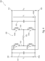
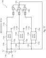
- FIG. 4 shows a schematic representation of a device for generating an AC voltage 400 with a "buck and step-up converter circuit” 430.
- the device for generating an AC voltage 400 has a first output voltage connection 410 and a second output voltage connection 420, for example by output voltage terminals, output voltage Plug contacts, output voltage screw connections, output voltage contacts or output voltage conductor tracks can be formed.
- An (output) AC voltage u WS can arise between the output voltage terminals 410, 420.
- the device for generating an AC voltage 400 has an input voltage feed 440 and a reference potential node 450a, 450b.
- the input voltage U E is applied between the input voltage supply 440 and the reference potential node 450a, 450b.
- the device for generating an AC voltage 400 has a “step-down and step-up converter circuit” 430 .
- this buck and boost converter 430 has an input capacitance 431 which is connected (coupled) between the input voltage feed 440 and the reference potential node 450a, 450b.
- the step-down and step-up converter 430 has a half-bridge circuit 432, which consists of two series-connected power switches 432a, 432b that are to be switched actively.
- Each of the two switches 432a, 432b of the half-bridge circuit 432 has an anti-parallel freewheeling diode.
- Active power switches can be, for example, metal-oxide-semiconductor field effect transistors (MOSFET) or bipolar transistors (BJT) or insulated gate bipolar transistors (IGBT).
- MOSFET metal-oxide-semiconductor field effect transistors
- BJT bipolar transistors
- IGBT insulated gate bipolar transistors
- the midpoint of the half-bridge circuit 432 is connected to a midpoint of a half-bridge circuit 434 via an inductance 433 (storage inductor, storage inductance).
- the half-bridge circuit 434 also has two power switches 434a, 434b that are to be switched actively.
- the two power switches 434a, 434b of the half-bridge circuit 434 each have an antiparallel freewheeling diode.
- the negative connection of the half-bridge circuit 434 is connected to the reference potential node 450a, 450b, the positive connection of the half-bridge circuit 434 is connected to connected to the output voltage terminal 410.
- An output capacitor 435 is connected in parallel with the half-bridge circuit 434 between the first output voltage connection 410 and the reference potential node 450a, 450b.
- the voltage u A ie the output voltage of the buck and boost converter 430, is present across this output capacitor 435.
- the device for generating an AC voltage 400 has an interconnection or a line connection that connects the input voltage feed 440 to the second output voltage connection 420 .
- the anodes of the freewheeling diodes (diodes, anti-parallel freewheeling diodes) of the low-lying power switches 432a, 434a of the half bridges 432, 434 are connected to the reference potential node 450a, 450b. With the power switch 432b high, the cathode of the diodes is connected to the input voltage supply 440 . The cathode of the diode of the high power switch 434b is connected to the positive terminal of the output capacitor 435 and the first output voltage terminal 410 .
- the cathodes of the diodes of the low-side switches 432a, 434a and the anodes of the diodes of the high-side switches 432b, 434b of a half-bridge 432, 434 are connected to one another and to the respective center point of a half-bridge 432, 434.
- the circuit Due to the soft-switching operation of the topology (e.g. with an input voltage of 400V and an output voltage of 200V...600V, the circuit generates a sinusoidal AC voltage of ⁇ 200V with the efficiency see Fig. 12b of DE102015219850 ) the switching losses are almost completely avoided.
- the output ground is not at 0 volts in relation to the reference potential node 450a, 450b, but at a constant potential and thus avoids displacement currents.
- the output voltage u A can be set in such a way that the output voltage shows a cosine-shaped potential curve which in turn has a mean value.
- This mean value can usefully be chosen to be the size of the input voltage U E , for example ⁇ 10%.
- a cosine/sine-shaped output voltage u WS between the first output voltage connection 410 and the second output voltage connection 420 can be achieved by this selection of the time curves.
- This sinusoidal potential course or the voltage curve can have a very low mean value, for example less than 10% of the amplitude of the sinusoidal potential curve (voltage curve).
- the device for generating an AC voltage 400 is suitable for supplying an AC voltage consumer with an (approximately) average-free AC voltage from a DC voltage source.
- a benefit can 4 be understood in a clear way. If the output voltage u A is considered, the counting direction of which is indicated by the corresponding arrow, it can be seen that the two antiparallel freewheeling diodes 434a, 434b of the half-bridge 434 are reverse-biased when the voltage is positive. With the same way of counting the output voltage u A but with a nominally negative voltage, the diodes 434a, 434b are forward-biased. Consequently, no significant negative voltage can be present across the output capacitor 435 . Thus, with a simple GS/GS converter 4 only one output voltage u A of one polarity can be generated.
- the second output voltage terminal 420 As a reference node for the AC output voltage, it is possible to generate a voltage that can be both positive and negative with respect to the second output voltage terminal 420 . Only then is it possible to generate an alternating voltage, ie a voltage with a positive and negative component. This possibility can also be transferred to the other comparative examples and exemplary embodiments.
- the comparative example according to 4 can be expanded to include an energy sink, which is connected between the first output voltage connection 410 and the second output voltage connection 420 or between the first output voltage connection 410 and the input voltage supply 440, so that a voltage at the energy sink has an AC voltage curve or an approximately mean-free AC voltage curve or a sinusoidal/cosinusoidal shape , means-free AC voltage curve corresponds.
- an arrangement can arise that corresponds to the circuit arrangement for generating an output AC voltage 200 2 can basically correspond.
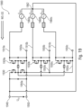
- figure 5 shows a schematic representation of a device for generating an AC voltage 500 with a "step-up and step-down converter circuit" 530.
- the device for generating an AC voltage 500 has a first output voltage connection 510 and a second output voltage connection 520, between which the AC voltage u WS is present .
- the device for generating an AC voltage 500 has an input voltage feed 540 and a reference potential node 550a, 550b.
- the input voltage U E is present between this reference potential node 550a, 550b and the input voltage supply line 540, which is therefore also present across the input capacitor 531.
- This input capacitor 531 is connected between the input voltage feed 540 and the reference potential node 550a, 550b.
- a coil 532 on the input side connects the positive terminal of the input capacitor 531 (i.e. also the input voltage supply 510) to the midpoint of a half-bridge circuit 533.
- the half-bridge circuit 533 in turn has two series-connected power switches 533a, 533b that are to be switched actively, each of which has an antiparallel freewheeling diode own.
- a capacitance 534 (coupling capacitor, intermediate storage capacitor) is connected in parallel with the half-bridge circuit 533 .
- a further half-bridge circuit 535 is connected in parallel with the coupling capacitor 534 .
- the half-bridge circuit 535 in turn also has two power switches 535a, 535b to be switched actively. Each of the power switches 535a, 535b to be switched actively in the half-bridge circuit 535 in turn has an antiparallel freewheeling diode.
- An output-side inductance 536 is connected to the middle point of the half-bridge circuit 535 , the second connection side of which is connected to a positive connection of an output capacitor 537 .
- This output capacitor 567 in turn is connected with the positive connection to the first output voltage connection 510 and with the negative connection to the reference potential node 550a, 550b.
- the reference potential node 550a, 550b connects the negative terminal of the input capacitor 531, the negative terminal of the half-bridge circuit 533, the negative terminal of the coupling capacitor 534, the negative terminal of the further half-bridge circuit 535 and the negative terminal of the output capacitor 537.
- the device for generating a AC voltage 500 an interconnection or line connection that connects the input voltage feed 540 to the second output voltage terminal 520 .
- the anodes of the freewheeling diodes (diodes, anti-parallel freewheeling diodes) of the low-lying power switches 533a, 535a of the half bridges 533, 535 are connected to the reference potential node 550a, 550b.
- the cathodes of the diodes are connected to the positive terminal of the coupling capacitance 534.
- the cathode of the diode of the low-side switch 533a and the anode of the diode of the high-side switch 533b are connected to one another and to the midpoint of the half-bridge 533 and to the second connection of the input-side inductance 532, respectively.
- the cathode of the diode of the low switch 535a and the anode of the diode of the high switch 535b are also connected to each other and to the midpoint of the half-bridge 535 and to the first terminal of the output-side inductor 536, respectively.
- the output voltage u A can be set in such a way that the output voltage u A in relation to the reference potential node 550a, 550b shows a cosine-shaped potential profile, which in turn has a mean value. It makes sense to select this mean value in the size of the input voltage U E .
- a sinusoidal output voltage u WS between the first output voltage connection 510 and the second output voltage connection 520 can be achieved by this choice of the time curves.
- This sinusoidal potential curve or voltage curve (related, for example, to the second output voltage connection 520) can have a very low mean value, for example less than 10% of the amplitude of the sinusoidal potential curve or voltage curve.
- the device for generating an AC voltage 500 is suitable for supplying an AC voltage consumer with an (approximately) average-free AC voltage from a DC voltage source.
- alternating voltage basically means a voltage that can have a positive and a negative polarity over time.
- the AC voltage can also be repeated periodically or averaged over one or more periods without an average value.
- the freedom from mean values can also only be approximately fulfilled, e.g. B. switching effects, control errors, etc. All the properties of the AC voltage mentioned can be transferred to the AC voltages of the other comparative examples and exemplary embodiments.
- the comparative example according to figure 5 can be expanded to include an energy sink, which is connected between the first output voltage connection 510 and the second output voltage connection 520 or between the first output voltage connection 510 and the input voltage supply line 540, so that a voltage at the energy sink has an AC voltage curve or an approximately mean-free AC voltage curve or a sinusoidal/cosinusoidal shape , means-free AC voltage curve corresponds.
- an arrangement can arise which can basically correspond to the circuit arrangement for generating an output AC voltage 200 .
- FIG. 6 shows a schematic representation of a device for generating an AC voltage 600 with an “unbalanced converter with input-side inductance circuit” 630 (English: “single ended primary inductance converter”, “SEPIC circuit”).
- the device for generating an AC voltage 600 with a "SEPIC circuit” 630 has a first output voltage connection 610 and a second output voltage connection 620 . The potential difference between these two connections is referred to as the output AC voltage or AC voltage u WS .
- the device for generating an AC voltage 600 has an input voltage feed 640 and a reference potential node 650a, 650b.
- the input voltage U E is present between the input voltage connections, ie the input voltage feed 640 and the reference potential node 650a, 650b.
- the device for generating an AC voltage 600 or the "SEPIC circuit” 630 has an input capacitor 631, which is connected between the input voltage feed 640 and the reference potential node 650a, 650b.
- the positive terminal of the input capacitor 631 is connected to an input inductor 632 .
- the second connection of the input inductance 632 is in turn connected to an active power switch 633 .
- This active power switch 633 has an antiparallel freewheeling diode (diode), the cathode of the diode of the power switch 633 is connected to the inductance 632 and the coupling capacitance 634 .
- the anode of the diode of the power switch 633 is connected to the reference potential node 650a, 650b.
- the negative connection of the active power switch 633 is connected to the reference potential node 650a, 650b.
- the positive connection of the active power switch 633 and the second connection of the input inductance 632 are connected to a coupling capacitance 634 (capacitor).
- This coupling capacitance 634 is in turn connected to the first connection of an inductance 635, whose second connection is in turn connected to the reference potential node 650a, 650b.
- the second connection of the coupling capacitance 634 and the first connection of the inductance 635 are in turn connected to an active power switch 636 .
- This active power switch 636 in turn has a diode (anti-parallel freewheeling diode).
- the anode of the diode of the power switch 636 is connected to the coupling capacitance 634 and the inductance 635 .
- the cathode of the power switch 636 is connected to the positive terminal of the output capacitor 637 and the output voltage terminal 610 .
- the second connection of the active power switch 636 is connected to a positive connection of an output capacitance 637 .
- the positive connection of the output capacitance 637 is connected to the active power switch 636 and the first output voltage connection 610, the negative connection of the output capacitance 637 is connected to the reference potential node 650a, 650b.
- the output voltage u A is present across this output capacitance 637 .
- the device for generating an AC voltage 600 has a connection/interconnection which connects the input voltage feed 640 to the second output voltage connection 620 .
- the output voltage u A which is present across the output capacitance 637, can be set to vary over time.
- a sinusoidal curve of the voltage (with a suitable mean value) across the output capacitance 637 it can be achieved that a sinusoidal, mean-free voltage curve (or approximately a mean-free voltage curve) is present between the terminals or connections 610, 620.
- an AC voltage u WS which is present between the first output voltage connection 610 and the second output voltage connection 620, can be generated from a DC voltage U E that is present between the input voltage supply 640 and the reference potential node 650a, 650b.
- a switching load reduction is possible for a switching load reduction to be achieved by suitable activation of the active power switches 633, 636 and/or by suitable switching load-relief interconnection of the active power switches 633, 636.
- This switching relief allows the circuit breakers to be switched on and off softly. This can improve the electromagnetic compatibility and/or the switching power loss.
- the comparative example according to 6 can be expanded to include an energy sink, which is connected between the first output voltage connection 610 and the second output voltage connection 620 or between the first output voltage connection 610 and the input voltage supply 640, so that a voltage at the energy sink has an AC voltage curve or an approximately mean-free AC voltage curve or a sinusoidal/cosinusoidal shape , means-free AC voltage curve corresponds.
- an arrangement can arise that corresponds to the circuit arrangement for generating an output AC voltage 200 2 can basically correspond.
- FIG. 7 shows a schematic representation of a device for generating an alternating voltage 700 with a "zeta circuit" 730.
- the so-called “zeta circuit” 730 corresponds to that in the comparative example 6 presented DC voltage / DC voltage converter circuit 630 related.
- the device for generating an AC voltage 700 has a first output voltage connection 710 and a second output voltage connection 720, via which the AC voltage or AC output voltage u WS is present. Furthermore, the device for generating an AC voltage 700 has an input voltage feed 740 and a reference potential node 750a, 750b.
- the input voltage U E is present between the input voltage connections, ie the input voltage feed 740 and the reference potential node 750a, 750b.
- the input capacitance 731 is connected between the input voltage feed 740 and the reference potential node 750a, 750b.
- the input voltage U E is in turn present across this input capacitance 731 .
- the positive connection of the input capacitance 731 is connected to a active power switch 732 connected, the negative terminal of the input capacitance 731 is connected to the reference potential node 750a, 750b.
- the active power switch 732 is connected to an inductance 733 and a coupling capacitance 734 at its second connection.
- the active power switch 732 includes a diode (anti-parallel freewheeling diode).
- the cathode of the diode of the power switch 732 is connected to the input capacitor 731 and the input voltage supply 740 .
- the anode of the diode power switch 732 is connected to the inductance 733 and the coupling capacitance 734 .
- the inductance 733 is connected at its first connection to the active power switch 732 and the first connection of the coupling capacitance 734 (coupling capacitor, capacitor).
- the second connection of the inductor 733 is connected to the reference potential node 750a, 750b.
- the second connection of the coupling capacitance 734 is in turn connected to an active power switch 735 and an inductance 736 .
- the negative connection of the active power switch 735 is connected to the reference potential node 750a, 750b and the power switch 735 has an associated diode (anti-parallel freewheeling diode).
- the cathode of the diode of the power switch 735 is connected to the coupling capacitance 734 and the first connection of the inductance 736, the anode of the associated diode of the power switch 735 is connected to the reference potential node 750a, 750b.
- the (output) inductance 736 is connected to the coupling capacitance 734 and the active power switch 735 at its first connection; the second connection of the inductance 736 is connected to the output capacitance 737 and the first output voltage connection 710 .
- the output capacitance 737 is in turn connected to the first output voltage connection 710 at its positive connection and to the reference potential node 750a, 750b at its negative connection.
- the output voltage u A is present across the output capacitance 737 .
- the device for generating an AC voltage 700 has an interconnection or a line connection or a conductor connection, which connects the input voltage feed 740 to the second output voltage connection 720 .
- the output voltage u A which is present across the output capacitance 737, can be set to vary over time.
- a sinusoidal waveform of the voltage across the output capacitance 737 can be achieved that a sinusoidal, mean value-free potential curve at the terminals 710, 720 is present.
- This can be achieved that from a DC voltage U E that is present between the input voltage supply 740 and the reference potential node 750a, 750b, an AC voltage u WS is generated that is present between the first output voltage terminal 710 and the second output voltage terminal 720.
- the comparative example 7 can be achieved by a suitable control of the active power switches 732, 735 that the output voltage u A assumes a sinusoidal curve.
- U E is the input voltage of the DC/DC converter.
- û is the amplitude of the sinusoidal voltage and satisfies the condition û ⁇ U E .
- the voltage difference between the output of the DC/DC converter, ie the voltage u A , and the input of the DC/DC converter, ie the voltage U E makes up the AC voltage u WS .
- the comparative example according to 7 be switched softly.
- the switching losses are almost completely avoided thanks to the soft-switching operation of the topology.
- Large voltage changes at the output are also reduced and thus harmonic loading (harmonic loading) is reduced.
- the output ground is not at 0V, but at a constant potential that approximately corresponds to the potential of the input voltage supply, thus avoiding displacement currents. If present, these displacement currents would have to be reduced by more complex filters.
- One advantage of the aforementioned devices for generating an AC voltage 100 to 700 is that the output mass remains at a constant voltage level and, as a result, unwanted displacement currents do not have to be reduced by expensive filters.
- a further advantage that all of the aforementioned devices for generating an AC voltage and the circuit arrangement for generating an output AC voltage 100 to 700 can have is that there are high voltage changes at the power semiconductors can be avoided and an associated high generation of harmonics. This low harmonic generation does not therefore have to be reduced by large output filters.
- the comparative example according to 7 can be expanded to include an energy sink, which is connected between the first output voltage connection 710 and the second output voltage connection 720 or between the first output voltage connection 710 and the input voltage supply line 740, so that a voltage at the energy sink has an AC voltage curve or an approximately mean-free AC voltage curve or a sinusoidal/cosinusoidal shape , means-free AC voltage curve corresponds.
- an arrangement can arise that corresponds to the circuit arrangement for generating an output AC voltage 200 2 can basically correspond.
- the method 800 includes operating 810 a DC-DC converter.
- an input voltage is present between an input voltage feed and a reference potential node.
- an output voltage of the DC-DC converter is generated in such a way that an output node at times has a potential that is more positive than the potential present at the input voltage supply.
- the DC-to-DC converters are operated in such a way that the output node temporarily has a potential which is more negative than the potential present at the input voltage supply.
- the method 800 further includes tapping 820 the AC output voltage for the energy sink between the output node and the input voltage supply.
- the output AC voltage is tapped 820 in such a way that the potential difference between the input voltage feed and the output node corresponds to a voltage present at the energy sink.
- This operating method 800 can also be used to generate an AC output voltage for an energy sink.
- This method can nevertheless be compared with the comparative examples Figures 1 to 7 presented devices for generating an AC voltage and circuit arrangements for generating an output AC voltage 100 - 700 are combined.
- the other comparative examples mentioned above can also be combined with the method for generating an alternating output voltage.
- the method can also be supplemented by the features and functionalities explained herein in relation to the devices according to the invention.
- FIG. 9 shows a schematic representation of an inverter 900 for generating an AC voltage from a DC voltage.
- the inverter has an input DC voltage connection 910, which is designed to have an input DC voltage applied to it.
- the DC voltage can originate, for example, from a DC voltage source, such as, for example, a plurality of photovoltaic cells (connected, for example, in series), a DC voltage energy store, or a rectified AC voltage.
- the inverter also has a device for generating an AC voltage 920, the device for generating an AC voltage 920 (e.g. as in the devices for generating an AC voltage 100, 300a, 400, 500, 600, 700, 1020) generating a DC voltage - DC/DC converters (e.g. such as DC/DC converters 130, 230, 330, 430, 530, 630, 730).
- the DC-DC converter may be configured to generate an output voltage based on an input voltage.
- the input voltage is present between an input voltage feed 922 and a reference potential node 924 .
- the DC voltage-DC voltage converter is designed to generate the output voltage in such a way that a first output voltage connection 926 temporarily has a potential that is more positive than the potential present at the input voltage feed 922 . Furthermore, the DC voltage-DC voltage converter is designed in such a way that the first output voltage connection 926 temporarily has a potential that is more negative than the potential present at the input voltage feed 922 . Furthermore, the second output voltage connection 928 is coupled to the input voltage feed 922 .
- the inverter 900 also has an AC output voltage connection 930 which is designed to provide an AC output voltage.
- the inverter is designed in such a way that the input voltage supply 922 and the reference potential node 924 of the device for generating an AC voltage 920 z. B. are coupled with low impedance to two contacts of the DC input voltage connection 910 . Furthermore, the first output voltage connection 926 and the second output voltage connection 928 of the device for generating an AC voltage 920 with contacts z. B. for connection of a load of the incoming AC voltage terminal 930 is coupled.
- the inverter 900 for generating an AC voltage from a DC voltage is thus designed to convert a DC voltage that is connected to the input DC voltage connection 910 into an output AC voltage that is provided at the output AC voltage connection 930 .
- An AC voltage load can thus be operated with the inverter 900 from a DC voltage source.
- This AC voltage load can represent a consumer, a load or possibly also an electrical supply network. In general, the AC voltage load can also be described by an energy sink.
- This system 900 can be equipped with the devices for generating an AC voltage and circuit arrangements for generating an output AC voltage, which are shown in the comparative examples according to Figures 1 to 7 were presented can be combined. Furthermore, the other aforementioned comparative examples presented in the summary of the invention can also be combined with the system 900. The system can otherwise be supplemented by the features and functionalities explained herein in relation to the devices according to the invention.
- FIG. 10 shows a schematic representation of an energy storage device 1000 for providing an AC voltage using a DC voltage energy store 1010, wherein the energy storage device 1000 has a DC voltage energy store 1010, which is designed to store energy and to provide the energy as DC voltage.
- a deviation of the DC voltage from a desired value can occur to a limited extent, for example when the energy is removed.
- the energy storage device 1000 has a device for generating an AC voltage 1020 (e.g. as in the devices for generating an AC voltage 100, 300a, 400, 500, 600, 700, 920).
- the device for generating an AC voltage 1020 has a DC-DC converter (z. B. like the GS / GS converter 130, 230, 330, 430, 530, 630, 730), which is designed to based on an input voltage, for example the DC voltage provided by the DC voltage energy storage source 1010, to generate an output voltage, the input voltage being present between an input voltage feed 1022 and a reference potential node 1024.
- a DC-DC converter z. B. like the GS / GS converter 130, 230, 330, 430, 530, 630, 730
- the DC voltage-DC voltage converter is designed to generate the output voltage in such a way that a first output voltage connection 1026 temporarily has a potential that is more positive than the potential present at the input voltage feed 1022 . Furthermore, the DC-DC converter is designed to generate the output voltage in such a way that the first output voltage connection 1026 temporarily has a potential that is more negative than the potential present at the input voltage feed 1022 . Furthermore, the second output voltage connection 1028 is coupled to the input voltage feed 1022, for example directly, statically, in a low-impedance, low-impedance, low-inductance manner.
- the energy storage device 1000 has an output AC voltage connection 1030 which is designed to provide an output AC voltage.
- the DC energy storage device 1010 is included in the energy storage device 1000 the input voltage supply 1022 and the reference potential node 1024 of the device for generating an AC voltage 1020 coupled.
- This energy storage device or energy storage connection 1000 can be used, for example, in the field of hybrid/electric vehicles.
- the direct voltage energy store 1010 can be implemented, for example, by a chemical direct voltage energy source such as an accumulator.
- a chemical direct voltage energy source such as an accumulator.
- DC voltage energy stores are also conceivable, which can deliver stored energy in the form of DC voltage.
- the DC voltage energy store can release the stored energy, which can be stored, for example, in chemical form or as rotational energy, in the form of electrical energy or in the form of electrical power over a period of time.
- the electrical voltage can only deviate to a negligible extent from a mean voltage, for example within a high-frequency period of the GS/GS converter or a few high-frequency periods of the GS/GS converter.
- the energy source can thus be viewed as an approximately constant voltage source or direct voltage source or direct voltage energy store.
- This system 1000 can be equipped with the devices for generating an AC voltage and circuit arrangements for generating an output AC voltage, which are shown in the comparative examples according to FIG Figures 1 to 7 were presented can be combined. Furthermore, the other aforementioned comparative examples presented in the summary of the invention can also be combined with the system 100. The system can also be supplemented by the features and functionalities explained herein in relation to the devices according to the invention.
- the exemplary embodiment shows a possible embodiment of a three-phase inverter that is based on the solution according to the invention.
- FIG. 12 12 shows an illustration of a three-phase inverter 1200 according to a comparative example.
- the suffixes a, b, c assign the respective elements to one of the three phases, which can thus be referred to as phase a, phase b and phase c.
- the three-phase inverter 1200 has three DC/DC converters 1230a, 1230b, 1230c.
- An input voltage supply 1240a, 1240b, 1240c is assigned to each of these GS/GS converters 1230a, 1230b, 1230c.
- These input voltage feeds 1240a, 1240b, 1240c are connected together to form the (superordinate) input voltage feed 1240.
- the three-phase inverter 1200 has three reference potential nodes 1250a, 1250b, 1250c. These reference potential nodes 1250a, 1250b, 1250c can also be combined with the (superordinate) reference potential node 1250 to form a "large" reference potential node. In order to point out the lack of galvanic isolation of the GS/GS converters 1230a, 1230b, 1230c, the reference potential nodes are also shown on the “output side” of the GS/GS converters 1230a, 1230b, 1230c as the reference potential nodes 1250a, 1250b, 1250c.
- the GS/GS converters 1230a, 1230b, 1230c are designed, for example, such that they provide a positive output voltage (related to the respective reference potential node 1250a, 1250b, 1250c) at the output node 1210a, 1210b, 1210c in a respective first time segment and so that they provide a negative output voltage (related to the respective reference potential node 1250a, 1250b, 1250c) at the output node 1210a, 1210b, 1210c in a respective second period of time.
- a load 1260a, 1260b, 1260c is connected between the respective output nodes 1210a, 1210b, 1210c and a neutral point 1262 (or thus between the respective output nodes 1210a, 1210b, 1210c and the input voltage supply 1240).
- This load can generally be an energy sink, too a three-phase network would be conceivable at this point, or a three-phase motor.
- the z. B. in relation to the comparative example according to 2 and the energy sink 260 have been named.
- the connections of the three-phase energy sink 1260a, 1260b, 1260c can, for example, be brought together on one connection side in a star point 1262, which in turn is coupled to the input voltage feed 1240.
- multiple single-phase energy sinks can also be separately coupled to the (superordinate) input voltage supply 1240 . It would also be possible to couple these to the input voltage leads 1240a, 1240b, 1240c.
- the step-up and step-down function can in turn be achieved by suitable control of the GS/GS converters 1230a, 1230b, 1230c.
- suitable control of the GS/GS converters 1230a, 1230b, 1230c e.g. B. also a phase-shifted control of the GS / GS converter 1230a, 1230b, 1230c be useful.
- a three-phase inverter 1300 is shown, which has a comparable structure to the inverter 1200.
- a respective "general" GS/GS converter 1230a, 1230b, 1230c was replaced by a “concrete” example of a “buck and boost converter circuit” 1330a, 1330b, 1330c, the other topologies of the aforementioned (single-phase) comparative examples (such as e.g., the "boost and buck circuit", the "SEPIC circuit”, etc.) can also be used.
- the input voltage leads 1340, 1340a, 1340b, 1340c and the reference potential nodes 1350, 1350a, 1350b, 1350c are designed analogously to the inverter 1200, for example.
- the energy sink 1360a, 1360b, 1360c corresponds to the energy sink 1260a, 1260b, 1260c.
- the star point 1362 also corresponds in principle to the star point 1262.
- the fact that the energy sink 1360a, 1360b, 1360c is connected between a respective output node 1310a, 1310b, 1310c and the input voltage supply 1340 is again important. This makes it possible to convert the DC voltage that is present between the input voltage supply 1340 and the reference potential node 1350 into a (three-phase) AC voltage that is (approximately) present at the respective phases of the energy sink 1360a, 1360b, 1360c.
- the inverter 1400 has an arrangement similar to that of the comparative example 13 can be derived.
- the phase of the energy sink 1460a, 1460b, 1460c is connected between a respective output node 1410a, 1410b, 1410c and the input voltage supply 1440, as in the previous comparative examples.
- a sinusoidal AC voltage which also has, for example, a phase offset between the respective AC voltages, advantageously z. B. has a phase shift of 120 °.
- the GS/GS converters can be formed from a combination of a front (input-side) circuit part 1330 with the three rear (output-side) circuit parts 1330a, 1330b, 1330c.
- the inductances 1333a, 1333b, 1333c (coils, chokes) can also have a decoupling function between the three phases.
- a clocking or a clocking frequency of the front circuit part 1330 can also be selected to be significantly higher than a clocking of the three rear circuit parts 1330a, 1330b, 1330c.
- a clock frequency of the front circuit part 1330 can be selected which corresponds approximately to three times the clock frequency of the three rear circuit parts 1330a, 1330b, 1330c.
- the front circuit part 1330 can be used, for example, as a buck converter and that the three rear circuit parts 1330a, 1330b, 1330c z. B. can be used as a step-up converter.
- the three rear circuit parts 1330a, 1330b, 1330c z. B. can be used as a step-up converter.
- other functionalities would also be conceivable, which can be achieved, for example, by a suitable control or selection of the component values.
- energy sinks (1260a, 1260b, 1260c; 1360a, 1360b, 1360c; 1460a, 1460b, 1460c) are shown as components. These energy sinks can be dispensable functionally and thus represent only one example of a possible embodiment. Accordingly derived from this would be conceivable, which have no energy sinks, but instead provide a three-phase AC voltage system (e.g. a symmetrical, three-phase AC voltage system (AC system), e.g. with a phase offset of 120°) at several connection terminals.
- the connection terminals can have different designs. For example, screw connections or plug-in connections or clamp connections or also a mechanical connection and electrical contacting, which is implemented by different devices in each case, would be conceivable.
- the coupling can thus also be realized by one of the other GS-GS converters, but this should advantageously be formed in such a way that the neutral point (or a corresponding connection or corresponding connections of the (three-phase) energy sink) has a potential which is approximately the potential corresponds to the input voltage supply.
- Figure 15a Figures 16a and 16b show three different comparative examples. All clarify the concept of using the solution according to the invention for rectifying an AC voltage.
- Figure 15b shows the (schematic, exemplary) time curves of three voltages, which also illustrate the concept of using the solution according to the invention as a rectifier circuit.
- Figure 15a shows a representation of a circuit for generating a DC voltage 1500a from an AC voltage source 1515, the circuit z. B. with the circuit 300a in 3 is comparable.
- the circuit for generating a DC voltage 1500a has an AC voltage feed 1510, 1520, which is formed by the two terminals (contacts or the like), the first (input) AC voltage terminal 1510 and the second (input) AC voltage terminal 1520.
- These contacts/connections/terminals can be formed in different ways. Screw, clamp, plug-in connections can be just as conceivable as crimped connections. It can be said in general terms that, in addition to electrical contacting, mechanical attachment is usually desired. The actual execution can be very different.
- the AC voltage supply 1510, 1520 is supplied with a sinusoidal AC voltage, for example, which is symbolized by an AC voltage source 1515.
- This (input) AC voltage can have a mean value that is not equal to zero.
- the circuit for generating an AC voltage 1500a has a DC-DC converter 1530 (GS/GS converter, DC/DC converter).
- This GS-GS converter 1530 can be designed in such a way that it generates a DC voltage between a first (output) DC voltage connection 1540 and a second (output) DC voltage connection 1550, with the GS-GS converter 1530 being designed in such a way that this generates the magnitude of the DC voltage U GS , for example, in such a way that it approximately corresponds to the mean value of the (input) AC voltage 1515 .
- the difference to the aforementioned comparative examples, which generate an AC voltage from a DC voltage is the energy flow direction.
- the power flow direction (energy flow direction) is according to the comparative example Figure 15a viewed from right to left and indicated with an arrow labeled WS/GS. With the solution, it may thus be possible to set an energy flow direction, ie to use the same embodiment of the solution for rectification and also for inversion.
- Figure 15b shows a schematic representation 1500b of the time course of the three voltages u WS 1572, U GS+ 1574 and U Gs- 1576.
- the representation 1500b has an abscissa 1570, which represents a time axis, and also an ordinate 1571, which represents a voltage axis.
- the representation 1500b shows the three voltages, the (input) AC voltage 1572 ( u WS ), the positive (output) DC voltage 1574 (or the positive (output) potential) ( U GS+ ) and the negative output DC voltage 1576 (or the negative (output) potential) ( U GS- ).
- the concept of the solution according to the invention can thus be understood from the time curves.
- a potential of the AC voltage u WS for example the potential of the second AC voltage connection 1520, is coupled to the first (output) DC voltage connection 1540.
- the potential of the AC voltage u WS selected for this can advantageously be such that the potential has an approximately static (time-invariant, fixed, fixed) potential ( u GS+ ) with respect to an (electrical) mass or with respect to earth.
- the GS-GS converter 1530 is designed in such a way that it converts the (time-varying) potential present at the first AC voltage connection 1510 in such a way that the second output DC voltage connection 1550, which can correspond to a reference potential node 1550 of the GS-GS converter 1530, has an approximately time-invariant potential ( u GS- ).
- a DC voltage U GS can thus be made available between the first output DC voltage connection 1540 and the second output DC voltage connection 1550 .
- the time course of the AC voltage u WS 1572 is sinusoidal and (relative to the potential U GS- ) has a mean value which is not equal to zero.
- the time profile of the (output DC) voltage (or the potential) U GS+ 1574 is approximately constant (related to the potential U GS- ) and corresponds (approximately) to the mean value of the AC voltage u WS .
- the time course of the potential u GS- is also (approximately) constant in the representation and is shown as (approximately) zero. This results in the output DC voltage U GS .
- This output DC voltage is therefore the potential difference between U GS+ and U GS- .
- a DC output voltage can thus be generated from an AC voltage source using the solution according to the invention.
- the circuit 1500 can also be understood in such a way that the DC voltage-DC voltage converter 1530 generates or regulates a voltage U GS between the first input voltage connection 1540 and the second input voltage connection 1550 .
- a first connection of the AC voltage source 1515 to the first AC voltage connection 1510 and by connecting a second connection of the AC voltage source 1515 to the second AC voltage connection 1520 it can be achieved (for example by suitable dimensioning) that in stationary operation of the circuit 1500a the Potential at the first AC voltage connection is always positive (in other embodiments always negative) compared to the potential at the second output DC voltage connection, i.e. it does not cross the "reference potential" of the DC voltage-DC voltage converter".
- Input voltage of the DC-DC converter related to the reference potential of the DC-DC converter (i.e. related to the potential of the potential rail, which is connected to both the input circuit of the DC-DC converter and the output circuit of the DC-DC converter with low resistance coupled), never to zero.
- the DC voltage-DC voltage converter can receive an input voltage which differs from zero at any point in time (for example during an entire period of the AC voltage).
- the DC-DC converter can achieve power transmission at all times (for example, during an entire cycle of the AC voltage).
- Figures 16a and 16b show two further comparative examples, also for generating a DC voltage U GS from an AC voltage source 1615a, 1615b.
- the solution is implemented with a "step-down and step-up converter circuit".
- the circuit for generating a DC voltage 1600a from an AC voltage source 1615a has a first AC voltage connection 1610a and a second AC voltage connection 1620a.
- the AC voltage source 1615a is connected to these AC voltage contacts 1610a, 1620a, or the circuit for generating a DC voltage 1600a can be supplied with an AC voltage ( u WS ) via the AC voltage terminals 1610a, 1620a.
- one terminal of the AC voltage source 1615a is coupled to the first AC voltage terminal 1610a.
- Another connection of the AC voltage source 1615a is coupled to the second AC voltage connection 1620a.
- This second AC voltage connection 1620a is in turn coupled to the first (output) DC voltage connection 1640a.
- This can e.g. B. statically, directly, happen with low resistance. It is important that the coupling is implemented in such a way that the potential of the coupled connection of the AC voltage source 1615a approximately corresponds to the potential of the first (output) DC voltage connection 1640a.
- the circuit for generating a DC voltage 1600a has a GS-GS converter 1630a, which corresponds to a “buck and boost converter circuit” in the comparative example shown.
- This first output DC voltage connection is separated from the continuous reference potential or reference potential node of the DC voltage-DC voltage converter or is connected to the continuous reference potential of the DC voltage-DC voltage converter via one or more switches not directly connected. Rather, a reference potential node of the DC-DC converter 1630a may correspond to the second (output) DC voltage terminal 1650a.
- This can, for example, have a fixed potential that does not change over time, which is denoted by U GS- in the illustration.
- a direct voltage U GS is thus made available with the potential of the first (output) direct voltage connection 1640a U GS+ .
- This DC voltage U GS thus corresponds to a potential difference between the two (output) DC voltage connections 1640a, 1650a.
- the GS/GS converter 1630a can be designed in such a way that the GS/GS converter 1630a has no galvanic isolation, or that at least the power-transmitting part has no galvanic isolation (input circuit and output circuit are both low-impedance to the reference potential node tied together).
- the circuit 1600a has a first input AC voltage connection 1610a and an "explicit" second input AC voltage connection 1620a, which in turn has e.g. B. can be connected to a line with the first output DC voltage terminal 1640a.
- the AC voltage source 1615b is connected between two nodes (or a node and a terminal). On one side to a first input AC voltage node 1610b and on the other side to the node of the first output DC voltage connection (or to the output DC voltage connection 1540b).
- the two different comparative examples are based on the idea of the solution according to the invention.
- the power flow direction is selected from an AC voltage source 1615a, 1615b to a (possible) DC voltage consumer, while in the corresponding comparative example 400 a power flow direction is selected from a DC voltage source to a (possible) AC voltage load.
- the solution according to the invention thus permits both functionalities.
- This direction of power flow is indicated by an arrow labeled WS-GS.
- the comparative example is a device for generating a DC voltage 1500, 1600a from an input AC voltage.
- the DC voltage is present between a first output DC voltage connection 1540, 1640a and a second output DC voltage connection 1550, 1650a.
- the device has a DC voltage-DC voltage converter 1530, 1630a, which is designed to generate the DC voltage based on a first potential of the input AC voltage and on a potential of the second output DC voltage connection 1550, 1650a (or based on the time-varying potential difference).
- the first potential of the AC input voltage is present at a first AC input voltage terminal 1510, 1610a
- the second potential of the AC input voltage is present at a second AC input voltage terminal 1520, 1620a.
- the DC voltage-DC voltage converter 1530, 1630a is also designed to generate the DC voltage in such a way that the first output DC voltage connection 1540, 1640a has a potential which is approximately constant in relation to the second output DC voltage connection 1550, 1650a.
- the second input AC voltage connection 1520, 1620a is coupled to the first output DC voltage connection 1540, 1640a.
- the comparative example of the circuit arrangement for generating a DC output voltage 1600b from an AC voltage source 1615b has a first DC output voltage connection 1640b and a second DC output voltage connection 1650b, between which the DC output voltage is present. Furthermore, the circuit arrangement for generating an output DC voltage has a DC voltage-DC voltage converter 1630b.
- the DC voltage-DC voltage converter 1630b is designed to generate the output DC voltage based on a first potential of the AC voltage source 1615b and a potential of the second output DC voltage connection 1650b.
- the DC voltage-DC voltage converter 1630b is designed to generate the output DC voltage in such a way that the first output DC voltage connection 1640b has a potential which is approximately constant in relation to the second output DC voltage connection 1650b. Furthermore, the first potential of the AC voltage source 1615b is present at an input AC voltage node 1610b and a second potential of the AC voltage source 1615b is present at the first output DC voltage connection 1640b, so that the potential difference between the first output DC voltage connection 1640b and the input AC voltage node 1610b corresponds to a voltage output by the AC voltage source 1615b.
- An approximately constant potential can mean, for example, a maximum deviation of 5% from the mean value of the potential (or the voltage or the potential difference).
- 17 , 18 and 19 show comparative examples and an exemplary embodiment of the solution according to the invention for generating a DC voltage from a three-phase AC voltage (for example a three-phase AC voltage system, or also a symmetrical, three-phase AC voltage system).
- the circuit for generating a DC voltage 1700 from a three-phase AC voltage can be used as in 17 shown.
- the circuit for generating a DC voltage 1700 can be viewed as being divided into three phases or circuit paths, or the circuit for generating a DC voltage 1700 can be made up of three single-phase rectifiers, such as e.g. Am 15 or 16 shown, put together.
- the three phases a, b and c are structured in a way that is comparable to one another.
- the (three-phase) AC voltage source 1760a, 1760b, 1760c is connected at its three phases to the corresponding (input) AC voltage terminals 1710a, 1710b, 1710c of the DC/DC converters 1730a, 1730b, 1730c.
- the three phases of the three-phase AC voltage source are brought together at a star point 1762 on their other connection side.
- the neutral point 1762 is coupled to a first (output) DC voltage connection 1740 .
- a controller and/or regulator can be designed such that the potential of the star point 1762 approximately corresponds to the potential of the first output DC voltage connection 1740 .
- the output DC voltage U GS is made available.
- the direction of energy flow is indicated by the arrow labeled WS/GS.
- This energy flow direction is not solely predetermined by the circuit, but can be a consequence of the (three-phase) AC voltage source 1760a, 1760b, 1760c. If the AC voltage source 1760a, 1760b, 1760c is replaced by a (three-phase) load and if a DC voltage is applied to the (output) DC voltage connections 1740, 1750 (e.g. by a DC voltage source), the circuit can also be used as a (three-phase) inverter .
- a three-phase rectifier 1800 is shown, e.g. B. can be based on the concept of the three-phase rectifier 1700.
- the GS-GS converters 1830a, 1830b, 1830c are constructed as "buck and boost converter circuits". Many elements of rectifier 1700 can be found in rectifier 1800.
- a three-phase AC voltage source 1860a, 1860b, 1860c provides a three-phase (symmetrical) AC voltage system (eg with a phase offset between the individual phases of 120°).
- the respective first connection side of the three phases of the three-phase AC voltage source 1860a, 1860b, 1860c is coupled to a respective first (input) AC voltage connection 1810a, 1810b, 1810c of the GS/GS converter 1830a, 1830b, 1830c.
- the second connection sides of the three phases of the three-phase AC voltage source 1860a, 1860b, 1860c are connected to form a star point 1862.
- the star point 1862 is coupled to a first output DC voltage connection 1840, or to a respective first (output) DC voltage connection 1840a, 1840b, 1840c of the GS/GS converters 1830a, 1830b, 1830c.
- the reference potential nodes 1850a, 1850b, 1850c of the GS/GS converters 1830a, 1830b, 1830c are also coupled or connected to one another and form a common reference potential node 1850, which can also be the second (output) DC voltage connection 1850, for example.
- a connection of the star point 1862 to the first (output) AC voltage connection 1840 can be omitted in a symmetrical AC voltage system of the three-phase AC voltage source 1860a, 1860b, 1860c.
- the coupling of the star point 1862 (or the three-phase AC voltage sources 1860a 1860b, 1860c) to the first (output) DC voltage connection 1840 can be realized through one of the phases. Nevertheless, it can be advantageous that the potential of the star point 1862 corresponds approximately to the potential of the first output DC voltage connection 1840.
- a three-phase rectifier 1900 is shown.
- This three-phase rectifier 1900 has a number of similarities with the three-phase rectifier 1700 and the three-phase rectifier 1800. All three rectifiers are powered by a three-phase AC power source (in 19 : the three-phase AC voltage source 1960a, 1960b, 1960c). Furthermore, there are the correspondences of the first (input) AC voltage connections 1910a, 1910b, 1910c, the star point 1962, the first (output) DC voltage connection 1940 and the second (output) DC voltage connection 1950.
- the second output DC voltage connection 1950 can be connected to a reference potential node of a ( or more) DC-DC converters 1930, 1930a, 1930b, 1930c.
- the GS/GS converters 1930, 1930a, 1930b, 1930c of the GS-GS converters cannot be "concretely” identified herein as a "classic”"buck and boost converter circuit". become. Nevertheless, the GS-GS converters 1930, 1930a, 1930b, 1930c (or combinations of the GS/GS converters) should be able to master step-up and step-down conversion in order to convert a desired DC voltage, for example at the level of an average value of the AC voltage at the (output) To provide direct voltage connections in 1940, 1950.
- the rectifier circuit 1900 can enable a power flow direction from an AC voltage source to a DC voltage load, but also from a DC voltage source to an AC voltage load.
- the power flow direction is sensibly from the source to a (possible) load specified.
- the load can be connected to the DC output terminals 1940, 1950 and thus be supplied by an AC (three-phase) voltage source 1960a, 1960b, 1960c.
- a three-phase rectifier device for generating a DC voltage 1700, 1800, 1900 which is between a first output DC voltage connection 1740, 1740a, 1740b, 1740c, 1840, 1840a, 1840b, 1840c, 1940, 1940a, 1940b, 1940c and a second output DC voltage terminal 1750, 1750a, 1750b, 1750c, 1850, 1850a, 1850b, 1850c, 1950, 1950a, 1950b, 1950c can be created.
- the three-phase rectifier device 1700, 1800, 1900 has a plurality of DC-DC converters 1730a, 1730b, 1730c, 1830a, 1830b, 1830c, 1930, 1930a, 1930b, 1930c, which are designed to based on a first potential of a respective Phase of a three-phase AC voltage and a potential of the second output DC voltage terminal 1750, 1750a, 1750b, 1750c, 1850, 1850a, 1850b, 1850c, 1950, 1950a, 1950b, 1950c to generate a respective output voltage.
- the first potential of the respective phase of the three-phase AC voltage is at a respective input AC voltage connection 1710a, 1710b, 1710c, 1810a, 1810b, 1810c, 1910a, 1910b, 1910c and a second potential of the respective phase of the three-phase AC voltage is at a neutral point 1762, 1862, 1962 at.
- the DC-DC converters 1730a, 1730b, 1730c, 1830a, 1830b, 1830c, 1930, 1930a, 1930b, 1930c are designed to generate the respective output voltage in such a way that the first output DC voltage connection 1740, 1740a, 1740b, 1740 c, 1840, 1840a, 1840b, 1840c, 1940, 1940a, 1940b, 1940c with respect to the second DC output terminal 1750, 1750a, 1750b, 1750c, 1850, 1850a, 1850b, 1850c, 1950, 1950a , 1950b, 1950c has a potential that (at least in a steady state operation) is approximately constant.
- star point 1762, 1862, 1962 is coupled to the first output DC voltage terminal 1740, 1740a, 1740b, 1740c, 1840, 1840a, 1840b, 1840c, 1940, 1940a, 1940b, 1940c.
- This exemplary embodiment shows a further possible configuration of the solution according to the invention; another configuration is explained below.
- a three-phase rectifier circuit for generating an output DC voltage 1700, 1800 1900 between a first output DC voltage terminal 1740, 1740a, 1740b, 1740c, 1840, 1840a, 1840b, 1840c, 1940, 1940a, 1940 b, 1940c and a second DC output terminal 1750, 1750a, 1750b, 1750c, 1850, 1850a, 1850b, 1850c, 1950, 1950a, 1950b, 1950c from a three-phase AC voltage source 1760a, 1760b, 1760c, 186 0a, 1860b, 1860c, 1960a, 1960b, 1960c to provided.
- the three-phase rectifier circuit 1700, 1800, 1900 has a plurality of DC-DC converters 1730a, 1730b, 1730c, 1830a, 1830b, 1830c, 1930, 1930a, 1930b, 1930s, which are designed to based on a first potential of a respective Phase of the three-phase AC voltage source 1760a, 1760b, 1760c, 1860a, 1860b, 1860c, 1960a, 1960b, 1960c and a potential of the respective second output DC voltage connection 1750, 1750a, 1750b, 1750c, 1850, 1850a, 1850b, 1850c, 1950, 1950a, 1950b, 1950c to generate a respective output voltage.
- the DC-DC converters 1730a, 1730b, 1730c, 1830a, 1830b, 1830c, 1930, 1930a, 1930b, 1930c are designed to generate the respective output voltage in such a way that the respective first output DC voltage terminal 1740, 1740a, 1740b, 174 0c, 1840 , 1840a, 1840b, 1840c, 1940, 1940a, 1940b, 1940c in relation to the respective second output DC voltage terminal 1750, 1750a, 1750b, 1750c, 1850, 1850a, 1850b, 1850c, 1950, 19 50a, 1950b, 1950c has a potential which ( at least in steady state operation, ie after the end of a start-up phase) is approximately constant.
- the three-phase AC voltage sources 1760a, 1760b, 1760c, 1860a, 1860b, 1860c, 1960a, 1960b, 1960c are connected to the first output DC voltage connection 1740, 1740a, 1740b, 1740c, 1840, 1840a, 184 0b, 1840c, 1940, 1940a, 1940b, 1940c coupled , so that the potential difference between a respective input AC voltage node 1710a, 1710b, 1710c, 1810a, 1810b, 1810c, 1910a, 1910b, 1910c and the respective first output DC voltage terminal 1740, 1740a, 1740b, 1740c, 1840, 1840a , 1840b, 1840c, 1940, 1940a, 1940b, 1940c corresponds to a voltage output by the respective phase of the three-phase AC voltage source 1760a, 1760b, 1760c, 1860a, 1860b, 1860c, 1960a, 1960b, 1960c.
- An approximately constant potential can mean, for example, a maximum deviation of 5% from the mean value of the potential (or the voltage or the potential difference).
Description
Ein Ausführungsbeispiel der vorliegenden Erfindung bezieht sich auf eine dreiphasige Wechselrichtervorrichtung. Ein weiteres Ausführungsbeispiel bezieht sich auf eine Dreiphasen-Gleichrichterschaltung. Ein Ausführungsbeispiel bezieht sich auf die Erzeugung einer Wechselspannung mittels DC/DC-Wandlern ohne galvanische Trennung mit hochsetz- und tiefsetzenden Funktion.An embodiment of the present invention relates to a three-phase inverter device. Another embodiment relates to a three-phase rectifier circuit. One embodiment relates to the generation of an AC voltage by means of DC/DC converters without galvanic isolation with step-up and step-down functions.
Die dezentrale Erzeugung, Verteilung, Umwandlung und Bereitstellung von elektrischer Energie gewinnt seit geraumer Zeit immer mehr an Bedeutung. Verschiedene Anwendungsszenarien erfordern dabei eine Vielzahl an unterschiedlichen Formen der Umwandlung der elektrischen Energie. Dabei besitzen einfache Gleichspannungswandler ebenso Anwendungsgebiete wie drei- oder mehrphasige Wechselrichter. Sehr wichtig sind unter anderem Wechselrichter, die als einphasige Wechselrichter oder mehrphasige Wechselrichter betrieben werden können, aber auch Wechselrichter für die unterbrechungsfreie Stromversorgung, für Energiespeicher-Vorrichtungen oder für Energiespeicher-Anbindungen. Im Bereich der Wechselrichter werden heute vier Schaltungen bzw. Topologien vielfach eingesetzt. Die Vollbrücke, die "HERIC-Schaltung" ("Hocheffiziente und zuverlässige Wechselrichter-Schaltung", engl.: "High Efficient and Reliable Inverter Concept"), die "H5-Schaltung" ("Vollbrücke mit zusätzlichem Blockierschalter-Schaltung") und die NPC1-Schaltung ("Neutralpunktverschaltete-Schaltung", engl.: "neutral point clamped"). In den vorgenannten Schaltungstopologien werden die Leistungshalbleiter hart ein- und ausgeschaltet. Vollbrücken- oder Halbbrücken-Wechselrichter-Topologien können daher bei einigen Arbeitspunkten einen guten Wirkungsgrad erreichen, jedoch diesen nicht über den gesamten Arbeitsbereich erzielen. Die Vollbrücke, die HERIC- und die H5-Topologie werden so betrieben, dass die tiefliegenden (tiefseitigen/"Low-Side"-)Schalter bei der Grundfrequenz der Ausgangswechselspannung betrieben werden und die hochliegenden (hochseitigen/"High-Side"-)Schalter bei höherer Schaltfrequenz. Die NPC1-Topologie wird so betrieben, dass die inneren Schalter ebenfalls bei der Grundfrequenz der Ausgangswechselspannung betrieben werden und die äußeren Schalter bei höherer Schaltfrequenz betrieben werden.The decentralized generation, distribution, conversion and provision of electrical energy has been gaining in importance for some time. Various application scenarios require a large number of different forms of converting electrical energy. Simple DC voltage converters have areas of application as well as three- or multi-phase inverters. Among other things, inverters that can be operated as single-phase inverters or multi-phase inverters, but also inverters for uninterruptible power supply, for energy storage devices or for energy storage connections are very important. In the field of inverters, four circuits or topologies are often used today. The full bridge, the "HERIC circuit"("High Efficient and Reliable Inverter Concept"), the "H5 circuit"("Full bridge with additional blocking switch circuit") and the NPC1 circuit ("neutral point clamped"). In the circuit topologies mentioned above, the power semiconductors are switched on and off hard. Full-bridge or half-bridge inverter topologies can therefore achieve good efficiency at some operating points, but not over the entire operating range. The full-bridge, HERIC, and H5 topologies are operated such that the low-side (low-side) switches operate at the fundamental frequency of the AC output voltage and the high-side (high-side) switches operate at higher switching frequencies. The NPC1 topology is operated in such a way that the inner switches also operate at the fundamental frequency of the AC output voltage and the outer switches operate at a higher switching frequency.
Die
Die
Die
Die Veröffentlichung "Topologische Untersuchungen zur Anwendung von tief- hochsetzenden Stellern für Wechselrichter" von J. Myrzik beschreibt verschiedene Topologien von Leistungskonvertern.J. Myrzik's publication "Topological studies on the use of step-down converters for inverters" describes various topologies of power converters.
Die
Die
Die
In Anbetracht dessen besteht der Wunsch, ein neuartiges Konzept zur Erzeugung einer Wechselspannung zu schaffen, das es ermöglicht, einen verbesserten Kompromiss aus Wirkungsgrad, Oberschwingungserzeugung, elektromagnetischer Verträglichkeit und Kosten zu schaffen.In view of this, there is a desire to create a new concept for generating an AC voltage that makes it possible to create an improved compromise between efficiency, harmonic generation, electromagnetic compatibility and costs.
Ausführungsbeispiele gemäß der vorliegenden Erfindung werden durch die unabhängigen Ansprüche definiert. Optionale Verbesserung werden durch die abhängigen Ansprüche definiert.Embodiments according to the present invention are defined by the independent claims. Optional enhancements are defined by the dependent claims.
Es sei darauf hingewiesen, dass hierin beschriebene Ausführungsformen, die nicht alle Merkmale eines unabhängigen Anspruchs, oder Äquivalente davon, enthalten, für das Verständnis der vorliegenden Erfindung hilfreich sind und hierin auch als Vergleichsbeispiele bezeichnet werden.It should be noted that embodiments described herein that do not contain all the features of an independent claim, or equivalents thereof, are useful for understanding the present invention and are also referred to herein as comparative examples.
Ein Vergleichsbeispiel schafft eine Vorrichtung zur Erzeugung einer Wechselspannung, die zwischen einem ersten Ausgangsspannungsanschluss und einem zweiten Ausgangsspannungsanschluss anliegt. Die Vorrichtung zur Erzeugung einer Wechselspannung weist dabei einen Gleichspannungs-Gleichspannungs-Wandler auf, der ausgelegt ist, um basierend auf einer Eingangsspannung eine Ausgangsspannung zu erzeugen, wobei die Eingangsspannung zwischen einer Eingangsspannungszuführung und einem Bezugspotentialknoten anliegt.A comparative example provides a device for generating an AC voltage which is present between a first output voltage terminal and a second output voltage terminal. The device for generating an AC voltage has a DC voltage-DC voltage converter which is designed to generate an output voltage based on an input voltage, the input voltage being present between an input voltage feed and a reference potential node.
Weiterhin ist der Gleichspannungs-Gleichspannungs-Wandler so ausgelegt, dass dieser die Ausgangsspannung so erzeugt, dass der erste Ausgangsspannungsanschluss zeitweise ein Potential aufweist, das positiver ist als das an der Eingangsspannungszuführung anliegende Potential, und dass der erste Ausgangsspannungsanschluss zeitweise ein Potential aufweist, das negativer ist als das an der Eingangsspannungszuführung anliegende Potential. Weiterhin ist der zweite Ausgangsspannungsanschluss mit der Eingangsspannungszuführung gekoppelt. Damit ist mit der Erfindung die Möglichkeit gegeben, eine Wechselspannung an den beiden Ausgangsspannungsanschlüssen, d. h. zwischen dem ersten Ausgangsspannungsanschluss und dem zweiten Ausgangsspannungsanschluss, zur Verfügung zu stellen.Furthermore, the DC voltage-DC voltage converter is designed in such a way that it generates the output voltage in such a way that the first output voltage connection temporarily has a potential that is more positive than the potential present at the input voltage supply line, and that the first output voltage connection temporarily has a potential that is more negative is than the potential applied to the input voltage supply. Furthermore, the second output voltage connection is coupled to the input voltage supply. Thus, with the invention, there is the possibility of an AC voltage at the two output voltage connections, i. H. between the first output voltage terminal and the second output voltage terminal.
Der Grundgedanke der Erfindung kann darin gesehen werden, dass ein festes Potential, das im Wesentlichen dem Potential der Eingangsspannung bzw. dem Potential der Eingangsspannungszuführung entspricht, als Bezugspotential der Ausgangsspannung genutzt werden kann. Dadurch ist es zum Beispiel möglich, mit einfachen Gleichspannungs-Gleichspannungs-Wandlern positive und negative Ausgangsspannungen zu erzeugen. Zudem ergeben sich durch die Festlegung des ausgangsseitigen Bezugspotentials im Hinblick auf z. B. Verschiebungsströme Verbesserungen.The basic idea of the invention can be seen in the fact that a fixed potential, which essentially corresponds to the potential of the input voltage or the potential of the input voltage feed, can be used as the reference potential of the output voltage. This makes it possible, for example, to generate positive and negative output voltages with simple DC-DC converters. In addition, by defining the output-side reference potential with regard to z. B. Displacement Currents Improvements.
Gemäß einem Vergleichsbeispiel der Vorrichtung zur Erzeugung einer Wechselspannung weist der leistungsübertragende Teil des Gleichspannungs-Gleichspannungs-Wandlers keine galvanische Trennung auf. Dies bietet den Vorteil, dass der erste Ausgangsspannungsanschluss gegenüber dem Bezugspotentialknoten nicht potentialfrei ("floatend") ist.According to a comparative example of the device for generating an AC voltage, the power-transmitting part of the DC-DC converter has no galvanic isolation. This offers the advantage that the first output voltage connection is not potential-free ("floating") with respect to the reference potential node.
Gemäß einem weiteren Vergleichsbeispiel der Vorrichtung zur Erzeugung einer Wechselspannung ist der Gleichspannungs-Gleichspannungs-Wandler ausgelegt, um als Hochsetzsteller und als Tiefsetzsteller zu wirken. Dies besitzt den Vorteil, dass das Potential des ersten Ausgangsspannungsanschlusses in Bezug auf den zweiten Ausgangsspannungsanschluss positiver sein kann und dass das Potential des ersten Ausgangsspannungsanschlusses ebenfalls negativer sein kann als das Potential des zweiten Ausgangsspannungsanschlusses. Dies ermöglicht es, eine Ausgangswechselspannung zwischen dem ersten Ausgangsspannungsanschluss und dem zweiten Ausgangsspannungsanschluss bereitzustellen.According to a further comparative example of the device for generating an AC voltage, the DC/DC converter is designed to act as a step-up converter and a step-down converter. This has the advantage that the potential of the first output voltage connection can be more positive in relation to the second output voltage connection and that the potential of the first output voltage connection can also be more negative than the potential of the second output voltage connection. This makes it possible to provide an AC output voltage between the first output voltage connection and the second output voltage connection.
Gemäß einem weiteren Vergleichsbeispiel der Vorrichtung zur Erzeugung einer Wechselspannung ist der Gleichspannungs-Gleichspannungs-Wandler ausgelegt, um in einem ersten Zeitabschnitt einer Schwingungsperiode der Wechselspannung als Hochsetzsteller zu wirken und um in einem zweiten Zeitabschnitt der Schwingungsperiode der Wechselspannung als Tiefsetzsteller zu wirken. Dies besitzt den Vorteil, dass eine Wechselspannung zwischen dem ersten Ausgangsspannungsanschluss und dem zweiten Ausgangsspannungsanschluss bereitgestellt werden kann.According to a further comparative example of the device for generating an AC voltage, the DC-DC converter is designed to increase the AC voltage as a step-up converter in a first time segment of an oscillation period act and to act as a step-down converter in a second time segment of the oscillation period of the AC voltage. This has the advantage that an AC voltage can be provided between the first output voltage connection and the second output voltage connection.
Gemäß einem weiteren Vergleichsbeispiel der Vorrichtung zur Erzeugung einer Wechselspannung wechselt das Potential des ersten Ausgangsspannungsanschlusses seine Polarität bezogen auf das Potential des zweiten Ausgangsspannungsanschlusses. Dies bietet den Vorteil, dass ebenfalls eine Wechselspannung, d. h. eine Spannung mit positiver und negativer Polarität, zwischen dem ersten Ausgangsspannungsanschluss und dem zweiten Ausgangsspannungsanschluss zur Verfügung gestellt werden kann.According to a further comparative example of the device for generating an alternating voltage, the potential of the first output voltage terminal changes its polarity in relation to the potential of the second output voltage terminal. This offers the advantage that an alternating voltage, i. H. a voltage with positive and negative polarity, can be provided between the first output voltage terminal and the second output voltage terminal.
Gemäß einem weiteren Vergleichsbeispiel der Vorrichtung zur Erzeugung einer Wechselspannung ist der Gleichspannungs-Gleichspannungs-Wandler so ausgelegt, dass der erste Ausgangsspannungsanschluss bezogen auf das Bezugspotential an dem Bezugspotentialknoten einen zeitveränderlichen Potentialverlauf aufweist. Dies bietet den Vorteil, dass die Ausgangsspannungsanschlüsse, d. h. der erste Ausgangsspannungsanschluss und der zweite Ausgangsspannungsanschluss, eine Wechselspannung zur Verfügung stellen können.According to a further comparative example of the device for generating an AC voltage, the DC voltage/DC voltage converter is designed such that the first output voltage connection has a time-varying potential curve in relation to the reference potential at the reference potential node. This offers the advantage that the output voltage terminals, i. H. the first output voltage connection and the second output voltage connection can provide an AC voltage.
Gemäß einem weiteren Vergleichsbeispiel der Vorrichtung zur Erzeugung einer Wechselspannung ist der Gleichspannungs-Gleichspannungs-Wandler so ausgelegt, dass der erste Ausgangsspannungsanschluss einen zeitveränderlichen, sich periodisch wiederholenden Potentialverlauf aufweist. Dies bietet den Vorteil, dass die Ausgangsspannungsanschlüsse eine cosinusförmige/sinusförmige Ausgangsspannung zur Verfügung stellen können, die beispielsweise in Bezug auf eine Schaltungsmasse einen Mittelwert aufweist.According to a further comparative example of the device for generating an AC voltage, the DC voltage/DC voltage converter is designed in such a way that the first output voltage connection has a time-varying, periodically repeating potential curve. This offers the advantage that the output voltage connections can provide a cosine-shaped/sine-shaped output voltage which, for example, has a mean value in relation to a circuit ground.
Gemäß einem weiteren Vergleichsbeispiel der Vorrichtung zur Erzeugung einer Wechselspannung ist der Gleichspannungs-Gleichspannungs-Wandler so ausgelegt, dass der erste Ausgangsspannungsanschluss in Bezug auf den zweiten Ausgangsspannungsanschluss einen zeitveränderlichen, sich periodisch wiederholenden, mittelwertfreien Potentialverlauf aufweist. Dies bietet den Vorteil, dass an den Anschlussklemmen eine Wechselspannungslast betrieben werden kann. Dabei ist die Wechselspannungslast dadurch gekennzeichnet, dass diese einen mittelwertfreien Potentialverlauf erfordert.According to a further comparative example of the device for generating an AC voltage, the DC-DC converter is designed such that the first output voltage terminal has a time-varying, periodically repeating, mean-free potential profile in relation to the second output voltage terminal. This offers the advantage that an AC voltage load can be operated at the connection terminals. In this case, the AC voltage load is characterized in that it requires a potential profile that is free of mean values.
Gemäß einem weiteren Vergleichsbeispiel der Vorrichtung zur Erzeugung einer Wechselspannung unterscheidet sich der Mittelwert des Potentialverlaufs an dem ersten Ausgangsspannungsanschluss von dem Potential an der Eingangsspannungszuführung um höchstens 10 %. Dies bietet den Vorteil, dass an den Ausgangsspannungsanschlüssen eine Wechselspannungslast angeschlossen werden kann, die eine Wechselspannung ohne oder mit geringem Mittelwert erfordert.According to a further comparative example of the device for generating an AC voltage, the mean value of the potential curve at the first output voltage connection differs from the potential at the input voltage feed by at most 10%. This offers the advantage that an AC voltage load can be connected to the output voltage connections, which requires an AC voltage with no mean value or with a low mean value.
Gemäß einem weiteren Vergleichsbeispiel der Vorrichtung zur Erzeugung einer Wechselspannung ist die Amplitude des Potentialverlaufs an dem ersten Ausgangsspannungsanschluss zumindest 30 % des Wertes der Eingangsspannung. Dies bietet den Vorteil, dass eine signifikante Wechselspannung an den Ausgangsspannungsanschlüssen anliegt. Weiterhin bietet dies den Vorteil, dass eine Wechselspannungslast, die zwischen dem Ausgangsknoten und der Eingangsspannungszuführung angebracht ist, die eine Wechselspannung in der Größenordnung der Eingangsspannung benötigt, betrieben werden kann.According to a further comparative example of the device for generating an alternating voltage, the amplitude of the potential curve at the first output voltage connection is at least 30% of the value of the input voltage. This offers the advantage that a significant AC voltage is present at the output voltage terminals. Furthermore, this offers the advantage that an AC load placed between the output node and the input voltage supply, which requires an AC voltage of the order of the input voltage, can be operated.
Gemäß einem weiteren Vergleichsbeispiel der Vorrichtung zur Erzeugung einer Wechselspannung weist der Gleichspannungs-Gleichspannungs-Wandler entweder eine "Tief- und Hochsetzsteller-Schaltung" ("Non-Inverting Buck-Boost Converter") oder eine "Hoch- und Tiefsetzsteller-Schaltung" ("Non-inverting Boost-Buck Converter") oder eine "Unsymmetrischer-Wandler-mit-eingangsseitiger-Induktivität-Schaltung" (engl.: "single ended primary inductance converter", "SEPIC-Schaltung") oder eine "Zeta-Schaltung" auf. Dies bietet den Vorteil, dass eine der vorgenannten, bekannten Schaltungstopologien eingesetzt werden kann. Diesen bekannten Gleichspannungs-Gleichspannungs-Wandlertopologien können mit einer Vielzahl an Konzepten z. B. zur Verlustleistungsverringerung kombiniert werden. Weiterhin ist die erfindungsgemäße Lösung nicht auf die genannten Wandler beschränkt. Andere Wandlertopologien als die genannten können in Verbindung mit der Erfindung ebenfalls positive und/oder negative Ausgangsspannungen bereitstellen, wenn diese eine Hoch- und/oder Tiefsetzsteller-Funktion erfüllen, bevorzugt eine Hoch- und Tiefsetzsteller-Funktion. Ohne die erfindungsgemäße Lösung sind die Polaritäten der Ausgangsspannung von Gleichspannungs-Gleichspannungs-Wandlern hingegen im Allgemeinen auf eine Polarität festgelegt.According to a further comparative example of the device for generating an AC voltage, the DC-DC converter has either a "buck and boost converter circuit" ("non-inverting buck-boost converter") or a "buck and step-down converter circuit" (" Non-inverting Boost-Buck Converter) or an "unbalanced-converter-with-inductance-circuit-on-the-input-side" (English: "single ended primary inductance converter", "SEPIC circuit") or a "zeta circuit". . This offers the advantage that one of the aforementioned known circuit topologies can be used. These known DC-DC converter topologies can be combined with a variety of concepts, e.g. B. be combined to reduce power loss. Furthermore, the solution according to the invention is not limited to the converters mentioned. Converter topologies other than those mentioned can also provide positive and/or negative output voltages in connection with the invention if they fulfill a step-up and/or step-down converter function, preferably a step-up and step-down converter function. By contrast, without the solution according to the invention, the polarities of the output voltage of DC-DC converters are generally fixed to one polarity.
Gemäß einem weiteren Vergleichsbeispiel der Vorrichtung zur Erzeugung einer Wechselspannung weist der Gleichspannungs-Gleichspannungs-Wandler mindestens einen Leistungsschalter auf und der Gleichspannungs-Gleichspannungs-Wandler ist ausgelegt, den Leistungsschalter oder mindestens einen der Leistungsschalter weich zu schalten. Dies bietet den Vorteil, dass Schaltverluste, die bei dem Schalten eines Leistungsschalters entstehen, deutlich verringert werden können.According to a further comparative example of the device for generating an AC voltage, the DC/DC converter has at least one power switch and the DC/DC converter is designed to switch the power switch or at least one of the power switches softly. This offers the advantage that switching losses that occur when switching a circuit breaker can be significantly reduced.
Gemäß einem weiteren Vergleichsbeispiel der Vorrichtung zur Erzeugung einer Wechselspannung weist der Gleichspannungs-Gleichspannungs-Wandler mindestens einen Leistungsschalter auf und weiterhin ist eine Schaltentlastungseinrichtung ausgelegt oder sind mehrere Schaltentlastungseinrichtungen ausgelegt, den Leistungsschalter oder mehrere der Leistungsschalter weich zu schalten. Dies bietet den Vorteil, dass zum Beispiel eine Verbesserung der elektromagnetischen Verträglichkeit erzielt werden kann.According to a further comparative example of the device for generating an AC voltage, the DC-DC converter has at least one circuit breaker and furthermore a switching relief device or several switching relief devices are designed to switch the circuit breaker or several of the circuit breakers softly. This offers the advantage that, for example, an improvement in electromagnetic compatibility can be achieved.
Ein Vergleichsbeispiel schafft eine Schaltungsanordnung zur Erzeugung einer Ausgangswechselspannung für eine Energiesenke, wobei die Schaltungsanordnung zur Erzeugung einer Ausgangswechselspannung einen Gleichspannungs-Gleichspannungs-Wandler aufweist, der ausgelegt ist, um basierend auf einer Eingangsspannung eine Ausgangsspannung zu erzeugen. Die Eingangsspannung liegt dabei zwischen einer Eingangsspannungszuführung und einem Bezugspotentialknoten an.A comparative example provides a circuit arrangement for generating an AC output voltage for an energy sink, the circuit arrangement for generating an AC output voltage having a DC/DC converter which is designed to generate an output voltage based on an input voltage. The input voltage is present between an input voltage feed and a reference potential node.
Weiterhin ist der Gleichspannungs-Gleichspannungs-Wandler ausgelegt, um die Ausgangsspannung so zu erzeugen, dass ein Ausgangsknoten zeitweise ein Potential aufweist, das positiver ist als das an der Eingangsspannungszuführung anliegende Potential. Weiter ist der Gleichspannungs-Gleichspannungs-Wandler so ausgelegt, dass der Ausgangsknoten zeitweise ein Potential aufweist, das negativer ist als das an der Eingangsspannungszuführung anliegende Potential. Weiterhin ist die Energiesenke an den Ausgangsknoten und an die Eingangsspannungszuführung angekoppelt, so dass die Potentialdifferenz zwischen der Eingangsspannungszuführung und dem Ausgangsknoten einer an der Energiesenke anliegenden Spannung entspricht. Damit ist mit der Erfindung die Möglichkeit gegeben, dass ein Potential an dem Ausgangsknoten gegenüber dem Potential an der Eingangsspannungszuführung durch den Gleichspannungs-Gleichspannungs-Wandler zeitlich veränderlich eingestellt wird. Somit ist es möglich, eine Wechselspannungslast an den Ausgangsklemmen, d. h. der Eingangsspannungszuführung und dem Ausgangsknoten, zu betreiben.Furthermore, the DC voltage-DC voltage converter is designed to generate the output voltage in such a way that an output node temporarily has a potential that is more positive than the potential present at the input voltage supply. Furthermore, the DC voltage-DC voltage converter is designed in such a way that the output node at times has a potential which is more negative than the potential present at the input voltage supply. Furthermore, the energy sink is coupled to the output node and to the input voltage supply, so that the potential difference between the input voltage supply and the output node corresponds to a voltage present at the energy sink. The invention thus offers the possibility of setting a potential at the output node in a manner that varies over time in relation to the potential at the input voltage supply by the DC voltage-DC voltage converter. Thus, it is possible to apply an AC load to the output terminals, i. H. the input voltage supply and the output node.
Gemäß einem weiteren Vergleichsbeispiel der Schaltungsanordnung zur Erzeugung einer Ausgangswechselspannung weist der leistungsübertragende Teil des Gleichspannungs-Gleichspannungs-Wandlers keine galvanische Trennung auf. Dies bietet den Vorteil, dass der Ausgangsknoten gegenüber dem Bezugspotentialknoten nicht potentialfrei ("floatend") ist.According to a further comparative example of the circuit arrangement for generating an output AC voltage, the power-transmitting part of the DC-DC converter has no galvanic isolation. This offers the advantage that the output node is not potential-free ("floating") with respect to the reference potential node.
Gemäß einem weiteren Vergleichsbeispiel der Schaltungsanordnung zur Erzeugung einer Ausgangswechselspannung ist der Gleichspannungs-Gleichspannungs-Wandler ausgelegt, um als Hochsetzsteller und als Tiefsetzsteller zu wirken. Dies hat den Vorteil, dass der Ausgangsknoten in Bezug auf die Eingangsspannungszuführung ein positiveres oder ein negativeres Potential aufweisen kann. Weiterhin ist es möglich, das Potential im Betrieb laufend zu ändern.According to a further comparative example of the circuit arrangement for generating an AC output voltage, the DC/DC converter is designed to act as a step-up converter and as a step-down converter. This has the advantage that the output node can have a more positive or a more negative potential in relation to the input voltage supply. Furthermore, it is possible to continuously change the potential during operation.
Gemäß einem weiteren Vergleichsbeispiel der Schaltungsanordnung zur Erzeugung einer Ausgangswechselspannung ist der Gleichspannungs-Gleichspannungs-Wandler ausgelegt, um in einem ersten Zeitabschnitt einer Schwingungsperiode der Ausgangswechselspannung als Hochsetzsteller zu wirken und weiterhin ist der Gleichspannungs-Gleichspannungs-Wandler ausgelegt, um in einem zweiten Zeitabschnitt der Schwingungsperiode der Ausgangswechselspannung als Tiefsetzsteller zu wirken. Dies bietet den Vorteil, dass das Potential des Ausgangsknotens in einem ersten Zeitabschnitt einer Wechselspannungsperiode eine positive Halbschwingung (Halbwelle) beschreibt, und dass das Potential des Ausgangsknotens in einem zweiten Zeitabschnitt einer Wechselspannungsperiode eine negative Halbschwingung (Halbwelle) beschreibt, bezogen beispielsweise auf die Eingangsspannungszuführung. Dadurch ist es möglich, dass eine Wechselspannungslast, die an den Ausgangsknoten und an die Eingangsspannungszuführung gekoppelt ist, um diese Wechselspannungslast mit elektrischer Leistung zu versorgen.According to a further comparative example of the circuit arrangement for generating an AC output voltage, the DC-DC converter is designed to act as a step-up converter in a first time section of an oscillation period of the AC output voltage, and the DC-DC converter is also designed to, in a second time section of the oscillation period the output AC voltage to act as a step-down converter. This offers the advantage that the potential of the output node describes a positive half-cycle (half-cycle) in a first time section of an AC voltage period, and that the potential of the output node describes a negative half-cycle (half-cycle) in a second time section of an AC voltage period, based, for example, on the input voltage supply. This allows an AC load coupled to the output node and to the input voltage supply to supply electrical power to this AC load.
Gemäß einem weiteren Vergleichsbeispiel der Schaltungsanordnung zur Erzeugung einer Ausgangswechselspannung wechselt das Potential des Ausgangsknotens seine Polarität bezogen auf das Potential der Eingangsspannungszuführung. Dies bietet den Vorteil, dass eine Wechselspannungslast zwischen dem Ausgangsknoten und der Eingangsspannungszuführung betrieben werden kann. Weiterhin besteht ein Vorteil darin, dass ein Bezugspotential der Wechselspannungslast durch die Eingangsspannungszuführung und deren Potential auf einem festen Niveau verharren kann.According to a further comparative example of the circuit arrangement for generating an output AC voltage, the potential of the output node changes its polarity in relation to the potential of the input voltage supply. This offers the advantage that an AC voltage load can be operated between the output node and the input voltage supply. Furthermore, there is an advantage in that a reference potential of the AC voltage load can remain at a fixed level due to the input voltage supply and its potential.
Gemäß einem weiteren Vergleichsbeispiel der Schaltungsanordnung zur Erzeugung einer Ausgangswechselspannung ist der Gleichspannungs-Gleichspannungs-Wandler so ausgelegt, dass der Ausgangsknoten bezogen auf das Bezugspotential an dem Bezugspotentialknoten einen zeitveränderlichen Potentialverlauf aufweist. Dies bietet den Vorteil, dass eine Ausgangswechselspannung zwischen dem Ausgangsknoten und der Eingangsspannungszuführung abgegriffen werden kann.According to a further comparative example of the circuit arrangement for generating an AC output voltage, the DC voltage/DC voltage converter is designed such that the output node has a time-varying potential curve in relation to the reference potential at the reference potential node. This offers the advantage that a AC output voltage can be tapped between the output node and the input voltage supply.
Gemäß einem weiteren Vergleichsbeispiel der Schaltungsanordnung zur Erzeugung einer Ausgangswechselspannung ist der Gleichspannungs-Gleichspannungs-Wandler so ausgelegt, dass der Bezugspotentialknoten in Bezug auf die Eingangsspannungszuführung einen zeitveränderlichen, sich periodische wiederholenden Potentialverlauf aufweist. Dies bietet den Vorteil, dass die Wechselspannungslast mit einer sinusförmigen Ausgangsspannung in Bezug auf eine Schaltungsmasse beaufschlagt werden kann. Dabei kann ein zeitlicher Mittelwert der Ausgangswechselspannung z. B. in Höhe des Betrages der Eingangsspannung vorliegen.According to a further comparative example of the circuit arrangement for generating an AC output voltage, the DC voltage-DC voltage converter is designed such that the reference potential node has a time-varying, periodically repeating potential curve in relation to the input voltage supply. This offers the advantage that the AC voltage load can be subjected to a sinusoidal output voltage in relation to a circuit ground. A time average of the output AC voltage z. B. be present in the amount of the input voltage.
Gemäß einem weiteren Vergleichsbeispiel der Schaltungsanordnung zur Erzeugung einer Ausgangswechselspannung ist der Gleichspannungs-Gleichspannungs-Wandler so ausgelegt, dass der Ausgangsknoten in Bezug auf die Eingangsspannungszuführung einen zeitveränderlichen, sich periodisch wiederholenden, mittelwertfreien Potentialverlauf aufweist. Dieses bietet den Vorteil, dass eine Wechselspannungslast, die zwischen dem Ausgangsknoten und der Eingangsspannungszuführung angeschlossen ist, die keinen Mittelwert der Eingangsspannung verträgt, betrieben werden kann.According to a further comparative example of the circuit arrangement for generating an output AC voltage, the DC voltage-DC voltage converter is designed such that the output node has a time-varying, periodically repeating, mean-value-free potential profile in relation to the input voltage supply. This offers the advantage that an AC load connected between the output node and the input voltage supply, which does not tolerate an average value of the input voltage, can be operated.
Gemäß einem weiteren Vergleichsbeispiel der Schaltungsanordnung zur Erzeugung einer Ausgangswechselspannung unterscheidet sich ein Mittelwert des Potentialverlaufs an dem Ausgangsknoten von dem Potential an der Eingangsspannungszuführung um höchstens 10 % der Eingangsspannung. Dieses bietet den Vorteil, dass eine Wechselspannungslast, die keinen, beziehungsweise nur einen geringen, Gleichanteil der Eingangswechselspannung verträgt, an der Schaltungsanordnung zur Erzeugung einer Ausgangswechselspannung betrieben werden kann.According to a further comparative example of the circuit arrangement for generating an AC output voltage, a mean value of the potential profile at the output node differs from the potential at the input voltage feed by at most 10% of the input voltage. This offers the advantage that an AC voltage load that cannot tolerate any, or only a small, DC component of the AC input voltage can be operated on the circuit arrangement for generating an AC output voltage.
Gemäß einem weiteren Vergleichsbeispiel der Schaltungsanordnung zur Erzeugung einer Ausgangswechselspannung ist die Amplitude des Potentialverlaufs an dem Ausgangsknoten zumindest 30 % des Wertes der Eingangsspannung. Dies bietet den Vorteil, dass eine Wechselspannungslast, die zwischen dem Ausgangsknoten und der Eingangsspannungszuführung angebracht ist, die eine Wechselspannung in der Größenordnung der Eingangsspannung benötigt, betrieben werden kann.According to a further comparative example of the circuit arrangement for generating an output AC voltage, the amplitude of the potential curve at the output node is at least 30% of the value of the input voltage. This offers the advantage that an AC load placed between the output node and the input voltage supply, which requires an AC voltage of the order of the input voltage, can be operated.
Gemäß einem weiteren Vergleichsbeispiel der Schaltungsanordnung zur Erzeugung einer Ausgangswechselspannung weist der Gleichspannungs-Gleichspannungs-Wandler eine "Tief- und Hochsetzsteller-Schaltung" (Non-inverting Buck-Boost Converter) auf oder eine "Hoch- und Tiefsetzsteller-Schaltung" (Non-inverting Boost-Buck Converter) auf oder eine "Unsymmetrischer-Wandler-mit-eingangsseitiger-Induktivität-Schaltung" (engl.: "single ended primary inductance converter", "SEPIC-Schaltung") auf oder eine "Zeta-Schaltung" auf.According to a further comparative example of the circuit arrangement for generating an output AC voltage, the DC-DC converter has a “buck and boost converter circuit” (non-inverting buck-boost converter) or a “buck and step-down converter circuit” (non-inverting Boost-buck converter) or an "unbalanced converter with input-side inductance circuit" (English: "single ended primary inductance converter", "SEPIC circuit") or a "zeta circuit".
Gemäß einem weiteren Vergleichsbeispiel der Schaltungsanordnung zur Erzeugung einer Ausgangswechselspannung weist der Gleichspannungs-Gleichspannungs-Wandler mindestens einen Leistungsschalter auf und weiterhin ist der Gleichspannungs-Gleichspannungs-Wandler ausgelegt, den Leistungsschalter oder mindestens einen der Leistungsschalter weich zu schalten. Dies bietet den Vorteil, dass eine Verbesserung der elektromagnetischen Verträglichkeit der Schaltungsanordnung zur Erzeugung einer Ausgangswechselspannung erzielt werden kann.According to a further comparative example of the circuit arrangement for generating an AC output voltage, the DC/DC converter has at least one power switch and the DC/DC converter is also designed to switch the power switch or at least one of the power switches softly. This offers the advantage that an improvement in the electromagnetic compatibility of the circuit arrangement for generating an output AC voltage can be achieved.
Gemäß einem weiteren Vergleichsbeispiel der Schaltungsanordnung zur Erzeugung einer Ausgangswechselspannung weist der Gleichspannungs-Gleichspannungs-Wandler mindestens einen Leistungsschalter auf. Weiterhin ist eine Schaltentlastungseinrichtung ausgelegt oder es sind mehrere Schaltentlastungseinrichtungen ausgelegt, den Leistungsschalter oder mehrere der Leistungsschalter weich zu schalten. Dies bietet neben einer möglichen Verbesserung der elektromagnetischen Verträglichkeit den weiteren Vorteil, dass die Schaltverluste der Leistungsschalter verringert werden können.According to a further comparative example of the circuit arrangement for generating an AC output voltage, the DC voltage-DC voltage converter has at least one power switch. Furthermore, a switching relief device is designed or several switching relief devices are designed to switch the circuit breaker or several of the circuit breakers softly. In addition to a possible improvement in electromagnetic compatibility, this offers the further advantage that the switching losses of the circuit breakers can be reduced.
Ein Vergleichsbeispiel schafft ein Verfahren zur Erzeugung einer Ausgangswechselspannung für eine Energiesenke, wobei das Verfahren Folgendes umfasst: Betreiben eines Gleichspannungs-Gleichspannungs-Wandlers, wobei eine Eingangsspannung zwischen einer Eingangsspannungszuführung und einem Bezugspotentialknoten anliegt und wobei eine Ausgangsspannung so erzeugt wird, dass ein Ausgangsknoten zeitweise ein Potential aufweist, das positiver ist als das an der Eingangsspannungszuführung anliegende Potential. Weiterhin wird die Ausgangsspannung so erzeugt, dass der Ausgangsknoten zeitweise ein Potential aufweist, das negativer ist als das an der Eingangsspannungszuführung anliegende Potential.A comparative example provides a method for generating an AC output voltage for an energy sink, the method comprising the following: operating a DC/DC converter, with an input voltage being present between an input voltage supply and a reference potential node, and with an output voltage being generated in such a way that an output node is temporarily on Has potential that is more positive than the potential applied to the input voltage supply. Furthermore, the output voltage is generated in such a way that the output node temporarily has a potential that is more negative than the potential present at the input voltage supply.
Weiterhin weist das Verfahren ein Abgreifen der Ausgangswechselspannung für die Energiesenke zwischen dem Ausgangsknoten und der Eingangsspannungszuführung auf, sodass die Potentialdifferenz zwischen der Eingangsspannungszuführung und dem Ausgangsknoten einer an der Energiesenke anliegenden Spannung entspricht.Furthermore, the method includes tapping the output AC voltage for the energy sink between the output node and the input voltage supply, so that the potential difference between the input voltage supply and the output node corresponds to a voltage present at the energy sink.
Dieses Verfahren bietet den Vorteil, dass eine Wechselspannungslast an den Ausgangsklemmen, d. h. zwischen dem Ausgangsknoten und der Eingangsspannungszuführung, betrieben werden kann.This method offers the advantage that an AC voltage load at the output terminals, i. H. between the output node and the input voltage supply.
Ein weiteres Vergleichsbeispiel schafft einen Wechselrichter zur Erzeugung einer Wechselspannung aus einer Gleichspannung, wobei der Wechselrichter einen Eingangsgleichspannungsanschluss aufweist, der ausgelegt ist, um mit einer Eingangsgleichspannung beaufschlagt zu werden.A further comparative example provides an inverter for generating an AC voltage from a DC voltage, the inverter having a DC input voltage connection which is designed to be supplied with a DC input voltage.
Weiterhin weist der Wechselrichter eine Vorrichtung zur Erzeugung einer Wechselspannung auf, wobei die Vorrichtung zur Erzeugung einer Wechselspannung einen Gleichspannungs-Gleichspannungs-Wandler aufweist, der ausgelegt ist, um basierend auf einer Eingangsspannung eine Ausgangsspannung zu erzeugen. Dabei liegt die Eingangsspannung zwischen einer Eingangsspannungszuführung und einem Bezugspotentialknoten an. Weiterhin ist der Gleichspannungs-Gleichspannungs-Wandler ausgelegt, um die Ausgangsspannung so zu erzeugen, dass ein erster Ausgangsspannungsanschluss zeitweise ein Potential aufweist, das positiver ist als das an der Eingangsspannungszuführung anliegende Potential, und so, dass der erste Ausgangsspannungsanschluss zeitweise ein Potential aufweist, das negativer ist als das an der Eingangsspannungszuführung anliegende Potential. Weiterhin ist ein zweiter Ausgangsspannungsanschluss mit der Eingangsspannungszuführung gekoppelt. Der Wechselrichter weist weiterhin einen Ausgangswechselspannungsanschluss auf, der ausgelegt ist, um eine Ausgangswechselspannung bereitzustellen.Furthermore, the inverter has a device for generating an AC voltage, wherein the device for generating an AC voltage has a DC/DC converter which is designed to generate an output voltage based on an input voltage. In this case, the input voltage is present between an input voltage feed and a reference potential node. Furthermore, the DC-to-DC converter is designed to generate the output voltage in such a way that a first output voltage connection temporarily has a potential that is more positive than the potential present at the input voltage supply line, and in such a way that the first output voltage connection temporarily has a potential that is more negative than the potential present at the input voltage supply. Furthermore, a second output voltage connection is coupled to the input voltage supply. The inverter also has an AC output voltage connection which is designed to provide an AC output voltage.
Dabei sind die Eingangsspannungszuführung und der Bezugspotentialknoten der Vorrichtung zur Erzeugung einer Wechselspannung mit zwei Kontakten des Eingangsgleichspannungsanschlusses gekoppelt. Der erste Ausgangsspannungsanschluss und der zweite Ausgangsspannungsanschluss der Vorrichtung zur Erzeugung einer Wechselspannung sind weiterhin mit Kontakten des Ausgangswechselspannungsanschlusses gekoppelt. Diese Anordnung bietet den Vorteil, dass eine Wechselspannung zur Verfügung gestellt werden kann, wobei diese Wechselspannung aus einer Gleichspannung erzeugt wird.In this case, the input voltage feed and the reference potential node of the device for generating an AC voltage are coupled to two contacts of the input DC voltage connection. The first output voltage connection and the second output voltage connection of the device for generating an AC voltage are furthermore coupled to contacts of the output AC voltage connection. This arrangement offers the advantage that an AC voltage can be made available, with this AC voltage being generated from a DC voltage.
Ein Vergleichsbeispiel schafft eine Energiespeicher-Vorrichtung zur Bereitstellung einer Wechselspannung unter Verwendung eines Gleichspannungsenergiespeichers, wobei die Energiespeicher-Vorrichtung einen Gleichspannungsenergiespeicher aufweist, der ausgelegt ist, Energie zu speichern und die Energie als Gleichspannung zur Verfügung zu stellen.A comparative example creates an energy storage device for providing an AC voltage using a DC voltage energy store, the energy storage device having a DC voltage energy store that is designed to store energy and to make the energy available as a DC voltage.
Weiterhin weist die Energiespeicher-Vorrichtung eine Vorrichtung zur Erzeugung einer Wechselspannung auf, wobei die Vorrichtung zur Erzeugung einer Wechselspannung einen Gleichspannungs-Gleichspannungs-Wandler aufweist, der ausgelegt ist, um basierend auf einer Eingangsspannung eine Ausgangsspannung zu erzeugen. Die Eingangsspannung liegt dabei zwischen einer Eingangsspannungszuführung und einem Bezugspotentialknoten an. Weiterhin ist der Gleichspannungs-Gleichspannungs-Wandler ausgelegt, um die Ausgangsspannung so zu erzeugen, dass ein erster Ausgangsspannungsanschluss zeitweise ein Potential aufweist, das positiver ist als das an der Eingangsspannungszuführung anliegende Potential, und so, dass der erste Ausgangsspannungsanschluss zeitweise ein Potential aufweist, das negativer ist als das an der Eingangsspannungszuführung anliegende Potential. Weiterhin ist ein zweiter Ausgangsspannungsanschluss mit der Eingangsspannungszuführung der Vorrichtung zur Erzeugung einer Wechselspannung gekoppelt.Furthermore, the energy storage device has a device for generating an AC voltage, wherein the device for generating an AC voltage has a DC/DC converter which is designed to generate an output voltage based on an input voltage. The input voltage is present between an input voltage feed and a reference potential node. Furthermore, the DC-to-DC converter is designed to generate the output voltage in such a way that a first output voltage connection temporarily has a potential that is more positive than the potential present at the input voltage supply line, and in such a way that the first output voltage connection temporarily has a potential that is more negative than the potential present at the input voltage supply. Furthermore, a second output voltage connection is coupled to the input voltage supply of the device for generating an AC voltage.
Weiterhin weist die Energiespeicher-Vorrichtung einen Ausgangswechselspannungsanschluss auf, der ausgelegt ist, um eine Ausgangswechselspannung bereitzustellen. Der Gleichspannungsenergiespeicher ist hierbei mit der Eingangsspannungszuführung und dem Bezugspotentialknoten der Vorrichtung zur Erzeugung einer Wechselspannung gekoppelt und der erste Ausgangsspannungsanschluss und der zweite Ausgangsspannungsanschluss der Vorrichtung zur Erzeugung einer Wechselspannung sind mit Kontakten des Ausgangswechselspannungsanschlusses gekoppelt. Diese Energiespeicher-Vorrichtung zur Bereitstellung einer Wechselspannung unter Verwendung eines Gleichspannungsenergiespeichers bietet den Vorteil, dass aus einem Gleichspannungsenergiespeicher eine Wechselspannung erzeugt werden kann. Dies kann z. B. in Hybridfahrzeuge/Elektrofahrzeuge-Anwendungen Gebrauch finden.Furthermore, the energy storage device has an output AC voltage connection which is designed to provide an output AC voltage. The DC energy store is coupled to the input voltage supply and the reference potential node of the device for generating an AC voltage, and the first output voltage connection and the second output voltage connection of the device for generating an AC voltage are coupled to contacts of the output AC voltage connection. This energy storage device for providing an AC voltage using a DC voltage energy store offers the advantage that an AC voltage can be generated from a DC voltage energy store. This can e.g. B. in hybrid vehicle / electric vehicle applications use.
Vergleichsbeispiele und Ausführungsbeispiele der vorliegenden Erfindung werden nachfolgend Bezug nehmend auf die beiliegenden Figuren näher erläutert. Es zeigen:
- Fig. 1
- eine schematische Darstellung einer Vorrichtung zur Erzeugung einer Wechselspannung gemäß einem ersten Vergleichsbeispiel;
- Fig. 2
- eine schematische Darstellung einer Schaltungsanordnung zur Erzeugung einer Ausgangswechselspannung gemäß einem zweiten Vergleichsbeispiel;
- Fig. 3
- eine schematische Darstellung einer Vorrichtung zur Erzeugung einer Wechselspannung und eine Darstellung von den Zeitverläufen dreier Spannungen gemäß einem dritten Vergleichsbeispiel;
- Fig. 4
- eine schematische Darstellung einer Vorrichtung zur Erzeugung einer Wechselspannung mit einer "Tief- und Hochsetzsteller-Schaltung" gemäß einem vierten Vergleichsbeispiel;
- Fig. 5
- eine schematische Darstellung einer Vorrichtung zur Erzeugung einer Wechselspannung mit einer "Hoch- und Tiefsetzsteller-Schaltung" gemäß einem fünften Vergleichsbeispiel;
- Fig. 6
- eine schematische Darstellung einer Vorrichtung zur Erzeugung einer Wechselspannung mit einer "Unsymmetrischer-Wandler-mit-eingangsseitiger-lnduktivität-Schaltung" gemäß einem sechsten Vergleichsbeispiel;
- Fig. 7
- eine schematische Darstellung einer Vorrichtung zur Erzeugung einer Wechselspannung mit einer "Zeta-Schaltung" gemäß einem siebten Vergleichsbeispiel;
- Fig. 8
- ein Flussdiagramm eines Verfahrens gemäß einem Vergleichsbeispiel;
- Fig. 9
- eine schematische Darstellung eines Wechselrichters zur Erzeugung einer Wechselspannung aus einer Gleichspannung;
- Fig. 10
- eine schematische Darstellung einer Energiespeicher-Vorrichtung zur Bereitstellung einer Wechselspannung unter Verwendung eines Gleichspannungsenergiespeichers;
- Fig. 11a-d
- vier schematische Darstellungen des Standes der Technik;
- Fig. 12
- eine schematische Darstellung eines dreiphasigen Wechselrichters gemäß einem achten Vergleichsbeispiel;
- Fig. 13
- eine schematische Darstellung eines dreiphasigen Wechselrichters mit einer "Tief- und Hochsetzsteller-Schaltung" gemäß einem neunten Vergleichsbeispiel;
- Fig. 14
- eine schematische Darstellung eines dreiphasigen Wechselrichters gemäß einem Ausführungsbeispiel der vorliegenden Erfindung;
- Fig. 15a,
- b eine schematische Darstellung einer Vorrichtung zur Erzeugung einer Gleichspannung und eine Darstellung von den Zeitverläufen dreier Spannungen gemäß einem zehnten Vergleichsbeispiel;
- Fig. 16a,
- b zwei schematische Darstellungen einer Vorrichtung zur Erzeugung einer Gleichspannung mit einer "Tief- und Hochsetzsteller-Schaltung" gemäß einem elften Vergleichsbeispiel;
- Fig. 17
- eine schematische Darstellung eines Dreiphasen-Gleichrichters gemäß einem zwölften Vergleichsbeispiel;
- Fig. 18
- eine schematische Darstellung eines Dreiphasen-Gleichrichters mit einer "Tief- und Hochsetzsteller-Schaltung" gemäß einem dreizehnten Vergleichsbeispiel; und
- Fig. 19
- eine schematische Darstellung eines Dreiphasen-Gleichrichters gemäß einem zweiten Ausführungsbeispiel der vorliegenden Erfindung.
- 1
- a schematic representation of a device for generating an AC voltage according to a first comparative example;
- 2
- a schematic representation of a circuit arrangement for generating an output AC voltage according to a second comparative example;
- 3
- a schematic representation of a device for generating an AC voltage and a representation of the time profiles of three voltages according to a third comparative example;
- 4
- a schematic representation of a device for generating an AC voltage with a "step-down and step-up converter circuit" according to a fourth comparative example;
- figure 5
- a schematic representation of a device for generating an AC voltage with a "step-up and step-down converter circuit" according to a fifth comparative example;
- 6
- a schematic representation of a device for generating an AC voltage with an "unbalanced converter-with-inductance-circuit-on-the-input" according to a sixth comparative example;
- 7
- a schematic representation of a device for generating an AC voltage with a "zeta circuit" according to a seventh comparative example;
- 8
- a flowchart of a method according to a comparative example;
- 9
- a schematic representation of an inverter for generating an AC voltage from a DC voltage;
- 10
- a schematic representation of an energy storage device for providing an AC voltage using a DC voltage energy store;
- Fig. 11a-d
- four prior art schematics;
- 12
- a schematic representation of a three-phase inverter according to an eighth comparative example;
- 13
- a schematic representation of a three-phase inverter with a "step-down and step-up converter circuit" according to a ninth comparative example;
- 14
- a schematic representation of a three-phase inverter according to an embodiment of the present invention;
- 15a,
- b is a schematic representation of a device for generating a DC voltage and a representation of the time profiles of three voltages according to a tenth comparative example;
- 16a,
- b two schematic representations of a device for generating a DC voltage with a "buck and boost converter circuit" according to an eleventh comparative example;
- 17
- 12 is a schematic diagram of a three-phase rectifier according to a twelfth comparative example;
- 18
- a schematic representation of a three-phase rectifier with a "buck and boost converter circuit" according to a thirteenth comparative example; and
- 19
- 12 is a schematic representation of a three-phase rectifier according to a second embodiment of the present invention.
Nachfolgend werden verschiedene Vergleichsbeispiele und mögliche Ausführungsbeispiele gemäß der vorliegenden Erfindung aufgeführt, welche beispielsweise die Erfindung eines Konzepts zur Erzeugung einer Wechselspannung realisieren können.Various comparative examples and possible exemplary embodiments according to the present invention are listed below, which, for example, can implement the invention of a concept for generating an AC voltage.
Diese Kopplung zwischen der Eingangsspannungszuführung 140 und dem zweiten Ausgangsspannungsanschluss 120 kann z. B. direkt, ohne schaltendes Bauteil und ohne taktend schaltendes Bauteil ausgeführt sein. Weiterhin kann es sinnvoll sein, dass die Kopplung zwischen der Eingangsspannungszuführung 140 und dem zweiten Ausgangsspannungsanschluss 120 niederinduktiv beziehungsweise niederimpedant ausgeführt ist. Weiterhin ist eine niederohmige Kopplung zwischen der Eingangsspannungszuführung 140 und dem zweiten Ausgangsspannungsanschluss 120, d. h. z. B. mit weniger als 5 Ω, sinnvoll. Auch kann es sinnvoll sein, dass die Kopplung zwischen der Eingangsspannungszuführung 140 und dem zweiten Ausgangsspannungsanschluss 120 direkt, bzw. statisch ausgeführt ist.This coupling between the
Weiterhin ist es sinnvoll, dass die Kopplung zwischen der Eingangsspannungszuführung 140 und dem zweiten Ausgangsspannungsanschluss 120 so ausgeführt ist, dass die Potentialdifferenz zwischen der Eingangsspannungszuführung 140 und dem zweiten Ausgangsspannungsanschluss 120 kleiner als beispielsweise 10 % einer Amplitude der zwischen erstem Ausgangsspannungsanschluss 110 und zweitem Ausgangsspannungsanschluss 120 anliegenden Wechselspannung ist.Furthermore, it makes sense for the coupling between the
Der Gleichspannungs-Gleichspannungs-Wandler 130 kann so ausgeführt sein, dass dieser eine Ausgangsspannung so erzeugen kann, dass der erste Ausgangsspannungsanschluss zeitweise ein Potential aufweist, das positiver ist als das an der Eingangsspannungszuführung 140 anliegende Potential. Weiterhin kann der Gleichspannungs-Gleichspannungs-Wandler 130 so ausgeführt sein, dass dieser eine Ausgangsspannung erzeugen kann, sodass der erste Ausgangsspannungsanschluss 110 zeitweise ein Potential aufweist, das niedriger ist als das an der Eingangsspannungszuführung 140 anliegende Potential. Dies kann so gesehen werden, dass der Gleichspannungs-Gleichspannungs-Wandler 130 eine Aufwärts-Abwärts-Wandler-Funktion einnehmen kann.The DC voltage-
Weiterhin ist es sinnvoll, dass das Potential an dem ersten Ausgangsspannungsanschluss 110 gegenüber dem Potential an dem Bezugspotentialknoten 150 durch den Gleichspannungs-Gleichspannungs-Wandler 130 zeitlich veränderlich eingestellt werden kann.Furthermore, it makes sense that the potential at the first
Der Gleichspannungs-Gleichspannungs-Wandler 130 kann dabei so ausgeführt sein, dass der leistungsübertragende Teil des Gleichspannungs-Gleichspannungs-Wandlers 130 keine galvanische Trennung aufweist. Dies kann so gesehen werden, dass der Gleichspannungs-Gleichspannungs-Wandler 130 nicht potentialgetrennt ist bzw. keine Potentialtrennung aufweist. Dies bezieht sich insbesondere auf den leistungsübertragenden Teil der Schaltung. Weiterhin kann dies so gesehen werden, dass der erste Ausgangsspannungsanschluss 110 gegenüber dem Bezugspotentialknoten 150 nicht potentialfrei (englisch (engl.): "floatend") ist.The DC voltage-
Weiterhin ist es sinnvoll, dass der Gleichspannungs-Gleichspannungs-Wandler 130 so ausgelegt ist, dass dieser als Hochsetzsteller und als Tiefsetzsteller wirken kann. Der DC/DC-Wandler kann also Ausgangsspannungen erzeugen, die zeitweise kleiner und zeitweise größer als die Eingangsspannung sind, der DC/DC-Wandler muss hingegen aber nicht notwendigerweise die Topologie eines Hochsetzstellers oder eines Tiefsetzstellers haben. Vielmehr wird damit nur bezeichnet, dass der Gleichspannungs-Gleichspannungs-Wandler 130 ausgelegt ist, dass das Potential an dem ersten Ausgangsspannungsanschluss 110 positiver als das Potential der Eingangsspannungszuführung 140 sein kann und dass das Potential des ersten Ausgangsspannungsanschlusses 110 ebenfalls negativer als das Potential der Eingangsspannungszuführung 140 sein kann. Dies kann durch eine geeignete Schaltungstopologie erzielt werden.Furthermore, it makes sense that the DC voltage-
Weiterhin ist es sinnvoll, dass der Gleichspannungs-Gleichspannungs-Wandler 130 ausgelegt ist, um in einem ersten Zeitabschnitt eine Schwingungsperiode der Wechselspannung als Hochsetzsteller zu wirken und in einem zweiten Zeitabschnitt der Schwingungsperiode der Wechselspannung als Tiefsetzsteller zu wirken. Auch hier ist wiederum nur die Wirkweise der höheren Ausgangsspannung bzw. niedrigeren Ausgangsspannung in Bezug auf eine Eingangsspannungszuführung 140 gemeint. Es werden nicht explizit die Topologien des Hochsetzstellers bzw. des Tiefsetzstellers darunter verstanden.Furthermore, it makes sense that the DC voltage-
Der Gleichspannungs-Gleichspannungs-Wandler 130 kann wiederum so ausgelegt sein, dass das Potential des ersten Ausgangsspannungsanschlusses 110 seine Polarität bezogen auf das Potential des zweiten Ausgangsspannungsanschlusses 120 wechselt. Beispielsweise kann die Potentialdifferenz zwischen dem ersten Ausgangsspannungsanschluss 110 und dem zweiten Ausgangsspannungsanschluss 120 ihr Vorzeichen wechseln. Dafür kann insbesondere eine geeignete Ansteuerung des Gleichspannungs-Gleichspannungs-Wandlers 130 nötig sein. Eine steuernde Größe des Gleichspannungs-Gleichspannungs-Wandlers 130 kann weiterhin so ausgelegt sein, dass das Potential des ersten Ausgangsspannungsanschlusses 110 gegenüber dem zweiten Ausgangsspannungsanschluss 120 sein Vorzeichen wechselt. Weiterhin ist es möglich, dass die Verwendung des Gleichspannungs-Gleichspannungs-Wandlers 130 so gesehen werden kann, dass der erste Ausgangsspannungsanschluss 110 seine Polarität bezogen auf ein Potential der Eingangsspannungszuführung 140 ändert.The DC voltage-
Weiterhin kann die Vorrichtung zur Erzeugung einer Wechselspannung 100 so ausgelegt sein, dass der Gleichspannungs-Gleichspannungs-Wandler 130 geeignet ist, dass dieser ein Potential an dem ersten Ausgangsspannungsanschluss 110 erzeugen kann, das einen zeitveränderlichen Verlauf aufweist. Dabei ist das Potential des ersten Ausgangsspannungsanschlusses 110 z. B. bezogen auf das Bezugspotential an dem Bezugspotentialknoten 150.Furthermore, the device for generating an
Weiterhin kann die Vorrichtung zur Erzeugung einer Wechselspannung 100 so ausgelegt sein, dass der Gleichspannungs-Gleichspannungs-Wandler 130 geeignet ist, dass ein zeitveränderliches, periodisch wiederholendes Potential an dem ersten Ausgangsspannungsanschluss 110 auftritt. Damit kann z. B. eine sinusförmige oder cosinusförmige Ausgangsspannung an dem ersten Ausgangsspannungsanschluss 110 erzeugt werden, wobei diese sinusförmige oder cosinusförmige Ausgangsspannung einen Mittelwert bezogen auf eine Schaltungsmasse aufweisen kann. Eine Schaltungsmasse kann dabei z. B. dem Potential eines Bezugspotentialknotens 150. Der Begriff "sinusförmig" und der Begriff "cosinusförmig" kann stets durch den jeweils anderen Betriff ersetzt werden, da diese sich nur durch einen Zeitversatz unterscheiden. Weiterhin mit sinusförmigen/cosinusförmigen Verlauf ein Verlauf bezeichnet, der näherungsweise sinusförmig/cosinusförmig ist. Z. B. kann damit eine Abweichung des realen Verlaufs von 10 % von einem mathematisch genauen Verlauf gemeint sein.Furthermore, the device for generating an
Die Vorrichtung zur Erzeugung einer Wechselspannung 100 kann weiterhin so ausgelegt sein, dass der erste Ausgangsspannungsanschluss 110 in Bezug auf den zweiten Ausgangsspannungsanschluss 120 ein zeitveränderliches, sich periodisch wiederholendes, mittelwertfreies Potential aufweist bzw. einen zeitveränderlichen, periodisch wiederholenden, mittelwertfreien Potentialverlauf aufweist. Dies kann so geschehen, dass die Ausgangsspannung an dem ersten Ausgangsspannungsanschluss 110 einen cosinusförmigen Potentialverlauf mit einem Mittelwert bezogen auf einen Bezugspotentialknoten 150 aufweist, wobei dieser Mittelwert betragsmäßig mit einer Toleranz von z. B. 10 % der Eingangsspannung, d. h. der Potentialdifferenz zwischen der Eingangsspannungszuführung 140 und dem Bezugspotentialknoten 150, entspricht.The device for generating an
Die Vorrichtung zur Erzeugung einer Wechselspannung 100 kann so ausgelegt sein, dass sich ein Mittelwert des Potentialverlaufs an dem ersten Ausgangsspannungsanschluss 110 von dem Potential an der Eingangsspannungszuführung 140 um höchstens 10 % der Eingangsspannung unterscheidet. Hierbei können die beiden Potentiale auf ein gemeinsames Potential bezogen sein. Dies kann z. B. das Potential des Bezugspotentialknotens 150 sein.The device for generating an
Weiterhin kann die Vorrichtung zur Erzeugung einer Wechselspannung 100 so ausgelegt sein, dass die Amplitude des Potentialverlaufs an dem ersten Ausgangsspannungsanschluss 110 zumindest 30 % des Wertes der Eingangsspannung, d. h. der Potentialdifferenz zwischen der Eingangsspannungszuführung 140 und dem Bezugspotentialknoten 150, ist.Furthermore, the device for generating an
Weiterhin ist es denkbar, dass die Vorrichtung zur Erzeugung einer Wechselspannung 100 so ausgelegt ist, dass der Gleichspannungs-Gleichspannungs-Wandler 130 einen Leistungsschalter aufweist. Dieser Leistungsschalter kann so angesteuert werden oder durch eine Schaltentlastungseinrichtung so beeinflusst werden, dass dieser weich schaltet. Dies kann eine Verbesserung der elektromagnetischen Verträglichkeit und/oder der Schaltverluste nach sich ziehen.Furthermore, it is conceivable that the device for generating an
Weiterhin weist die Schaltungsanordnung zur Erzeugung einer Ausgangswechselspannung 200 eine Energiesenke 260 auf. Diese Energiesenke 260 kann beispielsweise einen Verbraucher darstellen, wie einen Motor oder sonstige Wechselspannungsverbraucher. Weiterhin kann unter der Energiesenke 260 eine Last verstanden werden, ebenfalls ist es denkbar, dass die Energiesenke 260 ein Netz darstellt. Die Energiesenke 260 ist dabei an den Ausgangsknoten 210 und an die Eingangsspannungszuführung 240 angekoppelt. Diese Ankopplung ist derart ausgeführt, dass die Potentialdifferenz zwischen der Eingangsspannungszuführung 240 und dem Ausgangsknoten 210 einer an der Energiesenke 260 anliegenden Spannung entspricht. Weiterhin ist der Gleichspannungs-Gleichspannungs-Wandler 230 so ausgelegt, dass das Potential an dem Ausgangsknoten 210 gegenüber dem Potential an dem Bezugspotentialknoten 250 durch den Gleichspannungs-Gleichspannungs-Wandler 230 zeitlich veränderlich eingestellt werden kann. Dies lässt sich auch so formulieren, dass der GS-GS-Wandler 230 ausgelegt ist, um die Ausgangsspannung so zu erzeugen, dass der Ausgangsknoten 210 zeitweise ein Potential aufweist, das positiver ist als das an der Eingangsspannungszuführung 240 anliegende Potential. Weiterhin ist der GS-GS-Wandler 230 so ausgeführt, dass der Ausgangsknoten 210 zeitweise ein Potential aufweist, das negativer ist als das an der Eingangsspannungszuführung 240 anliegende Potential.Furthermore, the circuit arrangement for generating an
Weiterhin kann der Gleichspannungs-Gleichspannungs-Wandler 230 so ausgeführt sein, dass der leistungsübertragende Teil des Gleichspannungs-Gleichspannungs-Wandlers 230 keine galvanische Trennung aufweist. Dies bedeutet, dass der Gleichspannungs-Gleichspannungs-Wandler 230 nicht potentialgetrennt ist bzw. keine Potentialtrennung aufweist. Auch kann dies so gesehen werden, dass der Ausgangsknoten 210 gegenüber dem Bezugspotentialknoten 250 nicht potentialfrei (engl.: "floatend") ist.Furthermore, the DC voltage-
Weiterhin ist es denkbar, dass der Gleichspannungs-Gleichspannungs-Wandler so ausgeführt ist, dass dieser als Hochsetzsteller und als Tiefsetzsteller wirken kann. Dies bezeichnet wiederum nicht die Topologie des Hochsetzstellers oder die Topologie des Tiefsetzstellers, sondern eine Wirkweise des Gleichspannungs-Gleichspannungs-Wandlers 230, derart, dass der Ausgangsknoten 210 ein Potential aufweisen kann, das gegenüber dem Potential der Eingangsspannungszuführung 240 entweder höher oder niedriger liegen kann.Furthermore, it is conceivable that the DC voltage-DC voltage converter is designed in such a way that it can act as a step-up converter and as a step-down converter. This in turn does not refer to the topology of the step-up converter or the topology of the step-down converter, but rather a mode of operation of the DC-
Weiterhin kann der Gleichspannungs-Gleichspannungs-Wandler 230 so ausgelegt sein, dass der Gleichspannungs-Gleichspannungs-Wandler 230 in einem ersten Zeitabschnitt einer Schwingungsperiode der Ausgangswechselspannung als Hochsetzsteller wirkt und dass der Gleichspannungs-Gleichspannungs-Wandler 230 in einem zweiten Zeitabschnitt der Ausgangswechselspannung als Tiefsetzsteller wirkt. Der DC/DC-Wandler kann also Ausgangsspannungen erzeugen, die zeitweise kleiner und zeitweise größer als die Eingangsspannung sind, der DC/DC-Wandler muss hingegen aber nicht notwendigerweise die Topologie eines Hochsetzstellers oder eines Tiefsetzstellers haben. Wiederum wird hierin vor allem beschrieben, dass das Potential des Ausgangsknotens 210 in dem ersten Zeitabschnitt positiver ist als das Potential der Eingangsspannungszuführung 240 und dass das Potential des Ausgangsknotens 210 in dem zweiten Abschnitt negativer ist als das Potential der Eingangsspannungszuführung 240.Furthermore, the DC-
Auch kann die Schaltungsanordnung zur Erzeugung einer Ausgangswechselspannung 200 so ausgelegt sein, dass das Potential des Ausgangsknotens 210 seine Polarität bezogen auf das Potential der Eingangsspannungszuführung 240 wechselt. Auch ist es möglich, dass das Potential des Ausgangsknotens 210, bezogen auf das Bezugspotential an dem Bezugspotentialknoten 250, einen zeitveränderlichen Potentialverlauf aufweist. Dieser zeitveränderliche Potentialverlauf kann auch so gestaltet sein, dass dieser sich periodisch wiederholt. Damit kann erreicht werden, dass die Schaltungsanordnung zur Erzeugung einer Ausgangswechselspannung 200 eine cosinusförmige Ausgangsspannung zwischen dem Ausgangsknoten 210 und der Eingangsspannungszuführung 240 an die Energiesenke 260 abgibt.The circuit arrangement for generating an
Diese cosinusförmige Ausgangsspannung kann in Bezug auf ein Potential des Bezugspotentialknotens 250 mit einem Mittelwert versehen sein. Die Schaltungsanordnung zur Erzeugung einer Ausgangswechselspannung 200 kann weiterhin so ausgelegt sein, dass der Gleichspannungs-Gleichspannungs-Wandler 230 so ausgelegt ist, dass der Ausgangsknoten 210 in Bezug auf die Eingangsspannungszuführung 240 ein zeitveränderliches, sich periodisch wiederholendes, mittelwertfreies Potential bzw. einen zeitveränderlichen, sich periodisch wiederholenden, mittelwertfreien Potentialverlauf aufweist. Dadurch kann eine Energiesenke 260 bzw. eine Last 260 betrieben werden, die eine mittelwertfreie (Wechsel- )Spannungsversorgung benötigt.This cosine-shaped output voltage can be provided with a mean value in relation to a potential of the reference-
Die Schaltungsanordnung zur Erzeugung einer Ausgangswechselspannung 200 kann weiterhin so ausgeführt sein, dass der Mittelwert des Potentialverlaufs an dem Ausgangsknoten 210 von dem Potential an der Eingangsspannungszuführung 240 sich um höchstens 10 % der Eingangsspannung, d. h. der Potentialdifferenz zwischen der Eingangsspannungszuführung 240 und dem Bezugspotentialknoten 250, unterscheidet.The circuit arrangement for generating an
Weiterhin kann die Schaltungsanordnung zur Erzeugung einer Ausgangswechselspannung 200 so ausgeführt sein, dass eine Amplitude des Potentialverlaufs an dem Ausgangsknoten 210 zumindest 30 % des Wertes der Eingangsspannung, d. h. der Potentialdifferenz zwischen der Eingangsspannungszuführung 240 und dem Bezugspotentialknoten 250, ist.Furthermore, the circuit arrangement for generating an
Weiterhin kann die Schaltungsanordnung zur Erzeugung einer Ausgangswechselspannung 200 so ausgelegt sein, dass der Gleichspannungs-Gleichspannungs-Wandler (GS-GS-Wandler) 230 so ausgelegt ist, dass dieser mindestens einen Leistungsschalter aufweist und wobei dieser Leistungsschalter oder mehrere Leistungsschalter durch eine geeignete Ansteuerung oder durch eine geeignete Schaltentlastungsverschaltung weich geschaltet werden kann.Furthermore, the circuit arrangement for generating an
Weiterhin kann die Schaltungsanordnung zur Erzeugung einer Ausgangswechselspannung so entworfen sein, dass der Gleichspannungs-Gleichspannungs-Wandler eine "Tief- und Hochsetzsteller-Schaltung" (engl.: "Non-inverting Buck-Boost Converter") aufweist oder eine "Hoch- und Tiefsetzsteller-Schaltung" (engl.: "Non-inverting Boost-Buck Converter") aufweist oder eine "Unsymmetrischer-Wandler-mit-eingangsseitiger-Induktivität-Schaltung" ("SEPIC-Schaltung") aufweist oder eine "Zeta-Schaltung" aufweist.Furthermore, the circuit arrangement for generating an output AC voltage can be designed in such a way that the DC-DC converter has a "buck and boost converter circuit" (English: "Non-inverting buck-boost converter") or a "buck and step-down converter circuit" (English: "Non-inverting boost-buck converter") or has an "unbalanced converter-with-inductance-circuit-on-the-input-side" ("SEPIC circuit") or has a "zeta circuit".
Der Gleichspannungs-Gleichspannungs-Wandler 330 wird dabei mit einer Eingangsspannung U E versorgt, die zwischen der Eingangsspannungszuführung 340 und dem Bezugspotentialknoten 350a anliegt. Der GS/GS-Wandler 330 beziehungsweise der Bezugspotentialknoten 350a weist keine galvanische Trennung auf und ist aus diesem Grund als zweiter Anschluss auf der Ausgangsseite des Bezugspotentialknotens mit der Bezeichnung 350b dargestellt, und kann beispielsweise als Bezugspotentialknoten für das an dem ersten Ausgangsspannungsanschluss 310 anliegende Potential angesehen werden (Spannung U A)In this case, the DC voltage-
Weiterhin weist die Vorrichtung zur Erzeugung einer Wechselspannung 300a eine Verschaltung auf, die die Eingangsspannungszuführung 340 mit dem zweiten Ausgangsspannungsanschluss 320 koppelt. Diese Kopplung kann so ausgeführt sein, dass diese die Eingangsspannungszuführung niederinduktiv und/oder niederohmig und/oder niederimpedant und/oder direkt und/oder ohne schaltendes Bauelement oder Ähnliches koppelt. Zweckmäßig kann es sein, die Kopplung so auszuführen, dass das Potential an der Eingangsspannungszuführung 340 näherungsweise dem Potential des zweiten Ausgangsspannungsanschlusses 320 entspricht. Es ist auch möglich, dass zwischen der Eingangsspannungszuführung 340 und dem zweiten Ausgangsspannungsanschluss 320 als parasitärer Effekt eine typischerweise kleine, konstante oder auch eine zeitveränderliche Potentialdifferenz auftritt.Furthermore, the device for generating an
Der Gleichspannungs-Gleichspannungs-Wandler 330 ist so ausgelegt, dass zwischen dem ersten Ausgangsspannungsanschluss 310 und dem Bezugspotentialknoten 350b auf der Ausgangsseite eine Ausgangsspannung u A entsteht. Diese Ausgangsspannung u A kann durch eine geeignete Steuergröße des Gleichspannungs-Gleichspannungs-Wandlers 330 beeinflusst werden.The DC voltage-
Damit kann eine sinusförmige Ausgangsspannung ![]()
![]()
Hier ist U E die Eingangsspannung des DC/DC-Wandlers bezogen auf das Potential des Bezugspotentialknotens 350a, 350b. û ist die Amplitude der sinusförmigen Spannung und erfüllt die Bedingung û ≤ UE. In diesem Fall macht die Spannungsdifferenz zwischen dem Ausgang und dem Eingang des DC/DC-Wandlers 330 eine Wechselspannung u WS aus und ![]()
![]()
Die Gleichung zeigt dabei eine Abhängigkeit von der Eingangsspannung U E und einem Spitzenwert û eines zeitveränderlichen, cosinusförmigen Anteils der Spannung. Dieser zeitveränderliche Anteil kann durch den Gleichspannungs-Gleichspannungs-Wandler 330 eingestellt werden. Dabei erfüllt der Spitzenwert û des cosinusförmigen Anteils die Bedingung nach der Gleichung ![]()
![]()
Weiterhin kann über einen Maschenumlauf eine Wechselspannung u WS gefunden werden, die sich mit der Gleichung ![]()
![]()
Die drei vorgenannten Spannungen beziehungsweise die Zeitverläufe der Spannungen, d. h. der Eingangsspannung U E, der Ausgangsspannung u A und der (Ausgangs-)Wechselspannung u WS sind in der grafischen Darstellung 300b schematisch dargestellt. Dabei weist die Darstellung eine Abszisse 370, die eine Zeitachse darstellt, eine Ordinate 371, die eine Spannungsachse darstellt, und Zeitverläufe der drei vorgenannten Spannungen auf. Die Eingangsspannung U E 372, die Ausgangsspannung u A 374 und die Wechselspannung u WS 376 sind in ihren Zeitverläufen schematisch dargestellt.The three aforementioned voltages or the time curves of the voltages, ie the input voltage U E , the output voltage u A and the (output) AC voltage u WS are shown schematically in the
Dabei weist die Eingangsspannung U E 372 einen im Wesentlichen konstanten Zeitverlauf auf, die Ausgangsspannung u A 374 des Gleichspannungs-Gleichspannungs-Wandlers 330 weist einen cosinusförmigen Verlauf auf, der einen Mittelwert besitzt, der im Wesentlichen der Eingangsspannung U E 372 entspricht. Die Ausgangswechselspannung u WS 376 weist einen cosinusförmigen Verlauf auf, der im Wesentlichen einen Mittelwert von 0 Volt besitzt. Die Ausgangswechselspannung u WS 376 kann dabei als Differenz zwischen der Ausgangsspannung u A und der Eingangsspannung U E gesehen werden nach Gleichung ![]()
![]()
In den gezeigten Gleichungen ist U E die Eingangsspannung des GS/GS-Wandlers 330 (DC/DC-Wandlers). û ist die Amplitude der cosinusförmigen Spannung und erfüllt die Bedingung û ≤ UE. In diesem Fall macht die Spannungsdifferenz zwischen dem Ausgang beispielsweise dem ersten Ausgangsspannungsanschluss 310 und dem Eingang beispielsweise der Eingangsspannungszuführung 340 des GS/GS-Wandlers 330 eine Wechselspannung u WS (u AC) aus und es gilt die oben genannte Gleichung.
Die Lösung besitzt einige Vorteile gegenüber dem Stand der Technik beziehungsweise es weist der Stand der Technik einige Nachteile gegenüber der Lösung auf, z. B. dass in allen Topologien des Standes der Technik (
Höhere Wirkungsgrade können durch den Einsatz von SiC- oder GaN-Bauelementen (Siliziumkarbid- oder Galliumnitrid-Bauelementen) erzielt werden. Jedoch gibt es keine Möglichkeit, die Bauelemente weich zu schalten. Somit kann ein Vorteil der Lösung die Möglichkeit des weichen Schaltens der Leistungsschalter sein. Daraus ergeben sich Vorteile bezogen auf das EMV-Verhalten und die Schaltverluste.Higher efficiencies can be achieved by using SiC or GaN components (silicon carbide or gallium nitride components). However, there is no way to soft switch the devices. Thus, an advantage of the solution can be the possibility of soft switching of the circuit breakers. This results in advantages related to the EMC behavior and the switching losses.
Ein weiterer Nachteil des Standes der Technik sind die hohen Spannungswechsel an den Leistungshalbleitern und eine damit verbundene hohe Oberschwingungserzeugung, die große Ausgangsfilter nötig macht. Zur Reduktion der Oberschwingungen (Oberwellen) werden bei der Vollbrücke (
Ein zusätzlicher Nachteil der Topologien des Standes der Technik nach
Das Vergleichsbeispielgemäß
In allen vorgenannten und nachfolgenden Vergleichsbeispielen und Ausführungsbeispielen ist es möglich, dass der Bezugspotentialknoten an der Ausgangsseite, d.h. z. B. 350b der
Dieser Tief- und Hochsetzsteller 430 weist dabei eine Eingangskapazität 431 auf, die zwischen der Eingangsspannungszuführung 440 und den Bezugspotentialknoten 450a, 450b geschaltet (gekoppelt) ist. Parallel zu diesem Eingangskondensator 431 weist der Tief- und Hochsetzsteller 430 eine Halbbrückenschaltung 432 auf, die aus zwei in Serie geschalteten, aktiv zu schaltenden Leistungsschaltern 432a, 432b besteht. Jeder der beiden Schalter 432a, 432b der Halbbrückenschaltung 432 weist jeweils eine antiparallele Freilaufdiode auf. Aktive Leistungsschalter können u. a. z. B. Metall-Oxid-Halbleiter-Feldeffekttransistoren (MOSFET) oder Bipolar-Transistoren (BJT) oder Isolierter-Steueranschluss-Bipolar-Transistoren (IGBT) sein. Der Mittelpunkt der Halbbrückenschaltung 432 ist mit einem Mittelpunkt einer Halbbrückenschaltung 434 über eine Induktivität 433 (Speicherdrossel, Speicherinduktivität) verbunden. Die Halbbrückenschaltung 434 weist ebenfalls zwei aktiv zu schaltende Leistungsschalter 434a, 434b auf. Die beiden Leistungsschalter 434a, 434b der Halbbrückenschaltung 434 weisen jeweils eine antiparallele Freilaufdiode auf. Der negative Anschluss der Halbbrückenschaltung 434 ist dabei mit dem Bezugspotentialknoten 450a, 450b verbunden, der positive Anschluss der Halbbrückenschaltung 434 ist mit dem Ausgangsspannungsanschluss 410 verbunden. Parallel zu der Halbbrückenschaltung 434 ist ein Ausgangskondensator 435 zwischen den ersten Ausgangsspannungsanschluss 410 und den Bezugspotentialknoten 450a, 450b geschaltet. Über diesem Ausgangskondensator 435 liegt die Spannung u A, d. h. die Ausgangsspannung des Tief- und Hochsetzstellers 430 an. Weiterhin weist die Vorrichtung zur Erzeugung einer Wechselspannung 400 eine Verschaltung bzw. eine Leitungsverbindung auf, die die Eingangsspannungszuführung 440 mit dem zweiten Ausgangsspannungsanschluss 420 verbindet.In this case, this buck and boost
Die Anoden der Freilaufdioden (Dioden, antiparallelen Freilaufdioden) der tiefliegenden Leistungsschalter 432a, 434a der Halbbrücken 432, 434 sind mit dem Bezugspotentialknoten 450a, 450b verbunden. Bei dem hochliegenden Leistungsschalter 432b ist die Kathode der Dioden mit der Eingangsspannungszuführung 440 verbunden. Die Kathode der Diode des hochliegenden Leistungsschalters 434b ist mit dem positiven Anschluss des Ausgangskondensators 435 und dem ersten Ausgangsspannungsanschluss 410 verbunden. Weiterhin sind die Kathoden der Dioden der tiefliegenden Schalter 432a, 434a und die Anoden der Dioden der hochliegenden Schalter 432b, 434b jeweils einer Halbbrücke 432, 434 miteinander und mit dem jeweiligen Mittelpunkt einer Halbbrücke 432, 434 verbunden.The anodes of the freewheeling diodes (diodes, anti-parallel freewheeling diodes) of the low-lying
Durch den weichschaltenden Betrieb der Topologie (bei z. B. Eingangsspannung 400V und Ausgangsspannung 200V...600V erzeugt die Schaltung eine Sinus-Wechselspannung von ±200V mit dem Wirkungsgrad siehe Fig. 12b von
Große Spannungswechsel am Ausgang werden ebenfalls reduziert und damit die Oberschwingungsbelastung (Oberwellenbelastung) reduziert. Die Ausgangsmasse liegt nicht auf der Spannung 0 Volt bezogen auf den Bezugspotentialknoten 450a, 450b, jedoch auf einem konstanten Potential und vermeidet so Verschiebungsströme.Large voltage changes at the output are also reduced, thereby reducing harmonics (harmonics) loading. The output ground is not at 0 volts in relation to the
Durch eine geeignete Ansteuerung der aktiv zu schaltenden Leistungsschalter 432a, 432b, 434a, 434b der beiden Halbbrückenschaltungen 432, 434 kann die Ausgangsspannung u A derart eingestellt werden, dass die Ausgangsspannung einen cosinusförmigen Potentialverlauf zeigt, der wiederum einen Mittelwert aufweist. Dieser Mittelwert kann sinnvollerweise in der Größe der Eingangsspannung U E beispielsweise ± 10% gewählt sein. Durch diese Wahl der Zeitverläufe kann eine cosinus-/sinusförmige Ausgangsspannung u WS zwischen dem ersten Ausgangsspannungsanschluss 410 und dem zweiten Ausgangsspannungsanschluss 420 erzielt werden. Dieser sinusförmige Potentialverlauf bzw. Spannungsverlauf kann dabei einen sehr geringen Mittelwert aufweisen, beispielsweise kleiner als 10% der Amplitude des sinusförmigen Potentialverlaufs (Spannungsverlaufs). Dadurch ist die Vorrichtung zur Erzeugung einer Wechselspannung 400 geeignet, aus einer Gleichspannungsquelle einen Wechselspannungsverbraucher mit einer (näherungsweise) mittelwertfreien Wechselspannung zu versorgen.By suitably controlling the
Diese Überlegungen können auch auf die anderen Vergleichsbeispiele und Ausführungsbeispiele übertragen werden und die genannten Vorteile können auch bei den anderen Vergleichsbeispielen und Ausführungsbeispielen erzielt werden.These considerations can also be applied to the other comparative examples and exemplary embodiments, and the advantages mentioned can also be achieved in the other comparative examples and exemplary embodiments.
Ein Vorteil kann an
Das Vergleichsbeispielgemäß
Dieser Eingangskondensator 531 ist zwischen die Eingangsspannungszuführung 540 und den Bezugspotentialknoten 550a, 550b geschaltet. Eine eingangsseitige Spule 532 verbindet den positiven Anschluss des Eingangskondensators 531 (das heißt auch die Eingangsspannungszuführung 510) mit dem Mittelpunkt einer Halbbrückenschaltung 533. Die Halbbrückenschaltung 533 wiederum weist zwei in Serie geschaltete, aktiv zu schaltende Leistungsschalter 533a, 533b auf, die jeweils eine antiparallele Freilaufdiode besitzen. Parallel zu der Halbbrückenschaltung 533 ist eine Kapazität 534 (Koppelkondensator, Zwischenspeicherkondensator) geschaltet. Parallel zu dem Koppelkondensator 534 ist eine weitere Halbbrückenschaltung 535 geschaltet. Die Halbbrückenschaltung 535 wiederum weist ebenfalls zwei aktiv zu schaltende Leistungsschalter 535a, 535b auf. Jeder der aktiv zu schaltende Leistungsschalter 535a, 535b der Halbbrückenschaltung 535 weist wiederum eine antiparallele Freilaufdiode auf. An den Mittelpunkt der Halbbrückenschaltung 535 ist eine ausgangsseitige Induktivität 536 geschaltet, deren zweite Anschlussseite an einen positiven Anschluss eines Ausgangskondensators 537 geschaltet ist.This
Dieser Ausgangskondensator 567 wiederum ist mit dem positiven Anschluss an den ersten Ausgangsspannungsanschluss 510 geschaltet und mit dem negativen Anschluss an den Bezugspotentialknoten 550a, 550b. Somit verbindet der Bezugspotentialknoten 550a, 550b den negativen Anschluss des Eingangskondensators 531, den negativen Anschluss der Halbbrückenschaltung 533, den negativen Anschluss des Koppelkondensators 534, den negativen Anschluss der weiteren Halbbrückenschaltung 535 und den negativen Anschluss des Ausgangskondensators 537. Weiterhin weist die Vorrichtung zur Erzeugung einer Wechselspannung 500 eine Verschaltung bzw. Leitungsverbindung auf, die die Eingangsspannungszuführung 540 mit dem zweiten Ausgangsspannungsanschluss 520 verbindet.This output capacitor 567 in turn is connected with the positive connection to the first
Die Anoden der Freilaufdioden (Dioden, antiparallelen Freilaufdioden) der tiefliegenden Leistungsschalter 533a, 535a der Halbbrücken 533, 535 sind mit dem Bezugspotentialknoten 550a, 550b verbunden. Bei den hochliegenden Leistungsschaltern 533b, 535b sind die Kathoden der Dioden mit dem positiven Anschluss der Koppelkapazität 534 verbunden. Weiterhin sind die Kathode der Diode des tiefliegenden Schalters 533a und die Anode der Diode des hochliegenden Schalters 533b miteinander und mit dem Mittelpunkt der Halbbrücke 533 bzw. mit dem zweiten Anschluss der eingangsseitigen Induktivität 532 verbunden. Die Kathode der Diode des tiefliegenden Schalters 535a und die Anode der Diode des hochliegenden Schalters 535b sind ebenfalls miteinander und mit dem Mittelpunkt der Halbbrücke 535 bzw. mit dem ersten Anschluss der Ausgangsseitigen Induktivität 536 verbunden.The anodes of the freewheeling diodes (diodes, anti-parallel freewheeling diodes) of the low-lying
Durch eine geeignete Ansteuerung der aktiv zu schaltenden Leistungsschalter 533a, 533b, 535a, 535b der beiden Halbbrückenschaltungen 533, 535 kann die Ausgangsspannung u A derart eingestellt werden, dass die Ausgangsspannung u A bezogen auf den Bezugspotentialknoten 550a, 550b einen cosinusförmigen Potentialverlauf zeigt, der wiederum einen Mittelwert aufweist. Dieser Mittelwert kann sinnvollerweise in der Größe der Eingangsspannung U E gewählt sein. Durch diese Wahl der Zeitverläufe kann eine sinusförmige Ausgangsspannung u WS zwischen dem ersten Ausgangsspannungsanschluss 510 und dem zweiten Ausgangsspannungsanschluss 520 erzielt werden. Dieser sinusförmige Potentialverlauf bzw. Spannungsverlauf (bezogen z. B, auf den zweiten Ausgangsspannungsanschluss 520) kann dabei einen sehr geringen Mittelwert, beispielsweise kleiner als 10% der Amplitude des sinusförmigen Potentialverlaufs bzw. Spannungsverlaufs, aufweisen. Dadurch ist die Vorrichtung zur Erzeugung einer Wechselspannung 500 geeignet, aus einer Gleichspannungsquelle einen Wechselspannungsverbraucher mit einer (näherungsweise) mittelwertfreien Wechselspannung zu versorgen. Mit Wechselspannung ist in dem Zusammenhang grundsätzlich eine Spannung gemeint, die in ihrem Zeitverlauf eine positive und eine negative Polarität aufweisen kann. Weiterhin kann die Wechselspannung sich aber auch periodisch widerholen oder gemittelt über eine oder mehrere Perioden mittelwertfrei sein. Die Mittelwertfreiheit kann auch nur näherungsweise erfüllt sein, durch z. B. Schalteffekte, Ansteuerfehler usw. Alle genannten Eigenschaften der Wechselspannung lassen sich auf die Wechselspannungen der anderen Vergleichsbeispiele und Ausführungsbeispiele sinngemäß übertragen.By suitably controlling the
Das Vergleichsbeispielgemäß
Weiterhin weist die Vorrichtung zur Erzeugung einer Wechselspannung 600 beziehungsweise die "SEPIC-Schaltung" 630 einen Eingangskondensator 631 auf, der zwischen der Eingangsspannungszuführung 640 und dem Bezugspotentialknoten 650a, 650b geschaltet ist. Der positive Anschluss des Eingangskondensators 631 ist mit einer Eingangsinduktivität 632 verbunden. Der zweite Anschluss der Eingangsinduktivität 632 ist wiederum mit einem aktiven Leistungsschalter 633 verbunden. Dieser aktive Leistungsschalter 633 besitzt eine antiparallele Freilaufdiode (Diode), die Kathode der Diode des Leistungsschalters 633 ist mit der Induktivität 632 und der Koppelkapazität 634 verbunden. Die Anode der Diode des Leistungsschalters 633 ist mit dem Bezugspotentialknoten 650a, 650b verbunden.Furthermore, the device for generating an
Ebenso ist der negative Anschluss des aktiven Leistungsschalters 633 mit dem Bezugspotentialknoten 650a, 650b verbunden. Der positive Anschluss des aktiven Leistungsschalters 633 und der zweite Anschluss der Eingangsinduktivität 632 sind mit einer Koppelkapazität 634 (Kondensator) verbunden.Likewise, the negative connection of the
Diese Koppelkapazität 634 ist wiederum mit dem ersten Anschluss einer Induktivität 635 verbunden, deren zweiter Anschluss wiederum mit dem Bezugspotentialknoten 650a, 650b verbunden ist. Der zweite Anschluss der Koppelkapazität 634 und der erste Anschluss der Induktivität 635 sind wiederum mit einem aktiven Leistungsschalter 636 verbunden. Dieser aktive Leistungsschalter 636 wiederum besitzt eine Diode (antiparallele Freilaufdiode). Die Anode der Diode des Leistungsschalters 636 ist dabei mit der Koppelkapazität 634 und der Induktivität 635 verbunden. Die Kathode des Leistungsschalters 636 ist mit dem positiven Anschluss des Ausgangskondensators 637 und dem Ausgangsspannungsanschluss 610 verbunden. Ebenso ist der zweite Anschluss des aktiven Leistungsschalters 636 mit einem positiven Anschluss einer Ausgangskapazität 637 verbunden. Die Ausgangskapazität 637 ist an ihren positiven Anschluss mit dem aktiven Leistungsschalter 636 und dem ersten Ausgangsspannungsanschluss 610 verbunden, der negative Anschluss der Ausgangskapazität 637 ist mit dem Bezugspotentialknoten 650a, 650b verbunden. Über dieser Ausgangskapazität 637 liegt die Ausgangsspannung u A an.This
Weiterhin weist die Vorrichtung zur Erzeugung einer Wechselspannung 600 eine Verbindung/Verschaltung auf, die die Eingangsspannungszuführung 640 mit dem zweiten Ausgangsspannungsanschluss 620 verbindet.Furthermore, the device for generating an
Durch eine geeignete Ansteuerung des aktiven Leistungsschalters 633 und/oder des aktiven Leistungsschalters 636 kann die Ausgangsspannung u A, die über der Ausgangskapazität 637 anliegt, zeitveränderlich eingestellt werden. Durch z. B. einen sinusförmigen Verlauf der Spannung (mit geeignetem Mittelwert) über der Ausgangskapazität 637 kann erreicht werden, dass ein sinusförmiger, mittelwertfreier Spannungsverlauf (beziehungsweise näherungsweise mittelwertfreier Spannungsverlauf) zwischen den Klemmen bzw. Anschlüssen 610, 620 anliegt. Dadurch kann erreicht werden, dass aus einer Gleichspannung U E , die zwischen der Eingangsspannungszuführung 640 und dem Bezugspotentialknoten 650a, 650b anliegt, eine Wechselspannung u WS generiert wird, die zwischen dem ersten Ausgangsspannungsanschluss 610 und dem zweiten Ausgangsspannungsanschluss 620 anliegt.By suitably controlling the
Weiterhin ist es möglich, dass durch eine geeignete Ansteuerung der aktiven Leistungsschalter 633, 636 und/oder durch eine geeignete Schaltentlastungsverschaltung der aktiven Leistungsschalter 633, 636 eine Schaltentlastung erzielt wird. Durch diese Schaltentlastung kann ein weiches Ein- und Ausschalten der Leistungsschalter erzielt werden. Dadurch können sich die elektromagnetische Verträglichkeit und/oder die Schaltverlustleistung verbessern.Furthermore, it is possible for a switching load reduction to be achieved by suitable activation of the active power switches 633, 636 and/or by suitable switching load-relief interconnection of the active power switches 633, 636. This switching relief allows the circuit breakers to be switched on and off softly. This can improve the electromagnetic compatibility and/or the switching power loss.
Das Vergleichsbeispielgemäß
Die Vorrichtung zur Erzeugung einer Wechselspannung 700 weist einen ersten Ausgangsspannungsanschluss 710 und einen zweiten Ausgangsspannungsanschluss 720 auf, über welchen die Wechselspannung bzw. Ausgangswechselspannung u WS anliegt. Weiterhin weist die Vorrichtung zur Erzeugung einer Wechselspannung 700 eine Eingangsspannungszuführung 740 und einen Bezugspotentialknoten 750a, 750b auf. Zwischen den Eingangsspannungsanschlüssen, d. h. der Eingangsspannungszuführung 740 und d Bezugspotentialknoten 750a, 750b, liegt die Eingangsspannung U E an. Weiterhin ist zwischen die Eingangsspannungszuführung 740 und den Bezugspotentialknoten 750a, 750b die Eingangskapazität 731 geschaltet. Über dieser Eingangskapazität 731 wiederum liegt die Eingangsspannung U E an. Der positive Anschluss der Eingangskapazität 731 ist mit einem aktiven Leistungsschalter 732 verbunden, der negative Anschluss der Eingangskapazität 731 ist mit dem Bezugspotentialknoten 750a, 750b verbunden.The device for generating an
Der aktive Leistungsschalter 732 ist an seinem zweiten Anschluss mit einer Induktivität 733 und einer Koppelkapazität 734 verbunden. Der aktive Leistungsschalter 732 weist eine Diode (antiparallele Freilaufdiode) auf. Die Kathode der Diode des Leistungsschalters 732 ist mit dem Eingangskondensator 731 und der Eingangsspannungszuführung 740 verbunden. Die Anode der Diode Leistungsschalters 732 ist mit der Induktivität 733 und der Koppelkapazität 734 verbunden. Die Induktivität 733 ist, wie bereits erwähnt, an ihrem ersten Anschluss mit dem aktiven Leistungsschalter 732 und dem ersten Anschluss der Koppelkapazität 734 (Koppelkondensator, Kondensator) verbunden. Der zweite Anschluss der Induktivität 733 ist mit dem Bezugspotentialknoten 750a, 750b verbunden. Der zweite Anschluss der Koppelkapazität 734 ist wiederum mit einem aktiven Leistungsschalter 735 und einer Induktivität 736 verbunden. Der aktive Leistungsschalter 735 ist an seinem negativen Anschluss mit dem Bezugspotentialknoten 750a, 750b verbunden und der Leistungsschalter 735 weist eine zugeordnete Diode (antiparallele Freilaufdiode) auf. Die Kathode der Diode Leistungsschalters 735 ist dabei mit der Koppelkapazität 734 und dem ersten Anschluss der Induktivität 736 verbunden, die Anode der zugeordneten Diode des Leistungsschalters 735 ist mit dem Bezugspotentialknoten 750a, 750b verbunden.The
Die (Ausgangs-)Induktivität 736 ist, wie bereits erwähnt, mit der Koppelkapazität 734 und dem aktiven Leistungsschalter 735 an ihrem ersten Anschluss verbunden, der zweite Anschluss der Induktivität 736 ist mit der Ausgangskapazität 737 und dem ersten Ausgangsspannungsanschluss 710 verbunden. Die Ausgangskapazität 737 ist wiederum an ihrem positiven Anschluss mit dem ersten Ausgangsspannungsanschluss 710 und an ihrem negativen Anschluss mit dem Bezugspotentialknoten 750a, 750b verbunden. Über der Ausgangskapazität 737 liegt die Ausgangsspannung u A an. Weiterhin weist die Vorrichtung zur Erzeugung einer Wechselspannung 700 eine Verschaltung bzw. eine Leitungsverbindung bzw. eine Leiterverbindung auf, die die Eingangsspannungszuführung 740 mit dem zweiten Ausgangsspannungsanschluss 720 verbindet.As already mentioned, the (output)
Durch eine geeignete Ansteuerung des aktiven Leistungsschalters 732 und/oder des aktiven Leistungsschalters 735 kann die Ausgangsspannung u A, die über der Ausgangskapazität 737 anliegt, zeitveränderlich eingestellt werden. Durch z. B. einen sinusförmigen Verlauf der Spannung über der Ausgangskapazität 737 kann erreicht werden, dass ein sinusförmiger, mittelwertfreier Potentialverlauf an den Klemmen 710, 720 anliegt. Dadurch kann erreicht werden, dass aus einer Gleichspannung U E, die zwischen der Eingangsspannungszuführung 740 und dem Bezugspotentialknoten 750a, 750b anliegt, eine Wechselspannung u WS generiert wird, die zwischen dem ersten Ausgangsspannungsanschluss 710 und dem zweiten Ausgangsspannungsanschluss 720 anliegt.By suitably controlling the
Bei dem Vergleichsbeispielgemäß ![]()
![]()
In der Gleichung ist U E die Eingangsspannung des DC/DC-Wandlers. û ist die Amplitude der sinusförmigen Spannung und erfüllt die Bedingung û ≤ UE. In dem genannten Fall macht die Spannungsdifferenz zwischen dem Ausgang des DC/DC-Wandlers, d. h. der Spannung u A, und dem Eingang des DC/DC-Wandlers, d. h. die Spannung U E, die Wechselspannung u WS aus.In the equation, U E is the input voltage of the DC/DC converter. û is the amplitude of the sinusoidal voltage and satisfies the condition û ≤ U E . In the case mentioned, the voltage difference between the output of the DC/DC converter, ie the voltage u A , and the input of the DC/DC converter, ie the voltage U E , makes up the AC voltage u WS .
Wie bereits bei den anderen Vergleichsbeispielenerwähnt, kann auch das Vergleichsbeispielgemäß
Damit ist ein Vorteil der vorgenannten Vorrichtungen zur Erzeugung einer Wechselspannung 100 bis 700 der, dass die Ausgangsmasse auf einem konstanten Spannungsniveau verharrt und dadurch unerwünschte Verschiebungsströme nicht durch aufwendige Filter reduziert werden müssen.One advantage of the aforementioned devices for generating an
Ein weiterer Vorteil, die alle der vorgenannten Vorrichtungen zur Erzeugung einer Wechselspannung und der Schaltungsanordnung zur Erzeugung einer Ausgangswechselspannung 100 bis 700 aufweisen können, ist es, dass hohe Spannungswechsel an den Leistungshalbleitern vermieden werden können und eine damit verbundene hohe Oberschwingungserzeugung. Diese niedrige Oberschwingungserzeugung muss somit nicht durch große Ausgangsfilter verringert werden.A further advantage that all of the aforementioned devices for generating an AC voltage and the circuit arrangement for generating an
Die vorgenannten Vergleichsbeispiele können allesamt geeignet sein, in folgenden Beispiel-Anwendungsgebieten verwendet zu werden:
- Einphasige Wechselrichter
- Unterbrechungsfreie Stromversorgung
- Mehrphasige Wechselrichter
- Energiespeicher-Anbindung im Bereich Hybrid-/Elektrofahrzeuge
- Single phase inverters
- Uninterruptible power supply
- Multi-phase inverters
- Energy storage connection in the field of hybrid/electric vehicles
Das Vergleichsbeispielgemäß
Im Folgenden wird anhand der
Das Verfahren 800 weist ferner ein Abgreifen 820 der Ausgangswechselspannung für die Energiesenke zwischen dem Ausgangsknoten und der Eingangsspannungszuführung auf. Das Abgreifen 820 der Ausgangswechselspannung erfolgt derart, dass die Potentialdifferenz zwischen der Eingangsspannungszuführung und dem Ausgangsknoten einer an der Energiesenke anliegenden Spannung entspricht.The
Mit diesem Betriebsverfahren 800 kann auch eine Erzeugung einer Ausgangswechselspannung für eine Energiesenke erreicht werden. Dieses Verfahren kann gleichwohl mit den Vergleichsbeispielengemäß
Weiterhin weist der Wechselrichter eine Vorrichtung zur Erzeugung einer Wechselspannung 920 auf, wobei die Vorrichtung zur Erzeugung einer Wechselspannung 920 (z. B. wie bei den Vorrichtungen zur Erzeugung einer Wechselspannung 100, 300a, 400, 500, 600, 700, 1020) einen Gleichspannungs-Gleichspannungs-Wandler (z. B. wie die GS/GS-Wandler 130, 230, 330, 430, 530, 630, 730) aufweist. Der Gleichspannungs-Gleichspannungs-Wandler kann ausgelegt sein, um basierend auf einer Eingangsspannung eine Ausgangsspannung zu erzeugen. Die Eingangsspannung liegt dabei zwischen einer Eingangsspannungszuführung 922 und einem Bezugspotentialknoten 924 an. Weiterhin ist der Gleichspannungs-Gleichspannungs-Wandler ausgelegt, um die Ausgangsspannung so zu erzeugen, dass ein erster Ausgangsspannungsanschluss 926 zeitweise ein Potential aufweist, das positiver ist als das an der Eingangsspannungszuführung 922 anliegende Potential. Weiterhin ist der Gleichspannungs-Gleichspannungs-Wandler so ausgelegt, dass der erste Ausgangsspannungsanschluss 926 zeitweise ein Potential aufweist, das negativer ist als das an der Eingangsspannungszuführung 922 anliegende Potential. Weiterhin ist der zweite Ausgangsspannungsanschluss 928 mit der Eingangsspannungszuführung 922 gekoppelt.The inverter also has a device for generating an
Der Wechselrichter 900 weist weiterhin einen Ausgangswechselspannungsanschluss 930 auf, der ausgelegt ist, um eine Ausgangswechselspannung bereitzustellen.The
Weiterhin ist der Wechselrichter derart gestaltet, dass die Eingangsspannungszuführung 922 und der Bezugspotentialknoten 924 der Vorrichtung zur Erzeugung einer Wechselspannung 920 z. B. niederimpedant mit zwei Kontakten des Eingangsgleichspannungsanschlusses 910 gekoppelt sind. Weiterhin sind der erste Ausgangsspannungsanschluss 926 und der zweite Ausgangsspannungsanschluss 928 der Vorrichtung zur Erzeugung einer Wechselspannung 920 mit Kontakten z. B. zum Anschluss einer Last des Aufgangswechselspannungsanschlusses 930 gekoppelt.Furthermore, the inverter is designed in such a way that the
Der Wechselrichter 900 zur Erzeugung einer Wechselspannung aus einer Gleichspannung ist somit ausgelegt, eine Gleichspannung, die an dem Eingangsgleichspannungsanschluss 910 angeschlossen ist, in eine Ausgangswechselspannung zu wandeln, die an dem Ausgangswechselspannungsanschluss 930 bereitgestellt wird. Somit kann mit dem Wechselrichter 900 aus einer Gleichspannungsquelle eine Wechselspannungslast betrieben werden. Diese Wechselspannungslast kann dabei einen Verbraucher darstellen, eine Last oder ggf. auch ein elektrisches Versorgungsnetz. Im Allgemeinen lässt sich die Wechselspannungslast auch durch eine Energiesenke beschreiben.The
Dieses System 900 kann mit den Vorrichtungen zur Erzeugung einer Wechselspannung und Schaltungsanordnungen zur Erzeugung einer Ausgangswechselspannung, die in den Vergleichsbeispielengemäß
Weiterhin weist die Energiespeicher-Vorrichtung 1000 eine Vorrichtung zur Erzeugung einer Wechselspannung 1020 (z. B. wie bei den Vorrichtungen zur Erzeugung einer Wechselspannung 100, 300a, 400, 500, 600, 700, 920) auf. Die Vorrichtung zur Erzeugung einer Wechselspannung 1020 weist dabei einen Gleichspannungs-Gleichspannungs-Wandler (z. B. wie die GS/GS-Wandler 130, 230, 330, 430, 530, 630, 730) auf, der ausgelegt ist, um basierend auf einer Eingangsspannung, beispielsweise der von der Gleichspannungsenergiespeicherquelle 1010 zur Verfügung gestellten Gleichspannung, eine Ausgangsspannung zu erzeugen, wobei die Eingangsspannung zwischen einer Eingangsspannungszuführung 1022 und einem Bezugspotentialknoten 1024 anliegt. Weiterhin ist der Gleichspannungs-Gleichspannungs-Wandler ausgelegt, um die Ausgangsspannung so zu erzeugen, dass ein erster Ausgangsspannungsanschluss 1026 zeitweise ein Potential aufweist, das positiver ist als das an der Eingangsspannungszuführung 1022 anliegende Potential. Weiterhin ist der Gleichspannungs-Gleichspannungs-Wandler ausgelegt, um die Ausgangsspannung so zu erzeugen, dass der erste Ausgangsspannungsanschluss 1026 zeitweise ein Potential aufweist, das negativer ist als das an der Eingangsspannungszuführung 1022 anliegende Potential. Weiterhin ist der zweite Ausgangsspannungsanschluss 1028 mit der Eingangsspannungszuführung 1022 beispielsweise direkt, statisch, niederohmig, niederimpedant, niederinduktiv gekoppelt.Furthermore, the
Weiterhin weist die Energiespeicher-Vorrichtung 1000 einen Ausgangswechselspannungsanschluss 1030 auf, der ausgelegt ist, um eine Ausgangswechselspannung bereitzustellen. Der Gleichspannungsenergiespeicher 1010 ist in der Energiespeicher-Vorrichtung 1000 mit der Eingangsspannungszuführung 1022 und dem Bezugspotentialknoten 1024 der Vorrichtung zur Erzeugung einer Wechselspannung 1020 gekoppelt. Weiterhin sind der erste Ausgangsspannungsanschluss 1026 und der zweite Ausgangsspannungsanschluss 1028 der Vorrichtung zur Erzeugung einer Wechselspannung 1020 mit Kontakten z. B. zum Anschluss einer Last des Ausgangswechselspannungsanschlusses 1030 gekoppelt.Furthermore, the
Diese Energiespeicher-Vorrichtung bzw. Energiespeicher-Anbindung 1000 kann beispielsweise im Bereich der Hybrid-/Elektrofahrzeuge Verwendung finden. Der Gleichspannungsenergiespeicher 1010 kann beispielsweise durch eine chemische Gleichspannungsenergiequelle wie einen Akkumulator verwirklicht sein. Weiterhin sind auch andere Anordnungen von Gleichspannungsenergiespeichern denkbar, die eine gespeicherte Energie in Gleichspannungsform abgeben können.This energy storage device or
Der Gleichspannungsenergiespeicher kann die gespeicherte Energie, die beispielsweise in chemischer Form oder als Rotationsenergie gespeichert sein kann, in Form elektrischer Energie beziehungsweise in Form elektrischer Leistung über einen Zeitraum abgeben. Dabei kann die elektrische Spannung beispielsweise innerhalb einer Hochfrequenzperiode des GS/GS-Wandlers oder einiger Hochfrequenzperioden des GS/GS-Wandlers nur in vernachlässigbarem Maß von einer mittleren Spannung abweichen. Es kann die Energiequelle somit als näherungsweise Konstantspannungsquelle beziehungsweise Gleichspannungsquelle beziehungsweise Gleichspannungsenergiespeicher angesehen werden.The DC voltage energy store can release the stored energy, which can be stored, for example, in chemical form or as rotational energy, in the form of electrical energy or in the form of electrical power over a period of time. In this case, the electrical voltage can only deviate to a negligible extent from a mean voltage, for example within a high-frequency period of the GS/GS converter or a few high-frequency periods of the GS/GS converter. The energy source can thus be viewed as an approximately constant voltage source or direct voltage source or direct voltage energy store.
Dieses System 1000 kann mit den Vorrichtungen zur Erzeugung einer Wechselspannung und Schaltungsanordnungen zur Erzeugung einer Ausgangswechselspannung, die in den Vergleichsbeispielen gemäß
Mit den hierin beschriebenen erfindungsgemäßen Lösungen und den Vergleichsbeispielen ist ein Konzept ausführlich beschrieben, das vorteilhafte Wechselrichter bzw. vorteilhafte Anordnungen zur Erzeugung von Wechselspannung gegenüber dem Stand der Technik erschafft. Herkömmliche Gleichspannungs-Gleichspannungs-Wandler können in Kombination mit der erfindungsgemäßen Lösung eine Vielzahl an verbesserten Wechselrichtern ergeben, die u. a. z. B. in ihrem Wirkungsgrad oder ihrem EMV-Verhalten oder in ihren Kosten deutliche Vorteile gegenüber dem Stand der Technik besitzen können.With the solutions according to the invention and the comparative examples described herein, a concept is described in detail that creates advantageous inverters or advantageous arrangements for generating AC voltage compared to the prior art. In combination with the solution according to the invention, conventional DC-DC converters can result in a large number of improved inverters which, for example, can have clear advantages over the prior art in terms of their efficiency or their EMC behavior or their costs.
Die GS/GS-Wandler 1230a, 1230b, 1230c sind dabei beispielsweise so ausgelegt, dass diese in einem jeweiligen ersten Zeitabschnitt eine positive Ausgangsspannung (bezogen auf den jeweiligen Bezugspotentialknoten 1250a, 1250b, 1250c) an dem Ausgangsknoten 1210a, 1210b, 1210c zur Verfügung stellen und so dass diese in einem jeweiligen zweiten Zeitabschnitt eine negative Ausgangsspannung (bezogen auf den jeweiligen Bezugspotentialknoten 1250a, 1250b, 1250c) an dem Ausgangsknoten 1210a, 1210b, 1210c zur Verfügung stellen.The GS/
Weiterhin ist zwischen den jeweiligen Ausgangsknoten 1210a, 1210b, 1210c und einen Sternpunkt 1262 (beziehungsweise damit zwischen den jeweiligen Ausgangsknoten 1210a, 1210b, 1210c und die Eingangsspannungszuführung 1240) eine Last 1260a, 1260b, 1260c geschaltet. Diese Last kann im Allgemeinen eine Energiesenke sein, auch wäre ein dreiphasiges Netz an dieser Stelle denkbar, oder ein dreiphasiger Motor. Es sind hierbei die gleichen Möglichkeiten gegeben, die z. B. in Bezug auf das Vergleichsbeispiel gemäß
Durch eine geeignete Ansteuerung der GS/GS-Wandler 1230a, 1230b, 1230c kann wiederum die hoch- und tiefsetzende Funktion erzielt werden. Dabei kann z. B. auch eine phasenversetzte Ansteuerung der GS/GS-Wandler 1230a, 1230b, 1230c sinnvoll sein. Dabei wäre es z. B. eine vorteilhafte Ausführung, durch eine geeignete Ansteuerung einen Phasenversatz von 120° zu erzielen. Dadurch kann bei (näherungsweise) sinusförmigen Ausgangsspannungen erzielt werden, dass die Summe der an die Phasen der Energiesenke 1260a, 1260b, 1260c abgegebenen Leistung näherungsweise konstant ist.The step-up and step-down function can in turn be achieved by suitable control of the GS/
In
In
Der Wechselrichter 1400 weist dabei eine Anordnung auf, die von dem Vergleichsbeispielgemäß
Die GS/GS-Wandler können in dem Ausführungsbeispiel aus einer Kombination eines vorderen (eingangsseitigen) Schaltungsteils 1330 mit den drei hinteren (ausgangsseitigen) Schaltungsteilen 1330a, 1330b, 1330c gebildet sein. Den Induktivitäten 1333a, 1333b, 1333c (Spulen, Drosseln) kann in dem Ausführungsbeispiel auch eine entkoppelnde Funktion zwischen den drei Phasen zukommen. Ebenfalls kann eine Taktung bzw. eine Taktfrequenz des vorderen Schaltungsteils 1330 deutlich höher gewählt sein als eine Taktung der drei hinteren Schaltungsteile 1330a, 1330b, 1330c. Beispielsweise kann eine Taktfrequenz des vorderen Schaltungsteils 1330 gewählt werden, die näherungsweise dem dreifachen Wert der Taktfrequenz der drei hinteren Schaltungsteile 1330a, 1330b, 1330c entspricht.In the exemplary embodiment, the GS/GS converters can be formed from a combination of a front (input-side) circuit part 1330 with the three rear (output-side)
Angemerkt werden kann hier, dass der vordere Schaltungsteil 1330 beispielsweise als Tiefsetzsteller genutzt werden kann und dass die drei hinteren Schaltungsteile 1330a, 1330b, 1330c z. B. als Hochsetzsteller genutzt werden können. Es wären aber auch andere Funktionalitäten denkbar, die beispielsweise durch eine geeignete Ansteuerung oder Wahl der Bauteilwerte erzielt werden kann.It can be noted here that the front circuit part 1330 can be used, for example, as a buck converter and that the three
In den vorgenannten Vergleichsbeispielen bzw. Ausführungsbeispielen der dreiphasigen Wechselrichter sind jeweils Energiesenken (1260a, 1260b, 1260c; 1360a, 1360b, 1360c; 1460a, 1460b, 1460c) als Bestandteile dargestellt. Diese Energiesenken können funktionell entbehrlich sein und stellen somit nur ein Beispiel einer möglichen Ausführung dar. Dementsprechend wären daraus abgeleitete Ausführungsbeispiele denkbar, die keine Energiesenken aufweisen, sondern an mehreren Anschlussklemmen ein dreiphasiges Wechselspannungssystem (z. B. ein symmetrisches, dreiphasiges Wechselspannungssystem (Wechselstromsystem), z. B. mit einem Phasenversatz von 120°) zur Verfügung stellen. Die Anschlussklemmen können unterschiedliche Ausführungen aufweisen. Denkbar wären beispielsweise Schraubverbindungen oder Steckverbindungen oder Klemmverbindungen oder auch eine mechanische Verbindung und eine elektrische Kontaktierung, die durch jeweils unterschiedliche Einrichtungen verwirklicht wird.In the aforementioned comparative examples or exemplary embodiments of the three-phase inverter, energy sinks (1260a, 1260b, 1260c; 1360a, 1360b, 1360c; 1460a, 1460b, 1460c) are shown as components. These energy sinks can be dispensable functionally and thus represent only one example of a possible embodiment. Accordingly derived from this would be conceivable, which have no energy sinks, but instead provide a three-phase AC voltage system (e.g. a symmetrical, three-phase AC voltage system (AC system), e.g. with a phase offset of 120°) at several connection terminals. The connection terminals can have different designs. For example, screw connections or plug-in connections or clamp connections or also a mechanical connection and electrical contacting, which is implemented by different devices in each case, would be conceivable.
Die in den vorangegangenen Abschnitten, z. B. zu den Vergleichsbeispielen gemäß den Figen. 1 bis 10, genannten Eigenschaften, Ausführungsformen usw. können sinngemäß auch auf die Vergleichsbeispiele bzw. Ausführungsbeispiele der dreiphasigen Wechselrichter übertragen werden. Weiterhin ist festzustellen, dass eine beliebige Phasenanzahl, d. h. auch eine Phasenanzahl größer als drei, aber auch zwei Phasen, auf Grundlage der erfindungsgemäßen Lösung verwirklicht werden kann.In the previous sections, e.g. B. to the comparative examples according to FIGS. 1 to 10, mentioned properties, embodiments, etc. can also be transferred to the comparative examples or exemplary embodiments of the three-phase inverter. Furthermore, it should be noted that any number of phases, i. H. a phase number greater than three, but also two phases, can be realized on the basis of the solution according to the invention.
Weiterhin kann angemerkt werden, dass es bei einem symmetrischen Dreiphasenwechselspannungssystem möglich ist, dass eine Sternpunktkontaktierung nicht nötig ist, da sich die Summe der Ströme der drei Phasen (hier beispielsweise der Phasen a, b und c) zu 0 ergeben. Damit ist es möglich, die Kopplung des Sternpunktes nicht mehr beispielsweise als Leitung auszuführen, sondern die Kopplung des Sternpunktes kann durch eine der anderen der drei Phasen verwirklicht sein. Der Sternpunkt kann also derart gekoppelt sein, dass das Potential des Sternpunktes näherungsweise dem Potential der Eingangsspannungszuführung entspricht. Die Kopplung kann damit auch durch einen der anderen GS-GS-Wandler verwirklicht sein, diese soll sich vorteilhafterweise aber so ausbilden, dass der Sternpunkt (oder ein entsprechender Anschluss oder entsprechende Anschlüsse der (dreiphasigen) Energiesenke) eine Potential aufweist, das näherungsweise dem Potential der Eingangsspannungszuführung entspricht.Furthermore, it can be noted that in a symmetrical three-phase AC voltage system it is possible that a neutral point contact is not necessary, since the sum of the currents of the three phases (here, for example, phases a, b and c) results in 0. This makes it possible to no longer implement the coupling of the star point, for example, as a line, but the coupling of the star point can be realized by one of the other three phases. The star point can therefore be coupled in such a way that the potential of the star point corresponds approximately to the potential of the input voltage supply. The coupling can thus also be realized by one of the other GS-GS converters, but this should advantageously be formed in such a way that the neutral point (or a corresponding connection or corresponding connections of the (three-phase) energy sink) has a potential which is approximately the potential corresponds to the input voltage supply.
Die Wechselspannungszuführung 1510, 1520 wird beispielsweise mit einer sinusförmigen Wechselspannung versorgt, die durch eine Wechselspannungsquelle 1515 symbolisiert ist. Diese (Eingangs-)Wechselspannung kann dabei einen Mittelwert aufweisen, der ungleich null ist. Weiterhin weist die Schaltung zur Erzeugung einer Wechselspannung 1500a einen Gleichspannungs-Gleichspannungs-Wandler 1530 (GS/GS-Wandler, DC/DC-Wandler) auf. Dieser GS-GS-Wandler 1530 kann dabei so ausgelegt sein, dass dieser zwischen einem ersten (Ausgangs-)Gleichspannungsanschluss 1540 und einem zweiten (Ausgangs- )Gleichspannungsanschluss 1550 eine Gleichspannung erzeugt, wobei der GS-GS-Wandler 1530 so ausgelegt ist, dass dieser die Höhe der Gleichspannung U GS beispielsweise so erzeugt, dass diese näherungsweise dem Mittelwert der (Eingangs-)Wechselspannung 1515 entspricht. Als Unterschied zu den vorgenannten Vergleichsbeispielen, die eine Wechselspannung aus einer Gleichspannung erzeugen, ist die Energieflussrichtung zu nennen. Die Leistungsflussrichtung (Energieflussrichtung) ist in dem Vergleichsbeispiel gemäß
Die Schaltung 1500 kann auch so verstanden werden, dass der Gleichspannungs-Gleichspannungs-Wandler 1530 eine Spannung UGS zwischen dem ersten Eingangsspannungsanschluss 1540 und dem zweiten Eingangsspannungsanschluss 1550 erzeugt bzw. ausregelt. Indem ein erster Anschluss der Wechselspannungsquelle 1515 mit dem ersten Wechselspannungsanschluss 1510 verbunden wird, und indem ein zweiter Anschluss der Wechselspannungsquelle 1515 mit dem zweiten Wechselspannungsanschluss 1520 verbunden wird, kann (beispielsweise durch geeignete Dimensionierung) erreicht werden, dass in einem stationären Betrieb der Schaltung 1500a das Potential an dem ersten Wechselspannungsanaschluss stets positiv (in anderen Ausführungsformen stets negativ) gegenüber dem Potential an dem zweiten Ausgangsgleichspannungsanschluss ist, also das "Bezugspotential" des Gleichspannungs-Gleichspannungs-Wandlers nicht kreuzt". Damit wird die Eingangsspannung des Gleichspannungs-Gleichspannungs-Wandlers, bezogen auf das Bezugspotential des Gleichspannungs-Gleichspannungs-Wandlers (also bezogen auf das Potential der Potentialschiene, die sowohl mit der Eingangsschaltung des Gelichspannungs-Gleichspannungs-Wandlers als auch mit der Ausgangsschaltung des Gleichspannungs-Gleichspannungs-Wandlers niederohmig gekoppelt ist), zu keinem Zeitpunkt zu Null. Somit kann der Gleichspannungs-Gleichspannungs-Wandler im eingeschwungenen Betrieb (beispielsweise nach einer Anlaufphase) zu jedem Zeitpunkt (beispielsweise während einer gesamten Periode der Wechselspannung) eine Eingangsspannung erhalten, die von Null verschieden ist. Somit kann der Gleichspannungs-Gleichspannungs-Wandler zu jeder Zeit (beispielsweise während einer gesamten Periode der Wechselspannung) eine Leistungsübertragung erzielen.The circuit 1500 can also be understood in such a way that the DC voltage-
Zwischen den beiden Vergleichsbeispielen der Schaltung zur Erzeugung einer Gleichspannung 1600a und 1600b ist der Unterschied zu sehen, dass die Schaltung 1600a einen ersten Eingangswechselspannungsanschluss 1610a und einen "expliziten" zweiten Eingangswechselspannungsanschluss 1620a aufweist, der wiederrum z. B. mit einer Leitung mit dem ersten Ausgangsgleichspannungsanschluss 1640a verbunden sein kann. Bei der Schaltung 1600b ist die Wechselspannungsquelle 1615b zwischen zwei Knoten (bzw. einen Knoten und einen Anschluss) geschaltet. Auf der einen Seite an einen ersten Eingangswechselspannungsknoten 1610b und auf der anderen Seite an den Knoten des ersten Ausgangsgleichspannungsanschlusses (bzw. an den Ausgangsgleichspannungsanschluss 1540b). Die beiden unterschiedlichen Vergleichsbeispiele basieren auf der Idee der erfindungsgemäßen Lösung. Auch in den Vergleichsbeispielen 1600a und 1600b kann gesehen werden, dass es möglich ist, eine Leistungsflussrichtung (bzw. Energieflussrichtung) unter Verwendung der erfindungsgemäßen Lösung zu erzielen. Beispielsweise in den Vergleichsbeispielen 1600a, 1600b ist die Leistungsflussrichtung von einer Wechselspannungsquelle 1615a, 1615b zu einem (möglichen) Gleichspannungsverbraucher gewählt, demgegenüber ist in dem entsprechenden Vergleichsbeispiel 400 eine Leistungsflussrichtung von einer Gleichspannungsquelle zur einer (möglichen) Wechselspannungslast gewählt. Die erfindungsgemäße Lösung lässt somit beide Funktionalitäten zu. Diese Leistungsflussrichtung ist durch jeweils einen Pfeil, der mit WS-GS beschriftet ist, angedeutet.The difference between the two comparative examples of the circuit for generating a
Somit kann verallgemeinert gesagt werden, dass das Vergleichsbeispiel eine Vorrichtung zur Erzeugung einer Gleichspannung 1500, 1600a aus einer Eingangswechselspannung ist. Die Gleichspannung liegt zwischen einem ersten Ausgangsgleichspannungsanschluss 1540, 1640a und einem zweiten Ausgangsgleichspannungsanschluss 1550, 1650a an. Die Vorrichtung weist dabei einen Gleichspannungs-Gleichspannungs-Wandler 1530, 1630a auf, der ausgelegt ist, um basierend auf einem ersten Potential der Eingangswechselspannung und auf einem Potential des zweiten Ausgangsgleichspannungsanschlusses 1550, 1650a (bzw. basierend auf der zeitveränderlichen Potentialdifferenz) die Gleichspannung zu erzeugen.It can thus be said in general terms that the comparative example is a device for generating a
Das erste Potential der Eingangswechselspannung liegt an einem ersten Eingangswechselspannungsanschluss 1510, 1610a an, und das zweite Potential der Eingangswechselspannung liegt an einem zweiten Eingangswechselspannungsanschluss 1520, 1620a an. Der Gleichspannungs-Gleichspannung-Wandler 1530, 1630a ist weiterhin ausgelegt, um die Gleichspannung so zu erzeugen, dass der erste Ausgangsgleichspannungsanschluss 1540, 1640a bezogen auf den zweiten Ausgangsgleichspannungsanschluss 1550, 1650a ein Potential aufweist, das näherungsweise konstant ist. Dabei ist der zweite Eingangswechselspannungsanschluss 1520, 1620a mit dem ersten Ausgangsgleichspannungsanschluss 1540, 1640a gekoppelt.The first potential of the AC input voltage is present at a first AC
Das Vergleichsbeispiel der Schaltungsanordnung zur Erzeugung einer Ausgangsgleichspannung 1600b aus einer Wechselspannungsquelle 1615b weist einen ersten Ausgangsgleichspannungsanschluss 1640b und einen zweiten Ausgangsgleichspannungsanschluss 1650b auf, zwischen denen die Ausgangsgleichspannung anliegt. Weiterhin weist die Schaltungsanordnung zur Erzeugung einer Ausgangsgleichspannung einen Gleichspannungs-Gleichspannungs-Wandler 1630b auf. Der Gleichspannungs-GleichspannungsWandler 1630b ist ausgelegt, um basierend auf einem ersten Potential der Wechselspannungsquelle 1615b und einem Potential des zweiten Ausgangsgleichspannungsanschlusses 1650b die Ausgangsgleichspannung zu erzeugen.The comparative example of the circuit arrangement for generating a
Weiterhin ist der Gleichspannungs-Gleichspannungs-Wandler 1630b ausgelegt, um die Ausgangsgleichspannung so zu erzeugen, dass der erste Ausgangsgleichspannungsanschluss 1640b bezogen auf den zweiten Ausgangsgleichspannungsanschluss 1650b ein Potential aufweist, das näherungsweise konstant ist. Weiterhin liegt das erste Potential der Wechselspannungsquelle 1615b an einem Eingangswechselspannungsknoten 1610b an und ein zweites Potential der Wechselspannungsquelle 1615b liegt an dem ersten Ausgangsgleichspannungsanschluss 1640b an, sodass die Potentialdifferenz zwischen dem ersten Ausgangsgleichspannungsanschluss 1640b und dem Eingangswechselspannungsknoten 1610b einer von der Wechselspannungsquelle 1615b abgegebenen Spannung entspricht.Furthermore, the DC voltage-
Mit einem annäherungsweise konstanten Potential (bzw. konstanter Spannung bzw. konstanter Potentialdifferenz) kann beispielsweise eine größte Abweichung von 5% von dem Mittelwert des Potentials (bzw. der Spannung bzw. der Potentialdifferenz) gemeint sein.An approximately constant potential (or constant voltage or constant potential difference) can mean, for example, a maximum deviation of 5% from the mean value of the potential (or the voltage or the potential difference).
Die drei Phasen a, b und c sind dabei vergleichbar zueinander aufgebaut. Die (dreiphasige) Wechselspannungsquelle 1760a, 1760b, 1760c ist an ihren drei Phasen an die entsprechenden (Eingangs-)Wechselspannungsanschlüsse 1710a, 1710b, 1710c der GS/GS-Wandler 1730a, 1730b, 1730c angeschlossen. In dem dargestellten Vergleichsbeispiel sind die drei Phasen der dreiphasigen Wechselspannungsquelle an ihrer anderen Anschlussseite in einem Sternpunkt 1762 zusammengeführt. Der Sternpunkt 1762 ist mit einem ersten (Ausgangs-)Gleichspannungsanschluss 1740 gekoppelt. Hier kann es zum Beispiel bei einem symmetrischen Wechselspannungssystem (d.h. der dreiphasigen Wechselspanungsquelle 1760a, 1760b, 1760c) möglich sein, diese Kopplung mit Hilfe der anderen Phasen bzw. mit Hilfe der anderen GS/GS-Wandler 1730a, 1730b, 1730c zu erzielen. Es kann dabei eine Steuerung und/oder Regelung so ausgelegt sein, dass das Potential des Sternpunkts 1762 näherungsweise dem Potential des ersten Ausgangsgleichspannungsanschlusses 1740 entspricht. Zwischen dem ersten (Ausgangs-)Gleichspannungsanschluss 1740 und einem zweiten (Ausgangs-)Gleichspannungsanschluss 1750 (der den Bezugspotentialknoten 1750a, 1750b, 1750c der GS/GS-Wandler 1730a, 1730b, 1730c entsprechen kann bzw. zu dem die Bezugspotentialknoten 1750a, 1750b, 1750c zusammengefasst werden können) wird die Ausgangsgleichspannung U GS zur Verfügung gestellt.The three phases a, b and c are structured in a way that is comparable to one another. The (three-phase)
Durch den Pfeil, der mit WS/GS beschriftet ist, ist eine Energieflussrichtung angedeutet. Diese Energieflussrichtung ist nicht alleine durch die Schaltung vorgegeben, sondern kann Folge der (dreiphasigen) Wechselspannungsquelle 1760a, 1760b, 1760c sein. Wird die Wechselspannungsquelle 1760a, 1760b, 1760c durch eine (dreiphasige) Last ersetzt und wird den (Ausgangs-)Gleichspannungsanschlüssen 1740, 1750 eine Gleichspannung beaufschlagt (z. B. durch eine Gleichspannungsquelle), kann die Schaltung auch als (dreiphasiger) Wechselrichter verwendet werden.The direction of energy flow is indicated by the arrow labeled WS/GS. This energy flow direction is not solely predetermined by the circuit, but can be a consequence of the (three-phase)
In
In
Als Unterschied zu
Wichtig ist in diesem Ausführungsbeispiel wiederum die Kopplung der dreiphasigen Wechselspannungsquelle 1960a, 1960b, 1960c mit dem ersten (Ausgangs-)Gleichspannungsanschluss 1940 (der nicht unmittelbar mit dem Bezugspotentialknoten der GS/GS-Wandler gekoppelt ist). Diese Kopplung kann entweder über eine Leitung (direkt, statisch, niederimpedant usw.) verwirklicht sein, aber auch eine Kopplung, die über eine der Phasen verwirklicht ist, ist hierbei denkbar. Die Gleichrichterschaltung 1900 kann, wie auch die anderen vorgenannten Beispiele, eine Leistungsflussrichtung von einer Wechselspannungsquelle zu einer Gleichspannungslast, aber auch von einer Gleichspannungsquelle zu einer Wechselspanungslast ermöglichen. Bei einer (dreiphasigen) Wechselspannungsquelle 1960a, 1960b, 1960c ist die Leistungsflussrichtung sinnvollerweise von der Quelle zu einer (möglichen) Last vorgegeben. Die Last kann an den Ausgangsgleichspannungsanschlüssen 1940, 1950 angeschlossen sein und somit von einer (dreiphasigen) Wechselspannungsquelle 1960a, 1960b, 1960c versorgt werden.In this exemplary embodiment, it is again important to couple the three-phase
Zusammenfassend lässt sich somit sagen, dass mit der erfindungsgemäßen Lösung eine Dreiphasen-Gleichrichtervorrichtung zur Erzeugung einer Gleichspannung 1700, 1800, 1900, die zwischen einem ersten Ausgangsgleichspannungsanschluss 1740, 1740a, 1740b, 1740c, 1840, 1840a, 1840b, 1840c, 1940, 1940a, 1940b, 1940c und einem zweiten Ausgangsgleichspannungsanschluss 1750, 1750a, 1750b, 1750c, 1850, 1850a, 1850b, 1850c, 1950, 1950a, 1950b, 1950c anliegt, geschaffen werden kann. Dabei weist die Dreiphasen-Gleichrichtervorrichtung 1700, 1800, 1900 mehrere Gleichspannungs-Gleichspannungs-Wandler 1730a, 1730b, 1730c, 1830a, 1830b, 1830c, 1930, 1930a, 1930b, 1930c auf, die ausgelegt sind, um basierend auf einem ersten Potential einer jeweiligen Phase einer dreiphasigen Wechselspannung und einem Potential des zweiten Ausgangsgleichspannungsanschlusses 1750, 1750a, 1750b, 1750c, 1850, 1850a, 1850b, 1850c, 1950, 1950a, 1950b, 1950c eine jeweilige Ausgangsspannung zu erzeugen.In summary, it can be said that with the solution according to the invention, a three-phase rectifier device for generating a
Dabei liegt das erste Potential der jeweiligen Phase der dreiphasigen Wechselspannung an einem jeweiligen Eingangswechselspannungsanschluss 1710a, 1710b, 1710c, 1810a, 1810b, 1810c, 1910a, 1910b, 1910c und ein zweites Potential der jeweilige Phase der dreiphasigen Wechselspannung an einem Sternpunkt 1762, 1862, 1962 an. Die Gleichspannungs-Gleichspannungs-Wandler 1730a, 1730b, 1730c, 1830a, 1830b, 1830c, 1930, 1930a, 1930b, 1930c sind ausgelegt, um die jeweilige Ausgangsspannung so zu erzeugen, dass der erste Ausgangsgleichspannungsanschluss 1740, 1740a, 1740b, 1740c, 1840, 1840a, 1840b, 1840c, 1940, 1940a, 1940b, 1940c in Bezug auf den zweiten Ausgangsgleichspannungsanschluss 1750, 1750a, 1750b, 1750c, 1850, 1850a, 1850b, 1850c, 1950, 1950a, 1950b, 1950c ein Potential aufweist, das (zumindest in einem eingeschwungenen Betrieb) näherungsweise konstant ist.The first potential of the respective phase of the three-phase AC voltage is at a respective input
Weiterhin ist der Sternpunkt 1762, 1862, 1962 mit dem ersten Ausgangsgleichspannungsanschluss 1740, 1740a, 1740b, 1740c, 1840, 1840a, 1840b, 1840c, 1940, 1940a, 1940b, 1940c gekoppelt. Mit diesem Ausführungsbeispiel ist eine weitere, mögliche Ausgestaltung der erfindungsgemäßen Lösung gezeigt, eine andere Ausgestaltung wird im Folgenden erklärt.Furthermore, the
Hierin wird auf Grundlage der erfindungsgemäßen Lösung eine Dreiphasen-Gleichrichterschaltung zur Erzeugung einer Ausgangsgleichspannung 1700, 1800, 1900, die zwischen einem ersten Ausgangsgleichspannungsanschluss 1740, 1740a, 1740b, 1740c, 1840, 1840a, 1840b, 1840c, 1940, 1940a, 1940b, 1940c und einem zweiten Ausgangsgleichspannungsanschluss 1750, 1750a, 1750b, 1750c, 1850, 1850a, 1850b, 1850c, 1950, 1950a, 1950b, 1950c anliegt, aus einer dreiphasigen Wechselspannungsquelle 1760a, 1760b, 1760c, 1860a, 1860b, 1860c, 1960a, 1960b, 1960c zur Verfügung gestellt.Herein, based on the solution according to the invention, a three-phase rectifier circuit for generating an
Die Dreiphasen-Gleichrichterschaltung 1700, 1800, 1900 weist dabei mehrere Gleichspannungs-Gleichspannungs-Wandler 1730a, 1730b, 1730c, 1830a, 1830b, 1830c, 1930, 1930a, 1930b, 1930s auf, die ausgelegt sind, um basierend auf einem ersten Potential einer jeweiligen Phase der dreiphasigen Wechselspannungsquelle 1760a, 1760b, 1760c, 1860a, 1860b, 1860c, 1960a, 1960b, 1960c und einem Potential des jeweiligen zweiten Ausgangsgleichspannungsanschlusses 1750, 1750a, 1750b, 1750c, 1850, 1850a, 1850b, 1850c, 1950, 1950a, 1950b, 1950c eine jeweilige Ausgangsspannung zu erzeugen.The three-
Die Gleichspannungs-Gleichspannungs-Wandler 1730a, 1730b, 1730c, 1830a, 1830b, 1830c, 1930, 1930a, 1930b, 1930c sind ausgelegt, um die jeweilige Ausgangsspannung so zu erzeugen, dass der jeweilige erste Ausgangsgleichspannungsanschluss 1740, 1740a, 1740b, 1740c, 1840, 1840a, 1840b, 1840c, 1940, 1940a, 1940b, 1940c in Bezug auf den jeweiligen zweiten Ausgangsgleichspannungsanschluss 1750, 1750a, 1750b, 1750c, 1850, 1850a, 1850b, 1850c, 1950, 1950a, 1950b, 1950c ein Potential aufweist, das (zumindest in einem eingeschwungenen Betrieb, also nach Ende einer Anlaufphase) näherungsweise konstant ist.The DC-
Dabei sind die dreiphasigen Wechselspannungsquellen 1760a, 1760b, 1760c, 1860a, 1860b, 1860c, 1960a, 1960b, 1960c an den ersten Ausgangsgleichspannungsanschluss 1740, 1740a, 1740b, 1740c, 1840, 1840a, 1840b, 1840c, 1940, 1940a, 1940b, 1940c angekoppelt, sodass die Potentialdifferenz zwischen einem jeweiligen Eingangswechselspannungsknoten 1710a, 1710b, 1710c, 1810a, 1810b, 1810c, 1910a, 1910b, 1910c und dem jeweiligen ersten Ausgangsgleichspannungsanschluss 1740, 1740a, 1740b, 1740c, 1840, 1840a, 1840b, 1840c, 1940, 1940a, 1940b, 1940c einer von der jeweiligen Phase der dreiphasigen Wechselspannungsquelle 1760a, 1760b, 1760c, 1860a, 1860b, 1860c, 1960a, 1960b, 1960c abgegebenen Spannung entspricht.The three-phase
Mit einem annäherungsweise konstanten Potential (bzw. konstanter Spannung bzw. konstanter Potentialdifferenz) kann beispielsweise eine größte Abweichung von 5% von dem Mittelwert des Potentials (bzw. der Spannung bzw. der Potentialdifferenz) gemeint sein.An approximately constant potential (or constant voltage or constant potential difference) can mean, for example, a maximum deviation of 5% from the mean value of the potential (or the voltage or the potential difference).
Claims (6)
- Three-phase inverter device (1400) for generating a three-phase AC voltage system applied between several first output voltage terminals (1410a; 1410b; 1410c) and a neutral point (1462), comprising:three DC-DC voltage converters (1430; 1430a; 1430b; 1430c) configured to generate a respective output voltage on the basis of an input voltage; andwherein the input voltage is applied between an input voltage feed (1440) and a reference potential node (1450; 1450a; 1450b; 1450c); andwherein the DC-DC voltage converters (1430; 1430a; 1430b; 1430c) are configured to generate the respective output voltage such that the respective first output voltage terminal (1410a; 1410b; 1410c) temporarily comprises a potential that is more positive than the potential applied at the input voltage feed (1440), and to generate the same such that the respective first output voltage terminal (1410a; 1410b; 1410c) temporarily comprises a potential that is more negative than the potential applied at the input voltage feed (1440); andwherein the neutral point (1462) is coupled to the input voltage feed (1440);wherein the first DC-DC voltage converter comprises a step-down and step-up converter circuit;wherein the step-down and step-up converter circuit comprises a first half bridge circuit (1430) connected between the input voltage feed (1440) and the reference potential node (1450), and comprising two serially-connected power switches to be actively switched, wherein each of the switches of the first half bridge circuit comprises an anti-parallel free-wheeling diode,wherein a center point of the first half bridge circuit (1430) is connected to a center point of a second half bridge circuit (1430a) via a first inductor (1433a),wherein the second half bridge circuit (1430a) comprises two power switches to be actively switched,wherein the power switches of the second half bridge circuit (1430a) each comprise an anti-parallel free-wheeling diode,wherein a negative terminal of the second half bridge circuit (1430a) is connected to the reference potential node (1450), andwherein a positive terminal of the second half bridge circuit (1430a) is connected to the first output voltage terminal (1410a) of the first DC-DC voltage converter (1430, 1430a);wherein the second DC-DC voltage converter (1430, 1430b) comprises a third half bridge circuit (1430b),wherein a center point of the third half bridge circuit (1430b) is connected to the center point of the first half bridge circuit (1430) via a second inductor (1433b),wherein a negative terminal of the third half bridge circuit (1430b) is connected to the reference potential node (1450),wherein a positive terminal of the third half bridge circuit is connected to the first output voltage terminal (1410b) of the second DC-DC voltage converter (1430, 1430b);wherein the third DC-DC voltage converter (1430, 1430c) comprises a fourth half bridge circuit (1430c),wherein a center point of the fourth half bridge circuit (1430c) is connected to the center point of the first half bridge circuit (1430) via an inductor (1433c),wherein a negative terminal of the fourth half bridge circuit (1430c) is connected to the reference potential node (1450),wherein a positive terminal of the fourth half bridge circuit (1430c) is connected to the first output voltage terminal of the third DC-DC voltage converter (1430, 1430c),wherein the three-phase inverter device is configured to provide a three-phase AC voltage system at the output voltage terminals.
- Three-phase inverter device (1400) according to claim 1,
wherein a clock frequency of the input-side circuit part (1430) is selected to be higher than a clock frequency of the three output-side circuit parts (1430a, 1430b, 1430c). - Three-phase inverter device (1400) according to any of claims 1 to 2,
wherein the three-phase inverter device is configured to provide a symmetrical three-phase AC voltage system with a phase offset of 120 degrees at the output voltage terminals. - Three-phase inverter device (1400) according to any of claims 1 to 3,
wherein the three-phase inverter device is configured to provide a sinusoidal AC voltage at the output voltage terminals. - Three-phase inverter device (1400) according to any of claims 1 to 4,wherein the DC-DC voltage converters (1430, 1430a, 1430b, 1430c) are configured to generate the respective output voltage such thata mean value of a respective potential progression at a respective output voltage terminal differs from a potential at the input voltage feed by up to 10% of the input voltage,and to generate the same such that an amplitude of a potential progression at a respective output voltage terminal is at least 30% of a value of the input voltage,and to generate the same such that, with respect to the input voltage feed, a respective output voltage terminal comprises a time-variable periodically repeating zero-mean potential progression,and to generate the same such that there is a phase offset between the respective output voltages.
- Three-phase inverter circuit (1900) for generating an output DC voltage (UGS) applied between a first output DC voltage terminal (1940) and a second output DC voltage terminal (1950) from a three-phase AC voltage source (1960a, 1960b, 1960c), comprising:three DC-DC voltage converters (1930, 1930a, 1930b, 1930c) configured to generate an output voltage (UGS) on the basis of a potential difference between a first potential of a respective phase of the three-phase AC voltage source (1960a, 1960b, 1960c) and a potential of the second output DC voltage terminal (1950); andwherein the DC-DC voltage converters (1930, 1930a, 1930b, 1930c) are configured to generate the output voltage such that, with respect to the second output DC voltage terminal (1950), the first output DC voltage terminal (1940) comprises a potential that is approximately constant; andwherein the three-phase AC voltage source (1960a, 1960b, 1960c) is coupled to the first output DC voltage terminal (1940) so that the potential difference between a respective input AC voltage node (1910a, 1910b 1910c) and the first output DC voltage terminal (1940) corresponds to a voltage output by the respective phase of the three-phase AC voltage source (1960a, 1960b, 1960c);wherein the first DC-DC voltage converter (1930, 1930a) comprises a step-down and step-up converter circuit;wherein the step-down and step-up converter circuit comprises a first half bridge circuit (1930a) connected between a first input AC voltage node (1910a) and the second output DC voltage terminal (1950), wherein each of the switches of the first half bridge circuit (1930a) comprises an anti-parallel free-wheeling diode each,wherein a center point of the first half bridge circuit (1930a) is connected to a center point of a second half bridge circuit (1930) via an inductor,wherein the power switches of the second half bridge circuit (1930) comprise an anti-parallel free-wheeling diode each,wherein a negative terminal of the second half bridge circuit (1930) is connected to the second output DC voltage terminal (1950), andwherein a positive terminal of the second half bridge circuit (1930) is connected to the first output DC voltage terminal (1940);wherein the second DC-DC voltage converter (1930, 1930b) comprises a third half bridge circuit (1930b) connected between a second input AC voltage node (1910b) and the second output DC voltage terminal (1950), wherein each of the switches of the third half bridge circuit (1930b) comprises an anti-parallel free-wheeling diode each,wherein a center point of the third half bridge circuit (1930b) is connected to the center point of the second half bridge circuit (1930) via a second inductor,wherein a negative terminal of the third half bridge circuit (1930b) is connected to the second output DC voltage terminal (1950),wherein the third DC-DC voltage converter (1930, 1930c) comprises a fourth half bridge circuit (1930c) connected between a third input AC voltage node (1910c) and the second output DC voltage terminal (1950), wherein each of the switches of the fourth half bridge circuit (1930c) comprises an anti-parallel free-wheeling diode each;wherein a center point of the fourth half bridge circuit (1930c) is connected to the center point of the second half bridge circuit (1930) via an inductor,wherein a negative terminal of the fourth half bridge circuit (1930c) is connected to the second output DC voltage terminal (1950).
Applications Claiming Priority (2)
| Application Number | Priority Date | Filing Date | Title |
|---|---|---|---|
| DE102016207941.7A DE102016207941A1 (en) | 2016-05-09 | 2016-05-09 | A device for generating an alternating voltage, circuit arrangement for generating an AC output voltage, method for generating an AC output voltage, inverter for generating an AC voltage from a DC voltage, energy storage device for providing an AC voltage using a DC energy storage, three-phase inverter device, three-phase inverter circuit, and concept for generating a DC voltage |
| PCT/EP2017/060938 WO2017194477A1 (en) | 2016-05-09 | 2017-05-08 | Device and method for generating an ac voltage |
Publications (2)
| Publication Number | Publication Date |
|---|---|
| EP3455932A1 EP3455932A1 (en) | 2019-03-20 |
| EP3455932B1 true EP3455932B1 (en) | 2023-07-19 |
Family
ID=58671706
Family Applications (1)
| Application Number | Title | Priority Date | Filing Date |
|---|---|---|---|
| EP17721721.3A Active EP3455932B1 (en) | 2016-05-09 | 2017-05-08 | Device and method for generating an ac voltage |
Country Status (3)
| Country | Link |
|---|---|
| EP (1) | EP3455932B1 (en) |
| DE (1) | DE102016207941A1 (en) |
| WO (1) | WO2017194477A1 (en) |
Families Citing this family (1)
| Publication number | Priority date | Publication date | Assignee | Title |
|---|---|---|---|---|
| DE102018116486A1 (en) | 2018-07-06 | 2020-01-09 | HELLA GmbH & Co. KGaA | coupling device |
Citations (11)
| Publication number | Priority date | Publication date | Assignee | Title |
|---|---|---|---|---|
| EP1168593A2 (en) * | 2000-06-26 | 2002-01-02 | Toyota Jidosha Kabushiki Kaisha | Mechanical power outputting apparatus and inverter |
| DE102005024465A1 (en) * | 2005-05-24 | 2006-11-30 | Hantschel, Jochen, Dipl.-Ing. (FH) | Circuit arrangement for transforming direct current into alternating current or alternating current into direct current, has switch circuit with switch units that are switchably controlled, and control unit arranged to control circuit |
| DE102005015658A1 (en) * | 2005-04-06 | 2007-01-11 | Bayerische Motoren Werke Ag | Switching device for linking different electrical voltage levels in a motor vehicle |
| EP2048774A2 (en) * | 2007-10-10 | 2009-04-15 | Denso Corporation | Rotary electric system with star-connected multiphase stator windings |
| US20100019705A1 (en) * | 2008-07-28 | 2010-01-28 | Denso Corporation | Electric power conversion circuit, and control device for multiphase electric rotary machine |
| CH699364B1 (en) * | 2006-07-27 | 2010-02-26 | Eth Zuerich Eth Transfer | Three-phase drive system for use in hybrid vehicle, has battery supporting auxiliary direct current voltage and directly arranged between positive and negative output voltage rails of secondary-sided rectifier circuit |
| WO2010051812A1 (en) * | 2008-11-07 | 2010-05-14 | Danfoss Solar Inverters A/S | Photovoltaic power plant having an offset voltage source controlling the dc potential at the inverter output |
| US20140078802A1 (en) * | 2012-09-14 | 2014-03-20 | Ziya Ozkan | Dc/ac inverter to convert dc current/voltage to ac current/voltage |
| CN203674732U (en) * | 2014-01-02 | 2014-06-25 | 艾伏新能源科技(上海)股份有限公司 | T-type three-level three-phase four-leg photovoltaic gird-connected power generation system |
| US20140334213A1 (en) * | 2013-05-08 | 2014-11-13 | Abb Oy | Switching arrangement for inverter, and inverter |
| WO2015193003A1 (en) * | 2014-06-20 | 2015-12-23 | Robert Bosch Gmbh | Step-up/step-down converter as phase converter for electric machine |
Family Cites Families (6)
| Publication number | Priority date | Publication date | Assignee | Title |
|---|---|---|---|---|
| JP4196867B2 (en) * | 2004-03-31 | 2008-12-17 | 株式会社デンソー | Bidirectional buck-boost chopper circuit, inverter circuit using the same, and DC-DC converter circuit |
| JP2006223008A (en) * | 2005-02-08 | 2006-08-24 | Hitachi Ltd | Dc-dc converter |
| JP5278298B2 (en) * | 2009-12-17 | 2013-09-04 | 株式会社デンソー | Control device for power conversion circuit |
| US9413269B2 (en) * | 2012-06-25 | 2016-08-09 | Arizona Board Of Regents, For And On Behalf Of, Arizona State University | Circuits and methods for photovoltaic inverters |
| DE102013113000A1 (en) * | 2013-11-25 | 2015-05-28 | Sma Solar Technology Ag | Method for operating an inverter and inverter with a switch between a mid-point of a DC intermediate circuit and a connection for a neutral conductor of an AC network |
| DE102015219850A1 (en) | 2015-10-13 | 2017-04-13 | Fraunhofer-Gesellschaft zur Förderung der angewandten Forschung e.V. | Device for controlling a switching DC-DC converter, switching DC-DC converter and method for controlling a switched DC-DC converter |
-
2016
- 2016-05-09 DE DE102016207941.7A patent/DE102016207941A1/en active Pending
-
2017
- 2017-05-08 EP EP17721721.3A patent/EP3455932B1/en active Active
- 2017-05-08 WO PCT/EP2017/060938 patent/WO2017194477A1/en active Search and Examination
Patent Citations (11)
| Publication number | Priority date | Publication date | Assignee | Title |
|---|---|---|---|---|
| EP1168593A2 (en) * | 2000-06-26 | 2002-01-02 | Toyota Jidosha Kabushiki Kaisha | Mechanical power outputting apparatus and inverter |
| DE102005015658A1 (en) * | 2005-04-06 | 2007-01-11 | Bayerische Motoren Werke Ag | Switching device for linking different electrical voltage levels in a motor vehicle |
| DE102005024465A1 (en) * | 2005-05-24 | 2006-11-30 | Hantschel, Jochen, Dipl.-Ing. (FH) | Circuit arrangement for transforming direct current into alternating current or alternating current into direct current, has switch circuit with switch units that are switchably controlled, and control unit arranged to control circuit |
| CH699364B1 (en) * | 2006-07-27 | 2010-02-26 | Eth Zuerich Eth Transfer | Three-phase drive system for use in hybrid vehicle, has battery supporting auxiliary direct current voltage and directly arranged between positive and negative output voltage rails of secondary-sided rectifier circuit |
| EP2048774A2 (en) * | 2007-10-10 | 2009-04-15 | Denso Corporation | Rotary electric system with star-connected multiphase stator windings |
| US20100019705A1 (en) * | 2008-07-28 | 2010-01-28 | Denso Corporation | Electric power conversion circuit, and control device for multiphase electric rotary machine |
| WO2010051812A1 (en) * | 2008-11-07 | 2010-05-14 | Danfoss Solar Inverters A/S | Photovoltaic power plant having an offset voltage source controlling the dc potential at the inverter output |
| US20140078802A1 (en) * | 2012-09-14 | 2014-03-20 | Ziya Ozkan | Dc/ac inverter to convert dc current/voltage to ac current/voltage |
| US20140334213A1 (en) * | 2013-05-08 | 2014-11-13 | Abb Oy | Switching arrangement for inverter, and inverter |
| CN203674732U (en) * | 2014-01-02 | 2014-06-25 | 艾伏新能源科技(上海)股份有限公司 | T-type three-level three-phase four-leg photovoltaic gird-connected power generation system |
| WO2015193003A1 (en) * | 2014-06-20 | 2015-12-23 | Robert Bosch Gmbh | Step-up/step-down converter as phase converter for electric machine |
Non-Patent Citations (1)
| Title |
|---|
| MYRZIK JOHANNA: "Topologische Untersuchungen zur Anwendung von tief- hochsetzenden Stellern für Wechselrichter", TOPOLOGISCHE UNTERSUCHUNGEN ZUR ANWENDUNG VON TIEF-, HOCHSETZENDEN STELLERN FÜR WECHSELRICHTER, KASSEL UNIV. PRESS, KASSEL, 1 January 2001 (2001-01-01), pages 1 - 175, XP008103662, ISBN: 978-3-933146-62-5 * |
Also Published As
| Publication number | Publication date |
|---|---|
| WO2017194477A1 (en) | 2017-11-16 |
| EP3455932A1 (en) | 2019-03-20 |
| DE102016207941A1 (en) | 2017-11-09 |
Similar Documents
| Publication | Publication Date | Title |
|---|---|---|
| EP2432109B1 (en) | Modular switch for an electric converter, electric converter and method for operating an electric converter | |
| EP3496259B1 (en) | Electrical converter system | |
| DE102016218304B3 (en) | Device for voltage conversion, traction network and method for charging a battery | |
| EP2237404B1 (en) | Inverter with two asymmetric bridges and a free-wheeling path decoupling the dc input from the ac output | |
| EP2107672A1 (en) | Three-phase inverter without connection between the neutral conductor of the grid and the mid-point of the intermediate circuit | |
| DE102019106485B4 (en) | Weissach rectifier arrangement | |
| EP3005543A1 (en) | Modular multi-level dc-dc converter for hvdc applications | |
| DE202010012993U1 (en) | Multipoint inverter circuit | |
| DE102013005070B4 (en) | High-buck converter | |
| DE102017212462A1 (en) | Galvanically coupled electrical converter | |
| WO2014206704A1 (en) | Converter assembly having multi-step converters connected in parallel and method for controlling said multi-step converters | |
| DE102011086087A1 (en) | Electric inverter | |
| DE102010060508B4 (en) | Voltage converter with a storage choke with a winding and a storage choke with two windings | |
| WO2014001079A1 (en) | Power converter and operating method for converting voltages | |
| EP2928060A1 (en) | Modular frequency converter circuit with submodules having different switching capacities | |
| DE102016201283A1 (en) | Inverter, electric drive arrangement with an inverter | |
| WO2009156021A1 (en) | Voltage conversion circuit and inverter | |
| EP3455932B1 (en) | Device and method for generating an ac voltage | |
| EP3602762A1 (en) | Inverter | |
| DE102014210347A1 (en) | driving means | |
| WO2009098093A2 (en) | Inverter arrangement for feeding photovoltaically generated power into a public network | |
| DE102014101571B4 (en) | INVERTER AND PROCESS FOR OPERATING AN INVERTER | |
| DE102011086545A1 (en) | Energy storage device, system with energy storage device and method for driving an energy storage device | |
| DE102014005124A1 (en) | Circuit arrangement and method for exchanging electrical energy | |
| WO2016091300A1 (en) | Bidirectional dc/dc controller with a divided intermediate circuit |
Legal Events
| Date | Code | Title | Description |
|---|---|---|---|
| STAA | Information on the status of an ep patent application or granted ep patent |
Free format text: STATUS: UNKNOWN |
|
| STAA | Information on the status of an ep patent application or granted ep patent |
Free format text: STATUS: THE INTERNATIONAL PUBLICATION HAS BEEN MADE |
|
| PUAI | Public reference made under article 153(3) epc to a published international application that has entered the european phase |
Free format text: ORIGINAL CODE: 0009012 |
|
| STAA | Information on the status of an ep patent application or granted ep patent |
Free format text: STATUS: REQUEST FOR EXAMINATION WAS MADE |
|
| 17P | Request for examination filed |
Effective date: 20181108 |
|
| AK | Designated contracting states |
Kind code of ref document: A1 Designated state(s): AL AT BE BG CH CY CZ DE DK EE ES FI FR GB GR HR HU IE IS IT LI LT LU LV MC MK MT NL NO PL PT RO RS SE SI SK SM TR |
|
| AX | Request for extension of the european patent |
Extension state: BA ME |
|
| DAV | Request for validation of the european patent (deleted) | ||
| DAX | Request for extension of the european patent (deleted) | ||
| STAA | Information on the status of an ep patent application or granted ep patent |
Free format text: STATUS: EXAMINATION IS IN PROGRESS |
|
| STAA | Information on the status of an ep patent application or granted ep patent |
Free format text: STATUS: EXAMINATION IS IN PROGRESS |
|
| 17Q | First examination report despatched |
Effective date: 20210112 |
|
| STAA | Information on the status of an ep patent application or granted ep patent |
Free format text: STATUS: EXAMINATION IS IN PROGRESS |
|
| RAP3 | Party data changed (applicant data changed or rights of an application transferred) |
Owner name: HOCHSCHULE FUER ANGEWANDTE WISSENSCHAFTEN HAMBURG Owner name: FRAUNHOFER-GESELLSCHAFT ZUR FOERDERUNG DER ANGEWANDTEN FORSCHUNG E.V. |
|
| GRAP | Despatch of communication of intention to grant a patent |
Free format text: ORIGINAL CODE: EPIDOSNIGR1 |
|
| STAA | Information on the status of an ep patent application or granted ep patent |
Free format text: STATUS: GRANT OF PATENT IS INTENDED |
|
| RIC1 | Information provided on ipc code assigned before grant |
Ipc: B60L 15/00 19680901ALI20221231BHEP Ipc: H02M 7/48 19680901ALI20221231BHEP Ipc: H02M 3/155 19740701ALI20221231BHEP Ipc: H02M 7/537 19740701ALI20221231BHEP Ipc: H02M 3/158 19850101AFI20221231BHEP |
|
| INTG | Intention to grant announced |
Effective date: 20230202 |
|
| GRAS | Grant fee paid |
Free format text: ORIGINAL CODE: EPIDOSNIGR3 |
|
| GRAA | (expected) grant |
Free format text: ORIGINAL CODE: 0009210 |
|
| STAA | Information on the status of an ep patent application or granted ep patent |
Free format text: STATUS: THE PATENT HAS BEEN GRANTED |
|
| AK | Designated contracting states |
Kind code of ref document: B1 Designated state(s): AL AT BE BG CH CY CZ DE DK EE ES FI FR GB GR HR HU IE IS IT LI LT LU LV MC MK MT NL NO PL PT RO RS SE SI SK SM TR |
|
| REG | Reference to a national code |
Ref country code: GB Ref legal event code: FG4D Free format text: NOT ENGLISH |
|
| REG | Reference to a national code |
Ref country code: CH Ref legal event code: EP |
|
| REG | Reference to a national code |
Ref country code: DE Ref legal event code: R096 Ref document number: 502017015074 Country of ref document: DE |
|
| REG | Reference to a national code |
Ref country code: IE Ref legal event code: FG4D Free format text: LANGUAGE OF EP DOCUMENT: GERMAN |
|
| REG | Reference to a national code |
Ref country code: LT Ref legal event code: MG9D |
|
| REG | Reference to a national code |
Ref country code: NL Ref legal event code: MP Effective date: 20230719 |
|
| PG25 | Lapsed in a contracting state [announced via postgrant information from national office to epo] |
Ref country code: NL Free format text: LAPSE BECAUSE OF FAILURE TO SUBMIT A TRANSLATION OF THE DESCRIPTION OR TO PAY THE FEE WITHIN THE PRESCRIBED TIME-LIMIT Effective date: 20230719 |
|
| PG25 | Lapsed in a contracting state [announced via postgrant information from national office to epo] |
Ref country code: GR Free format text: LAPSE BECAUSE OF FAILURE TO SUBMIT A TRANSLATION OF THE DESCRIPTION OR TO PAY THE FEE WITHIN THE PRESCRIBED TIME-LIMIT Effective date: 20231020 |
|
| PG25 | Lapsed in a contracting state [announced via postgrant information from national office to epo] |
Ref country code: IS Free format text: LAPSE BECAUSE OF FAILURE TO SUBMIT A TRANSLATION OF THE DESCRIPTION OR TO PAY THE FEE WITHIN THE PRESCRIBED TIME-LIMIT Effective date: 20231119 |
|
| PG25 | Lapsed in a contracting state [announced via postgrant information from national office to epo] |
Ref country code: SE Free format text: LAPSE BECAUSE OF FAILURE TO SUBMIT A TRANSLATION OF THE DESCRIPTION OR TO PAY THE FEE WITHIN THE PRESCRIBED TIME-LIMIT Effective date: 20230719 Ref country code: RS Free format text: LAPSE BECAUSE OF FAILURE TO SUBMIT A TRANSLATION OF THE DESCRIPTION OR TO PAY THE FEE WITHIN THE PRESCRIBED TIME-LIMIT Effective date: 20230719 Ref country code: PT Free format text: LAPSE BECAUSE OF FAILURE TO SUBMIT A TRANSLATION OF THE DESCRIPTION OR TO PAY THE FEE WITHIN THE PRESCRIBED TIME-LIMIT Effective date: 20231120 Ref country code: NO Free format text: LAPSE BECAUSE OF FAILURE TO SUBMIT A TRANSLATION OF THE DESCRIPTION OR TO PAY THE FEE WITHIN THE PRESCRIBED TIME-LIMIT Effective date: 20231019 Ref country code: LV Free format text: LAPSE BECAUSE OF FAILURE TO SUBMIT A TRANSLATION OF THE DESCRIPTION OR TO PAY THE FEE WITHIN THE PRESCRIBED TIME-LIMIT Effective date: 20230719 Ref country code: LT Free format text: LAPSE BECAUSE OF FAILURE TO SUBMIT A TRANSLATION OF THE DESCRIPTION OR TO PAY THE FEE WITHIN THE PRESCRIBED TIME-LIMIT Effective date: 20230719 Ref country code: IS Free format text: LAPSE BECAUSE OF FAILURE TO SUBMIT A TRANSLATION OF THE DESCRIPTION OR TO PAY THE FEE WITHIN THE PRESCRIBED TIME-LIMIT Effective date: 20231119 Ref country code: HR Free format text: LAPSE BECAUSE OF FAILURE TO SUBMIT A TRANSLATION OF THE DESCRIPTION OR TO PAY THE FEE WITHIN THE PRESCRIBED TIME-LIMIT Effective date: 20230719 Ref country code: GR Free format text: LAPSE BECAUSE OF FAILURE TO SUBMIT A TRANSLATION OF THE DESCRIPTION OR TO PAY THE FEE WITHIN THE PRESCRIBED TIME-LIMIT Effective date: 20231020 Ref country code: FI Free format text: LAPSE BECAUSE OF FAILURE TO SUBMIT A TRANSLATION OF THE DESCRIPTION OR TO PAY THE FEE WITHIN THE PRESCRIBED TIME-LIMIT Effective date: 20230719 |
|
| PG25 | Lapsed in a contracting state [announced via postgrant information from national office to epo] |
Ref country code: PL Free format text: LAPSE BECAUSE OF FAILURE TO SUBMIT A TRANSLATION OF THE DESCRIPTION OR TO PAY THE FEE WITHIN THE PRESCRIBED TIME-LIMIT Effective date: 20230719 |