EP3435531A1 - Electric power conversion device - Google Patents
Electric power conversion device Download PDFInfo
- Publication number
- EP3435531A1 EP3435531A1 EP16895531.8A EP16895531A EP3435531A1 EP 3435531 A1 EP3435531 A1 EP 3435531A1 EP 16895531 A EP16895531 A EP 16895531A EP 3435531 A1 EP3435531 A1 EP 3435531A1
- Authority
- EP
- European Patent Office
- Prior art keywords
- terminals
- converter
- voltage
- power conversion
- converters
- Prior art date
- Legal status (The legal status is an assumption and is not a legal conclusion. Google has not performed a legal analysis and makes no representation as to the accuracy of the status listed.)
- Granted
Links
- 238000006243 chemical reaction Methods 0.000 title claims abstract description 204
- 239000004065 semiconductor Substances 0.000 claims description 74
- 239000003990 capacitor Substances 0.000 claims description 37
- 230000005540 biological transmission Effects 0.000 claims description 23
- 238000013459 approach Methods 0.000 claims description 17
- 229910052710 silicon Inorganic materials 0.000 claims description 3
- 239000010703 silicon Substances 0.000 claims description 3
- 238000010586 diagram Methods 0.000 description 33
- 238000010248 power generation Methods 0.000 description 13
- 230000000694 effects Effects 0.000 description 10
- 230000007423 decrease Effects 0.000 description 6
- 238000001514 detection method Methods 0.000 description 6
- 238000005549 size reduction Methods 0.000 description 5
- 230000002457 bidirectional effect Effects 0.000 description 4
- 238000009413 insulation Methods 0.000 description 3
- 230000006866 deterioration Effects 0.000 description 2
- 230000002035 prolonged effect Effects 0.000 description 2
- 229910002601 GaN Inorganic materials 0.000 description 1
- JMASRVWKEDWRBT-UHFFFAOYSA-N Gallium nitride Chemical compound [Ga]#N JMASRVWKEDWRBT-UHFFFAOYSA-N 0.000 description 1
- 230000003247 decreasing effect Effects 0.000 description 1
- 229910003460 diamond Inorganic materials 0.000 description 1
- 239000010432 diamond Substances 0.000 description 1
- 238000005516 engineering process Methods 0.000 description 1
- 230000002452 interceptive effect Effects 0.000 description 1
- HBMJWWWQQXIZIP-UHFFFAOYSA-N silicon carbide Chemical compound [Si+]#[C-] HBMJWWWQQXIZIP-UHFFFAOYSA-N 0.000 description 1
- 229910010271 silicon carbide Inorganic materials 0.000 description 1
- 230000001052 transient effect Effects 0.000 description 1
Images


Classifications
-
- H—ELECTRICITY
- H02—GENERATION; CONVERSION OR DISTRIBUTION OF ELECTRIC POWER
- H02M—APPARATUS FOR CONVERSION BETWEEN AC AND AC, BETWEEN AC AND DC, OR BETWEEN DC AND DC, AND FOR USE WITH MAINS OR SIMILAR POWER SUPPLY SYSTEMS; CONVERSION OF DC OR AC INPUT POWER INTO SURGE OUTPUT POWER; CONTROL OR REGULATION THEREOF
- H02M3/00—Conversion of dc power input into dc power output
- H02M3/22—Conversion of dc power input into dc power output with intermediate conversion into ac
- H02M3/24—Conversion of dc power input into dc power output with intermediate conversion into ac by static converters
- H02M3/28—Conversion of dc power input into dc power output with intermediate conversion into ac by static converters using discharge tubes with control electrode or semiconductor devices with control electrode to produce the intermediate ac
- H02M3/325—Conversion of dc power input into dc power output with intermediate conversion into ac by static converters using discharge tubes with control electrode or semiconductor devices with control electrode to produce the intermediate ac using devices of a triode or a transistor type requiring continuous application of a control signal
- H02M3/335—Conversion of dc power input into dc power output with intermediate conversion into ac by static converters using discharge tubes with control electrode or semiconductor devices with control electrode to produce the intermediate ac using devices of a triode or a transistor type requiring continuous application of a control signal using semiconductor devices only
- H02M3/33569—Conversion of dc power input into dc power output with intermediate conversion into ac by static converters using discharge tubes with control electrode or semiconductor devices with control electrode to produce the intermediate ac using devices of a triode or a transistor type requiring continuous application of a control signal using semiconductor devices only having several active switching elements
- H02M3/33576—Conversion of dc power input into dc power output with intermediate conversion into ac by static converters using discharge tubes with control electrode or semiconductor devices with control electrode to produce the intermediate ac using devices of a triode or a transistor type requiring continuous application of a control signal using semiconductor devices only having several active switching elements having at least one active switching element at the secondary side of an isolation transformer
- H02M3/33584—Bidirectional converters
-
- H—ELECTRICITY
- H02—GENERATION; CONVERSION OR DISTRIBUTION OF ELECTRIC POWER
- H02J—CIRCUIT ARRANGEMENTS OR SYSTEMS FOR SUPPLYING OR DISTRIBUTING ELECTRIC POWER; SYSTEMS FOR STORING ELECTRIC ENERGY
- H02J3/00—Circuit arrangements for ac mains or ac distribution networks
- H02J3/36—Arrangements for transfer of electric power between ac networks via a high-tension dc link
-
- H—ELECTRICITY
- H02—GENERATION; CONVERSION OR DISTRIBUTION OF ELECTRIC POWER
- H02J—CIRCUIT ARRANGEMENTS OR SYSTEMS FOR SUPPLYING OR DISTRIBUTING ELECTRIC POWER; SYSTEMS FOR STORING ELECTRIC ENERGY
- H02J3/00—Circuit arrangements for ac mains or ac distribution networks
- H02J3/38—Arrangements for parallely feeding a single network by two or more generators, converters or transformers
-
- H—ELECTRICITY
- H02—GENERATION; CONVERSION OR DISTRIBUTION OF ELECTRIC POWER
- H02M—APPARATUS FOR CONVERSION BETWEEN AC AND AC, BETWEEN AC AND DC, OR BETWEEN DC AND DC, AND FOR USE WITH MAINS OR SIMILAR POWER SUPPLY SYSTEMS; CONVERSION OF DC OR AC INPUT POWER INTO SURGE OUTPUT POWER; CONTROL OR REGULATION THEREOF
- H02M1/00—Details of apparatus for conversion
- H02M1/14—Arrangements for reducing ripples from dc input or output
-
- H—ELECTRICITY
- H02—GENERATION; CONVERSION OR DISTRIBUTION OF ELECTRIC POWER
- H02M—APPARATUS FOR CONVERSION BETWEEN AC AND AC, BETWEEN AC AND DC, OR BETWEEN DC AND DC, AND FOR USE WITH MAINS OR SIMILAR POWER SUPPLY SYSTEMS; CONVERSION OF DC OR AC INPUT POWER INTO SURGE OUTPUT POWER; CONTROL OR REGULATION THEREOF
- H02M1/00—Details of apparatus for conversion
- H02M1/0048—Circuits or arrangements for reducing losses
- H02M1/0054—Transistor switching losses
- H02M1/0058—Transistor switching losses by employing soft switching techniques, i.e. commutation of transistors when applied voltage is zero or when current flow is zero
-
- H—ELECTRICITY
- H02—GENERATION; CONVERSION OR DISTRIBUTION OF ELECTRIC POWER
- H02M—APPARATUS FOR CONVERSION BETWEEN AC AND AC, BETWEEN AC AND DC, OR BETWEEN DC AND DC, AND FOR USE WITH MAINS OR SIMILAR POWER SUPPLY SYSTEMS; CONVERSION OF DC OR AC INPUT POWER INTO SURGE OUTPUT POWER; CONTROL OR REGULATION THEREOF
- H02M1/00—Details of apparatus for conversion
- H02M1/0067—Converter structures employing plural converter units, other than for parallel operation of the units on a single load
- H02M1/0074—Plural converter units whose inputs are connected in series
-
- H—ELECTRICITY
- H02—GENERATION; CONVERSION OR DISTRIBUTION OF ELECTRIC POWER
- H02M—APPARATUS FOR CONVERSION BETWEEN AC AND AC, BETWEEN AC AND DC, OR BETWEEN DC AND DC, AND FOR USE WITH MAINS OR SIMILAR POWER SUPPLY SYSTEMS; CONVERSION OF DC OR AC INPUT POWER INTO SURGE OUTPUT POWER; CONTROL OR REGULATION THEREOF
- H02M1/00—Details of apparatus for conversion
- H02M1/0067—Converter structures employing plural converter units, other than for parallel operation of the units on a single load
- H02M1/0077—Plural converter units whose outputs are connected in series
-
- H—ELECTRICITY
- H02—GENERATION; CONVERSION OR DISTRIBUTION OF ELECTRIC POWER
- H02M—APPARATUS FOR CONVERSION BETWEEN AC AND AC, BETWEEN AC AND DC, OR BETWEEN DC AND DC, AND FOR USE WITH MAINS OR SIMILAR POWER SUPPLY SYSTEMS; CONVERSION OF DC OR AC INPUT POWER INTO SURGE OUTPUT POWER; CONTROL OR REGULATION THEREOF
- H02M3/00—Conversion of dc power input into dc power output
- H02M3/22—Conversion of dc power input into dc power output with intermediate conversion into ac
- H02M3/24—Conversion of dc power input into dc power output with intermediate conversion into ac by static converters
- H02M3/28—Conversion of dc power input into dc power output with intermediate conversion into ac by static converters using discharge tubes with control electrode or semiconductor devices with control electrode to produce the intermediate ac
- H02M3/285—Single converters with a plurality of output stages connected in parallel
-
- Y—GENERAL TAGGING OF NEW TECHNOLOGICAL DEVELOPMENTS; GENERAL TAGGING OF CROSS-SECTIONAL TECHNOLOGIES SPANNING OVER SEVERAL SECTIONS OF THE IPC; TECHNICAL SUBJECTS COVERED BY FORMER USPC CROSS-REFERENCE ART COLLECTIONS [XRACs] AND DIGESTS
- Y02—TECHNOLOGIES OR APPLICATIONS FOR MITIGATION OR ADAPTATION AGAINST CLIMATE CHANGE
- Y02B—CLIMATE CHANGE MITIGATION TECHNOLOGIES RELATED TO BUILDINGS, e.g. HOUSING, HOUSE APPLIANCES OR RELATED END-USER APPLICATIONS
- Y02B70/00—Technologies for an efficient end-user side electric power management and consumption
- Y02B70/10—Technologies improving the efficiency by using switched-mode power supplies [SMPS], i.e. efficient power electronics conversion e.g. power factor correction or reduction of losses in power supplies or efficient standby modes
-
- Y—GENERAL TAGGING OF NEW TECHNOLOGICAL DEVELOPMENTS; GENERAL TAGGING OF CROSS-SECTIONAL TECHNOLOGIES SPANNING OVER SEVERAL SECTIONS OF THE IPC; TECHNICAL SUBJECTS COVERED BY FORMER USPC CROSS-REFERENCE ART COLLECTIONS [XRACs] AND DIGESTS
- Y02—TECHNOLOGIES OR APPLICATIONS FOR MITIGATION OR ADAPTATION AGAINST CLIMATE CHANGE
- Y02E—REDUCTION OF GREENHOUSE GAS [GHG] EMISSIONS, RELATED TO ENERGY GENERATION, TRANSMISSION OR DISTRIBUTION
- Y02E10/00—Energy generation through renewable energy sources
- Y02E10/70—Wind energy
- Y02E10/76—Power conversion electric or electronic aspects
Definitions
- the present invention relates to a power conversion device that converts DC power to DC power having different voltage, and in particular, relates to a power conversion device used for high-voltage DC power transmission.
- a DC step-up conversion unit which is a conventional power conversion device used for high-voltage DC power transmission has, in one mode, input terminals for receiving input DC power to be DC power.
- the DC step-up conversion unit has a converter section which has a plurality of insulation-type DC-DC converters and in which first terminals of the plurality of insulation-type DC-DC converters are connected in parallel to the input terminals.
- the DC step-up conversion unit has output terminals which are connected in series to second terminals of the plurality of insulation-type DC-DC converters and from which output DC power which is DC power having voltage stepped up by the converter section is output.
- the DC step-up conversion unit has, as a converter section controller for controlling the converter section so that voltage of the input DC power becomes predetermined voltage, a first converter section controller provided for each of the plurality of insulation-type DC-DC converters of the converter section, and a second converter section controller (see, for example, Patent Document 1).
- Patent Document 2 The power conversion device described in Patent Document 2 is applicable to high-voltage input power, but the input voltage needs to be stable. Therefore, if power is input from a DC power source having varying voltage, it is difficult to reliably perform output control.
- the present invention has been made to solve the above problems, and an object of the present invention is to provide a power conversion device that, without increasing the element withstand voltages, allows input of high-voltage DC power from a power source having varying voltage and can reliably perform output control.
- a power conversion device includes: a power conversion unit including M number of DC/DC converters between first DC terminals and second DC terminals each pair of which is composed of both positive and negative terminals, where M is two or greater, the power conversion unit performing power transmission between the first DC terminals and the second DC terminals; and a controller for controlling the power conversion unit.
- the power conversion unit further includes one or more balancing circuits each connected between two of the DC/DC converters and balancing powers of the two DC/DC converters.
- first-side terminals of the DC/DC converters are connected so that current flows in common between both positive and negative terminals of the first DC terminals
- second-side terminals of the DC/DC converters are connected so that current flows in common between both positive and negative terminals of the second DC terminals.
- Each balancing circuit is connected between two pairs of the first-side terminals of the two DC/DC converters, and receives and passes power between the two pairs of first-side terminals.
- the power conversion device can achieve power conversion that allows input of high-voltage DC power without increasing element withstand voltage and enables reliable output control even when power is input from a power source having varying voltage.
- FIG. 1 is a schematic configuration diagram showing an example of a power transmission system 1 including a power conversion device 100 according to Embodiment 1 of the present invention.
- the power transmission system 1 includes: a wind power generation system 200 and a power conversion device 100 provided offshore; an electrical substation 300 provided onshore; and a DC power transmission cable 400 as a DC power transmission line.
- the wind power generation system 200 includes: electric generators 210a, 210b as a plurality of electric generation devices; power conditioners 220a, 220b which receive respective generated powers and perform conversion from AC power to DC power; and step-up DC/DC conversion units 230a, 230b which step up voltages of DC powers output from the power conditioners 220a, 220b.
- DC powers output from the step-up DC/DC conversion units 230a, 230b are collected together and output.
- the DC power output from the wind power generation system 200 is input to the power conversion device 100.
- DC power output from the power conversion device 100 is transmitted to the electrical substation 300 via the DC power transmission cable 400.
- the electrical substation 300 includes: a DC/AC conversion unit 310 which receives DC power output from the power conversion device 100 and converts the DC power to AC power; and a transformer 320 which steps up voltage of the AC power from the DC/AC conversion unit 310.
- the power source is wind power generation, but is not limited thereto.
- Another power source in which the amount of power generation varies e.g., a power supply using natural energy such as a photovoltaic generation device, may be used.
- the wind power generation system 200 includes two electric generators 210a, 210b, two power conditioners 220a, 220b, and two step-up DC/DC conversion units 230a, 230b.
- the numbers of these components are optional.
- the wind power generation system 200 and the power conversion device 100 are provided offshore and the electrical substation 300 is provided onshore, the arrangement is not limited thereto.
- the power conversion device 100 may be applied to DC distribution or the like, instead of DC power transmission.
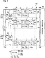
- FIG. 2 is a diagram showing the configuration of the power conversion device 100.
- the power conversion device 100 has first DC terminals 100A and second DC terminals 100B each pair of which is composed of both positive and negative terminals, and includes, between the first DC terminals 100A and the second DC terminals 100B, a plurality (M number) of DC/DC converters 10 (10a to 10h), and auxiliary converters 20 (20a to 20g) as balancing circuits.
- Each auxiliary converter 20 is connected between two DC/DC converters 10.
- the auxiliary converters 20 each connected between adjacent two DC/DC converters 10 are used as the balancing circuits, but without limitation thereto, anything that is connected between two DC/DC converters 10 and balances powers of the two DC/DC converters 10 may be used.
- the power conversion device 100 includes a controller for performing output control of the DC/DC converters 10 and the auxiliary converters 20 of the main circuit (power conversion unit).
- the controller includes: a first control unit 110 for controlling the entire main circuit; second control units 120 (120a to 120h) for controlling the respective DC/DC converters 10; and third control units 130 (130a to 130g) for controlling the respective auxiliary converters 20.
- Input voltage Vin of the power conversion device 100 is controlled to be target voltage Vin*, e.g., 25 kV, by the power conversion device 100.
- Output voltage Vout of the power conversion device 100 is controlled to be predetermined voltage, e.g., 350 kV, by the DC/AC conversion unit 310 of the electrical substation 300.
- DC power from the wind power generation system 200 is input to the first DC terminals 100A. That is, the first DC terminals 100A serve as the input terminals of the main circuit (power conversion unit) of the power conversion device 100, and the input voltage Vin is voltage of the first DC terminals 100A.
- the second DC terminals 100B serve as the output terminals of the main circuit of the power conversion device 100, and the output voltage Vout is voltage of the second DC terminals 100B.
- Output power from the power conversion device 100 is output to the electrical substation 300 via the DC power transmission cable 400 (not shown).
- Each DC/DC converter 10 includes: DC terminals 5A (hereinafter, first-side terminals 5A) on the primary side as the first side; DC terminals 5B (hereinafter, second-side terminals 5B) on the secondary side as the second side; a DC/AC conversion unit 2 on the primary side; a DC/AC conversion unit 3 on the secondary side; and a single-phase transformer 4 as a transformer. It is noted that, if insulation is not needed, only inductance LS may be connected instead of the single-phase transformer 4.
- the second control units 120 are provided for the respective DC/DC converters 10.
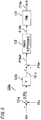
- FIG. 3 shows an example of a circuit diagram of the DC/DC converter 10a. It is noted that there are various types of converters as the DC/DC converters 10, and an appropriate type is selected in accordance with, for example, rated voltage, conversion capacity, operation frequency, and the like. The other DC/DC converters 10b to 10h are the same as the DC/DC converter 10a.
- the DC/AC conversion unit 2 on the primary side includes: a DC capacitor 6 connected between both poles of the first-side terminals 5A; and a first full-bridge circuit formed by two switching legs composed of semiconductor switching elements Q11 to Q14 as positive-side and negative-side semiconductor elements connected in series.
- the DC/AC conversion unit 3 on the secondary side includes: a DC capacitor 7 connected between both poles of the second-side terminals 5B; and a second full-bridge circuit formed by two switching legs composed of semiconductor switching elements Q21 to Q24 as positive-side and negative-side semiconductor elements connected in series.
- the single-phase transformer 4 is connected between intermediate connection points of the switching legs of the DC/AC conversion unit 2 and intermediate connection points of the switching legs of the DC/AC conversion unit 3.
- semiconductor switching elements Q11 to Q24 for example, semiconductor switching elements having a self-turn-off function, such as IGBTs (Insulated Gate Bipolar Transistors), to which diodes are connected in antiparallel, are used.
- IGBTs Insulated Gate Bipolar Transistors
- Each semiconductor switching element Q11 to Q24 may be used with a plurality of semiconductor switching elements combined in parallel, depending on the current capacity.
- a snubber capacitor CS is connected in parallel to each semiconductor switching element Q11 to Q24. Owing to effects of the snubber capacitor CS and the inductance LS of the AC output line, zero voltage switching which is soft switching of each semiconductor switching element Q11 to Q24 becomes possible.
- the second control unit 120a generates gate signals GlOa for the semiconductor switching elements Q11 to Q24 in the DC/DC converter 10a, thereby controlling switching of the semiconductor switching elements Q11 to Q24.
- the semiconductor switching elements Q11 to Q24 by soft switching of the semiconductor switching elements Q11 to Q24, switching loss can be reduced, the operation frequency can be increased, and the size of the single-phase transformer 4 can be reduced. It is noted that soft switching is technology in which, using a resonance phenomenon, voltage or current applied to a semiconductor switching element during a switching transient period is reduced to reduce switching loss and electromagnetic noise. As the inductance LS, the leakage inductance of the single-phase transformer 4 may be used.
- the DC/DC converter 10a is a circuit that converts DC voltage V1a applied to the first-side terminals 5A, to DC voltage V2a applied to the second-side terminals 5B, via the DC/AC conversion unit 2, the single-phase transformer 4, and the DC/AC conversion unit 3, and can be freely controlled so as to perform bidirectional power conversion. It is desirable that the turns ratio of the single-phase transformer 4 is matched with the ratio of the DC voltage V1a on the primary side and the DC voltage V2a on the secondary side. It is noted that the DC/DC converter 10a, in normal operation, steps up the primary-side voltage V1a on the input voltage Vin side and outputs the secondary-side voltage V2a to the output voltage Vout side.
- the first-side terminals 5A of the M number of DC/DC converters 10a to 10h are connected so that common current flows between both positive and negative terminals of the first DC terminals 100A of the power conversion device 100, and the second-side terminals 5B of the DC/DC converters 10a to 10h are connected so that common current flows between both positive and negative terminals of the second DC terminals 100B of the power conversion device 100.
- the positive terminal of the first-side terminals 5A of the DC/DC converter 10a is connected to the positive terminal of the first DC terminals 100A
- the negative terminal of the first-side terminals 5A of the DC/DC converter 10a is connected to the positive terminal of the first-side terminals 5A of the DC/DC converter 10b
- the negative terminals of the first-side terminals 5A of the DC/DC converters 10b to 10g are respectively connected to the positive terminals of the first-side terminals 5A of the DC/DC converters 10c to 10h.
- the negative terminal of the first-side terminals 5A of the DC/DC converter 10h is connected to the negative terminal of the first DC terminals 100A.
- the positive terminal of the second-side terminals 5B of the DC/DC converter 10a is connected to the positive terminal of the second DC terminals 100B
- the negative terminal of the second-side terminals 5B of the DC/DC converter 10a is connected to the positive terminal of the second-side terminals 5B of the DC/DC converter 10b
- the negative terminals of the second-side terminals 5B of the DC/DC converters 10b to 10g are respectively connected to the positive terminals of the second-side terminals 5B of the DC/DC converters 10c to 10h.
- the negative terminal of the second-side terminals 5B of the DC/DC converter 10h is connected to the negative terminal of the second DC terminals 100B.
- Each auxiliary converter 20 performs conversion between DC powers having different voltages, and in this case, is connected between two pairs of first-side terminals 5A of adjacent two DC/DC converters 10, to receive and pass power between the two pairs of first-side terminals 5A.
- the auxiliary converter 20a is connected between the first-side terminals 5A of the DC/DC converter 10a and the first-side terminals 5A of the DC/DC converter 10b.
- each auxiliary converter 20 may be connected between the first-side terminals 5A of two DC/DC converters 10.
- the M number of DC/DC converters 10c to 10h can be balanced via the M-1 number of auxiliary converters 20.
- Each auxiliary converter 20 has P terminals 25A connected to the first-side terminals 5A of the DC/DC converter 10 on the high-potential side, and N terminals 25B connected to the first-side terminals 5A of the DC/DC converter 10 on the low-potential side.
- the circuit configuration of each auxiliary converter 20 is the same as that of the DC/DC converter 10a, and has the same DC/AC conversion units 2, 3 and single-phase transformer 4 as those shown in FIG. 3 .
- the third control units 130 are provided for the respective auxiliary converters 20.
- the third control unit 130a that controls the auxiliary converter 20a generates gate signals G20a for the semiconductor switching elements Q11 to Q24 in the auxiliary converter 20a, thereby controlling switching of each semiconductor switching element Q11 to Q24.
- the first DC terminals 100A and the second DC terminals 100B of the power conversion device 100, the first-side terminals 5A and the second-side terminals 5B of each DC/DC converter 10, and the P terminals 25A and the N terminals 25B of each auxiliary converter 20 are all composed of two positive and negative terminals.
- voltage between the positive and negative terminals is referred to as voltage of the terminals.
- voltage of the P terminals 25A refers to voltage between the positive and negative terminals of the P terminals 25A.
- the first-side terminals 5A of the M number of DC/DC converters 10a to 10h are connected so that common current flows between both positive and negative terminals of the first DC terminals 100A of the power conversion device 100, and the second-side terminals 5B of the DC/DC converters 10a to 10h are connected so that common current flows between both positive and negative terminals of the second DC terminals 100B of the power conversion device 100.
- input voltage Vin which is voltage of the first DC terminals 100A is the sum of voltages V1 (V1a to V1h) of the first-side terminals 5A of the DC/DC converters 10 (10a to 10h).
- output voltage Vout which is voltage of the second DC terminals 100B is the sum of voltages V2 (V2a to V2h) of the second-side terminals 5B of the DC/DC converters 10 (10a to 10h).
- Vin V 1 a + V 1 b + ... + V 1 h
- Vout V 2 a + V 2 b + ... + V 2 h
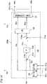
- FIG. 4 is a block diagram showing the entire configuration of the controller of the power conversion device 100, i.e., the entire configuration including the first control unit 110 for controlling the entire main circuit, the second control units 120 (120a to 120h) for controlling the respective DC/DC converters 10, and the third control units 130 (130a to 130g) for controlling the respective auxiliary converters 20.
- each second control unit 120 (120a to 120h) has means for detecting input and output voltages V1 (V1a to V1h), V2 (V2a to V2h), and the detected input and output voltages V1, V2 are transmitted to the first control unit 110.
- the first control unit 110 transmits voltage V1 of the P terminals 25A and voltage V1 of the N terminals 25B of each auxiliary converter 20 to the respective third control units 130 (130a to 130g).
- the first control unit 110 includes a Vin calculation unit 111, a Vout calculation unit 112, a Vin control unit 113, and an average value calculation unit 114.
- the Vin calculation unit 111 calculates input voltage Vin, using the above Expression (1)
- the Vout calculation unit 112 calculates output voltage Vout, using the above Expression (2).
- the Vin control unit 113 receives given target voltage Vin* and the input voltage Vin, and generates a power command P* as a first command so that the input voltage Vin is controlled to be the target voltage Vin*, that is, the input voltage Vin approaches the target voltage Vin*.
- the average value calculation unit 114 receives the output voltage Vout and the power command P*, and divides them by the number M of the DC/DC converters 10a to 10h.
- the first control unit 110 transmits the command voltage V2* and the power command value P10* to the second control unit 120 of each DC/DC converter 10.
- Each second control unit 120 (120a to 120h) detects the input and output voltages V1 (V1a to V1h), V2 (V2a to V2h) and transmits them to the first control unit 110, and generates the gate signal G10 (G10a to G10h) for controlling each DC/DC converter 10, on the basis of the command voltage V2* and the power command value P10*.
- FIG. 5 shows an example of a control block diagram illustrating the second control unit 120a for controlling the DC/DC converter 10a. It is noted that the second control units 120b to 120h are the same as the second control unit 120a.
- a subtractor 121a calculates a deviation ⁇ V2a between the command voltage V2* and the voltage V2a.
- a controller 121b calculates a first control command value 121c by, for example, proportional control so that the deviation ⁇ V2a approaches 0.
- the power command value P10* from the first control unit 110 is added to the first control command value 121c, whereby a control command P10a* for performing output control of the DC/DC converter 10a is generated.
- a phase difference generator 122 outputs a difference ⁇ 10a between switching phases of the DC/AC conversion unit 2 and the DC/AC conversion unit 3 in the DC/DC converter 10a, on the basis of the control command P10a*. It is noted that output power is controlled by delaying the switching phase of the semiconductor switching elements Q21 to Q24 in the DC/AC conversion unit 3 on the secondary side by a predetermined phase difference ⁇ [rad] relative to the switching phase of the semiconductor switching elements Q11 to Q14 in the DC/AC conversion unit 2 on the primary side.
- APWM signal generator 123 generates and outputs the gate signal GlOa which is a PWM signal for performing switching control of each semiconductor switching element Q11 to Q24 in the DC/DC converter 10a, on the basis of the phase difference ⁇ 810a.
- each third control unit 130 (130a to 130g) generates the gate signal G20 (G20a to G20g) for controlling each auxiliary converter 20, on the basis of voltage V1 of the P terminals 25A and voltage V1 of the N terminals 25B of each auxiliary converter 20.
- the third control unit 130a generates the gate signal G20a for controlling the auxiliary converter 20a, on the basis of voltage V1a of the P terminals 25A and voltage V1b of the N terminals 25B of the auxiliary converter 20a.
- FIG. 6 shows an example of a control block diagram illustrating the third control unit 130a for controlling the auxiliary converter 20a. It is noted that the third control units 130b to 130g are the same as the third control unit 130a.
- a subtractor 131a calculates a voltage difference ⁇ V1ab between voltage V1a of the P terminals 25A and voltage V1b of the N terminals 25B.
- a V1 controller 131b generates a power command (control command) 131c for performing output control of the auxiliary converter 20a, by, for example, proportional integral control so that the half of voltage difference ⁇ V1ab is compensated and voltage difference ⁇ V1ab approaches 0.
- a power transmission direction from the P terminals 25A to the N terminals 25B is defined as positive.
- V1a a positive power command 131c is generated so that the voltage V1a of the P terminals 25A approaches (V1a - ( ⁇ V1ab/2)).
- DC power is transmitted from the P terminals 25A to the N terminals 25B, voltage V1a of the P terminals 25A gradually decreases, and voltage V1b of the N terminals 25B gradually increases, so that the voltage difference ⁇ V1ab between voltage V1a and voltage V1b decreases.
- V1a ⁇ V1b a negative power command 131c is generated so that voltage V1b of the N terminals 25B approaches (V1b - ( ⁇ V1ab/2)).
- DC power is transmitted from the N terminals 25B to the P terminals 25A, voltage V1b of the N terminals 25B gradually decreases, and voltage V1a of the P terminals 25A gradually increases, so that the voltage difference ⁇ V1ab between voltage V1a and voltage V1b decreases.
- a phase difference generator 132 outputs a difference ⁇ 20a between switching phases of the DC/AC conversion unit 2 and the DC/AC conversion unit 3 in the auxiliary converter 20a, on the basis of the power command 131c.
- a PWM signal generator 133 generates and outputs the gate signal G20a which is a PWM signal for performing switching control of each semiconductor switching element Q11 to Q24 in the auxiliary converter 20a, on the basis of the phase difference ⁇ 20a.
- each auxiliary converter 20 is subjected to output control such that, on the basis of comparison between voltage V1 of the P terminals 25A and voltage V1 of the N terminals 25B, power is received and passed from the high-voltage side to the low-voltage side so as to equalize the two DC voltages.
- the third control unit 130a generates command voltage so that voltage of the terminals on the high-voltage side decreases by half the difference voltage, thereby controlling the corresponding auxiliary converter 20.
- each auxiliary converter 20 The P terminals 25A and the N terminals 25B of each auxiliary converter 20 are connected to the respective first-side terminals 5A of the two DC/DC converters 10, and two voltages of the first-side terminals 5A are controlled to be equalized by the auxiliary converter 20.
- voltages V1 (V1a to V1h) of the first-side terminals 5A of the M number of DC/DC converters 10 are controlled to be equalized.
- the M number of DC/DC converters 10 and the M-1 number of auxiliary converters 20 are controlled by the first control unit 110, the second control units 120, and the third control units 130.
- the second control unit 120 performs output control of the DC/DC converter 10 on the basis of the command voltage V2* for voltage V2 and the power command value P10*.
- the power command value P10* is calculated by dividing the power command P* for controlling the input voltage Vin of the entire power conversion device 100 to be the target voltage Vin*, by the number M of the DC/DC converters 10. Therefore, the DC/DC converters 10 operate so that each voltage V2 is controlled to be the command voltage V2* and the input voltage Vin of the entire power conversion device 100 is controlled to be the target voltage Vin*.
- Each second control unit 120 causes the DC/DC converter 10 to operate so that the voltage V2 is controlled to be the command voltage V2*, and when the voltage V2 is determined, the voltage V1 is automatically determined in accordance with the power to be transmitted.
- the DC/DC converters 10 have the same configuration, and each voltage V1 determined by operation thereof becomes, ideally, a value (Vin*/M) obtained by dividing the target voltage Vin* for input voltage Vin by the number M of the DC/DC converters 10.
- Vin*/M a value obtained by dividing the target voltage Vin* for input voltage Vin by the number M of the DC/DC converters 10.
- error occurs by factors such as variation in components and detection error of detectors. Therefore, although the input voltage Vin which is the sum of voltages V1 can be controlled to be the target voltage Vin*, variation occurs among the voltages V1.
- the target voltages for input voltage Vin and output voltage Vout of the power conversion device 100 are set as the power transmission system 1, the target voltages are controlled to be constant. Therefore, the step-up ratio (Vout/Vin) of the power conversion device 100 also becomes a constant value, and the input and output voltages V1, V2 of each DC/DC converter 10 becomes approximately constant values.
- voltages of generated powers sent from the plurality of electric generators 210a, 201b via the power conditioners 220a, 220b are stepped up by the respective step-up DC/DC conversion units 230a, 230b and the resultant powers are collected together to be input to the power conversion device 100.
- the power conversion device 100 further steps up voltage of the input DC power and transmits the resultant power to the electrical substation 300.
- the power conversion device 100 has a plurality of DC/DC converters 10 of which the input terminals (first-side terminals 5A) are connected so that common current flows between both positive and negative terminals of the input terminals (first DC terminals 100A) of the power conversion device 100 and the output terminals (second-side terminals 5B) are connected so that common current flows between both positive and negative terminals of the output terminals (second DC terminals 100B) of the power conversion device 100. Therefore, voltage assignment per one DC/DC converter 10 can be reduced. This enables application to high-voltage usage in which the input voltage Vin is equal to or higher than the withstand voltages of elements such as the semiconductor switching elements in the power conversion device 100. Each DC/DC converter 10, normally, further steps up the input voltage and outputs the resultant voltage, thus enabling output of DC power having further high voltage.
- the power conversion device 100 further steps up voltage of the input high-voltage DC power and transmits the resultant power, whereby the power transmission system 1 enables power transmission with high efficiency and over a long distance.
- the input voltage Vin of the power conversion device 100 needs to be controlled to be constant by the power conversion device 100.
- the auxiliary converters 20 are each provided between two DC/DC converters 10, on the input side.
- the DC/DC converters 10 operate so that each voltage V2 on the output voltage Vout side is controlled to be the command voltage V2*, the input voltage Vin is controlled to be the target voltage Vin*, and each voltage V1 on the input voltage Vin side is automatically determined.
- the voltages V2 are controlled to be equalized, and the input voltage Vin is controlled to be the target voltage Vin*.
- variation among the voltages V1 in the input voltage Vin is eliminated and the voltages V1 are controlled to be equalized.
- the power conversion device 100 allows input of high-voltage DC power from a power source having varying voltage and can reliably perform output control, and the input voltages V1, the output voltages V2, and the power loads can be equalized among the DC/DC converters 10. Therefore, it becomes possible to reduce a margin provided in consideration of errors such as variation in components and detection errors of detectors, whereby size reduction and cost reduction of the power conversion device 100 can be achieved.
- Each auxiliary converter 20 only has to transmit power corresponding to half the difference voltage between input voltages of two DC/DC converters 10. Therefore, the power capacity of the auxiliary converters 20 can be made smaller than that of the DC/DC converters 10. That is, the element capacity of the semiconductor switching elements Q in each auxiliary converter 20 can be reduced. It is noted that power received and passed by each auxiliary converter 20 is only transferred between the DC/DC converters 10 and therefore does not influence power transmitted by the power conversion device 100.
- Each DC/DC converter 10 controls only one voltage V2 of the input and output voltages to be the command voltage V2*, and each auxiliary converter 20 controls only the high-voltage-side voltage which is one of the input and output voltages, to be the command voltage. Therefore, the DC/DC converters 10 and the auxiliary converters 20 can be realized with a simple configuration, whereby the size and the cost can be further reduced.
- auxiliary converters 20 are provided on the input voltage side of the power conversion device 100, lower voltage is used as compared to the case where the auxiliary converters 20 are provided on the output voltage side as described later. Therefore, the capacities of elements such as the semiconductor switching elements Q in each auxiliary converter 20 can be reduced, whereby size reduction and cost reduction can be achieved.
- means for detecting the input and output voltages V1, V2 of each DC/DC converter 10 is provided to each second control unit 120, but may be provided to the first control unit 110 or may be provided to both control units.
- the input voltage Vin and the output voltage Vout of the power conversion device 100 are calculated by the first control unit 110.
- the first control unit 110 may have means for detecting the input voltage Vin and the output voltage Vout.
- the controller has the first control unit 110, the second control units 120, and the third control units 130, and performs output control of the DC/DC converters 10 and the auxiliary converters 20, but the configuration is not limited thereto.
- the controller is configured without the third control unit 130, and thus only the DC/DC converters 10 are control targets.
- the auxiliary converters 20 are provided on the input voltage side of the power conversion device 100, whereas in the present embodiment, the auxiliary converters 20 are provided on the output voltage side.
- the configuration of the power transmission system 1 is the same as that described in FIG. 1 in the above Embodiment 1.
- FIG. 7 is a diagram showing the configuration of a power conversion device 101 according to the present Embodiment 2.
- the power conversion device 101 has first DC terminals 101B and second DC terminals 101A each pair of which is composed of both positive and negative terminals.
- DC power from the wind power generation system 200 is input to the second DC terminals 101A. That is, the second DC terminals 101A serve as the input terminals of the main circuit (power conversion unit) of the power conversion device 101, and the input voltage Vin is voltage of the second DC terminals 101A.
- the first DC terminals 101B serve as the output terminals of the main circuit of the power conversion device 101, and the output voltage Vout is voltage of the first DC terminals 101B.
- the power conversion device 101 includes, between the input terminals (second DC terminals 101A) and the output terminals (first DC terminals 101B), a plurality (M number) of DC/DC converters 10 (10a to 10h) and M-1 number of auxiliary converters 20 (20a to 20g).
- the power conversion device 101 includes a controller for performing output control of the DC/DC converters 10 and the auxiliary converters 20 of the main circuit.
- the controller includes: a first control unit 110a for controlling the entire main circuit; second control units 120 (120a to 120h) for controlling the respective DC/DC converters 10; and third control units 130 (130a to 130g) for controlling the respective auxiliary converters 20.
- Each DC/DC converter 10 includes: DC terminals 5A (first-side terminals 5A) on the secondary side as the first side; DC terminals 5B (second-side terminals 5B) on the primary side as the second side; a DC/AC conversion unit 2 on the first side; a DC/AC conversion unit 3 on the second side; and a single-phase transformer 4.
- the circuit configuration of each DC/DC converter 10 is the same as that shown in FIG. 3 in the above Embodiment 1, but in the present Embodiment 2, the input/output relationship between the first-side terminals 5A and the second-side terminals 5B is reversed. It is noted that the circuit of each DC/DC converter 10 is right-left symmetric and thus is capable of bidirectional operations, and therefore, merely the first side and the second side as the terms for input and output sides are reversed.
- the second control units 120 are provided for the respective DC/DC converters 10.
- the first-side terminals 5A of the M number of DC/DC converters 10a to 10h are connected so that common current flows between both positive and negative terminals of the first DC terminals 101B of the power conversion device 101, and the second-side terminals 5B of the DC/DC converters 10a to 10h are connected so that common current flows between both positive and negative terminals of the second DC terminals 101A of the power conversion device 101.
- Each auxiliary converter 20 performs conversion between DC powers having different voltages, and is connected between two pairs of first-side terminals 5A of two DC/DC converters 10, to receive and pass power between the two pairs of first-side terminals 5A.
- Each auxiliary converter 20 has P terminals 25A connected to the first-side terminals 5A of the DC/DC converter 10 on the high-potential side, and N terminals 25B connected to the first-side terminals 5A of the DC/DC converter 10 on the low-potential side.
- the circuit configuration of each auxiliary converter 20 is the same as that of the DC/DC converter 10a, and has the same DC/AC conversion units 2, 3 and single-phase transformer 4 as those shown in FIG. 3 .
- the third control units 130 are provided for the respective auxiliary converters 20.
- the first-side terminals 5A of the M number of DC/DC converters 10a to 10h are connected so that common current flows between both positive and negative terminals of the first DC terminals 101B of the power conversion device 101, and the second-side terminals 5B thereof are connected so that common current flows between both positive and negative terminals of the second DC terminals 101A of the power conversion device 101.
- input voltage Vin which is voltage of the second DC terminals 101A is the sum of voltages V2 (V2a to V2h) of the second-side terminals 5B of the DC/DC converters 10 (10a to 10h).
- output voltage Vout which is voltage of the first DC terminals 101B is the sum of voltages V1 (V1a to V1h) of the first-side terminals 5A of the DC/DC converters 10 (10a to 10h).
- Vin V 2 a + V 2 b + ... + V 2 h
- Vout V 1 a + V 1 b + ... + V 1 h
- FIG. 8 is a block diagram showing the entire configuration of the controller of the power conversion device 101, i.e., the entire configuration including the first control unit 110a for controlling the entire main circuit, the second control units 120 (120a to 120h) for controlling the respective DC/DC converters 10, and the third control units 130 (130a to 130g) for controlling the respective auxiliary converters 20.
- each second control unit 120 (120a to 120h) has means for detecting input and output voltages V2 (V2a to V2h), V1 (V1a to V1h), and the detected input and output voltages V2, V1 are transmitted to the first control unit 110a.
- the first control unit 110a transmits voltage V1 of the P terminals 25A and voltage V1 of the N terminals 25B of each auxiliary converter 20 to the respective third control units 130 (130a to 130g).
- the first control unit 110a includes a Vin calculation unit 111a, a V1 distribution unit 112a, a Vin control unit 113, and an average value calculation unit 114.
- the V1 distribution unit 112a transmits voltages V1 of the P terminals 25A and the N terminals 25B of the auxiliary converters 20 to the respective third control units 130.
- the Vin calculation unit 111a calculates input voltage Vin, using the above Expression (3).
- the Vin control unit 113 receives given target voltage Vin* and the input voltage Vin, and generates a power command P* as a first command so that the input voltage Vin is controlled to be the target voltage Vin*, that is, the input voltage Vin approaches the target voltage Vin*.
- the first control unit 110a transmits the command voltage V2* and the power command value P10* to the second control unit 120 of each DC/DC converter 10.
- Each second control unit 120 detects the input and output voltages V2 (V2a to V2h), V1 (V1a to V1h) and transmits them to the first control unit 110a, and generates the gate signal G10 (G10a to G10h) for controlling each DC/DC converter 10, on the basis of the command voltage V2* and the power command value P10*.
- the second control unit 120a that controls the DC/DC converter 10a will be described below.
- a subtractor 121a calculates a deviation ⁇ V2a between the command voltage V2* and the voltage V2a.
- a controller 121b calculates a first control command value 121c by, for example, proportional control so that the deviation ⁇ V2a approaches 0.
- the power command value P10* from the first control unit 110a is added to the first control command value 121c, whereby a control command P10a* for performing output control of the DC/DC converter 10a is generated.
- a phase difference generator 122 outputs a difference ⁇ 10a between switching phases of the DC/AC conversion unit 2 and the DC/AC conversion unit 3 in the DC/DC converter 10a, on the basis of the control command P10a*. Then, a PWM signal generator 123 generates and outputs the gate signal GlOa which is a PWM signal for performing switching control of each semiconductor switching element Q11 to Q24 in the DC/DC converter 10a, on the basis of the phase difference ⁇ 10a.
- Each third control unit 130 (130a to 130g) generates the gate signal G20 (G20a to G20g) for controlling each auxiliary converter 20, on the basis of voltage V1 of the P terminals 25A and voltage V1 of the N terminals 25B of each auxiliary converter 20.
- the third control unit 130a generates the gate signal G20a for controlling the auxiliary converter 20a, on the basis of voltage V1a of the P terminals 25A and voltage V1b of the N terminals 25B of the auxiliary converter 20a.
- the third control unit 130 is the same as in the above Embodiment 1, and each auxiliary converter 20 is subjected to output control such that, on the basis of comparison between voltage V1 of the P terminals 25A and voltage V1 of the N terminals 25B, power is received and passed from the high-voltage side to the low-voltage side so as to equalize the two DC voltages.
- voltage V2 controlled by each DC/DC converter 10 is output voltage, whereas in the present Embodiment 2, voltage V2 is input voltage.
- each voltage V2 and the input voltage Vin of the power conversion device 101 can be controlled in the same manner as in the above Embodiment 1.
- the second control unit 120 performs output control of the DC/DC converter 10 on the basis of the command voltage V2* for voltage V2 and the power command value P10*.
- the power command value P10* is calculated by dividing the power command P* for controlling the input voltage Vin of the entire power conversion device 101 to be the target voltage Vin*, by the number M of the DC/DC converters 10. Therefore, the DC/DC converters 10 operate so that each voltage V2 is controlled to be the command voltage V2* and the input voltage Vin of the entire power conversion device 101 is controlled to be the target voltage Vin*.
- Each second control unit 120 causes the DC/DC converter 10 to operate so that the voltage V2 is controlled to be the command voltage V2*, and when the voltage V2 is determined, the voltage V1 is automatically determined in accordance with the power to be transmitted.
- the DC/DC converters 10 have the same configuration, and the voltage V1 determined by operation thereof becomes, ideally, a value (Vout/M) obtained by dividing the output voltage Vout by the number M of the DC/DC converters 10.
- Vout/M a value obtained by dividing the output voltage Vout by the number M of the DC/DC converters 10.
- error occurs by factors such as variation in components and detection error of detectors. Therefore, variation occurs among the voltages V1.
- the power conversion device 101 is configured with a plurality of DC/DC converters 10 connected, voltage assignment per one DC/DC converter 10 can be reduced, and the input voltage Vin can be increased to be high voltage.
- the auxiliary converters 20 are each provided between two DC/DC converters 10, on the output side, thus enabling control of both input and output voltages of each DC/DC converter 10. Therefore, as in the above Embodiment 1, the power conversion device 101 allows input of high-voltage DC power from a power source having varying voltage and can reliably perform output control, and the input voltages V1, the output voltages V2, and the power loads can be equalized among the DC/DC converters 10. Therefore, it becomes possible to reduce a margin provided in consideration of errors such as variation in components and detection errors of detectors, whereby size reduction and cost reduction of the power conversion device 101 can be achieved.
- Each auxiliary converter 20 only has to transmit power corresponding to half the difference voltage between input voltages of two DC/DC converters 10. Therefore, the power capacity of the auxiliary converters 20 can be made smaller than that of the DC/DC converters 10.
- Each DC/DC converter 10 controls only one voltage V2 of the input and output voltages to be the command voltage V2*, and each auxiliary converter 20 controls only the high-voltage-side voltage which is one of the input and output voltages, to be the command voltage. Therefore, the DC/DC converters 10 and the auxiliary converters 20 can be realized with a simple configuration, whereby the size and the cost can be further reduced.
- each DC/DC converter 10 shown in the above Embodiment 1 is configured by connecting a plurality (N number) of converter cells 30 (30a to 30x).
- the controller of the power conversion device 100 includes: a first control unit 110 for controlling the entire main circuit; second control units 120 (120a to 120h) for controlling the respective DC/DC converters 10; and third control units 130 (130a to 130g) for controlling the respective auxiliary converters 20.
- Each second control unit 120 includes a control unit for the DC/DC converter 10 and cell control units 140 for controlling the respective converter cells 30.
- the configurations other than the DC/DC converter 10 and the second control unit 120 are the same as in the above Embodiment 1.
- FIG. 9 shows an example of a circuit diagram of the DC/DC converter 10a according to the present Embodiment 3. It is noted that the other DC/DC converters 10b to 10h are the same as the DC/DC converter 10a. As shown in FIG. 9 , the DC/DC converter 10a includes a plurality of converter cells 30 (30a to 30x) between the first-side terminals 5A and the second-side terminals 5B.
- FIG. 10 shows an example of a circuit diagram of the converter cell 30a
- FIG. 11 shows the second control unit 120a for controlling the DC/DC converter 10a.
- the second control unit 120a for controlling the DC/DC converter 10a is composed of a control unit 120aa for controlling the entire circuit of the DC/DC converter 10a, and the cell control units 140 (140a to 140x) for controlling the respective converter cells 30 (30a to 30x).
- Each converter cell 30 includes, between primary-side DC terminals 15A as A terminals and secondary-side DC terminals 15B as B terminals, a DC/AC conversion unit 12 on the primary side, a DC/AC conversion unit 13 on the secondary side, and a single-phase transformer 14.
- the cell control units 140 are provided for the respective converter cells 30.
- the DC terminals 15A on the primary side are connected in parallel to the first-side terminals 5A of the DC/DC converter 10a, and the DC terminals 15B on the secondary side are connected so that common current flows between both poles of the second-side terminals 5B of the DC/DC converter 10a. That is, the input sides of the plurality of converter cells 30 composing the DC/DC converter 10a are connected in parallel and the output sides thereof are connected so that common current flows.
- the converter cell 30a is configured as shown in FIG. 10 . It is noted that there are various types of converter cells as the converter cells 30, and an appropriate type is selected in accordance with, for example, rated voltage, conversion capacity, operation frequency, and the like.
- the other converter cells 30b to 30x are the same as the converter cell 30a. It is noted that, in this case, the circuit configuration of the converter cell 30a is the same as that of the DC/DC converter 10a shown in FIG. 3 in the above Embodiment 1.
- the DC/AC conversion unit 12 on the primary side includes: a DC capacitor 6a connected between both poles of the DC terminals 15A; and a first full-bridge circuit formed by two switching legs composed of semiconductor switching elements Q11a to Q14a as positive-side and negative-side semiconductor elements connected in series.
- the DC/AC conversion unit 13 on the secondary side includes: a DC capacitor 7a connected between both poles of the DC terminals 15B; and a second full-bridge circuit formed by two switching legs composed of semiconductor switching elements Q21a to Q24a as positive-side and negative-side semiconductor elements connected in series.
- the single-phase transformer 14 as a transformer is connected between intermediate connection points of the switching legs of the DC/AC conversion unit 12 and intermediate connection points of the switching legs of the DC/AC conversion unit 13. It is noted that, if insulation is not needed, only inductance LS may be connected instead of the single-phase transformer 14.
- semiconductor switching elements Q11a to Q24a for example, semiconductor switching elements having a self-turn-off function, such as IGBTs, to which diodes are connected in antiparallel are used.
- semiconductor switching element Q11a to Q24a may be used with a plurality of semiconductor switching elements combined in parallel, depending on the current capacity.
- a snubber capacitor CS is connected in parallel to each semiconductor switching element Q11a to Q24a. Owing to effects of the snubber capacitor CS and the inductance LS of the AC output line, zero voltage switching which is soft switching of each semiconductor switching element Q11a to Q24a becomes possible.
- the cell control unit 140a generates gate signals G30a for the semiconductor switching elements Q11a to Q24a in the converter cell 30a, thereby controlling switching of the semiconductor switching elements Q11a to Q24a.
- the converter cell 30a since the DC terminals 15A are connected in parallel to the first-side terminals 5A of the DC/DC converter 10a, the DC voltage V1a applied to the first-side terminals 5A is applied to the DC terminals 15A. Further, the converter cell 30a is a circuit that converts the DC voltage V1a to DC voltage V21a applied to the DC terminals 15B, via the DC/AC conversion unit 12, the single-phase transformer 14, and the DC/AC conversion unit 13, and can be freely controlled so as to perform bidirectional power conversion. It is desirable that the turns ratio of the single-phase transformer 14 is matched with the ratio of the DC voltage V1a on the primary side and the DC voltage V21a on the secondary side.
- DC/DC converter 10a composed of the plurality of converter cells 30, in normal operation, steps up the primary-side voltage V1a and outputs the secondary-side voltage V21a, but the operation of each converter cell 30 is not limited to step-up operation.
- the DC capacitors 6a, 7a electrolytic capacitors, film capacitors, or the like are used. High-frequency current flows through the DC capacitors 6a, 7a, but in the case of using film capacitors, deterioration due to the high-frequency current can be suppressed and thus the life of the capacitors is prolonged.
- the DC terminals 15B of the N number of converter cells 30a to 30x in the DC/DC converter 10a are connected so that common current flows between both positive and negative terminals of the second-side terminals 5B of the DC/DC converter 10a.
- voltage V2a of the second-side terminals 5B of the DC/DC converter 10a is the sum of voltages V21 (V21a to V21x) of the DC terminals 15B on the output side of the converter cells 30 (30a to 30x).
- voltage V2a of the second-side terminals 5B which is output voltage of the DC/DC converter 10a is represented by Expression (5).
- V 2 a V 21 a + V 21 b + ... + V 21 x
- the control unit 120aa detects input and output voltages V1a, V2a of the DC/DC converter 10a, and transmits them to the first control unit 110 (not shown). It is noted that the detection of voltage V2a is performed through calculation as described later.
- Each cell control unit 140 has means for detecting voltage V21 (V21a to V21x) of the DC terminals 15B which is output voltage of each converter cell 30, and transmits the detected voltage V21 to the control unit 120aa.
- the received command voltage V2* and power command value P10* are input to the control unit 120aa.
- the control unit 120aa includes a V2 control unit 121, a V2 calculation unit 125, and an average value calculation unit 126.
- the V2 calculation unit 125 calculates voltage V2a using the above Expression (5) on the basis of the voltages V21 received from the cell control units 140.
- the V2 control unit 121 receives the command voltage V2* from the first control unit 110 and the voltage V2a, and calculates a first control command value 121c so that the voltage V2a approaches the command voltage V2*.
- the power command value P10* from the first control unit 110 is added to the first control command value 121c, whereby a control command P10a* for performing output control of the DC/DC converter 10a is generated.
- the average value calculation unit 126 receives the voltage V2a and the control command P10a* and divides them by the number N of the converter cells 30a to 30x.
- the control unit 120aa transmits the command voltage V21* and the power command value P30* to the cell control unit 140 of each converter cell 30.
- Each cell control unit 140 (140a to 140x) generates the gate signal G30 (G30a to G30x) for controlling each converter cell 30, on the basis of the command voltage V21* and the power command value P30*.
- FIG. 12 is a block diagram showing the entire configuration of the controller of the power conversion device 100, i.e., the entire configuration including the first control unit 110 for controlling the entire main circuit, the second control units 120 (120a to 120h) for controlling the respective DC/DC converters 10, and the third control units 130 (130a to 130g) for controlling the respective auxiliary converters 20.
- Each second control unit 120 includes the control unit 120aa for controlling the entire circuit of the corresponding DC/DC converter 10, and the cell control units 140 (140a to 140x) for controlling the N number of converter cells 30 in the DC/DC converter 10.
- FIG. 13 is a control block diagram showing the first control unit 110.
- FIG. 14 is a control block diagram showing the control unit 120aa for controlling the DC/DC converter 10a
- FIG. 15 is a control block diagram showing the cell control unit 140a for controlling the converter cell 30a in DC/DC converter 10a.
- FIG. 16 is a control block diagram showing the third control unit 130a for controlling the auxiliary converter 20a.
- FIG. 14 shows the details of the control unit 120aa shown in FIG. 11 .
- the first control unit 110 receives voltages V1 (V1a to V1h) and voltages V2 (V2a to V2h) of the DC/DC converters 10 from the control units 120aa of the DC/DC converters 10. Then, the first control unit 110 transmits the voltages V1 (V1a to V1h) to the respective third control units 130.
- the Vin calculation unit 111 calculates input voltage Vin, using the above Expression (1), and the Vout calculation unit 112 calculates output voltage Vout, using the above Expression (2).
- a subtractor 113a calculates a deviation ⁇ Vin between given target voltage Vin* and the input voltage Vin.
- a controller 113b generates a power command P* as a first command by proportional integral control so that the deviation ⁇ Vin approaches 0.
- the average value calculation unit 114 receives the output voltage Vout and the power command P*, and divides them by the number M of the DC/DC converters 10a to 10h.
- the generated command voltage V2* and power command value P10* are transmitted via a signal distributor 115 to the control units 120aa to 120ha in the respective second control units 120 (120a to 120h).
- control unit 120aa in the second control unit 120a for controlling the DC/DC converter 10a will be described. It is noted that the control units 120ba to 120ha of the other second control units 120b to 120h are the same as the control unit 120aa.
- the command voltage V2* from the first control unit 110 and the voltage V2a are input and the voltages V21 (V21a to V21x) of the converter cells 30 are received from the respective cell control units 140 (140a to 140x).
- the control unit 120aa transmits the input and output voltage V1a, V2a of the DC/DC converter 10a to the first control unit 110.
- the V2 calculation unit 125 calculates the voltage V2a using the above Expression (5) on the basis of the voltages V21 received from the respective cell control units 140.
- a subtractor 121a calculates a deviation ⁇ V2a between the command voltage V2* from the first control unit 110 and the voltage V2a.
- a controller 121b generates a first control command value 121c by proportional control so that the deviation ⁇ V2a approaches 0.
- the power command value P10* from the first control unit 110 is added to the first control command value 121c, whereby a control command P10a* for performing output control of the DC/DC converter 10a is generated.
- the average value calculation unit 126 receives the voltage V2a and the control command P10a* and divides them by the number N of the converter cells 30a to 30x.
- the generated command voltage V21* and power command value P30* are transmitted via a signal distributor 127 to the cell control units 140 (140a to 140x).
- the cell control unit 140a for controlling the converter cell 30a in the DC/DC converter 10a will be described. It is noted that the other cell control units 140b to 140x are the same as the cell control unit 140a.
- the cell control unit 140a receives the command voltage V21* and the power command value P30* from the control unit 120aa. In addition, the cell control unit 140a detects voltage V21a of the DC terminals 15B which is output voltage of the converter cell 30a, and transmits the detected voltage V21a to the control unit 120aa.
- a subtractor 141a calculates a deviation ⁇ V21a between the command voltage V21* from the control unit 120aa and the voltage V21a.
- a controller 141b calculates a third control command value 141c by proportional control so that the deviation ⁇ V21a approaches 0.
- the power command value P30* (second control command value) from the control unit 120aa is added to the third control command value 141c, whereby a control command P30a* for performing output control of the converter cell 30a is generated.
- a phase difference generator 142 outputs a difference ⁇ 30a between switching phases of the DC/AC conversion unit 12 and the DC/AC conversion unit 13 in the converter cell 30a, on the basis of the control command P30a*.
- a PWM signal generator 143 generates and outputs the gate signal G30a which is a PWM signal for performing switching control of each semiconductor switching element Q11a to Q24a in the converter cell 30a, on the basis of the phase difference ⁇ 30a.
- the control command P30a* for performing output control of the converter cell 30a is generated by adding the third control command value 141c and the power command value P30*, and the power command value P30* is generated by adding the first control command value 121c and the power command value P10*. That is, the control command P30a* for performing output control of the converter cell 30a is a power command for compensating variation in the input voltage Vin of the power conversion device 100, compensating variation in the output voltage V2a of the DC/DC converter 10a, and compensating variation in the output voltage V21a of the converter cell 30a.
- the third control unit 130a for controlling the auxiliary converter 20a will be described. It is noted that the other third control units 130b to 130g are the same as the third control unit 130a.
- the third control unit 130a receives the voltage V1a of the P terminals 25A and the voltage V1b of the N terminals 25B of the auxiliary converter 20a from the first control unit 110.
- the third control unit 130a operates in the same manner as in the above Embodiment 1. That is, in the third control unit 130a, a subtractor 131a calculates a voltage difference ⁇ V1ab between voltage V1a of the P terminals 25A and voltage V1b of the N terminals 25B. A V1 controller 131b generates a power command (control command) 131c for performing output control of the auxiliary converter 20a by proportional integral control so that the half of voltage difference ⁇ V1ab is compensated and voltage difference ⁇ V1ab approaches 0.
- control is performed such that, on the basis of comparison between voltage V1a of the P terminals 25A and voltage V1b of the N terminals 25B, command voltage is generated so as to decrease voltage of the high-voltage-side terminal by half the voltage difference ⁇ V1ab and thus power is received and passed from the high-voltage side to the low-voltage side so as to equalize the two DC voltages.
- a phase difference generator 132 outputs a difference ⁇ 20a between switching phases of the DC/AC conversion unit 2 and the DC/AC conversion unit 3 in the auxiliary converter 20a, on the basis of the power command 131c.
- a PWM signal generator 133 generates and outputs the gate signal G20a which is a PWM signal for performing switching control of each semiconductor switching element Q11 to Q24 in the auxiliary converter 20a, on the basis of the phase difference ⁇ 20a.
- powers transmitted by each converter cell 30 and each auxiliary converter 20 can be controlled by calculating the phase differences ⁇ [rad] between the switching phase of the DC/AC conversion unit 12, 2 on the primary side and the switching phase of the DC/AC conversion unit 13, 3 on the secondary side.
- transmitted power P can be controlled by generating the phase difference ⁇ for controlling output power, and performing switching such that the phase difference ⁇ [rad] is provided between the primary-side circuit and the secondary-side circuit.
- the power P transmitted from the primary-side DC terminals 15A to the secondary-side DC terminals 15B is represented by the following Expression (6).
- P V 1 a ⁇ V21a / ⁇ LS ⁇ ⁇ ⁇ ⁇ 2 / ⁇
- ⁇ is a value obtained by multiplying a switching frequency fsw by 2 ⁇ .
- the phase difference ⁇ for controlling the transmitted power can be calculated by the following Expression (8).
- ⁇ ⁇ / 2 ⁇ ⁇ ⁇ 2 / 4 ⁇ ⁇ P/Vdc 2 ⁇ ⁇ LS
- electrostatic energy W stored in the DC capacitor 7a is calculated by the following Expression (9).
- Cdc is the capacitance of the DC capacitor 7a.
- control of the output voltage V21a of the converter cell 30a can be performed by increasing or decreasing the transmitted power of the converter cell 30a by power Pa that compensates the variation amount ⁇ w of the electrostatic energy W.
- the power Pa that compensates the variation amount ⁇ w can be calculated by the following Expression (11).
- the power Pa calculated by the above Expression (11) is power that compensates slight voltage variation ⁇ V21a occurring in the DC voltage V21a applied to the DC capacitor 7a on the secondary side, and therefore the power Pa is smaller as compared to the transmitted power of the converter cell 30a. In this case, the corresponding phase difference ⁇ a also becomes small, and therefore the above Expression (7) can be approximated as shown by the following Expression (12).
- the power conversion device 100 has a plurality of DC/DC converters 10 connected to each other, and has auxiliary converters 20 each provided between two DC/DC converters 10, on the input side. Further, each DC/DC converter 10 is composed of a plurality of converter cells 30, the input sides of the plurality of converter cells 30 in each DC/DC converter 10 are connected in parallel, and the output sides thereof are connected so that common current flows. Therefore, the same effects as in the above Embodiment 1 are obtained, and in addition, the following effects are obtained.
- each DC/DC converter 10 can have a great step-up ratio.
- the output voltages of the converter cells 30 are equally controlled by the cell control units 140, so that power loads thereof can be equalized. Therefore, it becomes possible to reduce a margin provided in consideration of errors such as variation in components and detection errors of detectors, whereby size reduction and cost reduction of the converter cells 30 can be achieved.
- Each auxiliary converter 20 only has to transmit power corresponding to half the difference voltage between the input voltages of two DC/DC converters 10. Since the input voltage of each DC/DC converter 10 is the same as the input voltages of the converter cells 30 in the DC/DC converter 10, the power capacity of the auxiliary converter 20 can be made smaller than the power capacities of the converter cells 30.
- the first control unit 110 uses proportional integral control for calculation of the power command P* for controlling the input voltage Vin
- the third control unit 130 uses proportional integral control for calculation for output control of each auxiliary converter 20. Using the proportional integral control enables enhancement of accuracy of the voltage control.
- the input voltage Vin of the power conversion device 100 is voltage of the power transmission system 1, and therefore needs to be controlled with high accuracy.
- the Vin control unit 113 is configured with the proportional integral controller (controller 113b), high-accuracy control can be performed.
- proportional control is used for calculations of the first control command value 121c for output control of each DC/DC converter 10 and the third control command value 141c for output control of each converter cell 30.
- the output voltage V2 of the DC/DC converter 10 is controlled using the average value as the command voltage V2*.
- the first control command value 121c calculated using proportional control compensates only an amount corresponding to variation relative to the average value.
- the third control command value 141c calculated using proportional control compensates only an amount corresponding to variation relative to the average value of output voltage of each converter cell 30.
- output voltages of the converter cells 30 in the DC/DC converter 10a are detected by the respective cell control units 140 in the second control unit 120a. However, these output voltages may be detected by the control unit 120aa, or may be detected by the first control unit 110.
- the DC/DC converters 10 each composed of a plurality of converter cells 30 are applied to Embodiment 1.
- such DC/DC converters 10 may be applied to the above Embodiment 2. That is, each auxiliary converter 20 may be provided between two DC/DC converters 10, on the output side, and also in this case, the same effects can be obtained.
- the DC/DC converters 10, the auxiliary converters 20, and the converter cells 30 used in the above embodiments 1 to 3 have such a configuration that full-bridge circuits each formed by two switching legs are provided on both sides of a transformer.
- a configuration having three-phase bridge circuits may be employed.
- the converter cells shown in the above Embodiment 3 are configured such that three-phase bridge circuits each formed by three switching legs are provided on both sides of a transformer.
- the other configurations are the same as in the above Embodiment 3.
- each DC/DC converter 10 includes a plurality of converter cells 40 between the first-side terminals 5A and the second-side terminals 5B.
- the controller of the power conversion device 100 includes: a first control unit 110 for controlling the entire main circuit; second control units 120 for controlling the respective DC/DC converters 10; and third control units 130 for controlling the respective auxiliary converters 20.
- Each second control unit 120 includes a control unit for the DC/DC converter 10 and cell control units 140 for controlling the respective converter cells 40.
- FIG. 17 is a circuit diagram of each converter cell 40 according to the present Embodiment 4.
- Each converter cell 40 includes, between primary-side DC terminals 15A as A terminals and secondary-side DC terminals 15B as B terminals, a DC/AC conversion unit 22 on the primary side, a DC/AC conversion unit 23 on the secondary side, and a three-phase transformer 24 as a transformer.
- the cell control units 140 are provided for the respective converter cells 40.
- the DC terminals 15A on the primary side are connected in parallel to the first-side terminals 5A of the DC/DC converter 10, and the DC terminals 15B on the secondary side are connected so that common current flows between both poles of the second-side terminals 5B of the DC/DC converter 10. That is, the input sides of the plurality of converter cells 40 composing the DC/DC converter 10 are connected in parallel and the output sides thereof are connected so that common current flows.
- the DC/AC conversion unit 22 on the primary side includes: a DC capacitor 6a connected between both poles of the DC terminals 15A; and a first three-phase bridge circuit formed by three switching legs composed of semiconductor switching elements Q11a to Q16a as positive-side and negative-side semiconductor elements connected in series.
- the DC/AC conversion unit 23 on the secondary side includes: a DC capacitor 7a connected between both poles of the DC terminals 15B; and a second three-phase bridge circuit formed by three switching legs composed of semiconductor switching elements Q21a to Q26a as positive-side and negative-side semiconductor elements connected in series.
- the three-phase transformer 24 is connected between intermediate connection points of the switching legs of the DC/AC conversion unit 22 and intermediate connection points of the switching legs of the DC/AC conversion unit 23.
- semiconductor switching elements Q11a to Q26a for example, semiconductor switching elements having a self-turn-off function, such as IGBTs, to which diodes are connected in antiparallel are used.
- semiconductor switching element Q11a to Q26a may be used with a plurality of semiconductor switching elements combined in parallel, depending on the current capacity.
- a snubber capacitor CS is connected in parallel to each semiconductor switching element Q11a to Q26a. Owing to effects of the snubber capacitor CS and the inductance LS of the AC output line, zero voltage switching which is soft switching of each semiconductor switching element Q11a to Q26a becomes possible.
- Each cell control unit 140 generates gate signals G40 for the semiconductor switching elements Q11a to Q26a in the converter cell 40, thereby controlling switching of the semiconductor switching elements Q11a to Q26a.
- three single-phase transformers may be used instead of one three-phase transformer.
- leakage inductance LS of the three-phase transformer 24 is shown, but the leakage inductance of the three-phase transformer 24 may not necessarily be used, and additional inductances may be used. It is noted that, if insulation is not needed, only inductance LS may be connected instead of the three-phase transformer 24.
- each converter cell 40 has a three-phase bridge circuit, ripple current flowing through the DC capacitors 6a, 7a can be reduced and the capacitances of the DC capacitors 6a, 7a can be reduced. Therefore, the size of the power conversion device 100 can be reduced.
- each converter cell 40 since the DC terminals 15A are connected in parallel to the first-side terminals 5A of the DC/DC converter 10, the DC voltage V1a applied to the first-side terminals 5A is applied to the DC terminals 15A. Further, the converter cell 40 is a circuit that converts the DC voltage V1a to DC voltage V21a applied to the DC terminals 15B, via the DC/AC conversion unit 22, the three-phase transformer 24, and the DC/AC conversion unit 23, and can be freely controlled so as to perform bidirectional power conversion. It is desirable that the turns ratio of the three-phase transformer 24 is matched with the ratio of the DC voltage V1a on the primary side and the DC voltage V21a on the secondary side.
- DC/DC converter 10 composed of the plurality of converter cells 40, in normal operation, steps up the primary-side voltage V1a and outputs the secondary-side voltage V2a, but the operation of each converter cell 40 is not limited to step-up operation.
- powers transmitted by each converter cell 40 can be controlled by calculating the phase differences ⁇ [rad] between the switching phase of the DC/AC conversion unit 22 on the primary side and the switching phase of the DC/AC conversion unit 23 on the secondary side.
- transmitted power P can be controlled by generating the phase difference ⁇ for controlling output power, and performing switching such that the phase difference ⁇ [rad] is provided between the primary-side circuit and the secondary-side circuit.
- the power P transmitted from the primary-side DC terminals 15A to the secondary-side DC terminals 15B is represented by the following Expression (14).
- P V 1 a ⁇ V21a/ ⁇ LS ⁇ 2 / 3 ⁇ ⁇ ⁇ ⁇ 2 / 2 ⁇
- ⁇ is a value obtained by multiplying a switching frequency fsw by 2 ⁇ .
- the phase difference ⁇ for controlling the transmitted power can be calculated by the following Expression (16).
- ⁇ 2 ⁇ / 3 ⁇ ⁇ 4 ⁇ 2 / 9 ⁇ 2 ⁇ P / Vdc 2 ⁇ ⁇ LS
- the variation ⁇ V21a of the DC voltage is slight as compared to the command voltage V21*.
- power that compensates slight voltage variation ⁇ V21a occurring in the DC capacitor 7a on the secondary side is used and this power is smaller as compared to transmitted power of the converter cell 40.
- a phase difference corresponding to the power Pa that compensates this slight voltage variation ⁇ V21a also becomes small, and therefore, as in the above Embodiment 3, the above Expression (15) can be approximated as shown by the following Expression (17).
- the phase difference ⁇ a for controlling the transmitted power Pa can be calculated using Expression (18), and thus the phase difference can be easily obtained as compared to the above Expression (16).
- the power conversion device 100 has a plurality of DC/DC converters 10 connected to each other, and has auxiliary converters 20 each provided between the DC/DC converters 10, on the input side. Further, each DC/DC converter 10 is composed of a plurality of converter cells 40, the input sides of the plurality of converter cells 40 in each DC/DC converter 10 are connected in parallel, and the output sides thereof are connected so that common current flows. Therefore, the same effects as those in the above Embodiment 3 are obtained.
- each converter cell 40 has a three-phase bridge circuit, ripple current flowing through the DC capacitors 6a, 7a can be reduced and the size of the power conversion device 100 can be reduced.
- the DC/DC converters 10 each composed of a plurality of converter cells 40 are applied to Embodiment 1.
- Such DC/DC converters 10 may be applied to the above Embodiment 2. That is, each auxiliary converter 20 may be provided between two DC/DC converters 10, on the output side, and also in this case, the same effects can be obtained.
- the auxiliary converters 20 may have such a configuration that a three-phase bridge circuit as shown in FIG. 17 is provided on both sides of a three-phase transformer 24.
- the phase difference generator 132 calculates the phase difference
- a value obtained by calculation of the right-hand side of the above Expression (18) is used.
- the configuration of the third control unit 130 can also be simplified.
- the same circuit configuration as shown in FIG. 17 may be applied to the DC/DC converters 10 in the above embodiments 1, 2, and also in this case, the same effects are obtained.
- silicon is used for the semiconductor switching elements Q in the DC/DC converters 10, the auxiliary converters 20, and the converter cells 30, 40 used in the above embodiments.
- semiconductor switching elements made of silicon carbide, gallium nitride, diamond, or the like as wide bandgap semiconductors having wider bandgaps than silicon may be used. In this case, usage at higher voltage becomes possible, and further, higher-speed switching can be performed, whereby size reduction of the transformers 4, 14, 24 can be achieved.
Landscapes
- Engineering & Computer Science (AREA)
- Power Engineering (AREA)
- Dc-Dc Converters (AREA)
Abstract
Description
- The present invention relates to a power conversion device that converts DC power to DC power having different voltage, and in particular, relates to a power conversion device used for high-voltage DC power transmission.
- In recent years, in offshore wind power generation, the amount of electric generation has been increasing with size increase in windmills, and the distance between a substation facility and windmills installed offshore has become further long. Powers generated by a plurality of electric generators are collected and transmitted to a substation facility. In order to cope with increase in the amount of electric generation by the electric generators and increase in the power transmission distance, high-voltage DC power transmission is considered in which the collected voltage is efficiently transmitted by direct current with increased voltage.
- A DC step-up conversion unit which is a conventional power conversion device used for high-voltage DC power transmission has, in one mode, input terminals for receiving input DC power to be DC power. The DC step-up conversion unit has a converter section which has a plurality of insulation-type DC-DC converters and in which first terminals of the plurality of insulation-type DC-DC converters are connected in parallel to the input terminals.
- The DC step-up conversion unit has output terminals which are connected in series to second terminals of the plurality of insulation-type DC-DC converters and from which output DC power which is DC power having voltage stepped up by the converter section is output. The DC step-up conversion unit has, as a converter section controller for controlling the converter section so that voltage of the input DC power becomes predetermined voltage, a first converter section controller provided for each of the plurality of insulation-type DC-DC converters of the converter section, and a second converter section controller (see, for example, Patent Document 1).
- In another example of conventional power conversion devices used for high-voltage DC power transmission, a plurality of DC/DC converters are connected in series on both the input side and the output side (see, for example, Patent Document 2).
-
-
Patent Document 1 Japanese Laid-Open Patent Application PublicationJP 2015-6066 A -
Patent Document 2 International Publication No.WO 2013/013858 A1 - In the DC step-up conversion unit described in
Patent Document 1, inputs of the plurality of insulation-type DC/DC converters are connected in parallel and outputs thereof are connected in series. Therefore, the usage is limited to the case where input voltage of the DC step-up conversion unit is equal to or lower than the withstand voltage of semiconductor switching elements in each insulation-type DC/DC converter. That is, it is difficult for the DC step-up conversion unit to use, as the input power, high-voltage DC power obtained by collecting generated powers from a plurality of electric generation devices. - The power conversion device described in
Patent Document 2 is applicable to high-voltage input power, but the input voltage needs to be stable. Therefore, if power is input from a DC power source having varying voltage, it is difficult to reliably perform output control. - The present invention has been made to solve the above problems, and an object of the present invention is to provide a power conversion device that, without increasing the element withstand voltages, allows input of high-voltage DC power from a power source having varying voltage and can reliably perform output control.
- A power conversion device according to the present invention includes: a power conversion unit including M number of DC/DC converters between first DC terminals and second DC terminals each pair of which is composed of both positive and negative terminals, where M is two or greater, the power conversion unit performing power transmission between the first DC terminals and the second DC terminals; and a controller for controlling the power conversion unit. The power conversion unit further includes one or more balancing circuits each connected between two of the DC/DC converters and balancing powers of the two DC/DC converters.
- In the M number of DC/DC converters, one of input and output thereof is defined as a first side and the other one is defined as a second side, first-side terminals of the DC/DC converters are connected so that current flows in common between both positive and negative terminals of the first DC terminals, and second-side terminals of the DC/DC converters are connected so that current flows in common between both positive and negative terminals of the second DC terminals. Each balancing circuit is connected between two pairs of the first-side terminals of the two DC/DC converters, and receives and passes power between the two pairs of first-side terminals.
- The power conversion device according to the present invention can achieve power conversion that allows input of high-voltage DC power without increasing element withstand voltage and enables reliable output control even when power is input from a power source having varying voltage.
-
- FIG. 1
- is a diagram showing the schematic configuration of a power transmission system to which a power conversion device according to
Embodiment 1 of the present invention is applied. - FIG. 2
- is a diagram showing the configuration of the power conversion device according to
Embodiment 1 of the present invention. - FIG. 3
- is a circuit diagram showing a DC/DC converter according to
Embodiment 1 of the present invention. - FIG. 4
- is a block diagram showing the entire configuration of a controller of the power conversion device according to
Embodiment 1 of the present invention. - FIG. 5
- is a control block diagram illustrating a second control unit for controlling the DC/DC converter according to
Embodiment 1 of the present invention. - FIG. 6
- is a control block diagram illustrating a third control unit for controlling an auxiliary converter according to
Embodiment 1 of the present invention. - FIG. 7
- is a diagram showing the configuration of a power conversion device according to
Embodiment 2 of the present invention. - FIG. 8
- is a block diagram showing the entire configuration of a controller of the power conversion device according to
Embodiment 2 of the present invention. - FIG. 9
- is a diagram showing the configuration of a DC/DC converter according to
Embodiment 3 of the present invention. - FIG. 10
- is a circuit diagram of a converter cell according to
Embodiment 3 of the present invention. - FIG. 11
- is a block diagram showing the entire configuration of a second control unit for controlling the DC/DC converter according to
Embodiment 3 of the present invention. - FIG. 12
- is a block diagram showing the entire configuration of a controller of the power conversion device according to
Embodiment 3 of the present invention. - FIG. 13
- is a control block diagram illustrating a first control unit for controlling the power conversion unit according to
Embodiment 3 of the present invention. - FIG. 14
- is a control block diagram illustrating control for the entire DC/DC converter, in the second control unit according to
Embodiment 3 of the present invention. - FIG. 15
- is a control block diagram illustrating a cell control unit for controlling the converter cell, in the second control unit according to
Embodiment 3 of the present invention. - FIG. 16
- is a control block diagram illustrating a third control unit for controlling an auxiliary converter according to
Embodiment 3 of the present invention. - FIG. 17
- is a circuit diagram showing a converter cell according to
Embodiment 4 of the present invention. - Hereinafter,
Embodiment 1 of the present invention will be described. -
FIG. 1 is a schematic configuration diagram showing an example of apower transmission system 1 including apower conversion device 100 according toEmbodiment 1 of the present invention. As shown inFIG. 1 , thepower transmission system 1 includes: a windpower generation system 200 and apower conversion device 100 provided offshore; anelectrical substation 300 provided onshore; and a DCpower transmission cable 400 as a DC power transmission line. - The wind
power generation system 200 includes:electric generators power conditioners DC conversion units power conditioners power generation system 200, DC powers output from the step-up DC/DC conversion units - The DC power output from the wind
power generation system 200 is input to thepower conversion device 100. DC power output from thepower conversion device 100 is transmitted to theelectrical substation 300 via the DCpower transmission cable 400. Theelectrical substation 300 includes: a DC/AC conversion unit 310 which receives DC power output from thepower conversion device 100 and converts the DC power to AC power; and atransformer 320 which steps up voltage of the AC power from the DC/AC conversion unit 310. - In the example shown in
FIG. 1 , the power source is wind power generation, but is not limited thereto. Another power source in which the amount of power generation varies, e.g., a power supply using natural energy such as a photovoltaic generation device, may be used. - In this case, the wind
power generation system 200 includes twoelectric generators power conditioners DC conversion units power generation system 200 and thepower conversion device 100 are provided offshore and theelectrical substation 300 is provided onshore, the arrangement is not limited thereto. - Although the case of applying the
power conversion device 100 to thepower transmission system 1 is shown, thepower conversion device 100 may be applied to DC distribution or the like, instead of DC power transmission. -
FIG. 2 is a diagram showing the configuration of thepower conversion device 100. - As shown in
FIG. 2 , thepower conversion device 100 hasfirst DC terminals 100A andsecond DC terminals 100B each pair of which is composed of both positive and negative terminals, and includes, between thefirst DC terminals 100A and thesecond DC terminals 100B, a plurality (M number) of DC/DC converters 10 (10a to 10h), and auxiliary converters 20 (20a to 20g) as balancing circuits. Eachauxiliary converter 20 is connected between two DC/DC converters 10. - In this case, the
auxiliary converters 20 each connected between adjacent two DC/DC converters 10 are used as the balancing circuits, but without limitation thereto, anything that is connected between two DC/DC converters 10 and balances powers of the two DC/DC converters 10 may be used. - In addition, the
power conversion device 100 includes a controller for performing output control of the DC/DC converters 10 and theauxiliary converters 20 of the main circuit (power conversion unit). The controller includes: afirst control unit 110 for controlling the entire main circuit; second control units 120 (120a to 120h) for controlling the respective DC/DC converters 10; and third control units 130 (130a to 130g) for controlling the respectiveauxiliary converters 20. - Input voltage Vin of the
power conversion device 100 is controlled to be target voltage Vin*, e.g., 25 kV, by thepower conversion device 100. Output voltage Vout of thepower conversion device 100 is controlled to be predetermined voltage, e.g., 350 kV, by the DC/AC conversion unit 310 of theelectrical substation 300. - In the
present Embodiment 1, DC power from the windpower generation system 200 is input to thefirst DC terminals 100A. That is, thefirst DC terminals 100A serve as the input terminals of the main circuit (power conversion unit) of thepower conversion device 100, and the input voltage Vin is voltage of thefirst DC terminals 100A. In addition, thesecond DC terminals 100B serve as the output terminals of the main circuit of thepower conversion device 100, and the output voltage Vout is voltage of thesecond DC terminals 100B. Output power from thepower conversion device 100 is output to theelectrical substation 300 via the DC power transmission cable 400 (not shown). - Each DC/
DC converter 10 includes:DC terminals 5A (hereinafter, first-side terminals 5A) on the primary side as the first side;DC terminals 5B (hereinafter, second-side terminals 5B) on the secondary side as the second side; a DC/AC conversion unit 2 on the primary side; a DC/AC conversion unit 3 on the secondary side; and a single-phase transformer 4 as a transformer. It is noted that, if insulation is not needed, only inductance LS may be connected instead of the single-phase transformer 4. - The
second control units 120 are provided for the respective DC/DC converters 10. -
FIG. 3 shows an example of a circuit diagram of the DC/DC converter 10a. It is noted that there are various types of converters as the DC/DC converters 10, and an appropriate type is selected in accordance with, for example, rated voltage, conversion capacity, operation frequency, and the like. The other DC/DC converters 10b to 10h are the same as the DC/DC converter 10a. - As shown in
FIG. 3 , the DC/AC conversion unit 2 on the primary side includes: a DC capacitor 6 connected between both poles of the first-side terminals 5A; and a first full-bridge circuit formed by two switching legs composed of semiconductor switching elements Q11 to Q14 as positive-side and negative-side semiconductor elements connected in series. The DC/AC conversion unit 3 on the secondary side includes: aDC capacitor 7 connected between both poles of the second-side terminals 5B; and a second full-bridge circuit formed by two switching legs composed of semiconductor switching elements Q21 to Q24 as positive-side and negative-side semiconductor elements connected in series. The single-phase transformer 4 is connected between intermediate connection points of the switching legs of the DC/AC conversion unit 2 and intermediate connection points of the switching legs of the DC/AC conversion unit 3. - As the semiconductor switching elements Q11 to Q24, for example, semiconductor switching elements having a self-turn-off function, such as IGBTs (Insulated Gate Bipolar Transistors), to which diodes are connected in antiparallel, are used. Each semiconductor switching element Q11 to Q24 may be used with a plurality of semiconductor switching elements combined in parallel, depending on the current capacity.
- In this case, a snubber capacitor CS is connected in parallel to each semiconductor switching element Q11 to Q24. Owing to effects of the snubber capacitor CS and the inductance LS of the AC output line, zero voltage switching which is soft switching of each semiconductor switching element Q11 to Q24 becomes possible.
- The
second control unit 120a generates gate signals GlOa for the semiconductor switching elements Q11 to Q24 in the DC/DC converter 10a, thereby controlling switching of the semiconductor switching elements Q11 to Q24. - In this case, by soft switching of the semiconductor switching elements Q11 to Q24, switching loss can be reduced, the operation frequency can be increased, and the size of the single-
phase transformer 4 can be reduced. It is noted that soft switching is technology in which, using a resonance phenomenon, voltage or current applied to a semiconductor switching element during a switching transient period is reduced to reduce switching loss and electromagnetic noise. As the inductance LS, the leakage inductance of the single-phase transformer 4 may be used. - The DC/
DC converter 10a is a circuit that converts DC voltage V1a applied to the first-side terminals 5A, to DC voltage V2a applied to the second-side terminals 5B, via the DC/AC conversion unit 2, the single-phase transformer 4, and the DC/AC conversion unit 3, and can be freely controlled so as to perform bidirectional power conversion. It is desirable that the turns ratio of the single-phase transformer 4 is matched with the ratio of the DC voltage V1a on the primary side and the DC voltage V2a on the secondary side. It is noted that the DC/DC converter 10a, in normal operation, steps up the primary-side voltage V1a on the input voltage Vin side and outputs the secondary-side voltage V2a to the output voltage Vout side. - As the
DC capacitors 6, 7, electrolytic capacitors, film capacitors, or the like are used. High-frequency current flows through theDC capacitors 6, 7, but in the case of using film capacitors, deterioration due to the high-frequency current can be suppressed and thus the life of the capacitors is prolonged. - As shown in
FIG. 2 , the first-side terminals 5A of the M number of DC/DC converters 10a to 10h are connected so that common current flows between both positive and negative terminals of thefirst DC terminals 100A of thepower conversion device 100, and the second-side terminals 5B of the DC/DC converters 10a to 10h are connected so that common current flows between both positive and negative terminals of thesecond DC terminals 100B of thepower conversion device 100. - That is, when current Iin is flowing through both positive and negative terminals of the
first DC terminals 100A of thepower conversion device 100, current flowing through the first-side terminals 5A of each DC/DC converter 10a to 10h is Iin. In addition, when current lout is flowing through both positive and negative terminals of thesecond DC terminals 100B of thepower conversion device 100, current flowing through the second-side terminals 5B of each DC/DC converter 10a to 10h is lout. - That is, the positive terminal of the first-
side terminals 5A of the DC/DC converter 10a is connected to the positive terminal of thefirst DC terminals 100A, and the negative terminal of the first-side terminals 5A of the DC/DC converter 10a is connected to the positive terminal of the first-side terminals 5A of the DC/DC converter 10b. Similarly, the negative terminals of the first-side terminals 5A of the DC/DC converters 10b to 10g are respectively connected to the positive terminals of the first-side terminals 5A of the DC/DC converters 10c to 10h. The negative terminal of the first-side terminals 5A of the DC/DC converter 10h is connected to the negative terminal of thefirst DC terminals 100A. - The positive terminal of the second-
side terminals 5B of the DC/DC converter 10a is connected to the positive terminal of thesecond DC terminals 100B, and the negative terminal of the second-side terminals 5B of the DC/DC converter 10a is connected to the positive terminal of the second-side terminals 5B of the DC/DC converter 10b. Similarly, the negative terminals of the second-side terminals 5B of the DC/DC converters 10b to 10g are respectively connected to the positive terminals of the second-side terminals 5B of the DC/DC converters 10c to 10h. The negative terminal of the second-side terminals 5B of the DC/DC converter 10h is connected to the negative terminal of thesecond DC terminals 100B. - Each
auxiliary converter 20 performs conversion between DC powers having different voltages, and in this case, is connected between two pairs of first-side terminals 5A of adjacent two DC/DC converters 10, to receive and pass power between the two pairs of first-side terminals 5A. For example, theauxiliary converter 20a is connected between the first-side terminals 5A of the DC/DC converter 10a and the first-side terminals 5A of the DC/DC converter 10b. - As described above, without limitation to connection between the adjacent DC/
DC converters 10, eachauxiliary converter 20 may be connected between the first-side terminals 5A of two DC/DC converters 10. By M-1 number ofauxiliary converters 20 being connected between the DC/DC converters 10, the M number of DC/DC converters 10c to 10h can be balanced via the M-1 number ofauxiliary converters 20. - Each
auxiliary converter 20 hasP terminals 25A connected to the first-side terminals 5A of the DC/DC converter 10 on the high-potential side, andN terminals 25B connected to the first-side terminals 5A of the DC/DC converter 10 on the low-potential side. The circuit configuration of eachauxiliary converter 20 is the same as that of the DC/DC converter 10a, and has the same DC/AC conversion units phase transformer 4 as those shown inFIG. 3 . - The
third control units 130 are provided for the respectiveauxiliary converters 20. For example, thethird control unit 130a that controls theauxiliary converter 20a generates gate signals G20a for the semiconductor switching elements Q11 to Q24 in theauxiliary converter 20a, thereby controlling switching of each semiconductor switching element Q11 to Q24. - It is noted that, as shown in
FIG. 2 , thefirst DC terminals 100A and thesecond DC terminals 100B of thepower conversion device 100, the first-side terminals 5A and the second-side terminals 5B of each DC/DC converter 10, and theP terminals 25A and theN terminals 25B of eachauxiliary converter 20 are all composed of two positive and negative terminals. Here, unless otherwise specified, voltage between the positive and negative terminals is referred to as voltage of the terminals. For example, voltage of theP terminals 25A refers to voltage between the positive and negative terminals of theP terminals 25A. - As described above, the first-
side terminals 5A of the M number of DC/DC converters 10a to 10h are connected so that common current flows between both positive and negative terminals of thefirst DC terminals 100A of thepower conversion device 100, and the second-side terminals 5B of the DC/DC converters 10a to 10h are connected so that common current flows between both positive and negative terminals of thesecond DC terminals 100B of thepower conversion device 100. - Therefore, input voltage Vin which is voltage of the
first DC terminals 100A is the sum of voltages V1 (V1a to V1h) of the first-side terminals 5A of the DC/DC converters 10 (10a to 10h). In addition, output voltage Vout which is voltage of thesecond DC terminals 100B is the sum of voltages V2 (V2a to V2h) of the second-side terminals 5B of the DC/DC converters 10 (10a to 10h). Thus, input and output voltages of thepower conversion device 100 can be represented by Expression (1) and Expression (2).

- Control of the
power conversion device 100 configured as described above will be described below, with reference toFIG. 4 to FIG. 6 . -
FIG. 4 is a block diagram showing the entire configuration of the controller of thepower conversion device 100, i.e., the entire configuration including thefirst control unit 110 for controlling the entire main circuit, the second control units 120 (120a to 120h) for controlling the respective DC/DC converters 10, and the third control units 130 (130a to 130g) for controlling the respectiveauxiliary converters 20. - As shown in
FIG. 4 , each second control unit 120 (120a to 120h) has means for detecting input and output voltages V1 (V1a to V1h), V2 (V2a to V2h), and the detected input and output voltages V1, V2 are transmitted to thefirst control unit 110. Thefirst control unit 110 transmits voltage V1 of theP terminals 25A and voltage V1 of theN terminals 25B of eachauxiliary converter 20 to the respective third control units 130 (130a to 130g). - The
first control unit 110 includes aVin calculation unit 111, aVout calculation unit 112, aVin control unit 113, and an averagevalue calculation unit 114. TheVin calculation unit 111 calculates input voltage Vin, using the above Expression (1), and theVout calculation unit 112 calculates output voltage Vout, using the above Expression (2). TheVin control unit 113 receives given target voltage Vin* and the input voltage Vin, and generates a power command P* as a first command so that the input voltage Vin is controlled to be the target voltage Vin*, that is, the input voltage Vin approaches the target voltage Vin*. The averagevalue calculation unit 114 receives the output voltage Vout and the power command P*, and divides them by the number M of the DC/DC converters 10a to 10h. Thus, command voltage V2* (= (Vout/M)) for voltage V2 of the second-side terminals 5B of each DC/DC converter 10, and a power command value P10* (= (P*/M)) used for control of each DC/DC converter 10, are generated. Thefirst control unit 110 transmits the command voltage V2* and the power command value P10* to thesecond control unit 120 of each DC/DC converter 10. - Each second control unit 120 (120a to 120h) detects the input and output voltages V1 (V1a to V1h), V2 (V2a to V2h) and transmits them to the
first control unit 110, and generates the gate signal G10 (G10a to G10h) for controlling each DC/DC converter 10, on the basis of the command voltage V2* and the power command value P10*. -
FIG. 5 shows an example of a control block diagram illustrating thesecond control unit 120a for controlling the DC/DC converter 10a. It is noted that thesecond control units 120b to 120h are the same as thesecond control unit 120a. - As shown in
FIG. 5 , in thesecond control unit 120a, asubtractor 121a calculates a deviation ΔV2a between the command voltage V2* and the voltage V2a. Acontroller 121b calculates a firstcontrol command value 121c by, for example, proportional control so that the deviation ΔV2a approaches 0. The power command value P10* from thefirst control unit 110 is added to the firstcontrol command value 121c, whereby a control command P10a* for performing output control of the DC/DC converter 10a is generated. - A
phase difference generator 122 outputs a difference θ10a between switching phases of the DC/AC conversion unit 2 and the DC/AC conversion unit 3 in the DC/DC converter 10a, on the basis of the control command P10a*. It is noted that output power is controlled by delaying the switching phase of the semiconductor switching elements Q21 to Q24 in the DC/AC conversion unit 3 on the secondary side by a predetermined phase difference θ [rad] relative to the switching phase of the semiconductor switching elements Q11 to Q14 in the DC/AC conversion unit 2 on the primary side. -
APWM signal generator 123 generates and outputs the gate signal GlOa which is a PWM signal for performing switching control of each semiconductor switching element Q11 to Q24 in the DC/DC converter 10a, on the basis of the phase difference θ810a. - As shown in
FIG. 4 , each third control unit 130 (130a to 130g) generates the gate signal G20 (G20a to G20g) for controlling eachauxiliary converter 20, on the basis of voltage V1 of theP terminals 25A and voltage V1 of theN terminals 25B of eachauxiliary converter 20. For example, thethird control unit 130a generates the gate signal G20a for controlling theauxiliary converter 20a, on the basis of voltage V1a of theP terminals 25A and voltage V1b of theN terminals 25B of theauxiliary converter 20a. -
FIG. 6 shows an example of a control block diagram illustrating thethird control unit 130a for controlling theauxiliary converter 20a. It is noted that thethird control units 130b to 130g are the same as thethird control unit 130a. - As shown in
FIG. 6 , in thethird control unit 130a, asubtractor 131a calculates a voltage difference ΔV1ab between voltage V1a of theP terminals 25A and voltage V1b of theN terminals 25B. AV1 controller 131b generates a power command (control command) 131c for performing output control of theauxiliary converter 20a, by, for example, proportional integral control so that the half of voltage difference ΔV1ab is compensated and voltage difference ΔV1ab approaches 0. - Here, a power transmission direction from the
P terminals 25A to theN terminals 25B is defined as positive. - In the case of V1a > V1b, a
positive power command 131c is generated so that the voltage V1a of theP terminals 25A approaches (V1a - (ΔV1ab/2)). At this time, DC power is transmitted from theP terminals 25A to theN terminals 25B, voltage V1a of theP terminals 25A gradually decreases, and voltage V1b of theN terminals 25B gradually increases, so that the voltage difference ΔV1ab between voltage V1a and voltage V1b decreases. - In the case of V1a < V1b, a
negative power command 131c is generated so that voltage V1b of theN terminals 25B approaches (V1b - (ΔV1ab/2)). At this time, DC power is transmitted from theN terminals 25B to theP terminals 25A, voltage V1b of theN terminals 25B gradually decreases, and voltage V1a of theP terminals 25A gradually increases, so that the voltage difference ΔV1ab between voltage V1a and voltage V1b decreases. - A
phase difference generator 132 outputs a difference θ20a between switching phases of the DC/AC conversion unit 2 and the DC/AC conversion unit 3 in theauxiliary converter 20a, on the basis of thepower command 131c. APWM signal generator 133 generates and outputs the gate signal G20a which is a PWM signal for performing switching control of each semiconductor switching element Q11 to Q24 in theauxiliary converter 20a, on the basis of the phase difference θ20a. - As described above, each
auxiliary converter 20 is subjected to output control such that, on the basis of comparison between voltage V1 of theP terminals 25A and voltage V1 of theN terminals 25B, power is received and passed from the high-voltage side to the low-voltage side so as to equalize the two DC voltages. In this case, thethird control unit 130a generates command voltage so that voltage of the terminals on the high-voltage side decreases by half the difference voltage, thereby controlling the correspondingauxiliary converter 20. - The
P terminals 25A and theN terminals 25B of eachauxiliary converter 20 are connected to the respective first-side terminals 5A of the two DC/DC converters 10, and two voltages of the first-side terminals 5A are controlled to be equalized by theauxiliary converter 20. Thus, voltages V1 (V1a to V1h) of the first-side terminals 5A of the M number of DC/DC converters 10 are controlled to be equalized. - As described above, the M number of DC/
DC converters 10 and the M-1 number ofauxiliary converters 20 are controlled by thefirst control unit 110, thesecond control units 120, and thethird control units 130. - In each DC/
DC converter 10, thesecond control unit 120 performs output control of the DC/DC converter 10 on the basis of the command voltage V2* for voltage V2 and the power command value P10*. The power command value P10* is calculated by dividing the power command P* for controlling the input voltage Vin of the entirepower conversion device 100 to be the target voltage Vin*, by the number M of the DC/DC converters 10. Therefore, the DC/DC converters 10 operate so that each voltage V2 is controlled to be the command voltage V2* and the input voltage Vin of the entirepower conversion device 100 is controlled to be the target voltage Vin*. - Each
second control unit 120 causes the DC/DC converter 10 to operate so that the voltage V2 is controlled to be the command voltage V2*, and when the voltage V2 is determined, the voltage V1 is automatically determined in accordance with the power to be transmitted. - The DC/
DC converters 10 have the same configuration, and each voltage V1 determined by operation thereof becomes, ideally, a value (Vin*/M) obtained by dividing the target voltage Vin* for input voltage Vin by the number M of the DC/DC converters 10. However, actually, error occurs by factors such as variation in components and detection error of detectors. Therefore, although the input voltage Vin which is the sum of voltages V1 can be controlled to be the target voltage Vin*, variation occurs among the voltages V1. - Through operations of the
auxiliary converters 20, variation among voltages V1 is eliminated and the voltages V1 are controlled to be equalized. - It is noted that, since the target voltages for input voltage Vin and output voltage Vout of the
power conversion device 100 are set as thepower transmission system 1, the target voltages are controlled to be constant. Therefore, the step-up ratio (Vout/Vin) of thepower conversion device 100 also becomes a constant value, and the input and output voltages V1, V2 of each DC/DC converter 10 becomes approximately constant values. - In the present embodiment, voltages of generated powers sent from the plurality of
electric generators 210a, 201b via thepower conditioners DC conversion units power conversion device 100. Thepower conversion device 100 further steps up voltage of the input DC power and transmits the resultant power to theelectrical substation 300. - The
power conversion device 100 has a plurality of DC/DC converters 10 of which the input terminals (first-side terminals 5A) are connected so that common current flows between both positive and negative terminals of the input terminals (first DC terminals 100A) of thepower conversion device 100 and the output terminals (second-side terminals 5B) are connected so that common current flows between both positive and negative terminals of the output terminals (second DC terminals 100B) of thepower conversion device 100. Therefore, voltage assignment per one DC/DC converter 10 can be reduced. This enables application to high-voltage usage in which the input voltage Vin is equal to or higher than the withstand voltages of elements such as the semiconductor switching elements in thepower conversion device 100. Each DC/DC converter 10, normally, further steps up the input voltage and outputs the resultant voltage, thus enabling output of DC power having further high voltage. - In addition, since the collected power obtained by collecting generated powers can be increased to be high voltage, it becomes possible to collect powers with high efficiency and over a long distance. The
power conversion device 100 further steps up voltage of the input high-voltage DC power and transmits the resultant power, whereby thepower transmission system 1 enables power transmission with high efficiency and over a long distance. - In addition, since the amount of power generation greatly varies in the wind
power generation system 200 offshore, the input voltage Vin of thepower conversion device 100 needs to be controlled to be constant by thepower conversion device 100. - In the present embodiment, the
auxiliary converters 20 are each provided between two DC/DC converters 10, on the input side. - The DC/
DC converters 10 operate so that each voltage V2 on the output voltage Vout side is controlled to be the command voltage V2*, the input voltage Vin is controlled to be the target voltage Vin*, and each voltage V1 on the input voltage Vin side is automatically determined. Thus, through operations of the DC/DC converters 10, the voltages V2 are controlled to be equalized, and the input voltage Vin is controlled to be the target voltage Vin*. Then, through operations of theauxiliary converters 20, variation among the voltages V1 in the input voltage Vin is eliminated and the voltages V1 are controlled to be equalized. - Thus, the
power conversion device 100 allows input of high-voltage DC power from a power source having varying voltage and can reliably perform output control, and the input voltages V1, the output voltages V2, and the power loads can be equalized among the DC/DC converters 10. Therefore, it becomes possible to reduce a margin provided in consideration of errors such as variation in components and detection errors of detectors, whereby size reduction and cost reduction of thepower conversion device 100 can be achieved. - Each
auxiliary converter 20 only has to transmit power corresponding to half the difference voltage between input voltages of two DC/DC converters 10. Therefore, the power capacity of theauxiliary converters 20 can be made smaller than that of the DC/DC converters 10. That is, the element capacity of the semiconductor switching elements Q in eachauxiliary converter 20 can be reduced. It is noted that power received and passed by eachauxiliary converter 20 is only transferred between the DC/DC converters 10 and therefore does not influence power transmitted by thepower conversion device 100. - Each DC/
DC converter 10 controls only one voltage V2 of the input and output voltages to be the command voltage V2*, and eachauxiliary converter 20 controls only the high-voltage-side voltage which is one of the input and output voltages, to be the command voltage. Therefore, the DC/DC converters 10 and theauxiliary converters 20 can be realized with a simple configuration, whereby the size and the cost can be further reduced. - In the present embodiment, since the
auxiliary converters 20 are provided on the input voltage side of thepower conversion device 100, lower voltage is used as compared to the case where theauxiliary converters 20 are provided on the output voltage side as described later. Therefore, the capacities of elements such as the semiconductor switching elements Q in eachauxiliary converter 20 can be reduced, whereby size reduction and cost reduction can be achieved. - In the above embodiment, means for detecting the input and output voltages V1, V2 of each DC/
DC converter 10 is provided to eachsecond control unit 120, but may be provided to thefirst control unit 110 or may be provided to both control units. - The input voltage Vin and the output voltage Vout of the
power conversion device 100 are calculated by thefirst control unit 110. However, thefirst control unit 110 may have means for detecting the input voltage Vin and the output voltage Vout. - In the above embodiment, the controller has the
first control unit 110, thesecond control units 120, and thethird control units 130, and performs output control of the DC/DC converters 10 and theauxiliary converters 20, but the configuration is not limited thereto. In the case where each balancing circuit connected between two DC/DC converters 10 is not theauxiliary converter 20 for which switching control is performed, the controller is configured without thethird control unit 130, and thus only the DC/DC converters 10 are control targets. - Next,
Embodiment 2 of the present invention will be described. - In the
above Embodiment 1, theauxiliary converters 20 are provided on the input voltage side of thepower conversion device 100, whereas in the present embodiment, theauxiliary converters 20 are provided on the output voltage side. The configuration of thepower transmission system 1 is the same as that described inFIG. 1 in theabove Embodiment 1. -
FIG. 7 is a diagram showing the configuration of apower conversion device 101 according to thepresent Embodiment 2. - As shown in
FIG. 7 , thepower conversion device 101 hasfirst DC terminals 101B andsecond DC terminals 101A each pair of which is composed of both positive and negative terminals. In thepresent Embodiment 2, DC power from the windpower generation system 200 is input to thesecond DC terminals 101A. That is, thesecond DC terminals 101A serve as the input terminals of the main circuit (power conversion unit) of thepower conversion device 101, and the input voltage Vin is voltage of thesecond DC terminals 101A. In addition, thefirst DC terminals 101B serve as the output terminals of the main circuit of thepower conversion device 101, and the output voltage Vout is voltage of thefirst DC terminals 101B. - The
power conversion device 101 includes, between the input terminals (second DC terminals 101A) and the output terminals (first DC terminals 101B), a plurality (M number) of DC/DC converters 10 (10a to 10h) and M-1 number of auxiliary converters 20 (20a to 20g). - In addition, the
power conversion device 101 includes a controller for performing output control of the DC/DC converters 10 and theauxiliary converters 20 of the main circuit. The controller includes: afirst control unit 110a for controlling the entire main circuit; second control units 120 (120a to 120h) for controlling the respective DC/DC converters 10; and third control units 130 (130a to 130g) for controlling the respectiveauxiliary converters 20. - Each DC/
DC converter 10 includes:DC terminals 5A (first-side terminals 5A) on the secondary side as the first side;DC terminals 5B (second-side terminals 5B) on the primary side as the second side; a DC/AC conversion unit 2 on the first side; a DC/AC conversion unit 3 on the second side; and a single-phase transformer 4. The circuit configuration of each DC/DC converter 10 is the same as that shown inFIG. 3 in theabove Embodiment 1, but in thepresent Embodiment 2, the input/output relationship between the first-side terminals 5A and the second-side terminals 5B is reversed. It is noted that the circuit of each DC/DC converter 10 is right-left symmetric and thus is capable of bidirectional operations, and therefore, merely the first side and the second side as the terms for input and output sides are reversed. - The
second control units 120 are provided for the respective DC/DC converters 10. - The first-
side terminals 5A of the M number of DC/DC converters 10a to 10h are connected so that common current flows between both positive and negative terminals of thefirst DC terminals 101B of thepower conversion device 101, and the second-side terminals 5B of the DC/DC converters 10a to 10h are connected so that common current flows between both positive and negative terminals of thesecond DC terminals 101A of thepower conversion device 101. - Each
auxiliary converter 20 performs conversion between DC powers having different voltages, and is connected between two pairs of first-side terminals 5A of two DC/DC converters 10, to receive and pass power between the two pairs of first-side terminals 5A. - Each
auxiliary converter 20 hasP terminals 25A connected to the first-side terminals 5A of the DC/DC converter 10 on the high-potential side, andN terminals 25B connected to the first-side terminals 5A of the DC/DC converter 10 on the low-potential side. The circuit configuration of eachauxiliary converter 20 is the same as that of the DC/DC converter 10a, and has the same DC/AC conversion units phase transformer 4 as those shown inFIG. 3 . - The
third control units 130 are provided for the respectiveauxiliary converters 20. - As described above, the first-
side terminals 5A of the M number of DC/DC converters 10a to 10h are connected so that common current flows between both positive and negative terminals of thefirst DC terminals 101B of thepower conversion device 101, and the second-side terminals 5B thereof are connected so that common current flows between both positive and negative terminals of thesecond DC terminals 101A of thepower conversion device 101. - Therefore, input voltage Vin which is voltage of the
second DC terminals 101A is the sum of voltages V2 (V2a to V2h) of the second-side terminals 5B of the DC/DC converters 10 (10a to 10h). In addition, output voltage Vout which is voltage of thefirst DC terminals 101B is the sum of voltages V1 (V1a to V1h) of the first-side terminals 5A of the DC/DC converters 10 (10a to 10h). Thus, input and output voltages of thepower conversion device 101 can be represented by Expression (3) and Expression (4).

- Control of the
power conversion device 101 configured as described above will be described below, with reference toFIG. 8 . -
FIG. 8 is a block diagram showing the entire configuration of the controller of thepower conversion device 101, i.e., the entire configuration including thefirst control unit 110a for controlling the entire main circuit, the second control units 120 (120a to 120h) for controlling the respective DC/DC converters 10, and the third control units 130 (130a to 130g) for controlling the respectiveauxiliary converters 20. - As shown in
FIG. 8 , each second control unit 120 (120a to 120h) has means for detecting input and output voltages V2 (V2a to V2h), V1 (V1a to V1h), and the detected input and output voltages V2, V1 are transmitted to thefirst control unit 110a. Thefirst control unit 110a transmits voltage V1 of theP terminals 25A and voltage V1 of theN terminals 25B of eachauxiliary converter 20 to the respective third control units 130 (130a to 130g). - The
first control unit 110a includes aVin calculation unit 111a, aV1 distribution unit 112a, aVin control unit 113, and an averagevalue calculation unit 114. TheV1 distribution unit 112a transmits voltages V1 of theP terminals 25A and theN terminals 25B of theauxiliary converters 20 to the respectivethird control units 130. TheVin calculation unit 111a calculates input voltage Vin, using the above Expression (3). TheVin control unit 113 receives given target voltage Vin* and the input voltage Vin, and generates a power command P* as a first command so that the input voltage Vin is controlled to be the target voltage Vin*, that is, the input voltage Vin approaches the target voltage Vin*. The averagevalue calculation unit 114 receives the input voltage Vin and the power command P*, and divides them by the number M of the DC/DC converters 10a to 10h. Thus, command voltage V2* (= (Vout/M)) for voltage V2 of the second-side terminals 5B of each DC/DC converter 10, and a power command value P10* (= (P*/M)) used for control of each DC/DC converter 10, are generated. Thefirst control unit 110a transmits the command voltage V2* and the power command value P10* to thesecond control unit 120 of each DC/DC converter 10. - Each second control unit 120 (120a to 120h) detects the input and output voltages V2 (V2a to V2h), V1 (V1a to V1h) and transmits them to the
first control unit 110a, and generates the gate signal G10 (G10a to G10h) for controlling each DC/DC converter 10, on the basis of the command voltage V2* and the power command value P10*. - For example, the
second control unit 120a that controls the DC/DC converter 10a will be described below. As in theabove Embodiment 1 shown inFIG. 5 , in thesecond control unit 120a, asubtractor 121a calculates a deviation ΔV2a between the command voltage V2* and the voltage V2a. Acontroller 121b calculates a firstcontrol command value 121c by, for example, proportional control so that the deviation ΔV2a approaches 0. The power command value P10* from thefirst control unit 110a is added to the firstcontrol command value 121c, whereby a control command P10a* for performing output control of the DC/DC converter 10a is generated. - A
phase difference generator 122 outputs a difference θ10a between switching phases of the DC/AC conversion unit 2 and the DC/AC conversion unit 3 in the DC/DC converter 10a, on the basis of the control command P10a*. Then, aPWM signal generator 123 generates and outputs the gate signal GlOa which is a PWM signal for performing switching control of each semiconductor switching element Q11 to Q24 in the DC/DC converter 10a, on the basis of the phase difference θ10a. - Each third control unit 130 (130a to 130g) generates the gate signal G20 (G20a to G20g) for controlling each
auxiliary converter 20, on the basis of voltage V1 of theP terminals 25A and voltage V1 of theN terminals 25B of eachauxiliary converter 20. For example, thethird control unit 130a generates the gate signal G20a for controlling theauxiliary converter 20a, on the basis of voltage V1a of theP terminals 25A and voltage V1b of theN terminals 25B of theauxiliary converter 20a. - The
third control unit 130 is the same as in theabove Embodiment 1, and eachauxiliary converter 20 is subjected to output control such that, on the basis of comparison between voltage V1 of theP terminals 25A and voltage V1 of theN terminals 25B, power is received and passed from the high-voltage side to the low-voltage side so as to equalize the two DC voltages. - In the
above Embodiment 1, voltage V2 controlled by each DC/DC converter 10 is output voltage, whereas in thepresent Embodiment 2, voltage V2 is input voltage. However, each voltage V2 and the input voltage Vin of thepower conversion device 101 can be controlled in the same manner as in theabove Embodiment 1. - That is, in each DC/
DC converter 10, thesecond control unit 120 performs output control of the DC/DC converter 10 on the basis of the command voltage V2* for voltage V2 and the power command value P10*. The power command value P10* is calculated by dividing the power command P* for controlling the input voltage Vin of the entirepower conversion device 101 to be the target voltage Vin*, by the number M of the DC/DC converters 10. Therefore, the DC/DC converters 10 operate so that each voltage V2 is controlled to be the command voltage V2* and the input voltage Vin of the entirepower conversion device 101 is controlled to be the target voltage Vin*. - Each
second control unit 120 causes the DC/DC converter 10 to operate so that the voltage V2 is controlled to be the command voltage V2*, and when the voltage V2 is determined, the voltage V1 is automatically determined in accordance with the power to be transmitted. - The DC/
DC converters 10 have the same configuration, and the voltage V1 determined by operation thereof becomes, ideally, a value (Vout/M) obtained by dividing the output voltage Vout by the number M of the DC/DC converters 10. However, actually, error occurs by factors such as variation in components and detection error of detectors. Therefore, variation occurs among the voltages V1. - Through operations of the
auxiliary converters 20, variation among voltages V1 is eliminated and the voltages V1 are controlled to be equalized. - Also in the
present Embodiment 2, since thepower conversion device 101 is configured with a plurality of DC/DC converters 10 connected, voltage assignment per one DC/DC converter 10 can be reduced, and the input voltage Vin can be increased to be high voltage. - The
auxiliary converters 20 are each provided between two DC/DC converters 10, on the output side, thus enabling control of both input and output voltages of each DC/DC converter 10. Therefore, as in theabove Embodiment 1, thepower conversion device 101 allows input of high-voltage DC power from a power source having varying voltage and can reliably perform output control, and the input voltages V1, the output voltages V2, and the power loads can be equalized among the DC/DC converters 10. Therefore, it becomes possible to reduce a margin provided in consideration of errors such as variation in components and detection errors of detectors, whereby size reduction and cost reduction of thepower conversion device 101 can be achieved. - Each
auxiliary converter 20 only has to transmit power corresponding to half the difference voltage between input voltages of two DC/DC converters 10. Therefore, the power capacity of theauxiliary converters 20 can be made smaller than that of the DC/DC converters 10. - Each DC/
DC converter 10 controls only one voltage V2 of the input and output voltages to be the command voltage V2*, and eachauxiliary converter 20 controls only the high-voltage-side voltage which is one of the input and output voltages, to be the command voltage. Therefore, the DC/DC converters 10 and theauxiliary converters 20 can be realized with a simple configuration, whereby the size and the cost can be further reduced. - Next,
Embodiment 3 of the present invention will be described. - In the
present Embodiment 3, each DC/DC converter 10 shown in theabove Embodiment 1 is configured by connecting a plurality (N number) of converter cells 30 (30a to 30x). Also in this case, the controller of thepower conversion device 100 includes: afirst control unit 110 for controlling the entire main circuit; second control units 120 (120a to 120h) for controlling the respective DC/DC converters 10; and third control units 130 (130a to 130g) for controlling the respectiveauxiliary converters 20. Eachsecond control unit 120 includes a control unit for the DC/DC converter 10 andcell control units 140 for controlling the respective converter cells 30. - The configurations other than the DC/
DC converter 10 and thesecond control unit 120 are the same as in theabove Embodiment 1. -
FIG. 9 shows an example of a circuit diagram of the DC/DC converter 10a according to thepresent Embodiment 3. It is noted that the other DC/DC converters 10b to 10h are the same as the DC/DC converter 10a. As shown inFIG. 9 , the DC/DC converter 10a includes a plurality of converter cells 30 (30a to 30x) between the first-side terminals 5A and the second-side terminals 5B. -
FIG. 10 shows an example of a circuit diagram of theconverter cell 30a, andFIG. 11 shows thesecond control unit 120a for controlling the DC/DC converter 10a. - In this case, the
second control unit 120a for controlling the DC/DC converter 10a is composed of a control unit 120aa for controlling the entire circuit of the DC/DC converter 10a, and the cell control units 140 (140a to 140x) for controlling the respective converter cells 30 (30a to 30x). - Each converter cell 30 includes, between primary-
side DC terminals 15A as A terminals and secondary-side DC terminals 15B as B terminals, a DC/AC conversion unit 12 on the primary side, a DC/AC conversion unit 13 on the secondary side, and a single-phase transformer 14. Thecell control units 140 are provided for the respective converter cells 30. - Regarding the plurality of converter cells 30 (30a to 30x) in the DC/
DC converter 10a, theDC terminals 15A on the primary side are connected in parallel to the first-side terminals 5A of the DC/DC converter 10a, and theDC terminals 15B on the secondary side are connected so that common current flows between both poles of the second-side terminals 5B of the DC/DC converter 10a. That is, the input sides of the plurality of converter cells 30 composing the DC/DC converter 10a are connected in parallel and the output sides thereof are connected so that common current flows. - The
converter cell 30a is configured as shown inFIG. 10 . It is noted that there are various types of converter cells as the converter cells 30, and an appropriate type is selected in accordance with, for example, rated voltage, conversion capacity, operation frequency, and the like. Theother converter cells 30b to 30x are the same as theconverter cell 30a. It is noted that, in this case, the circuit configuration of theconverter cell 30a is the same as that of the DC/DC converter 10a shown inFIG. 3 in theabove Embodiment 1. - As shown in
FIG. 10 , the DC/AC conversion unit 12 on the primary side includes: aDC capacitor 6a connected between both poles of theDC terminals 15A; and a first full-bridge circuit formed by two switching legs composed of semiconductor switching elements Q11a to Q14a as positive-side and negative-side semiconductor elements connected in series. The DC/AC conversion unit 13 on the secondary side includes: aDC capacitor 7a connected between both poles of theDC terminals 15B; and a second full-bridge circuit formed by two switching legs composed of semiconductor switching elements Q21a to Q24a as positive-side and negative-side semiconductor elements connected in series. The single-phase transformer 14 as a transformer is connected between intermediate connection points of the switching legs of the DC/AC conversion unit 12 and intermediate connection points of the switching legs of the DC/AC conversion unit 13. It is noted that, if insulation is not needed, only inductance LS may be connected instead of the single-phase transformer 14. - As the semiconductor switching elements Q11a to Q24a, for example, semiconductor switching elements having a self-turn-off function, such as IGBTs, to which diodes are connected in antiparallel are used. Each semiconductor switching element Q11a to Q24a may be used with a plurality of semiconductor switching elements combined in parallel, depending on the current capacity.
- In this case, a snubber capacitor CS is connected in parallel to each semiconductor switching element Q11a to Q24a. Owing to effects of the snubber capacitor CS and the inductance LS of the AC output line, zero voltage switching which is soft switching of each semiconductor switching element Q11a to Q24a becomes possible.
- The
cell control unit 140a generates gate signals G30a for the semiconductor switching elements Q11a to Q24a in theconverter cell 30a, thereby controlling switching of the semiconductor switching elements Q11a to Q24a. - In this case, by soft switching of the semiconductor switching elements Q11a to Q24a, switching loss can be reduced, the operation frequency can be increased, and the size of the single-
phase transformer 14 can be reduced. - In the
converter cell 30a, since theDC terminals 15A are connected in parallel to the first-side terminals 5A of the DC/DC converter 10a, the DC voltage V1a applied to the first-side terminals 5A is applied to theDC terminals 15A. Further, theconverter cell 30a is a circuit that converts the DC voltage V1a to DC voltage V21a applied to theDC terminals 15B, via the DC/AC conversion unit 12, the single-phase transformer 14, and the DC/AC conversion unit 13, and can be freely controlled so as to perform bidirectional power conversion. It is desirable that the turns ratio of the single-phase transformer 14 is matched with the ratio of the DC voltage V1a on the primary side and the DC voltage V21a on the secondary side. - It is noted that the DC/
DC converter 10a composed of the plurality of converter cells 30, in normal operation, steps up the primary-side voltage V1a and outputs the secondary-side voltage V21a, but the operation of each converter cell 30 is not limited to step-up operation. - As the
DC capacitors DC capacitors - As described above, the
DC terminals 15B of the N number ofconverter cells 30a to 30x in the DC/DC converter 10a are connected so that common current flows between both positive and negative terminals of the second-side terminals 5B of the DC/DC converter 10a. - Therefore, voltage V2a of the second-
side terminals 5B of the DC/DC converter 10a is the sum of voltages V21 (V21a to V21x) of theDC terminals 15B on the output side of the converter cells 30 (30a to 30x). Thus, voltage V2a of the second-side terminals 5B which is output voltage of the DC/DC converter 10a is represented by Expression (5).
- Control of the DC/
DC converter 10a configured as described above will be described below. - As shown in
FIG. 11 , the control unit 120aa detects input and output voltages V1a, V2a of the DC/DC converter 10a, and transmits them to the first control unit 110 (not shown). It is noted that the detection of voltage V2a is performed through calculation as described later. Eachcell control unit 140 has means for detecting voltage V21 (V21a to V21x) of theDC terminals 15B which is output voltage of each converter cell 30, and transmits the detected voltage V21 to the control unit 120aa. - In addition, as in the
above Embodiment 1, the command voltage V2* (= (Vout/M)) and the power command value P10* (= (P*/M)) are generated by thefirst control unit 110, and are transmitted to thesecond control units 120 of the respective DC/DC converters 10. In thesecond control unit 120a, the received command voltage V2* and power command value P10* are input to the control unit 120aa. - The control unit 120aa includes a
V2 control unit 121, aV2 calculation unit 125, and an averagevalue calculation unit 126. TheV2 calculation unit 125 calculates voltage V2a using the above Expression (5) on the basis of the voltages V21 received from thecell control units 140. TheV2 control unit 121 receives the command voltage V2* from thefirst control unit 110 and the voltage V2a, and calculates a firstcontrol command value 121c so that the voltage V2a approaches the command voltage V2*. The power command value P10* from thefirst control unit 110 is added to the firstcontrol command value 121c, whereby a control command P10a* for performing output control of the DC/DC converter 10a is generated. - The average
value calculation unit 126 receives the voltage V2a and the control command P10a* and divides them by the number N of theconverter cells 30a to 30x. Thus, command voltage V21* (= (V2a/N)) which is B voltage for voltage V21 of theDC terminals 15B of each converter cell 30, and a power command value P30* (= (P10a*/N)) as a second control command value used for control of each converter cell 30, are generated. Then, the control unit 120aa transmits the command voltage V21* and the power command value P30* to thecell control unit 140 of each converter cell 30. - Each cell control unit 140 (140a to 140x) generates the gate signal G30 (G30a to G30x) for controlling each converter cell 30, on the basis of the command voltage V21* and the power command value P30*.
- Next, the entire control of the
power conversion device 100 according to thepresent Embodiment 3 will be described below, with reference toFIG. 12 to FIG. 16 . -
FIG. 12 is a block diagram showing the entire configuration of the controller of thepower conversion device 100, i.e., the entire configuration including thefirst control unit 110 for controlling the entire main circuit, the second control units 120 (120a to 120h) for controlling the respective DC/DC converters 10, and the third control units 130 (130a to 130g) for controlling the respectiveauxiliary converters 20. Eachsecond control unit 120 includes the control unit 120aa for controlling the entire circuit of the corresponding DC/DC converter 10, and the cell control units 140 (140a to 140x) for controlling the N number of converter cells 30 in the DC/DC converter 10. -
FIG. 13 is a control block diagram showing thefirst control unit 110.FIG. 14 is a control block diagram showing the control unit 120aa for controlling the DC/DC converter 10a, andFIG. 15 is a control block diagram showing thecell control unit 140a for controlling theconverter cell 30a in DC/DC converter 10a.FIG. 16 is a control block diagram showing thethird control unit 130a for controlling theauxiliary converter 20a. - It is noted that
FIG. 14 shows the details of the control unit 120aa shown inFIG. 11 . - As shown in
FIG. 12 andFIG. 13 , thefirst control unit 110 receives voltages V1 (V1a to V1h) and voltages V2 (V2a to V2h) of the DC/DC converters 10 from the control units 120aa of the DC/DC converters 10. Then, thefirst control unit 110 transmits the voltages V1 (V1a to V1h) to the respectivethird control units 130. - The
Vin calculation unit 111 calculates input voltage Vin, using the above Expression (1), and theVout calculation unit 112 calculates output voltage Vout, using the above Expression (2). In theVin control unit 113, asubtractor 113a calculates a deviation ΔVin between given target voltage Vin* and the input voltage Vin. Acontroller 113b generates a power command P* as a first command by proportional integral control so that the deviation ΔVin approaches 0. - The average
value calculation unit 114 receives the output voltage Vout and the power command P*, and divides them by the number M of the DC/DC converters 10a to 10h. Thus, the command voltage V2* (= (Vout/M)) for voltage V2 of the second-side terminals 5B of each DC/DC converter 10, and the power command value P10* (= (P*/M)) used for control of each DC/DC converter 10, are generated. The generated command voltage V2* and power command value P10* are transmitted via asignal distributor 115 to the control units 120aa to 120ha in the respective second control units 120 (120a to 120h). - Next, the control unit 120aa in the
second control unit 120a for controlling the DC/DC converter 10a will be described. It is noted that the control units 120ba to 120ha of the othersecond control units 120b to 120h are the same as the control unit 120aa. - As shown in
FIG. 12 andFIG. 14 , in the control unit 120aa, the command voltage V2* from thefirst control unit 110 and the voltage V2a are input and the voltages V21 (V21a to V21x) of the converter cells 30 are received from the respective cell control units 140 (140a to 140x). In addition, the control unit 120aa transmits the input and output voltage V1a, V2a of the DC/DC converter 10a to thefirst control unit 110. - As described above, the
V2 calculation unit 125 calculates the voltage V2a using the above Expression (5) on the basis of the voltages V21 received from the respectivecell control units 140. - In the
V2 control unit 121, asubtractor 121a calculates a deviation ΔV2a between the command voltage V2* from thefirst control unit 110 and the voltage V2a. Acontroller 121b generates a firstcontrol command value 121c by proportional control so that the deviation ΔV2a approaches 0. The power command value P10* from thefirst control unit 110 is added to the firstcontrol command value 121c, whereby a control command P10a* for performing output control of the DC/DC converter 10a is generated. - The average
value calculation unit 126 receives the voltage V2a and the control command P10a* and divides them by the number N of theconverter cells 30a to 30x. Thus, command voltage V21* (= (V2a/N)) for voltage V21 of theDC terminals 15B of each converter cell 30, and a power command value P30* (= (P10a*/N)) used for control of each converter cell 30, are generated. The generated command voltage V21* and power command value P30* are transmitted via asignal distributor 127 to the cell control units 140 (140a to 140x). - Next, the
cell control unit 140a for controlling theconverter cell 30a in the DC/DC converter 10a will be described. It is noted that the othercell control units 140b to 140x are the same as thecell control unit 140a. - As shown in
FIG. 12 andFIG. 15 , thecell control unit 140a receives the command voltage V21* and the power command value P30* from the control unit 120aa. In addition, thecell control unit 140a detects voltage V21a of theDC terminals 15B which is output voltage of theconverter cell 30a, and transmits the detected voltage V21a to the control unit 120aa. - In the
cell control unit 140a, asubtractor 141a calculates a deviation ΔV21a between the command voltage V21* from the control unit 120aa and the voltage V21a. Acontroller 141b calculates a thirdcontrol command value 141c by proportional control so that the deviation ΔV21a approaches 0. The power command value P30* (second control command value) from the control unit 120aa is added to the thirdcontrol command value 141c, whereby a control command P30a* for performing output control of theconverter cell 30a is generated. - A
phase difference generator 142 outputs a difference θ30a between switching phases of the DC/AC conversion unit 12 and the DC/AC conversion unit 13 in theconverter cell 30a, on the basis of the control command P30a*. APWM signal generator 143 generates and outputs the gate signal G30a which is a PWM signal for performing switching control of each semiconductor switching element Q11a to Q24a in theconverter cell 30a, on the basis of the phase difference θ30a. - In the
cell control unit 140a, the control command P30a* for performing output control of theconverter cell 30a is generated by adding the thirdcontrol command value 141c and the power command value P30*, and the power command value P30* is generated by adding the firstcontrol command value 121c and the power command value P10*. That is, the control command P30a* for performing output control of theconverter cell 30a is a power command for compensating variation in the input voltage Vin of thepower conversion device 100, compensating variation in the output voltage V2a of the DC/DC converter 10a, and compensating variation in the output voltage V21a of theconverter cell 30a. - Next, the
third control unit 130a for controlling theauxiliary converter 20a will be described. It is noted that the otherthird control units 130b to 130g are the same as thethird control unit 130a. - As shown in
FIG. 12 andFIG. 16 , thethird control unit 130a receives the voltage V1a of theP terminals 25A and the voltage V1b of theN terminals 25B of theauxiliary converter 20a from thefirst control unit 110. - The
third control unit 130a operates in the same manner as in theabove Embodiment 1. That is, in thethird control unit 130a, asubtractor 131a calculates a voltage difference ΔV1ab between voltage V1a of theP terminals 25A and voltage V1b of theN terminals 25B. AV1 controller 131b generates a power command (control command) 131c for performing output control of theauxiliary converter 20a by proportional integral control so that the half of voltage difference ΔV1ab is compensated and voltage difference ΔV1ab approaches 0. Also in this case, control is performed such that, on the basis of comparison between voltage V1a of theP terminals 25A and voltage V1b of theN terminals 25B, command voltage is generated so as to decrease voltage of the high-voltage-side terminal by half the voltage difference ΔV1ab and thus power is received and passed from the high-voltage side to the low-voltage side so as to equalize the two DC voltages. - A
phase difference generator 132 outputs a difference θ20a between switching phases of the DC/AC conversion unit 2 and the DC/AC conversion unit 3 in theauxiliary converter 20a, on the basis of thepower command 131c. APWM signal generator 133 generates and outputs the gate signal G20a which is a PWM signal for performing switching control of each semiconductor switching element Q11 to Q24 in theauxiliary converter 20a, on the basis of the phase difference θ20a. - As described above, powers transmitted by each converter cell 30 and each
auxiliary converter 20 can be controlled by calculating the phase differences θ [rad] between the switching phase of the DC/AC conversion unit AC conversion unit - That is, in the insulation-type converter cell 30 that performs DC/DC conversion, transmitted power P can be controlled by generating the phase difference θ for controlling output power, and performing switching such that the phase difference θ [rad] is provided between the primary-side circuit and the secondary-side circuit.
- In this case, description will be given using the
converter cell 30a shown inFIG. 10 , as an example. The power P transmitted from the primary-side DC terminals 15A to the secondary-side DC terminals 15B is represented by the following Expression (6).
- Here, ω is a value obtained by multiplying a switching frequency fsw by 2π.
- Further, if the input voltage V1a and the output voltage V21a of the
converter cell 30a are equal to each other and are set as V1a = V21a = Vdc, the above Expression (6) can be transformed into the following Expression (7).
- From the above Expression (7), the phase difference θ for controlling the transmitted power can be calculated by the following Expression (8).

- Here, in the
converter cell 30a, when the DC voltage V21a applied to theDC capacitor 7a on the secondary side varies by ΔV21a from the command voltage V21*, electrostatic energy W stored in theDC capacitor 7a is calculated by the following Expression (9).
- Here, Cdc is the capacitance of the
DC capacitor 7a. - Normally, variation ΔV21a of the DC voltage is slight as compared to the command voltage V21*. Therefore, the above Expression (9) can be deformed into the following Expression (10).

- That is, a variation amount Δw in the electrostatic energy W that occurs due to the voltage variation ΔV21a of the DC voltage V21a applied to the
DC capacitor 7a on the secondary side is represented by the second term on the right-hand side of the above Expression (10). - Therefore, control of the output voltage V21a of the
converter cell 30a can be performed by increasing or decreasing the transmitted power of theconverter cell 30a by power Pa that compensates the variation amount Δw of the electrostatic energy W. The power Pa that compensates the variation amount Δw can be calculated by the following Expression (11).
- The power Pa calculated by the above Expression (11) is power that compensates slight voltage variation ΔV21a occurring in the DC voltage V21a applied to the
DC capacitor 7a on the secondary side, and therefore the power Pa is smaller as compared to the transmitted power of theconverter cell 30a. In this case, the corresponding phase difference θa also becomes small, and therefore the above Expression (7) can be approximated as shown by the following Expression (12).
- By deforming the above Expression (12), the following Expression (13) can be obtained.

- By using Expression (13) for calculating the phase difference θa for controlling the transmitted power Pa, it is possible to easily obtain the phase difference as compared to the above Expression (8).
- In the present embodiment, in control of each converter cell 30 and control of each
auxiliary converter 20, when the phase difference is calculated from the power command (control command), the calculation is performed using the above Expression (13). That is, when thephase difference generator 142 in thecell control unit 140 and thephase difference generator 132 in thethird control unit 130 each calculate the phase difference, a value obtained by calculation of the right-hand side of the above Expression (13) is used. Thus, the calculation becomes easy and the configurations of thecontrol units - As described above, in the
present Embodiment 3, thepower conversion device 100 has a plurality of DC/DC converters 10 connected to each other, and hasauxiliary converters 20 each provided between two DC/DC converters 10, on the input side. Further, each DC/DC converter 10 is composed of a plurality of converter cells 30, the input sides of the plurality of converter cells 30 in each DC/DC converter 10 are connected in parallel, and the output sides thereof are connected so that common current flows. Therefore, the same effects as in theabove Embodiment 1 are obtained, and in addition, the following effects are obtained. - Since the input sides of the plurality of converter cells 30 are connected in parallel and the output sides thereof are connected so that common current flows, each DC/
DC converter 10 can have a great step-up ratio. In addition, the output voltages of the converter cells 30 are equally controlled by thecell control units 140, so that power loads thereof can be equalized. Therefore, it becomes possible to reduce a margin provided in consideration of errors such as variation in components and detection errors of detectors, whereby size reduction and cost reduction of the converter cells 30 can be achieved. - Each
auxiliary converter 20 only has to transmit power corresponding to half the difference voltage between the input voltages of two DC/DC converters 10. Since the input voltage of each DC/DC converter 10 is the same as the input voltages of the converter cells 30 in the DC/DC converter 10, the power capacity of theauxiliary converter 20 can be made smaller than the power capacities of the converter cells 30. - In the above embodiment, the
first control unit 110 uses proportional integral control for calculation of the power command P* for controlling the input voltage Vin, and thethird control unit 130 uses proportional integral control for calculation for output control of eachauxiliary converter 20. Using the proportional integral control enables enhancement of accuracy of the voltage control. - Here, the input voltage Vin of the
power conversion device 100 is voltage of thepower transmission system 1, and therefore needs to be controlled with high accuracy. In this case, since theVin control unit 113 is configured with the proportional integral controller (controller 113b), high-accuracy control can be performed. - In the
second control unit 120, proportional control is used for calculations of the firstcontrol command value 121c for output control of each DC/DC converter 10 and the thirdcontrol command value 141c for output control of each converter cell 30. - The output voltage V2 of the DC/
DC converter 10 is controlled using the average value as the command voltage V2*. The firstcontrol command value 121c calculated using proportional control compensates only an amount corresponding to variation relative to the average value. Similarly, the thirdcontrol command value 141c calculated using proportional control compensates only an amount corresponding to variation relative to the average value of output voltage of each converter cell 30. - If output powers of all the converter cells 30 are summed, the powers for compensating only the amount corresponding to variation relative to the average value are cancelled with each other, and eventually, the power for controlling the input voltage Vin of the
power conversion device 100 remains and is output. Thus, control of the input voltage Vin of thepower conversion device 100 and output voltage control of each DC/DC converter 10 and each converter cell 30 can be performed without interfering with each other. - In the
above Embodiment 3, output voltages of the converter cells 30 in the DC/DC converter 10a are detected by the respectivecell control units 140 in thesecond control unit 120a. However, these output voltages may be detected by the control unit 120aa, or may be detected by thefirst control unit 110. - In the
present Embodiment 3, the DC/DC converters 10 each composed of a plurality of converter cells 30 are applied toEmbodiment 1. However, such DC/DC converters 10 may be applied to theabove Embodiment 2. That is, eachauxiliary converter 20 may be provided between two DC/DC converters 10, on the output side, and also in this case, the same effects can be obtained. - The DC/
DC converters 10, theauxiliary converters 20, and the converter cells 30 used in theabove embodiments 1 to 3 have such a configuration that full-bridge circuits each formed by two switching legs are provided on both sides of a transformer. However, a configuration having three-phase bridge circuits may be employed. - In a power conversion device according to the
present Embodiment 4, the converter cells shown in theabove Embodiment 3 are configured such that three-phase bridge circuits each formed by three switching legs are provided on both sides of a transformer. The other configurations are the same as in theabove Embodiment 3. - Also in this case, each DC/
DC converter 10 includes a plurality ofconverter cells 40 between the first-side terminals 5A and the second-side terminals 5B. The controller of thepower conversion device 100 includes: afirst control unit 110 for controlling the entire main circuit;second control units 120 for controlling the respective DC/DC converters 10; andthird control units 130 for controlling the respectiveauxiliary converters 20. Eachsecond control unit 120 includes a control unit for the DC/DC converter 10 andcell control units 140 for controlling therespective converter cells 40. -
FIG. 17 is a circuit diagram of eachconverter cell 40 according to thepresent Embodiment 4. - Each
converter cell 40 includes, between primary-side DC terminals 15A as A terminals and secondary-side DC terminals 15B as B terminals, a DC/AC conversion unit 22 on the primary side, a DC/AC conversion unit 23 on the secondary side, and a three-phase transformer 24 as a transformer. Thecell control units 140 are provided for therespective converter cells 40. - Regarding the plurality of
converter cells 40 in each DC/DC converter 10, theDC terminals 15A on the primary side are connected in parallel to the first-side terminals 5A of the DC/DC converter 10, and theDC terminals 15B on the secondary side are connected so that common current flows between both poles of the second-side terminals 5B of the DC/DC converter 10. That is, the input sides of the plurality ofconverter cells 40 composing the DC/DC converter 10 are connected in parallel and the output sides thereof are connected so that common current flows. - As shown in
FIG. 17 , the DC/AC conversion unit 22 on the primary side includes: aDC capacitor 6a connected between both poles of theDC terminals 15A; and a first three-phase bridge circuit formed by three switching legs composed of semiconductor switching elements Q11a to Q16a as positive-side and negative-side semiconductor elements connected in series. The DC/AC conversion unit 23 on the secondary side includes: aDC capacitor 7a connected between both poles of theDC terminals 15B; and a second three-phase bridge circuit formed by three switching legs composed of semiconductor switching elements Q21a to Q26a as positive-side and negative-side semiconductor elements connected in series. - The three-
phase transformer 24 is connected between intermediate connection points of the switching legs of the DC/AC conversion unit 22 and intermediate connection points of the switching legs of the DC/AC conversion unit 23. - As the semiconductor switching elements Q11a to Q26a, for example, semiconductor switching elements having a self-turn-off function, such as IGBTs, to which diodes are connected in antiparallel are used. Each semiconductor switching element Q11a to Q26a may be used with a plurality of semiconductor switching elements combined in parallel, depending on the current capacity.
- In this case, a snubber capacitor CS is connected in parallel to each semiconductor switching element Q11a to Q26a. Owing to effects of the snubber capacitor CS and the inductance LS of the AC output line, zero voltage switching which is soft switching of each semiconductor switching element Q11a to Q26a becomes possible.
- Each
cell control unit 140 generates gate signals G40 for the semiconductor switching elements Q11a to Q26a in theconverter cell 40, thereby controlling switching of the semiconductor switching elements Q11a to Q26a. - In this case, by soft switching of the semiconductor switching elements Q11a to Q26a, switching loss can be reduced, the operation frequency can be increased, and the size of the three-
phase transformer 24 can be reduced. - It is noted that, as the three-
phase transformer 24, three single-phase transformers may be used instead of one three-phase transformer. As in theabove Embodiment 3, leakage inductance LS of the three-phase transformer 24 is shown, but the leakage inductance of the three-phase transformer 24 may not necessarily be used, and additional inductances may be used. It is noted that, if insulation is not needed, only inductance LS may be connected instead of the three-phase transformer 24. - Since each
converter cell 40 has a three-phase bridge circuit, ripple current flowing through theDC capacitors DC capacitors power conversion device 100 can be reduced. - Also in the present embodiment, in each
converter cell 40, since theDC terminals 15A are connected in parallel to the first-side terminals 5A of the DC/DC converter 10, the DC voltage V1a applied to the first-side terminals 5A is applied to theDC terminals 15A. Further, theconverter cell 40 is a circuit that converts the DC voltage V1a to DC voltage V21a applied to theDC terminals 15B, via the DC/AC conversion unit 22, the three-phase transformer 24, and the DC/AC conversion unit 23, and can be freely controlled so as to perform bidirectional power conversion. It is desirable that the turns ratio of the three-phase transformer 24 is matched with the ratio of the DC voltage V1a on the primary side and the DC voltage V21a on the secondary side. - It is noted that the DC/
DC converter 10 composed of the plurality ofconverter cells 40, in normal operation, steps up the primary-side voltage V1a and outputs the secondary-side voltage V2a, but the operation of eachconverter cell 40 is not limited to step-up operation. - As in the
above Embodiment 3, powers transmitted by eachconverter cell 40 can be controlled by calculating the phase differences θ [rad] between the switching phase of the DC/AC conversion unit 22 on the primary side and the switching phase of the DC/AC conversion unit 23 on the secondary side. - That is, in the insulation-
type converter cell 40 that performs DC/DC conversion, transmitted power P can be controlled by generating the phase difference θ for controlling output power, and performing switching such that the phase difference θ [rad] is provided between the primary-side circuit and the secondary-side circuit. - In this case, description will be given using the
converter cell 40 shown inFIG. 17 , as an example. The power P transmitted from the primary-side DC terminals 15A to the secondary-side DC terminals 15B is represented by the following Expression (14).
- Here, ω is a value obtained by multiplying a switching frequency fsw by 2π.
- Further, if the input voltage V1a and the output voltage V21a of the
converter cell 40 are equal to each other and are set as V1a = V21a = Vdc, the above Expression (14) can be transformed into the following Expression (15).
- From the above Expression (15), the phase difference θ for controlling the transmitted power can be calculated by the following Expression (16).

- As in the
above Embodiment 3, normally, the variation ΔV21a of the DC voltage is slight as compared to the command voltage V21*. For performing the control of the output voltage V21a of theconverter cell 40, power that compensates slight voltage variation ΔV21a occurring in theDC capacitor 7a on the secondary side is used and this power is smaller as compared to transmitted power of theconverter cell 40. A phase difference corresponding to the power Pa that compensates this slight voltage variation ΔV21a also becomes small, and therefore, as in theabove Embodiment 3, the above Expression (15) can be approximated as shown by the following Expression (17).
- By deforming the above Expression (17), the following Expression (18) can be obtained.

- The phase difference θa for controlling the transmitted power Pa can be calculated using Expression (18), and thus the phase difference can be easily obtained as compared to the above Expression (16).
- In the present embodiment, in control of each
converter cell 40, when the phase difference is calculated from the power command (control command), the calculation is performed using the above Expression (18). That is, when thephase difference generator 142 in eachcell control unit 140 calculates the phase difference, a value obtained by calculation of the right-hand side of the above Expression (18) is used. Thus, the configuration of thecell control unit 140 can be simplified. - As described above, in the
present Embodiment 4, thepower conversion device 100 has a plurality of DC/DC converters 10 connected to each other, and hasauxiliary converters 20 each provided between the DC/DC converters 10, on the input side. Further, each DC/DC converter 10 is composed of a plurality ofconverter cells 40, the input sides of the plurality ofconverter cells 40 in each DC/DC converter 10 are connected in parallel, and the output sides thereof are connected so that common current flows. Therefore, the same effects as those in theabove Embodiment 3 are obtained. - In addition, since each
converter cell 40 has a three-phase bridge circuit, ripple current flowing through theDC capacitors power conversion device 100 can be reduced. - In the present embodiment, the DC/
DC converters 10 each composed of a plurality ofconverter cells 40 are applied toEmbodiment 1. However, such DC/DC converters 10 may be applied to theabove Embodiment 2. That is, eachauxiliary converter 20 may be provided between two DC/DC converters 10, on the output side, and also in this case, the same effects can be obtained. - Also the
auxiliary converters 20 may have such a configuration that a three-phase bridge circuit as shown inFIG. 17 is provided on both sides of a three-phase transformer 24. In this case, when thephase difference generator 132 calculates the phase difference, a value obtained by calculation of the right-hand side of the above Expression (18) is used. Thus, the configuration of thethird control unit 130 can also be simplified. - The same circuit configuration as shown in
FIG. 17 may be applied to the DC/DC converters 10 in theabove embodiments - Normally, silicon is used for the semiconductor switching elements Q in the DC/
DC converters 10, theauxiliary converters 20, and theconverter cells 30, 40 used in the above embodiments. However, semiconductor switching elements made of silicon carbide, gallium nitride, diamond, or the like as wide bandgap semiconductors having wider bandgaps than silicon may be used. In this case, usage at higher voltage becomes possible, and further, higher-speed switching can be performed, whereby size reduction of thetransformers - It is noted that, within the scope of the present invention, the above embodiments may be freely combined with each other, or each of the above embodiments may be modified or simplified as appropriate.
Claims (19)
- A power conversion device comprising:- a power conversion unit including M number of DC/DC converters between first DC terminals and second DC terminals each pair of which is composed of both positive and negative terminals, where M is two or greater, the power conversion unit performing power transmission between the first DC terminals and the second DC terminals; and- a controller for controlling the power conversion unit, wherein the power conversion unit further includes one or more balancing circuits each connected between two of the DC/DC converters and balancing powers of the two DC/DC converters,in the M number of DC/DC converters, one of input and output thereof is defined as a first side and the other one is defined as a second side, first-side terminals of the DC/DC converters are connected so that current flows in common between both positive and negative terminals of the first DC terminals, and second-side terminals of the DC/DC converters are connected so that current flows in common between both positive and negative terminals of the second DC terminals, and
each balancing circuit is connected between two pairs of the first-side terminals of the two DC/DC converters, and receives and passes power between the two pairs of first-side terminals. - The power conversion device according to claim 1,
Wherein the power conversion unit includes M-1 number of the balancing circuits, and the balancing circuits are auxiliary converters that perform DC/DC conversion. - The power conversion device according to claim 1 or 2,
wherein the controller includes: a first control unit which generates a first command so that voltage of input terminals, of the first DC terminals and the second DC terminals, approaches target voltage, and calculates command voltage for the second-side terminals of each DC/DC converter, from voltage of the second DC terminals; a second control unit for performing output control of each DC/DC converter so that the voltage of the second-side terminals of the DC/DC converter approaches the command voltage, on the basis of the first command and the command voltage; and a third control unit for controlling input and output voltages of each balancing circuit, and thereby the controller performs output control of the DC/DC converters and the balancing circuits. - The power conversion device according to claim 3,
wherein the third control unit performs output control of the corresponding balancing circuit so as to equalize DC voltages of the two pairs of first-side terminals of the two DC/DC converters. - The power conversion device according to claim 4,
wherein the third control unit performs output control of the corresponding balancing circuit so that power is received and passed from a high-voltage side to a low-voltage side of the DC voltages of the two pairs of the first-side terminals which are the input and output voltages of the balancing circuit. - The power conversion device according to any one of claims 3 to 5,
wherein the command voltage for the second-side terminals of each DC/DC converter is calculated by dividing the voltage of the second DC terminals by the number M of the DC/DC converters. - The power conversion device according to claim 6,
wherein the second control unit calculates a first control command value so that the voltage of the second-side terminals of the corresponding DC/DC converter approaches the command voltage, and adds, to the first control command value, a value calculated by dividing the first command generated by the first control unit by the number M of the DC/DC converters, thereby calculating a control command for performing output control of the corresponding DC/DC converter. - The power conversion device according to any one of claims 1 to 7,
wherein the power conversion unit is configured to step up DC voltage input to the first DC terminals and output the resultant voltage to the second DC terminals, each DC/DC converter operates using the first side as an input side and using the second side as an output side, and the balancing circuits are provided on the input sides of the DC/DC converters. - The power conversion device according to any one of claims 1 to 7,
wherein the power conversion unit is configured to step up DC voltage input to the second DC terminals and output the resultant voltage to the first DC terminals, each DC/DC converter operates using the second side as an input side and using the first side as an output side, and the balancing circuits are provided on the output sides of the DC/DC converters. - The power conversion device according to any one of claims 1 to 9,
wherein each DC/DC converter includes:- a first full-bridge circuit connected between both poles of the first-side terminals and formed by two switching legs each composed of positive-side and negative-side semiconductor elements connected in series;- a second full-bridge circuit connected between both poles of the second-side terminals and formed by two switching legs each composed of positive-side and negative-side semiconductor elements connected in series; and- a transformer connected between intermediate connection points of the respective switching legs of the first full-bridge circuit and intermediate connection points of the respective switching legs of the second full-bridge circuit, andwherein each semiconductor element in the first and second full-bridge circuits is a semiconductor switching element to which a snubber capacitor is connected in parallel. - The power conversion device according to claim 10,
wherein each DC/DC converter includes a plurality of converter cells, and each converter cell includes the first full-bridge circuit, the second full-bridge circuit, and the transformer, and
wherein in the plurality of converter cells of each DC/DC converter, DC terminals of the first full-bridge circuits are connected in parallel to the first-side terminals of the DC/DC converter, and DC terminals of the second full-bridge circuits are connected so that current flows in common between both poles of the second-side terminals of the DC/DC converter. - The power conversion device according to any one of claims 1 to 9,
wherein each DC/DC converter includes:- a first three-phase bridge circuit connected between both poles of the first-side terminals and formed by three switching legs composed of positive-side and negative-side semiconductor elements connected in series;- a second three-phase bridge circuit connected between both poles of the second-side terminals and formed by three switching legs composed of positive-side and negative-side semiconductor elements connected in series; anda transformer connected between intermediate connection points of the respective switching legs of the first three-phase bridge circuit and intermediate connection points of the respective switching legs of the second three-phase bridge circuit, and
each semiconductor element in the first and second three-phase bridge circuits is a semiconductor switching element to which a snubber capacitor is connected in parallel. - The power conversion device according to claim 12,
wherein each DC/DC converter includes a plurality of converter cells, and each converter cell includes the first three-phase bridge circuit, the second three-phase bridge circuit, and the transformer, and
wherein in the plurality of converter cells of each DC/DC converter, DC terminals of the first three-phase bridge circuits are connected in parallel to the first-side terminals of the DC/DC converter, and DC terminals of the second three-phase bridge circuits are connected so that current flows in common between both poles of the second-side terminals of the DC/DC converter. - The power conversion device according to any one of claims 1 to 13,
wherein each balancing circuit includes:- a third full-bridge circuit connected between both poles of one pair of the two pairs of first-side terminals, and formed by two switching legs each composed of positive-side and negative-side semiconductor elements connected in series;- a fourth full-bridge circuit connected between both poles of the other pair of the two pairs of first-side terminals, and formed by two switching legs each composed of positive-side and negative-side semiconductor elements connected in series; and- a transformer connected between intermediate connection points of the respective switching legs of the third full-bridge circuit and intermediate connection points of the respective switching legs of the fourth full-bridge circuit, andeach semiconductor element in the third and fourth full-bridge circuits is a semiconductor switching element to which a snubber capacitor is connected in parallel. - The power conversion device according to any one of claims 1 to 13,
wherein each balancing circuit includes:- a third three-phase bridge circuit connected between both poles of one pair of the two pairs of first-side terminals, and formed by three switching legs each composed of positive-side and negative-side semiconductor elements connected in series;- a fourth three-phase bridge circuit connected between both poles of the other pair of the two pairs of first-side terminals, and formed by three switching legs each composed of positive-side and negative-side semiconductor elements connected in series; and- a transformer connected between intermediate connection points of the respective switching legs of the third three-phase bridge circuit and intermediate connection points of the respective switching legs of the fourth three-phase bridge circuit, andeach semiconductor element in the third and fourth three-phase bridge circuits is a semiconductor switching element to which a snubber capacitor is connected in parallel. - The power conversion device according to claim 7,
wherein each DC/DC converter includes N number of converter cells which each perform DC/DC conversion and of which A terminals as DC terminals on one side are connected in parallel to the first-side terminals of the DC/DC converter, and B terminals as DC terminals on the other side are connected so that current flows in common between both poles of the second-side terminals of the DC/DC converter,
the second control unit includes a cell control unit for performing output control of each converter cell so that voltage of the B terminals of the converter cell approaches B voltage which is command voltage, and calculates the B voltage and a second control command value by respectively dividing the command voltage for the second-side terminals of the corresponding DC/DC converter and the control command for the corresponding DC/DC converter by the number N of the converter cells, and the cell control unit calculates a third control command value so that the voltage of the B terminals of the corresponding converter cell approaches the B voltage, and adds the second control command value to the third control command value, thereby calculating a control command for performing output control of the converter cell. - The power conversion device according to claim 16,
wherein the first control unit uses proportional integral control for calculation of the first command for controlling the voltage of the input terminals, the second control unit uses proportional control for calculation of the third control command value and the first control command value for output control of the corresponding DC/DC converter, and the third control unit uses proportional integral control for calculation for output control of the corresponding auxiliary converter. - The power conversion device according to any one of claims 10 to 15,
wherein each semiconductor switching element is made of a wide bandgap semiconductor having a wider bandgap than silicon. - The power conversion device according to any one of claims 1 to 18,
wherein DC power obtained by collecting powers generated by a plurality of electric generation devices is input, voltage of the DC power is stepped up, and the resultant power is output to a DC power transmission line.
Applications Claiming Priority (2)
| Application Number | Priority Date | Filing Date | Title |
|---|---|---|---|
| JP2016056407 | 2016-03-22 | ||
| PCT/JP2016/087826 WO2017163508A1 (en) | 2016-03-22 | 2016-12-19 | Electric power conversion device |
Publications (3)
| Publication Number | Publication Date |
|---|---|
| EP3435531A1 true EP3435531A1 (en) | 2019-01-30 |
| EP3435531A4 EP3435531A4 (en) | 2019-05-01 |
| EP3435531B1 EP3435531B1 (en) | 2021-07-07 |
Family
ID=59901039
Family Applications (1)
| Application Number | Title | Priority Date | Filing Date |
|---|---|---|---|
| EP16895531.8A Active EP3435531B1 (en) | 2016-03-22 | 2016-12-19 | Electric power conversion device |
Country Status (4)
| Country | Link |
|---|---|
| US (1) | US10998824B2 (en) |
| EP (1) | EP3435531B1 (en) |
| JP (1) | JP6416436B2 (en) |
| WO (1) | WO2017163508A1 (en) |
Families Citing this family (11)
| Publication number | Priority date | Publication date | Assignee | Title |
|---|---|---|---|---|
| TWI565193B (en) * | 2015-07-13 | 2017-01-01 | 全漢企業股份有限公司 | Power conversion apparatus |
| JP6932373B2 (en) * | 2017-08-22 | 2021-09-08 | 株式会社アイケイエス | Control device for 3-terminal static DC transformer |
| EP3706150B1 (en) * | 2017-11-01 | 2023-09-20 | Mitsubishi Electric Corporation | Power converter comprising a transformer |
| JP7004561B2 (en) | 2017-12-12 | 2022-01-21 | 株式会社日立インダストリアルプロダクツ | Power converter |
| JP6948938B2 (en) * | 2017-12-22 | 2021-10-13 | 三菱電機株式会社 | DC converter |
| JP6896607B2 (en) * | 2017-12-27 | 2021-06-30 | 株式会社東芝 | Converters, power control methods, and programs |
| US11515778B2 (en) | 2018-05-16 | 2022-11-29 | Mitsubishi Electric Corporation | Power conversion device |
| DE102019213071A1 (en) * | 2019-08-30 | 2021-03-04 | Robert Bosch Gmbh | Control device for a DC voltage converter, DC voltage converter and method for controlling a DC voltage converter |
| KR102429910B1 (en) * | 2020-10-23 | 2022-08-04 | 인천대학교 산학협력단 | Dc-dc converting system device capable of balancing the output voltage between multiple llc resonant converter modules and operating method thereof |
| KR102450195B1 (en) * | 2020-11-12 | 2022-10-04 | 효성중공업 주식회사 | Startup method for Solid State Transformer and Converter using the same |
| US20240055996A1 (en) * | 2022-08-12 | 2024-02-15 | Virginia Tech Intellectual Properties, Inc. | Electronic transformer for current sharing and load-independent voltage gain |
Family Cites Families (11)
| Publication number | Priority date | Publication date | Assignee | Title |
|---|---|---|---|---|
| US5027264A (en) * | 1989-09-29 | 1991-06-25 | Wisconsin Alumni Research Foundation | Power conversion apparatus for DC/DC conversion using dual active bridges |
| JP4659472B2 (en) * | 2004-02-03 | 2011-03-30 | 日本ケミコン株式会社 | Capacitor device, fixing device, and image forming apparatus |
| JP5112359B2 (en) * | 2009-02-18 | 2013-01-09 | オリジン電気株式会社 | Power converter |
| EP2341594A1 (en) | 2009-12-29 | 2011-07-06 | Converteam Technology Ltd | Power collection and transmission systems |
| US9006930B2 (en) * | 2010-07-08 | 2015-04-14 | Delta Electronics Inc. | Power supply having converters with serially connected inputs and parallel connected outputs |
| JP5939607B2 (en) * | 2011-03-30 | 2016-06-22 | 株式会社Nttファシリティーズ | Power conversion system, computer and program |
| DE112012001746T5 (en) * | 2011-04-18 | 2014-01-23 | Mitsubishi Electric Corp. | Power conversion device and equipped with such a power supply device in a vehicle |
| US8792254B2 (en) * | 2011-06-28 | 2014-07-29 | General Electric Company | Multilevel power converter and methods of manufacturing and operation thereof |
| WO2013013858A1 (en) | 2011-07-22 | 2013-01-31 | Abb Technology Ltd | An apparatus for controlling the electric power transmission in a hvdc power transmission system |
| JP5995139B2 (en) * | 2012-10-12 | 2016-09-21 | 富士電機株式会社 | Bidirectional DC / DC converter |
| JP6194193B2 (en) | 2013-06-20 | 2017-09-06 | 一般財団法人電力中央研究所 | DC boost converter, control method, and converter unit control apparatus |
-
2016
- 2016-12-19 EP EP16895531.8A patent/EP3435531B1/en active Active
- 2016-12-19 WO PCT/JP2016/087826 patent/WO2017163508A1/en active Application Filing
- 2016-12-19 JP JP2018506771A patent/JP6416436B2/en active Active
- 2016-12-19 US US16/078,148 patent/US10998824B2/en active Active
Also Published As
| Publication number | Publication date |
|---|---|
| US20190058409A1 (en) | 2019-02-21 |
| WO2017163508A1 (en) | 2017-09-28 |
| JP6416436B2 (en) | 2018-10-31 |
| JPWO2017163508A1 (en) | 2018-05-31 |
| EP3435531B1 (en) | 2021-07-07 |
| EP3435531A4 (en) | 2019-05-01 |
| US10998824B2 (en) | 2021-05-04 |
Similar Documents
| Publication | Publication Date | Title |
|---|---|---|
| EP3435531B1 (en) | Electric power conversion device | |
| Kenzelmann et al. | A versatile DC/DC converter based on modular multilevel converter for energy collection and distribution | |
| US10998830B2 (en) | Power conversion device and three-phase power conversion device | |
| JP6419394B1 (en) | Power converter | |
| US20080252142A1 (en) | Apparatus for Electrical Power Transmission | |
| US20020176265A1 (en) | Electrical substation | |
| US20110211381A1 (en) | Power converting apparatus | |
| US10978961B2 (en) | Pulsed rectifier architecture | |
| US20170005590A1 (en) | Power converter | |
| US20120113694A1 (en) | Step-down converter and inverter circuit | |
| EP3188356A1 (en) | Power conversion device | |
| KR101027988B1 (en) | Serial type compensating rectifier and Uninterruptible Power Supply having that | |
| JP2017192297A (en) | Multilevel power conversion device and method for controlling multilevel power conversion device | |
| US10840813B2 (en) | Power conversion system | |
| AU2018377305B2 (en) | Voltage compensation device | |
| US11677335B2 (en) | Method for operating a power converter | |
| US20230327572A1 (en) | Device and method for operating a three-level or multi-level converter | |
| JP7307583B2 (en) | power supply | |
| WO2021079593A1 (en) | Power supply device | |
| Koyama et al. | System fault test of SiC device applied 6.6 kV transformerless D-STATCOM | |
| KR101592227B1 (en) | Circuit for controlling dc bus imbalance of energy storage system | |
| US11515778B2 (en) | Power conversion device | |
| US11289996B2 (en) | Converter assembly with an ability to disconnect a fault current and a method for disconnecting a fault current at a converter assembly of this type | |
| Rashitov et al. | Topology of a Boost Balancing Device in a Three-Phase Distribution Network | |
| US20220045543A1 (en) | Isolated multi-port recharge system |
Legal Events
| Date | Code | Title | Description |
|---|---|---|---|
| STAA | Information on the status of an ep patent application or granted ep patent |
Free format text: STATUS: THE INTERNATIONAL PUBLICATION HAS BEEN MADE |
|
| PUAI | Public reference made under article 153(3) epc to a published international application that has entered the european phase |
Free format text: ORIGINAL CODE: 0009012 |
|
| STAA | Information on the status of an ep patent application or granted ep patent |
Free format text: STATUS: REQUEST FOR EXAMINATION WAS MADE |
|
| 17P | Request for examination filed |
Effective date: 20180913 |
|
| AK | Designated contracting states |
Kind code of ref document: A1 Designated state(s): AL AT BE BG CH CY CZ DE DK EE ES FI FR GB GR HR HU IE IS IT LI LT LU LV MC MK MT NL NO PL PT RO RS SE SI SK SM TR |
|
| AX | Request for extension of the european patent |
Extension state: BA ME |
|
| REG | Reference to a national code |
Ref country code: DE Ref legal event code: R079 Ref document number: 602016060463 Country of ref document: DE Free format text: PREVIOUS MAIN CLASS: H02M0003280000 Ipc: H02M0003335000 |
|
| A4 | Supplementary search report drawn up and despatched |
Effective date: 20190328 |
|
| RIC1 | Information provided on ipc code assigned before grant |
Ipc: H02J 3/36 20060101ALI20190322BHEP Ipc: H02M 1/14 20060101ALI20190322BHEP Ipc: H02M 3/335 20060101AFI20190322BHEP Ipc: H02J 3/38 20060101ALI20190322BHEP |
|
| DAV | Request for validation of the european patent (deleted) | ||
| DAX | Request for extension of the european patent (deleted) | ||
| STAA | Information on the status of an ep patent application or granted ep patent |
Free format text: STATUS: EXAMINATION IS IN PROGRESS |
|
| 17Q | First examination report despatched |
Effective date: 20200110 |
|
| GRAP | Despatch of communication of intention to grant a patent |
Free format text: ORIGINAL CODE: EPIDOSNIGR1 |
|
| STAA | Information on the status of an ep patent application or granted ep patent |
Free format text: STATUS: GRANT OF PATENT IS INTENDED |
|
| INTG | Intention to grant announced |
Effective date: 20210122 |
|
| GRAS | Grant fee paid |
Free format text: ORIGINAL CODE: EPIDOSNIGR3 |
|
| GRAA | (expected) grant |
Free format text: ORIGINAL CODE: 0009210 |
|
| STAA | Information on the status of an ep patent application or granted ep patent |
Free format text: STATUS: THE PATENT HAS BEEN GRANTED |
|
| AK | Designated contracting states |
Kind code of ref document: B1 Designated state(s): AL AT BE BG CH CY CZ DE DK EE ES FI FR GB GR HR HU IE IS IT LI LT LU LV MC MK MT NL NO PL PT RO RS SE SI SK SM TR |
|
| REG | Reference to a national code |
Ref country code: GB Ref legal event code: FG4D |
|
| REG | Reference to a national code |
Ref country code: AT Ref legal event code: REF Ref document number: 1409543 Country of ref document: AT Kind code of ref document: T Effective date: 20210715 |
|
| REG | Reference to a national code |
Ref country code: DE Ref legal event code: R096 Ref document number: 602016060463 Country of ref document: DE |
|
| REG | Reference to a national code |
Ref country code: IE Ref legal event code: FG4D |
|
| REG | Reference to a national code |
Ref country code: LT Ref legal event code: MG9D |
|
| REG | Reference to a national code |
Ref country code: NL Ref legal event code: MP Effective date: 20210707 |
|
| REG | Reference to a national code |
Ref country code: AT Ref legal event code: MK05 Ref document number: 1409543 Country of ref document: AT Kind code of ref document: T Effective date: 20210707 |
|
| PG25 | Lapsed in a contracting state [announced via postgrant information from national office to epo] |
Ref country code: NO Free format text: LAPSE BECAUSE OF FAILURE TO SUBMIT A TRANSLATION OF THE DESCRIPTION OR TO PAY THE FEE WITHIN THE PRESCRIBED TIME-LIMIT Effective date: 20211007 Ref country code: NL Free format text: LAPSE BECAUSE OF FAILURE TO SUBMIT A TRANSLATION OF THE DESCRIPTION OR TO PAY THE FEE WITHIN THE PRESCRIBED TIME-LIMIT Effective date: 20210707 Ref country code: PT Free format text: LAPSE BECAUSE OF FAILURE TO SUBMIT A TRANSLATION OF THE DESCRIPTION OR TO PAY THE FEE WITHIN THE PRESCRIBED TIME-LIMIT Effective date: 20211108 Ref country code: HR Free format text: LAPSE BECAUSE OF FAILURE TO SUBMIT A TRANSLATION OF THE DESCRIPTION OR TO PAY THE FEE WITHIN THE PRESCRIBED TIME-LIMIT Effective date: 20210707 Ref country code: FI Free format text: LAPSE BECAUSE OF FAILURE TO SUBMIT A TRANSLATION OF THE DESCRIPTION OR TO PAY THE FEE WITHIN THE PRESCRIBED TIME-LIMIT Effective date: 20210707 Ref country code: ES Free format text: LAPSE BECAUSE OF FAILURE TO SUBMIT A TRANSLATION OF THE DESCRIPTION OR TO PAY THE FEE WITHIN THE PRESCRIBED TIME-LIMIT Effective date: 20210707 Ref country code: LT Free format text: LAPSE BECAUSE OF FAILURE TO SUBMIT A TRANSLATION OF THE DESCRIPTION OR TO PAY THE FEE WITHIN THE PRESCRIBED TIME-LIMIT Effective date: 20210707 Ref country code: AT Free format text: LAPSE BECAUSE OF FAILURE TO SUBMIT A TRANSLATION OF THE DESCRIPTION OR TO PAY THE FEE WITHIN THE PRESCRIBED TIME-LIMIT Effective date: 20210707 Ref country code: BG Free format text: LAPSE BECAUSE OF FAILURE TO SUBMIT A TRANSLATION OF THE DESCRIPTION OR TO PAY THE FEE WITHIN THE PRESCRIBED TIME-LIMIT Effective date: 20211007 Ref country code: SE Free format text: LAPSE BECAUSE OF FAILURE TO SUBMIT A TRANSLATION OF THE DESCRIPTION OR TO PAY THE FEE WITHIN THE PRESCRIBED TIME-LIMIT Effective date: 20210707 Ref country code: RS Free format text: LAPSE BECAUSE OF FAILURE TO SUBMIT A TRANSLATION OF THE DESCRIPTION OR TO PAY THE FEE WITHIN THE PRESCRIBED TIME-LIMIT Effective date: 20210707 |
|
| PG25 | Lapsed in a contracting state [announced via postgrant information from national office to epo] |
Ref country code: PL Free format text: LAPSE BECAUSE OF FAILURE TO SUBMIT A TRANSLATION OF THE DESCRIPTION OR TO PAY THE FEE WITHIN THE PRESCRIBED TIME-LIMIT Effective date: 20210707 Ref country code: LV Free format text: LAPSE BECAUSE OF FAILURE TO SUBMIT A TRANSLATION OF THE DESCRIPTION OR TO PAY THE FEE WITHIN THE PRESCRIBED TIME-LIMIT Effective date: 20210707 Ref country code: GR Free format text: LAPSE BECAUSE OF FAILURE TO SUBMIT A TRANSLATION OF THE DESCRIPTION OR TO PAY THE FEE WITHIN THE PRESCRIBED TIME-LIMIT Effective date: 20211008 |
|
| REG | Reference to a national code |
Ref country code: DE Ref legal event code: R097 Ref document number: 602016060463 Country of ref document: DE |
|
| PG25 | Lapsed in a contracting state [announced via postgrant information from national office to epo] |
Ref country code: DK Free format text: LAPSE BECAUSE OF FAILURE TO SUBMIT A TRANSLATION OF THE DESCRIPTION OR TO PAY THE FEE WITHIN THE PRESCRIBED TIME-LIMIT Effective date: 20210707 |
|
| PLBE | No opposition filed within time limit |
Free format text: ORIGINAL CODE: 0009261 |
|
| STAA | Information on the status of an ep patent application or granted ep patent |
Free format text: STATUS: NO OPPOSITION FILED WITHIN TIME LIMIT |
|
| PG25 | Lapsed in a contracting state [announced via postgrant information from national office to epo] |
Ref country code: SM Free format text: LAPSE BECAUSE OF FAILURE TO SUBMIT A TRANSLATION OF THE DESCRIPTION OR TO PAY THE FEE WITHIN THE PRESCRIBED TIME-LIMIT Effective date: 20210707 Ref country code: SK Free format text: LAPSE BECAUSE OF FAILURE TO SUBMIT A TRANSLATION OF THE DESCRIPTION OR TO PAY THE FEE WITHIN THE PRESCRIBED TIME-LIMIT Effective date: 20210707 Ref country code: RO Free format text: LAPSE BECAUSE OF FAILURE TO SUBMIT A TRANSLATION OF THE DESCRIPTION OR TO PAY THE FEE WITHIN THE PRESCRIBED TIME-LIMIT Effective date: 20210707 Ref country code: EE Free format text: LAPSE BECAUSE OF FAILURE TO SUBMIT A TRANSLATION OF THE DESCRIPTION OR TO PAY THE FEE WITHIN THE PRESCRIBED TIME-LIMIT Effective date: 20210707 Ref country code: CZ Free format text: LAPSE BECAUSE OF FAILURE TO SUBMIT A TRANSLATION OF THE DESCRIPTION OR TO PAY THE FEE WITHIN THE PRESCRIBED TIME-LIMIT Effective date: 20210707 Ref country code: AL Free format text: LAPSE BECAUSE OF FAILURE TO SUBMIT A TRANSLATION OF THE DESCRIPTION OR TO PAY THE FEE WITHIN THE PRESCRIBED TIME-LIMIT Effective date: 20210707 |
|
| 26N | No opposition filed |
Effective date: 20220408 |
|
| PG25 | Lapsed in a contracting state [announced via postgrant information from national office to epo] |
Ref country code: MC Free format text: LAPSE BECAUSE OF FAILURE TO SUBMIT A TRANSLATION OF THE DESCRIPTION OR TO PAY THE FEE WITHIN THE PRESCRIBED TIME-LIMIT Effective date: 20210707 Ref country code: IT Free format text: LAPSE BECAUSE OF FAILURE TO SUBMIT A TRANSLATION OF THE DESCRIPTION OR TO PAY THE FEE WITHIN THE PRESCRIBED TIME-LIMIT Effective date: 20210707 |
|
| REG | Reference to a national code |
Ref country code: CH Ref legal event code: PL |
|
| REG | Reference to a national code |
Ref country code: BE Ref legal event code: MM Effective date: 20211231 |
|
| PG25 | Lapsed in a contracting state [announced via postgrant information from national office to epo] |
Ref country code: LU Free format text: LAPSE BECAUSE OF NON-PAYMENT OF DUE FEES Effective date: 20211219 Ref country code: IE Free format text: LAPSE BECAUSE OF NON-PAYMENT OF DUE FEES Effective date: 20211219 |
|
| PG25 | Lapsed in a contracting state [announced via postgrant information from national office to epo] |
Ref country code: BE Free format text: LAPSE BECAUSE OF NON-PAYMENT OF DUE FEES Effective date: 20211231 |
|
| PG25 | Lapsed in a contracting state [announced via postgrant information from national office to epo] |
Ref country code: LI Free format text: LAPSE BECAUSE OF NON-PAYMENT OF DUE FEES Effective date: 20211231 Ref country code: CH Free format text: LAPSE BECAUSE OF NON-PAYMENT OF DUE FEES Effective date: 20211231 |
|
| P01 | Opt-out of the competence of the unified patent court (upc) registered |
Effective date: 20230512 |
|
| PG25 | Lapsed in a contracting state [announced via postgrant information from national office to epo] |
Ref country code: CY Free format text: LAPSE BECAUSE OF FAILURE TO SUBMIT A TRANSLATION OF THE DESCRIPTION OR TO PAY THE FEE WITHIN THE PRESCRIBED TIME-LIMIT Effective date: 20210707 |
|
| PG25 | Lapsed in a contracting state [announced via postgrant information from national office to epo] |
Ref country code: HU Free format text: LAPSE BECAUSE OF FAILURE TO SUBMIT A TRANSLATION OF THE DESCRIPTION OR TO PAY THE FEE WITHIN THE PRESCRIBED TIME-LIMIT; INVALID AB INITIO Effective date: 20161219 |
|
| PGFP | Annual fee paid to national office [announced via postgrant information from national office to epo] |
Ref country code: GB Payment date: 20231102 Year of fee payment: 8 |
|
| PGFP | Annual fee paid to national office [announced via postgrant information from national office to epo] |
Ref country code: FR Payment date: 20231108 Year of fee payment: 8 Ref country code: DE Payment date: 20231031 Year of fee payment: 8 |
|
| REG | Reference to a national code |
Ref country code: DE Ref legal event code: R084 Ref document number: 602016060463 Country of ref document: DE |
|
| PG25 | Lapsed in a contracting state [announced via postgrant information from national office to epo] |
Ref country code: MK Free format text: LAPSE BECAUSE OF FAILURE TO SUBMIT A TRANSLATION OF THE DESCRIPTION OR TO PAY THE FEE WITHIN THE PRESCRIBED TIME-LIMIT Effective date: 20210707 |