EP3058648B1 - Gate drive apparatus for resonant converters - Google Patents
Gate drive apparatus for resonant converters Download PDFInfo
- Publication number
- EP3058648B1 EP3058648B1 EP14862825.8A EP14862825A EP3058648B1 EP 3058648 B1 EP3058648 B1 EP 3058648B1 EP 14862825 A EP14862825 A EP 14862825A EP 3058648 B1 EP3058648 B1 EP 3058648B1
- Authority
- EP
- European Patent Office
- Prior art keywords
- driver
- switch
- resonant
- capacitor
- coupled
- Prior art date
- Legal status (The legal status is an assumption and is not a legal conclusion. Google has not performed a legal analysis and makes no representation as to the accuracy of the status listed.)
- Active
Links
- 239000003990 capacitor Substances 0.000 claims description 133
- 238000004804 winding Methods 0.000 claims description 60
- 238000000034 method Methods 0.000 claims description 30
- 230000008569 process Effects 0.000 claims description 20
- 230000008878 coupling Effects 0.000 claims description 3
- 238000010168 coupling process Methods 0.000 claims description 3
- 238000005859 coupling reaction Methods 0.000 claims description 3
- 230000004044 response Effects 0.000 claims description 3
- 230000004048 modification Effects 0.000 description 7
- 238000012986 modification Methods 0.000 description 7
- 230000008901 benefit Effects 0.000 description 6
- 238000010586 diagram Methods 0.000 description 6
- 230000003071 parasitic effect Effects 0.000 description 6
- 239000004065 semiconductor Substances 0.000 description 5
- 238000001514 detection method Methods 0.000 description 4
- 230000001360 synchronised effect Effects 0.000 description 4
- 238000002955 isolation Methods 0.000 description 3
- 238000004519 manufacturing process Methods 0.000 description 3
- 230000007246 mechanism Effects 0.000 description 3
- 239000000203 mixture Substances 0.000 description 3
- JMASRVWKEDWRBT-UHFFFAOYSA-N Gallium nitride Chemical compound [Ga]#N JMASRVWKEDWRBT-UHFFFAOYSA-N 0.000 description 2
- 230000003044 adaptive effect Effects 0.000 description 2
- 238000009826 distribution Methods 0.000 description 2
- 230000005669 field effect Effects 0.000 description 2
- 229910044991 metal oxide Inorganic materials 0.000 description 2
- 150000004706 metal oxides Chemical class 0.000 description 2
- XUIMIQQOPSSXEZ-UHFFFAOYSA-N Silicon Chemical compound [Si] XUIMIQQOPSSXEZ-UHFFFAOYSA-N 0.000 description 1
- 230000004075 alteration Effects 0.000 description 1
- 230000002457 bidirectional effect Effects 0.000 description 1
- 230000008859 change Effects 0.000 description 1
- 230000000295 complement effect Effects 0.000 description 1
- 238000007599 discharging Methods 0.000 description 1
- 230000009977 dual effect Effects 0.000 description 1
- 238000004146 energy storage Methods 0.000 description 1
- 238000005516 engineering process Methods 0.000 description 1
- 230000004907 flux Effects 0.000 description 1
- 239000000446 fuel Substances 0.000 description 1
- 230000001939 inductive effect Effects 0.000 description 1
- 230000001105 regulatory effect Effects 0.000 description 1
- 229910052710 silicon Inorganic materials 0.000 description 1
- 239000010703 silicon Substances 0.000 description 1
- 238000006467 substitution reaction Methods 0.000 description 1
Images


Classifications
-
- H—ELECTRICITY
- H02—GENERATION; CONVERSION OR DISTRIBUTION OF ELECTRIC POWER
- H02M—APPARATUS FOR CONVERSION BETWEEN AC AND AC, BETWEEN AC AND DC, OR BETWEEN DC AND DC, AND FOR USE WITH MAINS OR SIMILAR POWER SUPPLY SYSTEMS; CONVERSION OF DC OR AC INPUT POWER INTO SURGE OUTPUT POWER; CONTROL OR REGULATION THEREOF
- H02M1/00—Details of apparatus for conversion
- H02M1/08—Circuits specially adapted for the generation of control voltages for semiconductor devices incorporated in static converters
-
- H—ELECTRICITY
- H02—GENERATION; CONVERSION OR DISTRIBUTION OF ELECTRIC POWER
- H02M—APPARATUS FOR CONVERSION BETWEEN AC AND AC, BETWEEN AC AND DC, OR BETWEEN DC AND DC, AND FOR USE WITH MAINS OR SIMILAR POWER SUPPLY SYSTEMS; CONVERSION OF DC OR AC INPUT POWER INTO SURGE OUTPUT POWER; CONTROL OR REGULATION THEREOF
- H02M3/00—Conversion of dc power input into dc power output
- H02M3/22—Conversion of dc power input into dc power output with intermediate conversion into ac
- H02M3/24—Conversion of dc power input into dc power output with intermediate conversion into ac by static converters
- H02M3/28—Conversion of dc power input into dc power output with intermediate conversion into ac by static converters using discharge tubes with control electrode or semiconductor devices with control electrode to produce the intermediate ac
- H02M3/325—Conversion of dc power input into dc power output with intermediate conversion into ac by static converters using discharge tubes with control electrode or semiconductor devices with control electrode to produce the intermediate ac using devices of a triode or a transistor type requiring continuous application of a control signal
- H02M3/335—Conversion of dc power input into dc power output with intermediate conversion into ac by static converters using discharge tubes with control electrode or semiconductor devices with control electrode to produce the intermediate ac using devices of a triode or a transistor type requiring continuous application of a control signal using semiconductor devices only
- H02M3/33538—Conversion of dc power input into dc power output with intermediate conversion into ac by static converters using discharge tubes with control electrode or semiconductor devices with control electrode to produce the intermediate ac using devices of a triode or a transistor type requiring continuous application of a control signal using semiconductor devices only of the forward type
- H02M3/33546—Conversion of dc power input into dc power output with intermediate conversion into ac by static converters using discharge tubes with control electrode or semiconductor devices with control electrode to produce the intermediate ac using devices of a triode or a transistor type requiring continuous application of a control signal using semiconductor devices only of the forward type with automatic control of the output voltage or current
-
- H—ELECTRICITY
- H02—GENERATION; CONVERSION OR DISTRIBUTION OF ELECTRIC POWER
- H02M—APPARATUS FOR CONVERSION BETWEEN AC AND AC, BETWEEN AC AND DC, OR BETWEEN DC AND DC, AND FOR USE WITH MAINS OR SIMILAR POWER SUPPLY SYSTEMS; CONVERSION OF DC OR AC INPUT POWER INTO SURGE OUTPUT POWER; CONTROL OR REGULATION THEREOF
- H02M1/00—Details of apparatus for conversion
- H02M1/14—Arrangements for reducing ripples from dc input or output
-
- H—ELECTRICITY
- H02—GENERATION; CONVERSION OR DISTRIBUTION OF ELECTRIC POWER
- H02M—APPARATUS FOR CONVERSION BETWEEN AC AND AC, BETWEEN AC AND DC, OR BETWEEN DC AND DC, AND FOR USE WITH MAINS OR SIMILAR POWER SUPPLY SYSTEMS; CONVERSION OF DC OR AC INPUT POWER INTO SURGE OUTPUT POWER; CONTROL OR REGULATION THEREOF
- H02M1/00—Details of apparatus for conversion
- H02M1/36—Means for starting or stopping converters
-
- H—ELECTRICITY
- H02—GENERATION; CONVERSION OR DISTRIBUTION OF ELECTRIC POWER
- H02M—APPARATUS FOR CONVERSION BETWEEN AC AND AC, BETWEEN AC AND DC, OR BETWEEN DC AND DC, AND FOR USE WITH MAINS OR SIMILAR POWER SUPPLY SYSTEMS; CONVERSION OF DC OR AC INPUT POWER INTO SURGE OUTPUT POWER; CONTROL OR REGULATION THEREOF
- H02M3/00—Conversion of dc power input into dc power output
- H02M3/22—Conversion of dc power input into dc power output with intermediate conversion into ac
- H02M3/24—Conversion of dc power input into dc power output with intermediate conversion into ac by static converters
- H02M3/28—Conversion of dc power input into dc power output with intermediate conversion into ac by static converters using discharge tubes with control electrode or semiconductor devices with control electrode to produce the intermediate ac
- H02M3/325—Conversion of dc power input into dc power output with intermediate conversion into ac by static converters using discharge tubes with control electrode or semiconductor devices with control electrode to produce the intermediate ac using devices of a triode or a transistor type requiring continuous application of a control signal
- H02M3/335—Conversion of dc power input into dc power output with intermediate conversion into ac by static converters using discharge tubes with control electrode or semiconductor devices with control electrode to produce the intermediate ac using devices of a triode or a transistor type requiring continuous application of a control signal using semiconductor devices only
- H02M3/338—Conversion of dc power input into dc power output with intermediate conversion into ac by static converters using discharge tubes with control electrode or semiconductor devices with control electrode to produce the intermediate ac using devices of a triode or a transistor type requiring continuous application of a control signal using semiconductor devices only in a self-oscillating arrangement
- H02M3/3385—Conversion of dc power input into dc power output with intermediate conversion into ac by static converters using discharge tubes with control electrode or semiconductor devices with control electrode to produce the intermediate ac using devices of a triode or a transistor type requiring continuous application of a control signal using semiconductor devices only in a self-oscillating arrangement with automatic control of output voltage or current
-
- H—ELECTRICITY
- H02—GENERATION; CONVERSION OR DISTRIBUTION OF ELECTRIC POWER
- H02M—APPARATUS FOR CONVERSION BETWEEN AC AND AC, BETWEEN AC AND DC, OR BETWEEN DC AND DC, AND FOR USE WITH MAINS OR SIMILAR POWER SUPPLY SYSTEMS; CONVERSION OF DC OR AC INPUT POWER INTO SURGE OUTPUT POWER; CONTROL OR REGULATION THEREOF
- H02M1/00—Details of apparatus for conversion
- H02M1/0003—Details of control, feedback or regulation circuits
- H02M1/0006—Arrangements for supplying an adequate voltage to the control circuit of converters
-
- H—ELECTRICITY
- H02—GENERATION; CONVERSION OR DISTRIBUTION OF ELECTRIC POWER
- H02M—APPARATUS FOR CONVERSION BETWEEN AC AND AC, BETWEEN AC AND DC, OR BETWEEN DC AND DC, AND FOR USE WITH MAINS OR SIMILAR POWER SUPPLY SYSTEMS; CONVERSION OF DC OR AC INPUT POWER INTO SURGE OUTPUT POWER; CONTROL OR REGULATION THEREOF
- H02M1/00—Details of apparatus for conversion
- H02M1/0048—Circuits or arrangements for reducing losses
- H02M1/0054—Transistor switching losses
- H02M1/0058—Transistor switching losses by employing soft switching techniques, i.e. commutation of transistors when applied voltage is zero or when current flow is zero
-
- H—ELECTRICITY
- H02—GENERATION; CONVERSION OR DISTRIBUTION OF ELECTRIC POWER
- H02M—APPARATUS FOR CONVERSION BETWEEN AC AND AC, BETWEEN AC AND DC, OR BETWEEN DC AND DC, AND FOR USE WITH MAINS OR SIMILAR POWER SUPPLY SYSTEMS; CONVERSION OF DC OR AC INPUT POWER INTO SURGE OUTPUT POWER; CONTROL OR REGULATION THEREOF
- H02M1/00—Details of apparatus for conversion
- H02M1/08—Circuits specially adapted for the generation of control voltages for semiconductor devices incorporated in static converters
- H02M1/088—Circuits specially adapted for the generation of control voltages for semiconductor devices incorporated in static converters for the simultaneous control of series or parallel connected semiconductor devices
-
- H—ELECTRICITY
- H02—GENERATION; CONVERSION OR DISTRIBUTION OF ELECTRIC POWER
- H02M—APPARATUS FOR CONVERSION BETWEEN AC AND AC, BETWEEN AC AND DC, OR BETWEEN DC AND DC, AND FOR USE WITH MAINS OR SIMILAR POWER SUPPLY SYSTEMS; CONVERSION OF DC OR AC INPUT POWER INTO SURGE OUTPUT POWER; CONTROL OR REGULATION THEREOF
- H02M3/00—Conversion of dc power input into dc power output
- H02M3/22—Conversion of dc power input into dc power output with intermediate conversion into ac
- H02M3/24—Conversion of dc power input into dc power output with intermediate conversion into ac by static converters
- H02M3/28—Conversion of dc power input into dc power output with intermediate conversion into ac by static converters using discharge tubes with control electrode or semiconductor devices with control electrode to produce the intermediate ac
- H02M3/325—Conversion of dc power input into dc power output with intermediate conversion into ac by static converters using discharge tubes with control electrode or semiconductor devices with control electrode to produce the intermediate ac using devices of a triode or a transistor type requiring continuous application of a control signal
- H02M3/335—Conversion of dc power input into dc power output with intermediate conversion into ac by static converters using discharge tubes with control electrode or semiconductor devices with control electrode to produce the intermediate ac using devices of a triode or a transistor type requiring continuous application of a control signal using semiconductor devices only
- H02M3/3353—Conversion of dc power input into dc power output with intermediate conversion into ac by static converters using discharge tubes with control electrode or semiconductor devices with control electrode to produce the intermediate ac using devices of a triode or a transistor type requiring continuous application of a control signal using semiconductor devices only having at least two simultaneously operating switches on the input side, e.g. "double forward" or "double (switched) flyback" converter
-
- H—ELECTRICITY
- H02—GENERATION; CONVERSION OR DISTRIBUTION OF ELECTRIC POWER
- H02M—APPARATUS FOR CONVERSION BETWEEN AC AND AC, BETWEEN AC AND DC, OR BETWEEN DC AND DC, AND FOR USE WITH MAINS OR SIMILAR POWER SUPPLY SYSTEMS; CONVERSION OF DC OR AC INPUT POWER INTO SURGE OUTPUT POWER; CONTROL OR REGULATION THEREOF
- H02M3/00—Conversion of dc power input into dc power output
- H02M3/22—Conversion of dc power input into dc power output with intermediate conversion into ac
- H02M3/24—Conversion of dc power input into dc power output with intermediate conversion into ac by static converters
- H02M3/28—Conversion of dc power input into dc power output with intermediate conversion into ac by static converters using discharge tubes with control electrode or semiconductor devices with control electrode to produce the intermediate ac
- H02M3/325—Conversion of dc power input into dc power output with intermediate conversion into ac by static converters using discharge tubes with control electrode or semiconductor devices with control electrode to produce the intermediate ac using devices of a triode or a transistor type requiring continuous application of a control signal
- H02M3/335—Conversion of dc power input into dc power output with intermediate conversion into ac by static converters using discharge tubes with control electrode or semiconductor devices with control electrode to produce the intermediate ac using devices of a triode or a transistor type requiring continuous application of a control signal using semiconductor devices only
- H02M3/33538—Conversion of dc power input into dc power output with intermediate conversion into ac by static converters using discharge tubes with control electrode or semiconductor devices with control electrode to produce the intermediate ac using devices of a triode or a transistor type requiring continuous application of a control signal using semiconductor devices only of the forward type
- H02M3/33546—Conversion of dc power input into dc power output with intermediate conversion into ac by static converters using discharge tubes with control electrode or semiconductor devices with control electrode to produce the intermediate ac using devices of a triode or a transistor type requiring continuous application of a control signal using semiconductor devices only of the forward type with automatic control of the output voltage or current
- H02M3/33553—Conversion of dc power input into dc power output with intermediate conversion into ac by static converters using discharge tubes with control electrode or semiconductor devices with control electrode to produce the intermediate ac using devices of a triode or a transistor type requiring continuous application of a control signal using semiconductor devices only of the forward type with automatic control of the output voltage or current with galvanic isolation between input and output of both the power stage and the feedback loop
-
- H—ELECTRICITY
- H02—GENERATION; CONVERSION OR DISTRIBUTION OF ELECTRIC POWER
- H02M—APPARATUS FOR CONVERSION BETWEEN AC AND AC, BETWEEN AC AND DC, OR BETWEEN DC AND DC, AND FOR USE WITH MAINS OR SIMILAR POWER SUPPLY SYSTEMS; CONVERSION OF DC OR AC INPUT POWER INTO SURGE OUTPUT POWER; CONTROL OR REGULATION THEREOF
- H02M3/00—Conversion of dc power input into dc power output
- H02M3/22—Conversion of dc power input into dc power output with intermediate conversion into ac
- H02M3/24—Conversion of dc power input into dc power output with intermediate conversion into ac by static converters
- H02M3/28—Conversion of dc power input into dc power output with intermediate conversion into ac by static converters using discharge tubes with control electrode or semiconductor devices with control electrode to produce the intermediate ac
- H02M3/325—Conversion of dc power input into dc power output with intermediate conversion into ac by static converters using discharge tubes with control electrode or semiconductor devices with control electrode to produce the intermediate ac using devices of a triode or a transistor type requiring continuous application of a control signal
- H02M3/335—Conversion of dc power input into dc power output with intermediate conversion into ac by static converters using discharge tubes with control electrode or semiconductor devices with control electrode to produce the intermediate ac using devices of a triode or a transistor type requiring continuous application of a control signal using semiconductor devices only
- H02M3/33569—Conversion of dc power input into dc power output with intermediate conversion into ac by static converters using discharge tubes with control electrode or semiconductor devices with control electrode to produce the intermediate ac using devices of a triode or a transistor type requiring continuous application of a control signal using semiconductor devices only having several active switching elements
- H02M3/33576—Conversion of dc power input into dc power output with intermediate conversion into ac by static converters using discharge tubes with control electrode or semiconductor devices with control electrode to produce the intermediate ac using devices of a triode or a transistor type requiring continuous application of a control signal using semiconductor devices only having several active switching elements having at least one active switching element at the secondary side of an isolation transformer
- H02M3/33592—Conversion of dc power input into dc power output with intermediate conversion into ac by static converters using discharge tubes with control electrode or semiconductor devices with control electrode to produce the intermediate ac using devices of a triode or a transistor type requiring continuous application of a control signal using semiconductor devices only having several active switching elements having at least one active switching element at the secondary side of an isolation transformer having a synchronous rectifier circuit or a synchronous freewheeling circuit at the secondary side of an isolation transformer
-
- H—ELECTRICITY
- H02—GENERATION; CONVERSION OR DISTRIBUTION OF ELECTRIC POWER
- H02M—APPARATUS FOR CONVERSION BETWEEN AC AND AC, BETWEEN AC AND DC, OR BETWEEN DC AND DC, AND FOR USE WITH MAINS OR SIMILAR POWER SUPPLY SYSTEMS; CONVERSION OF DC OR AC INPUT POWER INTO SURGE OUTPUT POWER; CONTROL OR REGULATION THEREOF
- H02M7/00—Conversion of ac power input into dc power output; Conversion of dc power input into ac power output
- H02M7/02—Conversion of ac power input into dc power output without possibility of reversal
- H02M7/04—Conversion of ac power input into dc power output without possibility of reversal by static converters
- H02M7/05—Capacitor coupled rectifiers
-
- H—ELECTRICITY
- H02—GENERATION; CONVERSION OR DISTRIBUTION OF ELECTRIC POWER
- H02M—APPARATUS FOR CONVERSION BETWEEN AC AND AC, BETWEEN AC AND DC, OR BETWEEN DC AND DC, AND FOR USE WITH MAINS OR SIMILAR POWER SUPPLY SYSTEMS; CONVERSION OF DC OR AC INPUT POWER INTO SURGE OUTPUT POWER; CONTROL OR REGULATION THEREOF
- H02M7/00—Conversion of ac power input into dc power output; Conversion of dc power input into ac power output
- H02M7/42—Conversion of dc power input into ac power output without possibility of reversal
- H02M7/44—Conversion of dc power input into ac power output without possibility of reversal by static converters
- H02M7/48—Conversion of dc power input into ac power output without possibility of reversal by static converters using discharge tubes with control electrode or semiconductor devices with control electrode
- H02M7/4807—Conversion of dc power input into ac power output without possibility of reversal by static converters using discharge tubes with control electrode or semiconductor devices with control electrode having a high frequency intermediate AC stage
-
- H—ELECTRICITY
- H02—GENERATION; CONVERSION OR DISTRIBUTION OF ELECTRIC POWER
- H02M—APPARATUS FOR CONVERSION BETWEEN AC AND AC, BETWEEN AC AND DC, OR BETWEEN DC AND DC, AND FOR USE WITH MAINS OR SIMILAR POWER SUPPLY SYSTEMS; CONVERSION OF DC OR AC INPUT POWER INTO SURGE OUTPUT POWER; CONTROL OR REGULATION THEREOF
- H02M7/00—Conversion of ac power input into dc power output; Conversion of dc power input into ac power output
- H02M7/42—Conversion of dc power input into ac power output without possibility of reversal
- H02M7/44—Conversion of dc power input into ac power output without possibility of reversal by static converters
- H02M7/48—Conversion of dc power input into ac power output without possibility of reversal by static converters using discharge tubes with control electrode or semiconductor devices with control electrode
- H02M7/4815—Resonant converters
- H02M7/4818—Resonant converters with means for adaptation of resonance frequency, e.g. by modification of capacitance or inductance of resonance circuits
-
- Y—GENERAL TAGGING OF NEW TECHNOLOGICAL DEVELOPMENTS; GENERAL TAGGING OF CROSS-SECTIONAL TECHNOLOGIES SPANNING OVER SEVERAL SECTIONS OF THE IPC; TECHNICAL SUBJECTS COVERED BY FORMER USPC CROSS-REFERENCE ART COLLECTIONS [XRACs] AND DIGESTS
- Y02—TECHNOLOGIES OR APPLICATIONS FOR MITIGATION OR ADAPTATION AGAINST CLIMATE CHANGE
- Y02B—CLIMATE CHANGE MITIGATION TECHNOLOGIES RELATED TO BUILDINGS, e.g. HOUSING, HOUSE APPLIANCES OR RELATED END-USER APPLICATIONS
- Y02B70/00—Technologies for an efficient end-user side electric power management and consumption
- Y02B70/10—Technologies improving the efficiency by using switched-mode power supplies [SMPS], i.e. efficient power electronics conversion e.g. power factor correction or reduction of losses in power supplies or efficient standby modes
-
- Y—GENERAL TAGGING OF NEW TECHNOLOGICAL DEVELOPMENTS; GENERAL TAGGING OF CROSS-SECTIONAL TECHNOLOGIES SPANNING OVER SEVERAL SECTIONS OF THE IPC; TECHNICAL SUBJECTS COVERED BY FORMER USPC CROSS-REFERENCE ART COLLECTIONS [XRACs] AND DIGESTS
- Y02—TECHNOLOGIES OR APPLICATIONS FOR MITIGATION OR ADAPTATION AGAINST CLIMATE CHANGE
- Y02P—CLIMATE CHANGE MITIGATION TECHNOLOGIES IN THE PRODUCTION OR PROCESSING OF GOODS
- Y02P80/00—Climate change mitigation technologies for sector-wide applications
- Y02P80/10—Efficient use of energy, e.g. using compressed air or pressurized fluid as energy carrier
Definitions
- the present invention relates to a resonant converter, and, in particular embodiments, to a lossless gate driver of resonant converters.
- a telecommunication network power system usually includes an AC-DC stage converting the power from the AC utility line to a 48V DC distribution bus and a DC-DC stage converting the 48V DC distribution bus to a plurality of voltage levels for all types of telecommunication loads. Both stages may comprise isolated DC-DC converters. Isolated DC-DC converters can be implemented by using different power topologies, such as flyback converters, forward converters, half bridge converters, full bridge converters, inductor-inductor-capacitor (LLC) resonant converters and the like.
- bus converters have been widely employed in the telecommunication industry.
- the bus voltages may be divided into three categories, a 12V bus voltage converted from a 48V input dc power supply, a 48V bus voltage converted from a 380V input dc power supply and a 12V bus voltage converted from a 380V input dc power supply.
- a bus converter not only converts the input voltage from a higher level to a lower level, but also provides isolation through a magnetic device such as transformers and/or the like.
- the intermediate bus voltage such as 12V may function as an input power bus for a plurality of downstream non-isolated power converters.
- the downstream non-isolated power converters may be implemented as step-down dc/dc converters such as buck converters, step-up dc/dc converters such as boost converters, linear regulators, any combinations thereof and/or the like.
- the downstream non-isolated power converters operate under a tight control loop so that fully regulated output voltages are fed into their respective loads.
- LLC resonant converters have become the preferred choice for achieving high performance (e . g ., high power density and high efficiency) because LLC resonant converters are capable of reducing switching losses through zero voltage switching and/or zero current switching.
- WO 2006/079219 A1 discloses a resonate gate drive circuit, wherein the resonate gate drive circuit for driving at least one power switching device recovers energy loss for charging and discharging the gate capacitance of the power switching devices.
- the gate drive circuit uses a current source to charge and discharge the gate capacitance with a high current, reducing the switching loss of the power switching device.
- the gate drive circuit comprises four semiconductor bidirectional conducting switching devices connected in a full-bridge configuration. An inductor connected across the bridge configuration provides the current source.
- the gate drive circuit may be used in single and dual high-side and low-side, symmetrical or complementary, power converter gate drive applications.
- WO 2013/046420 A1 discloses a semiconductor drive circuit of a switching element.
- an arm has a drain terminal of a switching element of an upper arm connected to a positive electrode of a first power supply, a source terminal of a switching element of a lower arm connected to a negative electrode of the first power supply, and the source terminal of the switching element of the upper arm and the drain terminal of the switching element of the lower arm connected to each other.
- Each of the gate drive circuits provided by a unit of the switching element includes an FET circuit, and a parallel circuit, wherein a first resistor and a first capacitor are connected in parallel, and a first terminal is connected to the gate terminal of the switching element.
- the FET circuit has a second terminal of the parallel circuit connected to the source terminal thereof, one end of a second capacitor connected to the gate terminal thereof, a second resistor connected to between the drain terminal and the gate terminal, and has a second power supply connected to between the drain terminal and the other terminal of the second capacitor.
- the second power supply is a three-level power supply having levels thereof configured of zero potential, a positive value and a negative value, and is an alternating current power supply that includes a period having zero potential between the positive value and the negative value.
- the second power supply is configured such that, during a period when the positive value is applied to one of the gate drive circuits, the negative value is applied to the other one of the gate drive circuits, and in the second power supply, the other end of the second capacitor, said the other end being connected to the gate terminal of the FET circuit, is connected to the source terminal of the switching element.
- WO 2013/106692 A1 discloses a resonant power converter, wherein the resonant power converter is provided with auxiliary circuit branches and control circuitry for switchably coupling the auxiliary branches to resonant circuit components during holdup times.
- Auxiliary branches are coupled in parallel with any one or more of a resonant inductor, a resonant capacitor, and a magnetizing inductive winding via respective switches.
- the switches are controlled to adjust the corresponding inductance or capacitance for the duration of the holdup time condition or otherwise for a predetermined duration.
- the power converter in normal operation is configured for high efficiency and in a holdup time operation is configured to produce sufficient holdup time.
- the LLC resonant converter in a driver for generating gate drive signals for a plurality of switches of an inductor-inductor-capacitor (LLC) resonant converter, the LLC resonant converter comprising: a switching network comprising a first driver switch and a second driver switch connected in series and a third driver switch and a fourth driver switch connected in series; and a resonant tank connected between the switching network and a primary side of a transformer; and a rectifier coupled to a secondary side of the transformer; and in the driver coupled to the switching network and the rectifier, the driver comprises a bridge coupled between a bias voltage and ground, wherein the bridge comprises a first switch and a second switch connected in series and coupled between the bias voltage and ground and a third switch and a fourth switch
- the resonant device also comprises an adjustable capacitance, the adjustable capacitance may be implemented as a plurality of capacitors, each capacitor is connected in series with an auxiliary switch to form a switchable capacitor, a transformer coupled to the resonant device, wherein the transformer comprises a primary winding and a plurality of secondary windings.
- the driver further comprises a MEPT detector and a control circuit; the MEPT detector is configured to detect the voltage across node A and node B, and send the detected signal to the control circuit; wherein the node B is the first common node, and the node A is the second common node; and the control circuit is configured to adjust the resonant frequency of the driver through turning on/off the switchable capacitors until the resonant frequency of driver approximately matches the switch frequency of the resonant converter, if the detected signal is greater than a lowest point.
- the MEPT detector is configured to detect the voltage across node A and node B, and send the detected signal to the control circuit
- the node B is the first common node
- the node A is the second common node
- the control circuit is configured to adjust the resonant frequency of the driver through turning on/off the switchable capacitors until the resonant frequency of driver approximately matches the switch frequency of the resonant converter, if the detected signal is greater than a lowest point.
- the LLC resonant converter comprises a first driver switch and a second driver switch connected in series and a third driver switch and a fourth driver switch connected in series, and a resonant tank connected between the switching network and a primary side of a transformer,and a rectifier coupled to a secondary side of the transformer.
- a system comprises a resonant converter comprising a switching network comprising a first driver switch and a second driver switch connected in series and a third driver switch and a fourth driver switch connected in series, a resonant tank connected between the switching network and a primary side of a transformer and a rectifier coupled to a secondary side of the transformer.
- the system further comprises a driver coupled to the resonant converter, wherein the driver comprises a bridge coupled between a bias voltage and ground, wherein the bridge comprises a first driver switch and a second driver switch connected in series and coupled between the bias voltage and ground and a third driver switch and a fourth driver switch connected in series and coupled between the bias voltage and ground, a resonant device coupled to the bridge, wherein the resonant device comprises a fixed capacitance, a magnetizing inductance and gate capacitances of the switching network and the rectifier and a signal transformer coupled to the resonant device, wherein the signal transformer comprises a primary winding and a plurality of secondary windings.
- a method providing a resonant converter comprising a switching network comprising a first high-side switch, a second high-side switch, a first low-side switch and a second low-side switch, a resonant tank coupled between the switching network and a transformer and a rectifier coupled to a secondary side of the transformer.
- the method further comprises coupling a driver to the switching network and the rectifier, wherein the driver includes a first winding coupled to the rectifier, a second winding coupled to the first high-side switch and a third winding coupled to the second high-side switch, detecting a signal indicating a soft switching process of the driver and adjusting a resonant frequency of the driver until the resonant frequency of the driver approximately matches a switch frequency of the resonant converter.
- the step of adjusting a resonant frequency of the driver until the resonant frequency of the driver approximately matches a switch frequency of the resonant converter comprising: adjusting the resonant frequency of the driver through turning on/off the switchable capacitors until the resonant frequency of driver approximately matches the switch frequency of the resonant converter, if the detected signal is greater than a lowest point.
- An advantage of a preferred embodiment of the present invention is improving the efficiency of an LLC resonant converter through a lossless gate drive circuit.
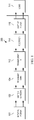
- FIG. 1 illustrates a block diagram of an LLC resonant converter in accordance with various embodiments of the present disclosure.
- the LLC resonant converter 200 is coupled between an input dc power source 101 and a load 111.
- the input dc power source 101 may be telecommunication power supplies converting a utility line voltage to a dc voltage.
- the input dc power source 101 may be a solar panel array.
- the input dc power source 101 may be an energy storage device such as rechargeable batteries, fuel cells and/or the like.
- the load 111 represents the power consumed by a circuit coupled to the LLC resonant converter 200.
- the load 111 may refer to downstream converters coupled to the output of the LLC resonant converter 200.
- the LLC resonant converter 200 may comprise a switch network 102, a resonant tank 104, a transformer 112, a rectifier 114 and an output filter 116. As shown in Figure 1 , the switch network 102, the resonant tank 104, the transformer 112, the rectifier 114 and the output filter 116 are coupled to each other and connected in cascade between the input dc power source 101 and the load 111.
- the switch network 102 may comprise primary side switches of a full bridge resonant converter according to some embodiments.
- the switch network 102 may be of the primary side switches of other bridge converters such as a half-bridge resonant converter, a push-pull resonant converter and the like.
- the detailed configuration of the switch network 102 will be described below with respect to Figure 2 .
- the resonant tank 104 may be implemented in a variety of ways.
- the main resonant tank comprises a series resonant inductor, a parallel resonant inductor and a series resonant capacitor (shown in Figure 2 respectively).
- the series resonant inductor and the parallel resonant inductor may be implemented as external inductors.
- the series resonant inductor may be implemented as a leakage inductance of the transformer 112.
- the resonant tank 104 includes three key resonant elements, namely the series resonant inductor, the series resonant capacitor and the parallel resonant inductor. Such a configuration is commonly referred to as an LLC resonant converter. According to the operating principle of LLC resonant converters, at a switching frequency approximately equal to the resonant frequency of the resonant tank 104, the resonant tank 104 helps to achieve zero voltage switching for the primary side switching elements and zero current switching for the secondary side switching elements.
- the LLC resonant converter 200 may further comprise a transformer 112, a rectifier 114 and an output filter 116.
- the transformer 112 provides electrical isolation between the primary side and the secondary side of the LLC resonant converter 200.
- the transformer 112 may be formed of two transformer windings, namely a primary transformer winding and a secondary transformer winding.
- the transformer 112 may have a center tapped secondary so as to have three transformer windings including a primary transformer winding, a first secondary transformer winding and a second secondary transformer winding.
- transformers described above and throughout the description are merely examples, which should not unduly limit the scope of the claims.
- the transformer 112 may further comprise a variety of bias windings and gate drive auxiliary windings.
- the rectifier 114 converts an alternating polarity waveform received from the output of the transformer 112 to a single polarity waveform.
- the rectifier 114 may be formed of a pair of switching elements such as n-type metal oxide semiconductor (NMOS) transistors.
- the rectifier 114 may be formed of a pair of diodes.
- the rectifier 114 may be a full-wave rectifier coupled to the single secondary winding of the transformer 112.
- the rectifier 114 may be formed by other types of controllable devices such as metal oxide semiconductor field effect transistor (MOSFET) devices, bipolar junction transistor (BJT) devices, super junction transistor (SJT) devices, insulated gate bipolar transistor (IGBT) devices, gallium nitride (GaN) based power devices and/or the like.
- MOSFET metal oxide semiconductor field effect transistor
- BJT bipolar junction transistor
- SJT super junction transistor
- IGBT insulated gate bipolar transistor
- GaN gallium nitride
- the output filter 116 is used to attenuate the switching ripple of the LLC resonant converter 200.
- the output filter 116 may be an L-C filter formed by an inductor and a plurality of capacitors.
- the output filter 116 may be an L-C filter formed by an inductor and a plurality of capacitors.
- some isolated dc/dc converter topologies such as forward converters may require an L-C filter.
- some isolated dc/dc converter topologies such as LLC resonant converters may include an output filter formed by a capacitor.
- different output filter configurations apply to different power converter topologies as appropriate.
- the configuration variations of the output filter 116 are within various embodiments of the present disclosure.
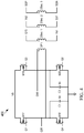
- FIG. 2 illustrates a schematic diagram of the LLC resonant converter shown in Figure 1 in accordance with various embodiments of the present disclosure.
- the switch network 102 includes four switching elements, namely Q1, Q2, Q3 and Q4. As shown in Figure 2 , a first pair of switching elements Q1 and Q2 are connected in series. A second pair of switching elements Q3 and Q4 are connected in series. The common node of the switching elements Q1 and Q2 is coupled to a first input terminal T1 of the resonant tank 104. Likewise, the common node of the switching elements Q3 and Q4 is coupled to a second input terminal T2 of the resonant tank 104.
- switching elements Q1, Q2, Q3 and Q4 form a primary side switching network of a full bridge resonant converter.
- switching elements Q1, Q2, Q3 and Q4 are implemented as MOSFET or MOSFETs connected in parallel, any combinations thereof and/or the like.
- the primary switches may be an insulated gate bipolar transistor (IGBT) device.
- the primary switches can be any controllable switches such as integrated gate commutated thyristor (IGCT) devices, gate turn-off thyristor (GTO) devices, silicon controlled rectifier (SCR) devices, junction gate field-effect transistor (JFET) devices, MOS controlled thyristor (MCT) devices, gallium nitride (GaN) based power devices and/or the like.
- IGCT integrated gate commutated thyristor
- GTO gate turn-off thyristor
- SCR silicon controlled rectifier
- JFET junction gate field-effect transistor
- MCT MOS controlled thyristor
- GaN gallium nitride
- the LLC resonant converter 200 shown in Figure 2 may have many variations, alternatives, and modifications.
- half bridge converters, push-pull converters may be alternatively employed.
- the full bridge resonant converter illustrated herein is limited solely for the purpose of clearly illustrating the inventive aspects of the various embodiments. The present invention is not limited to any particular power topology.
- Figure 2 illustrates four switches Q1, Q2, Q3, and Q4, various embodiments of the present disclosure may include other variations, modifications and alternatives.
- a separate capacitor may be connected in parallel with each switch of the primary side switching network. Such a separate capacitor helps to better control the timing of the resonant process of the LLC resonant converter 200.
- Figure 2 further illustrates the resonant tank 104 is coupled between the switch network 102 and the transformer 112.
- the resonant tank 104 is formed by a series resonant inductor Lr, a series resonant capacitor Cr1 and a parallel inductance Lm. As shown in Figure 2 , the series resonant inductor Lr and the series resonant capacitor Cr1 are connected in series and further coupled to the primary side of the transformer 112.
- Figure 2 shows the series resonant inductor Lr is an independent component
- the series resonant inductor Lr may be replaced by the leakage inductance of the transformer 112.
- the leakage inductance (not shown) may function as the series resonant inductor Lr.
- the transformer 112 may be of a primary winding and a center tapped secondary winding.
- the primary winding is coupled to terminals T3 and T4 of the resonant tank 104 as shown in Figure 2 .
- the secondary winding is coupled to the load 111 through the rectifier 114, which is formed by switches S1 and S2.
- the rectifier 114 formed by switches S1 and S2 may be alternatively referred to as a synchronous rectifier 114 throughout the description.
- the transformer structure shown in Figure 2 is merely an example.
- the secondary side of the transformer 112 may be a single winding.
- the secondary side may employ a synchronous rectifier formed by four switching elements (a.k.a. full wave rectifier).
- the operation principle of a synchronous rectifier coupled to a single secondary winding or a center tapped transformer secondary side is well known, and hence is not discussed in further detail herein.
- the power topology of the LLC resonant converter 200 may be not only applied to the rectifier as shown in Figure 2 , but also applied to other secondary configurations, such as voltage doubler rectifiers, current doubler rectifiers, any combinations thereof and/or the like.
- FIG. 2 further illustrates the LLC resonant converter 200 may comprise a driver 202.
- the driver 202 is capable of generating six gate drive signals for the primary switches Q1, Q2, Q3 and Q4, and the secondary switches S1 and S2. Since the driver 202 is able to provide gate drive signals for both the primary side switches and the secondary side switches, the driver 202 may comprise an isolation device such as a signal transformer and/or the like.
- the driver 202 is a lossless gate driver. Throughout the description, the driver 202 may be alternatively referred to as the lossless gate driver 202.
- driver 202 shown in Figure 2
- driver 202 providing drive signals for both the primary side and the secondary side
- other and alternate embodiment drivers could be employed (such as employing two separate drivers) and that other circuits, ( e . g ., lossless gate drive circuits, a pulse width modulation (PWM) gate drive circuits, etc.) could be employed for this function.
- PWM pulse width modulation
- FIG 3 illustrates a first illustrative implementation of the driver shown in Figure 2 in accordance with various embodiments of the present disclosure.
- the driver 300 is a lossless gate driver.
- the driver 300 is alternatively referred to as the lossless gate driver 300.
- the lossless gate driver 300 comprises an H-bridge 302, a resonant tank 304 and a signal transformer 306.
- the H-bridge 302 is formed by transistors M17, M18, M19 and M20.
- Transistor M17 and transistor M18 are connected in series between a bias voltage VB and ground.
- the common node of transistor M17 and transistor M18 is defined as G26 as shown in Figure 3 .
- G26 is used as a first low side gate drive signal ( e . g ., the gate drive signal for the switch Q2 shown in Figure 2 ).
- Transistor M19 and transistor M20 are connected in series between the bias voltage VB and ground.
- the common node of transistor M19 and transistor M20 is defined as G48 as shown in Figure 3 .
- G48 is used as a second low side gate drive signal ( e . g ., the gate drive signal for the switch Q4 shown in Figure 2 ).
- transistors M17, M18, M19 and M20 are implemented as N-channel MOSFETs, P-channel MOSFETs, any combinations thereof and/or the like.
- transistors M17 and M19 are driven by a plurality of narrow PWM pulses.
- the narrow PWM pulses are of a duty cycle from about 5% to about 25%. Alternatively, the duty cycle of the narrow PWM pulses may be less than 40%.
- Transistors M18 and M20 are driven by a plurality of wide PWM pulses.
- the wide PWM pulses are of a duty cycle approximately equal to 50%.
- the duty cycle of the transistors M17 and M19 may be adjustable. More particularly, in order to improve the gate drive speed of the switches of the LLC resonant converter 200, the duty cycle of the transistors M17 and M19 may be adjusted accordingly. In alternative embodiments, the duty cycle of the transistors M18 and M20 may be adjustable too in order to achieve better gate driving performance. The duty cycle of the transistors M18 and M20 may be adjusted to a range from about 40% to about 60%. It should be noted that the duty cycle of the transistors M18 and M20 is greater than the duty cycle of the transistors M17 and M19.
- the resonant tank 304 may comprise capacitor C1, the magnetizing inductance (not shown) of the signal transformer 306 and the parasitic gate capacitances (not shown) of the main power switches ( e . g ., Q1, Q2, Q3, Q4, S1 and S2 in Figure 2 ) of the LLC resonant converter 200.
- the capacitance of C1 is equal to 3 nF.
- the magnetizing inductance, the capacitor C1 and the parasitic capacitances may form a resonant process in which a resonant inductor current may charge and discharge the gate capacitors of the main power switches ( e . g ., Q1 in Figure 2 ) of the LLC resonant converter 200.
- the resonant tank 304 helps to return a portion of the energy at the gates of the main power switches to the source such as the bias voltage VB. As such, part of the gate drive energy is recovered so as to achieve lossless gate driving.
- the capacitor C36 is not part of the resonant tank 304.
- the capacitor C36 helps to balance the magnetic flux of the signal transformer 306.
- the capacitance of C36 is equal to 100 nF.
- the signal transformer 306 comprises a primary winding DPri, a first secondary winding DSec_1, a second secondary winding DSec_2 and a third secondary winding DSec_3.
- the output voltage across G15 and Vs1 is used to drive a first high side switch ( e . g ., switch Q1 shown in Figure 2 ).
- the output voltage across G37 and Vs2 is used to drive a second high side switch ( e . g ., switch Q3 shown in Figure 2 ).
- Signals SGP and SGN are used to drive the secondary switches S1 and S2 respectively. It should be noted while Figure 3 shows G26 is used as the first low side gate drive signal ( e .
- the gate drive signal for the switch Q2 shown in Figure 2 and G48 is used as a second low side gate drive signal ( e . g ., the gate drive signal for the switch Q4 shown in Figure 2 ), the low side switches such as Q2 and Q4 in Figure 2 can be driven by a winding such as DSec_1 and DSec_2 shown in Figure 3 .
- the output voltages at G15 and G37 can be used to drive low side switches.
- the gate drive voltage rating (e . g ., the turn-on threshold voltage) of the low side switches, high side switches and the secondary side switches is related to the turns ratio of the signal transformer 306.
- the gate drive turn-on threshold voltage of the low side switches such as Q2 and Q4 is defined as Vth_PS_L.
- the gate drive turn-on threshold voltage of the first high side switch such as Q1 is defined as Vth_PS_H1.
- the gate drive turn-on threshold voltage of the second high side switch such as Q3 is defined as Vth_PS_H2.
- the gate drive turn-on threshold voltage of the secondary side switches such as S1 and S2 is defined as Vth_SS.
- the turns ratio (Dpri/DSec_1/DSec_2) of the signal transformer 306 is approximately equal to Vth_PS_L/Vth_PS_H1/Vth_PS_H2.
- the turns ratio (Dpri/DSec_3) is greater than or equal to Vth_PS_L/Vth_SS.
- the bias voltage VB is not fixed.
- the voltage level of VB may vary depending on different operating modes. For example, VB may change during a startup process of the LLC resonant converter 200. Furthermore, VB may vary in response to different load conditions. VB may be of a low voltage level when the LLC resonant converter 200 operates at a light load condition. On the other hand, VB may be of a high voltage level when the LLC resonant converter 200 operates at a full/heavy load condition.
- FIG 4 illustrates a second illustrative implementation of the driver shown in Figure 2 in accordance with various embodiments of the present disclosure.
- the driver 400 shown in Figure 4 is similar to the driver 300 shown in Figure 3 except that the capacitor C1 shown in Figure 3 is replaced by two capacitors.
- a first capacitor C1 is connected in parallel with the transistor M18.
- a second capacitor C3 is connected in parallel with the transistor M20.
- the capacitance of the first capacitor C1 is equal to the capacitance of the second capacitor C3.
- the capacitance of the first capacitor C1 is equal to 6 nF.
- the capacitance of the second capacitor C2 is equal to 6 nF.
- the magnetizing inductance, the first capacitor C1, the second capacitor C3 and the parasitic capacitances of the main power switches may form a resonant process in which a resonant inductor current may charge and discharge the gate capacitors of the main power switches ( e . g ., Q1 in Figure 2 ).
- the resonant tank formed by C1, C3, the magnetizing inductance and the parasitic capacitances may help to return a portion of the energy at the gates of the main power switches to the source such as the bias voltage VB. As such, part of the gate drive energy is recovered so as to achieve lossless gate driving.
- FIG. 4 shows C1 is connected in parallel with the transistor M18 and C3 is connected in parallel with the transistor M20.
- C1 and C3 may be in parallel with transistors M17 and M19 respectively.
- C1 may be in parallel with M17 and C3 may be in parallel with M20.
- C1 may be in parallel with M18 and C3 may be in parallel with M19.
- FIG. 5 illustrates a third illustrative implementation of the driver shown in Figure 2 in accordance with various embodiments of the present disclosure.
- the driver 500 shown in Figure 5 is similar to the driver 400 shown in Figure 4 except that the first capacitor C1 and the second capacitor C3 are connected in parallel with the transistor M17 and transistor M19 respectively.
- the capacitance of the first capacitor C1 is equal to 6 nF.
- the capacitance of the second capacitor C2 is equal to 6 nF.
- the operation principle of the driver 500 is similar to that of the driver 400 shown in Figure 4 , and hence is not discussed in further detail to avoid unnecessary repetition.
- FIG. 6 illustrates a fourth illustrative implementation of the driver shown in Figure 2 in accordance with various embodiments of the present disclosure.
- the driver 600 shown in Figure 6 is similar to the driver 400 shown in Figure 4 except that the first capacitor C1 and the second capacitor C3 are connected in series with the transistor M15 and the transistor M24 respectively. Since the first capacitor C1 is switchable through turning on/off the transistor M15, the series-connected C1 and M15 is alternatively referred to a switchable capacitor C1. Likewise, the series-connected C3 and M24 is alternatively referred to a switchable capacitor C3 throughout the description.
- Figure 6 shows a single switchable capacitor (e . g ., switchable capacitor C1) is connected in parallel with the transistor ( e . g ., transistor M1)
- the driver 600 may accommodate any number of switchable capacitors. In other words, there may be a plurality of switchable capacitors are connected in parallel with the transistor ( e . g ., M18 and M20) of the driver 600.
- the actual capacitance connected to each transistor may vary through turning on/off the switches ( e . g ., M15 and M24).
- the resonance process of the driver 600 may be fine-tuned so as to match the resonant frequency of the resonant tank 104 of the LLC resonant converter 200.
- Figure 6 shows the switchable capacitor C1 is connected in parallel with the transistor M18 and the switchable capacitor C3 is connected in parallel with the transistor M20.
- the switchable capacitors C1 and C3 may be in parallel with transistors M17 and M19 respectively.
- the switchable capacitor C1 may be in parallel with M17 and the switchable capacitor C3 may be in parallel with M20.
- the switchable capacitor C1 may be in parallel with M18 and the switchable capacitor C3 may be in parallel with M19.
- the capacitor C12 can be replaced by a switchable capacitor such as the switchable capacitor C1.
- a switchable capacitor can be connected in parallel with the capacitor C12.
- FIG. 7 illustrates a fifth illustrative implementation of the driver shown in Figure 2 in accordance with various embodiments of the present disclosure.
- the driver 700 shown in Figure 7 is similar to the driver 400 shown in Figure 4 except that the capacitors C6 and C9 are added into one of the secondary side winding of the signal transformer.
- the capacitance of the first capacitor C6 is equal to 47 nF.
- the capacitance of the second capacitor C9 is equal to 47 nF.
- capacitors C6 and C9 are connected in series with the secondary side winding DSec_3.
- a resistor (not shown) connected in parallel with the capacitor (e.g., capacitor C6).
- the capacitors C6 and C9 may function as a divider, through which the gate drive voltage level and speed may be controlled accordingly.
- the divider formed by C6 and C9 may help to provide an appropriate gate drive voltage when an exact turns ratio of the signal transformer is not viable.
- the turns ratio (Dpri/DSec_3) of the signal transformer 306 equal to Vth_PS_L/Vth_SS.
- the divider is introduced to further fine-tune the voltage applied to the gates of the power switches so that the gate drive voltages at the outputs of the driver match their respective turn-on threshold voltages of the LLC resonant converter 200. It should be noted that this technique is applicable to the gate driving windings for the primary side switches if needed.
- FIG 8 illustrates a sixth illustrative implementation of the driver shown in Figure 2 in accordance with various embodiments of the present disclosure.
- the driver 800 shown in Figure 8 is similar to the driver 700 shown in Figure 7 except that two additional capacitors C10 and C11 are added into the secondary side windings DSec_1 and DSec_2 respectively.
- the capacitance of the first capacitor C10 is equal to 47 nF.
- the capacitance of the second capacitor C11 is equal to 47 nF.
- the capacitors C10 and C11 may function as a divider, through which the gate drive speed may be controlled accordingly.
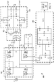
- FIG. 9 illustrates a schematic diagram of a lossless gate drive circuit having a maximum efficiency point tracking (MEPT) control mechanism in accordance with various embodiments of the present disclosure.
- the lossless gate drive circuit 900 includes an H-bridge 901, a resonant device, a signal transformer 903, a secondary stage 905, a MEPT detector 902 and a control circuit 904.
- the H-bridge 901 includes four switches, namely Q1, Q2, Q3 and Q4.
- the connection and the operating principle of these four switches are similar to those shown in Figure 3 , and hence are not discussed herein.
- the resonant device may comprise a fixed capacitance, parasitic capacitances of the power switches (not shown) coupled to the outputs of the lossless gate drive circuit 900, an inductor L4 and an adjustable capacitance.
- the fixed capacitance is formed by a capacitor C6 and a capacitor C8. As shown in Figure 9 , the capacitor C6 is connected in parallel with the switch Q3. The capacitor C8 is connected in parallel with the switch Q2.
- the fixed capacitance of the lossless gate drive circuit 900 shown in Figure 9 is merely an example.
- Other configurations of the capacitors such as the fixed capacitance configurations shown in Figures 3-8 are also within the contemplated scope of the invention.
- the adjustable capacitance may be implemented as a plurality of capacitors connected in parallel with the capacitor C8. More particularly, each capacitor (e . g ., capacitor Cn) is connected in series with an auxiliary switch ( e . g ., Sn) to form a switchable capacitor. When the auxiliary switch is turned on, the switchable capacitor is connected in parallel with the capacitor C8. As a result, the total capacitance of the resonant device is increased. On the other hand, when the auxiliary switch is turned off, the switchable capacitor is disconnected from the resonant device. As a result, the total capacitance of the resonant device is reduced.
- capacitors there may be a plurality of capacitors and their respective auxiliary switches are connected in parallel with the capacitor C8.
- the capacitance of the capacitor C8 is equal to 1 nF.
- a plurality of switchable capacitors may form a switchable capacitor bank, which is connected in parallel with the capacitor C8. By turning on/off the auxiliary switches of the switchable capacitor bank, a variety of capacitances can be obtained.
- switchable capacitor bank of the lossless gate drive circuit 900 shown in Figure 9 is merely an example.
- Other configurations of the switchable capacitor bank are also within the contemplated scope of the invention.
- the switchable capacitor bank may be connected in parallel with the capacitor C6.
- two switchable capacitor banks may be connected in parallel with the capacitor C6 and the capacitor C8 respectively.
- the magnetizing inductance of the signal transformer 903 is about 1.1 uH.
- the signal transformer 903 may further comprise a leakage inductance (not shown) connected in series with the primary side of the signal transformer 903.
- the signal transformer 903 includes a primary winding L1, a first secondary winding L2 and a second secondary winding L3.
- the turns ratio of the signal transformer 902 is 5:3 in accordance with some embodiments.
- the secondary stage 905 has inputs coupled to the secondary windings L2 and L3 of the signal transformer 903 respectively and outputs Vgs31 and Vgs32 coupled to the gates of a synchronous rectifier of an LLC resonant converter 200 respectively.
- the secondary stage 905 includes resistors R1, R2, R3, R4, R13 and R4, and capacitors C3, C4, C17 and C18. As shown in Figure 9 , C3, C17, R3 and R13 may form a first divider, through which the gate drive voltage Vgs31 may be adjusted depending on different applications and design needs. Likewise, C4, C18, R4 and R14 may form a second divider, through which the gate drive voltage Vgs32 may be adjusted depending on different applications and design needs.
- the MEPT detector 902 detects a voltage signal across node A and node B.
- the resonant frequency of the lossless gate drive circuit 900 is approximately equal to the switching frequency of the resonant tank of the LLC resonant converter 200, the magnitude of the voltage across node A and node B is reduced.
- the resonant frequency of the lossless gate drive circuit 900 is away from the switching frequency of the resonant tank of the LLC resonant converter 200, the magnitude of the voltage across node A and node B is increased.
- the MEPT detector 902 detects the voltage across node A and node B.
- the MEPT detector 902 sends the detected signal to the control circuit 904.
- the control circuit 904 compares the detected signal with a predetermined threshold or finds a lowest point of the detected signal.
- the lowest point of the detected signal indicates the resonant frequency of driver is approximately equal to the switch frequency of the resonant converter. If the detected signal is greater than the lowest point, the control circuit 904 adjusts the resonant frequency of the driver through turning on/off the switchable capacitors until the resonant frequency of driver approximately matches the switch frequency of the resonant converter. As a result, the lossless gate drive circuit 900 is forced to operate at a resonant frequency close to the switching frequency of the LLC resonant converter 200. Such a resonant frequency helps the LLC resonant converter as well as the lossless gate drive circuit 900 achieve higher efficiency.
- the MEPT detector 902 and the control circuit 904 may form an adaptive control loop.
- Such an adaptive control loop helps the lossless gate drive circuit 900 operate at a resonant frequency matching the switching frequency of the LLC resonant converter 200.
- the control circuit 904 may force the lossless gate drive circuit 900 to operate at a resonant frequency close to the switching frequency of the LLC resonant converter 200 based upon the real-time detected signal from the MEPT detector 902.
- the lossless gate drive circuit 900 is capable of dynamically adjust its resonant frequency so that the lossless gate drive circuit 900 as well as the LLC resonant converter 200 can achieve higher efficiency.
- the MEPT detector 902 includes a rectifier, decoupling capacitors C5 and C7, a load resistor R1 and a divider/filter circuit.
- the rectifier as shown in Figure 9 , includes C1, C2, D1 and D2. The rectifier is employed to convert the ac voltage across node A and node B into a dc voltage.
- the divider/filter circuit includes R2, R3 and C3.
- R2 and R3 form a voltage divider.
- An appropriate dc voltage signal is fed into the control circuit 904 through adjusting the ratio of R2 to R3.
- C3, R2 and R3 may form a filter to attenuate noise so that the control circuit 904 may receive a noise free dc signal.
- the resistance of R1 is equal to 330 ohm.
- the capacitance of C1 is equal to 1 nF.
- the capacitance of C2 is equal to 1 nF.
- the capacitance of C3 is equal to 2 nF.
- the capacitance of C5 is equal to 30 pF.
- the capacitance of C7 is equal to 30 pF.
- the resistance of R2 is equal to 20 Kohm.
- the resistance of R3 is equal to 2 Kohm.
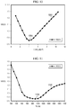
- Figure 10 illustrates a resonant process detection curve of the lossless gate drive circuit in Figure 9 in accordance with various embodiments of the present disclosure.
- the horizontal axis of Figure 10 represents the capacitance of the resonant device of the lossless gate drive circuit 900.
- the vertical axis represents the output voltage VS3 (shown in Figure 9 ) at the output of the MEPT detector 902.
- the curve 1002 illustrates the output voltage VS3 of the MEPT detector 902.
- the output voltage VS3 may reach its lowest point 1004 when the capacitance of the resonant device is about 4 nF.
- the lowest point 1004 shown in Figure 10 indicates the resonant frequency of the lossless gate drive circuit 900 is approximately equal to the switching frequency of the LLC resonant converter 200. In other words, the LLC resonant converter 200 and the lossless gate drive circuit 900 may achieve high efficiency when the output voltage VS3 reaches its lowest point 1004.
- a digital signal processor may be employed to find the lowest point of VS3 and obtain the necessary capacitance through turning on/off the auxiliary switches shown in Figure 9 .
- Figure 11 illustrates another resonant process detection curve of the lossless gate drive circuit in Figure 9 in accordance with various embodiments of the present disclosure.
- the horizontal axis of Figure 11 represents the switching period of the lossless gate drive circuit 900.
- the unit of the horizontal axis is nS.
- the vertical axis represents the voltage at the output voltage VS3 of the MEPT detector 902.
- the curve 1102 illustrates the voltage at the output voltage VS3 of the MEPT detector 902.
- the output voltage VS3 may reach its lowest point 1104 when the switching period of the lossless gate drive circuit 900 is about 990 nS.
- the lowest point 1104 shown in Figure 11 indicates the resonant frequency of the lossless gate drive circuit 900 is approximately equal to the switching frequency of the LLC resonant converter 200.
- the method of finding the lowest point 1104 and adjusting the capacitance of the resonant device is similar to that shown in Figure 10 , and hence is not discussed herein.
- Figure 12 illustrates switching waveforms of the lossless gate drive circuit in Figure 9 in accordance with various embodiments of the present disclosure.
- the horizontal axis of Figure 12 represents intervals of time.
- the unit of the horizontal axis is micro second.
- the first vertical axis Y1 represents a first group of gate drive signals of the H-bridge of the lossless gate drive circuit.
- the second vertical axis Y2 represents a second group of gate drive signals of the H-bridge of the lossless gate drive circuit.
- the third vertical axis Y3 represents low-side gate drive signals of the LLC resonant converter 200.
- the fourth vertical axis Y4 represents high-side gate drive signals of the LLC resonant converter 200.
- the fifth vertical axis Y5 represents secondary gate drive signals of the LLC resonant converter 200.
- waveform 1202 is the gate drive signal of the transistor M19 shown in Figure 3 .
- Waveform 1204 is the gate drive signal of the transistor M18 shown in Figure 3 .
- Waveform 1212 is the gate drive signal of the transistor M20 shown in Figure 3 .
- Waveform 1214 is the gate drive signal of the transistor M17 shown in Figure 3 .
- waveform 1202 shows the duty cycle of the gate drive signal of the transistor M19 is in a range from about 5% to about 25%.
- Waveform 1204 shows the duty cycle of the gate drive signal of the transistor M18 is approximately equal to 50%.
- Waveform 1214 shows the duty cycle of the gate drive signal of the transistor M17 is in a range from about 5% to about 25%.
- Waveform 1212 shows the duty cycle of the gate drive signal of the transistor M20 is approximately equal to 50%.
- waveform 1222 shows the signal G26 shown in Figure 3 .
- G26 is used to drive a first low-side switch of the LLC resonant converter 200 ( e . g ., the switch Q2 shown in Figure 2 ).
- Waveform 1224 shows the signal G46 shown in Figure 3 .
- G46 is used to drive a second low-side switch of the LLC resonant converter 200 ( e . g ., the switch Q4 shown in Figure 2 ).
- waveform 1232 shows the signal G37 shown in Figure 3 .
- G37 is used to drive a first high-side switch of the LLC resonant converter 200 ( e . g ., the switch Q1 shown in Figure 2 ).
- Waveform 1234 shows the signal G15 shown in Figure 3 .
- G15 is used to drive a second high-side switch of the LLC resonant converter 200 ( e . g ., the switch Q3 shown in Figure 2 ).
- waveform 1242 shows the signal across node SGP and node SGN shown in Figure 3 .
- SGP and SGN are used to drive the switches of the rectifier ( e . g ., switches S1 and S2 shown in Figure 2 ).
Landscapes
- Engineering & Computer Science (AREA)
- Power Engineering (AREA)
- Dc-Dc Converters (AREA)
- Power Conversion In General (AREA)
Description
- The present invention relates to a resonant converter, and, in particular embodiments, to a lossless gate driver of resonant converters.
- A telecommunication network power system usually includes an AC-DC stage converting the power from the AC utility line to a 48V DC distribution bus and a DC-DC stage converting the 48V DC distribution bus to a plurality of voltage levels for all types of telecommunication loads. Both stages may comprise isolated DC-DC converters. Isolated DC-DC converters can be implemented by using different power topologies, such as flyback converters, forward converters, half bridge converters, full bridge converters, inductor-inductor-capacitor (LLC) resonant converters and the like.
- As technologies further advance, bus converters have been widely employed in the telecommunication industry. The bus voltages may be divided into three categories, a 12V bus voltage converted from a 48V input dc power supply, a 48V bus voltage converted from a 380V input dc power supply and a 12V bus voltage converted from a 380V input dc power supply. A bus converter not only converts the input voltage from a higher level to a lower level, but also provides isolation through a magnetic device such as transformers and/or the like.
- The intermediate bus voltage such as 12V may function as an input power bus for a plurality of downstream non-isolated power converters. The downstream non-isolated power converters may be implemented as step-down dc/dc converters such as buck converters, step-up dc/dc converters such as boost converters, linear regulators, any combinations thereof and/or the like. The downstream non-isolated power converters operate under a tight control loop so that fully regulated output voltages are fed into their respective loads.
- As power consumption has become more important, there may be a need for high power density and high efficiency bus converters. LLC resonant converters have become the preferred choice for achieving high performance (e.g., high power density and high efficiency) because LLC resonant converters are capable of reducing switching losses through zero voltage switching and/or zero current switching.
-
WO 2006/079219 A1 discloses a resonate gate drive circuit, wherein the resonate gate drive circuit for driving at least one power switching device recovers energy loss for charging and discharging the gate capacitance of the power switching devices. The gate drive circuit uses a current source to charge and discharge the gate capacitance with a high current, reducing the switching loss of the power switching device. The gate drive circuit comprises four semiconductor bidirectional conducting switching devices connected in a full-bridge configuration. An inductor connected across the bridge configuration provides the current source. The gate drive circuit may be used in single and dual high-side and low-side, symmetrical or complementary, power converter gate drive applications. -
WO 2013/046420 A1 discloses a semiconductor drive circuit of a switching element. In the semiconductor drive circuit, an arm has a drain terminal of a switching element of an upper arm connected to a positive electrode of a first power supply, a source terminal of a switching element of a lower arm connected to a negative electrode of the first power supply, and the source terminal of the switching element of the upper arm and the drain terminal of the switching element of the lower arm connected to each other. Each of the gate drive circuits provided by a unit of the switching element includes an FET circuit, and a parallel circuit, wherein a first resistor and a first capacitor are connected in parallel, and a first terminal is connected to the gate terminal of the switching element. The FET circuit has a second terminal of the parallel circuit connected to the source terminal thereof, one end of a second capacitor connected to the gate terminal thereof, a second resistor connected to between the drain terminal and the gate terminal, and has a second power supply connected to between the drain terminal and the other terminal of the second capacitor. The second power supply is a three-level power supply having levels thereof configured of zero potential, a positive value and a negative value, and is an alternating current power supply that includes a period having zero potential between the positive value and the negative value. The second power supply is configured such that, during a period when the positive value is applied to one of the gate drive circuits, the negative value is applied to the other one of the gate drive circuits, and in the second power supply, the other end of the second capacitor, said the other end being connected to the gate terminal of the FET circuit, is connected to the source terminal of the switching element. -
WO 2013/106692 A1 discloses a resonant power converter, wherein the resonant power converter is provided with auxiliary circuit branches and control circuitry for switchably coupling the auxiliary branches to resonant circuit components during holdup times. Auxiliary branches are coupled in parallel with any one or more of a resonant inductor, a resonant capacitor, and a magnetizing inductive winding via respective switches. When a holdup time condition is detected in accordance with, for example, a drop in the mains line voltage, the switches are controlled to adjust the corresponding inductance or capacitance for the duration of the holdup time condition or otherwise for a predetermined duration. The power converter in normal operation is configured for high efficiency and in a holdup time operation is configured to produce sufficient holdup time. - These and other problems are generally solved or circumvented, and technical advantages are generally achieved, by preferred embodiments of the present invention which provide a lossless gate drive circuit for an inductor-inductor-capacitor (LLC) resonant power converter.
In accordance with an embodiment, in a driver for generating gate drive signals for a plurality of switches of an inductor-inductor-capacitor (LLC) resonant converter, the LLC resonant converter comprising: a switching network comprising a first driver switch and a second driver switch connected in series and a third driver switch and a fourth driver switch connected in series; and a resonant tank connected between the switching network and a primary side of a transformer; and a rectifier coupled to a secondary side of the transformer;
and in the driver coupled to the switching network and the rectifier, the driver comprises a bridge coupled between a bias voltage and ground, wherein the bridge comprises a first switch and a second switch connected in series and coupled between the bias voltage and ground and a third switch and a fourth switch connected in series and coupled between the bias voltage and ground, a resonant device coupled to the bridge, wherein the resonant device comprises a fixed capacitance, a gate capacitance and a magnetizing inductance. The resonant device also comprises an adjustable capacitance, the adjustable capacitance may be implemented as a plurality of capacitors, each capacitor is connected in series with an auxiliary switch to form a switchable capacitor, a transformer coupled to the resonant device, wherein the transformer comprises a primary winding and a plurality of secondary windings. Wherein the driver further comprises a MEPT detector and a control circuit; the MEPT detector is configured to detect the voltage across node A and node B, and send the detected signal to the control circuit; wherein the node B is the first common node, and the node A is the second common node; and the control circuit is configured to adjust the resonant frequency of the driver through turning on/off the switchable capacitors until the resonant frequency of driver approximately matches the switch frequency of the resonant converter, if the detected signal is greater than a lowest point. The LLC resonant converter comprises a first driver switch and a second driver switch connected in series and a third driver switch and a fourth driver switch connected in series, and a resonant tank connected between the switching network and a primary side of a transformer,and a rectifier coupled to a secondary side of the transformer. - In accordance with another embodiment, a system comprises a resonant converter comprising a switching network comprising a first driver switch and a second driver switch connected in series and a third driver switch and a fourth driver switch connected in series, a resonant tank connected between the switching network and a primary side of a transformer and a rectifier coupled to a secondary side of the transformer.
- The system further comprises a driver coupled to the resonant converter, wherein the driver comprises a bridge coupled between a bias voltage and ground, wherein the bridge comprises a first driver switch and a second driver switch connected in series and coupled between the bias voltage and ground and a third driver switch and a fourth driver switch connected in series and coupled between the bias voltage and ground, a resonant device coupled to the bridge, wherein the resonant device comprises a fixed capacitance, a magnetizing inductance and gate capacitances of the switching network and the rectifier and a signal transformer coupled to the resonant device, wherein the signal transformer comprises a primary winding and a plurality of secondary windings.
- In accordance with yet another embodiment, a method providing a resonant converter comprising a switching network comprising a first high-side switch, a second high-side switch, a first low-side switch and a second low-side switch, a resonant tank coupled between the switching network and a transformer and a rectifier coupled to a secondary side of the transformer.
The method further comprises coupling a driver to the switching network and the rectifier, wherein the driver includes a first winding coupled to the rectifier, a second winding coupled to the first high-side switch and a third winding coupled to the second high-side switch, detecting a signal indicating a soft switching process of the driver and adjusting a resonant frequency of the driver until the resonant frequency of the driver approximately matches a switch frequency of the resonant converter. The step of adjusting a resonant frequency of the driver until the resonant frequency of the driver approximately matches a switch frequency of the resonant converter, comprising:
adjusting the resonant frequency of the driver through turning on/off the switchable capacitors until the resonant frequency of driver approximately matches the switch frequency of the resonant converter, if the detected signal is greater than a lowest point. - An advantage of a preferred embodiment of the present invention is improving the efficiency of an LLC resonant converter through a lossless gate drive circuit.
- The foregoing has outlined rather broadly the features and technical advantages of the present invention in order that the detailed description of the invention that follows may be better understood. Additional features and advantages of the invention will be described hereinafter which form the subject of the claims of the invention. It should be appreciated by those skilled in the art that the conception and specific embodiment disclosed may be readily utilized as a basis for modifying or designing other structures or processes for carrying out the same purposes of the present invention.
- For a more complete understanding of the present invention, and the advantages thereof, reference is now made to the following descriptions taken in conjunction with the accompanying drawings, in which:
-
Figure 1 illustrates a block diagram of an LLC resonant converter in accordance with various embodiments of the present disclosure; -
Figure 2 illustrates a schematic diagram of the LLC resonant converter shown inFigure 1 in accordance with various embodiments of the present disclosure; -
Figure 3 illustrates a first illustrative implementation of the driver shown inFigure 2 in accordance with various embodiments of the present disclosure; -
Figure 4 illustrates a second illustrative implementation of the driver shown inFigure 2 in accordance with various embodiments of the present disclosure; -
Figure 5 illustrates a third illustrative implementation of the driver shown inFigure 2 in accordance with various embodiments of the present disclosure; -
Figure 6 illustrates a fourth illustrative implementation of the driver shown inFigure 2 in accordance with various embodiments of the present disclosure; -
Figure 7 illustrates a fifth illustrative implementation of the driver shown inFigure 2 in accordance with various embodiments of the present disclosure; -
Figure 8 illustrates a sixth illustrative implementation of the driver shown inFigure 2 in accordance with various embodiments of the present disclosure; -
Figure 9 illustrates a schematic diagram of a lossless gate drive circuit having a maximum efficiency point tracking (MEPT) control mechanism in accordance with various embodiments of the present disclosure; -
Figure 10 illustrates a resonant process detection curve of the lossless gate drive circuit inFigure 9 in accordance with various embodiments of the present disclosure; -
Figure 11 illustrates another resonant process detection curve of the lossless gate drive circuit inFigure 9 in accordance with various embodiments of the present disclosure; and -
Figure 12 illustrates switching waveforms of the lossless gate drive circuit inFigure 9 in accordance with various embodiments of the present disclosure. - Corresponding numerals and symbols in the different figures generally refer to corresponding parts unless otherwise indicated. The figures are drawn to clearly illustrate the relevant aspects of the various embodiments and are not necessarily drawn to scale.
- The making and using of the presently preferred embodiments are discussed in detail below. It should be appreciated, however, that the present invention provides many applicable inventive concepts that can be embodied in a wide variety of specific contexts. The specific embodiments discussed are merely illustrative of specific ways to make and use the invention, and do not limit the scope of the invention.
- The present invention will be described with respect to preferred embodiments in a specific context, namely a lossless gate driver for an inductor-inductor-capacitor (LLC) resonant converter. The invention may also be applied, however, to a variety of resonant converters. Hereinafter, various embodiments will be explained in detail with reference to the accompanying drawings.
-
Figure 1 illustrates a block diagram of an LLC resonant converter in accordance with various embodiments of the present disclosure. The LLCresonant converter 200 is coupled between an inputdc power source 101 and aload 111. The inputdc power source 101 may be telecommunication power supplies converting a utility line voltage to a dc voltage. Alternatively, the inputdc power source 101 may be a solar panel array. Furthermore, the inputdc power source 101 may be an energy storage device such as rechargeable batteries, fuel cells and/or the like. Theload 111 represents the power consumed by a circuit coupled to the LLCresonant converter 200. Alternatively, theload 111 may refer to downstream converters coupled to the output of the LLCresonant converter 200. - The LLC
resonant converter 200 may comprise aswitch network 102, aresonant tank 104, atransformer 112, arectifier 114 and anoutput filter 116. As shown inFigure 1 , theswitch network 102, theresonant tank 104, thetransformer 112, therectifier 114 and theoutput filter 116 are coupled to each other and connected in cascade between the inputdc power source 101 and theload 111. - The
switch network 102 may comprise primary side switches of a full bridge resonant converter according to some embodiments. Alternatively, theswitch network 102 may be of the primary side switches of other bridge converters such as a half-bridge resonant converter, a push-pull resonant converter and the like. The detailed configuration of theswitch network 102 will be described below with respect toFigure 2 . - The
resonant tank 104 may be implemented in a variety of ways. For example, the main resonant tank comprises a series resonant inductor, a parallel resonant inductor and a series resonant capacitor (shown inFigure 2 respectively). - The series resonant inductor and the parallel resonant inductor may be implemented as external inductors. A person skilled in the art will recognize that there may be many variation, alternatives and modifications. For example, the series resonant inductor may be implemented as a leakage inductance of the
transformer 112. - In sum, the
resonant tank 104 includes three key resonant elements, namely the series resonant inductor, the series resonant capacitor and the parallel resonant inductor. Such a configuration is commonly referred to as an LLC resonant converter. According to the operating principle of LLC resonant converters, at a switching frequency approximately equal to the resonant frequency of theresonant tank 104, theresonant tank 104 helps to achieve zero voltage switching for the primary side switching elements and zero current switching for the secondary side switching elements. - The LLC
resonant converter 200 may further comprise atransformer 112, arectifier 114 and anoutput filter 116. Thetransformer 112 provides electrical isolation between the primary side and the secondary side of the LLCresonant converter 200. In accordance with an embodiment, thetransformer 112 may be formed of two transformer windings, namely a primary transformer winding and a secondary transformer winding. Alternatively, thetransformer 112 may have a center tapped secondary so as to have three transformer windings including a primary transformer winding, a first secondary transformer winding and a second secondary transformer winding. - It should be noted that the transformers described above and throughout the description are merely examples, which should not unduly limit the scope of the claims. One of ordinary skill in the art would recognize many variations, alternatives, and modifications. For example, the
transformer 112 may further comprise a variety of bias windings and gate drive auxiliary windings. - The
rectifier 114 converts an alternating polarity waveform received from the output of thetransformer 112 to a single polarity waveform. When thetransformer 112 is of a center tapped secondary, therectifier 114 may be formed of a pair of switching elements such as n-type metal oxide semiconductor (NMOS) transistors. Alternatively, therectifier 114 may be formed of a pair of diodes. On the other hand, when thetransformer 112 is of a single secondary winding, therectifier 114 may be a full-wave rectifier coupled to the single secondary winding of thetransformer 112. - Furthermore, the
rectifier 114 may be formed by other types of controllable devices such as metal oxide semiconductor field effect transistor (MOSFET) devices, bipolar junction transistor (BJT) devices, super junction transistor (SJT) devices, insulated gate bipolar transistor (IGBT) devices, gallium nitride (GaN) based power devices and/or the like. The detailed operation and structure of therectifier 114 are well known in the art, and hence are not discussed herein. - The
output filter 116 is used to attenuate the switching ripple of the LLCresonant converter 200. According to the operation principles of isolated dc/dc converters, theoutput filter 116 may be an L-C filter formed by an inductor and a plurality of capacitors. One person skilled in the art will recognize that some isolated dc/dc converter topologies such as forward converters may require an L-C filter. On the other hand, some isolated dc/dc converter topologies such as LLC resonant converters may include an output filter formed by a capacitor. One person skilled in the art will further recognize that different output filter configurations apply to different power converter topologies as appropriate. The configuration variations of theoutput filter 116 are within various embodiments of the present disclosure. -
Figure 2 illustrates a schematic diagram of the LLC resonant converter shown inFigure 1 in accordance with various embodiments of the present disclosure. Theswitch network 102 includes four switching elements, namely Q1, Q2, Q3 and Q4. As shown inFigure 2 , a first pair of switching elements Q1 and Q2 are connected in series. A second pair of switching elements Q3 and Q4 are connected in series. The common node of the switching elements Q1 and Q2 is coupled to a first input terminal T1 of theresonant tank 104. Likewise, the common node of the switching elements Q3 and Q4 is coupled to a second input terminal T2 of theresonant tank 104. - The switching elements Q1, Q2, Q3 and Q4 form a primary side switching network of a full bridge resonant converter. According to some embodiments, switching elements Q1, Q2, Q3 and Q4 are implemented as MOSFET or MOSFETs connected in parallel, any combinations thereof and/or the like.
- According to alternative embodiments, the primary switches (e.g., switch Q1) may be an insulated gate bipolar transistor (IGBT) device. Alternatively, the primary switches can be any controllable switches such as integrated gate commutated thyristor (IGCT) devices, gate turn-off thyristor (GTO) devices, silicon controlled rectifier (SCR) devices, junction gate field-effect transistor (JFET) devices, MOS controlled thyristor (MCT) devices, gallium nitride (GaN) based power devices and/or the like.
- It should be noted that while the example throughout the description is based upon a full bridge LLC resonant converter (e.g., full bridge LLC resonant converter shown in
Figure 2 ), the LLCresonant converter 200 shown inFigure 2 may have many variations, alternatives, and modifications. For example, half bridge converters, push-pull converters may be alternatively employed. The full bridge resonant converter illustrated herein is limited solely for the purpose of clearly illustrating the inventive aspects of the various embodiments. The present invention is not limited to any particular power topology. - It should further be noted that while
Figure 2 illustrates four switches Q1, Q2, Q3, and Q4, various embodiments of the present disclosure may include other variations, modifications and alternatives. For example, a separate capacitor may be connected in parallel with each switch of the primary side switching network. Such a separate capacitor helps to better control the timing of the resonant process of the LLCresonant converter 200. -
Figure 2 further illustrates theresonant tank 104 is coupled between theswitch network 102 and thetransformer 112. Theresonant tank 104 is formed by a series resonant inductor Lr, a series resonant capacitor Cr1 and a parallel inductance Lm. As shown inFigure 2 , the series resonant inductor Lr and the series resonant capacitor Cr1 are connected in series and further coupled to the primary side of thetransformer 112. - It should be noted while
Figure 2 shows the series resonant inductor Lr is an independent component, the series resonant inductor Lr may be replaced by the leakage inductance of thetransformer 112. In other words, the leakage inductance (not shown) may function as the series resonant inductor Lr. - The
transformer 112 may be of a primary winding and a center tapped secondary winding. The primary winding is coupled to terminals T3 and T4 of theresonant tank 104 as shown inFigure 2 . The secondary winding is coupled to theload 111 through therectifier 114, which is formed by switches S1 and S2. Therectifier 114 formed by switches S1 and S2 may be alternatively referred to as asynchronous rectifier 114 throughout the description. - It should be noted the transformer structure shown in
Figure 2 is merely an example. One person skilled in the art will recognize many alternatives, variations and modification. For example, the secondary side of thetransformer 112 may be a single winding. As a result, the secondary side may employ a synchronous rectifier formed by four switching elements (a.k.a. full wave rectifier). The operation principle of a synchronous rectifier coupled to a single secondary winding or a center tapped transformer secondary side is well known, and hence is not discussed in further detail herein. - It should further be noted that the power topology of the LLC
resonant converter 200 may be not only applied to the rectifier as shown inFigure 2 , but also applied to other secondary configurations, such as voltage doubler rectifiers, current doubler rectifiers, any combinations thereof and/or the like. -
Figure 2 further illustrates the LLCresonant converter 200 may comprise adriver 202. As shown inFigure 2 , thedriver 202 is capable of generating six gate drive signals for the primary switches Q1, Q2, Q3 and Q4, and the secondary switches S1 and S2. Since thedriver 202 is able to provide gate drive signals for both the primary side switches and the secondary side switches, thedriver 202 may comprise an isolation device such as a signal transformer and/or the like. In some embodiments, thedriver 202 is a lossless gate driver. Throughout the description, thedriver 202 may be alternatively referred to as thelossless gate driver 202. Several illustrative implementations of thedriver 202 will be described below with respect toFigures 3-9 . - One skilled in the art will recognize that a single driver (e.g.,
driver 202 shown inFigure 2 ) providing drive signals for both the primary side and the secondary side is simply one manner of generating the drive signals and that other and alternate embodiment drivers could be employed (such as employing two separate drivers) and that other circuits, (e.g., lossless gate drive circuits, a pulse width modulation (PWM) gate drive circuits, etc.) could be employed for this function. -
Figure 3 illustrates a first illustrative implementation of the driver shown inFigure 2 in accordance with various embodiments of the present disclosure. In some embodiments, thedriver 300 is a lossless gate driver. Throughout the description, thedriver 300 is alternatively referred to as thelossless gate driver 300. - The
lossless gate driver 300 comprises an H-bridge 302, aresonant tank 304 and asignal transformer 306. As shown inFigure 3 , the H-bridge 302 is formed by transistors M17, M18, M19 and M20. Transistor M17 and transistor M18 are connected in series between a bias voltage VB and ground. The common node of transistor M17 and transistor M18 is defined as G26 as shown inFigure 3 . In some embodiments, G26 is used as a first low side gate drive signal (e.g., the gate drive signal for the switch Q2 shown inFigure 2 ). - Transistor M19 and transistor M20 are connected in series between the bias voltage VB and ground. The common node of transistor M19 and transistor M20 is defined as G48 as shown in
Figure 3 . In some embodiments, G48 is used as a second low side gate drive signal (e.g., the gate drive signal for the switch Q4 shown inFigure 2 ). - According to some embodiments, transistors M17, M18, M19 and M20 are implemented as N-channel MOSFETs, P-channel MOSFETs, any combinations thereof and/or the like. In some embodiments, transistors M17 and M19 are driven by a plurality of narrow PWM pulses. The narrow PWM pulses are of a duty cycle from about 5% to about 25%. Alternatively, the duty cycle of the narrow PWM pulses may be less than 40%. Transistors M18 and M20 are driven by a plurality of wide PWM pulses. The wide PWM pulses are of a duty cycle approximately equal to 50%.
- It should be noted that the duty cycle of the transistors M17 and M19 may be adjustable. More particularly, in order to improve the gate drive speed of the switches of the LLC
resonant converter 200, the duty cycle of the transistors M17 and M19 may be adjusted accordingly. In alternative embodiments, the duty cycle of the transistors M18 and M20 may be adjustable too in order to achieve better gate driving performance. The duty cycle of the transistors M18 and M20 may be adjusted to a range from about 40% to about 60%. It should be noted that the duty cycle of the transistors M18 and M20 is greater than the duty cycle of the transistors M17 and M19. - The
resonant tank 304 may comprise capacitor C1, the magnetizing inductance (not shown) of thesignal transformer 306 and the parasitic gate capacitances (not shown) of the main power switches (e.g., Q1, Q2, Q3, Q4, S1 and S2 inFigure 2 ) of the LLCresonant converter 200. In some embodiments, the capacitance of C1 is equal to 3 nF. - In operation, the magnetizing inductance, the capacitor C1 and the parasitic capacitances may form a resonant process in which a resonant inductor current may charge and discharge the gate capacitors of the main power switches (e.g., Q1 in
Figure 2 ) of the LLCresonant converter 200. During the resonant process, theresonant tank 304 helps to return a portion of the energy at the gates of the main power switches to the source such as the bias voltage VB. As such, part of the gate drive energy is recovered so as to achieve lossless gate driving. - It should be noted that the capacitor C36 is not part of the
resonant tank 304. The capacitor C36 helps to balance the magnetic flux of thesignal transformer 306. In some embodiments, the capacitance of C36 is equal to 100 nF. - The
signal transformer 306 comprises a primary winding DPri, a first secondary winding DSec_1, a second secondary winding DSec_2 and a third secondary winding DSec_3. In some embodiments, the output voltage across G15 and Vs1 is used to drive a first high side switch (e.g., switch Q1 shown inFigure 2 ). The output voltage across G37 and Vs2 is used to drive a second high side switch (e.g., switch Q3 shown inFigure 2 ). Signals SGP and SGN are used to drive the secondary switches S1 and S2 respectively. It should be noted whileFigure 3 shows G26 is used as the first low side gate drive signal (e.g., the gate drive signal for the switch Q2 shown inFigure 2 ) and G48 is used as a second low side gate drive signal (e.g., the gate drive signal for the switch Q4 shown inFigure 2 ), the low side switches such as Q2 and Q4 inFigure 2 can be driven by a winding such as DSec_1 and DSec_2 shown inFigure 3 . In other words, the output voltages at G15 and G37 can be used to drive low side switches. - The gate drive voltage rating (e.g., the turn-on threshold voltage) of the low side switches, high side switches and the secondary side switches (power switches of the main LLC resonant converter such as the LLC
resonant converter 200 shown inFigure 2 ) is related to the turns ratio of thesignal transformer 306. - The gate drive turn-on threshold voltage of the low side switches such as Q2 and Q4 is defined as Vth_PS_L. The gate drive turn-on threshold voltage of the first high side switch such as Q1 is defined as Vth_PS_H1. The gate drive turn-on threshold voltage of the second high side switch such as Q3 is defined as Vth_PS_H2. The gate drive turn-on threshold voltage of the secondary side switches such as S1 and S2 is defined as Vth_SS.
- In some embodiments, the turns ratio (Dpri/DSec_1/DSec_2) of the
signal transformer 306 is approximately equal to Vth_PS_L/Vth_PS_H1/Vth_PS_H2. The turns ratio (Dpri/DSec_3) is greater than or equal to Vth_PS_L/Vth_SS. - The bias voltage VB is not fixed. The voltage level of VB may vary depending on different operating modes. For example, VB may change during a startup process of the LLC
resonant converter 200. Furthermore, VB may vary in response to different load conditions. VB may be of a low voltage level when the LLCresonant converter 200 operates at a light load condition. On the other hand, VB may be of a high voltage level when the LLCresonant converter 200 operates at a full/heavy load condition. -
Figure 4 illustrates a second illustrative implementation of the driver shown inFigure 2 in accordance with various embodiments of the present disclosure. Thedriver 400 shown inFigure 4 is similar to thedriver 300 shown inFigure 3 except that the capacitor C1 shown inFigure 3 is replaced by two capacitors. As shown inFigure 4 , a first capacitor C1 is connected in parallel with the transistor M18. A second capacitor C3 is connected in parallel with the transistor M20. In some embodiments, the capacitance of the first capacitor C1 is equal to the capacitance of the second capacitor C3. In particular, the capacitance of the first capacitor C1 is equal to 6 nF. The capacitance of the second capacitor C2 is equal to 6 nF. - It should be noted that the values given above are selected purely for demonstration purposes and are not intended to limit the various embodiments of the present invention to any particular values. A person skilled in the art will recognize that, depending on different application and design needs, the resistance and capacitance recited above may be changed to different values.
- In operation, the magnetizing inductance, the first capacitor C1, the second capacitor C3 and the parasitic capacitances of the main power switches may form a resonant process in which a resonant inductor current may charge and discharge the gate capacitors of the main power switches (e.g., Q1 in
Figure 2 ). During the resonant process, the resonant tank formed by C1, C3, the magnetizing inductance and the parasitic capacitances may help to return a portion of the energy at the gates of the main power switches to the source such as the bias voltage VB. As such, part of the gate drive energy is recovered so as to achieve lossless gate driving. - It should be noted that while
Figure 4 shows C1 is connected in parallel with the transistor M18 and C3 is connected in parallel with the transistor M20. A person skilled in the art will recognize that the configuration shown inFigure 4 is merely an example. There may be many alternatives, variations and modifications. For example, C1 and C3 may be in parallel with transistors M17 and M19 respectively. In addition, C1 may be in parallel with M17 and C3 may be in parallel with M20. Alternatively, C1 may be in parallel with M18 and C3 may be in parallel with M19. -
Figure 5 illustrates a third illustrative implementation of the driver shown inFigure 2 in accordance with various embodiments of the present disclosure. Thedriver 500 shown inFigure 5 is similar to thedriver 400 shown inFigure 4 except that the first capacitor C1 and the second capacitor C3 are connected in parallel with the transistor M17 and transistor M19 respectively. In some embodiments, the capacitance of the first capacitor C1 is equal to 6 nF. The capacitance of the second capacitor C2 is equal to 6 nF. The operation principle of thedriver 500 is similar to that of thedriver 400 shown inFigure 4 , and hence is not discussed in further detail to avoid unnecessary repetition. -
Figure 6 illustrates a fourth illustrative implementation of the driver shown inFigure 2 in accordance with various embodiments of the present disclosure. Thedriver 600 shown inFigure 6 is similar to thedriver 400 shown inFigure 4 except that the first capacitor C1 and the second capacitor C3 are connected in series with the transistor M15 and the transistor M24 respectively. Since the first capacitor C1 is switchable through turning on/off the transistor M15, the series-connected C1 and M15 is alternatively referred to a switchable capacitor C1. Likewise, the series-connected C3 and M24 is alternatively referred to a switchable capacitor C3 throughout the description. - It should be noted that while
Figure 6 shows a single switchable capacitor (e.g., switchable capacitor C1) is connected in parallel with the transistor (e.g., transistor M1), thedriver 600 may accommodate any number of switchable capacitors. In other words, there may be a plurality of switchable capacitors are connected in parallel with the transistor (e.g., M18 and M20) of thedriver 600. - In operation, in response to a frequency adjustment request from a controller (not shown), the actual capacitance connected to each transistor (e.g., M18 and M20) may vary through turning on/off the switches (e.g., M15 and M24). As such, the resonance process of the
driver 600 may be fine-tuned so as to match the resonant frequency of theresonant tank 104 of the LLCresonant converter 200. An example of applying this control mechanism to a lossless gate driver will be described below with respect toFigures 9-11 . - It should be noted that while
Figure 6 shows the switchable capacitor C1 is connected in parallel with the transistor M18 and the switchable capacitor C3 is connected in parallel with the transistor M20. A person skilled in the art will recognize that the configuration shown inFigure 6 is merely an example. There may be many alternatives, variations and modifications. For example, the switchable capacitors C1 and C3 may be in parallel with transistors M17 and M19 respectively. In addition, the switchable capacitor C1 may be in parallel with M17 and the switchable capacitor C3 may be in parallel with M20. Alternatively, the switchable capacitor C1 may be in parallel with M18 and the switchable capacitor C3 may be in parallel with M19. Furthermore, the capacitor C12 can be replaced by a switchable capacitor such as the switchable capacitor C1. In addition, a switchable capacitor can be connected in parallel with the capacitor C12. -
Figure 7 illustrates a fifth illustrative implementation of the driver shown inFigure 2 in accordance with various embodiments of the present disclosure. Thedriver 700 shown inFigure 7 is similar to thedriver 400 shown inFigure 4 except that the capacitors C6 and C9 are added into one of the secondary side winding of the signal transformer. In some embodiments, the capacitance of the first capacitor C6 is equal to 47 nF. The capacitance of the second capacitor C9 is equal to 47 nF. - As shown in
Figure 7 , capacitors C6 and C9 are connected in series with the secondary side winding DSec_3. In some embodiments, depending on different applications and design needs, there may be a resistor (not shown) connected in parallel with the capacitor (e.g., capacitor C6). The capacitors C6 and C9 may function as a divider, through which the gate drive voltage level and speed may be controlled accordingly. - In addition, the divider formed by C6 and C9 may help to provide an appropriate gate drive voltage when an exact turns ratio of the signal transformer is not viable. For example, as described above with respect to
Figure 3 , it is desirable to have the turns ratio (Dpri/DSec_3) of thesignal transformer 306 equal to Vth_PS_L/Vth_SS. However, it is not viable to obtain the exact turns ratio at some applications. The divider is introduced to further fine-tune the voltage applied to the gates of the power switches so that the gate drive voltages at the outputs of the driver match their respective turn-on threshold voltages of the LLCresonant converter 200. It should be noted that this technique is applicable to the gate driving windings for the primary side switches if needed. -
Figure 8 illustrates a sixth illustrative implementation of the driver shown inFigure 2 in accordance with various embodiments of the present disclosure. Thedriver 800 shown inFigure 8 is similar to thedriver 700 shown inFigure 7 except that two additional capacitors C10 and C11 are added into the secondary side windings DSec_1 and DSec_2 respectively. In some embodiments, the capacitance of the first capacitor C10 is equal to 47 nF. The capacitance of the second capacitor C11 is equal to 47 nF. - In some embodiments, the capacitors C10 and C11 may function as a divider, through which the gate drive speed may be controlled accordingly.
-
Figure 9 illustrates a schematic diagram of a lossless gate drive circuit having a maximum efficiency point tracking (MEPT) control mechanism in accordance with various embodiments of the present disclosure. The losslessgate drive circuit 900 includes an H-bridge 901, a resonant device, asignal transformer 903, asecondary stage 905, aMEPT detector 902 and acontrol circuit 904. - The H-
bridge 901 includes four switches, namely Q1, Q2, Q3 and Q4. The connection and the operating principle of these four switches are similar to those shown inFigure 3 , and hence are not discussed herein. - The resonant device may comprise a fixed capacitance, parasitic capacitances of the power switches (not shown) coupled to the outputs of the lossless
gate drive circuit 900, an inductor L4 and an adjustable capacitance. - The fixed capacitance is formed by a capacitor C6 and a capacitor C8. As shown in
Figure 9 , the capacitor C6 is connected in parallel with the switch Q3. The capacitor C8 is connected in parallel with the switch Q2. - It should be noted that the fixed capacitance of the lossless
gate drive circuit 900 shown inFigure 9 is merely an example. Other configurations of the capacitors such as the fixed capacitance configurations shown inFigures 3-8 are also within the contemplated scope of the invention. - The adjustable capacitance may be implemented as a plurality of capacitors connected in parallel with the capacitor C8. More particularly, each capacitor (e.g., capacitor Cn) is connected in series with an auxiliary switch (e.g., Sn) to form a switchable capacitor. When the auxiliary switch is turned on, the switchable capacitor is connected in parallel with the capacitor C8. As a result, the total capacitance of the resonant device is increased. On the other hand, when the auxiliary switch is turned off, the switchable capacitor is disconnected from the resonant device. As a result, the total capacitance of the resonant device is reduced. As shown in
Figure 9 , there may be a plurality of capacitors and their respective auxiliary switches are connected in parallel with the capacitor C8. In some embodiments, the capacitance of the capacitor C8 is equal to 1 nF. As shown inFigure 9 , a plurality of switchable capacitors may form a switchable capacitor bank, which is connected in parallel with the capacitor C8. By turning on/off the auxiliary switches of the switchable capacitor bank, a variety of capacitances can be obtained. - It should be noted that the switchable capacitor bank of the lossless
gate drive circuit 900 shown inFigure 9 is merely an example. Other configurations of the switchable capacitor bank are also within the contemplated scope of the invention. For example, the switchable capacitor bank may be connected in parallel with the capacitor C6. Furthermore, two switchable capacitor banks may be connected in parallel with the capacitor C6 and the capacitor C8 respectively. - In some embodiments, the magnetizing inductance of the
signal transformer 903 is about 1.1 uH. Thesignal transformer 903 may further comprise a leakage inductance (not shown) connected in series with the primary side of thesignal transformer 903. - The
signal transformer 903 includes a primary winding L1, a first secondary winding L2 and a second secondary winding L3. The turns ratio of thesignal transformer 902 is 5:3 in accordance with some embodiments. - The
secondary stage 905 has inputs coupled to the secondary windings L2 and L3 of thesignal transformer 903 respectively and outputs Vgs31 and Vgs32 coupled to the gates of a synchronous rectifier of an LLCresonant converter 200 respectively. - The
secondary stage 905 includes resistors R1, R2, R3, R4, R13 and R4, and capacitors C3, C4, C17 and C18. As shown inFigure 9 , C3, C17, R3 and R13 may form a first divider, through which the gate drive voltage Vgs31 may be adjusted depending on different applications and design needs. Likewise, C4, C18, R4 and R14 may form a second divider, through which the gate drive voltage Vgs32 may be adjusted depending on different applications and design needs. - The
MEPT detector 902, as shown inFigure 9 , detects a voltage signal across node A and node B. In some embodiments, when the resonant frequency of the losslessgate drive circuit 900 is approximately equal to the switching frequency of the resonant tank of the LLCresonant converter 200, the magnitude of the voltage across node A and node B is reduced. On the other hand, when the resonant frequency of the losslessgate drive circuit 900 is away from the switching frequency of the resonant tank of the LLCresonant converter 200, the magnitude of the voltage across node A and node B is increased. - In some embodiments, the
MEPT detector 902 detects the voltage across node A and node B. TheMEPT detector 902 sends the detected signal to thecontrol circuit 904. Thecontrol circuit 904 compares the detected signal with a predetermined threshold or finds a lowest point of the detected signal. - The lowest point of the detected signal indicates the resonant frequency of driver is approximately equal to the switch frequency of the resonant converter. If the detected signal is greater than the lowest point, the
control circuit 904 adjusts the resonant frequency of the driver through turning on/off the switchable capacitors until the resonant frequency of driver approximately matches the switch frequency of the resonant converter. As a result, the losslessgate drive circuit 900 is forced to operate at a resonant frequency close to the switching frequency of the LLCresonant converter 200. Such a resonant frequency helps the LLC resonant converter as well as the losslessgate drive circuit 900 achieve higher efficiency. - One advantageous feature of having the
MEPT detector 902 shown inFigure 9 is that theMEPT detector 902 and thecontrol circuit 904 may form an adaptive control loop. Such an adaptive control loop helps the losslessgate drive circuit 900 operate at a resonant frequency matching the switching frequency of the LLCresonant converter 200. In other words, a variety of factors such as noise, parasitic parameters and/or the like may cause the actual resonant frequency of the losslessgate drive circuit 900 not equal to the natural resonant frequency calculated based upon theoretical models. Thecontrol circuit 904 may force the losslessgate drive circuit 900 to operate at a resonant frequency close to the switching frequency of the LLCresonant converter 200 based upon the real-time detected signal from theMEPT detector 902. As such, the losslessgate drive circuit 900 is capable of dynamically adjust its resonant frequency so that the losslessgate drive circuit 900 as well as the LLCresonant converter 200 can achieve higher efficiency. - The
MEPT detector 902 includes a rectifier, decoupling capacitors C5 and C7, a load resistor R1 and a divider/filter circuit. The rectifier, as shown inFigure 9 , includes C1, C2, D1 and D2. The rectifier is employed to convert the ac voltage across node A and node B into a dc voltage. - The divider/filter circuit includes R2, R3 and C3. R2 and R3 form a voltage divider. An appropriate dc voltage signal is fed into the
control circuit 904 through adjusting the ratio of R2 to R3. In addition, C3, R2 and R3 may form a filter to attenuate noise so that thecontrol circuit 904 may receive a noise free dc signal. - In some embodiments, the resistance of R1 is equal to 330 ohm. The capacitance of C1 is equal to 1 nF. The capacitance of C2 is equal to 1 nF. The capacitance of C3 is equal to 2 nF. The capacitance of C5 is equal to 30 pF. The capacitance of C7 is equal to 30 pF. The resistance of R2 is equal to 20 Kohm. The resistance of R3 is equal to 2 Kohm.
- It should be noted that the values given above are selected purely for demonstration purposes and are not intended to limit the various embodiments of the present invention to any particular values. A person skilled in the art will recognize that, depending on different application and design needs, the resistance and capacitance recited above may be changed to different values.
-
Figure 10 illustrates a resonant process detection curve of the lossless gate drive circuit inFigure 9 in accordance with various embodiments of the present disclosure. The horizontal axis ofFigure 10 represents the capacitance of the resonant device of the losslessgate drive circuit 900. The vertical axis represents the output voltage VS3 (shown inFigure 9 ) at the output of theMEPT detector 902. - The
curve 1002 illustrates the output voltage VS3 of theMEPT detector 902. As shown inFigure 10 , the output voltage VS3 may reach itslowest point 1004 when the capacitance of the resonant device is about 4 nF. Thelowest point 1004 shown inFigure 10 indicates the resonant frequency of the losslessgate drive circuit 900 is approximately equal to the switching frequency of the LLCresonant converter 200. In other words, the LLCresonant converter 200 and the losslessgate drive circuit 900 may achieve high efficiency when the output voltage VS3 reaches itslowest point 1004. - A digital signal processor (DSP) may be employed to find the lowest point of VS3 and obtain the necessary capacitance through turning on/off the auxiliary switches shown in
Figure 9 . -
Figure 11 illustrates another resonant process detection curve of the lossless gate drive circuit inFigure 9 in accordance with various embodiments of the present disclosure. The horizontal axis ofFigure 11 represents the switching period of the losslessgate drive circuit 900. The unit of the horizontal axis is nS. The vertical axis represents the voltage at the output voltage VS3 of theMEPT detector 902. - The
curve 1102 illustrates the voltage at the output voltage VS3 of theMEPT detector 902. As shown inFigure 11 , the output voltage VS3 may reach itslowest point 1104 when the switching period of the losslessgate drive circuit 900 is about 990 nS. Thelowest point 1104 shown inFigure 11 indicates the resonant frequency of the losslessgate drive circuit 900 is approximately equal to the switching frequency of the LLCresonant converter 200. The method of finding thelowest point 1104 and adjusting the capacitance of the resonant device is similar to that shown inFigure 10 , and hence is not discussed herein. -
Figure 12 illustrates switching waveforms of the lossless gate drive circuit inFigure 9 in accordance with various embodiments of the present disclosure. The horizontal axis ofFigure 12 represents intervals of time. The unit of the horizontal axis is micro second. There may be five vertical axes. The first vertical axis Y1 represents a first group of gate drive signals of the H-bridge of the lossless gate drive circuit. The second vertical axis Y2 represents a second group of gate drive signals of the H-bridge of the lossless gate drive circuit. - The third vertical axis Y3 represents low-side gate drive signals of the LLC
resonant converter 200. The fourth vertical axis Y4 represents high-side gate drive signals of the LLCresonant converter 200. The fifth vertical axis Y5 represents secondary gate drive signals of the LLCresonant converter 200. - In some embodiments,
waveform 1202 is the gate drive signal of the transistor M19 shown inFigure 3 .Waveform 1204 is the gate drive signal of the transistor M18 shown inFigure 3 .Waveform 1212 is the gate drive signal of the transistor M20 shown inFigure 3 .Waveform 1214 is the gate drive signal of the transistor M17 shown inFigure 3 . - In some embodiments,
waveform 1202 shows the duty cycle of the gate drive signal of the transistor M19 is in a range from about 5% to about 25%.Waveform 1204 shows the duty cycle of the gate drive signal of the transistor M18 is approximately equal to 50%.Waveform 1214 shows the duty cycle of the gate drive signal of the transistor M17 is in a range from about 5% to about 25%.Waveform 1212 shows the duty cycle of the gate drive signal of the transistor M20 is approximately equal to 50%. - In some embodiments,
waveform 1222 shows the signal G26 shown inFigure 3 . G26 is used to drive a first low-side switch of the LLC resonant converter 200 (e.g., the switch Q2 shown inFigure 2 ).Waveform 1224 shows the signal G46 shown inFigure 3 . G46 is used to drive a second low-side switch of the LLC resonant converter 200 (e.g., the switch Q4 shown inFigure 2 ). - In some embodiments,
waveform 1232 shows the signal G37 shown inFigure 3 . G37 is used to drive a first high-side switch of the LLC resonant converter 200 (e.g., the switch Q1 shown inFigure 2 ).Waveform 1234 shows the signal G15 shown inFigure 3 . G15 is used to drive a second high-side switch of the LLC resonant converter 200 (e.g., the switch Q3 shown inFigure 2 ). - In some embodiments,
waveform 1242 shows the signal across node SGP and node SGN shown inFigure 3 . SGP and SGN are used to drive the switches of the rectifier (e.g., switches S1 and S2 shown inFigure 2 ). - Although embodiments of the present invention and its advantages have been described in detail, it should be understood that various changes, substitutions and alterations can be made herein.
- Moreover, the scope of the present application is not intended to be limited to the particular embodiments of the process, machine, manufacture, composition of matter, means, methods and steps described in the specification. As one of ordinary skill in the art will readily appreciate from the disclosure of the present invention, processes, machines, manufacture, compositions of matter, means, methods, or steps, presently existing or later to be developed, that perform substantially the same function or achieve substantially the same result as the corresponding embodiments described herein may be utilized according to the present invention. Accordingly, the appended claims are intended to include within their scope such processes, machines, manufacture, compositions of matter, means, methods, or steps.
Claims (15)
- A driver (202, 900) for generating gate drive signals for a plurality of switches of an
inductor-inductor-capacitor; LLC; resonant converter,
the LLC resonant converter (200) comprising:a switching network (102) comprising a first switch (Q1) and a second switch (Q2) connected in series and a third switch (Q3) and a fourth switch (Q4) connected in series;and a resonant tank (104) connected between the switching network (102) and a primary side (NP) of a transformer (112);and a rectifier (114) coupled to a secondary side (NS1, NS2) of the transformer (112);and the driver (202, 900) configured to be coupled to the switching network (102) and the rectifier (114),
said driver comprising:
a bridge (901) coupled between a bias voltage and ground, a resonant device coupled to the bridge (901), and a signal transformer (903) coupled to the resonant device;
wherein the bridge (901) is configured to couple to the LLC resonant converter (202) and comprises:a first switch (Q1) and a second switch (Q2) connected in series and coupled between the bias voltage and ground and providing a first common node (node B), wherein the first common node (node B) is configured to couple to a first low side gate drive signal of the plurality of switches of the LLC resonant converter; anda third switch (Q3) and a fourth switch (Q4) connected in series and coupled between the bias voltage and ground and providing a second common node (node A), wherein the second common node (node A) is configured to couple to a second low side gate drive signal of the plurality of switches of the LLC resonant converter;wherein the resonant device comprises a fixed capacitance (C6, C8) which is connected to the bridge and forms a resonant process together with a gate capacitance of the LLC resonant converter and a magnetizing inductance (Lm) of the signal transformer, characterised in that the resonant device comprises an adjustable capacitance, the adjustable capacitance is implemented as a plurality of capacitors (Cn), each capacitor is connected in series with an auxiliary switch (Sn) to form a switchable capacitor;
wherein the signal transformer comprises:a primary winding (Dpri); anda plurality of secondary windings configured to couple to gate drive signals of the LLC resonant converter, whereina first winding of the secondary windings (Dsec_1) configured to couple to a secondary side gate drive signal of the LLC resonant converter;a second winding of the secondary windings (Dsec_2) configured to couple to a first high side gate drive signal of the LLC resonant converter; and
a third winding of the secondary windings (Dsec_3) configured to couple to a second high side gate drive signal of the LLC resonant converter;
the driver further comprises a Maximum Efficiency Point Tracking; MEPT; detector (902) and a control circuit (904);
the MEPT detector (902) is configured to detect the voltage across node A and node B, and send the detected signal to the control circuit (904); wherein the node B is the first common node, and the node A is the second common node;
the control circuit (904) is configured to find a lowest point of the detected signal; and
the control circuit (904) is further configured to adjust the resonant frequency of the driver through turning on/off the switchable capacitors until the resonant frequency of driver matches the switch frequency of the resonant converter, if the detected signal is greater than the lowest point. - The driver of claim 1, further comprising:
an adjustable capacitance coupled to the fixed capacitance. - The driver of claim 2, wherein:the fixed capacitance is formed by a first capacitor coupled between the first common node (Node B) and the second common node (Node A); andthe adjustable capacitance is formed by a second capacitor and an auxiliary switch, wherein the second capacitor and the auxiliary switch are connected in series to form a switchable capacitor, and wherein the switchable capacitor is coupled between the first common node and the second common node.
- The driver of claim 2, wherein:the fixed capacitance is formed by a first capacitor connected in parallel with the second switch and a second capacitor connected in parallel with the fourth switch; andthe adjustable capacitance is formed by a third capacitor, a first auxiliary switch, a fourth capacitor and a second auxiliary switch, and wherein:the third capacitor and the first auxiliary switch are connected in series to form a first switchable capacitor, and wherein the first switchable capacitor is connected in parallel with the second switch; andthe fourth capacitor and the second auxiliary switch are connected in series to form a second switchable capacitor, and wherein the second switchable capacitor is connected in parallel with the fourth switch.
- The driver of claim 1, wherein:the fixed capacitance is formed by a first capacitor (C8) connected in parallel with the first switch and a second capacitor (C6) connected in parallel with the third switch; orthe fixed capacitance is formed by a first capacitor connected in parallel with the second switch and a second capacitor connected in parallel with the fourth switch.
- The driver of claim 1, further comprising:
a first secondary capacitor and a second secondary capacitor are connected in series with a first winding of the secondary windings. - The driver of claim 6, further comprising:a third secondary capacitor is connected in series with a second winding of the secondary windings; anda fourth secondary capacitor is connected in series with a third winding of the secondary windings,
- A system comprising:a resonant converter and the driver of any one of claims 1 to 7;
the resonant converter comprising:a switching network comprising a first driver switch and a second driver switch connected in series and a third driver switch and a fourth driver switch connected in series ;a resonant tank connected between the switching network and a primary side of a transformer; anda rectifier coupled to a secondary side of the transformer; andthe driver coupled to the switching network and the rectifier. - The system of claim 8, wherein:
the switching network, the resonant tank, the transformer and the rectifier form an LLC resonant converter. - The system of claim 8 or 9, wherein:
the bias voltage is an adjustable voltage source, and wherein in response to a light load operating condition of the resonant converter, the bias voltage is reduced to a lower level. - The system of any one of claims 8 to 10, wherein:the first driver switch is of a duty cycle less than 40%;the second driver switch is of a duty cycle in a range from 40% to 60%;the third driver switch is of a duty cycle less than 40%; andthe fourth driver switch is of a duty cycle in a range from 40% to 60%.
- The system of any one of claims 8 to 11, wherein upon detecting a signal indicating a soft switching process of the driver, a resonant frequency of the driver is capable of being adjusted until the resonant frequency of the driver approximately matches a switch frequency of the resonant converter.
- A method comprising:providing a resonant converter (200) comprising:a switching network (102) comprising a first high-side switch (Q1), a second high-side switch (Q3), a first low-side switch (Q2) and a second low-side switch (Q4);a resonant tank (104) coupled between the switching network (102) and a transformer (112); anda rectifier (114) coupled to a secondary side of the transformer (112);coupling a driver (202, 900) according to claims 1 to 12 to the switching network (102) and the rectifier (114), wherein the driver (202, 900) includes a signal transformer comprising a primary winding (Dpri) and a plurality of secondary windings, wherein a first winding of the plurality of secondary windings (Dsec_1) coupled to the rectifier, a second winding of the plurality of secondary windings (Dsec_2) coupled to the first high-side switch and a third winding of the plurality of secondary windings (Dsec_3) coupled to the second high-side switch;detecting a signal indicating a soft switching process of the driver; andcharacterized in:
adjusting a resonant frequency of the driver (202, 900) until the resonant frequency of the driver approximately matches a switch frequency of the resonant converter (200);
the step of adjusting a resonant frequency of the driver until the resonant frequency of the driver approximately matches a switch frequency of the resonant converter, comprising:finding a lowest point of the detected signal; andadjusting the resonant frequency of the driver through turning on/off the switchable capacitors until the resonant frequency of driver matches the switch frequency of the resonant converter, if the detected signal is greater than the lowest point;wherein the driver (202, 900) comprises:a bridge (901) comprising a first driver switch (Q1) and a second driver switch (Q2) connected in series and a third driver switch (Q3) and a fourth driver switch (Q4) connected in series;a signal transformer coupled to the bridge; anda resonant device coupled to the bridge, and wherein the resonant device comprises a fixed capacitance (C6, C8) which is connected to the bridge and forms a resonant process together with gate capacitances of the switching network and the rectifier, and a magnetizing inductance (Lm) of the signal transformer;a first common node (node B) of the first driver switch and the second driver switch is coupled to a gate of the first low-side switch; anda second common node (node A) of the third driver switch and the fourth driver switch is coupled to a gate of the second low-side switch. - The method of claim 13, further comprising:detecting a voltage across the first common node and the second common node;converting the voltage into a dc signal; andadjusting the resonant frequency of the driver until the resonant frequency of the driver approximately matches the switching frequency of the resonant tank.
- The method of claim 14, further comprising: during the step of adjusting the switching frequency of the driver until the switching frequency of the driver approximately matches the resonant frequency of the resonant tank, adding an adjustable capacitance into the resonant device through turning on an auxiliary switch.
Applications Claiming Priority (2)
| Application Number | Priority Date | Filing Date | Title |
|---|---|---|---|
| US14/077,406 US9479073B2 (en) | 2013-11-12 | 2013-11-12 | Gate drive apparatus for resonant converters |
| PCT/CN2014/090712 WO2015070740A1 (en) | 2013-11-12 | 2014-11-10 | Gate drive apparatus for resonant converters |
Publications (3)
| Publication Number | Publication Date |
|---|---|
| EP3058648A1 EP3058648A1 (en) | 2016-08-24 |
| EP3058648A4 EP3058648A4 (en) | 2017-03-29 |
| EP3058648B1 true EP3058648B1 (en) | 2019-03-06 |
Family
ID=53043670
Family Applications (1)
| Application Number | Title | Priority Date | Filing Date |
|---|---|---|---|
| EP14862825.8A Active EP3058648B1 (en) | 2013-11-12 | 2014-11-10 | Gate drive apparatus for resonant converters |
Country Status (4)
| Country | Link |
|---|---|
| US (3) | US9479073B2 (en) |
| EP (1) | EP3058648B1 (en) |
| CN (1) | CN105684287B (en) |
| WO (1) | WO2015070740A1 (en) |
Families Citing this family (31)
| Publication number | Priority date | Publication date | Assignee | Title |
|---|---|---|---|---|
| US9755534B2 (en) | 2013-02-14 | 2017-09-05 | Nuvolta Technologies, Inc. | High efficiency high frequency resonant power conversion |
| US9479073B2 (en) * | 2013-11-12 | 2016-10-25 | Futurewei Technologies, Inc. | Gate drive apparatus for resonant converters |
| CN104701000B (en) * | 2013-12-04 | 2018-05-08 | 台达电子企业管理(上海)有限公司 | Integrated magnet assembly is with applying its full-wave rectification converter |
| US9960673B2 (en) * | 2015-02-16 | 2018-05-01 | Tdk Corporation | Control circuit and switching power supply |
| US10186977B2 (en) | 2015-03-02 | 2019-01-22 | Panasonic Intellectual Property Management Co., Ltd. | Resonant power converter |
| CN105939114A (en) * | 2015-03-02 | 2016-09-14 | 松下知识产权经营株式会社 | Electric power conversion device |
| DE102015009797A1 (en) * | 2015-08-03 | 2017-02-09 | Iie Gmbh & Co. Kg | Asymmetrical bipolar voltage supply |
| US10243370B2 (en) * | 2015-12-07 | 2019-03-26 | General Electric Company | System and method for integrating energy storage into modular power converter |
| CN107027206B (en) * | 2016-02-02 | 2023-04-07 | 佛山市顺德区美的电热电器制造有限公司 | Electromagnetic heating device, heating control circuit thereof and low-power heating control method |
| EP3442107A4 (en) * | 2016-04-06 | 2019-12-04 | Hitachi, Ltd. | Wireless power transmission and reception system, power conversion apparatus provided with same, and power conversion method |
| US9893634B2 (en) * | 2016-05-06 | 2018-02-13 | Semiconductor Components Industries, Llc | Hybrid control technique for power converters |
| US10333410B2 (en) * | 2016-09-15 | 2019-06-25 | Futurewei Technologies, Inc. | Common-mode (CM) electromagnetic interference (EMI) reduction in resonant converters |
| US10673323B2 (en) * | 2016-10-27 | 2020-06-02 | University Of Florida Research Foundation, Incorporated | Loop noise balance technique for CM EMI noise reduction of the full bridge LLC resonant converter |
| US10122362B2 (en) * | 2017-04-11 | 2018-11-06 | Infineon Technologies Austria Ag | Dynamic biasing circuitry for level-shifter circuitry |
| KR102020648B1 (en) * | 2017-05-26 | 2019-09-11 | 주식회사 솔루엠 | Transformer and LLC Resonant Converter having the same |
| US20190036447A1 (en) | 2017-07-28 | 2019-01-31 | Apple Inc. | Power factor corrected primary resonant flyback converters |
| US10707699B2 (en) | 2017-09-28 | 2020-07-07 | Apple Inc. | Interphase transformer based rectifier for wireless power transfer |
| US10263516B1 (en) * | 2018-03-06 | 2019-04-16 | Infineon Technologies Austria Ag | Cascaded voltage converter with inter-stage magnetic power coupling |
| US10256729B1 (en) * | 2018-03-06 | 2019-04-09 | Infineon Technologies Austria Ag | Switched-capacitor converter with interleaved half bridge |
| CN110299846B (en) * | 2018-03-23 | 2020-10-30 | 北京天源科创风电技术有限责任公司 | Circuit control device and method and full-bridge LLC resonant circuit |
| IT201900006719A1 (en) * | 2019-05-10 | 2020-11-10 | St Microelectronics Srl | ELECTRONIC CONVERTER |
| US11451134B2 (en) * | 2019-06-07 | 2022-09-20 | Nxp B.V. | Method and device for discharging output capacitor of power supply |
| CN112910259B (en) * | 2019-12-03 | 2022-07-22 | 中车株洲电力机车研究所有限公司 | LLC conversion power supply, controller thereof and switching frequency tracking and adjusting method |
| US11841465B1 (en) * | 2019-12-30 | 2023-12-12 | Waymo Llc | Wireless power transfer via rotary link |
| US11463082B2 (en) * | 2020-01-22 | 2022-10-04 | Delta Electronics, Inc. | Waveform conversion circuit for gate-driving circuit |
| GB2600492B (en) * | 2020-11-03 | 2023-11-29 | Energy Res Lab Ltd | Power supply apparatus |
| TWI756102B (en) * | 2020-11-13 | 2022-02-21 | 亞元科技股份有限公司 | Forward-flyback conversion device with zero current switching and method of zero current switching the same |
| US20220399821A1 (en) * | 2021-06-15 | 2022-12-15 | Texas Instruments Incorporated | Llc converter and control |
| US11901828B2 (en) * | 2022-02-16 | 2024-02-13 | Zhejiang University | Bidirectional CLLC resonant circuit with coupled inductor |
| US20230396174A1 (en) * | 2022-06-03 | 2023-12-07 | Infineon Technologies Austria Ag | Voltage converter with switch control circuitry |
| TWI800420B (en) * | 2022-06-29 | 2023-04-21 | 明志科技大學 | Full Bridge LLC Resonant Converter |
Family Cites Families (21)
| Publication number | Priority date | Publication date | Assignee | Title |
|---|---|---|---|---|
| US5514921A (en) | 1994-06-27 | 1996-05-07 | General Electric Company | Lossless gate drivers for high-frequency PWM switching cells |
| US6441652B1 (en) * | 1999-06-24 | 2002-08-27 | Koninklijke Philips Electroanics N.V. | High efficiency high frequency resonant gate driver for power converter |
| US6169683B1 (en) * | 1999-10-07 | 2001-01-02 | Ericsson Inc. | Resonant gate drive for synchronous rectifiers |
| CA2353422C (en) * | 2000-07-24 | 2004-03-02 | Chippower.Com, Inc. | High frequency dc to ac inverter |
| US7102898B2 (en) * | 2001-02-01 | 2006-09-05 | Di/Dt, Inc. | Isolated drive circuitry used in switch-mode power converters |
| US6975098B2 (en) | 2002-01-31 | 2005-12-13 | Vlt, Inc. | Factorized power architecture with point of load sine amplitude converters |
| US7598792B2 (en) * | 2005-01-31 | 2009-10-06 | Queen's University At Kingston | Resonant gate drive circuits |
| US7236041B2 (en) * | 2005-08-01 | 2007-06-26 | Monolithic Power Systems, Inc. | Isolated gate driver circuit for power switching devices |
| CA2567312A1 (en) | 2005-11-04 | 2007-05-04 | Yan-Fei Liu | Resonant gate drive circuit with centre-tapped transformer |
| CN100521492C (en) | 2007-06-13 | 2009-07-29 | 艾默生网络能源有限公司 | A harmonic vibration converter |
| US8526206B2 (en) * | 2007-07-09 | 2013-09-03 | Power Concepts Nz Limited | Drive circuit |
| TWI363481B (en) | 2008-03-28 | 2012-05-01 | Delta Electronics Inc | Synchronous rectifying circuit having burst mode controller and controlling method thereof |
| TWI354443B (en) * | 2008-04-01 | 2011-12-11 | Glacialtech Inc | Half-bridge llc resonant converter with self-drive |
| CN101707440A (en) | 2009-11-12 | 2010-05-12 | 中兴通讯股份有限公司 | LLC resonant converter control method, synchronous rectification control method and device |
| US20120049900A1 (en) * | 2010-08-24 | 2012-03-01 | Stmicroelectronics S.R.L. | Dc-dc converter |
| WO2013046420A1 (en) * | 2011-09-30 | 2013-04-04 | 株式会社日立製作所 | Semiconductor drive circuit and power conversion apparatus using same |
| CN102355147A (en) | 2011-10-28 | 2012-02-15 | 上海大学 | Digital control device and method for LLC (logical link control) synchronously-rectified resonant converter |
| WO2013065254A1 (en) | 2011-11-01 | 2013-05-10 | パナソニック株式会社 | Gate drive circuit |
| US9065343B2 (en) * | 2012-01-13 | 2015-06-23 | Pai Capital Llc | Resonant converter with auxiliary resonant components and holdup time control circuitry |
| CN202586757U (en) * | 2012-05-31 | 2012-12-05 | 武汉永力电源技术有限公司 | Non-isolation voltage-reducing type DC-DC converter |
| US9479073B2 (en) * | 2013-11-12 | 2016-10-25 | Futurewei Technologies, Inc. | Gate drive apparatus for resonant converters |
-
2013
- 2013-11-12 US US14/077,406 patent/US9479073B2/en active Active
-
2014
- 2014-11-10 CN CN201480058750.2A patent/CN105684287B/en active Active
- 2014-11-10 WO PCT/CN2014/090712 patent/WO2015070740A1/en active Application Filing
- 2014-11-10 EP EP14862825.8A patent/EP3058648B1/en active Active
-
2016
- 2016-10-19 US US15/297,818 patent/US9876435B2/en active Active
-
2017
- 2017-12-12 US US15/838,745 patent/US10340807B2/en active Active
Non-Patent Citations (1)
| Title |
|---|
| None * |
Also Published As
| Publication number | Publication date |
|---|---|
| US20180102713A1 (en) | 2018-04-12 |
| EP3058648A1 (en) | 2016-08-24 |
| CN105684287A (en) | 2016-06-15 |
| CN105684287B (en) | 2018-10-19 |
| US9479073B2 (en) | 2016-10-25 |
| US9876435B2 (en) | 2018-01-23 |
| US10340807B2 (en) | 2019-07-02 |
| US20170040903A1 (en) | 2017-02-09 |
| WO2015070740A1 (en) | 2015-05-21 |
| EP3058648A4 (en) | 2017-03-29 |
| US20150131329A1 (en) | 2015-05-14 |
Similar Documents
| Publication | Publication Date | Title |
|---|---|---|
| EP3058648B1 (en) | Gate drive apparatus for resonant converters | |
| US10284097B2 (en) | Apparatus and efficiency point tracking method for high efficiency resonant converters | |
| US9998018B2 (en) | Resonant converters and methods | |
| US9484821B2 (en) | Adjustable resonant apparatus for power converters | |
| Nguyen et al. | Isolated boost DC–DC converter with three switches | |
| US9350260B2 (en) | Startup method and system for resonant converters | |
| US9190911B2 (en) | Auxiliary resonant apparatus for LLC converters | |
| US9178438B2 (en) | Apparatus for resonant converters | |
| US9812977B2 (en) | Resonant converters with an improved voltage regulation range | |
| US9548668B2 (en) | Hybrid power converter and method | |
| US9467054B2 (en) | Current sensing apparatus for resonant tank in an LLC resonant converter | |
| US8619438B2 (en) | Resonant converter | |
| US20160094136A1 (en) | Resonant Converter Apparatus and Method | |
| CA2768517A1 (en) | Dc-dc converter circuit for high input-to-output voltage conversion | |
| US20130135903A1 (en) | Hybrid DC/DC Converters and Methods |
Legal Events
| Date | Code | Title | Description |
|---|---|---|---|
| PUAI | Public reference made under article 153(3) epc to a published international application that has entered the european phase |
Free format text: ORIGINAL CODE: 0009012 |
|
| 17P | Request for examination filed |
Effective date: 20160518 |
|
| AK | Designated contracting states |
Kind code of ref document: A1 Designated state(s): AL AT BE BG CH CY CZ DE DK EE ES FI FR GB GR HR HU IE IS IT LI LT LU LV MC MK MT NL NO PL PT RO RS SE SI SK SM TR |
|
| AX | Request for extension of the european patent |
Extension state: BA ME |
|
| DAX | Request for extension of the european patent (deleted) | ||
| A4 | Supplementary search report drawn up and despatched |
Effective date: 20170228 |
|
| RIC1 | Information provided on ipc code assigned before grant |
Ipc: H03K 17/00 20060101ALN20170222BHEP Ipc: H02M 3/335 20060101AFI20170222BHEP Ipc: H02M 1/08 20060101ALI20170222BHEP |
|
| STAA | Information on the status of an ep patent application or granted ep patent |
Free format text: STATUS: EXAMINATION IS IN PROGRESS |
|
| 17Q | First examination report despatched |
Effective date: 20180117 |
|
| GRAP | Despatch of communication of intention to grant a patent |
Free format text: ORIGINAL CODE: EPIDOSNIGR1 |
|
| STAA | Information on the status of an ep patent application or granted ep patent |
Free format text: STATUS: GRANT OF PATENT IS INTENDED |
|
| RIC1 | Information provided on ipc code assigned before grant |
Ipc: H02M 3/338 20060101ALI20180807BHEP Ipc: H02M 1/08 20060101ALI20180807BHEP Ipc: H03K 17/00 20060101ALN20180807BHEP Ipc: H02M 3/335 20060101AFI20180807BHEP Ipc: H02M 1/00 20060101ALN20180807BHEP |
|
| RIC1 | Information provided on ipc code assigned before grant |
Ipc: H02M 3/335 20060101AFI20180830BHEP Ipc: H03K 17/00 20060101ALN20180830BHEP Ipc: H02M 1/08 20060101ALI20180830BHEP Ipc: H02M 3/338 20060101ALI20180830BHEP Ipc: H02M 1/00 20060101ALN20180830BHEP |
|
| INTG | Intention to grant announced |
Effective date: 20180912 |
|
| GRAS | Grant fee paid |
Free format text: ORIGINAL CODE: EPIDOSNIGR3 |
|
| GRAJ | Information related to disapproval of communication of intention to grant by the applicant or resumption of examination proceedings by the epo deleted |
Free format text: ORIGINAL CODE: EPIDOSDIGR1 |
|
| GRAL | Information related to payment of fee for publishing/printing deleted |
Free format text: ORIGINAL CODE: EPIDOSDIGR3 |
|
| STAA | Information on the status of an ep patent application or granted ep patent |
Free format text: STATUS: EXAMINATION IS IN PROGRESS |
|
| GRAR | Information related to intention to grant a patent recorded |
Free format text: ORIGINAL CODE: EPIDOSNIGR71 |
|
| STAA | Information on the status of an ep patent application or granted ep patent |
Free format text: STATUS: GRANT OF PATENT IS INTENDED |
|
| GRAA | (expected) grant |
Free format text: ORIGINAL CODE: 0009210 |
|
| STAA | Information on the status of an ep patent application or granted ep patent |
Free format text: STATUS: THE PATENT HAS BEEN GRANTED |
|
| INTC | Intention to grant announced (deleted) | ||
| AK | Designated contracting states |
Kind code of ref document: B1 Designated state(s): AL AT BE BG CH CY CZ DE DK EE ES FI FR GB GR HR HU IE IS IT LI LT LU LV MC MK MT NL NO PL PT RO RS SE SI SK SM TR |
|
| INTG | Intention to grant announced |
Effective date: 20190129 |
|
| REG | Reference to a national code |
Ref country code: GB Ref legal event code: FG4D |
|
| RIC1 | Information provided on ipc code assigned before grant |
Ipc: H02M 1/00 20060101ALN20190125BHEP Ipc: H02M 3/335 20060101AFI20190125BHEP Ipc: H02M 3/338 20060101ALI20190125BHEP Ipc: H02M 1/08 20060101ALI20190125BHEP Ipc: H03K 17/00 20060101ALN20190125BHEP |
|
| REG | Reference to a national code |
Ref country code: CH Ref legal event code: EP Ref country code: AT Ref legal event code: REF Ref document number: 1105896 Country of ref document: AT Kind code of ref document: T Effective date: 20190315 |
|
| REG | Reference to a national code |
Ref country code: DE Ref legal event code: R096 Ref document number: 602014042567 Country of ref document: DE |
|
| REG | Reference to a national code |
Ref country code: IE Ref legal event code: FG4D |
|
| REG | Reference to a national code |
Ref country code: NL Ref legal event code: MP Effective date: 20190306 |
|
| REG | Reference to a national code |
Ref country code: LT Ref legal event code: MG4D |
|
| PG25 | Lapsed in a contracting state [announced via postgrant information from national office to epo] |
Ref country code: FI Free format text: LAPSE BECAUSE OF FAILURE TO SUBMIT A TRANSLATION OF THE DESCRIPTION OR TO PAY THE FEE WITHIN THE PRESCRIBED TIME-LIMIT Effective date: 20190306 Ref country code: LT Free format text: LAPSE BECAUSE OF FAILURE TO SUBMIT A TRANSLATION OF THE DESCRIPTION OR TO PAY THE FEE WITHIN THE PRESCRIBED TIME-LIMIT Effective date: 20190306 Ref country code: SE Free format text: LAPSE BECAUSE OF FAILURE TO SUBMIT A TRANSLATION OF THE DESCRIPTION OR TO PAY THE FEE WITHIN THE PRESCRIBED TIME-LIMIT Effective date: 20190306 Ref country code: NO Free format text: LAPSE BECAUSE OF FAILURE TO SUBMIT A TRANSLATION OF THE DESCRIPTION OR TO PAY THE FEE WITHIN THE PRESCRIBED TIME-LIMIT Effective date: 20190606 |
|
| PG25 | Lapsed in a contracting state [announced via postgrant information from national office to epo] |
Ref country code: NL Free format text: LAPSE BECAUSE OF FAILURE TO SUBMIT A TRANSLATION OF THE DESCRIPTION OR TO PAY THE FEE WITHIN THE PRESCRIBED TIME-LIMIT Effective date: 20190306 Ref country code: BG Free format text: LAPSE BECAUSE OF FAILURE TO SUBMIT A TRANSLATION OF THE DESCRIPTION OR TO PAY THE FEE WITHIN THE PRESCRIBED TIME-LIMIT Effective date: 20190606 Ref country code: GR Free format text: LAPSE BECAUSE OF FAILURE TO SUBMIT A TRANSLATION OF THE DESCRIPTION OR TO PAY THE FEE WITHIN THE PRESCRIBED TIME-LIMIT Effective date: 20190607 Ref country code: HR Free format text: LAPSE BECAUSE OF FAILURE TO SUBMIT A TRANSLATION OF THE DESCRIPTION OR TO PAY THE FEE WITHIN THE PRESCRIBED TIME-LIMIT Effective date: 20190306 Ref country code: RS Free format text: LAPSE BECAUSE OF FAILURE TO SUBMIT A TRANSLATION OF THE DESCRIPTION OR TO PAY THE FEE WITHIN THE PRESCRIBED TIME-LIMIT Effective date: 20190306 Ref country code: LV Free format text: LAPSE BECAUSE OF FAILURE TO SUBMIT A TRANSLATION OF THE DESCRIPTION OR TO PAY THE FEE WITHIN THE PRESCRIBED TIME-LIMIT Effective date: 20190306 |
|
| REG | Reference to a national code |
Ref country code: AT Ref legal event code: MK05 Ref document number: 1105896 Country of ref document: AT Kind code of ref document: T Effective date: 20190306 |
|
| PG25 | Lapsed in a contracting state [announced via postgrant information from national office to epo] |
Ref country code: PT Free format text: LAPSE BECAUSE OF FAILURE TO SUBMIT A TRANSLATION OF THE DESCRIPTION OR TO PAY THE FEE WITHIN THE PRESCRIBED TIME-LIMIT Effective date: 20190706 Ref country code: AL Free format text: LAPSE BECAUSE OF FAILURE TO SUBMIT A TRANSLATION OF THE DESCRIPTION OR TO PAY THE FEE WITHIN THE PRESCRIBED TIME-LIMIT Effective date: 20190306 Ref country code: EE Free format text: LAPSE BECAUSE OF FAILURE TO SUBMIT A TRANSLATION OF THE DESCRIPTION OR TO PAY THE FEE WITHIN THE PRESCRIBED TIME-LIMIT Effective date: 20190306 Ref country code: RO Free format text: LAPSE BECAUSE OF FAILURE TO SUBMIT A TRANSLATION OF THE DESCRIPTION OR TO PAY THE FEE WITHIN THE PRESCRIBED TIME-LIMIT Effective date: 20190306 Ref country code: IT Free format text: LAPSE BECAUSE OF FAILURE TO SUBMIT A TRANSLATION OF THE DESCRIPTION OR TO PAY THE FEE WITHIN THE PRESCRIBED TIME-LIMIT Effective date: 20190306 Ref country code: CZ Free format text: LAPSE BECAUSE OF FAILURE TO SUBMIT A TRANSLATION OF THE DESCRIPTION OR TO PAY THE FEE WITHIN THE PRESCRIBED TIME-LIMIT Effective date: 20190306 Ref country code: SK Free format text: LAPSE BECAUSE OF FAILURE TO SUBMIT A TRANSLATION OF THE DESCRIPTION OR TO PAY THE FEE WITHIN THE PRESCRIBED TIME-LIMIT Effective date: 20190306 Ref country code: ES Free format text: LAPSE BECAUSE OF FAILURE TO SUBMIT A TRANSLATION OF THE DESCRIPTION OR TO PAY THE FEE WITHIN THE PRESCRIBED TIME-LIMIT Effective date: 20190306 |
|
| PG25 | Lapsed in a contracting state [announced via postgrant information from national office to epo] |
Ref country code: PL Free format text: LAPSE BECAUSE OF FAILURE TO SUBMIT A TRANSLATION OF THE DESCRIPTION OR TO PAY THE FEE WITHIN THE PRESCRIBED TIME-LIMIT Effective date: 20190306 Ref country code: SM Free format text: LAPSE BECAUSE OF FAILURE TO SUBMIT A TRANSLATION OF THE DESCRIPTION OR TO PAY THE FEE WITHIN THE PRESCRIBED TIME-LIMIT Effective date: 20190306 |
|
| REG | Reference to a national code |
Ref country code: DE Ref legal event code: R097 Ref document number: 602014042567 Country of ref document: DE |
|
| PG25 | Lapsed in a contracting state [announced via postgrant information from national office to epo] |
Ref country code: AT Free format text: LAPSE BECAUSE OF FAILURE TO SUBMIT A TRANSLATION OF THE DESCRIPTION OR TO PAY THE FEE WITHIN THE PRESCRIBED TIME-LIMIT Effective date: 20190306 Ref country code: IS Free format text: LAPSE BECAUSE OF FAILURE TO SUBMIT A TRANSLATION OF THE DESCRIPTION OR TO PAY THE FEE WITHIN THE PRESCRIBED TIME-LIMIT Effective date: 20190706 |
|
| PLBE | No opposition filed within time limit |
Free format text: ORIGINAL CODE: 0009261 |
|
| STAA | Information on the status of an ep patent application or granted ep patent |
Free format text: STATUS: NO OPPOSITION FILED WITHIN TIME LIMIT |
|
| PG25 | Lapsed in a contracting state [announced via postgrant information from national office to epo] |
Ref country code: DK Free format text: LAPSE BECAUSE OF FAILURE TO SUBMIT A TRANSLATION OF THE DESCRIPTION OR TO PAY THE FEE WITHIN THE PRESCRIBED TIME-LIMIT Effective date: 20190306 |
|
| 26N | No opposition filed |
Effective date: 20191209 |
|
| PG25 | Lapsed in a contracting state [announced via postgrant information from national office to epo] |
Ref country code: SI Free format text: LAPSE BECAUSE OF FAILURE TO SUBMIT A TRANSLATION OF THE DESCRIPTION OR TO PAY THE FEE WITHIN THE PRESCRIBED TIME-LIMIT Effective date: 20190306 |
|
| PG25 | Lapsed in a contracting state [announced via postgrant information from national office to epo] |
Ref country code: TR Free format text: LAPSE BECAUSE OF FAILURE TO SUBMIT A TRANSLATION OF THE DESCRIPTION OR TO PAY THE FEE WITHIN THE PRESCRIBED TIME-LIMIT Effective date: 20190306 |
|
| REG | Reference to a national code |
Ref country code: CH Ref legal event code: PL |
|
| PG25 | Lapsed in a contracting state [announced via postgrant information from national office to epo] |
Ref country code: LI Free format text: LAPSE BECAUSE OF NON-PAYMENT OF DUE FEES Effective date: 20191130 Ref country code: LU Free format text: LAPSE BECAUSE OF NON-PAYMENT OF DUE FEES Effective date: 20191110 Ref country code: CH Free format text: LAPSE BECAUSE OF NON-PAYMENT OF DUE FEES Effective date: 20191130 Ref country code: MC Free format text: LAPSE BECAUSE OF FAILURE TO SUBMIT A TRANSLATION OF THE DESCRIPTION OR TO PAY THE FEE WITHIN THE PRESCRIBED TIME-LIMIT Effective date: 20190306 |
|
| REG | Reference to a national code |
Ref country code: BE Ref legal event code: MM Effective date: 20191130 |
|
| PG25 | Lapsed in a contracting state [announced via postgrant information from national office to epo] |
Ref country code: IE Free format text: LAPSE BECAUSE OF NON-PAYMENT OF DUE FEES Effective date: 20191110 Ref country code: FR Free format text: LAPSE BECAUSE OF NON-PAYMENT OF DUE FEES Effective date: 20191130 |
|
| PG25 | Lapsed in a contracting state [announced via postgrant information from national office to epo] |
Ref country code: BE Free format text: LAPSE BECAUSE OF NON-PAYMENT OF DUE FEES Effective date: 20191130 |
|
| PG25 | Lapsed in a contracting state [announced via postgrant information from national office to epo] |
Ref country code: CY Free format text: LAPSE BECAUSE OF FAILURE TO SUBMIT A TRANSLATION OF THE DESCRIPTION OR TO PAY THE FEE WITHIN THE PRESCRIBED TIME-LIMIT Effective date: 20190306 |
|
| PG25 | Lapsed in a contracting state [announced via postgrant information from national office to epo] |
Ref country code: HU Free format text: LAPSE BECAUSE OF FAILURE TO SUBMIT A TRANSLATION OF THE DESCRIPTION OR TO PAY THE FEE WITHIN THE PRESCRIBED TIME-LIMIT; INVALID AB INITIO Effective date: 20141110 Ref country code: MT Free format text: LAPSE BECAUSE OF FAILURE TO SUBMIT A TRANSLATION OF THE DESCRIPTION OR TO PAY THE FEE WITHIN THE PRESCRIBED TIME-LIMIT Effective date: 20190306 |
|
| REG | Reference to a national code |
Ref country code: GB Ref legal event code: 732E Free format text: REGISTERED BETWEEN 20211111 AND 20211117 |
|
| REG | Reference to a national code |
Ref country code: DE Ref legal event code: R081 Ref document number: 602014042567 Country of ref document: DE Owner name: HUAWEI DIGITAL POWER TECHNOLOGIES CO., LTD., S, CN Free format text: FORMER OWNER: HUAWEI TECHNOLOGIES CO., LTD., SHENZHEN, GUANGDONG, CN |
|
| PG25 | Lapsed in a contracting state [announced via postgrant information from national office to epo] |
Ref country code: MK Free format text: LAPSE BECAUSE OF FAILURE TO SUBMIT A TRANSLATION OF THE DESCRIPTION OR TO PAY THE FEE WITHIN THE PRESCRIBED TIME-LIMIT Effective date: 20190306 |
|
| P01 | Opt-out of the competence of the unified patent court (upc) registered |
Effective date: 20230524 |
|
| PGFP | Annual fee paid to national office [announced via postgrant information from national office to epo] |
Ref country code: GB Payment date: 20231006 Year of fee payment: 10 |
|
| PGFP | Annual fee paid to national office [announced via postgrant information from national office to epo] |
Ref country code: DE Payment date: 20230929 Year of fee payment: 10 |