EP2940852B1 - Converter - Google Patents
Converter Download PDFInfo
- Publication number
- EP2940852B1 EP2940852B1 EP13867398.3A EP13867398A EP2940852B1 EP 2940852 B1 EP2940852 B1 EP 2940852B1 EP 13867398 A EP13867398 A EP 13867398A EP 2940852 B1 EP2940852 B1 EP 2940852B1
- Authority
- EP
- European Patent Office
- Prior art keywords
- energy storage
- storage unit
- unit
- sub
- power semiconductor
- Prior art date
- Legal status (The legal status is an assumption and is not a legal conclusion. Google has not performed a legal analysis and makes no representation as to the accuracy of the status listed.)
- Active
Links
- 238000004146 energy storage Methods 0.000 claims description 85
- 239000004065 semiconductor Substances 0.000 claims description 70
- 238000010586 diagram Methods 0.000 description 16
- 230000000903 blocking effect Effects 0.000 description 8
- 238000005516 engineering process Methods 0.000 description 5
- 230000000694 effects Effects 0.000 description 4
- 230000009467 reduction Effects 0.000 description 3
- 238000004519 manufacturing process Methods 0.000 description 2
- 230000004048 modification Effects 0.000 description 2
- 238000012986 modification Methods 0.000 description 2
- 230000007935 neutral effect Effects 0.000 description 2
- 230000004044 response Effects 0.000 description 2
- 230000005540 biological transmission Effects 0.000 description 1
- 238000006243 chemical reaction Methods 0.000 description 1
- 238000007796 conventional method Methods 0.000 description 1
- 238000012545 processing Methods 0.000 description 1
- 238000011160 research Methods 0.000 description 1
Images


Classifications
-
- H—ELECTRICITY
- H02—GENERATION; CONVERSION OR DISTRIBUTION OF ELECTRIC POWER
- H02M—APPARATUS FOR CONVERSION BETWEEN AC AND AC, BETWEEN AC AND DC, OR BETWEEN DC AND DC, AND FOR USE WITH MAINS OR SIMILAR POWER SUPPLY SYSTEMS; CONVERSION OF DC OR AC INPUT POWER INTO SURGE OUTPUT POWER; CONTROL OR REGULATION THEREOF
- H02M1/00—Details of apparatus for conversion
- H02M1/32—Means for protecting converters other than automatic disconnection
-
- H—ELECTRICITY
- H02—GENERATION; CONVERSION OR DISTRIBUTION OF ELECTRIC POWER
- H02M—APPARATUS FOR CONVERSION BETWEEN AC AND AC, BETWEEN AC AND DC, OR BETWEEN DC AND DC, AND FOR USE WITH MAINS OR SIMILAR POWER SUPPLY SYSTEMS; CONVERSION OF DC OR AC INPUT POWER INTO SURGE OUTPUT POWER; CONTROL OR REGULATION THEREOF
- H02M7/00—Conversion of ac power input into dc power output; Conversion of dc power input into ac power output
- H02M7/42—Conversion of dc power input into ac power output without possibility of reversal
- H02M7/44—Conversion of dc power input into ac power output without possibility of reversal by static converters
- H02M7/48—Conversion of dc power input into ac power output without possibility of reversal by static converters using discharge tubes with control electrode or semiconductor devices with control electrode
- H02M7/483—Converters with outputs that each can have more than two voltages levels
- H02M7/4835—Converters with outputs that each can have more than two voltages levels comprising two or more cells, each including a switchable capacitor, the capacitors having a nominal charge voltage which corresponds to a given fraction of the input voltage, and the capacitors being selectively connected in series to determine the instantaneous output voltage
-
- H—ELECTRICITY
- H02—GENERATION; CONVERSION OR DISTRIBUTION OF ELECTRIC POWER
- H02M—APPARATUS FOR CONVERSION BETWEEN AC AND AC, BETWEEN AC AND DC, OR BETWEEN DC AND DC, AND FOR USE WITH MAINS OR SIMILAR POWER SUPPLY SYSTEMS; CONVERSION OF DC OR AC INPUT POWER INTO SURGE OUTPUT POWER; CONTROL OR REGULATION THEREOF
- H02M7/00—Conversion of ac power input into dc power output; Conversion of dc power input into ac power output
- H02M7/42—Conversion of dc power input into ac power output without possibility of reversal
- H02M7/44—Conversion of dc power input into ac power output without possibility of reversal by static converters
- H02M7/48—Conversion of dc power input into ac power output without possibility of reversal by static converters using discharge tubes with control electrode or semiconductor devices with control electrode
- H02M7/53—Conversion of dc power input into ac power output without possibility of reversal by static converters using discharge tubes with control electrode or semiconductor devices with control electrode using devices of a triode or transistor type requiring continuous application of a control signal
- H02M7/537—Conversion of dc power input into ac power output without possibility of reversal by static converters using discharge tubes with control electrode or semiconductor devices with control electrode using devices of a triode or transistor type requiring continuous application of a control signal using semiconductor devices only, e.g. single switched pulse inverters
- H02M7/5387—Conversion of dc power input into ac power output without possibility of reversal by static converters using discharge tubes with control electrode or semiconductor devices with control electrode using devices of a triode or transistor type requiring continuous application of a control signal using semiconductor devices only, e.g. single switched pulse inverters in a bridge configuration
-
- H—ELECTRICITY
- H02—GENERATION; CONVERSION OR DISTRIBUTION OF ELECTRIC POWER
- H02M—APPARATUS FOR CONVERSION BETWEEN AC AND AC, BETWEEN AC AND DC, OR BETWEEN DC AND DC, AND FOR USE WITH MAINS OR SIMILAR POWER SUPPLY SYSTEMS; CONVERSION OF DC OR AC INPUT POWER INTO SURGE OUTPUT POWER; CONTROL OR REGULATION THEREOF
- H02M1/00—Details of apparatus for conversion
- H02M1/0067—Converter structures employing plural converter units, other than for parallel operation of the units on a single load
- H02M1/007—Plural converter units in cascade
Definitions
- the present invention relates to a converter and, more particularly, to a converter in which a plurality of sub-modules, each including an energy storage unit and power semiconductors, is connected in series to each other, wherein each of the sub-modules is configured by adding a simple and inexpensive auxiliary circuit unit between two half-bridge units, and thus fault current is allowed to flow into the energy storage unit of each half-bridge unit, thereby blocking or reducing the fault current.
- HVDC High Voltage Direct Current
- a power semiconductor that can be turn-on/turn-off controlled is used in order to perform conversion between alternating current (AC) voltage and direct current (DC) voltage. Since the withstanding voltage of the power semiconductor is limitative, a plurality of semiconductor modules having power semiconductor circuits must be connected in series in order to perform high voltage processing. In order to configure the power semiconductor circuits, various semiconductor modules may be connected to each other.
- a well-known Modular Multilevel Converter includes a plurality of sub-modules in which such power semiconductor circuits form two output terminals X1 and X2, and these plurality of sub-module is connected in series.
- Each of the sub-modules includes, for example, an energy storage unit and power semiconductors.
- the power semiconductors may be implemented using power semiconductor switches and freewheeling diodes, for example, IGBTs.
- This sub-module includes a so-called half-bridge or full-bridge circuit in which a plurality of power semiconductors is connected to each other.
- one of the voltage of the energy storage units, zero voltage or the polarity-reversed voltage of the energy storage units appears at two output terminals.
- a well-known MMC converter is shown.
- one or more phase modules 1 are provided, and each of the phase modules 1 is configured such that a plurality of sub-modules 10 is connected in series to each other.
- AC voltage-side terminals L1, L2 and L3 may be connected to a three-phase load, for example, a three-phase AC power system.
- the sub-module 10 includes a single half-bridge unit 11.
- the half-bridge unit 11 includes an energy storage unit 1 and a plurality of power semiconductors 6 connected in parallel to the energy storage unit 1.
- the power semiconductors 6 may be configured using power semiconductor switches 2 and 3 configured to be turn-on/turn-off controlled and freewheeling diodes 4 and 5.
- the sub-module 10 of Fig. 2 is problematic in that the sub-module 10 is damaged by high fault current.
- a conventional method in which an auxiliary circuit unit was added between two half-bridge units, as shown in Fig. 3 was presented.
- Fig. 3 another example of the equivalent circuit of the sub-module 10 is shown.
- the sub-module 10 shown in the example of Fig. 3 two half-bridge units 12 and 13 are disposed on both sides and an auxiliary circuit unit 14 is added therebetween.
- the auxiliary circuit unit 14 includes one power semiconductor 7 and two diodes 8 and 9. By doing so, fault current is allowed to flow into the energy storage units 1 and 1' of both half-bridge units 12 and 13, and thus the fault current is blocked or reduced.
- Figs. 4 and 5 These flows of fault current in Fig. 3 are shown in Figs. 4 and 5 .
- Figs. 4 and 5 are diagrams showing the flows of fault current in the conventional sub-module.
- fault current from a system (in the direction of X1->X2) flows into the first energy storage unit 1 through the first power semiconductor 6 of the first half-bridge unit 12, and, at the same time, flows into the second energy storage unit 1' through the diode 8 of the auxiliary circuit unit 14.
- fault current (in the direction of X2->X1) flows into the second energy storage unit 1' through the second power semiconductor 6' of the second half-bridge unit 13, and, at the same time, flows into the first energy storage unit 1 through the third power semiconductor 7 of the auxiliary circuit unit 14.
- WO 2012/072168 A2 discloses a converter comprising a plurality of sub-modules connected in series to each other, wherein: each of the sub-modules comprises: a first half-bridge unit comprising a first energy storage unit, and a plurality of first power semiconductors connected in parallel to the first energy storage unit and connected in series to each other; a second half-bridge unit comprising a second energy storage unit, and a plurality of second power semiconductors connected in parallel to the second energy storage unit and connected in series to each other; and an auxiliary circuit unit connecting the first half-bridge unit and the second half-bridge unit; wherein the auxiliary circuit unit comprises a single third power semiconductor and a single diode.
- Marquardt R “Modular Multileavel Converter: An universal concept for HVDC-Networks and extended DC-Bus-applications", IEEE IPEC, 21 June 2010 (2010-06-21), pages 502-507, XP031729731 .
- an object of the present invention is to provide a converter in which each sub-module of the converter is configured using two half-bridge units and an auxiliary circuit unit disposed between the two half-bridge units and configured to be simpler and less inexpensive than that of the conventional technology, and thus fault current is allowed to flow into the energy storage unit of each half-bridge unit, thereby blocking or reducing the fault current.
- the present invention provides a converter including a plurality of sub-modules connected in series to each other, wherein each of the sub-modules includes a first half-bridge unit including a first energy storage unit, and a plurality of first power semiconductors connected in parallel to the first energy storage unit and connected in series to each other; a second half-bridge unit including a second energy storage unit, and a plurality of second power semiconductors connected in parallel to the second energy storage unit and connected in series to each other; and an auxiliary circuit unit connecting the first half-bridge unit and the second half-bridge unit; wherein the auxiliary circuit unit includes a single third power semiconductor and a single diode.
- the (+) terminal of the first energy storage unit and the (-) terminal of the second energy storage unit may be connected through the third power semiconductor, and the (-) terminal of the first energy storage unit and a (+) terminal of the second energy storage unit may be connected through the diode.
- the emitter terminal of the third power semiconductor may be connected to the (-) terminal of any one of the first and second energy storage unit.
- the fault current when fault current flows into the sub-module, the fault current may be supplied to each energy storage unit of the first and second half-bridge units through any one of the third power semiconductor and diode of the auxiliary circuit unit.
- the fault current may be supplied to the energy storage unit through the diode of the auxiliary circuit unit when the fault current flows from a system to a DC side, and the fault current may be supplied to the energy storage unit through the third power semiconductor of the auxiliary circuit unit when the fault current flows from the DC side to the system.
- the third power semiconductor may be connected in parallel to the first energy storage unit, and the diode may be connected in series to the first energy storage unit.
- the (-) terminal of the first energy storage unit may be connected to an anode (+) terminal of the diode, and the cathode (-) terminal of the diode may be connected to the emitter terminal of the third power semiconductor.
- the third power semiconductor may be connected in parallel to the second energy storage unit, and the diode may be connected in series to the second energy storage unit.
- the (+) terminal of the second energy storage unit may be connected to the cathode (-) terminal of the diode, and the anode (+) terminal of the diode may be connected to the collector terminal of the third power semiconductor.
- the converter according to the present invention which is configured as described above, can achieve the following effects.
- the present invention in the implementation of a plurality of sub-modules applied to the converter, the present invention has the effects of simplifying the configuration thereof and reducing the implementation cost thereof compared to the conventional technology.
- each of the plurality of sub-modules is implemented using two half-bridge units and an auxiliary circuit unit disposed therebetween, and thus fault current is allowed to flow into the energy storage unit of each half-bridge unit, thereby blocking or reducing the fault current.
- the present invention provides a converter.
- a plurality of sub-modules each including an energy storage unit and power semiconductors are connected in series to each other.
- Each of the sub-modules is designed to reduce or block fault current. This is described in detail below.
- Fig. 6 is a diagram showing the configuration of a sub-module of a converter according to an embodiment of the present invention.
- each sub-module 10 of the converter includes a first half-bridge unit 100 and a second half-bridge unit 200, and an auxiliary circuit unit 300 is disposed between the first and second half-bridge units 100 and 200.
- the auxiliary circuit unit 300 functions to connect the first and second half-bridge units 100 and 200.
- the first half-bridge unit 100 includes a first energy storage unit 110, and a plurality of first power semiconductors 120 connected in parallel to the first energy storage unit 110 and connected in series to each other.
- the second half-bridge unit 200 includes a second energy storage unit 210, and a plurality of second power semiconductors 220 connected in parallel to the second energy storage unit 210 and connected in series to each other.
- first and second power semiconductor 120 and 220 may be turned on/off in response to signals of a control unit (not shown).
- a first output terminal X1 is connected to a neutral point between the two power semiconductors 120 of the first half-bridge unit 100, and a second output terminal X2 is connected to a neutral point between the two power semiconductors 220 of the second half-bridge unit 200.
- the auxiliary circuit unit 300 includes a single third power semiconductor 310 and a single diode 320.
- the (+) terminal of the first energy storage unit 110 of the first half-bridge unit 100 and the (-) terminal of the second energy storage unit 210 of the second half-bridge unit 200 are connected to each other through the third power semiconductor 310 of the auxiliary circuit unit 300, and the (-) terminal of the first energy storage unit 110 and the (+) terminal of the second energy storage unit 210 are connected to each other through the diode 320 of the auxiliary circuit unit 300.
- the emitter terminal of the third power semiconductor 310 is connected to the (-) terminal of any one of the first and second energy storage units 110 and 210.
- the fault current when fault current flows from a system or fault current flows from a DC side, the fault current is allowed to flow into the first energy storage unit 110 and the second energy storage unit 210 through any one of the third power semiconductor 310 and diode 32 of the auxiliary circuit unit 300, thereby blocking or reducing the fault current.
- This flow of the fault current will be more specifically described in the following description.
- Fig. 7 is a diagram showing the configuration of a sub-module of a converter according to another embodiment of the present invention.
- each sub-module 10 of the converter according to this embodiment of the present invention also includes a first half-bridge unit 100 and a second half-bridge unit 200, and an auxiliary circuit unit 300 is disposed between the first and second half-bridge units 100 and 200.
- This configuration is the same as that of Fig. 6 .
- some of the internal configuration of the auxiliary circuit unit 200 are different from those of Fig. 6 .
- the auxiliary circuit unit 300 shown in Fig. 7 includes a single third power semiconductor 310 and a single diode 320, the third power semiconductor 310 is connected in parallel to the first energy storage unit 110 of the first half-bridge unit 100, and diode 320 is connected in series to the first energy storage unit 110.
- the (-) terminal of the first energy storage unit 110 and the anode (+) terminal of the diode 320 are connected to each other, and the cathode (-) terminal of the diode 320 and the emitter terminal of the third power semiconductor 310 are connected to each other.
- the fault current when fault current flows from a system or fault current flows from a DC side, the fault current is allowed to flow into the first energy storage unit 110 and the second energy storage unit 210 through any one of the third power semiconductor 310 and diode 32 of the auxiliary circuit unit 300, thereby blocking or reducing the fault current.
- Fig. 8 is a diagram showing the configuration of a sub-module of a converter according to still another embodiment of the present invention.
- each sub-module 10 of the converter according to this embodiment of the present invention also includes a first half-bridge unit 100 and a second half-bridge unit 200, like those of Figs. 6 and 7 , and an auxiliary circuit unit 300 is disposed between the first and second half-bridge units 100 and 200.
- some of the auxiliary circuit unit 200 of Fig. 8 are different in its internal configuration from those of Figs. 6 and 7 .
- the auxiliary circuit unit 300 shown in Fig. 8 includes a single third power semiconductor 310 and a single diode 320, the third power semiconductor 310 is connected in parallel to the second energy storage unit 210 of the second half-bridge unit 200, and the diode 320 is connected in series to the second energy storage unit 210.
- the (+) terminal of the second energy storage unit 210 and the cathode (-) terminal of the diode 320 are connected to each other, and the anode (+) terminal of the diode 320 and the collector terminal of the third power semiconductor 310 are connected to each other.
- the fault current when fault current flows from a system or fault current flows from a DC side, the fault current is allowed to flow into the first energy storage unit 110 and the second energy storage unit 210 through any one of the third power semiconductor 310 and diode 32 of the auxiliary circuit unit 300, thereby blocking or reducing the fault current.
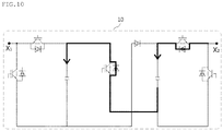
- Figs. 9 and 10 are diagrams showing the flows of fault current in the sub-module according to the present invention.
- the circuit unit 300 is configured such that the fault current flows into each of the energy storage units 110 and 210, thereby reducing or blocking the fault current.
- the sub-module of the present invention does not require the diode 9, unlike the conventional sub-module, while reducing or blocking fault current at a level equal or higher than that of the conventional sub-module. This means that the effects of the simplification of the configuration and the reduction in cost can be achieved.
- the auxiliary circuit unit when a plurality of sub-modules are configured, two half-bridge units are provided, an auxiliary circuit unit is disposed therebetween, and the auxiliary circuit unit is implemented using a single power semiconductor and a single diode, thereby reducing the number of diodes by one compared to the conventional sub-module while maintaining the same output and performance as the conventional sub-module. Due to this reduction in the number of diodes, the reduction in manufacturing cost can be achieved and the simplification of the configuration can be also achieved.
- the auxiliary circuit unit may be configured in various forms.
Description
- The present invention relates to a converter and, more particularly, to a converter in which a plurality of sub-modules, each including an energy storage unit and power semiconductors, is connected in series to each other, wherein each of the sub-modules is configured by adding a simple and inexpensive auxiliary circuit unit between two half-bridge units, and thus fault current is allowed to flow into the energy storage unit of each half-bridge unit, thereby blocking or reducing the fault current.
- In the case of a High Voltage Direct Current (HVDC) transmission converter, a power semiconductor that can be turn-on/turn-off controlled is used in order to perform conversion between alternating current (AC) voltage and direct current (DC) voltage. Since the withstanding voltage of the power semiconductor is limitative, a plurality of semiconductor modules having power semiconductor circuits must be connected in series in order to perform high voltage processing. In order to configure the power semiconductor circuits, various semiconductor modules may be connected to each other.
- As is well known, a well-known Modular Multilevel Converter (MMC) includes a plurality of sub-modules in which such power semiconductor circuits form two output terminals X1 and X2, and these plurality of sub-module is connected in series. Each of the sub-modules includes, for example, an energy storage unit and power semiconductors. The power semiconductors may be implemented using power semiconductor switches and freewheeling diodes, for example, IGBTs. This sub-module includes a so-called half-bridge or full-bridge circuit in which a plurality of power semiconductors is connected to each other. Furthermore, in the sub-modules of the MMC converter, one of the voltage of the energy storage units, zero voltage or the polarity-reversed voltage of the energy storage units appears at two output terminals.
- In
Fig. 1 , a well-known MMC converter is shown. In this converter, one ormore phase modules 1 are provided, and each of thephase modules 1 is configured such that a plurality ofsub-modules 10 is connected in series to each other. As load connection terminals, AC voltage-side terminals L1, L2 and L3 may be connected to a three-phase load, for example, a three-phase AC power system. - In
Fig. 2 , an example of the equivalent circuit of such asub-module 10 is shown. In the example ofFig. 2 , thesub-module 10 includes a single half-bridge unit 11. The half-bridge unit 11 includes anenergy storage unit 1 and a plurality ofpower semiconductors 6 connected in parallel to theenergy storage unit 1. Thepower semiconductors 6 may be configured usingpower semiconductor switches freewheeling diodes sub-module 10 ofFig. 2 is problematic in that thesub-module 10 is damaged by high fault current. - In order to mitigate the above problem, a conventional method in which an auxiliary circuit unit was added between two half-bridge units, as shown in
Fig. 3 , was presented. InFig. 3 , another example of the equivalent circuit of thesub-module 10 is shown. In thesub-module 10 shown in the example ofFig. 3 , two half-bridge units auxiliary circuit unit 14 is added therebetween. In this case, theauxiliary circuit unit 14 includes onepower semiconductor 7 and twodiodes energy storage units 1 and 1' of both half-bridge units Fig. 3 are shown inFigs. 4 and5 . -
Figs. 4 and5 are diagrams showing the flows of fault current in the conventional sub-module. InFig. 4 , fault current from a system (in the direction of X1->X2) flows into the firstenergy storage unit 1 through thefirst power semiconductor 6 of the first half-bridge unit 12, and, at the same time, flows into the second energy storage unit 1' through thediode 8 of theauxiliary circuit unit 14. Furthermore, inFig. 5 , fault current (in the direction of X2->X1) flows into the second energy storage unit 1' through the second power semiconductor 6' of the second half-bridge unit 13, and, at the same time, flows into the firstenergy storage unit 1 through thethird power semiconductor 7 of theauxiliary circuit unit 14. - Meanwhile, recently, as research into such auxiliary circuit units has been carried out, there has been a demand for a technology that is capable of simplifying the configuration of an auxiliary circuit unit and reducing the manufacturing cost thereof while implementing performance and efficiency equal to or higher than those of the conventional technology.
-
WO 2012/072168 A2 discloses a converter comprising a plurality of sub-modules connected in series to each other, wherein: each of the sub-modules comprises: a first half-bridge unit comprising a first energy storage unit, and a plurality of first power semiconductors connected in parallel to the first energy storage unit and connected in series to each other; a second half-bridge unit comprising a second energy storage unit, and a plurality of second power semiconductors connected in parallel to the second energy storage unit and connected in series to each other; and an auxiliary circuit unit connecting the first half-bridge unit and the second half-bridge unit; wherein the auxiliary circuit unit comprises a single third power semiconductor and a single diode. - A further device is known from Marquardt R: "Modular Multileavel Converter: An universal concept for HVDC-Networks and extended DC-Bus-applications", IEEE IPEC, 21 June 2010 (2010-06-21), pages 502-507, XP031729731.
- Accordingly, the present invention has been made in response to the above problems of the conventional technology and the technical demand, and an object of the present invention is to provide a converter in which each sub-module of the converter is configured using two half-bridge units and an auxiliary circuit unit disposed between the two half-bridge units and configured to be simpler and less inexpensive than that of the conventional technology, and thus fault current is allowed to flow into the energy storage unit of each half-bridge unit, thereby blocking or reducing the fault current.
- In order to accomplish the above object, the present invention provides a converter including a plurality of sub-modules connected in series to each other, wherein each of the sub-modules includes a first half-bridge unit including a first energy storage unit, and a plurality of first power semiconductors connected in parallel to the first energy storage unit and connected in series to each other; a second half-bridge unit including a second energy storage unit, and a plurality of second power semiconductors connected in parallel to the second energy storage unit and connected in series to each other; and an auxiliary circuit unit connecting the first half-bridge unit and the second half-bridge unit; wherein the auxiliary circuit unit includes a single third power semiconductor and a single diode.
- In the present invention, the (+) terminal of the first energy storage unit and the (-) terminal of the second energy storage unit may be connected through the third power semiconductor, and the (-) terminal of the first energy storage unit and a (+) terminal of the second energy storage unit may be connected through the diode.
- In the present invention, the emitter terminal of the third power semiconductor may be connected to the (-) terminal of any one of the first and second energy storage unit.
- In the present invention, when fault current flows into the sub-module, the fault current may be supplied to each energy storage unit of the first and second half-bridge units through any one of the third power semiconductor and diode of the auxiliary circuit unit.
- In the present invention, the fault current may be supplied to the energy storage unit through the diode of the auxiliary circuit unit when the fault current flows from a system to a DC side, and the fault current may be supplied to the energy storage unit through the third power semiconductor of the auxiliary circuit unit when the fault current flows from the DC side to the system.
- In the present invention, the third power semiconductor may be connected in parallel to the first energy storage unit, and the diode may be connected in series to the first energy storage unit.
- In the present invention, the (-) terminal of the first energy storage unit may be connected to an anode (+) terminal of the diode, and the cathode (-) terminal of the diode may be connected to the emitter terminal of the third power semiconductor.
- In the present invention, the third power semiconductor may be connected in parallel to the second energy storage unit, and the diode may be connected in series to the second energy storage unit.
- In the present invention, the (+) terminal of the second energy storage unit may be connected to the cathode (-) terminal of the diode, and the anode (+) terminal of the diode may be connected to the collector terminal of the third power semiconductor.
- The converter according to the present invention, which is configured as described above, can achieve the following effects.
- According to the present invention, in the implementation of a plurality of sub-modules applied to the converter, the present invention has the effects of simplifying the configuration thereof and reducing the implementation cost thereof compared to the conventional technology.
- Furthermore, according to the present invention, in the converter, each of the plurality of sub-modules is implemented using two half-bridge units and an auxiliary circuit unit disposed therebetween, and thus fault current is allowed to flow into the energy storage unit of each half-bridge unit, thereby blocking or reducing the fault current.
-
-
Fig. 1 is an equivalent circuit diagram showing a conventional well-known converter; -
Fig. 2 is a diagram of an exemplary configuration of the sub-module of the converter ofFig. 1 ; -
Fig. 3 is a diagram of another exemplary configuration of the sub-module of the converter ofFig. 1 ; -
Fig. 4 is a diagram showing the flows of fault current according to a conventional example; -
Fig. 5 is a diagram showing the flows of fault current according to another conventional example; -
Fig. 6 is a diagram showing the configuration of a sub-module of a converter according to an embodiment of the present invention; -
Fig. 7 is a diagram showing the configuration of a sub-module of a converter according to another embodiment of the present invention; -
Fig. 8 is a diagram showing the configuration of a sub-module of a converter according to still another embodiment of the present invention; -
Fig. 9 is a diagram showing the flows of fault current according to an example of the present invention; and -
Fig. 10 is a diagram showing the flows of fault current according to another example of the present invention. - Preferred embodiments of the present invention will be described in detail below with reference to the accompanying diagrams. In the following description of the present invention, if it is determined that detailed descriptions of related well-known functions or configurations unnecessarily make the gist of the present invention obscure, the detailed descriptions are omitted.
- The present invention provides a converter. In this converter, a plurality of sub-modules each including an energy storage unit and power semiconductors are connected in series to each other. Each of the sub-modules is designed to reduce or block fault current. This is described in detail below.
-
Fig. 6 is a diagram showing the configuration of a sub-module of a converter according to an embodiment of the present invention. - As shown in
Fig. 6 , each sub-module 10 of the converter according to the embodiment of the present invention includes a first half-bridge unit 100 and a second half-bridge unit 200, and anauxiliary circuit unit 300 is disposed between the first and second half-bridge units auxiliary circuit unit 300 functions to connect the first and second half-bridge units - The first half-
bridge unit 100 includes a firstenergy storage unit 110, and a plurality offirst power semiconductors 120 connected in parallel to the firstenergy storage unit 110 and connected in series to each other. The second half-bridge unit 200 includes a secondenergy storage unit 210, and a plurality ofsecond power semiconductors 220 connected in parallel to the secondenergy storage unit 210 and connected in series to each other. Although the number of first andsecond power semiconductor Fig. 6 , the present invention is not limited thereto. Thesepower semiconductors power semiconductors 120 of the first half-bridge unit 100, and a second output terminal X2 is connected to a neutral point between the twopower semiconductors 220 of the second half-bridge unit 200. - Furthermore, the
auxiliary circuit unit 300 includes a singlethird power semiconductor 310 and asingle diode 320. In this case, as shown in an embodiment ofFig. 6 , the (+) terminal of the firstenergy storage unit 110 of the first half-bridge unit 100 and the (-) terminal of the secondenergy storage unit 210 of the second half-bridge unit 200are connected to each other through the
third power semiconductor 310 of theauxiliary circuit unit 300, and the (-) terminal of the firstenergy storage unit 110 and the (+) terminal of the secondenergy storage unit 210 are connected to each other through thediode 320 of theauxiliary circuit unit 300. In this case, the emitter terminal of thethird power semiconductor 310 is connected to the (-) terminal of any one of the first and secondenergy storage units - In the sub-module 10 having the above configuration, when fault current flows from a system or fault current flows from a DC side, the fault current is allowed to flow into the first
energy storage unit 110 and the secondenergy storage unit 210 through any one of thethird power semiconductor 310 and diode 32 of theauxiliary circuit unit 300, thereby blocking or reducing the fault current. This flow of the fault current will be more specifically described in the following description. -
Fig. 7 is a diagram showing the configuration of a sub-module of a converter according to another embodiment of the present invention. - As shown in
Fig. 7 , each sub-module 10 of the converter according to this embodiment of the present invention also includes a first half-bridge unit 100 and a second half-bridge unit 200, and anauxiliary circuit unit 300 is disposed between the first and second half-bridge units Fig. 6 . However, some of the internal configuration of theauxiliary circuit unit 200 are different from those ofFig. 6 . - That is, the
auxiliary circuit unit 300 shown inFig. 7 includes a singlethird power semiconductor 310 and asingle diode 320, thethird power semiconductor 310 is connected in parallel to the firstenergy storage unit 110 of the first half-bridge unit 100, anddiode 320 is connected in series to the firstenergy storage unit 110. In this case, the (-) terminal of the firstenergy storage unit 110 and the anode (+) terminal of thediode 320 are connected to each other, and the cathode (-) terminal of thediode 320 and the emitter terminal of thethird power semiconductor 310 are connected to each other. - Also in the sub-module 10 having this configuration, when fault current flows from a system or fault current flows from a DC side, the fault current is allowed to flow into the first
energy storage unit 110 and the secondenergy storage unit 210 through any one of thethird power semiconductor 310 and diode 32 of theauxiliary circuit unit 300, thereby blocking or reducing the fault current. -
Fig. 8 is a diagram showing the configuration of a sub-module of a converter according to still another embodiment of the present invention. - As shown in
Fig. 8 , each sub-module 10 of the converter according to this embodiment of the present invention also includes a first half-bridge unit 100 and a second half-bridge unit 200, like those ofFigs. 6 and7 , and anauxiliary circuit unit 300 is disposed between the first and second half-bridge units auxiliary circuit unit 200 ofFig. 8 are different in its internal configuration from those ofFigs. 6 and7 . - That is, the
auxiliary circuit unit 300 shown inFig. 8 includes a singlethird power semiconductor 310 and asingle diode 320, thethird power semiconductor 310 is connected in parallel to the secondenergy storage unit 210 of the second half-bridge unit 200, and thediode 320 is connected in series to the secondenergy storage unit 210. In this case, the (+) terminal of the secondenergy storage unit 210 and the cathode (-) terminal of thediode 320 are connected to each other, and the anode (+) terminal of thediode 320 and the collector terminal of thethird power semiconductor 310 are connected to each other. - Also in the sub-module 10 having this configuration, when fault current flows from a system or fault current flows from a DC side, the fault current is allowed to flow into the first
energy storage unit 110 and the secondenergy storage unit 210 through any one of thethird power semiconductor 310 and diode 32 of theauxiliary circuit unit 300, thereby blocking or reducing the fault current. -
Figs. 9 and10 are diagrams showing the flows of fault current in the sub-module according to the present invention. - As shown in
Fig. 9 , when fault current flows from the system into the sub-module 10 (in the direction of X1->X2), the fault current flows into the firstenergy storage unit 110 through thefirst power semiconductor 120 of the first half-bridge unit 100, and, at the same time, the fault current flows into the secondenergy storage unit 210 through thediode 320 of theauxiliary circuit unit 300. - Furthermore, as shown in
Fig. 10 , when fault current flows into the sub-module 10 in a system direction (the direction of X2->X1), the fault current flows into the secondenergy storage unit 210 through thesecond power semiconductor 220 of the second half-bridge unit 200, and, at the same time, the fault current flows into the firstenergy storage unit 110 through thethird power semiconductor 310 of theauxiliary circuit unit 300. - As described above, comparing the flows of fault current in the sub-module according to the present invention auxiliary with the flows of fault current in the conventional sub-module shown in
Figs. 4 and5 , thecircuit unit 300 is configured such that the fault current flows into each of theenergy storage units diode 9, unlike the conventional sub-module, while reducing or blocking fault current at a level equal or higher than that of the conventional sub-module. This means that the effects of the simplification of the configuration and the reduction in cost can be achieved. - Accordingly, in the converter of the present invention, when a plurality of sub-modules are configured, two half-bridge units are provided, an auxiliary circuit unit is disposed therebetween, and the auxiliary circuit unit is implemented using a single power semiconductor and a single diode, thereby reducing the number of diodes by one compared to the conventional sub-module while maintaining the same output and performance as the conventional sub-module. Due to this reduction in the number of diodes, the reduction in manufacturing cost can be achieved and the simplification of the configuration can be also achieved. In the present invention, the auxiliary circuit unit may be configured in various forms.
- It is noted that although the present invention has been described in detail using the preferred embodiments, the present invention is not limited to the content of these embodiments. It will be apparent to those having ordinary knowledge in the technical field to which the present invention pertains that various modifications and improvements to the present invention, although these are not presented in the embodiments, can be made without departing from the range of the description of the attached claims, and all these modification and improvements fall within the technical range of the present invention. Therefore, the true range of the technical protection of the present invention should be defined based on the technical spirit of the attached claims.
Claims (4)
- A converter comprising a plurality of sub-modules (10) connected in series to each other, wherein:
each of the sub-modules (10) comprises:a first half-bridge unit (100) comprising a first energy storage unit (110), and a plurality of first power semiconductors (120) connected in parallel to the first energy storage unit (110) and connected in series to each other;a second half-bridge unit (200) comprising a second energy storage unit (210), and a plurality of second power semiconductors (220) connected in parallel to the second energy storage unit (210) and connected in series to each other; andan auxiliary circuit unit (300) connecting the first half-bridge unit (100) and the second half-bridge unit (200) ;wherein the auxiliary circuit unit (300) comprises a single third power semiconductor (310) and a single diode (320),wherein the third power semiconductor (310) is connected in parallel to the first (110) of the energy storage units (110, 210) only and the diode is connected in series to the first energy storage unit (110),wherein a collector terminal of the single third power semiconductor (310) is directly connected to a positive terminal of the first energy storage unit (110), an anode terminal of the single diode (320) is directly connected to a negative terminal of the first energy storage unit (110), and a common connection point of an emitter terminal of the single third power semiconductor (310) and a cathode terminal of the single diode (320) is directly connected to a negative terminal of the second energy storage unit (210) . - A converter comprising a plurality of sub-modules (10) connected in series to each other, wherein:
each of the sub-modules (10) comprises:a first half-bridge unit (100) comprising a first energy storage unit (110), and a plurality of first power semiconductors (120) connected in parallel to the first energy storage unit (110) and connected in series to each other;a second half-bridge unit (200) comprising a second energy storage unit (210), and a plurality of second power semiconductors (220) connected in parallel to the second energy storage unit (210) and connected in series to each other; andan auxiliary circuit unit (300) connecting the first half-bridge unit (100) and the second half-bridge unit (200) ;wherein the auxiliary circuit unit (300) comprises a single third power semiconductor (310) and a single diode (320),wherein the single third power semiconductor (310) is connected in parallel to the second (210) of the energy storage units (110, 210) only, and is further connected in series to the first energy storage unit (110), and the single diode (320) is connected in series to the second energy storage unit (210),wherein an emitter terminal of the single third power semiconductor (310) is directly connected to a negative terminal of the second energy storage unit (210), a cathode terminal of the single diode (320) is directly connected to a positive terminal of the second energy storage unit (210), and a common connection point of a collector terminal of the single third power semiconductor (310) and an anode terminal of the single diode (320) is directly connected to a positive terminal of the first energy storage unit (110). - The converter of claim 1 or 2, wherein when fault current flows into a sub-module (10) of the plurality of sub-modules (10), the fault current is supplied to each energy storage unit (110, 210) of the first (100) and second half-bridge units (200) through any one of the single third power semiconductor (310) and diode of the auxiliary circuit unit (300) .
- The converter of claim 3, wherein the fault current is supplied to the second energy storage unit (210) through the single third power semiconductor (310) of the auxiliary circuit unit (300) when the fault current flows in a first direction, and the fault current is supplied to the first energy storage unit (110) through the single diode (320) of the auxiliary circuit unit (300) when the fault current flows in an apposite direction to the first direction.
Applications Claiming Priority (2)
| Application Number | Priority Date | Filing Date | Title |
|---|---|---|---|
| KR1020120157390A KR101373170B1 (en) | 2012-12-28 | 2012-12-28 | Converter |
| PCT/KR2013/012342 WO2014104836A1 (en) | 2012-12-28 | 2013-12-27 | Converter |
Publications (3)
| Publication Number | Publication Date |
|---|---|
| EP2940852A1 EP2940852A1 (en) | 2015-11-04 |
| EP2940852A4 EP2940852A4 (en) | 2016-11-16 |
| EP2940852B1 true EP2940852B1 (en) | 2018-07-25 |
Family
ID=50648407
Family Applications (1)
| Application Number | Title | Priority Date | Filing Date |
|---|---|---|---|
| EP13867398.3A Active EP2940852B1 (en) | 2012-12-28 | 2013-12-27 | Converter |
Country Status (4)
| Country | Link |
|---|---|
| US (1) | US9590489B2 (en) |
| EP (1) | EP2940852B1 (en) |
| KR (1) | KR101373170B1 (en) |
| WO (1) | WO2014104836A1 (en) |
Families Citing this family (9)
| Publication number | Priority date | Publication date | Assignee | Title |
|---|---|---|---|---|
| CN104052026B (en) * | 2014-05-29 | 2016-05-25 | 华中科技大学 | For submodule topology and the application thereof of modularization multi-level converter |
| US9871437B2 (en) * | 2014-07-10 | 2018-01-16 | University-Industry Foundation(UIF) | Fault current reduction structure of multi-level converter and apparatus using the fault current reduction structure |
| DE102015105889A1 (en) * | 2015-04-17 | 2016-10-20 | Ge Energy Power Conversion Technology Limited | Switching module and converter with at least one switching module |
| CN104953793B (en) * | 2015-06-12 | 2018-09-11 | 中国科学院电工研究所 | A kind of clamp submodule topology |
| KR101943881B1 (en) * | 2016-12-26 | 2019-01-30 | 효성중공업 주식회사 | Mmc converter |
| KR101943885B1 (en) * | 2017-06-02 | 2019-01-30 | 효성중공업 주식회사 | MMC converter and submodule thereof |
| KR101943884B1 (en) * | 2017-06-02 | 2019-01-30 | 효성중공업 주식회사 | MMC converter and submodule thereof |
| CN107592010A (en) * | 2017-08-05 | 2018-01-16 | 天津大学 | Modular multilevel dynamic switching DC DC transformers |
| CN110943636B (en) * | 2019-11-25 | 2023-04-28 | 国网山东省电力公司潍坊供电公司 | Multi-level module for eliminating direct current short-circuit current |
Family Cites Families (16)
| Publication number | Priority date | Publication date | Assignee | Title |
|---|---|---|---|---|
| US4117364A (en) | 1976-05-14 | 1978-09-26 | Massachusetts Institute Of Technology | Voltage waveform synthesizer and a system that includes the same |
| GB9526674D0 (en) | 1995-12-29 | 1996-02-28 | Davy Process Techn Ltd | Reactor |
| US6198178B1 (en) | 1999-12-21 | 2001-03-06 | International Power Systems, Inc. | Step wave power converter |
| SE513846C2 (en) | 1999-03-29 | 2000-11-13 | Abb Ab | VSCconverter |
| EP1253706B1 (en) | 2001-04-25 | 2013-08-07 | ABB Schweiz AG | Power electronic circuit and process to transfer active power |
| DE10217889A1 (en) * | 2002-04-22 | 2003-11-13 | Siemens Ag | Power supply with a direct converter |
| ES2693612T3 (en) | 2007-03-13 | 2018-12-12 | Siemens Aktiengesellschaft | Procedure for limiting damage to a current converter that has power semiconductors in the event of a short circuit in the direct voltage intermediate circuit |
| DE102009057288B4 (en) * | 2009-12-01 | 2018-02-15 | Siemens Aktiengesellschaft | Inverters for high voltages |
| WO2012072168A2 (en) * | 2010-11-30 | 2012-06-07 | Technische Universität München | Novel multi-level converter topology with the possibility of dynamically connecting individual modules in series and in parallel |
| US8817504B2 (en) * | 2012-02-29 | 2014-08-26 | General Electric Company | Multilevel converter and topology method thereof |
| US9748848B2 (en) * | 2012-10-11 | 2017-08-29 | Siemens Aktiengesellschaft | Modular multilevel DC/DC converter for HVDC applications |
| KR101389579B1 (en) * | 2012-12-28 | 2014-04-29 | 주식회사 효성 | Power converter |
| EP2768133B1 (en) * | 2013-02-14 | 2015-11-04 | ABB Technology Ltd | Converter cell with reduced power losses, high voltage multilevel converter and associated method |
| US9461557B2 (en) * | 2013-03-22 | 2016-10-04 | Abb Ab | Bipolar double voltage cell and multilevel converter with such a cell |
| KR101512188B1 (en) * | 2014-02-11 | 2015-04-22 | 한국전기연구원 | A driving method of the modular multi-level converter and the apparatus thereof |
| CN104868748B (en) * | 2014-02-20 | 2017-12-22 | 南京南瑞继保电气有限公司 | A kind of current changer module unit, transverter, DC transmission system and control method |
-
2012
- 2012-12-28 KR KR1020120157390A patent/KR101373170B1/en active IP Right Grant
-
2013
- 2013-12-27 EP EP13867398.3A patent/EP2940852B1/en active Active
- 2013-12-27 WO PCT/KR2013/012342 patent/WO2014104836A1/en active Application Filing
- 2013-12-27 US US14/758,095 patent/US9590489B2/en active Active
Non-Patent Citations (1)
| Title |
|---|
| None * |
Also Published As
| Publication number | Publication date |
|---|---|
| EP2940852A4 (en) | 2016-11-16 |
| US9590489B2 (en) | 2017-03-07 |
| US20150357906A1 (en) | 2015-12-10 |
| KR101373170B1 (en) | 2014-03-12 |
| EP2940852A1 (en) | 2015-11-04 |
| WO2014104836A1 (en) | 2014-07-03 |
Similar Documents
| Publication | Publication Date | Title |
|---|---|---|
| EP2940852B1 (en) | Converter | |
| US10560019B2 (en) | Bipolar high-voltage network and method for operating a bipolar high-voltage network | |
| US9331595B2 (en) | Multi-level inverter | |
| US7411802B2 (en) | Method of converting a direct current voltage from a source of direct current voltage, more specifically from a photovoltaic source of direct current voltage, into a alternating current voltage | |
| JP5113078B2 (en) | Switchgear cell and converter circuit for switching multiple voltage levels | |
| US9337746B2 (en) | Multilevel inverter | |
| US20160141963A1 (en) | Modular multi-level dc-dc converter for hvdc applications | |
| US11451135B2 (en) | Multilevel port under-voltage protection circuit with flying capacitor | |
| US11139733B2 (en) | Modular multilevel converter sub-module having DC fault current blocking function and method of controlling the same | |
| CN108173442B (en) | Isolated modular multilevel converter based on high-frequency chain technology | |
| US8493760B2 (en) | Electric circuit for converting direct current into alternating current | |
| US10312825B2 (en) | Five-level half bridge inverter topology with high voltage utilization ratio | |
| EP2747268A1 (en) | Voltage source current controlled multilevel power converter | |
| TW201703417A (en) | Five-level converting device | |
| US20230114612A1 (en) | Inverter and Inverter Apparatus | |
| KR102261327B1 (en) | Inverter system | |
| US11038436B2 (en) | Inverter system | |
| EP3568904B1 (en) | Method and system for fault handling in a dc power transmission system | |
| JP2019110746A (en) | Power electronics module for charging stand, corresponding charging stand and power charging stand | |
| US9647529B2 (en) | Modular multi-stage inverter comprising surge arrester | |
| KR102261330B1 (en) | Inverter system | |
| CN110999054B (en) | Power module for converter and multilevel converter | |
| US20220385209A1 (en) | Power Conversion Device | |
| SE1300553A1 (en) | DC / DC converter with multiple ports |
Legal Events
| Date | Code | Title | Description |
|---|---|---|---|
| PUAI | Public reference made under article 153(3) epc to a published international application that has entered the european phase |
Free format text: ORIGINAL CODE: 0009012 |
|
| 17P | Request for examination filed |
Effective date: 20150722 |
|
| AK | Designated contracting states |
Kind code of ref document: A1 Designated state(s): AL AT BE BG CH CY CZ DE DK EE ES FI FR GB GR HR HU IE IS IT LI LT LU LV MC MK MT NL NO PL PT RO RS SE SI SK SM TR |
|
| AX | Request for extension of the european patent |
Extension state: BA ME |
|
| DAX | Request for extension of the european patent (deleted) | ||
| A4 | Supplementary search report drawn up and despatched |
Effective date: 20161013 |
|
| RIC1 | Information provided on ipc code assigned before grant |
Ipc: H02M 7/483 20070101AFI20161007BHEP |
|
| GRAP | Despatch of communication of intention to grant a patent |
Free format text: ORIGINAL CODE: EPIDOSNIGR1 |
|
| INTG | Intention to grant announced |
Effective date: 20180219 |
|
| GRAS | Grant fee paid |
Free format text: ORIGINAL CODE: EPIDOSNIGR3 |
|
| GRAA | (expected) grant |
Free format text: ORIGINAL CODE: 0009210 |
|
| AK | Designated contracting states |
Kind code of ref document: B1 Designated state(s): AL AT BE BG CH CY CZ DE DK EE ES FI FR GB GR HR HU IE IS IT LI LT LU LV MC MK MT NL NO PL PT RO RS SE SI SK SM TR |
|
| REG | Reference to a national code |
Ref country code: GB Ref legal event code: FG4D |
|
| REG | Reference to a national code |
Ref country code: CH Ref legal event code: EP |
|
| REG | Reference to a national code |
Ref country code: AT Ref legal event code: REF Ref document number: 1022838 Country of ref document: AT Kind code of ref document: T Effective date: 20180815 |
|
| REG | Reference to a national code |
Ref country code: IE Ref legal event code: FG4D |
|
| REG | Reference to a national code |
Ref country code: DE Ref legal event code: R096 Ref document number: 602013040985 Country of ref document: DE |
|
| REG | Reference to a national code |
Ref country code: DE Ref legal event code: R081 Ref document number: 602013040985 Country of ref document: DE Owner name: HYOSUNG HEAVY INDUSTRIES CORP., KR Free format text: FORMER OWNER: HYOSUNG CORP., SEOUL, KR Ref country code: DE Ref legal event code: R082 Ref document number: 602013040985 Country of ref document: DE Representative=s name: VIERING, JENTSCHURA & PARTNER MBB PATENT- UND , DE Ref country code: DE Ref legal event code: R081 Ref document number: 602013040985 Country of ref document: DE Owner name: HYOSUNG HEAVY INDUSTRIES CORP., SEOUL, KR Free format text: FORMER OWNER: HYOSUNG CORP., SEOUL, KR |
|
| REG | Reference to a national code |
Ref country code: GB Ref legal event code: 732E Free format text: REGISTERED BETWEEN 20181018 AND 20181024 |
|
| REG | Reference to a national code |
Ref country code: NL Ref legal event code: MP Effective date: 20180725 |
|
| REG | Reference to a national code |
Ref country code: NO Ref legal event code: T2 Effective date: 20180725 |
|
| REG | Reference to a national code |
Ref country code: LT Ref legal event code: MG4D |
|
| PG25 | Lapsed in a contracting state [announced via postgrant information from national office to epo] |
Ref country code: NL Free format text: LAPSE BECAUSE OF FAILURE TO SUBMIT A TRANSLATION OF THE DESCRIPTION OR TO PAY THE FEE WITHIN THE PRESCRIBED TIME-LIMIT Effective date: 20180725 |
|
| REG | Reference to a national code |
Ref country code: AT Ref legal event code: MK05 Ref document number: 1022838 Country of ref document: AT Kind code of ref document: T Effective date: 20180725 |
|
| PG25 | Lapsed in a contracting state [announced via postgrant information from national office to epo] |
Ref country code: LT Free format text: LAPSE BECAUSE OF FAILURE TO SUBMIT A TRANSLATION OF THE DESCRIPTION OR TO PAY THE FEE WITHIN THE PRESCRIBED TIME-LIMIT Effective date: 20180725 Ref country code: FI Free format text: LAPSE BECAUSE OF FAILURE TO SUBMIT A TRANSLATION OF THE DESCRIPTION OR TO PAY THE FEE WITHIN THE PRESCRIBED TIME-LIMIT Effective date: 20180725 Ref country code: RS Free format text: LAPSE BECAUSE OF FAILURE TO SUBMIT A TRANSLATION OF THE DESCRIPTION OR TO PAY THE FEE WITHIN THE PRESCRIBED TIME-LIMIT Effective date: 20180725 Ref country code: IS Free format text: LAPSE BECAUSE OF FAILURE TO SUBMIT A TRANSLATION OF THE DESCRIPTION OR TO PAY THE FEE WITHIN THE PRESCRIBED TIME-LIMIT Effective date: 20181125 Ref country code: AT Free format text: LAPSE BECAUSE OF FAILURE TO SUBMIT A TRANSLATION OF THE DESCRIPTION OR TO PAY THE FEE WITHIN THE PRESCRIBED TIME-LIMIT Effective date: 20180725 Ref country code: BG Free format text: LAPSE BECAUSE OF FAILURE TO SUBMIT A TRANSLATION OF THE DESCRIPTION OR TO PAY THE FEE WITHIN THE PRESCRIBED TIME-LIMIT Effective date: 20181025 Ref country code: GR Free format text: LAPSE BECAUSE OF FAILURE TO SUBMIT A TRANSLATION OF THE DESCRIPTION OR TO PAY THE FEE WITHIN THE PRESCRIBED TIME-LIMIT Effective date: 20181026 Ref country code: SE Free format text: LAPSE BECAUSE OF FAILURE TO SUBMIT A TRANSLATION OF THE DESCRIPTION OR TO PAY THE FEE WITHIN THE PRESCRIBED TIME-LIMIT Effective date: 20180725 Ref country code: PL Free format text: LAPSE BECAUSE OF FAILURE TO SUBMIT A TRANSLATION OF THE DESCRIPTION OR TO PAY THE FEE WITHIN THE PRESCRIBED TIME-LIMIT Effective date: 20180725 |
|
| PG25 | Lapsed in a contracting state [announced via postgrant information from national office to epo] |
Ref country code: AL Free format text: LAPSE BECAUSE OF FAILURE TO SUBMIT A TRANSLATION OF THE DESCRIPTION OR TO PAY THE FEE WITHIN THE PRESCRIBED TIME-LIMIT Effective date: 20180725 Ref country code: LV Free format text: LAPSE BECAUSE OF FAILURE TO SUBMIT A TRANSLATION OF THE DESCRIPTION OR TO PAY THE FEE WITHIN THE PRESCRIBED TIME-LIMIT Effective date: 20180725 Ref country code: HR Free format text: LAPSE BECAUSE OF FAILURE TO SUBMIT A TRANSLATION OF THE DESCRIPTION OR TO PAY THE FEE WITHIN THE PRESCRIBED TIME-LIMIT Effective date: 20180725 |
|
| REG | Reference to a national code |
Ref country code: DE Ref legal event code: R097 Ref document number: 602013040985 Country of ref document: DE |
|
| PG25 | Lapsed in a contracting state [announced via postgrant information from national office to epo] |
Ref country code: CZ Free format text: LAPSE BECAUSE OF FAILURE TO SUBMIT A TRANSLATION OF THE DESCRIPTION OR TO PAY THE FEE WITHIN THE PRESCRIBED TIME-LIMIT Effective date: 20180725 Ref country code: ES Free format text: LAPSE BECAUSE OF FAILURE TO SUBMIT A TRANSLATION OF THE DESCRIPTION OR TO PAY THE FEE WITHIN THE PRESCRIBED TIME-LIMIT Effective date: 20180725 Ref country code: EE Free format text: LAPSE BECAUSE OF FAILURE TO SUBMIT A TRANSLATION OF THE DESCRIPTION OR TO PAY THE FEE WITHIN THE PRESCRIBED TIME-LIMIT Effective date: 20180725 Ref country code: RO Free format text: LAPSE BECAUSE OF FAILURE TO SUBMIT A TRANSLATION OF THE DESCRIPTION OR TO PAY THE FEE WITHIN THE PRESCRIBED TIME-LIMIT Effective date: 20180725 Ref country code: IT Free format text: LAPSE BECAUSE OF FAILURE TO SUBMIT A TRANSLATION OF THE DESCRIPTION OR TO PAY THE FEE WITHIN THE PRESCRIBED TIME-LIMIT Effective date: 20180725 |
|
| PG25 | Lapsed in a contracting state [announced via postgrant information from national office to epo] |
Ref country code: DK Free format text: LAPSE BECAUSE OF FAILURE TO SUBMIT A TRANSLATION OF THE DESCRIPTION OR TO PAY THE FEE WITHIN THE PRESCRIBED TIME-LIMIT Effective date: 20180725 Ref country code: SM Free format text: LAPSE BECAUSE OF FAILURE TO SUBMIT A TRANSLATION OF THE DESCRIPTION OR TO PAY THE FEE WITHIN THE PRESCRIBED TIME-LIMIT Effective date: 20180725 Ref country code: SK Free format text: LAPSE BECAUSE OF FAILURE TO SUBMIT A TRANSLATION OF THE DESCRIPTION OR TO PAY THE FEE WITHIN THE PRESCRIBED TIME-LIMIT Effective date: 20180725 |
|
| PLBE | No opposition filed within time limit |
Free format text: ORIGINAL CODE: 0009261 |
|
| STAA | Information on the status of an ep patent application or granted ep patent |
Free format text: STATUS: NO OPPOSITION FILED WITHIN TIME LIMIT |
|
| 26N | No opposition filed |
Effective date: 20190426 |
|
| REG | Reference to a national code |
Ref country code: CH Ref legal event code: PL |
|
| PG25 | Lapsed in a contracting state [announced via postgrant information from national office to epo] |
Ref country code: MC Free format text: LAPSE BECAUSE OF FAILURE TO SUBMIT A TRANSLATION OF THE DESCRIPTION OR TO PAY THE FEE WITHIN THE PRESCRIBED TIME-LIMIT Effective date: 20180725 Ref country code: LU Free format text: LAPSE BECAUSE OF NON-PAYMENT OF DUE FEES Effective date: 20181227 Ref country code: SI Free format text: LAPSE BECAUSE OF FAILURE TO SUBMIT A TRANSLATION OF THE DESCRIPTION OR TO PAY THE FEE WITHIN THE PRESCRIBED TIME-LIMIT Effective date: 20180725 |
|
| REG | Reference to a national code |
Ref country code: IE Ref legal event code: MM4A |
|
| REG | Reference to a national code |
Ref country code: BE Ref legal event code: MM Effective date: 20181231 |
|
| PG25 | Lapsed in a contracting state [announced via postgrant information from national office to epo] |
Ref country code: IE Free format text: LAPSE BECAUSE OF NON-PAYMENT OF DUE FEES Effective date: 20181227 Ref country code: FR Free format text: LAPSE BECAUSE OF NON-PAYMENT OF DUE FEES Effective date: 20181231 |
|
| PG25 | Lapsed in a contracting state [announced via postgrant information from national office to epo] |
Ref country code: BE Free format text: LAPSE BECAUSE OF NON-PAYMENT OF DUE FEES Effective date: 20181231 |
|
| PG25 | Lapsed in a contracting state [announced via postgrant information from national office to epo] |
Ref country code: CH Free format text: LAPSE BECAUSE OF NON-PAYMENT OF DUE FEES Effective date: 20181231 Ref country code: LI Free format text: LAPSE BECAUSE OF NON-PAYMENT OF DUE FEES Effective date: 20181231 |
|
| PG25 | Lapsed in a contracting state [announced via postgrant information from national office to epo] |
Ref country code: MT Free format text: LAPSE BECAUSE OF NON-PAYMENT OF DUE FEES Effective date: 20181227 |
|
| PG25 | Lapsed in a contracting state [announced via postgrant information from national office to epo] |
Ref country code: TR Free format text: LAPSE BECAUSE OF FAILURE TO SUBMIT A TRANSLATION OF THE DESCRIPTION OR TO PAY THE FEE WITHIN THE PRESCRIBED TIME-LIMIT Effective date: 20180725 |
|
| PG25 | Lapsed in a contracting state [announced via postgrant information from national office to epo] |
Ref country code: PT Free format text: LAPSE BECAUSE OF FAILURE TO SUBMIT A TRANSLATION OF THE DESCRIPTION OR TO PAY THE FEE WITHIN THE PRESCRIBED TIME-LIMIT Effective date: 20180725 |
|
| PG25 | Lapsed in a contracting state [announced via postgrant information from national office to epo] |
Ref country code: HU Free format text: LAPSE BECAUSE OF FAILURE TO SUBMIT A TRANSLATION OF THE DESCRIPTION OR TO PAY THE FEE WITHIN THE PRESCRIBED TIME-LIMIT; INVALID AB INITIO Effective date: 20131227 Ref country code: MK Free format text: LAPSE BECAUSE OF NON-PAYMENT OF DUE FEES Effective date: 20180725 Ref country code: CY Free format text: LAPSE BECAUSE OF FAILURE TO SUBMIT A TRANSLATION OF THE DESCRIPTION OR TO PAY THE FEE WITHIN THE PRESCRIBED TIME-LIMIT Effective date: 20180725 |
|
| PGFP | Annual fee paid to national office [announced via postgrant information from national office to epo] |
Ref country code: NO Payment date: 20200721 Year of fee payment: 8 |
|
| PGFP | Annual fee paid to national office [announced via postgrant information from national office to epo] |
Ref country code: DE Payment date: 20200721 Year of fee payment: 8 |
|
| REG | Reference to a national code |
Ref country code: DE Ref legal event code: R119 Ref document number: 602013040985 Country of ref document: DE |
|
| REG | Reference to a national code |
Ref country code: NO Ref legal event code: MMEP |
|
| PG25 | Lapsed in a contracting state [announced via postgrant information from national office to epo] |
Ref country code: NO Free format text: LAPSE BECAUSE OF NON-PAYMENT OF DUE FEES Effective date: 20211231 Ref country code: DE Free format text: LAPSE BECAUSE OF NON-PAYMENT OF DUE FEES Effective date: 20220701 |
|
| PGFP | Annual fee paid to national office [announced via postgrant information from national office to epo] |
Ref country code: GB Payment date: 20231006 Year of fee payment: 11 |