EP2899870A2 - A nestable single cell structure for use in a power conversion system - Google Patents
A nestable single cell structure for use in a power conversion system Download PDFInfo
- Publication number
- EP2899870A2 EP2899870A2 EP15152266.1A EP15152266A EP2899870A2 EP 2899870 A2 EP2899870 A2 EP 2899870A2 EP 15152266 A EP15152266 A EP 15152266A EP 2899870 A2 EP2899870 A2 EP 2899870A2
- Authority
- EP
- European Patent Office
- Prior art keywords
- switch
- cell
- output
- power
- switch elements
- Prior art date
- Legal status (The legal status is an assumption and is not a legal conclusion. Google has not performed a legal analysis and makes no representation as to the accuracy of the status listed.)
- Granted
Links
- 238000006243 chemical reaction Methods 0.000 title description 21
- 239000003990 capacitor Substances 0.000 claims abstract description 83
- 238000000034 method Methods 0.000 claims description 29
- 238000010586 diagram Methods 0.000 description 25
- 238000004891 communication Methods 0.000 description 14
- 230000008878 coupling Effects 0.000 description 13
- 238000010168 coupling process Methods 0.000 description 13
- 238000005859 coupling reaction Methods 0.000 description 13
- 238000013459 approach Methods 0.000 description 11
- 230000006870 function Effects 0.000 description 10
- 239000004065 semiconductor Substances 0.000 description 10
- 230000001276 controlling effect Effects 0.000 description 9
- 238000004590 computer program Methods 0.000 description 8
- 230000008569 process Effects 0.000 description 6
- 230000001105 regulatory effect Effects 0.000 description 6
- 230000009471 action Effects 0.000 description 5
- 230000002457 bidirectional effect Effects 0.000 description 5
- 238000007667 floating Methods 0.000 description 4
- 230000003287 optical effect Effects 0.000 description 4
- 230000008646 thermal stress Effects 0.000 description 4
- 230000007704 transition Effects 0.000 description 4
- 230000003213 activating effect Effects 0.000 description 3
- 238000012986 modification Methods 0.000 description 3
- 230000004048 modification Effects 0.000 description 3
- 238000012545 processing Methods 0.000 description 3
- 230000008901 benefit Effects 0.000 description 2
- 238000001514 detection method Methods 0.000 description 2
- 238000004146 energy storage Methods 0.000 description 2
- 238000004519 manufacturing process Methods 0.000 description 2
- 230000007935 neutral effect Effects 0.000 description 2
- 230000035882 stress Effects 0.000 description 2
- 238000004804 winding Methods 0.000 description 2
- 230000004913 activation Effects 0.000 description 1
- 230000006978 adaptation Effects 0.000 description 1
- 230000006399 behavior Effects 0.000 description 1
- 239000006227 byproduct Substances 0.000 description 1
- 238000004364 calculation method Methods 0.000 description 1
- 230000003915 cell function Effects 0.000 description 1
- 230000001413 cellular effect Effects 0.000 description 1
- 230000009849 deactivation Effects 0.000 description 1
- 230000007812 deficiency Effects 0.000 description 1
- 230000001419 dependent effect Effects 0.000 description 1
- 238000005516 engineering process Methods 0.000 description 1
- 239000000835 fiber Substances 0.000 description 1
- 230000005669 field effect Effects 0.000 description 1
- 238000001914 filtration Methods 0.000 description 1
- 230000016507 interphase Effects 0.000 description 1
- 238000002955 isolation Methods 0.000 description 1
- 229910044991 metal oxide Inorganic materials 0.000 description 1
- 150000004706 metal oxides Chemical class 0.000 description 1
- 230000010363 phase shift Effects 0.000 description 1
- 230000009467 reduction Effects 0.000 description 1
- 238000009877 rendering Methods 0.000 description 1
- 230000003362 replicative effect Effects 0.000 description 1
- 230000004044 response Effects 0.000 description 1
- 238000012552 review Methods 0.000 description 1
- 230000000630 rising effect Effects 0.000 description 1
- 238000004088 simulation Methods 0.000 description 1
Images


Classifications
-
- H—ELECTRICITY
- H02—GENERATION; CONVERSION OR DISTRIBUTION OF ELECTRIC POWER
- H02M—APPARATUS FOR CONVERSION BETWEEN AC AND AC, BETWEEN AC AND DC, OR BETWEEN DC AND DC, AND FOR USE WITH MAINS OR SIMILAR POWER SUPPLY SYSTEMS; CONVERSION OF DC OR AC INPUT POWER INTO SURGE OUTPUT POWER; CONTROL OR REGULATION THEREOF
- H02M7/00—Conversion of ac power input into dc power output; Conversion of dc power input into ac power output
- H02M7/42—Conversion of dc power input into ac power output without possibility of reversal
- H02M7/44—Conversion of dc power input into ac power output without possibility of reversal by static converters
- H02M7/48—Conversion of dc power input into ac power output without possibility of reversal by static converters using discharge tubes with control electrode or semiconductor devices with control electrode
- H02M7/483—Converters with outputs that each can have more than two voltages levels
- H02M7/4837—Flying capacitor converters
-
- H—ELECTRICITY
- H02—GENERATION; CONVERSION OR DISTRIBUTION OF ELECTRIC POWER
- H02M—APPARATUS FOR CONVERSION BETWEEN AC AND AC, BETWEEN AC AND DC, OR BETWEEN DC AND DC, AND FOR USE WITH MAINS OR SIMILAR POWER SUPPLY SYSTEMS; CONVERSION OF DC OR AC INPUT POWER INTO SURGE OUTPUT POWER; CONTROL OR REGULATION THEREOF
- H02M7/00—Conversion of ac power input into dc power output; Conversion of dc power input into ac power output
- H02M7/42—Conversion of dc power input into ac power output without possibility of reversal
- H02M7/44—Conversion of dc power input into ac power output without possibility of reversal by static converters
- H02M7/48—Conversion of dc power input into ac power output without possibility of reversal by static converters using discharge tubes with control electrode or semiconductor devices with control electrode
- H02M7/483—Converters with outputs that each can have more than two voltages levels
- H02M7/49—Combination of the output voltage waveforms of a plurality of converters
-
- H—ELECTRICITY
- H02—GENERATION; CONVERSION OR DISTRIBUTION OF ELECTRIC POWER
- H02M—APPARATUS FOR CONVERSION BETWEEN AC AND AC, BETWEEN AC AND DC, OR BETWEEN DC AND DC, AND FOR USE WITH MAINS OR SIMILAR POWER SUPPLY SYSTEMS; CONVERSION OF DC OR AC INPUT POWER INTO SURGE OUTPUT POWER; CONTROL OR REGULATION THEREOF
- H02M1/00—Details of apparatus for conversion
- H02M1/08—Circuits specially adapted for the generation of control voltages for semiconductor devices incorporated in static converters
-
- H—ELECTRICITY
- H02—GENERATION; CONVERSION OR DISTRIBUTION OF ELECTRIC POWER
- H02K—DYNAMO-ELECTRIC MACHINES
- H02K47/00—Dynamo-electric converters
-
- H—ELECTRICITY
- H02—GENERATION; CONVERSION OR DISTRIBUTION OF ELECTRIC POWER
- H02M—APPARATUS FOR CONVERSION BETWEEN AC AND AC, BETWEEN AC AND DC, OR BETWEEN DC AND DC, AND FOR USE WITH MAINS OR SIMILAR POWER SUPPLY SYSTEMS; CONVERSION OF DC OR AC INPUT POWER INTO SURGE OUTPUT POWER; CONTROL OR REGULATION THEREOF
- H02M7/00—Conversion of ac power input into dc power output; Conversion of dc power input into ac power output
- H02M7/42—Conversion of dc power input into ac power output without possibility of reversal
- H02M7/44—Conversion of dc power input into ac power output without possibility of reversal by static converters
- H02M7/48—Conversion of dc power input into ac power output without possibility of reversal by static converters using discharge tubes with control electrode or semiconductor devices with control electrode
- H02M7/483—Converters with outputs that each can have more than two voltages levels
- H02M7/487—Neutral point clamped inverters
-
- H—ELECTRICITY
- H02—GENERATION; CONVERSION OR DISTRIBUTION OF ELECTRIC POWER
- H02M—APPARATUS FOR CONVERSION BETWEEN AC AND AC, BETWEEN AC AND DC, OR BETWEEN DC AND DC, AND FOR USE WITH MAINS OR SIMILAR POWER SUPPLY SYSTEMS; CONVERSION OF DC OR AC INPUT POWER INTO SURGE OUTPUT POWER; CONTROL OR REGULATION THEREOF
- H02M1/00—Details of apparatus for conversion
- H02M1/0003—Details of control, feedback or regulation circuits
-
- H—ELECTRICITY
- H02—GENERATION; CONVERSION OR DISTRIBUTION OF ELECTRIC POWER
- H02M—APPARATUS FOR CONVERSION BETWEEN AC AND AC, BETWEEN AC AND DC, OR BETWEEN DC AND DC, AND FOR USE WITH MAINS OR SIMILAR POWER SUPPLY SYSTEMS; CONVERSION OF DC OR AC INPUT POWER INTO SURGE OUTPUT POWER; CONTROL OR REGULATION THEREOF
- H02M1/00—Details of apparatus for conversion
- H02M1/0095—Hybrid converter topologies, e.g. NPC mixed with flying capacitor, thyristor converter mixed with MMC or charge pump mixed with buck
-
- H—ELECTRICITY
- H02—GENERATION; CONVERSION OR DISTRIBUTION OF ELECTRIC POWER
- H02M—APPARATUS FOR CONVERSION BETWEEN AC AND AC, BETWEEN AC AND DC, OR BETWEEN DC AND DC, AND FOR USE WITH MAINS OR SIMILAR POWER SUPPLY SYSTEMS; CONVERSION OF DC OR AC INPUT POWER INTO SURGE OUTPUT POWER; CONTROL OR REGULATION THEREOF
- H02M1/00—Details of apparatus for conversion
- H02M1/32—Means for protecting converters other than automatic disconnection
- H02M1/325—Means for protecting converters other than automatic disconnection with means for allowing continuous operation despite a fault, i.e. fault tolerant converters
Definitions
- the present invention relates generally to multi-level topologies for power conversion devices.
- the present invention relates to more effective multi- level topologies in high power applications.
- power quality is a significant factor when interfacing with the electric grid and electric machines. Maintaining high power quality can be important to avoid issues, such as electromagnetic interference (EMI) pollution, flicker, and shortened life of electric machines due to high current harmonics and dv/dt stresses. Power converters play an important role in this process.
- EMI electromagnetic interference
- Multi-level converter topologies more easily achieve high power quality, high density at higher efficiency.
- Interfacing with AC electric source and/or load, such as utility grid and electric machines multi-level converters emulate alternating current (AC) output waveforms by providing multiple voltage levels at the output of the converter. Consequently, switching frequency can be reduced due to lowered output harmonics as result of the multi-level output.
- AC alternating current
- NPC neutral point clamped
- a first approach includes multiple converters, generally connected in parallel (or shunt), and coupled with interphase reactors or transformers. This first approach is controlled with interleaved pulse width modulation (PWM) and produces multiple output voltage levels. Drawbacks of this approach include circulating current among the parallel coupled converters, ultimately leading to higher losses, lower semiconductor utilization, and increased control complexity.
- PWM pulse width modulation
- a second approach includes multiple single-phase H-bridges (either two-level or three-level H-bridges) connected in series (or cascaded), where each of those single- phase H-bridges are connected to isolated DC links. Due to galvanic isolation provided by a multi-winding transformer, the H-bridges can be coupled together directly with cascaded connection to produce multi-level output voltages correspondingly. Multi- winding transformers, however, are complex and bulky. Also, this approach is difficult and costly to be tailored for four-quadrant operation.
- capacitors and power semiconductors tend to have higher density and lower cost than that of magnetic components. Therefore, in comparison to coupling multiple converters with magnetic components, coupling multiple converters with (flying) capacitors provides better power density and efficiency at a lower cost.
- Modular multi-level converters are yet an additional and widely used capacitor based topology.
- a number of modular H-bridges are cascaded directly to provide multiple output voltage levels, each one having its own floating DC link capacitors.
- the voltage levels of these DC links are tightly regulated, using the load current among multi-phases of the cascaded bridge legs.
- the size of the DC-link capacitors is inversely proportional to the fundamental frequency of the corresponding AC terminal. This solution, therefore, is not optimal for low and variable frequency applications, such as motor drives, due to fairly large floating DC link capacitors.
- a better approach than the conventional approaches described above includes coupling multiple converters together through flying capacitors to provide multiple output voltage levels. Voltages across the flying capacitors are regulated every switching cycle. As such, the capacitor size is inversely proportional to switching frequency, instead of the fundamental frequency of the AC source or load. Since the switching frequency is typically more than 30-50 times higher than fundamental frequency, floating or flying capacitor size can be effectively reduced. A further increase of power density, and a reduction in cost, can be thus achieved.
- a power conversion module includes a capacitor module having a plurality of connecting terminals and a plurality of switch elements. Each switch element has at least one switch terminal coupled to a corresponding connecting terminal, wherein the switch elements are configured for mutually exclusive operation via a control device.
- Embodiments of the present invention provide efficient multi-level voltage outputs with at least one nested neutral point piloted (NPP) cell. Additionally, systems constructed in accordance with the embodiments include at least one relatively simple three-level NPP structure, along with a unique control system. These NPP structures are scalable to higher voltage applications requiring outputs of more than three levels by simply duplicating the structure in a nested manner.
- NPP neutral point piloted
- Flying capacitors within the nested NPP structures, are actively controlled and balanced within one or more switching cycles to maintain their voltage levels. In this manner, the size of the capacitors is inversely proportional to switching frequency, not the fundamental frequency of the AC terminal. Using this approach, increased power quality and power density can be achieved.
- the embodiments include other advantages, such as fault redundancy with series devices, flying capacitor balancing, and more robust/faster short circuit and device overvoltage detection. Some embodiments use redundant switching states to achieve additional control features, such as regulation of the flying capacitor voltages and/or balance of thermal stress of power semiconductor switches in different switch positions.
- a cell can include three switch elements formed of a combination unidirectional and bi-directional switching devices. DC link capacitors in these cells are provided, along with six or more connection terminals to facilitate nested arrangements having an inner cell and outer cell.
- Each switch element can be formed of multiple power semiconductor devices connected in series.
- the series connection can extend the voltage rating of each switch element and enhance reliability by reducing the voltage stress of each power semiconductor device.
- Fault tolerant operation is provided by simply bypassing faulty semiconductor devices.
- a byproduct of the disclosed control techniques is faster detection of faults, such as de-saturation and overvoltage of power semiconductor switches.
- the nested structure of the NPP modules can be implemented in a hybrid arrangement, where at least one of the outer cells is a nested NPP cell, while the inner cell may have different topology and/or output levels, such as a 3-level NPC cell or a 2-level cell.
- a hybrid arrangement may also include the inner and outer cells with different types and/or sizes of power switches.
- the nested structure of the NPP cell can be implemented in a multi-phase power conversion system.
- a multi-phase (e.g. three-phase) converter with nested NPP cells, for example, can share one DC link to provide three-phase DC-AC, AC-DC, or DC-DC conversion.
- a converter module comprises at least three switch units, at least three input-cascading terminals, and at least three output-cascading terminals, wherein the three input-cascading terminals are coupled to three output-cascading terminals of another converter module or coupled to corresponding terminals of a DC link, respectively, and the three output-cascading terminals are coupled to the three input-cascading terminals of another converter module, respectively, or tied together, such that a multi-level converter device having a nested structure is formed, wherein the three switch units are controlled in a manner to perform switching actions independently from one another, and wherein each of the different output voltages provided from the three output-cascading terminals is exclusively associated with at least one turned-on status of the three switch units.
- the converter module can be a converter module that is placed at the outermost of the multi-level converter device, the three input-cascading terminals of the outermost converter module can be coupled to a first terminal, a second terminal, and a DC middle terminal of the DC link, respectively, the three output-cascading terminals of the outermost converter module can be coupled to the three input-cascading terminals of another converter module, wherein the at least three switch units comprise a first switch unit, a second switch unit, and a third switch unit, wherein a first output-cascading terminal of the outermost converter module provides a first level output voltage when the first switch unit is turned on and the second and third switch units are turned off, wherein a second output-cascading terminal of the outermost converter module provides a second level output voltage when the second switch unit is turned on and the first and third switch units are turned off, and wherein a third output-cascading terminal of the outermost converter module provides a third level output voltage when the third switch unit is turned on and the
- the converter module can be a converter module that is placed at the innermost of the multi-level converter device, the three input-cascading terminals of the innermost converter module can be coupled to the three output-cascading terminals of another converter module, respectively, and the three output-cascading terminals of the innermost converter module can be commonly coupled to an output terminal of the multi-level converter device, wherein the at least three switch units comprise a first switch unit, a second switch unit, and a third switch unit, wherein a first output-cascading terminal of the innermost converter module provides a first level output voltage when the first switch unit is turned on and the second and third switch units are turned off, wherein a second output-cascading terminal of the innermost converter module provides a second level output voltage when the second switch unit is turned on and the first and third switch units are turned off, and wherein a third output-cascading terminal of the innermost converter module provides a third level output voltage when the third switch unit is turned on and the first and second switch units are turned off
- the converter module can comprise a longitudinal arm and a transverse arm substantially perpendicular to the longitudinal arm, at least two of the three switch units are placed at the longitudinal arm, and at least one of the three switch units is placed at the transverse arm.
- the switch unit placed at the transverse arm can comprise a bi-directionally controllable switch.
- the at least three switch units can comprise a first switch unit, a second switch unit, and a third switch unit, the third switch unit can comprise a first sub-switch and a second sub-switch, the first and second sub-switches can be uni-directionally controllable switches, and the controllable directions of the first and second sub-switches can be opposite.
- One of the control signals applied to the first and second sub-switches can have a lead time period or a lag time period, at one or more signal transition edges, relative to the control signals applied to the first switch unit or the second switch unit, and the other of the control signals applied to the first and second sub-switches can have a lag time period or a lead time period, at one or more signal transition edges, relative to the control signals applied to the first switch unit or the second switch unit.
- a converter device comprises a first converter module, and a second converter module, wherein each of the first and second converter modules comprises at least three switch units, at least three input-cascading terminals, and at least three output-cascading terminals, wherein the three input-cascading terminals of the first converter module are coupled to the three output-cascading terminals of the second converter module, respectively, thereby the converter device is constructed to have a nested structure, wherein the three switch units of the first converter module are controlled to perform switching actions independently from one another, and each of the turned-on status of the three switch units of the first converter module is exclusively corresponding to each of the three output voltages provided at the three output-cascading terminals of the first converter module, wherein the three switch units of the second converter module are controlled to perform switching actions independently from one another, and each of the turned-on status of the three switch units of the second converter module is exclusively corresponding to each of the three output voltages provided at the three output-cascading terminals of the second converter
- the three output-cascading terminals of the first converter module can be commonly coupled to the output terminal of the converter device.
- Each of the first and second converter modules can comprise a first switch unit, a second switch unit, and a third switch unit, and wherein at least the third switch unit can comprise a bi-directionally controllable switch.
- Each of the first and second converter modules can comprise a first switch unit, a second switch unit, and a third switch unit, and the third switch unit can comprise a first sub-switch and a second sub-switch, the first and second sub-switches can comprise uni-directionally controllable switch, and the controllable directions of the first and second sub-switches can be opposite.
- One of the control signals applied to the first and second sub-switches can have a lead time period or a lag time period, at one or more signal transition edges, relative to the control signals applied to the first switch unit or the second switch unit, and the other of the control signals applied to the first and second sub-switches can have a lag time period or a lead time period, at one or more signal transition edges, relative to the control signals applied to the first switch unit or the second switch unit.
- the converter device can further comprise a first flying capacitor, and a second flying capacitor coupled in series with the first flying capacitor. Voltages of the first flying capacitor and the second flying capacitor can be substantially balanced in one or more switching control cycles by selectively using output redundant states of the converter device.
- the first converter module can have substantially the same structure as the second converter module.
- the first converter module can be configured to provide output voltages having 2n 1 +1 levels and the second converter module can be configured to provide output voltages having 2n 2 +1 levels, where n 1 and n 2 are equal to or larger than one, and n 1 is equal to n 2 .
- the first converter module can have different structure than the second converter module.
- the first converter module can be configured to provide output voltages having 2n 1 +1 levels and the second converter module is configured to provide output voltages having 2n 2 +1 levels, where n 1 and n 2 are equal to or larger than one, and n 1 is different than n 2 .
- the converter device can comprise a longitudinal arm comprising at least one first switch unit and at least one second switch unit, and a transverse arm comprising at least one third switch unit, wherein the at least one first switch unit comprises N switch devices connected in series, the at least one second switch unit comprises M switch devices connected in series, the at least one third switch unit comprises K switch devices connected in series, and N, M, and K are larger than two.
- Each of two switch devices can be arranged with a respective snubber circuit, and the snubber circuit can be configured to ensure the at least two switch devices substantially share the same voltage during the process of the switch devices being switched on or off.
- a power conversion system for performing power conversion and providing electrical power to a load comprises a first converter for converting an input electrical power to a DC electrical power, and a second converter coupled to the first converter, the second converter converting the DC electrical power to an output electrical power and providing the output electrical power to the load, wherein at least one of the first and second converters comprises a first converter module, and a second converter module, wherein each of the first and second converter modules comprises at least three switch units, at least three input-cascading terminals, and at least three output-cascading terminals, wherein the three input-cascading terminals of the first converter module are coupled to the three output-cascading terminals of the second converter module, respectively, thereby the first converter or the second converter is constructed to have a nested structure, wherein the three switch units of the first converter module are controlled to perform switching actions independently, and wherein the three switch units of the second converter module are controlled to perform switching actions independently.
- the input electrical power can comprise an alternating current (AC) electrical power or a DC electrical power
- the second electrical power can comprise an AC electrical power or a DC electrical power.
- the three output-cascading terminals of the first converter module can be commonly coupled to the output terminal of the first converter or the second converter.
- Each of the turned-on status of the three switch units of the first converter module can exclusively correspond to each of the three output voltages provided at the three output-cascading terminals of the first converter module
- each of the turned-on status of the three switch units of the second converter module can exclusively correspond to each of the three output voltages provided at the three output-cascading terminals of the second converter module.
- the first converter can comprise a fully-controllable rectifying device or a non-fully-controllable rectifying device.
- circuit circuitry
- controller may include either a single component or a plurality of components, which are either active and/or passive components and may be optionally connected or otherwise coupled together to provide the described function.
- multi-level power conversion is achieved in a manner that provides higher power quality and density than conventional approaches at lower costs.
- a multi-level (e.g., three levels) NPP nested cell topology is provided to achieve the multiple output voltage levels.
- the nested cell topology is created by replicating individual cell structures, wrapping one cell around the other, forming an inner cell nested within an outer cell.
- switches devices, DC link capacitors, and other internal components can be configured to operate in a cascading manner to produce the required multiple output levels.
- the controller can be configured to control operation of the switch elements - activating (turning on) and deactivating (turning off) power switches within the switch elements, one at a time. Each time a power switch is activated, an output voltage level is expressed on one of the cells. Activating and deactivating the power switches enables precise control of the voltage levels output from the converter.
- FIG. 1A is a block diagram illustration of an exemplary basic 3-level cell 200 (e.g., NPP) configured for operation within one of the converters in an exemplary power conversion system.
- NPP basic 3-level cell 200
- FIG. 1A provides basic operational principles of NPP cells, in accordance with the embodiments.
- the 3-level NPP cell 200 includes switch elements 205, 228, and 232, which are controllable via a control device 140.
- the control device 140 controls operation of the NPP cell 200 via control signals 106.
- the control device 140 can be coupled to the NPP cell 200 through wireless, optical, or other similar communication links.
- Flying capacitors 261 and 263 form a capacitor module (e.g., DC link 226).
- the NPP cell 200 is nestable, or connectable, in a cascading arrangement with other cells with 2 or 3 connecting terminals, such as identical NPP cells.
- embodiments of the present invention are not limited to three switch elements nor to two flying capacitors.
- the switch element 228 includes connecting terminals 225 (having an interior orientation with respect to the cell 200) and 235 (e.g., exterior orientation with respect to the cell 200 and the direction of the element 228) at respective ends.
- the switch element 232 includes connecting terminals 229 (e.g., interior) and 241 (e.g., exterior) at respective ends.
- the switch element 205 includes connecting terminals 227 (interior) and 239 (exterior) at respective ends.
- the connecting terminal 239 is formed via the connection of the flying capacitors 261 and 263. One such connection is along the path formed by the serial connection of the flying capacitors 261 and 263.
- the other terminal of the flying capacitor 261 is coupled to the connecting terminals 235.
- the other terminal of the flying capacitor 263 is coupled to the connecting terminal 241.
- Control of the cell NPP 200 is achieved through manipulation of the switch elements 205, 228, and 232 in response to the control signals 106.
- the switching states of the switch elements 205, 228, and 232 occur mutually exclusively. That is, when one switch element within a cell is activated (ON), the other switch elements within that cell are deactivated (OFF), with substantially zero overlap between the various switching states. This mutually exclusive switching facilitates the efficient production of output voltages different levels.
- the switch element 228 when the switch element 228 is ON, the switch elements 205, and 232 are OFF, and the first output-cascading terminal 225 producers a first level output voltage of Vp.
- the switch element 232 When the switch element 232 is ON, the switch elements 205 and 228 are OFF, and the output-cascading terminal 229 produces a second level output voltage Vn.
- the switch element 205 when the switch element 205 is ON, the switch elements 228 and 232 are OFF, and the output-cascading terminal 227 provides a third level output voltage of Vmid, wherein the output levels are different from one another. More specifically, each of the different level output voltages (Vp, Vn, and Vmid) is exclusively associated with a respective ON switch element. This control process is explained in much greater detail below. In this manner, the NPP cell 200 represents a 3-level NPP cell topology.
- each of the switch elements 205, 228, and 232 can each be implemented as a power switch, each being controllable to permit bidirectional current flow.
- Switch elements 228 and 232 can block unidirectional voltage, while switch element 205 can block bidirectional voltage.
- one or more of the switch elements 228, and 232 can be implemented as two or more unidirectional power switches connected in series.
- Switch element 205 can be implemented with two or more unidirectional power switches connected in series in reverse polarity.
- multiple low-voltage devices connected in series generally provide a higher total voltage withstanding capability suitable for the application needs.
- the number of power switches within each switch element is an economic factor considered in the production cost and capacity of an individual converter.
- the present invention is not limited to switch elements that include only one or two power switches.
- FIG. 1B is a graphical illustration of an exemplary timing diagram 190 of timing signals generated to control the inner cell 200, depicted in FIG. 4 below.
- FIG. IB for example, at a time instance to power switch 205 is activated (ON state), going from “0" to “1” and power switch 228 is deactivated (OFF state), goes from “1” to “0.”
- the power switch 205 is deactivated, going from “1” to "0,” and a power switch 232 is activated, going from “0” to “1.”
- Activation and deactivation are controlled via drive signals (discussed in greater detail below) that can be generated by a single control device, such as the control device 140.
- Embodiments of the present invention can also produce a floating state in which all power switches are off, or disconnected from all other connecting terminals.
- FIG. 2A is a detailed block diagram illustration of an implementation of the inner cell 200 depicted in FIG. 1A .
- FIG. 2A also depicts gate drivers associated with the switch elements 228, 232, and 205.
- the multiple power switches in the inner cell 200 are also controlled to perform switching operations in a mutually exclusive manner.
- the switch element 228 is configured to be switched on/off according to drive signals 309 provided from a gate driver 301.
- the switch element 232 is configured to be switched on/off according to drive signals 315 provided from a gate driver 307.
- the power switch 234 (also referred to as sub-switch) is configured to be switched on/off according to switching drive signals 311 provided from a third gate driver 303.
- the power switch 236 (also referred to as second sub-switch) is configured to be switched on/off according to switching drive signals 313 provided from a gate driver 305.
- the drive signals 311 and 313 supplied to the power switches 234 and 236 operate synchronously.
- a first a drive signal 309 has a falling edge which indicates that the switch element 228 (S1) is changing from the ON state to the OFF state.
- t 0-y0 where "y 0 -y 7 " are finite time quanta occurring before or after time instant "t.” For example, t 0-y0 occurs prior to to, in which a first portion of the switch element 205 (S2) (e.g., power switch 236) is activated via a second drive signal 313.
- the switch element 205 is still controlled in an OFF state.
- the switch element 205 is controlled in an ON state only when both sub-switches 234 and 236 are turned on.
- a second portion e.g., the power switch 234
- the switch element 205 is turned on via a third drive signal 311.
- the switch element 205 formally changes to the ON state.
- the first portion of the switch element 205 (S2) (power switch 236) is deactivated during an OFF state via the second drive signal 313.
- a fourth drive signal 315 turns the switch element 232 (S4) to an ON state.
- the second portion of the switch element 205 (S3) (power switch 234) is formally turned to an OFF state via the third drive signal 311.
- time quanta y 0 - y7 can all be different values. The process described above is repeated for remaining states t 2 -t 3 . In this manner, the rising and falling edges of 228, 205, and 232 are substantially non-overlapping.
- FIG. 2C is a block diagram illustration of a power switch 228 of FIG. 2A in accordance with the embodiments.
- the switch element 228 can be configured to include any type of the power switches (internal to switch elements).
- the switch elements 238, 228, 232, 242 can be configured to precisely match the configuration of the switch element 228.
- the switch element 228 includes a power switch 316, a power switch 318, and an n-th power switch 322, where n is equal to or larger than two.
- the power switches 316 and 318 are connected in parallel with respective anti-parallel diodes 324, and 326.
- the n-th power switch 322 is connected in parallel with an n-th anti-parallel diode 328.
- each power switch can be integrated with its corresponding anti-parallel diode to form a single switch.
- each of the switches is applied with a portion of the DC voltage.
- low nominal voltage switches can be used to replace a single power switch 312, which has a high nominal voltage.
- the single power switch 312 is also integrated with an anti-parallel diode 314. Additionally, a higher number of power switches provides a greater level of redundancy.
- power switches described in the embodiments can be formed of metal oxide semiconductor field effect transistor (MOSFET), insulated gate bipolar transistor (IGBT), and integrated gate commutated thyristor (IGCT), to name a few.
- MOSFET metal oxide semiconductor field effect transistor
- IGBT insulated gate bipolar transistor
- IGCT integrated gate commutated thyristor
- FIG. 3 is a block diagram illustration of the outer cell 201 discussed above, according to the embodiments.
- FIG. 3 also depicts gate drivers associated with power switches within each of the switch elements 238, 242, and 271.
- the multiple devices in the outer cell 201 are controlled to perform switching operations in a mutually exclusive manner.
- the switch element 238 is configured to be switched on/off according to switching drive signals 325 provided from a gate driver 317.
- the switch element 242 is configured to be switched on/off according to switching drive signals 327 provided from a gate driver 319.
- the power switch 244, within the switch element 271, is configured to be switched on/off according to switching drive signals 329 provided from a gate driver 321.
- the power switch 246 is configured to be switched on/off according to drive signals 331 provided from a gate driver 323.
- the switching drive signals 329 and 331 operate synchronously and are generated from a single controller. To ensure the proper commutation of the switch elements 238 or 242, and to ensure dead time in order to avoid short-circuits of the flying capacitors, the switching instants of the drive signals 329 and 331 are adjusted. For example, the drive signals 329 and 331 may be adjusted accordingly in a manner to advance switching or delay switching of the sub-switches 246 and/or 244 in switch element 271 in a substantially small time quanta relative to the drive signals supplied to the switch element 238 or 242.
- FIG. 4 is a more detailed block diagram of one of the phase legs 220 of FIG. 1A .
- the first phase leg 220 is formed of a nested structure including the outer cell 201 wrapped around the inner cell 200.
- the components, structure and operation behavior within the inner cell 200 and the outer cell 201 are virtually identical. This technique enables the expansion of the 3-level topology of a basic NPP cell to achieve outputs having five levels (as in the case of the first phase leg 220), or seven, nine, eleven, or more levels.
- nested structures can be hybrid, for example, having a 2-level cell or 3-level NPC cell being wrapped within the 3-level NPP cell.
- Many other hybrid nested structures are possible and are within the spirit and scope of the present invention.
- the outer cell 201 includes capacitors 212 and 214.
- the capacitors 212 and 214 form a DC link 210.
- the capacitors 212 and 214 need not be configured to form a DC link.
- the capacitors 212 and 214 are essentially identical to the capacitors 261 and 263 of the inner cell 200 as "flying" capacitors.
- the power switches 238, 242, 244, and 246 of the outer cell 201 are essentially equivalent or identical to the power switches 228, 232, 234, and 236 of the inner cell 200.
- the switch element 205 is a bi-directional switch which conducts bidirectional current and blocks bidirectional voltage. It can be implemented as two reversely coupled unidirectional power switches 234 and 236. However, the present invention is not limited to this particular power switch implementation.
- the power switches 234 and 236 are controllable via the control device 140 to allow electrical currents having opposite directions to flow therethrough.
- the switch elements 228 and 232 can conduct bidirectional current and block unidirectional voltage.
- One of the terminals 235 of the switch element 228 is coupled to a terminal of the capacitor module 226, or more specifically, to a terminal of the flying capacitor 261. This coupling permits the terminal 235 to function as a first input-cascading terminal.
- the other terminal 225 of the switch element 228 functions as a first output- cascading terminal and is able to be coupled to the output terminal 260.
- One terminal of the switch element 232 is coupled to another terminal of the capacitor module 226, more specifically to one terminal of the flying capacitor 263, permitting the terminal 241 to function as a second input-cascading terminal.
- the connecting terminal 229 functions as a second output-cascading terminal and is also able to be coupled to the output terminal 260.
- a terminal 239 of the switch element 205 is coupled to a connection point 239 of the DC link 226 and functions as a third input-cascading terminal.
- Another terminal 227 of the switch element 205 functions as a third output-cascading terminal and is also couplable to the output terminal 260.
- the input-cascading terminals 235, 239, and 241 can be respectively coupled to three output-cascading terminals of another NPP cell (e.g., the cell 201).
- the cell 200 is the inner cell
- the cell 201 is the outer cell, as noted earlier.
- the output-cascading terminals 225, 227, and 229 can be respectively coupled to three input-cascading terminals of another cell.
- the cell 200 functions as the outer cell and the other cell functions as the inner cell.
- the cell 201 could similarly function as an inner cell. Nesting NPP cells in cascading arrangements allows expansion of the number of achievable voltage output levels.
- a voltage is output therefrom.
- the switch element 228 (oriented in the same direction as the switch element 232) is activated, the terminals 235 and 225 connect together.
- the switch element 205 is activated, the terminals 239 and 227 connect together.
- the switch element 232 is activated, the terminals 229 and 241 connect together.
- cell control is achieved by activating and deactivating the switch elements one at a time.
- components within the inner cell 200 have an S-level designation
- components within the outer cell 201 have a T-level designation. Transitioning from one switching state to the next switching state, within respective S and T levels, is accomplished through coordination of the control signals 106 provided to each cell from the control device 140.
- each of the control signals 106 can include multiple control signals sent simultaneously to gate drivers within individual power switches of each switch element, for all power switches in a particular level. For example, one signal to power switches within the switch element 228 (S1), another signal to 232 (S4), and a third signal to switch element 205, including power switches 236/234 (S2/S3). Also, one signal to 238 (T1), another signal to 242 (T4), and a third signal to 244/246 (T2/T3).
- This coordinated signal control ensures that no more than one switch element in the S-level inner cell 200 is ON at a given time. Similarly, no more than one switch element in the T-level outer cell 201 is ON at a given time
- the nested cell structures within the phase leg 220 combined with use of the control device 140, produces multi-level output voltages of higher power quality and power density.
- the structure of these nested cells can be replicated, with each cell producing a predetermined number of outputs, to expand the number of voltage output levels.
- the inner cell 200 can be configured and controlled to provide an output voltage having three levels.
- the outer cell 201 can be configured and controlled to provide an output voltage having three levels. Output voltage level of the phase leg with nested cells would be 2*cell number +1, when both inner and outer cells are 3-level cells.
- the inner cell 200 and the outer cell 201 provide 5-level output voltages. More specifically, and by way of example only, and not limitation, capacitors and switch elements within each of the cells 200 and 201 are structured to have six connecting terminals. The connecting terminals of one cell structure connect with corresponding connecting terminals of the other cell structure.
- the outer NPP cell 201 includes switch elements 238, 242, and 271.
- the switch element 238 has a connecting terminal 237 (e.g., interior) at one end and a connecting terminal 211 (e.g., exterior) at its other end.
- the switch element 242 is oriented in the same direction as the switch element 238.
- the switch element 242 has a connecting terminal 221 (interior) at one end and 215 (exterior) at its other end.
- the switch element 271 includes power switches 244 and 246 that are reversely coupled in series.
- the switch element 271 has a connecting terminal 219 (interior) at one end.
- a connecting terminal (exterior) of the switch element 271 is coupled to a connecting terminal 216 defined between the capacitors 212 and 214 of the capacitor module 210.
- the ends of the capacitor 212 are coupled to the two connecting terminals 211 and 216 respectively.
- two ends of the second capacitor 214 are coupled to the two connecting terminals 216 and 215, respectively.
- nested NPP cell structures are formed by coupling the connecting terminals 237 and 235 together, coupling the connecting terminals 219 and 239 together, and coupling the connecting terminals 241 and 221, together.
- similar connections can be made to form a higher level converter topology by connecting more than three six-terminal converter modules.
- the connecting terminals 225, 227, 229 (i.e., interior terminals) of the inner cell 200, are connected to the AC port 260 for receiving or providing AC voltage.
- connecting terminal 211 is coupled to the DC port 202 through the first DC line 206.
- the connecting terminal 215 is coupled to the DC port 204 through the DC line 208. In this manner, the connecting terminals 211 and 215 are configured to receive or provide DC voltages.
- FIG. 5A is an illustration of an exemplary state machine voltage level diagram for two nested cells structure (inner cell 200 and outer cell 201).
- a first digit within each oval 560 represents a state of the outer cell 201.
- a second digit within the oval 560 represents a state of the inner cell 200.
- two equally valid states can occur to produce the same output voltage levels of 1 and -1, respectively, as illustrated in greater detail below with reference to FIGs. 5B and 5C .
- FIG. 5B is a tabular illustration of exemplary switching states for controlling the inner and outer cell structures 200 and 201 of FIGs. 5A and 5B configured in the phase leg 220 of FIG. 4 .
- the first phase leg 220 can be controlled to provide an output voltage having five different voltage levels 501.
- the voltage levels 501 are produced by selectively controlling the outer cell 201 switches (T-level switches) via switching states 502 and the inner cell 200 switches (S-level switches) via switching states 504.
- FIG. 5C is a graphical illustration including exemplary timing signals 512 and 514 and the resultant output voltage waveform 511.
- timing signals 512 are representative of switching states 502 (see FIG. 5B ) for the components ( FIG. 3 ) within the outer cell 201.
- timing signals 514 are representative of switching states 504 for components ( FIG. 5B ) within the inner cell 200.
- the sequential application of the timing signals 512 and 514 to the outer and inner cells 201 and 200 produces the output voltage having multiple levels and a selectable pattern. More specifically, the pattern of the output voltage 511 can resemble the sinusoidal pattern.
- the waveform 511 is produced as a multi-level output of the first phase leg 220 of the multi-phase converter 700 (or 122), depicted in FIG. 5C .
- Other non- sinusoidal waveform patterns are achievable and are within the spirit and scope of the present invention.
- the timing signals 512 are applied via the respective control signals 325, 327, 329, and 331, as described above.
- the timing signals 514 are applied via the respective control signals 309, 315, 311, and 313.
- the control signals, shown in FIGs. 5A and 5B can be sub-signals of the control signals 106, generated by the single control device 140.
- the control signals, shown in FIGs. 5A and 5B can be generated by multiple control devices.
- FIG. 5D is an illustration of an output voltage waveform 550 of the multi- phase converter in accordance with the embodiments. As shown in FIG. 5D , through the use of a converter having a nested cell structure and multiple phase legs, one phase leg of the converter can provide an output voltage having five or more levels in the form of substantial resemblance of desired alternate current waveform.
- flying capacitor voltage is maintained using redundant switching states.
- redundant switching states means that the same commanded level output may be provided by supplying switching signals having different combinations of switching states to the plurality of the power switches within the converter.
- Use of redundant switching states enables the pulse pattern of the individual pulse signals to be selected such that additional control objectives are achieved in addition to the desired output voltage waveforms.
- Those additional control objectives may include (a) regulation of flying capacitor voltage to a pre-determined value; and (b) balance of thermal stress of power switches in different switch positions.
- the output voltage of the nested cell structures is dependent upon the degree to which the voltage of the flying capacitors, such as the voltages cross flying capacitors 261/263 can be regulated to a pre-determined value.
- this regulation is achieved by actively controlling the current flowing through the flying capacitors through use of redundant switching states to charge and discharge the flying capacitor.
- FIG. 6A is an illustration of a first stage current flow path through a generic power converter phase leg 600, similar to the phase leg 220, of FIG. 4 , in accordance with another embodiment.
- FIG. 6B is an illustration of a second stage flow path through the generic power converter phase leg 600 of FIG. 6A .
- the final voltage output of a nested cell structure is the sum of the output from the outer three-level cell 201 and the inner three-level cell 200. That is, the final voltage output is the sum of the states of the two three-level NPP cells.
- Use of redundant switching states leverages the internal structure of the nested cells to achieve additional control and operation objectives, such as regulation of flying capacitor voltage and/or balance of thermal stress on power switches.
- the output from the outer cell 201 and the inner cell 200 can be “1” and “0,” respectively.
- the output can be "0" and "1,” producing an identical output voltage level.
- the current paths going to the corresponding flying capacitors would be opposite, causing one to charge, the other to discharge the flying capacitor 602.
- flying capacitor 602 is a capacitor through which a need exists for regulating operational characteristics therein, such as voltage.
- a first current path 604 depicts current flowing into the flying capacitor 602 and to an output 606. That is, in FIG. 6A , when an output voltage level of "1" is required at the output port 606, either the first current path 604 or a second current path 608 can be selected. Due to the switching states redundancy for operating the plurality of switch elements, either of the first or second current paths 604 and 608 (see FIG. 6B ) can be formed such that the flying capacitor 602 can be charged and/or discharged for regulation of its voltage.
- flying capacitor voltage information signals received by a controller 140' can indicate that the flying capacitor 602 is in an over- voltage condition or having a voltage greater than a pre-determined voltage level.
- the controller is configured to generate the individual pulse signals having a first combination of switching states, depicted in FIG. 6B , to allow the flying capacitor 602 to be discharged.
- the flying capacitor voltage information signals received by the controller could indicate that the flying capacitor 602 is in an under-voltage condition or having a voltage less than a pre-determined value.
- the pulse pattern generator is configured to generate the individual pulse signals having a second combination of switching states, as depicted in FIG. 6A , to allow the flying capacitor 602 to be charged. Consequently, the voltages at the flying capacitor 602 and the flying capacitor 610 can be dynamically regulated in every switching cycle.
- FIG. 7 is an exemplary block diagram illustration of a multiphase converter 700 formed by three separate phase legs 220, 250, and 280, in accordance with the embodiments.
- the phase leg 220 includes the single 3-level NPP cell 200 of FIG. 1A configured as an inner cell wrapped within an outer cell 201.
- Each of the phase legs 220, 250, and 280 is a single phase (e.g., 120° phase shift from each other) of a multiphase converter.
- FIG. 7 is discussed within the context of the converter 700. Greater details of nested cell structures were provided in the discussion above, particularly in the discussion of FIG. 4 above.
- each of the phase legs 220, 250, 280 is coupled between first and second DC lines 206 and 208 for receiving a DC voltage from a DC link 210 and providing an output voltage at corresponding output ports 260, 265, and 285.
- first and second DC lines 206 and 208 for receiving a DC voltage from a DC link 210 and providing an output voltage at corresponding output ports 260, 265, and 285.
- the phase legs 220, 250, and 280 provide corresponding first, second, and third phase AC voltages through output ports 260, 265, and 285, respectively.
- the first, second, and third phase AC voltages can be offset from one another by 120 degrees.
- the output ports 260, 265, and 285 can be alternatively configured as AC input ports to receive input AC voltages.
- first and second ports 202 and 204 can be configured as DC output ports to output DC voltages.
- those ports can be configured and connected accordingly in a similar fashion.
- FIG. 8 is an illustration of an exemplary 7-level nested NPP structure 800 in accordance with an alternative embodiment of the present invention. That is, the NPP structure (e.g., phase leg) 800 is capable of producing a 7-level output voltage.
- the NPP structure 800 in accordance with the NPP cell structures described above, includes the cells 200 and 201, described above. However, the structure 800 also includes a third cell - an exterior cell 203. Thus, the structure 800 includes three basic 3-level NPP cells in a nested arrangement.
- FIG. 9 is a block diagram illustration of an exemplary power conversion system 900 in which embodiments of the present invention can be practiced.
- the system 900 includes a nested NPP topology.
- the system 900 is a multi-level conversion system for achieving higher power quality and power density.
- the system 900 includes a power converter module 120 coupled to the control device 140.
- the exemplary power converter module 120 includes a first converter 122, a DC link/energy storage device 124, and a second converter 700.
- the first converter 122 converts a first AC power 102 from a first power device, such as a power source 110 (e.g., power grid) into DC power 123 (e.g., DC voltage).
- the converters 122 and 700 can include at least one basic 3-level NPP cell configured in a nested topology as discussed above, with reference to FIGs. 1A- 2B .
- a DC-link component within the device 124 can include one or more capacitors for filtering the DC voltage 123 output from the first converter 122 to supply a filtered DC voltage to the second converter 700.
- the second converter 700 converts the filtered DC voltage into a second AC voltage 104 (discussed in greater detail below).
- the second AC voltage 104 is output to a second power device, such as a power load 130 (e.g., an AC electric motor).
- the power conversion system 900 includes at least one 3-level NPP cell configured in a nested structure that provides more efficient multi-level power conversion for high power and, as well as for low and variable frequency applications.
- fixed-frequency electric power 102 e.g., 50 or 60 hertz AC
- variable-frequency electrical power 104 is supplied to the power load 130 (e.g., such as a motor).
- the power conversion system 900 can also include an energy storage component within the device 124, for storing the DC power provided from the first converter 122.
- FIG. 10 is a block diagram illustration 1000 of a control device 140' and a nested cell structure 220 constructed to implement the redundant switching state technique noted above.
- the system of FIG. 10 is configured to balance fly capacitor voltages by actively regulating the current flowing through the flying capacitors 261/263 of the capacitor module 226 through use of redundant switching states.
- control device 140' is similar to the control device 140 of FIGs. 1A and 9 .
- the control device 140' includes additional functionality for implementing the redundant states process discussed above.
- the control device 140' includes a high-order modulator 1002 configured to generate initial multi-level pulse signals 1003 by one or more modulation methods.
- the initial multi-level pulse signals 1003 are not directly transmitted for driving the nested phase leg 220. Instead, the initial multi-level pulse signals 1003 are used for generating individual pulse signals which in tum are used for driving a plurality of switch elements of the phase leg 220.
- the phase leg 220 can provide an output voltage and/or current having a waveform corresponding to the waveform of the initial multi-level pulse signals 1003.
- the high-order modulator 1002 can be configured to generate the initial multi-level pulse signals 1003 having five, seven, nine, eleven or more levels, corresponding to the output of the phase leg 220.
- the modulator 1002 is configured to generate the initial multi-level pulse signals 1003 by a multi-carrier modulation method such as, for example, a level-shifted pulse width modulation (LSPWM) method.
- a multi-carrier modulation method such as, for example, a level-shifted pulse width modulation (LSPWM) method.
- LSPWM level-shifted pulse width modulation
- the high-order modulator 1002 may be configured to generate the initial multi-level pulse signals 1003 using other modulation methods well known in the art.
- the modulator 1002 can receive a command signal 106' provided from a command signal generator 1004.
- the command signal 106' may include a voltage command signal having a waveform corresponding to that of a desired voltage.
- the voltage command signal 106' can have a sine waveform corresponding to a desired AC output voltage of the nested cell 220.
- the command signal 106' can also include a frequency command signal indicative of a desired output frequency.
- the high-order modulator 1002 can also receive multiple carrier signals 1008 provided from a carrier signal generator 1006.
- the carrier signal generator 1006 can generate multiple carrier signals, each carrier signal having a specific waveform shape (e.g., triangular, sawtooth, etc.).
- the carrier signals 1008 are shifted apart from each other to define a linear modulation range for the command signal 106'.
- voltages (V fc212 , V fc214 , V fc261 , and V fc263 ) of flying capacitors 261/263 can be directly obtained in real-time using one or more voltage sensors (not shown) in association with the flying capacitors. These real-time voltages are provided to the controller 140' via voltage information signals 1010 and 1012. In other embodiments, the flying capacitor voltages (V fc212 , V fc214 , V fc261 , and V fc263 ,) can be indirectly obtained through calculation or prediction.
- the pulse generator 1000 provides first and second level control signals control signals 1014 and 1016, respectively, to control operation of the nested cells 200 and 201 to synthesize the desired output voltage, while achieving additional control objectives, such as regulation of voltages cross flying capacitors (V fc212 , V fc214 , V fc261 , and V fc263 ), and/or balance thermal stress of power switches.
- the redundant switching states technique discussed above can be applied. For example, due to the switching states redundancy for operating the power switches within the inner cell 200 and the outer cell 201, a plurality of current paths can be formed These current paths allow the current to pass through selected circuit switches such that the flying capacitor 261/263 can be charged and/or discharged to maintain their voltages at pre-determined levels. This operation can occur within the operational principles of the S-level and T-level switching devices discussed above, for example, with respect to FIGs. 5A and 5B .
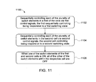
- FIG. 11 is a flow chart of an exemplary method 1100 of practicing an embodiment of the present invention.
- the method 1100 is provided for controlling an output of a power conversion system including two or more cells.
- Each of the two or more cells contains a plurality of switch elements, wherein at least one of the cells is a 3-level NPP cell.
- Method 1100 includes a first block 1102 that comprises sequentially controlling each of the plurality of switch elements in a first of the cells via first control signals, the step of sequentially controlling being responsive to a first switching state.
- Method 1100 further includes a second block 1104 comprising sequentially controlling each of the plurality of switch elements in the second cell via second control signals, the second cell controlling being responsive to a second switching state.
- the method 1100 further includes a block 1106, when one of the switch elements of the first or second cells is ON, all of the other of the switch elements within the respective cell are OFF.
- FIG. 12 is a block diagram illustration of an exemplary computer system 1200 upon which aspects of the present invention can be implemented.
- the computer system 1200 includes one or more processors, such as processor 1204.
- Processor 1204 may be a general purpose processor, such as a central processing unit (CPU) or a special purpose processor, such as a graphics processor unit (GPU).
- the processor 1204 is connected to a communication infrastructure 1206 (e.g., a communications bus, cross-over bar, or network).
- a communication infrastructure 1206 e.g., a communications bus, cross-over bar, or network.
- Computer system 1200 can include a graphics processing system 1202 which performs physics simulation and graphics processing tasks for rendering images to an associated display 1230.
- the computer system 1200 also includes a main memory 1208, preferably random access memory (RAM), and may also include a secondary memory 1210.
- main memory 1208, preferably random access memory (RAM) preferably random access memory (RAM)
- the secondary memory 1210 may include, for example, a hard disk drive 1212 and/or a removable storage drive 1214, representing a floppy disk drive, a magnetic tape drive, an optical disk drive, etc.
- the removable storage drive 1214 reads from and/or writes to a removable storage unit 1218.
- Removable storage unit 1218 represents a universal serial bus (USB) drive, flash drive, magnetic tape, optical disk, etc. which is read by and written to by removable storage drive 1214.
- USB universal serial bus
- the removable storage unit 1218 includes a computer usable storage medium having stored therein computer software and/or data.
- secondary memory 1210 may include other similar devices for allowing computer programs or other instructions to be loaded into computer system 1200.
- Such devices may include, for example, a removable storage unit 1222 and an interface 1220. Examples of such may include a program cartridge and cartridge interface, a removable memory chip (such as an erasable programmable read only memory (EPROM), or programmable read only memory (PROM)) and associated socket, and other removable storage units 1222 and interfaces 1220, which allow software and data to be transferred from the removable storage unit 1222 to computer system 1200.
- EPROM erasable programmable read only memory
- PROM programmable read only memory
- Computer system 1200 may also include a communications interface 1224.
- Communications interface 1224 allows software and data to be transferred between computer system 1200 and external devices.
- Examples of communications interface 1224 may include a modem, a network interface (such as an Ethernet card), a communications port, a personal computer memory card International Association (PCMCIA) slot and card, etc.
- PCMCIA personal computer memory card International Association
- Signal 1228 Software and data transferred via communications interface 1224 are in the form of signals 1228 which may be electronic, electromagnetic, optical, or other signals capable of being received by communications interface 1224. These signals 1228 are provided to communications interface 1224 via a communications path (e.g., channel) 1226.
- This channel 1226 carries signals 1228 and may be implemented using wire or cable, fiber optics, a telephone line, a cellular link, an radio frequency (RF) link and other communications channels.
- RF radio frequency
- computer program medium and “computer usable medium” are used to generally refer to media such as removable storage drive 1214, a hard disk installed in hard disk drive 1212, and signals 1228. These computer program products provide software to computer system 1200.
- Computer programs are stored in main memory 1208 and/or secondary memory 1210. Computer programs may also be received via communications interface 1224. Such computer programs, when executed, enable the computer system 1200 to perform features of the present invention, as discussed herein. Accordingly, such computer programs represent controllers of the computer system 1200.
- the software may be stored in a computer program product and loaded into computer system 1200 using removable storage drive 1214, hard drive 1212 or communications interface 1224.
- the control logic when executed by the processor 1204, causes the processor 1204 to perform the functions of the invention as described herein.
Abstract
Description
- The present invention relates generally to multi-level topologies for power conversion devices. In particular, the present invention relates to more effective multi- level topologies in high power applications.
- In power electronics, power quality, power density, and efficiency are among the most significant considerations when optimizing the conversion of power from one form to another. For example, power quality is a significant factor when interfacing with the electric grid and electric machines. Maintaining high power quality can be important to avoid issues, such as electromagnetic interference (EMI) pollution, flicker, and shortened life of electric machines due to high current harmonics and dv/dt stresses. Power converters play an important role in this process.
- There are generally two methods to achieve high power quality and density in power electronics: increasing switching frequency and multi-level topology. Increasing the switching frequency has limitation, especially for high power and/or medium voltage converters, due to higher losses of power semiconductors associated with higher switching frequency and intrinsic limit of switching speed for high voltage and high power semiconductor devices. Thus, for high voltage and high power applications, multi-level topology is a more effective approach than increasing switching frequency.
- Multi-level converter topologies more easily achieve high power quality, high density at higher efficiency. Interfacing with AC electric source and/or load, such as utility grid and electric machines, multi-level converters emulate alternating current (AC) output waveforms by providing multiple voltage levels at the output of the converter. Consequently, switching frequency can be reduced due to lowered output harmonics as result of the multi-level output. Several conventional multi-level topologies and control solutions are widely used in the industry.
- One conventional multi-level topology is a three-level neutral point clamped (NPC) topology, which has been the industry's workhorse for over a decade, especially for output voltage below 3.3 kV. However, expanding NPC technology beyond three- levels, in order to achieve higher power quality or for higher voltage applications, represents a significantly increased complexity, thus impractical for wide industry use.
- In order to achieve higher than three multi-level output, one has to find ways to couple multiple converters. There are fundamentally two ways for coupling multiple converters - (a) coupling through magnetic components, or (b) coupling through (flying) capacitors.
- There are two approaches (i.e., topologies) for coupling multiple converters through magnetic components to realize multi-level converters. A first approach includes multiple converters, generally connected in parallel (or shunt), and coupled with interphase reactors or transformers. This first approach is controlled with interleaved pulse width modulation (PWM) and produces multiple output voltage levels. Drawbacks of this approach include circulating current among the parallel coupled converters, ultimately leading to higher losses, lower semiconductor utilization, and increased control complexity.
- A second approach includes multiple single-phase H-bridges (either two-level or three-level H-bridges) connected in series (or cascaded), where each of those single- phase H-bridges are connected to isolated DC links. Due to galvanic isolation provided by a multi-winding transformer, the H-bridges can be coupled together directly with cascaded connection to produce multi-level output voltages correspondingly. Multi- winding transformers, however, are complex and bulky. Also, this approach is difficult and costly to be tailored for four-quadrant operation.
- Generally, to process same amount of power, capacitors and power semiconductors tend to have higher density and lower cost than that of magnetic components. Therefore, in comparison to coupling multiple converters with magnetic components, coupling multiple converters with (flying) capacitors provides better power density and efficiency at a lower cost.
- Modular multi-level converters (MMC) are yet an additional and widely used capacitor based topology. A number of modular H-bridges are cascaded directly to provide multiple output voltage levels, each one having its own floating DC link capacitors. The voltage levels of these DC links are tightly regulated, using the load current among multi-phases of the cascaded bridge legs. The size of the DC-link capacitors is inversely proportional to the fundamental frequency of the corresponding AC terminal. This solution, therefore, is not optimal for low and variable frequency applications, such as motor drives, due to fairly large floating DC link capacitors.
- A better approach than the conventional approaches described above includes coupling multiple converters together through flying capacitors to provide multiple output voltage levels. Voltages across the flying capacitors are regulated every switching cycle. As such, the capacitor size is inversely proportional to switching frequency, instead of the fundamental frequency of the AC source or load. Since the switching frequency is typically more than 30-50 times higher than fundamental frequency, floating or flying capacitor size can be effectively reduced. A further increase of power density, and a reduction in cost, can be thus achieved.
- Given the aforementioned deficiencies, improved methods and systems are needed for providing power conversion multi-level outputs. More particularly, a need exists for improved capacitor based methods and systems to convert power from one form to another.
- Under certain circumstances, a power conversion module includes a capacitor module having a plurality of connecting terminals and a plurality of switch elements. Each switch element has at least one switch terminal coupled to a corresponding connecting terminal, wherein the switch elements are configured for mutually exclusive operation via a control device.
- Embodiments of the present invention provide efficient multi-level voltage outputs with at least one nested neutral point piloted (NPP) cell. Additionally, systems constructed in accordance with the embodiments include at least one relatively simple three-level NPP structure, along with a unique control system. These NPP structures are scalable to higher voltage applications requiring outputs of more than three levels by simply duplicating the structure in a nested manner.
- Flying capacitors, within the nested NPP structures, are actively controlled and balanced within one or more switching cycles to maintain their voltage levels. In this manner, the size of the capacitors is inversely proportional to switching frequency, not the fundamental frequency of the AC terminal. Using this approach, increased power quality and power density can be achieved. The embodiments include other advantages, such as fault redundancy with series devices, flying capacitor balancing, and more robust/faster short circuit and device overvoltage detection. Some embodiments use redundant switching states to achieve additional control features, such as regulation of the flying capacitor voltages and/or balance of thermal stress of power semiconductor switches in different switch positions.
- Other embodiments include three-level NPP cells, along with highly precise cell control. For example, a cell can include three switch elements formed of a combination unidirectional and bi-directional switching devices. DC link capacitors in these cells are provided, along with six or more connection terminals to facilitate nested arrangements having an inner cell and outer cell.
- Each switch element can be formed of multiple power semiconductor devices connected in series. The series connection can extend the voltage rating of each switch element and enhance reliability by reducing the voltage stress of each power semiconductor device. Fault tolerant operation is provided by simply bypassing faulty semiconductor devices. A byproduct of the disclosed control techniques is faster detection of faults, such as de-saturation and overvoltage of power semiconductor switches.
- In another embodiment, the nested structure of the NPP modules can be implemented in a hybrid arrangement, where at least one of the outer cells is a nested NPP cell, while the inner cell may have different topology and/or output levels, such as a 3-level NPC cell or a 2-level cell. A hybrid arrangement may also include the inner and outer cells with different types and/or sizes of power switches. In another embodiment, the nested structure of the NPP cell can be implemented in a multi-phase power conversion system. A multi-phase (e.g. three-phase) converter with nested NPP cells, for example, can share one DC link to provide three-phase DC-AC, AC-DC, or DC-DC conversion. Further features and advantages, as well as the structure and operation of various embodiments, are described in detail below with reference to the accompanying drawings. It is noted that the invention is not limited to the specific embodiments described herein. Such embodiments are presented herein for illustrative purposes only. Additional embodiments will be apparent to persons skilled in the relevant art(s) based on the teachings contained herein. In another embodiment a converter module comprises at least three switch units, at least three input-cascading terminals, and at least three output-cascading terminals, wherein the three input-cascading terminals are coupled to three output-cascading terminals of another converter module or coupled to corresponding terminals of a DC link, respectively, and the three output-cascading terminals are coupled to the three input-cascading terminals of another converter module, respectively, or tied together, such that a multi-level converter device having a nested structure is formed, wherein the three switch units are controlled in a manner to perform switching actions independently from one another, and wherein each of the different output voltages provided from the three output-cascading terminals is exclusively associated with at least one turned-on status of the three switch units. The converter module can be a converter module that is placed at the outermost of the multi-level converter device, the three input-cascading terminals of the outermost converter module can be coupled to a first terminal, a second terminal, and a DC middle terminal of the DC link, respectively, the three output-cascading terminals of the outermost converter module can be coupled to the three input-cascading terminals of another converter module, wherein the at least three switch units comprise a first switch unit, a second switch unit, and a third switch unit, wherein a first output-cascading terminal of the outermost converter module provides a first level output voltage when the first switch unit is turned on and the second and third switch units are turned off, wherein a second output-cascading terminal of the outermost converter module provides a second level output voltage when the second switch unit is turned on and the first and third switch units are turned off, and wherein a third output-cascading terminal of the outermost converter module provides a third level output voltage when the third switch unit is turned on and the first and second switch units are turned off. The converter module can be a converter module that is placed at the innermost of the multi-level converter device, the three input-cascading terminals of the innermost converter module can be coupled to the three output-cascading terminals of another converter module, respectively, and the three output-cascading terminals of the innermost converter module can be commonly coupled to an output terminal of the multi-level converter device, wherein the at least three switch units comprise a first switch unit, a second switch unit, and a third switch unit, wherein a first output-cascading terminal of the innermost converter module provides a first level output voltage when the first switch unit is turned on and the second and third switch units are turned off, wherein a second output-cascading terminal of the innermost converter module provides a second level output voltage when the second switch unit is turned on and the first and third switch units are turned off, and wherein a third output-cascading terminal of the innermost converter module provides a third level output voltage when the third switch unit is turned on and the first and second switch units are turned off. The converter module can comprise a longitudinal arm and a transverse arm substantially perpendicular to the longitudinal arm, at least two of the three switch units are placed at the longitudinal arm, and at least one of the three switch units is placed at the transverse arm. The switch unit placed at the transverse arm can comprise a bi-directionally controllable switch. The at least three switch units can comprise a first switch unit, a second switch unit, and a third switch unit, the third switch unit can comprise a first sub-switch and a second sub-switch, the first and second sub-switches can be uni-directionally controllable switches, and the controllable directions of the first and second sub-switches can be opposite. One of the control signals applied to the first and second sub-switches can have a lead time period or a lag time period, at one or more signal transition edges, relative to the control signals applied to the first switch unit or the second switch unit, and the other of the control signals applied to the first and second sub-switches can have a lag time period or a lead time period, at one or more signal transition edges, relative to the control signals applied to the first switch unit or the second switch unit. In another embodiment a converter device comprises a first converter module, and a second converter module, wherein each of the first and second converter modules comprises at least three switch units, at least three input-cascading terminals, and at least three output-cascading terminals, wherein the three input-cascading terminals of the first converter module are coupled to the three output-cascading terminals of the second converter module, respectively, thereby the converter device is constructed to have a nested structure, wherein the three switch units of the first converter module are controlled to perform switching actions independently from one another, and each of the turned-on status of the three switch units of the first converter module is exclusively corresponding to each of the three output voltages provided at the three output-cascading terminals of the first converter module, wherein the three switch units of the second converter module are controlled to perform switching actions independently from one another, and each of the turned-on status of the three switch units of the second converter module is exclusively corresponding to each of the three output voltages provided at the three output-cascading terminals of the second converter module. The three output-cascading terminals of the first converter module can be commonly coupled to the output terminal of the converter device. Each of the first and second converter modules can comprise a first switch unit, a second switch unit, and a third switch unit, and wherein at least the third switch unit can comprise a bi-directionally controllable switch. Each of the first and second converter modules can comprise a first switch unit, a second switch unit, and a third switch unit, and the third switch unit can comprise a first sub-switch and a second sub-switch, the first and second sub-switches can comprise uni-directionally controllable switch, and the controllable directions of the first and second sub-switches can be opposite. One of the control signals applied to the first and second sub-switches can have a lead time period or a lag time period, at one or more signal transition edges, relative to the control signals applied to the first switch unit or the second switch unit, and the other of the control signals applied to the first and second sub-switches can have a lag time period or a lead time period, at one or more signal transition edges, relative to the control signals applied to the first switch unit or the second switch unit. The converter device can further comprise a first flying capacitor, and a second flying capacitor coupled in series with the first flying capacitor. Voltages of the first flying capacitor and the second flying capacitor can be substantially balanced in one or more switching control cycles by selectively using output redundant states of the converter device. The first converter module can have substantially the same structure as the second converter module. The first converter module can be configured to provide output voltages having 2n1+1 levels and the second converter module can be configured to provide output voltages having 2n2+1 levels, where n1 and n2 are equal to or larger than one, and n1 is equal to n2. The first converter module can have different structure than the second converter module. The first converter module can be configured to provide output voltages having 2n1+1 levels and the second converter module is configured to provide output voltages having 2n2+1 levels, where n1 and n2 are equal to or larger than one, and n1 is different than n2. The converter device can comprise a longitudinal arm comprising at least one first switch unit and at least one second switch unit, and a transverse arm comprising at least one third switch unit, wherein the at least one first switch unit comprises N switch devices connected in series, the at least one second switch unit comprises M switch devices connected in series, the at least one third switch unit comprises K switch devices connected in series, and N, M, and K are larger than two. Each of two switch devices can be arranged with a respective snubber circuit, and the snubber circuit can be configured to ensure the at least two switch devices substantially share the same voltage during the process of the switch devices being switched on or off. In another embodiment a power conversion system for performing power conversion and providing electrical power to a load comprises a first converter for converting an input electrical power to a DC electrical power, and a second converter coupled to the first converter, the second converter converting the DC electrical power to an output electrical power and providing the output electrical power to the load, wherein at least one of the first and second converters comprises a first converter module, and a second converter module, wherein each of the first and second converter modules comprises at least three switch units, at least three input-cascading terminals, and at least three output-cascading terminals, wherein the three input-cascading terminals of the first converter module are coupled to the three output-cascading terminals of the second converter module, respectively, thereby the first converter or the second converter is constructed to have a nested structure, wherein the three switch units of the first converter module are controlled to perform switching actions independently, and wherein the three switch units of the second converter module are controlled to perform switching actions independently. The input electrical power can comprise an alternating current (AC) electrical power or a DC electrical power, and the second electrical power can comprise an AC electrical power or a DC electrical power. The three output-cascading terminals of the first converter module can be commonly coupled to the output terminal of the first converter or the second converter. Each of the turned-on status of the three switch units of the first converter module can exclusively correspond to each of the three output voltages provided at the three output-cascading terminals of the first converter module, and each of the turned-on status of the three switch units of the second converter module can exclusively correspond to each of the three output voltages provided at the three output-cascading terminals of the second converter module. The first converter can comprise a fully-controllable rectifying device or a non-fully-controllable rectifying device.
- The present invention is illustrated in the accompanying drawings, throughout which, like reference numerals may indicate corresponding or similar parts in the various figures. The drawings are only for purposes of illustrating preferred embodiments and are not to be construed as limiting the invention. Given the following enabling description of the drawings, the novel aspects of the present invention should become evident to a person of ordinary skill in the art.
-
FIG. 1A is a block diagram illustration of an exemplary NPP cell included within a single converter of an exemplary power conversion system, constructed in accordance with embodiments of the present invention. -
FIG. 1B is a graphical illustration of an exemplary timing diagram for signals generated to control to the inner cell depicted inFIG. 1A , in accordance with the embodiments. -
FIG. 2A is an exemplary block diagram illustration of the inner NPP cell constructed in accordance with the embodiments. -
FIG. 2B is a graphical illustration of timing diagram for signals generated to control and exemplary implementation of the inner cell illustrated inFIG. 2A . -
FIG. 2C is a block diagram illustration of an implementation of a power switch used within switch elements in the exemplary NPP cell illustrated inFIG. 2A in accordance with the embodiments. -
FIG. 3 is an exemplary block diagram illustration of an outer NPP cell constructed in accordance with the embodiments. -
FIG. 4 is a more detailed block diagram illustration of a single 5-level nested NPP single phase cell constructed from a nested combination ofFIGs. 2A and3 . -
FIG. 5A is an exemplary state diagram of switching states used to control the exemplary nested NPP single phase cell illustrated inFIG. 4 . -
FIG. 5B is a tabular illustration of exemplary switching states for controlling of the nested cell structures shown inFIG. 4 . -
FIG. 5C is an illustration of exemplary timing diagrams, along with an exemplary output waveform, associated with the switching states ofFIGs. 5A and5B . -
FIG. 5D is an illustration of another exemplary timing diagram in accordance withFIG. 4 . -
FIG. 6A is an illustration of a first switching state flow path through the inner and outer 3-level NPP cell, in accordance with the embodiments. -
FIG. 6B is an illustration of a second (redundant) switching states flow path through the inner and the outer 3-level NPP cell ofFIG. 6A . -
FIG. 7 is a block diagram illustration of exemplary S-level nested cells structures used in a multiphase converter in accordance with the embodiments. -
FIG. 8 is an illustration of an exemplary 7-level nested NPP cell in accordance with an alternative embodiment of the present invention. -
FIG. 9 is an exemplary block diagram illustration of the exemplary power conversion system in which embodiments of the present invention can be practiced. -
FIG. 10 is a block diagram illustration of a control device and nested cell structure constructed in accordance with an alternative embodiment of the present invention. -
FIG. 11 is a flow chart of an exemplary method of practicing an embodiment of the present invention. -
FIG. 12 is a block diagram illustration of an exemplary computer system in which aspects of embodiments of the present invention may be implemented. - While the present invention is described herein with illustrative embodiments for particular applications, it should be understood that the invention is not limited thereto. Those skilled in the art with access to the teachings provided herein will recognize additional modifications, applications, and embodiments within the scope thereof and additional fields in which the invention would be of significant utility.
- Unless defined otherwise, technical and scientific terms used herein have the same meaning as is commonly understood by one of ordinary skill in the art to which this invention belongs. The terms "first," "second," and the like, as used herein do not denote any order, quantity, or importance, but rather are used to distinguish one element from another. Also, the terms "a" and "an" do not denote a limitation of quantity, but rather denote the presence of at least one of the referenced items. The term "or" is meant to be inclusive and to mean, any, several, or all of the listed items.
- The use of "including," "comprising," or "having" and variations thereof herein are meant to encompass the items listed thereafter and equivalents thereof as well as additional items. The terms "connected" and "coupled" are not restricted to physical or mechanical connections or couplings, and can include electrical connections or couplings, whether direct or indirect. The terms "circuit," "circuitry," and "controller" may include either a single component or a plurality of components, which are either active and/or passive components and may be optionally connected or otherwise coupled together to provide the described function.
- In the various embodiments, multi-level power conversion is achieved in a manner that provides higher power quality and density than conventional approaches at lower costs. In one embodiment, a multi-level (e.g., three levels) NPP nested cell topology is provided to achieve the multiple output voltage levels. Control signals, output from a controller, selectively activate/deactivate internal converter components to control the voltage output levels - increasing the levels to five, seven, nine, eleven, or more.
- The nested cell topology is created by replicating individual cell structures, wrapping one cell around the other, forming an inner cell nested within an outer cell. In these nested cell structures, switches devices, DC link capacitors, and other internal components, can be configured to operate in a cascading manner to produce the required multiple output levels.
- The controller can be configured to control operation of the switch elements - activating (turning on) and deactivating (turning off) power switches within the switch elements, one at a time. Each time a power switch is activated, an output voltage level is expressed on one of the cells. Activating and deactivating the power switches enables precise control of the voltage levels output from the converter.
-
FIG. 1A is a block diagram illustration of an exemplary basic 3-level cell 200 (e.g., NPP) configured for operation within one of the converters in an exemplary power conversion system. For purposes of illustration, the embodiments, and the figures representative thereof, will be explained within the context of NPP cells. Thus,FIG. 1A provides basic operational principles of NPP cells, in accordance with the embodiments. - In the example of
FIG. 1A , the 3-level NPP cell 200 includesswitch elements control device 140. Thecontrol device 140 controls operation of theNPP cell 200 via control signals 106. As understood by those of skill in the art, thecontrol device 140 can be coupled to theNPP cell 200 through wireless, optical, or other similar communication links. - Flying
capacitors NPP cell 200 is nestable, or connectable, in a cascading arrangement with other cells with 2 or 3 connecting terminals, such as identical NPP cells. As would be appreciated by one of skill in the art, embodiments of the present invention are not limited to three switch elements nor to two flying capacitors. - The
switch element 228 includes connecting terminals 225 (having an interior orientation with respect to the cell 200) and 235 (e.g., exterior orientation with respect to thecell 200 and the direction of the element 228) at respective ends. Similarly, theswitch element 232 includes connecting terminals 229 (e.g., interior) and 241 (e.g., exterior) at respective ends. - The
switch element 205 includes connecting terminals 227 (interior) and 239 (exterior) at respective ends. The connectingterminal 239 is formed via the connection of the flyingcapacitors capacitors capacitor 261 is coupled to the connectingterminals 235. Similarly, the other terminal of the flyingcapacitor 263 is coupled to the connectingterminal 241. The terms "interior" and "exterior" used herein are for purposes of illustration only and do not limit the scope of the various embodiments. - Control of the
cell NPP 200, is achieved through manipulation of theswitch elements switch elements - For example, when the
switch element 228 is ON, theswitch elements terminal 225 producers a first level output voltage of Vp. When theswitch element 232 is ON, theswitch elements terminal 229 produces a second level output voltage Vn. - Similarly, when the
switch element 205 is ON, theswitch elements terminal 227 provides a third level output voltage of Vmid, wherein the output levels are different from one another. More specifically, each of the different level output voltages (Vp, Vn, and Vmid) is exclusively associated with a respective ON switch element. This control process is explained in much greater detail below. In this manner, theNPP cell 200 represents a 3-level NPP cell topology. - By way of example only, and not limitation, each of the
switch elements Switch elements switch element 205 can block bidirectional voltage. Alternatively, as illustrated in the example ofFIG. 2A below, one or more of theswitch elements Switch element 205 can be implemented with two or more unidirectional power switches connected in series in reverse polarity. As can be appreciated by those of skill in the art, multiple low-voltage devices connected in series generally provide a higher total voltage withstanding capability suitable for the application needs. - In the embodiments, the number of power switches within each switch element is an economic factor considered in the production cost and capacity of an individual converter. As such, the present invention is not limited to switch elements that include only one or two power switches.
-
FIG. 1B is a graphical illustration of an exemplary timing diagram 190 of timing signals generated to control theinner cell 200, depicted inFIG. 4 below. In FIG. IB, for example, at a time instance topower switch 205 is activated (ON state), going from "0" to "1" andpower switch 228 is deactivated (OFF state), goes from "1" to "0." At time instance t1, thepower switch 205 is deactivated, going from "1" to "0," and apower switch 232 is activated, going from "0" to "1." Activation and deactivation are controlled via drive signals (discussed in greater detail below) that can be generated by a single control device, such as thecontrol device 140. Embodiments of the present invention can also produce a floating state in which all power switches are off, or disconnected from all other connecting terminals. -
FIG. 2A is a detailed block diagram illustration of an implementation of theinner cell 200 depicted inFIG. 1A .FIG. 2A also depicts gate drivers associated with theswitch elements inner cell 200 are also controlled to perform switching operations in a mutually exclusive manner. As shown inFIG. 2A , theswitch element 228 is configured to be switched on/off according to drivesignals 309 provided from agate driver 301. Theswitch element 232 is configured to be switched on/off according to drivesignals 315 provided from agate driver 307. - The power switch 234 (also referred to as sub-switch) is configured to be switched on/off according to switching drive signals 311 provided from a
third gate driver 303. The power switch 236 (also referred to as second sub-switch) is configured to be switched on/off according to switching drive signals 313 provided from agate driver 305. In some embodiments, as illustrated inFIG. 2C , the drive signals 311 and 313 supplied to the power switches 234 and 236 operate synchronously. - In
FIG. 2B , at a time instant to, a first adrive signal 309 has a falling edge which indicates that the switch element 228 (S1) is changing from the ON state to the OFF state. At a time instant of t0-y0, where "y0-y7" are finite time quanta occurring before or after time instant "t." For example, t0-y0 occurs prior to to, in which a first portion of the switch element 205 (S2) (e.g., power switch 236) is activated via asecond drive signal 313. - In actuality, as can be appreciated by one of skill in the art that the time instant t0-y0, the
switch element 205 is still controlled in an OFF state. Theswitch element 205 is controlled in an ON state only when bothsub-switches switch element 205 is turned on via athird drive signal 311. At the time instant t0+y1, theswitch element 205 formally changes to the ON state. - Similarly, at a time instant of t1-y2, prior to t1, the first portion of the switch element 205 (S2) (power switch 236) is deactivated during an OFF state via the
second drive signal 313. At a time instant t1, afourth drive signal 315 turns the switch element 232 (S4) to an ON state. At a time instant t1+y3, the second portion of the switch element 205 (S3) (power switch 234) is formally turned to an OFF state via thethird drive signal 311. In the embodiments, it can be appreciated by those skilled in the art that time quanta y0-y7 can all be different values. The process described above is repeated for remaining states t2-t3. In this manner, the rising and falling edges of 228, 205, and 232 are substantially non-overlapping. -
FIG. 2C is a block diagram illustration of apower switch 228 ofFIG. 2A in accordance with the embodiments. In one embodiment, theswitch element 228 can be configured to include any type of the power switches (internal to switch elements). For example, theswitch elements switch element 228. - More specifically, in one embodiment, the
switch element 228 includes apower switch 316, apower switch 318, and an n-th power switch 322, where n is equal to or larger than two. By way of example, the power switches 316 and 318 are connected in parallel with respectiveanti-parallel diodes th power switch 322 is connected in parallel with an n-thanti-parallel diode 328. In some conditions, each power switch can be integrated with its corresponding anti-parallel diode to form a single switch. - Since the power switches 316, 318, and the n-
th power switch 322 are connected in series between theDC lines single power switch 312, which has a high nominal voltage. As shown inFIG. 2C , thesingle power switch 312 is also integrated with ananti-parallel diode 314. Additionally, a higher number of power switches provides a greater level of redundancy. - By way of example only, and not limitation, power switches described in the embodiments can be formed of metal oxide semiconductor field effect transistor (MOSFET), insulated gate bipolar transistor (IGBT), and integrated gate commutated thyristor (IGCT), to name a few.
-
FIG. 3 is a block diagram illustration of theouter cell 201 discussed above, according to the embodiments.FIG. 3 also depicts gate drivers associated with power switches within each of theswitch elements outer cell 201 are controlled to perform switching operations in a mutually exclusive manner. - More specifically, the
switch element 238 is configured to be switched on/off according to switching drive signals 325 provided from agate driver 317. Theswitch element 242 is configured to be switched on/off according to switching drive signals 327 provided from agate driver 319. Thepower switch 244, within theswitch element 271, is configured to be switched on/off according to switching drive signals 329 provided from agate driver 321. Thepower switch 246 is configured to be switched on/off according to drivesignals 331 provided from agate driver 323. - In some embodiments, the switching drive signals 329 and 331 operate synchronously and are generated from a single controller. To ensure the proper commutation of the
switch elements switch element 271 in a substantially small time quanta relative to the drive signals supplied to theswitch element -
FIG. 4 is a more detailed block diagram of one of thephase legs 220 ofFIG. 1A . As noted above, thefirst phase leg 220 is formed of a nested structure including theouter cell 201 wrapped around theinner cell 200. The components, structure and operation behavior within theinner cell 200 and theouter cell 201 are virtually identical. This technique enables the expansion of the 3-level topology of a basic NPP cell to achieve outputs having five levels (as in the case of the first phase leg 220), or seven, nine, eleven, or more levels. - By way of example, in another embodiment of the present invention, nested structures can be hybrid, for example, having a 2-level cell or 3-level NPC cell being wrapped within the 3-level NPP cell. Many other hybrid nested structures are possible and are within the spirit and scope of the present invention.
- In
FIG. 4 , theouter cell 201 includescapacitors FIG. 4 , thecapacitors DC link 210. In other embodiments, thecapacitors capacitors capacitors inner cell 200 as "flying" capacitors. Similarly, the power switches 238, 242, 244, and 246 of theouter cell 201 are essentially equivalent or identical to the power switches 228, 232, 234, and 236 of theinner cell 200. - In
FIG. 4 , theswitch element 205 is a bi-directional switch which conducts bidirectional current and blocks bidirectional voltage. It can be implemented as two reversely coupled unidirectional power switches 234 and 236. However, the present invention is not limited to this particular power switch implementation. In the example ofFIG. 4 , the power switches 234 and 236 are controllable via thecontrol device 140 to allow electrical currents having opposite directions to flow therethrough. Theswitch elements - One of the
terminals 235 of theswitch element 228 is coupled to a terminal of thecapacitor module 226, or more specifically, to a terminal of the flyingcapacitor 261. This coupling permits the terminal 235 to function as a first input-cascading terminal. Theother terminal 225 of theswitch element 228 functions as a first output- cascading terminal and is able to be coupled to theoutput terminal 260. - One terminal of the
switch element 232 is coupled to another terminal of thecapacitor module 226, more specifically to one terminal of the flyingcapacitor 263, permitting the terminal 241 to function as a second input-cascading terminal. The connecting terminal 229 functions as a second output-cascading terminal and is also able to be coupled to theoutput terminal 260. - A
terminal 239 of theswitch element 205 is coupled to aconnection point 239 of the DC link 226 and functions as a third input-cascading terminal. Anotherterminal 227 of theswitch element 205 functions as a third output-cascading terminal and is also couplable to theoutput terminal 260. - In a first exemplary scenario, the input-cascading
terminals cell 200 is the inner cell, and thecell 201 is the outer cell, as noted earlier. - In a second exemplary scenario, the output-cascading
terminals cell 200 functions as the outer cell and the other cell functions as the inner cell. Thecell 201 could similarly function as an inner cell. Nesting NPP cells in cascading arrangements allows expansion of the number of achievable voltage output levels. - During operation and control of the
inner cell 200, when a switch element is activated, a voltage is output therefrom. For example, when the switch element 228 (oriented in the same direction as the switch element 232) is activated, theterminals switch element 205 is activated, theterminals switch element 232 is activated, theterminals - In the embodiments, cell control is achieved by activating and deactivating the switch elements one at a time. For purposes of illustration, components within the
inner cell 200 have an S-level designation, and components within theouter cell 201 have a T-level designation. Transitioning from one switching state to the next switching state, within respective S and T levels, is accomplished through coordination of the control signals 106 provided to each cell from thecontrol device 140. - By way of example, each of the control signals 106 can include multiple control signals sent simultaneously to gate drivers within individual power switches of each switch element, for all power switches in a particular level. For example, one signal to power switches within the switch element 228 (S1), another signal to 232 (S4), and a third signal to switch
element 205, including power switches 236/234 (S2/S3). Also, one signal to 238 (T1), another signal to 242 (T4), and a third signal to 244/246 (T2/T3). - This coordinated signal control ensures that no more than one switch element in the S-level
inner cell 200 is ON at a given time. Similarly, no more than one switch element in the T-levelouter cell 201 is ON at a given time - The nested cell structures within the
phase leg 220, combined with use of thecontrol device 140, produces multi-level output voltages of higher power quality and power density. The structure of these nested cells can be replicated, with each cell producing a predetermined number of outputs, to expand the number of voltage output levels. - For example, and as an expansion of the discussion above in relation to
FIG. 1A , theinner cell 200 can be configured and controlled to provide an output voltage having three levels. Similarly, theouter cell 201 can be configured and controlled to provide an output voltage having three levels. Output voltage level of the phase leg with nested cells would be 2*cell number +1, when both inner and outer cells are 3-level cells. - In the exemplary illustration of
FIG. 4 , theinner cell 200 and theouter cell 201 provide 5-level output voltages. More specifically, and by way of example only, and not limitation, capacitors and switch elements within each of thecells - Similar to the arrangement of the
inner cell 200, theouter NPP cell 201 includesswitch elements switch element 238 has a connecting terminal 237 (e.g., interior) at one end and a connecting terminal 211 (e.g., exterior) at its other end. By way of example, theswitch element 242 is oriented in the same direction as theswitch element 238. Theswitch element 242 has a connecting terminal 221 (interior) at one end and 215 (exterior) at its other end. Theswitch element 271 includes power switches 244 and 246 that are reversely coupled in series. - Additionally, the
switch element 271 has a connecting terminal 219 (interior) at one end. A connecting terminal (exterior) of theswitch element 271 is coupled to a connectingterminal 216 defined between thecapacitors capacitor module 210. In addition, the ends of thecapacitor 212 are coupled to the two connectingterminals second capacitor 214 are coupled to the two connectingterminals - By way of review, nested NPP cell structures are formed by coupling the connecting
terminals terminals terminals - In
FIG. 4 , the connectingterminals inner cell 200, are connected to theAC port 260 for receiving or providing AC voltage. Additionally, connectingterminal 211 is coupled to theDC port 202 through thefirst DC line 206. The connectingterminal 215 is coupled to theDC port 204 through theDC line 208. In this manner, the connectingterminals -
FIG. 5A is an illustration of an exemplary state machine voltage level diagram for two nested cells structure (inner cell 200 and outer cell 201). InFIG. 5A , a first digit within each oval 560 represents a state of theouter cell 201. A second digit within the oval 560 represents a state of theinner cell 200. As depicted inFIG. 5A , for example, two equally valid states can occur to produce the same output voltage levels of 1 and -1, respectively, as illustrated in greater detail below with reference toFIGs. 5B and5C . -
FIG. 5B is a tabular illustration of exemplary switching states for controlling the inner andouter cell structures FIGs. 5A and5B configured in thephase leg 220 ofFIG. 4 . Thefirst phase leg 220 can be controlled to provide an output voltage having fivedifferent voltage levels 501. Thevoltage levels 501 are produced by selectively controlling theouter cell 201 switches (T-level switches) via switchingstates 502 and theinner cell 200 switches (S-level switches) via switching states 504. -
FIG. 5C is a graphical illustration including exemplary timing signals 512 and 514 and the resultantoutput voltage waveform 511. InFIG. 5C , for example, timing signals 512 are representative of switching states 502 (seeFIG. 5B ) for the components (FIG. 3 ) within theouter cell 201. Similarly, timing signals 514 are representative of switchingstates 504 for components (FIG. 5B ) within theinner cell 200. - The sequential application of the timing signals 512 and 514 to the outer and
inner cells output voltage 511 can resemble the sinusoidal pattern. Thewaveform 511 is produced as a multi-level output of thefirst phase leg 220 of the multi-phase converter 700 (or 122), depicted inFIG. 5C . Other non- sinusoidal waveform patterns are achievable and are within the spirit and scope of the present invention. - By way of example, in the exemplary illustration of
FIG. 5C , the timing signals 512 are applied via the respective control signals 325, 327, 329, and 331, as described above. Similarly, the timing signals 514 are applied via the respective control signals 309, 315, 311, and 313. The control signals, shown inFIGs. 5A and5B , can be sub-signals of the control signals 106, generated by thesingle control device 140. Alternatively, the control signals, shown inFIGs. 5A and5B , can be generated by multiple control devices. -
FIG. 5D is an illustration of anoutput voltage waveform 550 of the multi- phase converter in accordance with the embodiments. As shown inFIG. 5D , through the use of a converter having a nested cell structure and multiple phase legs, one phase leg of the converter can provide an output voltage having five or more levels in the form of substantial resemblance of desired alternate current waveform. - In the embodiments, flying capacitor voltage is maintained using redundant switching states. As used herein, the expression "redundant switching states" means that the same commanded level output may be provided by supplying switching signals having different combinations of switching states to the plurality of the power switches within the converter. Use of redundant switching states enables the pulse pattern of the individual pulse signals to be selected such that additional control objectives are achieved in addition to the desired output voltage waveforms. Those additional control objectives may include (a) regulation of flying capacitor voltage to a pre-determined value; and (b) balance of thermal stress of power switches in different switch positions.
- In the illustrative embodiments, the output voltage of the nested cell structures is dependent upon the degree to which the voltage of the flying capacitors, such as the voltages cross flying
capacitors 261/263 can be regulated to a pre-determined value. By way of example, this regulation is achieved by actively controlling the current flowing through the flying capacitors through use of redundant switching states to charge and discharge the flying capacitor. These balancing techniques can be implemented, for example, as disclosed in U.S. Patent Application entitled "Improved Modulation Scheme for Power Conversion System and Method," attorney docket number 267333, filed October 24, 2013, the contents of which are hereby incorporated by reference in full. - More specifically,
FIG. 6A is an illustration of a first stage current flow path through a generic powerconverter phase leg 600, similar to thephase leg 220, ofFIG. 4 , in accordance with another embodiment.FIG. 6B is an illustration of a second stage flow path through the generic powerconverter phase leg 600 ofFIG. 6A . - By way of background, the final voltage output of a nested cell structure, such as the nested
structure 220 ofFIG. 4 , is the sum of the output from the outer three-level cell 201 and the inner three-level cell 200. That is, the final voltage output is the sum of the states of the two three-level NPP cells. Use of redundant switching states leverages the internal structure of the nested cells to achieve additional control and operation objectives, such as regulation of flying capacitor voltage and/or balance of thermal stress on power switches. - , For example, in the
structure 220 to generate a "1" as the voltage at theoutput 260, the output from theouter cell 201 and theinner cell 200 can be "1" and "0," respectively. Alternatively, the output can be "0" and "1," producing an identical output voltage level. However, the current paths going to the corresponding flying capacitors would be opposite, causing one to charge, the other to discharge the flyingcapacitor 602. - In
FIG. 6A , flyingcapacitor 602 is a capacitor through which a need exists for regulating operational characteristics therein, such as voltage. A firstcurrent path 604 depicts current flowing into the flyingcapacitor 602 and to anoutput 606. That is, inFIG. 6A , when an output voltage level of "1" is required at theoutput port 606, either the firstcurrent path 604 or a secondcurrent path 608 can be selected. Due to the switching states redundancy for operating the plurality of switch elements, either of the first or secondcurrent paths 604 and 608 (seeFIG. 6B ) can be formed such that the flyingcapacitor 602 can be charged and/or discharged for regulation of its voltage. - For example, flying capacitor voltage information signals received by a controller 140' (described below) can indicate that the flying
capacitor 602 is in an over- voltage condition or having a voltage greater than a pre-determined voltage level. As a result, the controller is configured to generate the individual pulse signals having a first combination of switching states, depicted inFIG. 6B , to allow the flyingcapacitor 602 to be discharged. - Alternatively if the flying capacitor voltage information signals received by the controller could indicate that the flying
capacitor 602 is in an under-voltage condition or having a voltage less than a pre-determined value. Here, the pulse pattern generator is configured to generate the individual pulse signals having a second combination of switching states, as depicted inFIG. 6A , to allow the flyingcapacitor 602 to be charged. Consequently, the voltages at the flyingcapacitor 602 and the flyingcapacitor 610 can be dynamically regulated in every switching cycle. -
FIG. 7 is an exemplary block diagram illustration of amultiphase converter 700 formed by threeseparate phase legs phase leg 220 includes the single 3-level NPP cell 200 ofFIG. 1A configured as an inner cell wrapped within anouter cell 201. Each of thephase legs FIG. 7 is discussed within the context of theconverter 700. Greater details of nested cell structures were provided in the discussion above, particularly in the discussion ofFIG. 4 above. - In
FIG. 7 , each of thephase legs second DC lines DC link 210 and providing an output voltage at correspondingoutput ports first phase leg 220, the discussion equally pertains to phaselegs phase legs - The
phase legs output ports - When the
converter 700 is implemented as an AC-DC converter, theoutput ports second ports -
FIG. 8 , for example, is an illustration of an exemplary 7-level nestedNPP structure 800 in accordance with an alternative embodiment of the present invention. That is, the NPP structure (e.g., phase leg) 800 is capable of producing a 7-level output voltage. TheNPP structure 800, in accordance with the NPP cell structures described above, includes thecells structure 800 also includes a third cell - anexterior cell 203. Thus, thestructure 800 includes three basic 3-level NPP cells in a nested arrangement. -
FIG. 9 is a block diagram illustration of an exemplarypower conversion system 900 in which embodiments of the present invention can be practiced. By way of example, and not limitation, thesystem 900 includes a nested NPP topology. InFIG. 9 , thesystem 900 is a multi-level conversion system for achieving higher power quality and power density. Thesystem 900 includes apower converter module 120 coupled to thecontrol device 140. - The exemplary
power converter module 120 includes afirst converter 122, a DC link/energy storage device 124, and asecond converter 700. By way of example only, thefirst converter 122 converts afirst AC power 102 from a first power device, such as a power source 110 (e.g., power grid) into DC power 123 (e.g., DC voltage). Theconverters FIGs. 1A- 2B . - A DC-link component within the
device 124 can include one or more capacitors for filtering theDC voltage 123 output from thefirst converter 122 to supply a filtered DC voltage to thesecond converter 700. In the exemplarypower converter module 120, thesecond converter 700 converts the filtered DC voltage into a second AC voltage 104 (discussed in greater detail below). Thesecond AC voltage 104 is output to a second power device, such as a power load 130 (e.g., an AC electric motor). - More specifically, the
power conversion system 900 includes at least one 3-level NPP cell configured in a nested structure that provides more efficient multi-level power conversion for high power and, as well as for low and variable frequency applications. In the example ofFIG. 9 , fixed-frequency electric power 102 (e.g., 50 or 60 hertz AC) is converted into variable-frequencyelectrical power 104. The variable- frequencyelectrical power 104 is supplied to the power load 130 (e.g., such as a motor). Thepower conversion system 900 can also include an energy storage component within thedevice 124, for storing the DC power provided from thefirst converter 122. -
FIG. 10 is ablock diagram illustration 1000 of a control device 140' and a nestedcell structure 220 constructed to implement the redundant switching state technique noted above. The system ofFIG. 10 is configured to balance fly capacitor voltages by actively regulating the current flowing through the flyingcapacitors 261/263 of thecapacitor module 226 through use of redundant switching states. - In
FIG. 10 , the control device 140' is similar to thecontrol device 140 ofFIGs. 1A and9 . The control device 140', however, includes additional functionality for implementing the redundant states process discussed above. - The control device 140' includes a high-
order modulator 1002 configured to generate initialmulti-level pulse signals 1003 by one or more modulation methods. The initialmulti-level pulse signals 1003 are not directly transmitted for driving the nestedphase leg 220. Instead, the initialmulti-level pulse signals 1003 are used for generating individual pulse signals which in tum are used for driving a plurality of switch elements of thephase leg 220. - In this manner, the
phase leg 220 can provide an output voltage and/or current having a waveform corresponding to the waveform of the initial multi-level pulse signals 1003. For example, the high-order modulator 1002 can be configured to generate the initialmulti-level pulse signals 1003 having five, seven, nine, eleven or more levels, corresponding to the output of thephase leg 220. - In one embodiment, the
modulator 1002 is configured to generate the initialmulti-level pulse signals 1003 by a multi-carrier modulation method such as, for example, a level-shifted pulse width modulation (LSPWM) method. - In other embodiments, the high-
order modulator 1002 may be configured to generate the initialmulti-level pulse signals 1003 using other modulation methods well known in the art. - In
FIG. 10 , themodulator 1002 can receive a command signal 106' provided from acommand signal generator 1004. The command signal 106' may include a voltage command signal having a waveform corresponding to that of a desired voltage. For example, the voltage command signal 106' can have a sine waveform corresponding to a desired AC output voltage of the nestedcell 220. The command signal 106' can also include a frequency command signal indicative of a desired output frequency. - In the embodiments, the high-
order modulator 1002 can also receivemultiple carrier signals 1008 provided from acarrier signal generator 1006. For example, thecarrier signal generator 1006 can generate multiple carrier signals, each carrier signal having a specific waveform shape (e.g., triangular, sawtooth, etc.). In the case of LSPWM method, the carrier signals 1008 are shifted apart from each other to define a linear modulation range for the command signal 106'. - In the exemplary system of
FIG. 10 , voltages (Vfc212, Vfc214, Vfc261, and Vfc263) of flyingcapacitors 261/263 can be directly obtained in real-time using one or more voltage sensors (not shown) in association with the flying capacitors. These real-time voltages are provided to the controller 140' via voltage information signals 1010 and 1012. In other embodiments, the flying capacitor voltages (Vfc212, Vfc214, Vfc261, and Vfc263,) can be indirectly obtained through calculation or prediction. Thepulse generator 1000 provides first and second level control signalscontrol signals cells - In the nested
structure 220 ofFIG. 10 , when a number of output voltage levels, such as thevoltage levels 501 ofFIG. 5C are desired, the redundant switching states technique discussed above can be applied. For example, due to the switching states redundancy for operating the power switches within theinner cell 200 and theouter cell 201, a plurality of current paths can be formed These current paths allow the current to pass through selected circuit switches such that the flyingcapacitor 261/263 can be charged and/or discharged to maintain their voltages at pre-determined levels. This operation can occur within the operational principles of the S-level and T-level switching devices discussed above, for example, with respect toFIGs. 5A and5B . -
FIG. 11 is a flow chart of anexemplary method 1100 of practicing an embodiment of the present invention. InFIG. 11 , themethod 1100 is provided for controlling an output of a power conversion system including two or more cells. Each of the two or more cells contains a plurality of switch elements, wherein at least one of the cells is a 3-level NPP cell. - For ease of description, one or more steps or operations included in
method 1100 are grouped in blocks. Nevertheless, one of ordinary skill in the art will readily understand that operations described in each block may be performed independently, sequentially, or asynchronously, without departing from the spirit and scope of the present invention. -
Method 1100 includes afirst block 1102 that comprises sequentially controlling each of the plurality of switch elements in a first of the cells via first control signals, the step of sequentially controlling being responsive to a first switching state.Method 1100 further includes asecond block 1104 comprising sequentially controlling each of the plurality of switch elements in the second cell via second control signals, the second cell controlling being responsive to a second switching state. Themethod 1100 further includes ablock 1106, when one of the switch elements of the first or second cells is ON, all of the other of the switch elements within the respective cell are OFF. -
FIG. 12 is a block diagram illustration of anexemplary computer system 1200 upon which aspects of the present invention can be implemented. Thecomputer system 1200 includes one or more processors, such asprocessor 1204.Processor 1204 may be a general purpose processor, such as a central processing unit (CPU) or a special purpose processor, such as a graphics processor unit (GPU). Theprocessor 1204 is connected to a communication infrastructure 1206 (e.g., a communications bus, cross-over bar, or network). Various software embodiments are described in terms of this exemplary computer system. After reading this description, it will become apparent to a person skilled in the relevant art(s) how to implement the invention using other computer systems and/or architectures. -
Computer system 1200 can include agraphics processing system 1202 which performs physics simulation and graphics processing tasks for rendering images to an associateddisplay 1230. Thecomputer system 1200 also includes amain memory 1208, preferably random access memory (RAM), and may also include asecondary memory 1210. - The
secondary memory 1210 may include, for example, ahard disk drive 1212 and/or aremovable storage drive 1214, representing a floppy disk drive, a magnetic tape drive, an optical disk drive, etc. Theremovable storage drive 1214 reads from and/or writes to a removable storage unit 1218. Removable storage unit 1218 represents a universal serial bus (USB) drive, flash drive, magnetic tape, optical disk, etc. which is read by and written to byremovable storage drive 1214. As will be appreciated, the removable storage unit 1218 includes a computer usable storage medium having stored therein computer software and/or data. - In alternative embodiments,
secondary memory 1210 may include other similar devices for allowing computer programs or other instructions to be loaded intocomputer system 1200. Such devices may include, for example, aremovable storage unit 1222 and aninterface 1220. Examples of such may include a program cartridge and cartridge interface, a removable memory chip (such as an erasable programmable read only memory (EPROM), or programmable read only memory (PROM)) and associated socket, and otherremovable storage units 1222 andinterfaces 1220, which allow software and data to be transferred from theremovable storage unit 1222 tocomputer system 1200. -
Computer system 1200 may also include acommunications interface 1224.Communications interface 1224 allows software and data to be transferred betweencomputer system 1200 and external devices. Examples ofcommunications interface 1224 may include a modem, a network interface (such as an Ethernet card), a communications port, a personal computer memory card International Association (PCMCIA) slot and card, etc. - Software and data transferred via
communications interface 1224 are in the form ofsignals 1228 which may be electronic, electromagnetic, optical, or other signals capable of being received bycommunications interface 1224. Thesesignals 1228 are provided tocommunications interface 1224 via a communications path (e.g., channel) 1226. Thischannel 1226 carriessignals 1228 and may be implemented using wire or cable, fiber optics, a telephone line, a cellular link, an radio frequency (RF) link and other communications channels. - In this document, the terms "computer program medium" and "computer usable medium" are used to generally refer to media such as
removable storage drive 1214, a hard disk installed inhard disk drive 1212, and signals 1228. These computer program products provide software tocomputer system 1200. - Computer programs (also referred to as computer control logic) are stored in
main memory 1208 and/orsecondary memory 1210. Computer programs may also be received viacommunications interface 1224. Such computer programs, when executed, enable thecomputer system 1200 to perform features of the present invention, as discussed herein. Accordingly, such computer programs represent controllers of thecomputer system 1200. - In an embodiment where the invention is implemented using software, the software may be stored in a computer program product and loaded into
computer system 1200 usingremovable storage drive 1214,hard drive 1212 orcommunications interface 1224. The control logic (software), when executed by theprocessor 1204, causes theprocessor 1204 to perform the functions of the invention as described herein. - Alternative embodiments, examples, and modifications which would still be encompassed by the teachings presented herein may be made by those skilled in the art, particularly in light of the foregoing detailed description. Further, it should be understood that the terminology used herein is intended to be in the nature of words of description rather than of limitation.
- Those skilled in the art will also appreciate that various adaptations and modifications of the preferred and alternative embodiments described above can be configured without departing from the scope and spirit of the invention. Therefore, it is to be understood that, within the scope of the appended claims, the invention may be practiced other than as specifically described herein.
Claims (15)
- An apparatus, comprising:a capacitor module having a plurality of connecting terminals; anda plurality of switch elements (at least one of the switch elements optionally being a bi-directional switch and/or optionally being configured for conducting bi-directional current), each having at least one switch terminal coupled to a corresponding one of the connecting terminals;wherein the switch elements are configured for mutually exclusive operation via a control device.
- An apparatus according to claim 1, wherein the capacitor module forms flying capacitors or DC link capacitors.
- An apparatus according to claim 1 or claim 2, wherein operation of the plurality of switch elements is substantially non-overlapping.
- An apparatus according to any preceding claim, wherein the apparatus forms a first cell structure, the first cell structure being configured to embed with a second cell structure.
- An apparatus according to claim 4, wherein components within the second cell structure are substantially identical to components within the first cell structure.
- An apparatus according to claim 4 or claim 5, wherein the first and second cells form a nested structure.
- An apparatus according to any of claims 4 to 6, wherein the first and second cell structures are configured to cooperatively produce a multi-level output, optionally including three or more levels.
- An apparatus according to any preceding claim, wherein at least one of the plurality of switch elements are formed of two or more power switches that are coupled together in series.
- An apparatus according to claim 8, wherein the series connected power switches provide fault tolerant operation.
- An apparatus according to any preceding claim, wherein at least one or more switch elements (i) is formed of one or more power switches; and (ii) becomes active only when all of the one or more power switches are active.
- An apparatus according to claim 1, wherein the apparatus forms a first cell structure configured for nesting with a second cell structure; and
wherein the first cell structure is different from the second cell structure. - An apparatus according to any preceding claim, wherein the control device is configured for sequentially controlling the plurality of switch elements via control signals, and
wherein the control device controls voltage across the capacitor module. - An apparatus according to any preceding claim, wherein the plurality of connecting terminals includes at least three connecting terminals, and optionally wherein the plurality of switch elements includes at least three switch elements.
- A method of operating an apparatus according to any preceding claim, wherein (i) before a particular one of the switch elements becomes inactive, one of the one or more power switches of another switch element becomes active; and (ii) after the particular one of the switch elements becomes inactive, another one of the one or more power switches of the other switch element becomes active.
- A method according to claim 14, wherein the other switch element becomes active when all of the power switches are active.
Applications Claiming Priority (1)
| Application Number | Priority Date | Filing Date | Title |
|---|---|---|---|
| CN201410035785.6A CN104811073B (en) | 2014-01-24 | 2014-01-24 | Converter module, device, system and correlation technique |
Publications (3)
| Publication Number | Publication Date |
|---|---|
| EP2899870A2 true EP2899870A2 (en) | 2015-07-29 |
| EP2899870A3 EP2899870A3 (en) | 2015-11-18 |
| EP2899870B1 EP2899870B1 (en) | 2020-09-09 |
Family
ID=52469592
Family Applications (1)
| Application Number | Title | Priority Date | Filing Date |
|---|---|---|---|
| EP15152266.1A Active EP2899870B1 (en) | 2014-01-24 | 2015-01-23 | Power converter phase legs, power converter and method |
Country Status (7)
| Country | Link |
|---|---|
| US (1) | US10644609B2 (en) |
| EP (1) | EP2899870B1 (en) |
| JP (1) | JP2015139365A (en) |
| CN (1) | CN104811073B (en) |
| BR (1) | BR102015001567B1 (en) |
| ES (1) | ES2835856T3 (en) |
| RU (1) | RU2676752C2 (en) |
Cited By (2)
| Publication number | Priority date | Publication date | Assignee | Title |
|---|---|---|---|---|
| CN110895296A (en) * | 2019-12-03 | 2020-03-20 | 天津送变电工程有限公司 | Relay protection test conversion device and method |
| US11356032B2 (en) | 2019-01-22 | 2022-06-07 | Siemens Aktiengesellschaft | Operation of switching elements of a multilevel energy converter |
Families Citing this family (8)
| Publication number | Priority date | Publication date | Assignee | Title |
|---|---|---|---|---|
| US10069430B2 (en) * | 2013-11-07 | 2018-09-04 | Regents Of The University Of Minnesota | Modular converter with multilevel submodules |
| KR101687913B1 (en) * | 2015-08-05 | 2016-12-19 | 명지대학교 산학협력단 | UPFC device with a single transformer |
| DE102015226199A1 (en) | 2015-12-21 | 2017-06-22 | Siemens Aktiengesellschaft | Arrangement for switching on a bidirectional switch of a converter module, converter module for a modular multi-level converter with the arrangement and method for establishing the operational readiness of a converter module with a bidirectional switch |
| CN108123592B (en) * | 2016-11-29 | 2020-11-10 | 台达电子企业管理(上海)有限公司 | Discharge control method for bus capacitor of power converter |
| CN107947599A (en) * | 2017-11-27 | 2018-04-20 | 国网北京市电力公司 | Electronic power convertor |
| EP3573227A1 (en) * | 2018-05-23 | 2019-11-27 | Nidec ASI S.A. | Electric power converter |
| DE102022205483A1 (en) * | 2022-05-31 | 2023-11-30 | Rolls-Royce Deutschland Ltd & Co Kg | Fast switching of transistors in a limited capacity converter |
| CN117767781A (en) * | 2024-02-20 | 2024-03-26 | 深圳市恒运昌真空技术股份有限公司 | Five-level inverter circuit, inverter and radio frequency power supply |
Family Cites Families (78)
| Publication number | Priority date | Publication date | Assignee | Title |
|---|---|---|---|---|
| JPS62178832A (en) * | 1986-02-03 | 1987-08-05 | Hitachi Ltd | Control circuit for air conditioner with inverter |
| DE4311229C1 (en) | 1993-04-02 | 1994-09-01 | Mannesmann Ag | Non-track-bound vehicle with electric motor |
| KR0177948B1 (en) * | 1995-09-22 | 1999-05-15 | 구자홍 | An inverter control for a bldc motor drive |
| DE10027575A1 (en) * | 1999-09-02 | 2001-04-05 | Abb Patent Gmbh | ARCP multi-point converter with potential-variable intermediate capacities |
| US6697271B2 (en) * | 2000-08-16 | 2004-02-24 | Northrop Grumman Corporation | Cascaded multi-level H-bridge drive |
| US6459596B1 (en) * | 2000-08-18 | 2002-10-01 | The United States Of America As Represented By The Secretary Of The Navy | Method and apparatus for a Reduced parts-counts multilevel rectifier |
| CN1230965C (en) * | 2000-09-13 | 2005-12-07 | Abb研究有限公司 | Controlling and regulating method for three level power converter having active clamping switches, and device therefor |
| JP4389446B2 (en) | 2003-01-15 | 2009-12-24 | 富士電機システムズ株式会社 | Power converter |
| US6825624B2 (en) * | 2003-03-11 | 2004-11-30 | Visteon Global Technologies, Inc. | Hill hold for electric vehicle |
| CN100571012C (en) * | 2003-07-18 | 2009-12-16 | 清华大学 | Layering superposing type voltage-type multi-level circuit |
| US20070230226A1 (en) * | 2003-11-25 | 2007-10-04 | Jih-Sheng Lai | Multilevel intelligent universal auto-transformer |
| US20070223258A1 (en) * | 2003-11-25 | 2007-09-27 | Jih-Sheng Lai | Multilevel converters for intelligent high-voltage transformers |
| US7050311B2 (en) * | 2003-11-25 | 2006-05-23 | Electric Power Research Institute, Inc. | Multilevel converter based intelligent universal transformer |
| US6969967B2 (en) * | 2003-12-12 | 2005-11-29 | Ut-Battelle Llc | Multi-level dc bus inverter for providing sinusoidal and PWM electrical machine voltages |
| ES2296142T3 (en) * | 2004-06-18 | 2008-04-16 | Abb Schweiz Ag | PROCEDURE FOR THE TREATMENT OF ERRORS IN A CONVERTER CIRCUIT FOR THE SWITCHING OF THREE VOLTAGE LEVELS. |
| CN1973424B (en) * | 2004-06-23 | 2010-12-01 | Abb瑞士有限公司 | Low harmonic multiphase converter circuit |
| US7126833B2 (en) * | 2004-11-24 | 2006-10-24 | Ut-Battelle, Llc | Auxiliary quasi-resonant dc tank electrical power converter |
| JP2006271042A (en) | 2005-03-23 | 2006-10-05 | Fuji Electric Holdings Co Ltd | Multilevel inverter |
| JP2009507462A (en) | 2005-09-09 | 2009-02-19 | シーメンス アクチエンゲゼルシヤフト | Equipment for electrical energy transmission |
| WO2007075132A1 (en) * | 2005-12-28 | 2007-07-05 | Abb Research Ltd | Voltage source converter and method of controlling a voltage source converter |
| EP2874297B1 (en) * | 2006-06-06 | 2023-09-27 | Ideal Power Inc. | Buck-Boost power converter |
| US7746041B2 (en) * | 2006-06-27 | 2010-06-29 | Virginia Tech Intellectual Properties, Inc. | Non-isolated bus converters with voltage divider topology |
| US7663268B2 (en) * | 2006-08-30 | 2010-02-16 | The Regents of the University of Cailfornia | Converters for high power applications |
| US7652393B2 (en) * | 2006-09-14 | 2010-01-26 | American Power Conversion Corporation | Apparatus and method for employing a DC source with an uninterruptible power supply |
| US8287848B2 (en) * | 2006-10-03 | 2012-10-16 | Tris Pharma Inc | Formulations containing an ionic mineral-ion exchange resin complex and uses thereof |
| TWI346441B (en) * | 2006-11-10 | 2011-08-01 | Delta Electronics Inc | Three-level ac generating circuit and control method thereof |
| US7612603B1 (en) * | 2007-01-24 | 2009-11-03 | Intersil Americas Inc. | Switching frequency control of switched capacitor circuit using output voltage droop |
| US7573732B2 (en) * | 2007-05-25 | 2009-08-11 | General Electric Company | Protective circuit and method for multi-level converter |
| US7787270B2 (en) * | 2007-06-06 | 2010-08-31 | General Electric Company | DC-DC and DC-AC power conversion system |
| CN101262180B (en) * | 2008-04-25 | 2011-09-14 | 清华大学 | Single-phase circuit topology structure for clamp multi-level converter |
| FR2933547B1 (en) * | 2008-07-01 | 2010-09-10 | Converteam Sas | ONDULATOR THREE LEVELS |
| MX2011002969A (en) * | 2008-10-16 | 2011-04-11 | Toshiba Mitsubishi Elec Inc | Power converter. |
| IT1393717B1 (en) * | 2009-03-31 | 2012-05-08 | Meta System Spa | DEVICE AND METHOD FOR ALTERNATE CURRENT CURRENT CONVERSION |
| US8427010B2 (en) * | 2009-05-29 | 2013-04-23 | General Electric Company | DC-to-AC power conversion system and method |
| US8611120B2 (en) * | 2009-06-19 | 2013-12-17 | Mitsubishi Electric Corporation | Power conversion apparatus |
| JP5471128B2 (en) * | 2009-07-31 | 2014-04-16 | 富士電機株式会社 | Power converter |
| FR2952482B1 (en) * | 2009-11-06 | 2011-11-18 | Mge Ups Systems | CONVERTER DEVICE COMPRISING AT LEAST FIVE LEVELS OF CONTINUOUS VOLTAGE AND NON - INTERRUPTION POWER SUPPLY PROVIDED WITH SAID DEVICE. |
| BR112012012140A2 (en) | 2009-11-19 | 2016-04-12 | Siemens Ag | converter and submodule for loading or unloading an energy storage |
| CN201570979U (en) * | 2009-12-02 | 2010-09-01 | 浙江大学 | IGBT series circuit based on ARM microprocessor control |
| FR2956266B1 (en) * | 2010-02-05 | 2012-02-03 | Mge Ups Systems | CONVERTER DEVICE AND POWER SUPPLY WITHOUT INTERRUPTION EQUIPPED WITH SUCH A DEVICE |
| EP2372893B1 (en) * | 2010-03-31 | 2012-06-27 | Ce+T | Multilevel inverter |
| US8471584B2 (en) * | 2010-05-28 | 2013-06-25 | General Electric Company | Switching device failure detection system and method for multilevel converters |
| WO2011160729A1 (en) * | 2010-06-23 | 2011-12-29 | Abb Technology Ag | Voltage converting apparatus and method for converting a voltage |
| EP2413489B1 (en) * | 2010-07-30 | 2013-09-11 | Vinotech Holdings S.à.r.l. | Highly efficient half-bridge DC/AC converter |
| WO2012040257A1 (en) * | 2010-09-21 | 2012-03-29 | Curtiss-Wright Electro-Mechanical Corporation | Two terminal multilevel converter |
| US8441820B2 (en) * | 2010-09-29 | 2013-05-14 | General Electric Company | DC-link voltage balancing system and method for multilevel converters |
| CN103329431B (en) * | 2010-10-27 | 2016-09-14 | 梅鲁斯音频有限公司 | Use the audio frequency amplifier of many level pulse width modulation |
| KR20130132451A (en) * | 2010-10-27 | 2013-12-04 | 알스톰 테크놀러지 리미티드 | Modular multilevel converter |
| JP5724314B2 (en) * | 2010-11-16 | 2015-05-27 | 富士電機株式会社 | Power semiconductor module |
| JP5282855B2 (en) * | 2010-11-17 | 2013-09-04 | 富士電機株式会社 | AC-AC converter |
| EP2456059B1 (en) * | 2010-11-17 | 2018-05-23 | ABB Schweiz AG | Switching branch modul for a three-level converter and method for controlling that switching branch |
| US8867295B2 (en) * | 2010-12-17 | 2014-10-21 | Enpirion, Inc. | Power converter for a memory module |
| EP2487786A3 (en) | 2011-02-08 | 2015-06-03 | Fuji Electric Co., Ltd. | Five-level power conversion device |
| US20140146586A1 (en) * | 2011-04-15 | 2014-05-29 | Siemens Aktiengesellschaft | Multilevel converter and method of starting up a multilevel converter |
| FR2975549B1 (en) * | 2011-05-17 | 2015-01-02 | Converteam Technology Ltd | VOLTAGE INVERTER WITH 2N + 1 LEVELS |
| US8792254B2 (en) * | 2011-06-28 | 2014-07-29 | General Electric Company | Multilevel power converter and methods of manufacturing and operation thereof |
| CN103620941B (en) * | 2011-07-05 | 2016-03-16 | 富士电机株式会社 | Many level shifting circuits |
| US8922054B2 (en) * | 2011-07-31 | 2014-12-30 | General Electric Company | Distributed DC energy storage for supplying an intermittent subsea load |
| RU2496206C2 (en) | 2011-08-19 | 2013-10-20 | Федеральное государственное образовательное учреждение высшего профессионального образования "РОССИЙСКИЙ ГОСУДАРСТВЕННЫЙ АГРАРНЫЙ ЗАОЧНЫЙ УНИВЕРСИТЕТ" | Converter with pulse energy transfer and power supply from ac network |
| EP2590312A1 (en) * | 2011-11-04 | 2013-05-08 | Alstom Technology Ltd | Voltage source converter (VSC) with neutral-point-clamped (NPC) topology and method for operating such voltage source converter |
| US9281756B2 (en) * | 2011-11-11 | 2016-03-08 | Varentec, Inc. | Power flow controller with a fractionally rated back-to-back converter |
| US9036379B2 (en) * | 2011-11-15 | 2015-05-19 | General Electric Company | Power converter based on H-bridges |
| RU2517300C2 (en) | 2011-12-07 | 2014-05-27 | Федеральное государственное унитарное предприятие Производственное объединение "Север" | Method for control of static converter in alternating-current generation system in short-circuit conditions |
| EP2800266A4 (en) | 2011-12-28 | 2015-08-19 | Panasonic Ip Man Co Ltd | Multilevel inverter device |
| CN104160601B (en) * | 2012-01-05 | 2017-10-24 | 施耐德电气It公司 | Method and apparatus on controlling power switch by digital communication bus |
| JP5803683B2 (en) * | 2012-01-13 | 2015-11-04 | 富士電機株式会社 | Multi-level power conversion circuit |
| JP2013215043A (en) * | 2012-04-02 | 2013-10-17 | Fuji Electric Co Ltd | Multilevel power converter |
| CN103368427A (en) * | 2012-04-05 | 2013-10-23 | 艾默生网络能源有限公司 | Single-phase inverter and system thereof and three-phase inverter and system thereof |
| US20130313906A1 (en) * | 2012-05-23 | 2013-11-28 | General Electric Company | Remote load bypass system |
| US9148069B2 (en) * | 2012-05-25 | 2015-09-29 | General Electric Company | High voltage high power multi-level drive structure |
| JP6040582B2 (en) * | 2012-06-14 | 2016-12-07 | 富士電機株式会社 | Protection control method for multi-level power conversion circuit |
| GB2503670B (en) * | 2012-07-03 | 2014-12-10 | Dyson Technology Ltd | Method of preheating a brushless motor |
| US9252670B2 (en) * | 2012-12-19 | 2016-02-02 | General Electric Company | Multilevel converter |
| CN203151382U (en) * | 2013-01-16 | 2013-08-21 | 通用电气能源电能变换科技有限公司 | High/middle-voltage converter device, wind and photovoltaic power generation system and uninterruptible power system |
| CN103973128A (en) * | 2013-01-30 | 2014-08-06 | 通用电气能源电能变换科技有限公司 | Electrical energy conversion system without transformer and correlation method |
| US9246407B2 (en) * | 2013-03-29 | 2016-01-26 | General Electric Company | Voltage balancing system and method for multilevel converters |
| CN104601000A (en) * | 2013-10-31 | 2015-05-06 | 通用电气公司 | Converter controller, electric energy conversion system and control method |
| CN105099241B (en) * | 2014-04-18 | 2019-03-19 | 通用电气公司 | Controller, electrical conversion systems and method |
-
2014
- 2014-01-24 CN CN201410035785.6A patent/CN104811073B/en active Active
- 2014-11-19 US US14/547,274 patent/US10644609B2/en active Active
-
2015
- 2015-01-19 RU RU2015101199A patent/RU2676752C2/en active
- 2015-01-20 JP JP2015008197A patent/JP2015139365A/en active Pending
- 2015-01-23 ES ES15152266T patent/ES2835856T3/en active Active
- 2015-01-23 EP EP15152266.1A patent/EP2899870B1/en active Active
- 2015-01-23 BR BR102015001567-4A patent/BR102015001567B1/en active IP Right Grant
Non-Patent Citations (1)
| Title |
|---|
| None |
Cited By (2)
| Publication number | Priority date | Publication date | Assignee | Title |
|---|---|---|---|---|
| US11356032B2 (en) | 2019-01-22 | 2022-06-07 | Siemens Aktiengesellschaft | Operation of switching elements of a multilevel energy converter |
| CN110895296A (en) * | 2019-12-03 | 2020-03-20 | 天津送变电工程有限公司 | Relay protection test conversion device and method |
Also Published As
| Publication number | Publication date |
|---|---|
| RU2015101199A3 (en) | 2018-06-13 |
| EP2899870A3 (en) | 2015-11-18 |
| RU2676752C2 (en) | 2019-01-11 |
| JP2015139365A (en) | 2015-07-30 |
| US10644609B2 (en) | 2020-05-05 |
| ES2835856T3 (en) | 2021-06-23 |
| BR102015001567A2 (en) | 2016-12-27 |
| EP2899870B1 (en) | 2020-09-09 |
| BR102015001567B1 (en) | 2022-05-17 |
| US20150214828A1 (en) | 2015-07-30 |
| CN104811073B (en) | 2019-05-31 |
| CN104811073A (en) | 2015-07-29 |
| RU2015101199A (en) | 2016-08-10 |
Similar Documents
| Publication | Publication Date | Title |
|---|---|---|
| EP2899870B1 (en) | Power converter phase legs, power converter and method | |
| Siwakoti et al. | A novel seven-level active neutral-point-clamped converter with reduced active switching devices and DC-link voltage | |
| Prasad et al. | Comparison of different topologies of cascaded H-Bridge multilevel inverter | |
| JP6919061B2 (en) | Conversion circuits, control methods, and power devices | |
| EP2713495B1 (en) | Multilevel converter system | |
| CA2838862C (en) | System and method for power conversion | |
| CN108352777B (en) | Medium voltage hybrid multilevel converter and method for controlling a medium voltage hybrid multilevel converter | |
| US20150229227A1 (en) | Multi-phase AC/AC Step-down Converter for Distribution Systems | |
| EP2961057A1 (en) | Voltage source converter and control thereof | |
| WO2012163841A1 (en) | A voltage source converter for a hvdc transmission system | |
| CN109149986B (en) | Three-level-like hybrid modular multilevel converter and control method thereof | |
| CN102545644B (en) | Matrix AC (alternating current)-AC high voltage frequency converter topology structure | |
| CA3088091C (en) | Pulse width modulation control for a multilevel converter | |
| EP2779403B1 (en) | Power conversion system and method | |
| US9263970B2 (en) | AC battery employing Magistor technology | |
| CN104935197A (en) | Multi-level converter and power supply system | |
| Abarzadeh et al. | A modified static ground power unit based on active natural point clamped converter | |
| Sahoo et al. | A power electronic transformer with sinusoidal voltages and currents using modular multilevel converter | |
| JP2016178760A (en) | Multiplexable single cell structure for use in power conversion system | |
| CN110460228A (en) | A kind of energy steering circuit and control method | |
| JP4178331B2 (en) | Serial multiple pulse width modulation cycloconverter device and control method thereof | |
| CN203151382U (en) | High/middle-voltage converter device, wind and photovoltaic power generation system and uninterruptible power system | |
| CA2878767C (en) | A nestable single cell structure for use in a power conversion system | |
| Islam et al. | Power converter topologies for grid-integrated medium-voltage applications | |
| Vinodkumar et al. | Modeling of new multilevel inverter topology with reduced number of power electronic components |
Legal Events
| Date | Code | Title | Description |
|---|---|---|---|
| PUAI | Public reference made under article 153(3) epc to a published international application that has entered the european phase |
Free format text: ORIGINAL CODE: 0009012 |
|
| 17P | Request for examination filed |
Effective date: 20150123 |
|
| AK | Designated contracting states |
Kind code of ref document: A2 Designated state(s): AL AT BE BG CH CY CZ DE DK EE ES FI FR GB GR HR HU IE IS IT LI LT LU LV MC MK MT NL NO PL PT RO RS SE SI SK SM TR |
|
| AX | Request for extension of the european patent |
Extension state: BA ME |
|
| RIN1 | Information on inventor provided before grant (corrected) |
Inventor name: SHEN, JIE Inventor name: CHEN, KUNLUN Inventor name: YUAN, ZHIHUI Inventor name: ZHANG, FAN Inventor name: SCHROEDER, STEFAN Inventor name: ZHANG, RICHARD S. |
|
| PUAL | Search report despatched |
Free format text: ORIGINAL CODE: 0009013 |
|
| AK | Designated contracting states |
Kind code of ref document: A3 Designated state(s): AL AT BE BG CH CY CZ DE DK EE ES FI FR GB GR HR HU IE IS IT LI LT LU LV MC MK MT NL NO PL PT RO RS SE SI SK SM TR |
|
| AX | Request for extension of the european patent |
Extension state: BA ME |
|
| RIC1 | Information provided on ipc code assigned before grant |
Ipc: H02M 7/487 20070101AFI20151015BHEP |
|
| 17P | Request for examination filed |
Effective date: 20160510 |
|
| RBV | Designated contracting states (corrected) |
Designated state(s): AL AT BE BG CH CY CZ DE DK EE ES FI FR GB GR HR HU IE IS IT LI LT LU LV MC MK MT NL NO PL PT RO RS SE SI SK SM TR |
|
| STAA | Information on the status of an ep patent application or granted ep patent |
Free format text: STATUS: EXAMINATION IS IN PROGRESS |
|
| 17Q | First examination report despatched |
Effective date: 20190827 |
|
| GRAP | Despatch of communication of intention to grant a patent |
Free format text: ORIGINAL CODE: EPIDOSNIGR1 |
|
| STAA | Information on the status of an ep patent application or granted ep patent |
Free format text: STATUS: GRANT OF PATENT IS INTENDED |
|
| RIC1 | Information provided on ipc code assigned before grant |
Ipc: H02M 1/32 20070101ALI20200312BHEP Ipc: H02M 7/487 20070101AFI20200312BHEP |
|
| INTG | Intention to grant announced |
Effective date: 20200330 |
|
| GRAS | Grant fee paid |
Free format text: ORIGINAL CODE: EPIDOSNIGR3 |
|
| GRAA | (expected) grant |
Free format text: ORIGINAL CODE: 0009210 |
|
| STAA | Information on the status of an ep patent application or granted ep patent |
Free format text: STATUS: THE PATENT HAS BEEN GRANTED |
|
| AK | Designated contracting states |
Kind code of ref document: B1 Designated state(s): AL AT BE BG CH CY CZ DE DK EE ES FI FR GB GR HR HU IE IS IT LI LT LU LV MC MK MT NL NO PL PT RO RS SE SI SK SM TR |
|
| REG | Reference to a national code |
Ref country code: GB Ref legal event code: FG4D |
|
| REG | Reference to a national code |
Ref country code: AT Ref legal event code: REF Ref document number: 1312803 Country of ref document: AT Kind code of ref document: T Effective date: 20200915 Ref country code: CH Ref legal event code: EP |
|
| REG | Reference to a national code |
Ref country code: DE Ref legal event code: R096 Ref document number: 602015058668 Country of ref document: DE |
|
| REG | Reference to a national code |
Ref country code: IE Ref legal event code: FG4D |
|
| REG | Reference to a national code |
Ref country code: LT Ref legal event code: MG4D |
|
| PG25 | Lapsed in a contracting state [announced via postgrant information from national office to epo] |
Ref country code: FI Free format text: LAPSE BECAUSE OF FAILURE TO SUBMIT A TRANSLATION OF THE DESCRIPTION OR TO PAY THE FEE WITHIN THE PRESCRIBED TIME-LIMIT Effective date: 20200909 Ref country code: BG Free format text: LAPSE BECAUSE OF FAILURE TO SUBMIT A TRANSLATION OF THE DESCRIPTION OR TO PAY THE FEE WITHIN THE PRESCRIBED TIME-LIMIT Effective date: 20201209 Ref country code: GR Free format text: LAPSE BECAUSE OF FAILURE TO SUBMIT A TRANSLATION OF THE DESCRIPTION OR TO PAY THE FEE WITHIN THE PRESCRIBED TIME-LIMIT Effective date: 20201210 Ref country code: LT Free format text: LAPSE BECAUSE OF FAILURE TO SUBMIT A TRANSLATION OF THE DESCRIPTION OR TO PAY THE FEE WITHIN THE PRESCRIBED TIME-LIMIT Effective date: 20200909 Ref country code: NO Free format text: LAPSE BECAUSE OF FAILURE TO SUBMIT A TRANSLATION OF THE DESCRIPTION OR TO PAY THE FEE WITHIN THE PRESCRIBED TIME-LIMIT Effective date: 20201209 Ref country code: HR Free format text: LAPSE BECAUSE OF FAILURE TO SUBMIT A TRANSLATION OF THE DESCRIPTION OR TO PAY THE FEE WITHIN THE PRESCRIBED TIME-LIMIT Effective date: 20200909 Ref country code: SE Free format text: LAPSE BECAUSE OF FAILURE TO SUBMIT A TRANSLATION OF THE DESCRIPTION OR TO PAY THE FEE WITHIN THE PRESCRIBED TIME-LIMIT Effective date: 20200909 |
|
| REG | Reference to a national code |
Ref country code: AT Ref legal event code: MK05 Ref document number: 1312803 Country of ref document: AT Kind code of ref document: T Effective date: 20200909 |
|
| REG | Reference to a national code |
Ref country code: NL Ref legal event code: MP Effective date: 20200909 |
|
| PG25 | Lapsed in a contracting state [announced via postgrant information from national office to epo] |
Ref country code: PL Free format text: LAPSE BECAUSE OF FAILURE TO SUBMIT A TRANSLATION OF THE DESCRIPTION OR TO PAY THE FEE WITHIN THE PRESCRIBED TIME-LIMIT Effective date: 20200909 Ref country code: RS Free format text: LAPSE BECAUSE OF FAILURE TO SUBMIT A TRANSLATION OF THE DESCRIPTION OR TO PAY THE FEE WITHIN THE PRESCRIBED TIME-LIMIT Effective date: 20200909 Ref country code: LV Free format text: LAPSE BECAUSE OF FAILURE TO SUBMIT A TRANSLATION OF THE DESCRIPTION OR TO PAY THE FEE WITHIN THE PRESCRIBED TIME-LIMIT Effective date: 20200909 |
|
| PG25 | Lapsed in a contracting state [announced via postgrant information from national office to epo] |
Ref country code: EE Free format text: LAPSE BECAUSE OF FAILURE TO SUBMIT A TRANSLATION OF THE DESCRIPTION OR TO PAY THE FEE WITHIN THE PRESCRIBED TIME-LIMIT Effective date: 20200909 Ref country code: SM Free format text: LAPSE BECAUSE OF FAILURE TO SUBMIT A TRANSLATION OF THE DESCRIPTION OR TO PAY THE FEE WITHIN THE PRESCRIBED TIME-LIMIT Effective date: 20200909 Ref country code: RO Free format text: LAPSE BECAUSE OF FAILURE TO SUBMIT A TRANSLATION OF THE DESCRIPTION OR TO PAY THE FEE WITHIN THE PRESCRIBED TIME-LIMIT Effective date: 20200909 Ref country code: PT Free format text: LAPSE BECAUSE OF FAILURE TO SUBMIT A TRANSLATION OF THE DESCRIPTION OR TO PAY THE FEE WITHIN THE PRESCRIBED TIME-LIMIT Effective date: 20210111 Ref country code: NL Free format text: LAPSE BECAUSE OF FAILURE TO SUBMIT A TRANSLATION OF THE DESCRIPTION OR TO PAY THE FEE WITHIN THE PRESCRIBED TIME-LIMIT Effective date: 20200909 Ref country code: CZ Free format text: LAPSE BECAUSE OF FAILURE TO SUBMIT A TRANSLATION OF THE DESCRIPTION OR TO PAY THE FEE WITHIN THE PRESCRIBED TIME-LIMIT Effective date: 20200909 |
|
| PG25 | Lapsed in a contracting state [announced via postgrant information from national office to epo] |
Ref country code: IS Free format text: LAPSE BECAUSE OF FAILURE TO SUBMIT A TRANSLATION OF THE DESCRIPTION OR TO PAY THE FEE WITHIN THE PRESCRIBED TIME-LIMIT Effective date: 20210109 Ref country code: AL Free format text: LAPSE BECAUSE OF FAILURE TO SUBMIT A TRANSLATION OF THE DESCRIPTION OR TO PAY THE FEE WITHIN THE PRESCRIBED TIME-LIMIT Effective date: 20200909 Ref country code: AT Free format text: LAPSE BECAUSE OF FAILURE TO SUBMIT A TRANSLATION OF THE DESCRIPTION OR TO PAY THE FEE WITHIN THE PRESCRIBED TIME-LIMIT Effective date: 20200909 |
|
| REG | Reference to a national code |
Ref country code: DE Ref legal event code: R097 Ref document number: 602015058668 Country of ref document: DE |
|
| REG | Reference to a national code |
Ref country code: ES Ref legal event code: FG2A Ref document number: 2835856 Country of ref document: ES Kind code of ref document: T3 Effective date: 20210623 |
|
| PG25 | Lapsed in a contracting state [announced via postgrant information from national office to epo] |
Ref country code: SK Free format text: LAPSE BECAUSE OF FAILURE TO SUBMIT A TRANSLATION OF THE DESCRIPTION OR TO PAY THE FEE WITHIN THE PRESCRIBED TIME-LIMIT Effective date: 20200909 |
|
| PLBE | No opposition filed within time limit |
Free format text: ORIGINAL CODE: 0009261 |
|
| STAA | Information on the status of an ep patent application or granted ep patent |
Free format text: STATUS: NO OPPOSITION FILED WITHIN TIME LIMIT |
|
| 26N | No opposition filed |
Effective date: 20210610 |
|
| PG25 | Lapsed in a contracting state [announced via postgrant information from national office to epo] |
Ref country code: SI Free format text: LAPSE BECAUSE OF FAILURE TO SUBMIT A TRANSLATION OF THE DESCRIPTION OR TO PAY THE FEE WITHIN THE PRESCRIBED TIME-LIMIT Effective date: 20200909 Ref country code: DK Free format text: LAPSE BECAUSE OF FAILURE TO SUBMIT A TRANSLATION OF THE DESCRIPTION OR TO PAY THE FEE WITHIN THE PRESCRIBED TIME-LIMIT Effective date: 20200909 Ref country code: MC Free format text: LAPSE BECAUSE OF FAILURE TO SUBMIT A TRANSLATION OF THE DESCRIPTION OR TO PAY THE FEE WITHIN THE PRESCRIBED TIME-LIMIT Effective date: 20200909 |
|
| REG | Reference to a national code |
Ref country code: CH Ref legal event code: PL |
|
| PG25 | Lapsed in a contracting state [announced via postgrant information from national office to epo] |
Ref country code: LU Free format text: LAPSE BECAUSE OF NON-PAYMENT OF DUE FEES Effective date: 20210123 |
|
| REG | Reference to a national code |
Ref country code: BE Ref legal event code: MM Effective date: 20210131 |
|
| PG25 | Lapsed in a contracting state [announced via postgrant information from national office to epo] |
Ref country code: CH Free format text: LAPSE BECAUSE OF NON-PAYMENT OF DUE FEES Effective date: 20210131 Ref country code: LI Free format text: LAPSE BECAUSE OF NON-PAYMENT OF DUE FEES Effective date: 20210131 |
|
| PG25 | Lapsed in a contracting state [announced via postgrant information from national office to epo] |
Ref country code: IE Free format text: LAPSE BECAUSE OF NON-PAYMENT OF DUE FEES Effective date: 20210123 |
|
| PG25 | Lapsed in a contracting state [announced via postgrant information from national office to epo] |
Ref country code: BE Free format text: LAPSE BECAUSE OF NON-PAYMENT OF DUE FEES Effective date: 20210131 |
|
| PGFP | Annual fee paid to national office [announced via postgrant information from national office to epo] |
Ref country code: ES Payment date: 20230201 Year of fee payment: 9 |
|
| PG25 | Lapsed in a contracting state [announced via postgrant information from national office to epo] |
Ref country code: HU Free format text: LAPSE BECAUSE OF FAILURE TO SUBMIT A TRANSLATION OF THE DESCRIPTION OR TO PAY THE FEE WITHIN THE PRESCRIBED TIME-LIMIT; INVALID AB INITIO Effective date: 20150123 |
|
| PGFP | Annual fee paid to national office [announced via postgrant information from national office to epo] |
Ref country code: IT Payment date: 20230103 Year of fee payment: 9 |
|
| PG25 | Lapsed in a contracting state [announced via postgrant information from national office to epo] |
Ref country code: CY Free format text: LAPSE BECAUSE OF FAILURE TO SUBMIT A TRANSLATION OF THE DESCRIPTION OR TO PAY THE FEE WITHIN THE PRESCRIBED TIME-LIMIT Effective date: 20200909 |
|
| PGFP | Annual fee paid to national office [announced via postgrant information from national office to epo] |
Ref country code: GB Payment date: 20231219 Year of fee payment: 10 |
|
| PGFP | Annual fee paid to national office [announced via postgrant information from national office to epo] |
Ref country code: FR Payment date: 20231219 Year of fee payment: 10 |
|
| PGFP | Annual fee paid to national office [announced via postgrant information from national office to epo] |
Ref country code: ES Payment date: 20240202 Year of fee payment: 10 |
|
| PG25 | Lapsed in a contracting state [announced via postgrant information from national office to epo] |
Ref country code: MK Free format text: LAPSE BECAUSE OF FAILURE TO SUBMIT A TRANSLATION OF THE DESCRIPTION OR TO PAY THE FEE WITHIN THE PRESCRIBED TIME-LIMIT Effective date: 20200909 |
|
| PGFP | Annual fee paid to national office [announced via postgrant information from national office to epo] |
Ref country code: DE Payment date: 20231219 Year of fee payment: 10 |