EP2834911B1 - A versatile zero-voltage switch resonant inverter for industrial dielectric barrier discharge generator applications - Google Patents
A versatile zero-voltage switch resonant inverter for industrial dielectric barrier discharge generator applications Download PDFInfo
- Publication number
- EP2834911B1 EP2834911B1 EP13768401.5A EP13768401A EP2834911B1 EP 2834911 B1 EP2834911 B1 EP 2834911B1 EP 13768401 A EP13768401 A EP 13768401A EP 2834911 B1 EP2834911 B1 EP 2834911B1
- Authority
- EP
- European Patent Office
- Prior art keywords
- signal
- current
- power
- dielectric barrier
- barrier discharge
- Prior art date
- Legal status (The legal status is an assumption and is not a legal conclusion. Google has not performed a legal analysis and makes no representation as to the accuracy of the status listed.)
- Active
Links
- 230000004888 barrier function Effects 0.000 title claims description 37
- 238000000034 method Methods 0.000 claims description 23
- 230000010363 phase shift Effects 0.000 claims description 10
- 238000005259 measurement Methods 0.000 claims description 6
- 230000008859 change Effects 0.000 claims description 2
- CBENFWSGALASAD-UHFFFAOYSA-N Ozone Chemical compound [O-][O+]=O CBENFWSGALASAD-UHFFFAOYSA-N 0.000 description 30
- 238000010586 diagram Methods 0.000 description 19
- 239000003990 capacitor Substances 0.000 description 12
- 238000004088 simulation Methods 0.000 description 10
- QVGXLLKOCUKJST-UHFFFAOYSA-N atomic oxygen Chemical compound [O] QVGXLLKOCUKJST-UHFFFAOYSA-N 0.000 description 8
- 230000001965 increasing effect Effects 0.000 description 8
- 239000004065 semiconductor Substances 0.000 description 8
- 230000006870 function Effects 0.000 description 6
- 229910052760 oxygen Inorganic materials 0.000 description 6
- 239000001301 oxygen Substances 0.000 description 6
- 238000012545 processing Methods 0.000 description 4
- 238000013461 design Methods 0.000 description 3
- 238000001816 cooling Methods 0.000 description 2
- 230000007423 decrease Effects 0.000 description 2
- 230000009977 dual effect Effects 0.000 description 2
- 230000005669 field effect Effects 0.000 description 2
- 239000000203 mixture Substances 0.000 description 2
- 238000012986 modification Methods 0.000 description 2
- 230000004048 modification Effects 0.000 description 2
- 230000008569 process Effects 0.000 description 2
- 238000012546 transfer Methods 0.000 description 2
- 235000012431 wafers Nutrition 0.000 description 2
- XLYOFNOQVPJJNP-UHFFFAOYSA-N water Substances O XLYOFNOQVPJJNP-UHFFFAOYSA-N 0.000 description 2
- 201000005569 Gout Diseases 0.000 description 1
- 230000032683 aging Effects 0.000 description 1
- PNEYBMLMFCGWSK-UHFFFAOYSA-N aluminium oxide Inorganic materials [O-2].[O-2].[O-2].[Al+3].[Al+3] PNEYBMLMFCGWSK-UHFFFAOYSA-N 0.000 description 1
- 230000000903 blocking effect Effects 0.000 description 1
- 238000004140 cleaning Methods 0.000 description 1
- 230000010485 coping Effects 0.000 description 1
- 230000003247 decreasing effect Effects 0.000 description 1
- 230000000593 degrading effect Effects 0.000 description 1
- 230000000249 desinfective effect Effects 0.000 description 1
- 230000000694 effects Effects 0.000 description 1
- 235000013305 food Nutrition 0.000 description 1
- 230000036039 immunity Effects 0.000 description 1
- 230000001939 inductive effect Effects 0.000 description 1
- 230000002401 inhibitory effect Effects 0.000 description 1
- 230000010354 integration Effects 0.000 description 1
- 229910044991 metal oxide Inorganic materials 0.000 description 1
- 150000004706 metal oxides Chemical class 0.000 description 1
- 230000001681 protective effect Effects 0.000 description 1
- 230000002829 reductive effect Effects 0.000 description 1
- 230000004044 response Effects 0.000 description 1
- 238000005070 sampling Methods 0.000 description 1
- 238000012360 testing method Methods 0.000 description 1
- WFKWXMTUELFFGS-UHFFFAOYSA-N tungsten Chemical compound [W] WFKWXMTUELFFGS-UHFFFAOYSA-N 0.000 description 1
- 229910052721 tungsten Inorganic materials 0.000 description 1
- 239000010937 tungsten Substances 0.000 description 1
Images

Classifications
-
- H—ELECTRICITY
- H05—ELECTRIC TECHNIQUES NOT OTHERWISE PROVIDED FOR
- H05B—ELECTRIC HEATING; ELECTRIC LIGHT SOURCES NOT OTHERWISE PROVIDED FOR; CIRCUIT ARRANGEMENTS FOR ELECTRIC LIGHT SOURCES, IN GENERAL
- H05B45/00—Circuit arrangements for operating light-emitting diodes [LED]
-
- Y—GENERAL TAGGING OF NEW TECHNOLOGICAL DEVELOPMENTS; GENERAL TAGGING OF CROSS-SECTIONAL TECHNOLOGIES SPANNING OVER SEVERAL SECTIONS OF THE IPC; TECHNICAL SUBJECTS COVERED BY FORMER USPC CROSS-REFERENCE ART COLLECTIONS [XRACs] AND DIGESTS
- Y02—TECHNOLOGIES OR APPLICATIONS FOR MITIGATION OR ADAPTATION AGAINST CLIMATE CHANGE
- Y02B—CLIMATE CHANGE MITIGATION TECHNOLOGIES RELATED TO BUILDINGS, e.g. HOUSING, HOUSE APPLIANCES OR RELATED END-USER APPLICATIONS
- Y02B20/00—Energy efficient lighting technologies, e.g. halogen lamps or gas discharge lamps
- Y02B20/30—Semiconductor lamps, e.g. solid state lamps [SSL] light emitting diodes [LED] or organic LED [OLED]
Definitions
- Ozone is used for many industrial and semiconductor processing applications including, for example, cleaning semiconductor wafers and the process chambers of semiconductor processing equipment; producing insulating films on semiconductor wafers; and disinfecting water, food, and other consumable or industrial products.
- ozone generation involves a dielectric barrier discharge, where high purity oxygen is exposed to an electrical discharge created by the application of high voltage AC power.
- the electrical discharge breaks down the oxygen molecules into their atomic state, allowing the oxygen to recombine into a mixture of ozone (O3) and oxygen (O2).
- O3 ozone
- O2 oxygen
- ozone concentration is proportional to the output power of the ozone generating system.
- KR 100806624 B1 discloses a resonance type device for controlling a high voltage having a capacitive load property by maintaining an operation point in an inductive mode.
- a power system and power control technique for ozone generators and other dielectric barrier discharge systems are described herein.
- Various aspects of a dielectric barrier discharge power system and a method of generating dielectric barrier discharge are set out in the appended claims.
- a power system having a dual resonant inverter power stage using a parallel resonant topology instead of the traditional hard switching topology; and a combined pulse width modulation (PWM) and frequency modulation (FM) control scheme to achieve superior dynamic range and stability under any operations even at light load.
- PWM pulse width modulation
- FM frequency modulation
- a power system includes an inverter stage providing a signal to a resonant tank and transformer that ultimately supplies a high voltage AC signal to one or more dielectric barrier discharge cells; and a feedback control circuit that provides the switching signals to the inverter stage.
- the inverter stage can be a full bridge operated with a phase shift Zero Voltage Switch (ZVS) and PWM combined with FM control via the feedback control circuit.
- ZVS Zero Voltage Switch
- the power system and power control technique enable increased output power while providing the ability to operate from below the output power required for generating ozone through full power.
- output power of a system operating in a range of 20 kHz to 40 kHz is increased from 5 kW to 10 kW, while providing the capability to operate at about 1% of the power system's maximum output up to full power (note: 5% ozone concentration of a 5 kW system's maximum output is ⁇ 250 W output power).
- two power trains, each capable of 5 kW output power are used to achieve the 10 kW output power.
- the power system and power control technique are accomplished without increasing the size of previous systems.
- the power system fits into a smaller space as compared to traditional non-resonant power converters.
- a power system and power control technique that enables increased output power while providing the ability to operate from below the output power required for generating ozone through full power.
- a power system frequency range of 20-40 kHz and output power of 10 kW with control to as low as ⁇ 1% of 10 kW is provided.
- two power trains, each capable of 5 kW output power, are used to achieve the 10 kW output power.
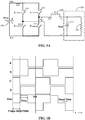
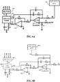
- FIG. 1A illustrates a basic diagram of a power stage for a dielectric barrier discharger in accordance with an embodiment of the invention.
- the four switches 121, 122, 123, and 124 are arranged as a full bridge to convert an incoming DC bus voltage input (Vbus) into a sinusoidal waveform through a parallel resonant tank network represented by resonant inductor Lr 105 and the ozone cell stack 110.
- Vbus DC bus voltage input
- the switches ( 121, 122, 123, and 124 ) can be any suitable switch, including, but not limited to, bipolar junction transistors (BJTs); insulated gate bipolar transistors (IGBTs); and field effect transistors (FETs), including MOSFETs (metal oxide semiconductor field effect transistors) and high electron mobility transistors (HEMTs).
- BJTs bipolar junction transistors
- IGBTs insulated gate bipolar transistors
- FETs field effect transistors
- MOSFETs metal oxide semiconductor field effect transistors
- HEMTs high electron mobility transistors
- a resonant tank (provided by the inductor 105 alone or in combination with the capacitor 111 of the load 110 ) receives the AC voltage from the full-bridge power source and provides a resonant (or substantially resonant) AC voltage in the form of a high voltage sine wave of controlled amplitude to the dielectric barrier discharge cell 110.
- a transformer (not shown in the diagram) can be included to step up the signal to the desired level. The effects of the transformer can be included in the simplified model by representing Vout as Vout/N, where N is the transformer turn ration.
- the cell(s) (or load) 110, of the dielectric barrier discharger can be modeled by the parallel capacitor 111 and resistor 112. Although the capacitor 111 is shown as part of the cell 110, the capacitance of this modeled capacitor may include a separate individual capacitor in addition to the natural capacitance of the cell.
- Figure 2A shows an electrical circuit model of an ozone cell stack that accounts for the voltage required at the output before ozone can be generated.
- a voltage clamp Do 213 (not shown in the basic diagram of Figure 1A ) can be included in series with the resistor 212 (modeled as resistor 112 of Figure 1A ) when modeling a dielectric barrier discharger cell that generates ozone. Because ozone concentration is proportional to the output power, an ozone cell can be modeled by the resistor 212 in series with the voltage clamp 213 (see also, for example, the resistor 312 and voltage clamp 313 shown in Figure 3 ).
- ozone can be generated after the output voltage reaches a certain voltage greater than the clamp's voltage, modeled as dissipation of power at resistor Ro 212. If the output voltage is less than the clamp's voltage (Do), then Ro 212 cannot conduct current to allow power dissipation and no ozone concentration is produced.
- Do clamp's voltage
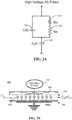
- Figure 2B provides a representation of one type of dielectric barrier discharger cell that may use the power stage configuration described herein to provide its high voltage AC power.
- the cell 200 can include a first electrode (not shown) that, upon application of AC power 201, generates an electrical discharge 202 from a first dielectric barrier film 203 across a gap 204 to a second electrode 205.
- An optional second dielectric barrier film (not shown) can be disposed on the second electrode 205. Water can be used to carry charge from the second electrode 205 to a ground.
- the first dielectric barrier film 203 is formed of alumina oxide (Al 2 O 3 ) and the second electrode 205 is formed of tungsten.
- oxygen (O 2 ) passing through the gap is broken down into atomic oxygen by the electric discharge across the gap, enabling the atomic oxygen to recombine into a mixture of ozone (O 3 ) and oxygen (O 2 ).
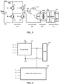
- FIG. 3 is a schematic diagram of a single power train with resonant inverter power stage according to an embodiment of the invention.
- the power train incorporates an electrical model of a dielectric barrier discharge cell that can be used to model an ozone generator in accordance with an embodiment of the invention.
- the switches of the power stage inverter 320 are implemented using IGBTs ( 321, 322, 323, and 324 ) arranged in a full bridge and that convert an incoming DC bus voltage input (Vbus) into a sinusoidal waveform through a parallel resonant tank network (via resonant tank 330, transformer 340, and ozone cell stacks 310 ).
- IGBTs are illustrated and described with respect to the embodiment shown in Figure 3 , it should be understood that embodiments are not limited thereto and other suitable transistor types may be used.
- the resonant tank 330 can include a blocking capacitor Cb 331 for protecting the full bridge IGBT of the power stage 320 and the high voltage transformer 340 from failure due to asymmetry in the driver circuit; a resonant inductor Lr 325 (which can include transformer leakage inductance); a high voltage step up transformer Xfm 340 (with magnetized inductance Lm 341 ); and an ozone load cell stack 310 (having capacitance Co 311, impedance Ro 312, and clamp voltage Do 313 ).
- the transformer output voltage can step up to about 8 kV pk-pk at around 30 kHz of switching frequency ( f sw) at a full output load operation.
- Q is selected to be less than 3. It should be understood that the components of the model are idealized (for the first order) while neglecting the high order harmonic (for the fundamental harmonic) to simplify the analysis.
- additional circuits may be included in the dielectric barrier discharge power system for purposes including, but not limited to, optimizing or improving component performance.
- a tuning circuit can be included that operates by tracing along the inverter output resonant tank's curve starting from a slightly higher frequency ( ⁇ 40 kHz) than the resonant frequency f res. The tracing halts when the desired input power is reached. This type of circuit can be referred to as a peak power point search circuit.
- the circuit is used to make sure that an individual inverter of the power stage produces the maximum output power.
- An exemplary embodiment of such a circuit is described in U.S. Patent Application Publication No. 2007/0108040 .
- This auto self-tuning design offers several advantages in coping with the inverter power stage's component tolerance; switching frequency variation; temperature variations; and ozone cell stack aging.
- control signal A drives the first switch 121
- control signal B drives the second switch 122
- control signal C drives the third switch 123
- control signal D drives the fourth switch 124.
- control signals A and D are used to respectively turn ON the first switch 121 and the fourth switch 124 for the lower rail of the sinusoidal waveform
- control signals B and C are used to respectively turn ON the second switch 122 and the third switch 123 for the higher rail of the sinusoidal waveform.
- a simplified timing diagram is shown in Figure 1B , which illustrates a zero voltage switch (ZVS) switching scheme and the resulting output response, in accordance with an embodiment of the invention.
- ZVS switching scheme is a soft switching technique. Soft switching techniques use resonant techniques to switch ON at zero voltage and to switch OFF at zero current. Negligible switching losses may occur in the devices.
- phase shifting in the control signals it is possible to minimize ringing in the output voltage caused by all switches being OFF.
- the amount phase shift used for the A and D control signals and the B and C control signals is a function of the system and can be any suitable phase shift for inhibiting ringing in the particular system in which the subject power stage is used.
- the power stage control signals A, B, C, and D are generated for phase shift ZVS through a combined pulse width modulation (PWM) and frequency modulation (FM) control scheme.
- PWM pulse width modulation
- FM frequency modulation
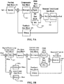
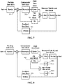
- FIG. 4 shows a block diagram of a dielectric barrier discharger system according to an embodiment of the invention.
- a power stage 410 converts a DC bus voltage V DC to an AC signal in order to supply a high voltage AC power to the load 420.
- the configuration of the power stage 410 and load 420 are arranged as shown in Figure 1A and/or Figure 3 .
- the power stage control signals A, B, C, and D are generated and controlled by the control circuit 430 that forms part of a feedback loop.
- the control circuit 430 can include a phase shift ZVS PWM combined with FM control.
- the signal generator for the power stage control signals is a phase-modulating and variable-frequency capable PWM chip.
- any circuit or chip that enables control of phase, duty cycle, and frequency may be used, where at least the duty cycle and frequency of the output signals can be adjusted by one or more inputs to the circuit or chip.
- the pulse width of the control signals A, B, C, and D is controlled by a PWM feedback control scheme of the control circuit 430 and the frequency of the control signals A, B, C, and D is controlled by a FM feedback control scheme of the control circuit 430.
- the PWM and FM feedback control scheme is implemented as a current loop control scheme, where an output current is sensed at an output of the power stage and used in controlling the pulse width and frequency of the signals provided back to the power stage.
- the integration of FM with the PWM control counteracts the light load hard switching of a solely PWM-based control scheme.
- Hard switching occurs because the inverter output voltage's pulse width greatly decreases at light loads. This then causes the resonant inductor's current to greatly decrease as well. Therefore, without sufficient stored energy in the resonant inductor, the semiconductor power devices can no longer sustain the soft switching.
- the combined PWM and FM control schemes along with the soft switching topology described herein reduces the need for additional cooling systems. For example, as mentioned above, when only PWM is used to control the switching signal, hard switching may occur at light loads. In contrast, the combined PWM and FM control scheme of embodiments of the invention enable soft switching through all loads (full and light).
- a "light load” condition depends on the particular system and is generally understood to be about 5% of full load. In practice, the particular percentage for light load is a percentage where ozone is still able to be generated. As illustrated by the examples in this disclosure, embodiments of the invention can operate at less than 5% of full load and function even when ozone is not being generated.
- the subject combined PWM and FM control scheme increases the frequency at light loads causing the previously decreasing pulse width to be negligible.
- the PWM and FM control scheme run in parallel, but the weight given to the PWM and the FM varies under changing load conditions. This results in an improved dynamic range performance. For example, at normal operation (including full load), the duty cycle is used to control the ozone output power; whereas for lighter loads, the power is further reduced by increasing the switching frequency.
- the power system power stage is configured, in certain embodiments, to soft-switch (e.g., by zero voltage switching) down to zero percent of maximum output power, reliability of the power system can be improved.
- Figure 5A shows a block diagram of a current loop control scheme according to one embodiment.
- the diagram provides transfer function blocks of each individual gain for the complete current loop control scheme.
- the function blocks include a Pre-Amp Gain Block 501, a current loop Compensation Gain Block 502, a PWM Gain Block 503, a FM Gain Block 504, a Resonant Tank & Load Gain Block 505, and a Feedback Gain Block 506.
- each individual gain block in the current loop can be expressed as follows:
- Kpwm ⁇ Kfm constant.
- a current set point is given a certain value. In certain embodiments, this can be accomplished using a processor (see description below with respect to Figure 5B ).
- the actual current (lout) output from the inverter power stage (see 410 of Figure 4 , and as shown in Figure 5A includes the Resonant Tank & Load Gain Block 505 ) can be measured by a current sensor and input to the feedback loop through Feedback Gain Block 506.
- the Iset that may be amplified via a pre-amp stage with corresponding Pre-Amp Gain Block 501
- the current (Ifbk) output from the Feedback Gain Block 506 are added at a current loop compensator with representative Gain Block 502.
- the output of this gain stage is then used by a phase shift PWM and FM Controller circuit or chip (having corresponding PWM Gain Block 503 and FM Gain Block 504 ) to produce a switching frequency (Fsw) for gate drivers (see Figures 6A and 6B ) of the power stage.
- the feedback loop performs in a manner to maintain the output current at a level equal to the Iset value.
- the output from the current loop Compensator Gain Block 503 is used to change the frequency time constant of the clock of the PWM chip, which allows frequency modulation to occur because the Fsw is inversely proportional to the time constant. Therefore, as the power on the line drops, the frequency modulation control lowers the frequency, enabling the power to be maintained at the appropriate levels.
- the current loop diagram shown in Figure 5A illustrates an analog control scheme.
- a digital control scheme can be utilized in place of or in addition to the analog control scheme shown in Figure 5A.
- Figure 5B provides a system level diagram with power loop and inner current loop of a control scheme for a ZVS resonant inverter.
- the current loop portion functions similarly to that described with respect to Figure 5A .
- the power loop uses a digital control scheme; and the power loop is implemented using a processor.
- the processor can be, but is not limited to, a low cost microprocessor ( ⁇ P) or a Digital Signal Processor (DSP). Memory can be included as part of the processor or as a separate component.
- ⁇ P low cost microprocessor
- DSP Digital Signal Processor
- the processor issues a power set point (Pset).
- Pset the actual input power is measured using the DC bus voltage (V DC of Figure 4 or Vbus shown in Figures 1 and 3 ) and the DC bus current (see Ibus in Figures 1 and 3 ), scaled with the gain from the two DC input sources (as Kvb(s) 508a and Kib(s) 508b ) and multiplied together for the input Power Gain Block.
- the product of the scaled and multiplied DC input sources results in the power feedback signal (Pfbk).
- the power set point Pset and the power feedback Pfbk are added together to feed a digital power loop compensator (PID).
- PID digital power loop compensator
- the output of the PID is the current set point Iset as described with respect to Figure 5A .
- the diagram shown in Figure 5B provides transfer function blocks of each individual gain for the complete power loop (with inner current loop) control scheme.
- the equation of each individual gain block in the current loop can be expressed as provided with respect to Figure 5A and the equation of each individual gain block for the power loop can be expressed as follows:
- output load power control may be used instead of controlling input power (and using the power loop illustrated in Figure 5B .
- the output ozone voltage and the inverter current sensed at the output of the inverter stage can be used as part of the control loop. Because the ozone cell behaves as a complex impedance and both the current and voltage are moderately high frequency, bandwidth, slew rate, sampling time, and other factors are needed in order to find the product of the current and the voltage in real time.
- the power loop shown in Figure 5B can be closed based on the ozone concentration.
- the ozone concentration from the ozone cells can be measured with a concentration transducer, the output of which can be used to close the power loop.
- Figures 6A and 6B illustrate two example current loop circuit implementations following the control scheme described with respect to Figure 5A .
- the current at the output of the inverter stage is measured by a current sensor 601 and fed (as Ifbk) to a current loop error amp compensator 602 along with Iset.
- Iset is provided as an input to a positive input terminal of the current loop error amp compensator 602 and Ifbk is provided as an input to a negative input terminal of the current loop error amp compensator 602.
- Iset and Ifbk are summed such that both are provided to the negative input terminal of the current loop error amp compensator 602.
- the output of the error amp compensator 602 provides the duty cycle command for the phase shift PWM controller 603 and also enables the PWM controller 603 to produce a switching frequency Fsw for the Gate Drivers 604.
- the switching frequency can be frequency modulated via an inverting amplifier 605 that receives the output of the error amp compensator 602 and outputs a signal to the PWM controller 603.
- the output of the inverting amplifier 605 changes the PWM clock's frequency time constant, allowing frequency modulation to occur.
- the Gate Drivers 604 produce the control signals A, B, C, and D for the full bridge inverter stage such as described with respect to Figures 1A-1B (switches 121, 122, 123, 124 ) and Figure 3 (switches 321, 322, 323, 324 of power stage 320 ).
- the capacitor Ct and the resistor Rt connected to the PWM controller 603 provide the initial fixed frequency that is adjusted by the current compensation signal from the inverting amplifier 605.
- the op-amp in the inverting amplifier configuration as shown in Figures 6A and 6B , can be used to adjust the signal used to control the frequency modulation with a multiple (or fraction) of the signal used to control the duty cycle (pulse width).
- the gain of the amplifier for the FM control can be varied by using a variable gain amplifier. The gain may be controlled using a gain control signal sent by the processor.
- preset modifications stored in a memory associated with the processor may be used when certain conditions in the system are met.
- a user interface may be included to enable user control of the gain adjustment. The user interface may be connected to and communicate with the processor. Alternatively, or in addition, the user interface may include a manual adjustment of resistance via a potentiometer (that may adjust, for example, R4 of Figure 6A or R4 of Figure 6B ).
- FIGs 7-9 illustrate current loop configurations in accordance with some embodiments of the invention.
- a current loop control scheme according to a second embodiment is similar to the scheme shown in Figure 5A .
- the FM Gain Block 704 stage accepts the Iset (that may be amplified via a pre-amp stage with corresponding Pre-Amp Gain Block 701 ) and the current (Ifbk) output from the Feedback Gain Block 706 in parallel with the current loop compensator.
- the FM Gain Block 804 stage uses the input power for controlling the frequency instead of the Iset current and the feedback current from the Feedback Gain Block 806 as described with respect to Figure 5A or Figure 7 .
- the DC bus voltage (V DC of Figure 4 or Vbus shown in Figures 1 and 3 ) and the DC bus current (see Ibus in Figures 1 and 3 ) are scaled with the gain from the two DC input sources (as Kvb(s) 808a and Kib(s) 808b ) and multiplied together before inputted through the FM Gain Block 804.
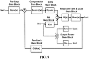
- the FM Gain Block 904 stage uses the output power for controlling the frequency instead of the input power as described with respect to Figure 8 .
- the power loop portion described with respect to Figure 5B can be configured with one of the current loops shown in Figures 7-9 .
- standards for accommodating power line variation while still maintaining power can be met without requiring extra circuitry or protective capacitors, which take up space and may require additional cooling techniques.
- frequency modulation control variation due to loads on the power line results in variation of the frequency driving the switches and the ability to maintain power on the line.
- SEMI F47 standard Standard "Specification for Semiconductor Processing Equipment Voltage Sag Immunity," which defines the voltage sag ride-through capability (or threshold) that a tool used in semiconductor processing, metrology, and automated test equipment must operate through without interruption.
- Embodiments of the subject power system and power control technique can be implemented without increasing the size of previous systems.
- the power system can fit into tighter spaces than traditional non-resident power converters while providing equal to or greater output power and control.
- the PSpice® circuit simulator tool a registered trademark of Cadence Design Systems, Inc., was used to simulate a dielectric barrier discharger designed in accordance with an embodiment of the invention.
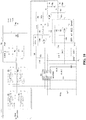
- FIG. 10 shows the PSpice® schematic used for the PSpice® simulations of a versatile ZVS Resonant Inverter current loop design in accordance with one embodiment of the invention.
- the schematic follows a similar implementation as that shown in Figure 6B where the feedback current and the current set point Iset are summed before being input to the compensator.
- the current is measured using differential amplifiers to avoid common mode noise.
- the resonant tank and ozone cell(s) are simulated using the inductor ( 105 ), capacitor ( 111 ), and resistor ( 112 ) configuration described with respect to Figure 1A .
- the input Vbus voltage was varied from low line to high line (200-350 VDC), and the Iset was varied by using a voltage source at 0.5-3.0 VDC (0.5% to 110% load). These two conditions cover the expected operating ranges.
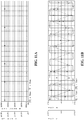
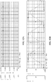
- Figure 11A-11C The simulation results for the current loop at light load are shown in Figures 11A-11C and the experimental results for the current loop at light load is shown in Figure 11D .
- Figure 11A shows that Vbus was set at 350 V, and the light load conditions show output load power being less than 25 W (compare to -250 W output power light load condition of 5% ozone concentration of a 5 kW system's maximum output).
- Figure 11B shows a plot of the inverter stage output voltage (Vinv) and current (Iinv).
- Figure 11C shows a plot of the power stage output voltage (Vout) and current (lout) (i.e., the voltage and current being supplied to the ozone cell(s)).
- Vbus 300 V
- Ibus 0.8 A
- Pin 240 W.
- the combination of PWM and FM control enable soft switching even at light loads. It should be noted that the scale for the plots for the simulation and the measurement result waveforms is not uniform because the simulation waveform was at 0.5% Iset while the experimental was at ⁇ 5% of Iset due to the process limitations for producing ozone.
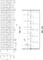
- Figure 12A shows that Vbus was set at 350 V, and the full load conditions show output load power being at about 5.5 kW (single stage).
- Figure 12B shows a plot of the inverter stage output voltage (Vinv) and current (Iinv).
- Figure 12C shows a plot of the power stage output voltage (Vout) and current (lout) (i.e., the voltage and current being supplied to the ozone cell(s)).
- Vbus 300 V
- Ibus 18.3 A
- Pin ⁇ 5.5 kW.
- the combination of PWM and FM control enable soft switching and increased output power.
Description
- Ozone is used for many industrial and semiconductor processing applications including, for example, cleaning semiconductor wafers and the process chambers of semiconductor processing equipment; producing insulating films on semiconductor wafers; and disinfecting water, food, and other consumable or industrial products.
- One technique for ozone generation involves a dielectric barrier discharge, where high purity oxygen is exposed to an electrical discharge created by the application of high voltage AC power. The electrical discharge breaks down the oxygen molecules into their atomic state, allowing the oxygen to recombine into a mixture of ozone (O3) and oxygen (O2). For this technique, ozone concentration is proportional to the output power of the ozone generating system. Although increasing output power increases ozone concentration, expectations of performance and reliability and limitations on space provide constraints that are often in opposition.
-
KR 100806624 B1 - A power system and power control technique for ozone generators and other dielectric barrier discharge systems are described herein. Various aspects of a dielectric barrier discharge power system and a method of generating dielectric barrier discharge are set out in the appended claims.
- According to certain embodiments, a power system is provided having a dual resonant inverter power stage using a parallel resonant topology instead of the traditional hard switching topology; and a combined pulse width modulation (PWM) and frequency modulation (FM) control scheme to achieve superior dynamic range and stability under any operations even at light load.
- A power system, according to one embodiment, includes an inverter stage providing a signal to a resonant tank and transformer that ultimately supplies a high voltage AC signal to one or more dielectric barrier discharge cells; and a feedback control circuit that provides the switching signals to the inverter stage. The inverter stage can be a full bridge operated with a phase shift Zero Voltage Switch (ZVS) and PWM combined with FM control via the feedback control circuit.
- According to one aspect of the invention, the power system and power control technique enable increased output power while providing the ability to operate from below the output power required for generating ozone through full power. In one embodiment, output power of a system operating in a range of 20 kHz to 40 kHz is increased from 5 kW to 10 kW, while providing the capability to operate at about 1% of the power system's maximum output up to full power (note: 5% ozone concentration of a 5 kW system's maximum output is ~ 250 W output power). In a specific embodiment, two power trains, each capable of 5 kW output power, are used to achieve the 10 kW output power.
- In a further aspect of the invention, the power system and power control technique are accomplished without increasing the size of previous systems. In one embodiment, the power system fits into a smaller space as compared to traditional non-resonant power converters.
- This Summary is provided to introduce a selection of concepts in a simplified form that are further described below in the Detailed Description. This Summary is not intended to identify key features or essential features of the claimed subject matter, nor is it intended to be used to limit the scope of the claimed subject matter.
-
-
FIG. 1A is a basic diagram of a power stage for a dielectric barrier discharger in accordance with an embodiment of the invention. -
FIG. 1B shows a set of plots of a soft switching scheme and resulting output of a power stage in accordance with an embodiment of the invention. -
FIG. 2A is an equivalent electrical model of an ozone cell stack. -
FIG. 2B is a representation of a dielectric barrier discharge cell for generating ozone for which a high voltage AC power signal can be supplied by a power system of an embodiment of the invention. -
FIG. 3 is a schematic diagram of a single power train with resonant inverter power stage according to an embodiment of the invention. -
FIG. 4 is a block diagram of a dielectric barrier discharger power system according to an embodiment of the invention. -
FIGS. 5A and 5B show basic block diagrams of a PWM and FM current loop control scheme (FIG. 5A ) and system level control scheme with power loop (FIG. 5B ) according to a first embodiment of the invention. -
FIG. 6A and 6B show schematic diagrams of the PWM and FM current loop control scheme shown inFIG. 5A according to certain embodiments of the invention. -
FIG. 7 shows a basic block diagram of a PWM and FM current loop control scheme according to a second embodiment of the invention. -
FIG. 8 shows a basic block diagram of a PWM and FM current loop control scheme according to a third embodiment of the invention. -
FIG. 9 shows a basic block diagram of a PWM and FM current loop control scheme according to a fourth embodiment of the invention. -
FIG. 10 is a simulation schematic of a ZVS resonant inverter current loop with PWM and FM control according to an embodiment of the invention. -
FIGS. 11A-11D show simulation plots and a scope waveform of an embodiment of the subject ZVS resonant inverter at light load conditions. -
FIGS. 12A-12D show simulation plots and a scope waveform of an embodiment of the subject ZVS resonant inverter at full load conditions. - Techniques and circuits are disclosed herein that enable improved control and power output for dielectric barrier dischargers, including ozone generators.
- According to an embodiment of the invention, a power system and power control technique is provided that enables increased output power while providing the ability to operate from below the output power required for generating ozone through full power. In accordance with a specific implementation of the subject invention, a power system frequency range of 20-40 kHz and output power of 10 kW with control to as low as ~1% of 10 kW is provided. In a specific embodiment, two power trains, each capable of 5 kW output power, are used to achieve the 10 kW output power.
-
Figure 1A illustrates a basic diagram of a power stage for a dielectric barrier discharger in accordance with an embodiment of the invention. In the power stage shown inFigure 1A , the fourswitches resonant inductor Lr 105 and theozone cell stack 110. The switches (121, 122, 123, and 124) can be any suitable switch, including, but not limited to, bipolar junction transistors (BJTs); insulated gate bipolar transistors (IGBTs); and field effect transistors (FETs), including MOSFETs (metal oxide semiconductor field effect transistors) and high electron mobility transistors (HEMTs). - A resonant tank (provided by the
inductor 105 alone or in combination with thecapacitor 111 of the load 110) receives the AC voltage from the full-bridge power source and provides a resonant (or substantially resonant) AC voltage in the form of a high voltage sine wave of controlled amplitude to the dielectricbarrier discharge cell 110. A transformer (not shown in the diagram) can be included to step up the signal to the desired level. The effects of the transformer can be included in the simplified model by representing Vout as Vout/N, where N is the transformer turn ration. - The cell(s) (or load) 110, of the dielectric barrier discharger can be modeled by the
parallel capacitor 111 andresistor 112. Although thecapacitor 111 is shown as part of thecell 110, the capacitance of this modeled capacitor may include a separate individual capacitor in addition to the natural capacitance of the cell. -
Figure 2A shows an electrical circuit model of an ozone cell stack that accounts for the voltage required at the output before ozone can be generated. In particular, a voltage clamp Do 213 (not shown in the basic diagram ofFigure 1A ) can be included in series with the resistor 212 (modeled asresistor 112 ofFigure 1A ) when modeling a dielectric barrier discharger cell that generates ozone. Because ozone concentration is proportional to the output power, an ozone cell can be modeled by theresistor 212 in series with the voltage clamp 213 (see also, for example, theresistor 312 andvoltage clamp 313 shown inFigure 3 ). In operation, ozone can be generated after the output voltage reaches a certain voltage greater than the clamp's voltage, modeled as dissipation of power atresistor Ro 212. If the output voltage is less than the clamp's voltage (Do), thenRo 212 cannot conduct current to allow power dissipation and no ozone concentration is produced. - The output capacitance Co (modeled as
capacitor 111 ofFigure 1A ) can be given as Co = Cd0*Cd1/(Cd0+Cd1), where Cd0 iscapacitor 211 in parallel with theseries voltage clamp 213 andresistor 212, and Cd1 iscapacitor 214 to ground. -
Figure 2B provides a representation of one type of dielectric barrier discharger cell that may use the power stage configuration described herein to provide its high voltage AC power. As shown inFigure 2B , thecell 200 can include a first electrode (not shown) that, upon application ofAC power 201, generates anelectrical discharge 202 from a firstdielectric barrier film 203 across agap 204 to asecond electrode 205. An optional second dielectric barrier film (not shown) can be disposed on thesecond electrode 205. Water can be used to carry charge from thesecond electrode 205 to a ground. In a specific embodiment, the firstdielectric barrier film 203 is formed of alumina oxide (Al2O3) and thesecond electrode 205 is formed of tungsten. - For ozone generation applications, oxygen (O2) passing through the gap is broken down into atomic oxygen by the electric discharge across the gap, enabling the atomic oxygen to recombine into a mixture of ozone (O3) and oxygen (O2).
-
Figure 3 is a schematic diagram of a single power train with resonant inverter power stage according to an embodiment of the invention. The power train incorporates an electrical model of a dielectric barrier discharge cell that can be used to model an ozone generator in accordance with an embodiment of the invention. As shown inFigure 3 , the switches of thepower stage inverter 320 are implemented using IGBTs (321, 322, 323, and 324) arranged in a full bridge and that convert an incoming DC bus voltage input (Vbus) into a sinusoidal waveform through a parallel resonant tank network (viaresonant tank 330,transformer 340, and ozone cell stacks 310). Although IGBTs are illustrated and described with respect to the embodiment shown inFigure 3 , it should be understood that embodiments are not limited thereto and other suitable transistor types may be used. - The
resonant tank 330 can include a blockingcapacitor Cb 331 for protecting the full bridge IGBT of thepower stage 320 and thehigh voltage transformer 340 from failure due to asymmetry in the driver circuit; a resonant inductor Lr 325 (which can include transformer leakage inductance); a high voltage step up transformer Xfm 340 (with magnetized inductance Lm 341); and an ozone load cell stack 310 (having capacitance Co 311,impedance Ro 312, and clamp voltage Do 313). With a 5kW single power train, the transformer output voltage can step up to about 8 kV pk-pk at around 30 kHz of switching frequency (fsw) at a full output load operation. The resonant tank's frequency fres can be given by

Figure 1A is valid. In certain embodiments, to inhibit recirculation of the resonant tank's current (energy loss), Q is selected to be less than 3. It should be understood that the components of the model are idealized (for the first order) while neglecting the high order harmonic (for the fundamental harmonic) to simplify the analysis. - Although not shown in the figures, additional circuits may be included in the dielectric barrier discharge power system for purposes including, but not limited to, optimizing or improving component performance. For example, within the power stage resonant tank's circuits, there may be variations in the components' tolerances, which can affect the fres in a manner degrading the performance of the power stage. Accordingly, in some embodiments, a tuning circuit can be included that operates by tracing along the inverter output resonant tank's curve starting from a slightly higher frequency (~40 kHz) than the resonant frequency fres. The tracing halts when the desired input power is reached. This type of circuit can be referred to as a peak power point search circuit. The circuit is used to make sure that an individual inverter of the power stage produces the maximum output power. An exemplary embodiment of such a circuit is described in
U.S. Patent Application Publication No. 2007/0108040 . This auto self-tuning design offers several advantages in coping with the inverter power stage's component tolerance; switching frequency variation; temperature variations; and ozone cell stack aging. - Referring again to
Figure 1A , control signal A drives thefirst switch 121, control signal B drives thesecond switch 122, control signal C drives thethird switch 123, and control signal D drives thefourth switch 124. In operation, control signals A and D are used to respectively turn ON thefirst switch 121 and thefourth switch 124 for the lower rail of the sinusoidal waveform and control signals B and C are used to respectively turn ON thesecond switch 122 and thethird switch 123 for the higher rail of the sinusoidal waveform. A simplified timing diagram is shown inFigure 1B , which illustrates a zero voltage switch (ZVS) switching scheme and the resulting output response, in accordance with an embodiment of the invention. A ZVS switching scheme is a soft switching technique. Soft switching techniques use resonant techniques to switch ON at zero voltage and to switch OFF at zero current. Negligible switching losses may occur in the devices. - As shown in
Figure 1B , by incorporating phase shifting in the control signals, it is possible to minimize ringing in the output voltage caused by all switches being OFF. The amount phase shift used for the A and D control signals and the B and C control signals is a function of the system and can be any suitable phase shift for inhibiting ringing in the particular system in which the subject power stage is used. - In accordance with various embodiments of the invention, the power stage control signals A, B, C, and D are generated for phase shift ZVS through a combined pulse width modulation (PWM) and frequency modulation (FM) control scheme.
-
Figure 4 shows a block diagram of a dielectric barrier discharger system according to an embodiment of the invention. Referring toFigure 4 , apower stage 410 converts a DC bus voltage VDC to an AC signal in order to supply a high voltage AC power to theload 420. In certain embodiments, the configuration of thepower stage 410 and load 420 are arranged as shown inFigure 1A and/orFigure 3 . The power stage control signals A, B, C, and D are generated and controlled by thecontrol circuit 430 that forms part of a feedback loop. Thecontrol circuit 430 can include a phase shift ZVS PWM combined with FM control. In certain embodiments, the signal generator for the power stage control signals is a phase-modulating and variable-frequency capable PWM chip. Of course, in some embodiments, any circuit or chip that enables control of phase, duty cycle, and frequency may be used, where at least the duty cycle and frequency of the output signals can be adjusted by one or more inputs to the circuit or chip. The pulse width of the control signals A, B, C, and D is controlled by a PWM feedback control scheme of thecontrol circuit 430 and the frequency of the control signals A, B, C, and D is controlled by a FM feedback control scheme of thecontrol circuit 430. In accordance with certain embodiments of the invention, the PWM and FM feedback control scheme is implemented as a current loop control scheme, where an output current is sensed at an output of the power stage and used in controlling the pulse width and frequency of the signals provided back to the power stage. - According to one embodiment, the integration of FM with the PWM control counteracts the light load hard switching of a solely PWM-based control scheme. Hard switching occurs because the inverter output voltage's pulse width greatly decreases at light loads. This then causes the resonant inductor's current to greatly decrease as well. Therefore, without sufficient stored energy in the resonant inductor, the semiconductor power devices can no longer sustain the soft switching.
- In hard switching, energy stored in the junction capacitance discharges into the transistor at each turn-on. Therefore, hard switching can cause power loss, voltage/current spikes, and electromagnetic interference (EMI) problems. The combined PWM and FM control schemes along with the soft switching topology described herein reduces the need for additional cooling systems. For example, as mentioned above, when only PWM is used to control the switching signal, hard switching may occur at light loads. In contrast, the combined PWM and FM control scheme of embodiments of the invention enable soft switching through all loads (full and light).
- A "light load" condition depends on the particular system and is generally understood to be about 5% of full load. In practice, the particular percentage for light load is a percentage where ozone is still able to be generated. As illustrated by the examples in this disclosure, embodiments of the invention can operate at less than 5% of full load and function even when ozone is not being generated.
- In operation, the subject combined PWM and FM control scheme increases the frequency at light loads causing the previously decreasing pulse width to be negligible. During operation, the PWM and FM control scheme run in parallel, but the weight given to the PWM and the FM varies under changing load conditions. This results in an improved dynamic range performance. For example, at normal operation (including full load), the duty cycle is used to control the ozone output power; whereas for lighter loads, the power is further reduced by increasing the switching frequency. In addition, because the power system power stage is configured, in certain embodiments, to soft-switch (e.g., by zero voltage switching) down to zero percent of maximum output power, reliability of the power system can be improved.
-
Figure 5A shows a block diagram of a current loop control scheme according to one embodiment. The diagram provides transfer function blocks of each individual gain for the complete current loop control scheme. The function blocks include aPre-Amp Gain Block 501, a current loopCompensation Gain Block 502, aPWM Gain Block 503, aFM Gain Block 504, a Resonant Tank &Load Gain Block 505, and aFeedback Gain Block 506. - According to one embodiment, the equation of each individual gain block in the current loop can be expressed as follows:
- "Pre-Amp gain Block:"

- Current Loop "Compensator Gain Block:"

- "Resonant Tank and Load Gain Block:"

- For example, Gpwr(s) = ωo 2/[s 2 + (1/Q)*ωo *s + ωo 2],
where
- Current "Feedback Gain Block:"

- For the PWM Gain Block and FM Gain Block, Kpwm ≠ Kfm = constant.
- Referring to
Figure 5A , a current set point (Iset) is given a certain value. In certain embodiments, this can be accomplished using a processor (see description below with respect toFigure 5B ). In addition, the actual current (lout) output from the inverter power stage (see 410 ofFigure 4 , and as shown inFigure 5A includes the Resonant Tank & Load Gain Block 505) can be measured by a current sensor and input to the feedback loop throughFeedback Gain Block 506. The Iset (that may be amplified via a pre-amp stage with corresponding Pre-Amp Gain Block 501) and the current (Ifbk) output from theFeedback Gain Block 506 are added at a current loop compensator withrepresentative Gain Block 502. The output of this gain stage is then used by a phase shift PWM and FM Controller circuit or chip (having correspondingPWM Gain Block 503 and FM Gain Block 504) to produce a switching frequency (Fsw) for gate drivers (seeFigures 6A and 6B ) of the power stage. The feedback loop performs in a manner to maintain the output current at a level equal to the Iset value. - In the case of light loads, the output from the current loop
Compensator Gain Block 503 is used to change the frequency time constant of the clock of the PWM chip, which allows frequency modulation to occur because the Fsw is inversely proportional to the time constant. Therefore, as the power on the line drops, the frequency modulation control lowers the frequency, enabling the power to be maintained at the appropriate levels. - The current loop diagram shown in
Figure 5A illustrates an analog control scheme. In another embodiment, such as shown inFigure 5B , a digital control scheme can be utilized in place of or in addition to the analog control scheme shown inFigure 5A. Figure 5B provides a system level diagram with power loop and inner current loop of a control scheme for a ZVS resonant inverter. The current loop portion functions similarly to that described with respect toFigure 5A . According to one embodiment, the power loop uses a digital control scheme; and the power loop is implemented using a processor. The processor can be, but is not limited to, a low cost microprocessor (µP) or a Digital Signal Processor (DSP). Memory can be included as part of the processor or as a separate component. In operation, the processor issues a power set point (Pset). In addition, the actual input power is measured using the DC bus voltage (VDC ofFigure 4 or Vbus shown inFigures 1 and3 ) and the DC bus current (see Ibus inFigures 1 and3 ), scaled with the gain from the two DC input sources (as Kvb(s) 508a and Kib(s) 508b) and multiplied together for the input Power Gain Block. The product of the scaled and multiplied DC input sources results in the power feedback signal (Pfbk). The power set point Pset and the power feedback Pfbk are added together to feed a digital power loop compensator (PID). The output of the PID is the current set point Iset as described with respect toFigure 5A . - As with
Figure 5A , the diagram shown inFigure 5B provides transfer function blocks of each individual gain for the complete power loop (with inner current loop) control scheme. According to one embodiment, the equation of each individual gain block in the current loop can be expressed as provided with respect toFigure 5A and the equation of each individual gain block for the power loop can be expressed as follows: - "Digital Power Loop Compensator Gain Block:"

- Where z = e s/Fclk ; Fclk = µP_Clock (frequency of the clock from the processor).
- It should be understood that the components of the models are idealized (for the first order) while neglecting the high order harmonic (for the fundamental harmonic) to simplify the analysis.
- In another embodiment, instead of controlling input power (and using the power loop illustrated in
Figure 5B , output load power control may be used. For example, the output ozone voltage and the inverter current sensed at the output of the inverter stage can be used as part of the control loop. Because the ozone cell behaves as a complex impedance and both the current and voltage are moderately high frequency, bandwidth, slew rate, sampling time, and other factors are needed in order to find the product of the current and the voltage in real time. - In yet another embodiment, the power loop shown in
Figure 5B can be closed based on the ozone concentration. For example, the ozone concentration from the ozone cells can be measured with a concentration transducer, the output of which can be used to close the power loop. -
Figures 6A and 6B illustrate two example current loop circuit implementations following the control scheme described with respect toFigure 5A . As shown inFigures 6A and 6B , the current at the output of the inverter stage is measured by acurrent sensor 601 and fed (as Ifbk) to a current looperror amp compensator 602 along with Iset. In one embodiment, as shown inFigure 6A , Iset is provided as an input to a positive input terminal of the current looperror amp compensator 602 and Ifbk is provided as an input to a negative input terminal of the current looperror amp compensator 602. In another embodiment, as shown inFigure 6B , Iset and Ifbk are summed such that both are provided to the negative input terminal of the current looperror amp compensator 602. The output of theerror amp compensator 602 provides the duty cycle command for the phaseshift PWM controller 603 and also enables thePWM controller 603 to produce a switching frequency Fsw for theGate Drivers 604. The switching frequency can be frequency modulated via an invertingamplifier 605 that receives the output of theerror amp compensator 602 and outputs a signal to thePWM controller 603. The output of the invertingamplifier 605 changes the PWM clock's frequency time constant, allowing frequency modulation to occur. - The
Gate Drivers 604 produce the control signals A, B, C, and D for the full bridge inverter stage such as described with respect toFigures 1A-1B (switches 121, 122, 123, 124) andFigure 3 (switches - The capacitor Ct and the resistor Rt connected to the
PWM controller 603 provide the initial fixed frequency that is adjusted by the current compensation signal from the invertingamplifier 605. The op-amp, in the inverting amplifier configuration as shown inFigures 6A and 6B , can be used to adjust the signal used to control the frequency modulation with a multiple (or fraction) of the signal used to control the duty cycle (pulse width). In a further embodiment, the gain of the amplifier for the FM control can be varied by using a variable gain amplifier. The gain may be controlled using a gain control signal sent by the processor. In one embodiment, preset modifications stored in a memory associated with the processor may be used when certain conditions in the system are met. In another embodiment, a user interface may be included to enable user control of the gain adjustment. The user interface may be connected to and communicate with the processor. Alternatively, or in addition, the user interface may include a manual adjustment of resistance via a potentiometer (that may adjust, for example, R4 ofFigure 6A or R4 ofFigure 6B ). -
Figures 7-9 illustrate current loop configurations in accordance with some embodiments of the invention. For example, referring toFigure 7 , a current loop control scheme according to a second embodiment is similar to the scheme shown inFigure 5A . However, instead of the output of theCompensator Gain Block 702 stage being used by both the phase shift PWM and FM Controller to produce a switching frequency (Fsw) for the Gate Drivers (see 604 ofFigures 6A and 6B ) of the power stage, theFM Gain Block 704 stage accepts the Iset (that may be amplified via a pre-amp stage with corresponding Pre-Amp Gain Block 701) and the current (Ifbk) output from the Feedback Gain Block 706 in parallel with the current loop compensator. - For the embodiment shown in
Figure 8 , theFM Gain Block 804 stage uses the input power for controlling the frequency instead of the Iset current and the feedback current from theFeedback Gain Block 806 as described with respect toFigure 5A orFigure 7 . For example, the DC bus voltage (VDC ofFigure 4 or Vbus shown inFigures 1 and3 ) and the DC bus current (see Ibus inFigures 1 and3 ) are scaled with the gain from the two DC input sources (as Kvb(s) 808a and Kib(s) 808b) and multiplied together before inputted through theFM Gain Block 804. - For the embodiment shown in
Figure 9 , theFM Gain Block 904 stage uses the output power for controlling the frequency instead of the input power as described with respect toFigure 8 . - In certain embodiments, the power loop portion described with respect to
Figure 5B can be configured with one of the current loops shown inFigures 7-9 . - Advantageously, in certain embodiments, standards for accommodating power line variation while still maintaining power can be met without requiring extra circuitry or protective capacitors, which take up space and may require additional cooling techniques. In particular, by using frequency modulation control, variation due to loads on the power line results in variation of the frequency driving the switches and the ability to maintain power on the line. One example of a standard that can be met by the subject combined PWM and FM control scheme is the SEMI F47 standard "Specification for Semiconductor Processing Equipment Voltage Sag Immunity," which defines the voltage sag ride-through capability (or threshold) that a tool used in semiconductor processing, metrology, and automated test equipment must operate through without interruption.
- Embodiments of the subject power system and power control technique can be implemented without increasing the size of previous systems. In various embodiments, the power system can fit into tighter spaces than traditional non-resident power converters while providing equal to or greater output power and control.
- A greater understanding of the present invention and of its many advantages may be had from the following examples, given by way of illustration. The following examples are illustrative of some of the methods, applications, embodiments and variants of the present invention. They are, of course, not to be considered in any way limitative of the invention. Numerous changes and modifications can be made with respect to the invention.
- The PSpice® circuit simulator tool, a registered trademark of Cadence Design Systems, Inc., was used to simulate a dielectric barrier discharger designed in accordance with an embodiment of the invention.
- In the examples, the PSpice® simulations for a dual 10 kW ozone power train (5 kW per power train) are compared to experimental results to illustrate the functionality of the subject systems and methods.
Figure 10 shows the PSpice® schematic used for the PSpice® simulations of a versatile ZVS Resonant Inverter current loop design in accordance with one embodiment of the invention. The schematic follows a similar implementation as that shown inFigure 6B where the feedback current and the current set point Iset are summed before being input to the compensator. In addition, the current is measured using differential amplifiers to avoid common mode noise. The resonant tank and ozone cell(s) are simulated using the inductor (105), capacitor (111), and resistor (112) configuration described with respect toFigure 1A . - For the simulations, the input Vbus voltage was varied from low line to high line (200-350 VDC), and the Iset was varied by using a voltage source at 0.5-3.0 VDC (0.5% to 110% load). These two conditions cover the expected operating ranges.
- The simulation results for the current loop at light load are shown in
Figures 11A-11C and the experimental results for the current loop at light load is shown inFigure 11D .Figure 11A shows that Vbus was set at 350 V, and the light load conditions show output load power being less than 25 W (compare to -250 W output power light load condition of 5% ozone concentration of a 5 kW system's maximum output).Figure 11B shows a plot of the inverter stage output voltage (Vinv) and current (Iinv).Figure 11C shows a plot of the power stage output voltage (Vout) and current (lout) (i.e., the voltage and current being supplied to the ozone cell(s)).Figure 11D shows the scope waveforms of the inverter stage output voltage Vinv and current Iinv for the experimental system where Vbus = 300 V, Ibus = 0.8 A, Pin = 240 W. As illustrated byFigure 11C and confirmed by the waveforms shown inFigure 11D , the combination of PWM and FM control enable soft switching even at light loads. It should be noted that the scale for the plots for the simulation and the measurement result waveforms is not uniform because the simulation waveform was at 0.5% Iset while the experimental was at ∼5% of Iset due to the process limitations for producing ozone. - The simulation results for the current loop at full load are shown in
Figures 12A-12C and the experimental results for the current loop at 110% of full load is shown inFigure 12D .Figure 12A shows that Vbus was set at 350 V, and the full load conditions show output load power being at about 5.5 kW (single stage).Figure 12B shows a plot of the inverter stage output voltage (Vinv) and current (Iinv).Figure 12C shows a plot of the power stage output voltage (Vout) and current (lout) (i.e., the voltage and current being supplied to the ozone cell(s)).Figure 12D shows the scope waveforms of the inverter stage output voltage Vinv and current Iinv for the experimental system where Vbus = 300 V, Ibus = 18.3 A, Pin = ~5.5 kW. As illustrated byFigure 12C and confirmed by the waveforms shown inFigure 12D , the combination of PWM and FM control enable soft switching and increased output power.
Claims (15)
- A dielectric barrier discharge power system comprising:an inverter stage (320, 410);a resonant tank (330) receiving an output of the inverter stage and outputting a signal for powering at least one dielectric barrier discharge cell; anda control circuit (430) comprising:a gate driver (604) providing switching signals to the inverter stage, the switching signals including a phase shift for soft switching; anda pulse width modulation "PWM" controller (603) for generating a switching frequency for the gate driver, the PWM controller having a first input configured to receive a first signal for adjusting a duty cycle of the switching frequency to perform PWM and a second input configured to receive a second signal for adjusting a clock frequency time constant of the PWM controller to perform frequency modulation "FM";wherein the control circuit receives a feedback signal comprising an output current from the inverter stage (320, 410) and uses the feedback signal to generate the first signal and the second signal; characterised in that the control circuit is configured such that an amount of weight given to the PWM and the FM for controlling power changes as the dielectric barrier discharge power system operates from a full load condition to a light load condition.
- The dielectric barrier discharge power system according to claim 1, wherein the inverter stage (320) comprises four transistors (321, 322, 323, and 324) arranged as a full bridge, optionally wherein the four transistors are insulated gate bipolar transistors "IGBTs".
- The dielectric barrier discharge power system according to claim 1, further comprising a transformer (340) stepping up the signal from the resonant tank for powering the at least one dielectric barrier discharge cell.
- The dielectric barrier discharge power system according to claim 1, wherein the switching frequency is in a range of 20 kHz to 40 kHz or configured to be higher than a resonant frequency of the resonant tank (330).
- The dielectric barrier discharge power system according to claim 1, wherein the feedback signal comprises a measured current signal received from a current sensor at the output of the inverter stage (320).
- The dielectric barrier discharge power system according to claim 5, wherein
during all load conditions, the measured current signal is compared to a current set point value and an error value of the comparison causes the first signal to adjust the duty cycle of the switching frequency to perform the PWM until the measured current reaches the current set point value, the error value of the comparison further causing the second signal to adjust the clock frequency time constant to change to perform the FM. - The dielectric barrier discharge power system according to claim 5, wherein the control circuit (430) comprises a current control loop for generating the first signal and the second signal, the current control loop using the measured current signal sensed at the output of the inverter stage (320) and a current set point.
- The dielectric barrier discharge power system according to claim 7, wherein the current control loop comprises:an error amplifier compensator (602) receiving the measured current signal and the current set point and outputting the first signal; andone of an inverting amplifier (605) receiving the first signal and outputting the second signal or an inverting amplifier (605) receiving an added signal of the measured current signal and a current set point and outputting the second signal.
- The dielectric barrier discharge power system according to claim 7, wherein the feedback signal further comprises one of:an input power signal, the input power signal being a product of a measured DC bus voltage supplied to the inverter stage (320) and a measured DC bus current supplied to the inverter stage (320), oran output power signal, the output power signal being a product of a measured DC output voltage and the measured current; andwherein the current control loop comprises:an error amplifier compensator (602) receiving the measured current and the current set point and outputting the first signal; andan inverting amplifier (605) receiving the input power signal and outputting the second signal.
- The dielectric barrier discharge power system according to claim 7, further comprising a processor configured to:receive a measurement of a DC bus voltage and current supplied to the inverter stage (320), the measurement of the DC bus voltage and the current being scaled and multiplied together to provide a power feedback signal;add the power feedback signal to a power set point; andperform a digital error compensation using the power feedback signal and the power set point to output the current set point for the current control loop.
- A method of generating dielectric barrier discharge, the method comprising:providing an inverter stage (320) and resonant tank (330) for powering at least one dielectric barrier discharge cell (110); andgenerating switching signals for the inverter stage (320) using a control circuit (430), the switching signals including a phase shift for soft switching, wherein generating the switching signals comprises:performing pulse width modulation "PWM" of a switching frequency of the switching signals to maintain an output current of the inverter stage (320) at a current set point value; andperforming frequency modulation "FM" in parallel with performing the PWM by adjusting a clock frequency time constant of the PWM controller, and varying an amount of weight given to the PWM and the FM under changing load conditions.
- The method according to claim 11, wherein the switching signals have a frequency in a range of 20 kHz to 40 kHz.
- The method according to claim 11, wherein performing the PWM comprises:providing a PWM controller (603) for generating the switching frequency for a gate driver (604), the PWM controller having a first input configured to receive a first signal for adjusting a duty cycle of the switching frequency to perform PWM and a second input configured to receive a second signal for adjusting a clock frequency time constant of the PWM controller (603) to perform FM;sensing the output current of the inverter stage (320);comparing the output current to a current set point by performing error amplifier compensation; andusing the error amplifier compensation as the first signal.
- The method according to claim 13, wherein performing the FM comprises:inverting the error amplifier compensation using an inverting amplifier (605), the inverting amplifier outputting the second signal,optionally wherein performing the FM further comprises: adjusting a gain of the inverting amplifier (605).
- The method according to claim 13, further comprising:receiving a measurement of a DC bus voltage supplied to the inverter stage (320) and a measurement of a DC bus current supplied to the inverter stage (320), the measurements of the DC bus voltage and the DC bus current being scaled and multiplied together to provide a power feedback signal;adding the power feedback signal to a power set point; andperforming a digital error compensation using the power feedback signal and the power set point to output the current set point.
Applications Claiming Priority (2)
| Application Number | Priority Date | Filing Date | Title |
|---|---|---|---|
| US13/431,521 US8680777B2 (en) | 2012-03-27 | 2012-03-27 | Versatile zero-voltage switch resonant inverter for industrial dielectric barrier discharge generator applications |
| PCT/US2013/032772 WO2013148390A1 (en) | 2012-03-27 | 2013-03-18 | A versatile zero-voltage switch resonant inverter for industrial dielectric barrier discharge generator applications |
Publications (3)
| Publication Number | Publication Date |
|---|---|
| EP2834911A1 EP2834911A1 (en) | 2015-02-11 |
| EP2834911A4 EP2834911A4 (en) | 2016-03-30 |
| EP2834911B1 true EP2834911B1 (en) | 2019-01-09 |
Family
ID=49233996
Family Applications (1)
| Application Number | Title | Priority Date | Filing Date |
|---|---|---|---|
| EP13768401.5A Active EP2834911B1 (en) | 2012-03-27 | 2013-03-18 | A versatile zero-voltage switch resonant inverter for industrial dielectric barrier discharge generator applications |
Country Status (8)
| Country | Link |
|---|---|
| US (1) | US8680777B2 (en) |
| EP (1) | EP2834911B1 (en) |
| JP (1) | JP5923658B2 (en) |
| KR (1) | KR101665220B1 (en) |
| CN (1) | CN104205604B (en) |
| SG (1) | SG11201404303PA (en) |
| TW (1) | TWI551026B (en) |
| WO (1) | WO2013148390A1 (en) |
Families Citing this family (52)
| Publication number | Priority date | Publication date | Assignee | Title |
|---|---|---|---|---|
| US20140008211A1 (en) | 2012-07-06 | 2014-01-09 | Pacific Ozone Technology, Inc. | Ozone cell power supply apparatus and method |
| US9363862B1 (en) * | 2012-12-05 | 2016-06-07 | Universal Lighting Technologies | Automatic current and reference gain control for wide range current control |
| US9263960B2 (en) * | 2013-09-16 | 2016-02-16 | Delta Electronics, Inc. | Power converters for wide input or output voltage range and control methods thereof |
| US9844127B2 (en) | 2014-01-10 | 2017-12-12 | Reno Technologies, Inc. | High voltage switching circuit |
| US10431428B2 (en) | 2014-01-10 | 2019-10-01 | Reno Technologies, Inc. | System for providing variable capacitance |
| US10455729B2 (en) | 2014-01-10 | 2019-10-22 | Reno Technologies, Inc. | Enclosure cooling system |
| US9755641B1 (en) | 2014-01-10 | 2017-09-05 | Reno Technologies, Inc. | High speed high voltage switching circuit |
| US9196459B2 (en) | 2014-01-10 | 2015-11-24 | Reno Technologies, Inc. | RF impedance matching network |
| US9697991B2 (en) | 2014-01-10 | 2017-07-04 | Reno Technologies, Inc. | RF impedance matching network |
| US9865432B1 (en) | 2014-01-10 | 2018-01-09 | Reno Technologies, Inc. | RF impedance matching network |
| US9496122B1 (en) | 2014-01-10 | 2016-11-15 | Reno Technologies, Inc. | Electronically variable capacitor and RF matching network incorporating same |
| EP3204997A4 (en) * | 2014-10-08 | 2018-02-14 | PowerbyProxi Limited | Inverter for inductive power transmitter |
| US9525412B2 (en) | 2015-02-18 | 2016-12-20 | Reno Technologies, Inc. | Switching circuit |
| US9306533B1 (en) | 2015-02-20 | 2016-04-05 | Reno Technologies, Inc. | RF impedance matching network |
| US10340879B2 (en) | 2015-02-18 | 2019-07-02 | Reno Technologies, Inc. | Switching circuit |
| US9729122B2 (en) | 2015-02-18 | 2017-08-08 | Reno Technologies, Inc. | Switching circuit |
| US11017983B2 (en) | 2015-02-18 | 2021-05-25 | Reno Technologies, Inc. | RF power amplifier |
| US10692699B2 (en) | 2015-06-29 | 2020-06-23 | Reno Technologies, Inc. | Impedance matching with restricted capacitor switching |
| US11342161B2 (en) | 2015-06-29 | 2022-05-24 | Reno Technologies, Inc. | Switching circuit with voltage bias |
| US11342160B2 (en) | 2015-06-29 | 2022-05-24 | Reno Technologies, Inc. | Filter for impedance matching |
| US11081316B2 (en) | 2015-06-29 | 2021-08-03 | Reno Technologies, Inc. | Impedance matching network and method |
| US11335540B2 (en) | 2015-06-29 | 2022-05-17 | Reno Technologies, Inc. | Impedance matching network and method |
| US10984986B2 (en) | 2015-06-29 | 2021-04-20 | Reno Technologies, Inc. | Impedance matching network and method |
| US11150283B2 (en) | 2015-06-29 | 2021-10-19 | Reno Technologies, Inc. | Amplitude and phase detection circuit |
| US10680457B2 (en) * | 2015-07-27 | 2020-06-09 | Witricity Corporation | Systems, methods, and apparatus implementing hybrid symmetric and asymmetric control for soft switching in wireless power transfer applications |
| US9648716B2 (en) * | 2015-09-02 | 2017-05-09 | Mks Instruments, Inc. | Direct three phase parallel resonant inverter for reactive gas generator applications |
| TWI575855B (en) * | 2016-03-25 | 2017-03-21 | Resonance control device | |
| CN106301050B (en) * | 2016-08-30 | 2019-04-09 | 辽宁开普医疗系统有限公司 | Series parallel resonance inverter control circuit and its control method |
| JP6772922B2 (en) * | 2017-03-24 | 2020-10-21 | 株式会社デンソー | Resonant inverter |
| US11114280B2 (en) | 2017-07-10 | 2021-09-07 | Reno Technologies, Inc. | Impedance matching with multi-level power setpoint |
| US11315758B2 (en) | 2017-07-10 | 2022-04-26 | Reno Technologies, Inc. | Impedance matching using electronically variable capacitance and frequency considerations |
| US11393659B2 (en) | 2017-07-10 | 2022-07-19 | Reno Technologies, Inc. | Impedance matching network and method |
| US10727029B2 (en) | 2017-07-10 | 2020-07-28 | Reno Technologies, Inc | Impedance matching using independent capacitance and frequency control |
| US11476091B2 (en) | 2017-07-10 | 2022-10-18 | Reno Technologies, Inc. | Impedance matching network for diagnosing plasma chamber |
| US10483090B2 (en) | 2017-07-10 | 2019-11-19 | Reno Technologies, Inc. | Restricted capacitor switching |
| US11289307B2 (en) | 2017-07-10 | 2022-03-29 | Reno Technologies, Inc. | Impedance matching network and method |
| US10714314B1 (en) | 2017-07-10 | 2020-07-14 | Reno Technologies, Inc. | Impedance matching network and method |
| US11101110B2 (en) | 2017-07-10 | 2021-08-24 | Reno Technologies, Inc. | Impedance matching network and method |
| US11398370B2 (en) | 2017-07-10 | 2022-07-26 | Reno Technologies, Inc. | Semiconductor manufacturing using artificial intelligence |
| US11521833B2 (en) | 2017-07-10 | 2022-12-06 | Reno Technologies, Inc. | Combined RF generator and RF solid-state matching network |
| EP3518257A1 (en) * | 2018-01-26 | 2019-07-31 | FRIWO Gerätebau GmbH | Transformer unit for a resonant converter |
| CN108964438B (en) * | 2018-07-19 | 2020-11-06 | 中山大学 | Ozone generation power supply start control device and method and ozone generation device |
| TWI671984B (en) * | 2018-11-14 | 2019-09-11 | 群光電能科技股份有限公司 | Power supply device |
| CN109795347B (en) * | 2019-01-08 | 2022-06-21 | 狐灵灵智能科技有限公司 | Wireless intelligent charging method for electric bicycle |
| US11521831B2 (en) | 2019-05-21 | 2022-12-06 | Reno Technologies, Inc. | Impedance matching network and method with reduced memory requirements |
| CN110880857A (en) * | 2019-10-29 | 2020-03-13 | 南宁市跃龙科技有限公司 | High-power frequency conversion inversion system of medical X-ray high-voltage generator |
| GB202018200D0 (en) * | 2020-11-19 | 2021-01-06 | Daphne Tech Sa | Circuit |
| CN112410801A (en) * | 2021-01-22 | 2021-02-26 | 四川大学 | Water electrolysis hydrogen production system of current source type PWM rectifier and control method |
| CN113435041B (en) * | 2021-06-24 | 2023-09-22 | 平顶山学院 | Dielectric barrier discharge load electrical model parameter identification method, device and equipment |
| GB2605212A (en) * | 2021-07-16 | 2022-09-28 | Daphne Tech Sa | Apparatus and method for electron irradiation scrubbing |
| TWI783819B (en) * | 2021-12-13 | 2022-11-11 | 新唐科技股份有限公司 | Inductive current sensor, constant peak current circuit and dc-dc conversion apparatus |
| CN114337316A (en) * | 2022-01-14 | 2022-04-12 | 张全星 | Self-adaptive multi-phase output high-voltage power supply |
Family Cites Families (11)
| Publication number | Priority date | Publication date | Assignee | Title |
|---|---|---|---|---|
| JP3521731B2 (en) * | 1998-02-13 | 2004-04-19 | ウシオ電機株式会社 | Dielectric barrier discharge lamp light source device |
| JP2003230280A (en) * | 2002-01-30 | 2003-08-15 | Toshiba Corp | Power converter |
| JP2005123008A (en) * | 2003-10-16 | 2005-05-12 | Harison Toshiba Lighting Corp | Driving device for dielectric barrier type low-pressure discharge lamp |
| CN100589675C (en) * | 2004-03-29 | 2010-02-10 | 三菱电机株式会社 | Plasma generation power supply apparatus |
| JP2005333726A (en) | 2004-05-20 | 2005-12-02 | Toshiba Corp | Method of controlling frequency of dc-dc converter and switching power source |
| JP4667836B2 (en) * | 2004-11-26 | 2011-04-13 | 株式会社リコー | Switching regulator and switching regulator output voltage switching method |
| KR101323046B1 (en) * | 2005-08-16 | 2013-10-29 | 엠케이에스 인스트루먼츠, 인코포레이티드 | Load resonant type power supply for ozonizer |
| KR100806624B1 (en) * | 2007-02-21 | 2008-02-25 | (주) 이이시스 | Device for controlling high voltage having capacitive load property |
| JP5010455B2 (en) * | 2007-12-25 | 2012-08-29 | ハリソン東芝ライティング株式会社 | Dielectric barrier discharge lamp lighting device |
| JP5193086B2 (en) * | 2008-07-04 | 2013-05-08 | 株式会社荏原製作所 | Discharge cell discharge circuit and discharge cell discharge circuit control system |
| KR100891506B1 (en) * | 2009-01-30 | 2009-04-06 | (주)인텍에프에이 | Power converter for ozone generator and method for controlling the same |
-
2012
- 2012-03-27 US US13/431,521 patent/US8680777B2/en active Active
-
2013
- 2013-03-13 TW TW102108925A patent/TWI551026B/en active
- 2013-03-18 EP EP13768401.5A patent/EP2834911B1/en active Active
- 2013-03-18 CN CN201380014703.3A patent/CN104205604B/en active Active
- 2013-03-18 SG SG11201404303PA patent/SG11201404303PA/en unknown
- 2013-03-18 WO PCT/US2013/032772 patent/WO2013148390A1/en active Application Filing
- 2013-03-18 KR KR1020147029941A patent/KR101665220B1/en active IP Right Grant
- 2013-03-18 JP JP2015503359A patent/JP5923658B2/en active Active
Non-Patent Citations (1)
| Title |
|---|
| None * |
Also Published As
| Publication number | Publication date |
|---|---|
| US20130257311A1 (en) | 2013-10-03 |
| KR20140148443A (en) | 2014-12-31 |
| CN104205604A (en) | 2014-12-10 |
| TW201340578A (en) | 2013-10-01 |
| TWI551026B (en) | 2016-09-21 |
| JP5923658B2 (en) | 2016-05-24 |
| KR101665220B1 (en) | 2016-10-11 |
| EP2834911A4 (en) | 2016-03-30 |
| SG11201404303PA (en) | 2014-09-26 |
| CN104205604B (en) | 2017-11-14 |
| US8680777B2 (en) | 2014-03-25 |
| JP2015514385A (en) | 2015-05-18 |
| WO2013148390A1 (en) | 2013-10-03 |
| EP2834911A1 (en) | 2015-02-11 |
Similar Documents
| Publication | Publication Date | Title |
|---|---|---|
| EP2834911B1 (en) | A versatile zero-voltage switch resonant inverter for industrial dielectric barrier discharge generator applications | |
| Villar et al. | Optimal design and experimental validation of a Medium-Frequency 400kVA power transformer for railway traction applications | |
| Li et al. | Flying-capacitor-based hybrid LLC converters with input voltage autobalance ability for high voltage applications | |
| Segaran | Dynamic modelling and control of dual active bridge bi-directional dc-dc converters for smart grid applications | |
| JP2011528794A (en) | Circuit for simulating electrical loads | |
| Ibanez et al. | Novel technique for bidirectional series‐resonant DC/DC converter in discontinuous mode | |
| JP4735188B2 (en) | Power converter | |
| CN109478849B (en) | Resonant power conversion device | |
| Tang et al. | Comprehensive study of fast load modulation with volt‐second balance in a dual‐active‐bridge converter | |
| JP2009277577A (en) | Operation method of power supply device for induction heating | |
| Aalami et al. | High‐voltage gain magnetically coupled half‐bridge Z‐source inverter | |
| Samsudin et al. | Full-bridge LLC resonant high-voltage DC–DC converter with hybrid symmetrical voltage multiplier | |
| JP2014205190A (en) | Power source device and power source device for arc processing | |
| Moradi Ghahderijani et al. | Robust and Fast sliding‐mode control for a DC–DC current‐source parallel‐resonant converter | |
| Uddin et al. | Compact wireless IPT system using a modified voltage-fed multi-resonant class EF 2 inverter | |
| Jiang et al. | Novel modeling and design of a dual half bridge DC-DC converter applied in supercapacitor energy storage system | |
| Huisman et al. | Optimal trajectory control of a CLCC resonant power converter | |
| Yu et al. | Drain-source synchronous rectifier oscillation mitigation in light-load conditions | |
| Chae et al. | Pulse current generator with improved waveform fidelity for high-voltage capacitively coupled plasma systems | |
| JP2010081697A (en) | Resonance type power conversion device | |
| Shin et al. | Considerations on the DBD power supply for surface change of ozone reactor | |
| Kimpara et al. | Design of Auxiliary Power Supply for Medium Voltage Applications | |
| Nguyen-Duy et al. | Design of a 300-Watt isolated power supply with minimized circuit input-to-output parasitic capacitance | |
| Samal et al. | Non Isolated Multi Port Inverter with Reduced Common Mode Leakage Current and Minimum Phase Property | |
| Surkanti et al. | High-efficiency, high-dimming ratio LED driver |
Legal Events
| Date | Code | Title | Description |
|---|---|---|---|
| PUAI | Public reference made under article 153(3) epc to a published international application that has entered the european phase |
Free format text: ORIGINAL CODE: 0009012 |
|
| 17P | Request for examination filed |
Effective date: 20140923 |
|
| AK | Designated contracting states |
Kind code of ref document: A1 Designated state(s): AL AT BE BG CH CY CZ DE DK EE ES FI FR GB GR HR HU IE IS IT LI LT LU LV MC MK MT NL NO PL PT RO RS SE SI SK SM TR |
|
| AX | Request for extension of the european patent |
Extension state: BA ME |
|
| DAX | Request for extension of the european patent (deleted) | ||
| RA4 | Supplementary search report drawn up and despatched (corrected) |
Effective date: 20160226 |
|
| RIC1 | Information provided on ipc code assigned before grant |
Ipc: H02M 7/48 20070101AFI20160222BHEP |
|
| STAA | Information on the status of an ep patent application or granted ep patent |
Free format text: STATUS: EXAMINATION IS IN PROGRESS |
|
| 17Q | First examination report despatched |
Effective date: 20170518 |
|
| GRAP | Despatch of communication of intention to grant a patent |
Free format text: ORIGINAL CODE: EPIDOSNIGR1 |
|
| STAA | Information on the status of an ep patent application or granted ep patent |
Free format text: STATUS: GRANT OF PATENT IS INTENDED |
|
| INTG | Intention to grant announced |
Effective date: 20180808 |
|
| RIN1 | Information on inventor provided before grant (corrected) |
Inventor name: LEE, FRANKLIN Inventor name: TRAN, KEN Inventor name: NEWMAN, RUSSELL, L. Inventor name: CHEN, XING |
|
| GRAS | Grant fee paid |
Free format text: ORIGINAL CODE: EPIDOSNIGR3 |
|
| GRAA | (expected) grant |
Free format text: ORIGINAL CODE: 0009210 |
|
| STAA | Information on the status of an ep patent application or granted ep patent |
Free format text: STATUS: THE PATENT HAS BEEN GRANTED |
|
| AK | Designated contracting states |
Kind code of ref document: B1 Designated state(s): AL AT BE BG CH CY CZ DE DK EE ES FI FR GB GR HR HU IE IS IT LI LT LU LV MC MK MT NL NO PL PT RO RS SE SI SK SM TR |
|
| REG | Reference to a national code |
Ref country code: GB Ref legal event code: FG4D |
|
| REG | Reference to a national code |
Ref country code: CH Ref legal event code: EP Ref country code: AT Ref legal event code: REF Ref document number: 1088574 Country of ref document: AT Kind code of ref document: T Effective date: 20190115 |
|
| REG | Reference to a national code |
Ref country code: IE Ref legal event code: FG4D |
|
| REG | Reference to a national code |
Ref country code: DE Ref legal event code: R096 Ref document number: 602013049591 Country of ref document: DE |
|
| REG | Reference to a national code |
Ref country code: NL Ref legal event code: FP |
|
| REG | Reference to a national code |
Ref country code: LT Ref legal event code: MG4D |
|
| REG | Reference to a national code |
Ref country code: AT Ref legal event code: MK05 Ref document number: 1088574 Country of ref document: AT Kind code of ref document: T Effective date: 20190109 |
|
| PG25 | Lapsed in a contracting state [announced via postgrant information from national office to epo] |
Ref country code: PT Free format text: LAPSE BECAUSE OF FAILURE TO SUBMIT A TRANSLATION OF THE DESCRIPTION OR TO PAY THE FEE WITHIN THE PRESCRIBED TIME-LIMIT Effective date: 20190509 Ref country code: ES Free format text: LAPSE BECAUSE OF FAILURE TO SUBMIT A TRANSLATION OF THE DESCRIPTION OR TO PAY THE FEE WITHIN THE PRESCRIBED TIME-LIMIT Effective date: 20190109 Ref country code: LT Free format text: LAPSE BECAUSE OF FAILURE TO SUBMIT A TRANSLATION OF THE DESCRIPTION OR TO PAY THE FEE WITHIN THE PRESCRIBED TIME-LIMIT Effective date: 20190109 Ref country code: NO Free format text: LAPSE BECAUSE OF FAILURE TO SUBMIT A TRANSLATION OF THE DESCRIPTION OR TO PAY THE FEE WITHIN THE PRESCRIBED TIME-LIMIT Effective date: 20190409 Ref country code: PL Free format text: LAPSE BECAUSE OF FAILURE TO SUBMIT A TRANSLATION OF THE DESCRIPTION OR TO PAY THE FEE WITHIN THE PRESCRIBED TIME-LIMIT Effective date: 20190109 Ref country code: SE Free format text: LAPSE BECAUSE OF FAILURE TO SUBMIT A TRANSLATION OF THE DESCRIPTION OR TO PAY THE FEE WITHIN THE PRESCRIBED TIME-LIMIT Effective date: 20190109 |
|
| PG25 | Lapsed in a contracting state [announced via postgrant information from national office to epo] |
Ref country code: BG Free format text: LAPSE BECAUSE OF FAILURE TO SUBMIT A TRANSLATION OF THE DESCRIPTION OR TO PAY THE FEE WITHIN THE PRESCRIBED TIME-LIMIT Effective date: 20190409 Ref country code: HR Free format text: LAPSE BECAUSE OF FAILURE TO SUBMIT A TRANSLATION OF THE DESCRIPTION OR TO PAY THE FEE WITHIN THE PRESCRIBED TIME-LIMIT Effective date: 20190109 Ref country code: RS Free format text: LAPSE BECAUSE OF FAILURE TO SUBMIT A TRANSLATION OF THE DESCRIPTION OR TO PAY THE FEE WITHIN THE PRESCRIBED TIME-LIMIT Effective date: 20190109 Ref country code: IS Free format text: LAPSE BECAUSE OF FAILURE TO SUBMIT A TRANSLATION OF THE DESCRIPTION OR TO PAY THE FEE WITHIN THE PRESCRIBED TIME-LIMIT Effective date: 20190509 Ref country code: LV Free format text: LAPSE BECAUSE OF FAILURE TO SUBMIT A TRANSLATION OF THE DESCRIPTION OR TO PAY THE FEE WITHIN THE PRESCRIBED TIME-LIMIT Effective date: 20190109 Ref country code: GR Free format text: LAPSE BECAUSE OF FAILURE TO SUBMIT A TRANSLATION OF THE DESCRIPTION OR TO PAY THE FEE WITHIN THE PRESCRIBED TIME-LIMIT Effective date: 20190410 |
|
| REG | Reference to a national code |
Ref country code: DE Ref legal event code: R097 Ref document number: 602013049591 Country of ref document: DE |
|
| PG25 | Lapsed in a contracting state [announced via postgrant information from national office to epo] |
Ref country code: SK Free format text: LAPSE BECAUSE OF FAILURE TO SUBMIT A TRANSLATION OF THE DESCRIPTION OR TO PAY THE FEE WITHIN THE PRESCRIBED TIME-LIMIT Effective date: 20190109 Ref country code: RO Free format text: LAPSE BECAUSE OF FAILURE TO SUBMIT A TRANSLATION OF THE DESCRIPTION OR TO PAY THE FEE WITHIN THE PRESCRIBED TIME-LIMIT Effective date: 20190109 Ref country code: CZ Free format text: LAPSE BECAUSE OF FAILURE TO SUBMIT A TRANSLATION OF THE DESCRIPTION OR TO PAY THE FEE WITHIN THE PRESCRIBED TIME-LIMIT Effective date: 20190109 Ref country code: DK Free format text: LAPSE BECAUSE OF FAILURE TO SUBMIT A TRANSLATION OF THE DESCRIPTION OR TO PAY THE FEE WITHIN THE PRESCRIBED TIME-LIMIT Effective date: 20190109 Ref country code: MC Free format text: LAPSE BECAUSE OF FAILURE TO SUBMIT A TRANSLATION OF THE DESCRIPTION OR TO PAY THE FEE WITHIN THE PRESCRIBED TIME-LIMIT Effective date: 20190109 Ref country code: AL Free format text: LAPSE BECAUSE OF FAILURE TO SUBMIT A TRANSLATION OF THE DESCRIPTION OR TO PAY THE FEE WITHIN THE PRESCRIBED TIME-LIMIT Effective date: 20190109 Ref country code: EE Free format text: LAPSE BECAUSE OF FAILURE TO SUBMIT A TRANSLATION OF THE DESCRIPTION OR TO PAY THE FEE WITHIN THE PRESCRIBED TIME-LIMIT Effective date: 20190109 Ref country code: AT Free format text: LAPSE BECAUSE OF FAILURE TO SUBMIT A TRANSLATION OF THE DESCRIPTION OR TO PAY THE FEE WITHIN THE PRESCRIBED TIME-LIMIT Effective date: 20190109 Ref country code: IT Free format text: LAPSE BECAUSE OF FAILURE TO SUBMIT A TRANSLATION OF THE DESCRIPTION OR TO PAY THE FEE WITHIN THE PRESCRIBED TIME-LIMIT Effective date: 20190109 |
|
| REG | Reference to a national code |
Ref country code: CH Ref legal event code: PL |
|
| PLBE | No opposition filed within time limit |
Free format text: ORIGINAL CODE: 0009261 |
|
| STAA | Information on the status of an ep patent application or granted ep patent |
Free format text: STATUS: NO OPPOSITION FILED WITHIN TIME LIMIT |
|
| PG25 | Lapsed in a contracting state [announced via postgrant information from national office to epo] |
Ref country code: SM Free format text: LAPSE BECAUSE OF FAILURE TO SUBMIT A TRANSLATION OF THE DESCRIPTION OR TO PAY THE FEE WITHIN THE PRESCRIBED TIME-LIMIT Effective date: 20190109 Ref country code: LU Free format text: LAPSE BECAUSE OF NON-PAYMENT OF DUE FEES Effective date: 20190318 |
|
| REG | Reference to a national code |
Ref country code: BE Ref legal event code: MM Effective date: 20190331 |
|
| 26N | No opposition filed |
Effective date: 20191010 |
|
| PG25 | Lapsed in a contracting state [announced via postgrant information from national office to epo] |
Ref country code: IE Free format text: LAPSE BECAUSE OF NON-PAYMENT OF DUE FEES Effective date: 20190318 Ref country code: LI Free format text: LAPSE BECAUSE OF NON-PAYMENT OF DUE FEES Effective date: 20190331 Ref country code: CH Free format text: LAPSE BECAUSE OF NON-PAYMENT OF DUE FEES Effective date: 20190331 |
|
| PG25 | Lapsed in a contracting state [announced via postgrant information from national office to epo] |
Ref country code: FR Free format text: LAPSE BECAUSE OF NON-PAYMENT OF DUE FEES Effective date: 20190331 Ref country code: BE Free format text: LAPSE BECAUSE OF NON-PAYMENT OF DUE FEES Effective date: 20190331 Ref country code: SI Free format text: LAPSE BECAUSE OF FAILURE TO SUBMIT A TRANSLATION OF THE DESCRIPTION OR TO PAY THE FEE WITHIN THE PRESCRIBED TIME-LIMIT Effective date: 20190109 |
|
| PG25 | Lapsed in a contracting state [announced via postgrant information from national office to epo] |
Ref country code: TR Free format text: LAPSE BECAUSE OF FAILURE TO SUBMIT A TRANSLATION OF THE DESCRIPTION OR TO PAY THE FEE WITHIN THE PRESCRIBED TIME-LIMIT Effective date: 20190109 |
|
| PG25 | Lapsed in a contracting state [announced via postgrant information from national office to epo] |
Ref country code: MT Free format text: LAPSE BECAUSE OF NON-PAYMENT OF DUE FEES Effective date: 20190318 |
|
| PG25 | Lapsed in a contracting state [announced via postgrant information from national office to epo] |
Ref country code: CY Free format text: LAPSE BECAUSE OF FAILURE TO SUBMIT A TRANSLATION OF THE DESCRIPTION OR TO PAY THE FEE WITHIN THE PRESCRIBED TIME-LIMIT Effective date: 20190109 |
|
| PG25 | Lapsed in a contracting state [announced via postgrant information from national office to epo] |
Ref country code: HU Free format text: LAPSE BECAUSE OF FAILURE TO SUBMIT A TRANSLATION OF THE DESCRIPTION OR TO PAY THE FEE WITHIN THE PRESCRIBED TIME-LIMIT; INVALID AB INITIO Effective date: 20130318 |
|
| PG25 | Lapsed in a contracting state [announced via postgrant information from national office to epo] |
Ref country code: MK Free format text: LAPSE BECAUSE OF FAILURE TO SUBMIT A TRANSLATION OF THE DESCRIPTION OR TO PAY THE FEE WITHIN THE PRESCRIBED TIME-LIMIT Effective date: 20190109 |
|
| PGFP | Annual fee paid to national office [announced via postgrant information from national office to epo] |
Ref country code: FI Payment date: 20230327 Year of fee payment: 11 |
|
| PGFP | Annual fee paid to national office [announced via postgrant information from national office to epo] |
Ref country code: NL Payment date: 20240326 Year of fee payment: 12 |
|
| PGFP | Annual fee paid to national office [announced via postgrant information from national office to epo] |
Ref country code: FI Payment date: 20240325 Year of fee payment: 12 Ref country code: DE Payment date: 20240327 Year of fee payment: 12 Ref country code: GB Payment date: 20240327 Year of fee payment: 12 |