EP2755315A1 - Hybrid modular converter - Google Patents
Hybrid modular converter Download PDFInfo
- Publication number
- EP2755315A1 EP2755315A1 EP13275005.0A EP13275005A EP2755315A1 EP 2755315 A1 EP2755315 A1 EP 2755315A1 EP 13275005 A EP13275005 A EP 13275005A EP 2755315 A1 EP2755315 A1 EP 2755315A1
- Authority
- EP
- European Patent Office
- Prior art keywords
- terminal
- converter
- primary
- side chain
- voltage
- Prior art date
- Legal status (The legal status is an assumption and is not a legal conclusion. Google has not performed a legal analysis and makes no representation as to the accuracy of the status listed.)
- Withdrawn
Links
Images


Classifications
-
- H—ELECTRICITY
- H02—GENERATION; CONVERSION OR DISTRIBUTION OF ELECTRIC POWER
- H02M—APPARATUS FOR CONVERSION BETWEEN AC AND AC, BETWEEN AC AND DC, OR BETWEEN DC AND DC, AND FOR USE WITH MAINS OR SIMILAR POWER SUPPLY SYSTEMS; CONVERSION OF DC OR AC INPUT POWER INTO SURGE OUTPUT POWER; CONTROL OR REGULATION THEREOF
- H02M7/00—Conversion of ac power input into dc power output; Conversion of dc power input into ac power output
- H02M7/42—Conversion of dc power input into ac power output without possibility of reversal
- H02M7/44—Conversion of dc power input into ac power output without possibility of reversal by static converters
- H02M7/48—Conversion of dc power input into ac power output without possibility of reversal by static converters using discharge tubes with control electrode or semiconductor devices with control electrode
- H02M7/483—Converters with outputs that each can have more than two voltages levels
-
- H—ELECTRICITY
- H02—GENERATION; CONVERSION OR DISTRIBUTION OF ELECTRIC POWER
- H02M—APPARATUS FOR CONVERSION BETWEEN AC AND AC, BETWEEN AC AND DC, OR BETWEEN DC AND DC, AND FOR USE WITH MAINS OR SIMILAR POWER SUPPLY SYSTEMS; CONVERSION OF DC OR AC INPUT POWER INTO SURGE OUTPUT POWER; CONTROL OR REGULATION THEREOF
- H02M7/00—Conversion of ac power input into dc power output; Conversion of dc power input into ac power output
- H02M7/02—Conversion of ac power input into dc power output without possibility of reversal
- H02M7/04—Conversion of ac power input into dc power output without possibility of reversal by static converters
- H02M7/12—Conversion of ac power input into dc power output without possibility of reversal by static converters using discharge tubes with control electrode or semiconductor devices with control electrode
- H02M7/21—Conversion of ac power input into dc power output without possibility of reversal by static converters using discharge tubes with control electrode or semiconductor devices with control electrode using devices of a triode or transistor type requiring continuous application of a control signal
- H02M7/217—Conversion of ac power input into dc power output without possibility of reversal by static converters using discharge tubes with control electrode or semiconductor devices with control electrode using devices of a triode or transistor type requiring continuous application of a control signal using semiconductor devices only
-
- H—ELECTRICITY
- H02—GENERATION; CONVERSION OR DISTRIBUTION OF ELECTRIC POWER
- H02M—APPARATUS FOR CONVERSION BETWEEN AC AND AC, BETWEEN AC AND DC, OR BETWEEN DC AND DC, AND FOR USE WITH MAINS OR SIMILAR POWER SUPPLY SYSTEMS; CONVERSION OF DC OR AC INPUT POWER INTO SURGE OUTPUT POWER; CONTROL OR REGULATION THEREOF
- H02M7/00—Conversion of ac power input into dc power output; Conversion of dc power input into ac power output
- H02M7/42—Conversion of dc power input into ac power output without possibility of reversal
- H02M7/44—Conversion of dc power input into ac power output without possibility of reversal by static converters
- H02M7/48—Conversion of dc power input into ac power output without possibility of reversal by static converters using discharge tubes with control electrode or semiconductor devices with control electrode
- H02M7/483—Converters with outputs that each can have more than two voltages levels
- H02M7/4835—Converters with outputs that each can have more than two voltages levels comprising two or more cells, each including a switchable capacitor, the capacitors having a nominal charge voltage which corresponds to a given fraction of the input voltage, and the capacitors being selectively connected in series to determine the instantaneous output voltage
-
- H—ELECTRICITY
- H02—GENERATION; CONVERSION OR DISTRIBUTION OF ELECTRIC POWER
- H02M—APPARATUS FOR CONVERSION BETWEEN AC AND AC, BETWEEN AC AND DC, OR BETWEEN DC AND DC, AND FOR USE WITH MAINS OR SIMILAR POWER SUPPLY SYSTEMS; CONVERSION OF DC OR AC INPUT POWER INTO SURGE OUTPUT POWER; CONTROL OR REGULATION THEREOF
- H02M1/00—Details of apparatus for conversion
- H02M1/0095—Hybrid converter topologies, e.g. NPC mixed with flying capacitor, thyristor converter mixed with MMC or charge pump mixed with buck
-
- H—ELECTRICITY
- H02—GENERATION; CONVERSION OR DISTRIBUTION OF ELECTRIC POWER
- H02M—APPARATUS FOR CONVERSION BETWEEN AC AND AC, BETWEEN AC AND DC, OR BETWEEN DC AND DC, AND FOR USE WITH MAINS OR SIMILAR POWER SUPPLY SYSTEMS; CONVERSION OF DC OR AC INPUT POWER INTO SURGE OUTPUT POWER; CONTROL OR REGULATION THEREOF
- H02M7/00—Conversion of ac power input into dc power output; Conversion of dc power input into ac power output
- H02M7/02—Conversion of ac power input into dc power output without possibility of reversal
- H02M7/04—Conversion of ac power input into dc power output without possibility of reversal by static converters
- H02M7/12—Conversion of ac power input into dc power output without possibility of reversal by static converters using discharge tubes with control electrode or semiconductor devices with control electrode
- H02M7/21—Conversion of ac power input into dc power output without possibility of reversal by static converters using discharge tubes with control electrode or semiconductor devices with control electrode using devices of a triode or transistor type requiring continuous application of a control signal
- H02M7/217—Conversion of ac power input into dc power output without possibility of reversal by static converters using discharge tubes with control electrode or semiconductor devices with control electrode using devices of a triode or transistor type requiring continuous application of a control signal using semiconductor devices only
- H02M7/219—Conversion of ac power input into dc power output without possibility of reversal by static converters using discharge tubes with control electrode or semiconductor devices with control electrode using devices of a triode or transistor type requiring continuous application of a control signal using semiconductor devices only in a bridge configuration
Definitions
- This invention relates to a voltage source converter.
- alternating current (AC) power is typically converted to direct current (DC) power for transmission via overhead lines and/or under-sea cables.
- DC direct current
- This conversion removes the need to compensate for the AC capacitive load effects imposed by the transmission line or cable, and thereby reduces the cost per kilometer of the lines and/or cables. Conversion from AC to DC thus becomes cost-effective when power needs to be transmitted over a long distance.
- the conversion of AC power to DC power is also utilized in power transmission networks where it is necessary to interconnect the AC electrical networks operating at different frequencies.
- VSC voltage source converter
- IGBT insulated gate bipolar transistors
- the IGBT devices 14 are connected and switched together in series to enable high power ratings of 10's to 100's of MW to be realized.
- the IGBT devices 14 switch on and off several times at high voltage over each cycle of the AC supply frequency to control the harmonic currents being fed to the AC electrical network. This leads to high losses, high levels of electromagnetic interference and a complex design.
- the multi-level converter arrangement includes respective converter bridges 16 of cells 18 connected in series.
- Each converter cell 18 includes a pair of series-connected insulated gate bipolar transistors (IGBTs) 20 connected in parallel with a capacitor 22.
- IGBTs insulated gate bipolar transistors
- the individual converter cells 18 are not switched simultaneously and the converter voltage steps are comparatively small.
- the capacitor 22 of each converter cell 18 is configured to have a sufficiently high capacitive value in order to constrain the voltage variation at the capacitor terminals in such a multi-level converter arrangement, and a high number of converter cells 18 are required due to the limited voltage ratings of the IGBTs 20.
- a DC side reactor 24 is also required in each converter bridge 16 to limit transient current flow between converter limbs 26, and thereby enable the parallel connection and operation of the converter limbs 26.
- a voltage source converter comprising a converter limb, the converter limb extending between first and second DC terminals and having primary and secondary limb elements connected in parallel between the first and second DC terminals, each DC terminal being connectable to a DC electrical network, the primary limb element including first and second primary limb element portions separated by a third terminal, the third terminal being connectable to an AC electrical network, each primary limb element portion including at least one primary switching element, each primary switching element being switchable to switch the corresponding primary limb element portion into and out of circuit between a respective one of the DC terminals and the third terminal, the secondary limb element including first and second secondary limb element portions separated by a junction, each secondary limb element portion including a DC side chain-link converter, each chain-link converter including a plurality of series-connected modules, each module of each chain-link converter including at least one secondary switching element and at least one energy storage device, the or each secondary switching element and the or each energy storage device in each module combining to selectively provide a voltage source
- the primary limb element portions provide a primary current path for the transfer of power between the AC and DC electrical networks while the secondary limb element portions, by way of its control of the configuration of the AC voltage waveform at the third terminal, supports the switching of each primary limb element portion into and out of circuit between the corresponding DC terminal and the third terminal.
- the control of the configuration of the AC voltage waveform at the third terminal provides control over the voltage experienced by the or each primary switching element in each primary limb element portion and thereby reduces the risk of damage caused by voltage levels exceeding the voltage ratings of the primary switching elements. As such it is more straightforward to design and optimise the voltage source converter because the primary switching elements can be chosen without having to consider the possibility of voltage levels exceeding the voltage ratings of the primary switching elements.
- each of the DC side chain-link converters is capable of providing a stepped variable voltage source, which permits the generation of a voltage waveform across each chain-link converter using a step-wise approximation and thereby formation of a high quality AC voltage waveform at the third terminal.
- the omission of each DC side chain-link converter from the voltage source converter would result in the problems described earlier with reference to the conventional voltage source converters of Figures 1 a and 1 b.
- the configuration of the voltage source converter according to the invention provides savings in terms of its cost, size and footprint as follows.
- the DC side chain-link converters of the secondary limb element portions may be controlled to supply DC current to or absorb DC current from the DC electrical network throughout the power cycle and thereby regulate DC ripple, thus limiting or obviating the need for a DC link capacitor which can be large and costly.
- each primary switching element is a naturally commutated switching element (e.g. a thyristor)
- large snubbing circuitry is normally required to control the rate of change of voltage across each naturally commutated switching element after it has been commutated off.
- large reactors are required to accommodate the long recovery time between the turn-off and turn-on of the primary switching elements.
- the inclusion of the DC side chain-link converters however permit fine control of the rate of change of voltage across each naturally commutated switching element and the recovery time between the turn-off and turn-on of each naturally commutated switching element, thus reducing or eliminating the need to include the snubbing circuitry and reactors.
- the configuration of the voltage source converter according to the invention therefore results in an economical, space-saving voltage source converter with high voltage capabilities.
- control unit while both primary limb element portions are switched out of circuit between the respective DC terminal and the third terminal, may control the switching of the or each secondary switching element in each module of each DC side chain-link converter to control the rate of change of voltage at the third terminal.
- control unit may control the switching of the or each secondary switching element in each module of each DC side chain-link converter to control the rate of change of voltage at the third terminal in the period which follows the switching of one of the primary limb element portions out of circuit between the corresponding DC terminal and the third terminal and precedes the switching of the other of the primary limb element portions into circuit between the corresponding DC terminal and the third terminal.
- switching of the or each secondary switching element in each module of each DC side chain-link converter results in the formation of a substantially trapezoidal voltage waveform at the third terminal.
- the capability of the DC side chain-link converters to provide a stepped variable voltage source permits fine control over the rate of change of voltage at the third terminal to prevent the voltage from ramping too quickly between different voltage levels, thereby avoiding the occurrence of fast fronted and high voltage spikes that may otherwise damage or degrade components or their insulation.
- the control unit while both primary limb element portions are switched out of circuit between the respective DC terminal and the third terminal, may control the switching of the or each secondary switching element in each module of each DC side chain-link converter to control the rate of change of voltage at the third terminal to modify the characteristics of the overall AC voltage waveform at the third terminal.
- control unit may control the switching of the or each secondary switching element in each module of the DC side chain-link converter to modify the value of each intercept angle of the AC voltage waveform to control the fundamental magnitude of the AC voltage waveform.
- control unit may control the switching of the or each secondary switching element in each module of the DC side chain-link converter to modify the value of each intercept angle of the AC voltage waveform to filter a harmonic component from the AC voltage waveform.
- an intercept angle is defined as a phase angle corresponding to a common point of intersection between two different voltage slopes of the AC voltage waveform, whereby a voltage slope has a constant rate of change of voltage (which can be negative, zero or positive).
- Simple harmonic analysis shows that, as the magnitude of each intercept angle increases, the overall harmonic content of the AC voltage waveform reduces to a minima at 0.61 rad which is close to the point where the 5 th harmonic passes through zero at 0.628 rad.
- the simple harmonic analysis also shows that the overall harmonic content of the AC voltage waveform rises as the magnitude of each intercept angle further increases beyond 0.628 rad. It follows that, when the voltage source converter is controlled to filter a harmonic component from the AC voltage waveform, the magnitude of each intercept angle is preferably 0.61 rad, 0.628 rad or in the range of 0.61 to 0.628 rad.
- the fundamental magnitude of the AC voltage waveform does not vary significantly with the magnitude of each intercept angle.
- a transformer with a tap changer may be used in combination with a small variation in fundamental magnitude over a selected range to give continuous control over the tap steps.
- the AC voltage waveform may be controlled to include a voltage plateau about the phase angle corresponding to zero voltage.
- the control unit while both primary limb element portions are switched out of circuit between the respective DC terminal and the third terminal, may control the switching of the or each secondary switching element in each module of each DC side chain-link converter to generate a voltage plateau which is symmetrical about a phase angle n ⁇ ( ⁇ + ⁇ ) of the AC voltage waveform at the third terminal, where n is an integer and ⁇ is a phase shift between a first vector representing an AC voltage of the AC electrical network and a second vector representing the AC voltage waveform at the third terminal.
- TDD Total Harmonic Distortion
- control unit prior to one of the primary limb element portions being switched into or out of circuit between the corresponding DC terminal and the third terminal, may control the switching of the or each secondary switching element in each module of each DC side chain-link converter to control the configuration of the AC voltage waveform at the third terminal to minimise a voltage across that primary limb element portion. This allows the or each primary switching element of that limb portion to be switched at near zero voltage and current, thus minimise switching losses.
- the voltage source converter may further include an AC side chain-link converter, a first end of the AC side chain-link converter being connected to the third terminal and a second end of the AC side chain-link converter being connectable to the AC electrical network, the control unit controlling the switching of the or each secondary switching element in each module of the AC side chain-link converter to modify the AC voltage waveform for presentation to the AC electrical network.
- passive filters At the output of power converters.
- the inclusion of passive filters has a sever effect on the quadrature termination impedance of the converter.
- the passive filters are typically switched, using switchgear, in and out of circuit with the converter in accordance with load conditions.
- the inclusion of the passive filters and switchgear contributes to the majority of the real estate requirements of an associated power station.
- the AC side chain-link converter provides the voltage source converter with active filtering capability and thereby further reduces or eliminates the requirements for passive filtering at the third terminal of the voltage source converter, thus reducing the real estate requirements of the voltage source converter.
- control unit may control the switching of the or each secondary switching element in each module of the AC side chain-link converter to modify the AC voltage waveform to follow a voltage locus consisting of only a fundamental component and at least one selected harmonic component of the AC voltage waveform. This permits simplification of the control scheme for the AC side chain-link converter because otherwise it would be necessary to perform a complicated harmonic analysis of the AC voltage waveform to separate out the or each unwanted harmonic component.
- Each energy storage device may be any device that is capable of storing or releasing energy, e.g. a capacitor or battery.
- Each energy storage device must be rated to account for the rise or fall in voltage level caused by the combination of AC and DC currents in each DC side chain-link converter during its operation to control the configuration of the AC voltage waveform at the third terminal.
- a rise or fall in voltage level of each energy storage device may also occur as a result of the control of each DC side chain-link converter to balance the voltage levels of its energy storage devices.
- Each DC side chain-link converter may be controlled to correct for any net variation in energy due to a rise or fall in energy level of each DC side chain-link converter when both primary limb element portions are respectively switched out of circuit between the corresponding DC terminal and the third terminal to maintain a specific voltage level of each of its energy storage devices.
- control unit may control the switching of the or each secondary switching element in each module of each DC side chain-link converter to discharge surplus energy from the DC side chain-link converter of the first secondary limb element portion or inject energy from the DC electrical network into the DC side chain-link converter of the first secondary limb element portion while the first primary limb element portion is not in conduction and the second primary limb element portion is in conduction and to discharge surplus energy from the DC side chain-link converter of the second secondary limb element portion or inject energy from the DC electrical network into the DC side chain-link converter of the second secondary limb element portion while the second primary limb element portion is not in conduction and the first primary limb element portion is in conduction.
- Each module may be a unidirectional voltage source that can provide zero or non-zero voltage and can conduct current in two directions, i.e. each module may be a 2-quadrant unipolar module.
- each module may include a pair of secondary switching elements connected in parallel with an energy storage device in a half-bridge arrangement to define a 2-quadrant unipolar module that can provide zero or positive voltage and can conduct current in two directions.
- Each module may be a bidirectional voltage source that can provide negative, zero or positive voltage and can conduct current in two directions, i.e. each module may be a 4-quadrant bipolar module.
- each module may include two pairs of secondary switching elements connected in parallel with an energy storage device in a full-bridge arrangement to define a 4-quadrant bipolar module that can provide negative, zero or positive voltage and can conduct current in two directions.
- each chain-link converter means that it is straightforward to increase or decrease the number of modules in each chain-link converter to achieve a desired voltage rating or filtering capability.
- Each primary switching element may be a self-commutated switching element such as, for example, an insulated gate bipolar transistor, a gate turn-off thyristor, a field effect transistor, an injection-enhanced gate transistor or an integrated gate commutated thyristor.
- a self-commutated switching element such as, for example, an insulated gate bipolar transistor, a gate turn-off thyristor, a field effect transistor, an injection-enhanced gate transistor or an integrated gate commutated thyristor.
- Each primary switching element may be a naturally commutated switching element such as, for example, a thyristor or a diode.
- the use of at least one naturally-commutated switching device in each primary limb element portion not only improves the robustness of the primary limb element portions, but also makes the primary limb element portions capable of withstanding surge currents that might occur due to faults in the DC electrical network.
- each module of each DC side chain-link converter is preferably a 4-quadrant bipolar module which can be switched to block the aforementioned surge currents.
- control unit can control the switching of each primary switching element either by sending a turn-on or turn-off control signal to each primary switching element or by controlling the switching of the or each secondary switching element in each module of each DC side chain-link converter to control the configuration of the AC voltage waveform of the third terminal to selectively cause switching of each primary switching element, depending on the type of primary switching element used.
- each primary limb element portion may include a single primary switching element or a plurality of primary switching elements connected in series between the corresponding DC terminal and the third terminal. Switching elements with high voltage ratings can be selected for use in the primary limb element portions to further reduce the footprint of the voltage source converter and thereby minimise the real estate costs of the associated power station.
- control unit may control the switching of the or each secondary switching element in each module of each DC side chain-link converter to control the configuration of the AC voltage waveform at the third terminal to selectively transfer power from the voltage source converter to the AC electrical network.
- This enables the voltage source converter to provide a small amount of power to the AC electrical network for, for example, energising auxiliary electronics of a wind farm forming part of the AC electrical network at start-up, thus omitting the need for additional equipment to energise the auxiliary electronics.
- control unit may control the switching of the or each secondary switching element in each module of each DC side chain-link converter to control the configuration of the AC voltage waveform at the third terminal to selectively commutate each primary switching element in response to a fault occurring, in use, in the AC or DC electrical network.
- each DC side chain-link converter can be controlled to rapidly commutate off the or each primary switching element of the corresponding primary limb element portion to limit or prevent the fault current, depending on the time taken to achieve the commutation.
- control unit may control the switching of the or each primary switching element to form a current bypass path to permit a current flowing in the voltage source converter to flow through the current bypass path and thereby bypass each DC side chain-link converter in response to a fault occurring, in use, in the AC or DC electrical network. This prevents the fault current from damaging the components of each module of each DC side chain-link converter.
- the use of the voltage source converter components to limit or prevent the fault current reduces or eliminates the need for the installation of separate fault protection equipment. This leads to savings in terms of hardware size, weight and costs.
- each primary limb element portion may include at least one pair of primary switching elements connected in anti-parallel so that each primary limb element portion can conduct current in two directions. This allows the voltage source converter to be configured to transfer power between the AC and DC electrical networks in both directions.
- Each primary switching element of the or each pair of primary switching elements may include a single switching device or a plurality of series and/or parallel-connected switching devices.
- the voltage source converter may be a multi-phase voltage source converter.
- the voltage source converter may include a plurality of converter limbs, the third terminal of each converter limb being connectable to a respective phase of a multi-phase AC electrical network.
- a first voltage source converter 30 according to a first embodiment of the invention is shown in Figure 2 .
- the first voltage source converter 30 comprises first and second DC terminals 32,34 and a converter limb 36.
- the converter limb 36 extends between the first and second DC terminals 32,34, and has primary and secondary limb elements connected in parallel between the first and second DC terminals 32,34.
- the primary limb element includes first and second primary limb element portions 38,40 separated by a third terminal 42.
- first primary limb element portion 38 is connected between the first DC terminal 32 and the third terminal 42
- second primary limb element portion 40 is connected between the second DC terminal 34 and the third terminal 42.
- the first and second DC terminals 32,34 are respectively connected to positive and negative terminals of a DC electrical network 44, the positive and negative terminals of the DC electrical network 44 carrying voltages of +Vdc and -Vdc respectively, and the third terminal 42 is connected to an AC electrical network 46 via a phase reactance 48,
- Each primary limb element portion includes a director switch, which includes a plurality of series-connected primary switching elements 50.
- Each primary switching element 50 is in the form of an insulated gate bipolar transistor (IGBT) which is connected in parallel with an anti-parallel diode. It is envisaged that, in other embodiments of the invention, each IGBT may be replaced by a gate turn-off thyristor, a field effect transistor, an injection-enhanced gate transistor, an integrated gate commutated thyristor or any other self-commutated semiconductor device.
- IGBT insulated gate bipolar transistor
- each plurality of series-connected primary switching elements 50 may be replaced by a single primary switching element 50.
- each primary switching element 50 is switchable to switch the corresponding primary limb element portion 38,40 into and out of circuit between the corresponding DC terminal and the third terminal 42.
- the secondary limb element includes first and second secondary limb element portions 52,54 separated by a junction 56.
- first secondary limb element portion 52 is connected between the first DC terminal 32 and the junction 56
- second secondary limb element portion 54 is connected between the second DC terminal 34 and the junction 56.
- Each secondary limb element portion includes a DC side chain-link converter 58.
- Each DC side chain-link converter 58 includes a plurality of series-connected modules 60.
- Each module 60 includes a pair of secondary switching elements and an energy storage device in the form of a capacitor. The secondary switching elements are connected in parallel with the capacitor in a half-bridge arrangement to define a 2-quadrant unipolar module 60 that can provide zero or positive voltage and can conduct current in two directions.
- Each secondary switching element is constituted by a semiconductor device in the form of an Insulated Gate Bipolar Transistor (IGBT) which is connected in parallel with an anti-parallel diode. It is envisaged that, in other embodiments of the invention, each secondary switching element may be a different switching device such as a gate turn-off thyristor, a field effect transistor, an injection-enhanced gate transistor, an integrated gate commutated thyristor or any other self-commutated semiconductor device.
- IGBT Insulated Gate Bipolar Transistor
- the capacitor may be replaced by another energy storage device that is capable of storing or releasing energy, e.g. a battery.
- each module 60 is selectively bypassed or inserted into the corresponding DC side chain-link converter 58 by changing the state of the secondary switching elements. This selectively directs current through the capacitor or causes current to bypass the capacitor, so that each module 60 provides a zero or positive voltage.
- each module 60 The capacitor of each module 60 is bypassed when the pair of secondary switching elements in each module 60 is configured to form a short circuit in the module 60. This causes current in the DC side chain-link converter 58 to pass through the short circuit and bypass the capacitor, and so the module 60 provides a zero voltage, i.e. the module 60 is configured in a bypassed mode.
- each module 60 is inserted into the DC side chain-link converter 58 when the pair of secondary switching elements in each module 60 is configured to allow the current in the DC side chain-link converter 58 to flow into and out of the capacitor.
- the capacitor then charges or discharges its stored energy so as to provide a positive voltage, i.e. the module 60 is configured in a non-bypassed mode.
- each DC side chain-link converter 58 It is possible to build up a combined voltage across each DC side chain-link converter 58, which is higher than the voltage available from each of its individual modules 60, via the insertion of the capacitors of multiple modules 60, each providing its own voltage, into each DC side chain-link converter 58. In this manner switching of the secondary switching elements of each module 60 causes each DC side chain-link converter 58 to provide a stepped variable voltage source, which permits the generation of a voltage waveform across each DC side chain-link converter 58 using a step-wise approximation.
- the converter limb 36 further includes a connection interconnecting the third terminal 42 and the junction 56 to form a star configuration in which a first branch of the star configuration includes the connection, a second branch of the star configuration includes the first secondary limb element portion 52, a third branch of the star configuration includes the second secondary limb element portion 54 and the junction 56 defines a mid-point of the star configuration.
- the connection interconnecting the third terminal 42 and the junction 56 allows the DC side chain-link converters 58 to be operated to control the configuration of an AC voltage waveform at the third terminal 42.
- the voltage source converter further includes a control unit 62 to control the switching of the director switches in the primary limb element portions 38,40 and the secondary switching elements in each module 60 of each DC side chain-link converter 58.
- control unit 62 controls the director switches to switch the primary limb portions into and out of circuit between the respective DC terminal and the third terminal 42 to provide a current path between the AC and DC electrical networks 46,44.
- the peak AC voltage of the AC electrical network 46 is slightly lower than the DC voltage of the DC electrical network 44.
- the starting point of the operation of the voltage source converter is the point at which the control unit 62 turns on the director switch of the second primary limb element portion 40 and thereby switches the second primary limb element portion 40 into circuit between the second DC terminal 34 and the third terminal 42. It will be appreciated that the starting point of the operation of the voltage source converter can differ depending on the requirements of the power application associated with the voltage source converter.
- the director switch in the second primary limb element portion 40 is closed while the director switch in the first primary limb element portion 38 is open. Current is prevented from flowing into the first primary limb element portion 38 as a result of the anti-parallel diodes of the first primary limb element portion 38 being reverse-biased.
- the switching of the second primary limb element portion 40 into circuit provides a current path that connects the second DC terminal 34 to the third terminal 42 and thereby results in a voltage of - V DC being presented at the third terminal 42.
- the control unit 62 turns off the director switch of the second primary limb element portion 40. Since the second DC terminal 34 and the third terminal 42 at this stage share the same voltage of -V DC , the voltage across the second primary limb element portion 40 is near zero voltage and current. This thereby allows the director switch of the second primary limb element portion 40 to be turned off at near zero voltage and current, thus minimising switching losses.
- control unit 62 controls the switching of the secondary switching elements in each module 60 of the DC side chain-link converters 58 to present a voltage of +V DC at the third terminal 42 which is now disconnected from the second DC terminal 34 as a result of the director switch of the second primary limb element portion 40 being turned off and the anti-parallel diodes of the second primary limb element portion 40 being reverse-biased.
- the control unit 62 then controls the switching of the secondary switching elements in each module 60 of the DC side chain-link converters 58 to ramp the voltage at the third terminal 42 in a positive direction (as indicated by 66b in Figure 3 ).
- the anti-parallel diodes of the first and second primary limb element portions 38,40 remain reverse-biased throughout the ramping process, which means that there is zero current flow in the first and second primary limb element portions 38,40.
- the control unit 62 turns on the director switch of the first primary limb element portion 38 and thereby switches the first primary limb element portion 38 into circuit between the first DC terminal 32 and the third terminal 42 (as indicated by 66c in Figure 3 ). Since the first DC terminal 32 and the third terminal 42 at this stage share the same voltage of +V DC , the switching of the director switch of the first primary limb element portion 38 occurs at near zero voltage and current, thus minimising switching losses. Current is prevented from flowing into the second primary limb element portion 40 as a result of the anti-parallel diodes of the second primary limb element portion 40 being reverse-biased. The switching of the first primary limb element portion 38 into circuit provides a current path that connects the first DC terminal 32 to the third terminal 42 and thereby results in a voltage of +V DC being presented at the third terminal 42.
- the control unit 62 turns off the director switch of the first primary limb element portion 38 and controls the switching of the secondary switching elements in each module 60 of the DC side chain-link converters 58 to present a voltage of +V DC at the third terminal 42 which is now disconnected from the first DC terminal 32 as a result of the director switch of the first primary limb element portion 38 being turned off and the anti-parallel diodes of the first primary limb element portion 38 being reverse-biased.
- the control unit 62 then controls the switching of the secondary switching elements in each module 60 of the DC side chain-link converters 58 to ramp the voltage at the third terminal 42 in a negative direction until the voltage at the third terminal 42 reaches -V DC .
- the control unit 62 turns on the director switch of the second primary limb element portion 40 to switch the second primary limb element portion 40 back into circuit between the second DC terminal 34 and the third terminal 42 (as indicated by 66a in Figure 3 ).
- Switching the first and second primary limb element portions 38,40 in and out of circuit allows the voltage at the third terminal 42 to commutate between +V DC and -V DC , thereby generating an AC voltage waveform at the third terminal 42.
- the voltage source converter is able to carry out a power transfer function in which the primary limb element portions 38,40 provide a primary current path for the transfer of power between the AC and DC electrical networks 46,44 while the secondary limb element portions, by way of its control of the configuration of the AC voltage waveform at the third terminal 42, supports the switching of each primary limb element portion 38,40 into and out of circuit between the corresponding DC terminal and the third terminal 42.
- Each capacitor must be rated to account for the variation in voltage level caused by the combination of AC and DC currents in each DC side chain-link converter 58, as shown in Figure 4 , during its operation to control the configuration of the AC voltage waveform at the third terminal 42.
- the flow of AC current in the secondary limb element results in near-cancellation of the AC and DC currents in one DC side chain-link converter 58 and summation of the AC and DC currents in the other DC side chain-link converter 58.
- a rise in voltage level of each capacitor may also occur as a result of the control of each DC side chain-link converter 58 to balance the voltage levels of its capacitors.
- control unit 62 may control the switching of the secondary switching elements in each module 60 of each DC side chain-link converter 58 to correct for any net variation in energy in each DC side chain-link converter 58, an example of which is shown in Figure 5 .
- Figure 5 illustrates, in graph form, the charging and discharging of each capacitor in the DC side chain-link converters 58 of the first and second secondary limb element portions 52,54 during the operation of the first voltage source converter 30 as a rectifier.
- each DC side chain-link converter 58 falls in the period in which both primary limb element portions 38,40 are respectively switched out of circuit between the corresponding DC terminal 32,34 and the third terminal 42.
- the control unit controls the switching of the secondary switching elements in each module 60 of each DC side chain-link converter 58 such that energy from the DC electrical network 44 is injected into the DC side chain-link converter 58 of the first secondary limb element portion 52 in the period in which the first primary limb element portion 38 is not in conduction and the second primary limb element portion 40 is in conduction. This is because, while the first primary limb element portion 38 is in conduction, there is insufficient voltage across the DC side chain-link converter 58 of the first secondary limb element portion 52 to permit injection of energy from the DC electrical network 44.
- the control unit controls the switching of the secondary switching elements in each module 60 of each DC side chain-link converter 58 such that energy from the DC electrical network 44 is injected into the DC side chain-link converter 58 of the second secondary limb element portion 54 in the period in which the second primary limb element portion 40 is not in conduction and the first primary limb element portion 38 is in conduction. This is because, while the second primary limb element portion 40 is in conduction, there is insufficient voltage across the DC side chain-link converter 58 of the second secondary limb element portion 54 to permit injection of energy from the DC electrical network 44.
- the use of the DC side chain-link converters 58 to control the rate of change of voltage at the third terminal 42 prevents the voltage at the third terminal 42 from ramping too quickly between +V DC and -V DC .
- Using the DC side chain-link converters 58 to control the ramp of the voltage from +V DC and -V DC results in a trapezoidal waveform, as shown in Figure 3 , which prevents the occurrence of fast and high voltage spikes which affect the design and rating of the switching elements.
- the rate of change of voltage at the third terminal 42 can be adjusted to modify the characteristics of the overall AC voltage waveform at the third terminal 42 in order to control the fundamental magnitude of the AC voltage waveform and/or filter a harmonic component from the AC voltage waveform.
- Figure 6 illustrates, in graph form, a variation in harmonic amplitude of the fundamental and non-triple N harmonic components of the AC voltage waveform for a range of values for an intercept angle ⁇ .
- an intercept angle ⁇ ,- ⁇ is defined as a phase angle which corresponds to a common point of intersection between two different voltage slopes of the AC voltage waveform, whereby a voltage slope has a constant rate of change of voltage (which can be negative, zero or positive).
- each common point of intersection is formed at each phase angle ⁇ ,- ⁇ at which each primary limb element portion 38,40 is switched into or out of circuit between the corresponding DC terminal and the third terminal 42.
- the control unit 62 may be controlled to modify each intercept angle ⁇ ,- ⁇ by adjusting the length of the period in which each primary limb element portion 38,40 is switched into circuit between the corresponding DC terminal and the third terminal 42.
- the intercept angle ⁇ ,- ⁇ can be set to reduce the harmonic amplitude of a harmonic component.
- the 5 th harmonic of the AC voltage waveform can be reduced to zero by setting ⁇ to be equal to 0.6283 rad (as indicated by 70 in Figure 6 ).
- the reduction in the 5 th harmonic of the AC voltage waveform is shown in Figure 7 which illustrates, in graph form, a frequency analysis of the AC phase current at the third terminal 42.
- control unit 62 while both primary limb element portions 38,40 are switched out of circuit between the respective DC terminal and the third terminal 42, can control the switching of the secondary switching elements in each module 60 of each DC side chain-link converter 58 to generate a voltage plateau 72a, as shown in Figure 8 .
- the control unit 62 controls the switching of the secondary switching elements in each module 60 of the DC side chain-link converters 58 to first carry out a voltage ramp 72b until the voltage reaches a voltage plateau 72a (which is at zero voltage in this case), maintaining the voltage plateau 72a for a certain period of time and then finally carrying out another voltage ramp 72c.
- the voltage plateau 72a is configured to be symmetrical about a phase angle n ⁇ of the AC voltage waveform, where n is an integer.
- a first common point of intersection is formed at each phase angle ⁇ 1 ,- ⁇ 1 at which each voltage ramp 72b,72c intersects with the voltage plateau 72a, and a second common point of intersection is formed at each phase angle ⁇ 2 ,- ⁇ 2 at which each primary limb element portion 38,40 is switched into or out of circuit between the corresponding DC terminal and the third terminal 42.
- the control unit 62 may be controlled to modify each intercept angle ⁇ 1 ,- ⁇ 1 , ⁇ 2 ,- ⁇ 2 by adjusting the length of the period in which each primary limb element portion 38,40 is switched into circuit between the corresponding DC terminal and the third terminal 42 and by adjusting the length of the period in which the voltage plateau 72a is maintained.
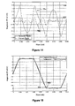
- Figure 9 illustrates, in graph form, a variation in fundamental magnitude against the value of ⁇ 1 for a range of difference values between ⁇ 1 and ⁇ 2 .
- the difference value between ⁇ 1 and ⁇ 2 ranges between 0.2 rad and 0.8 rad. It can be seen from Figure 9 that an increase in the difference value between ⁇ 1 and ⁇ 2 reduces the peak value of the fundamental magnitude.
- Figure 10 illustrates, in graph form, the THD of the AC voltage waveform against the value of ⁇ 1 for the same range of difference values between ⁇ 1 and ⁇ 2 . It can be seen from Figure 10 that an increase in the difference value between ⁇ 1 and ⁇ 2 reduces the THD of the AC voltage waveform but also reduces the achievable fundamental magnitude of the AC voltage waveform.
- the inclusion of the DC side chain-link converters 58 in the voltage source converter provides control over the fundamental magnitude and THD of the AC voltage waveform at the third terminal 42 and permits filtering of a harmonic component from the AC voltage waveform.
- the configuration of the voltage source converter of Figure 2 therefore enables transfer of high quality power between the AC and DC electrical networks 46,44 with reduced or zero filtering requirements.
- the omission of each DC side chain-link converter 58 from the first voltage source converter 30 would result in the problems described earlier with reference to the conventional voltage source converters of Figures 1 a and 1 b.
- control of the configuration of the AC voltage waveform at the third terminal 42 provides control over the voltage experienced by each director switch in each primary limb element portion 38,40 and thereby reduces the risk of damage caused by voltage levels exceeding the voltage ratings of the director switches.
- the director switches can be chosen without having to consider the possibility of voltage levels exceeding the voltage ratings of the director switches.
- the configuration of the voltage source converter of Figure 2 provides savings in terms of its cost, size and footprint as follows.
- the DC side chain-link converters 58 of the secondary limb element portions may be controlled to supply DC current to or absorb DC current from the DC electrical network 44 throughout the power cycle and thereby regulate DC ripple, thus limiting or obviating the need for a DC link capacitor which can be large and costly.
- each primary switching element 50 is a naturally commutated switching element (e.g. a thyristor)
- large snubbing circuitry is normally required to control the rate of change of voltage across each naturally commutated switching element after it has been commutated off.
- large reactors are required to accommodate the long recovery time between the turn-off and turn-on of the primary switching elements 50.
- the inclusion of the DC side chain-link converters 58 however permit fine control of the rate of change of voltage across each naturally commutated switching element and the recovery time between the turn-off and turn-on of each naturally commutated switching element, thus reducing or eliminating the need to include the snubbing circuitry and reactors.
- the configuration of the voltage source converter of Figure 2 therefore results in an economical, space-saving voltage source converter with high voltage capabilities.
- a second voltage source converter 130 according to a second embodiment of the invention is shown in Figure 11 .
- the second voltage source converter 130 of Figure 11 is similar in structure and operation to the first voltage source converter 30 of Figure 2 , and like features share the same reference numerals.
- the second voltage source converter 130 differs from the first voltage source converter 30 in that the second voltage source converter 130 further includes an AC side chain-link converter 74.
- a first end of the AC side chain-link converter 74 is connected to the third terminal 42 of the converter limb 36 of the second voltage source converter 130.
- a second end of the AC side chain-link converter 74 is connected to the AC electrical network 46 via the phase reactance 48.
- Each AC side chain-link converter 74 is similar in structure and operation to each DC side chain-link converter 58.
- control unit 62 controls the switching of the secondary switching elements in each module 60 of the AC side chain-link converter 74 to generate a suitable voltage across the AC side chain-link converter 74 which can be combined with the AC voltage waveform at the third terminal 42 to modify the AC voltage waveform before it is presented to the AC electrical network 46.
- Such modification of the AC voltage waveform can be performed to filter out one or more harmonic components from the AC voltage waveform.
- the AC side chain-link converter 74 therefore provides the voltage source converter with active filtering capability and thereby further reduces or eliminates the requirements for passive filtering at the third terminal 42 of the voltage source converter, thus reducing the real estate requirements of the voltage source converter.
- a third voltage source converter 230 according to a third embodiment of the invention is shown in Figure 12 .
- the third voltage source converter 230 of Figure 12 is similar in structure and operation to the first voltage source converter 30 of Figure 2 , and like features share the same reference numerals.
- the third voltage source converter 230 differs from the first voltage source converter 30 in that, in the third voltage source converter 230:
- each module 60 of each DC side chain-link converter 58 includes two pairs of secondary switching elements and an energy storage device in the form of a capacitor.
- the secondary switching elements are connected in parallel with the capacitor in a full-bridge arrangement to define a 4-quadrant bipolar module 60 that can provide negative, zero or positive voltage and can conduct current in two directions.
- each module 60 is selectively bypassed or inserted into the corresponding DC side chain-link converter 58 by changing the state of the secondary switching elements. This selectively directs current through the capacitor or causes current to bypass the capacitor, so that each module 60 provides a negative, zero or positive voltage.
- each module 60 The capacitor of each module 60 is bypassed when the pairs of secondary switching elements in each module 60 are configured to form a short circuit in the module 60. This causes current in the chain-link converter to pass through the short circuit and bypass the capacitor, and so the module 60 provides a zero voltage, i.e. the module 60 is configured in a bypassed mode.
- each module 60 is inserted into the DC side chain-link converter 58 when the pairs of secondary switching elements in each module 60 are configured to allow the current in the DC side chain-link converter 58 to flow into and out of the capacitor.
- the capacitor then charges or discharges its stored energy so as to provide a non-zero voltage, i.e. the module 60 is configured in a non-bypassed mode.
- the full-bridge arrangement of the secondary switching elements of each module 60 permits configuration of the secondary switching elements to cause current to flow into and out of the capacitor in either direction, and so each module 60 can be configured to provide a negative or positive voltage in the non-bypassed mode.
- the third voltage source converter 230 can be operated to provide a small amount of power to the AC electrical network 46 for, for example, energising auxiliary electronics of a wind farm forming part of the AC electrical network 46 at start-up. This is carried out by the control unit 62 controlling the switching of each secondary switching element in each module 60 of each DC side chain-link converter 58 to control the configuration of the AC voltage waveform at the third terminal 42 such that power is transferred from the third voltage source converter 230 to the AC electrical network 46. Meanwhile, during the provision of power from the third voltage source converter 230 to the AC electrical network 46, each director switch is turned off to keep the corresponding primary limb element portion 38,40 switched out of circuit between the corresponding DC terminal 32,42 and the third terminal 42.
- third voltage source converter 230 can also be operated in a fault operating mode.
- each director switch not only improves the robustness of the primary limb element portions 38,40, but also makes the primary limb element portions 38,40 capable of withstanding the fault current.
- the control unit 62 controls the switching of the secondary switching elements in each module 60 of each DC side chain-link converter 58 to control the voltage at the third terminal 42 to rapidly commutate off each director switch of the corresponding primary limb element portion 38,40 to limit or prevent the fault current, depending on the time taken to achieve the commutation. Commutation of the director switches causes any remaining fault current to be diverted into the DC side chain-link converters 58. Thereafter, the control unit 62 controls the switching of the secondary switching elements in each module 60 of the DC side chain-link converters 58 so that at least one module 60 provides an opposing voltage to block the remaining fault current.
- the use of the voltage source converter components to limit or prevent the fault current reduces or eliminates the need for the installation of separate fault protection equipment. This leads to savings in terms of hardware size, weight and costs.
- Figure 12 shows the configuration of the third voltage source converter 230 as a rectifier.
- each primary switching element 50 may be connected in the opposite direction to enable configuration of the third voltage source converter 230 as an inverter.
- each primary switching element 50 may be replaced by a pair of primary switching elements 50 connected in anti-parallel to form a bidirectional director switch so that each primary limb element portion 38,40 can conduct current in two directions. This allows the third voltage source converter 230 to be configured to transfer power between the AC and DC electrical networks 46,44 in both directions.
- each thyristor may be replaced by another naturally commutated switching device.
- control unit can control the switching of the director switches to form a current bypass path to permit the fault current flowing in the voltage source converter to flow through the current bypass path and thereby bypass the DC side chain-link converters in response to a fault occurring, in use, in the AC or DC electrical network.
- This prevents the fault current from damaging the anti-parallel diodes of the secondary switching elements in each module of the DC side chain-link converters.
- the formation of the current bypass path is particularly useful in a voltage source converter in which each module of each DC side chain-link converter is configured in a half-bridge arrangement (e.g. to define a 2-quadrant unipolar module as shown in Figures 2 and 11 ) instead of a full-bridge arrangement (e.g. to define a 4-quadrant bipolar module as shown in Figure 12 ),
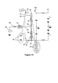
- a fourth voltage source converter 330 according to a fourth embodiment of the invention is shown in Figure 13 .
- the fourth voltage source converter 330 of Figure 13 is similar in structure and operation to the third voltage source converter 230 of Figure 12 , and like features share the same reference numerals.
- the fourth voltage source converter 330 differs from the third voltage source converter 230 in that the fourth voltage source converter 330 further includes an AC side chain-link converter 74, which is similar in structure and operation to each DC side chain-link converter 58 of the third voltage source converter 230.
- a first end of the AC side chain-link converter 74 is connected to the third terminal 42 of the converter limb 36 of the fourth voltage source converter 330.
- a second end of the AC side chain-link converter 74 is connected to the AC electrical network 46 via the phase reactance 48.
- the AC side chain-link converter 74 of the fourth voltage source converter 330 is operated in a similar manner to the AC side chain-link converter 74 of the second voltage source converter 130 to modify the AC voltage waveform before it is presented to the AC electrical network 46.
- a fifth voltage source converter according to a fifth embodiment of the invention is similar in structure and operation to the first voltage source converter 30 of Figure 2 .
- the fifth voltage source converter differs from the first voltage source converter 30 in that the fifth voltage source converter further includes a plurality of converter limbs, the third terminal of each converter limb being connectable to a respective phase of a three-phase AC electrical network.
- the three third terminals of the fifth voltage source converter are connected to the AC electrical network via a star-delta transformer.
- the star-delta transformer is provided with a tap changer to provide control over the fundamental magnitude of each AC voltage waveform at each third terminal.
- the provision of the star-delta transformer to interconnect the fifth voltage source converter and the AC electrical network enables removal of triple N harmonics from each AC voltage waveform before it is presented to the AC electrical network. This thereby reduces the filtering requirements of the fifth voltage source converter.
- the number of converter limbs of the fifth voltage source converter may vary to match the number of phases of a multi-phase AC electrical network to which the fifth voltage source converter is connected.
- a sixth voltage source converter according to a sixth embodiment of the invention is similar in structure and operation to the fifth voltage source converter.
- the sixth voltage source converter differs from the fifth voltage source converter in that the sixth voltage source converter further includes a plurality of AC side chain-link converters.
- a first end of each AC side chain-link converter is connected to the third terminal of a respective one of the converter limbs of the sixth voltage source converter.
- a second end of each AC side chain-link converter is connected to a respective phase of a three-phase AC electrical network.
- the AC side chain-link converters of the sixth voltage source converter are similar in structure and operation to the AC side chain-link converter of the second voltage source converter 130.
- Figure 14 illustrates, in graph form, the super harmonic ripples 76a,76b for the AC voltage waveform, including all super harmonics up to the 19 th harmonic, respectively present at a secondary winding and a primary winding of the transformer if no filtering is carried out by the AC side chain-link converters.
- control unit can control the switching of the secondary switching elements in each module of each AC side chain-link converter to modify the respective AC voltage waveform to follow a voltage locus consisting of only a fundamental component and at least one selected harmonic component of the respective AC voltage waveform.
- Figure 15 compares, in graph form, the AC voltage waveform 80a at one of the third terminals of the sixth voltage source converter with a "filtered" AC voltage waveform 80b which follows a voltage locus consisting of only fundamental and triple N harmonic components of the AC voltage waveform 80a.
- a voltage locus can be used to define the voltage at each secondary winding of the transformer when controlling the voltage of each AC side chain-link converter of the sixth voltage source converter.
Landscapes
- Engineering & Computer Science (AREA)
- Power Engineering (AREA)
- Rectifiers (AREA)
- Inverter Devices (AREA)
- Supply And Distribution Of Alternating Current (AREA)
- Dc-Dc Converters (AREA)
Abstract
Description
- This invention relates to a voltage source converter.
- In power transmission networks alternating current (AC) power is typically converted to direct current (DC) power for transmission via overhead lines and/or under-sea cables. This conversion removes the need to compensate for the AC capacitive load effects imposed by the transmission line or cable, and thereby reduces the cost per kilometer of the lines and/or cables. Conversion from AC to DC thus becomes cost-effective when power needs to be transmitted over a long distance.
- The conversion of AC power to DC power is also utilized in power transmission networks where it is necessary to interconnect the AC electrical networks operating at different frequencies.
- In any such power transmission network, converters are required at each interface between AC and DC power to effect the required conversion, and one such form of converter is a voltage source converter (VSC).
- It is known in voltage source converters to use six-switch (two-level) and three-
level converter topologies Figures 1a and 1b . TheIGBT devices 14 are connected and switched together in series to enable high power ratings of 10's to 100's of MW to be realized. In addition, theIGBT devices 14 switch on and off several times at high voltage over each cycle of the AC supply frequency to control the harmonic currents being fed to the AC electrical network. This leads to high losses, high levels of electromagnetic interference and a complex design. - It is also known in voltage source converters to use a multi-level converter arrangement such as that shown in
Figure 1c . The multi-level converter arrangement includesrespective converter bridges 16 ofcells 18 connected in series. Eachconverter cell 18 includes a pair of series-connected insulated gate bipolar transistors (IGBTs) 20 connected in parallel with acapacitor 22. Theindividual converter cells 18 are not switched simultaneously and the converter voltage steps are comparatively small. Thecapacitor 22 of eachconverter cell 18 is configured to have a sufficiently high capacitive value in order to constrain the voltage variation at the capacitor terminals in such a multi-level converter arrangement, and a high number ofconverter cells 18 are required due to the limited voltage ratings of theIGBTs 20. ADC side reactor 24 is also required in eachconverter bridge 16 to limit transient current flow betweenconverter limbs 26, and thereby enable the parallel connection and operation of theconverter limbs 26. These factors lead to expensive, large and heavy equipment that has significant amounts of stored energy, which makes pre-assembly, testing and transportation of the equipment difficult. - According to an aspect of the invention, there is provided a voltage source converter comprising a converter limb, the converter limb extending between first and second DC terminals and having primary and secondary limb elements connected in parallel between the first and second DC terminals, each DC terminal being connectable to a DC electrical network,
the primary limb element including first and second primary limb element portions separated by a third terminal, the third terminal being connectable to an AC electrical network, each primary limb element portion including at least one primary switching element, each primary switching element being switchable to switch the corresponding primary limb element portion into and out of circuit between a respective one of the DC terminals and the third terminal, the secondary limb element including first and second secondary limb element portions separated by a junction, each secondary limb element portion including a DC side chain-link converter, each chain-link converter including a plurality of series-connected modules, each module of each chain-link converter including at least one secondary switching element and at least one energy storage device, the or each secondary switching element and the or each energy storage device in each module combining to selectively provide a voltage source,
the converter limb further including a connection interconnecting the third terminal and the junction to form a star configuration in which a first branch of the star configuration includes the connection, a second branch of the star configuration includes the first secondary limb element portion, a third branch of the star configuration includes the second secondary limb element portion and the junction defines a mid-point of the star configuration,
wherein the voltage source converter further includes a control unit which controls the switching of each primary switching element to switch the corresponding primary limb element portion into and out of circuit between the corresponding DC terminal and the third terminal to selectively transfer power between the AC and DC electrical networks via each of the primary limb element portions, the control unit further controlling the switching of the or each secondary switching element in each module of each DC side chain-link converter to control the configuration of an AC voltage waveform at the third terminal. - In use, the primary limb element portions provide a primary current path for the transfer of power between the AC and DC electrical networks while the secondary limb element portions, by way of its control of the configuration of the AC voltage waveform at the third terminal, supports the switching of each primary limb element portion into and out of circuit between the corresponding DC terminal and the third terminal.
- The control of the configuration of the AC voltage waveform at the third terminal provides control over the voltage experienced by the or each primary switching element in each primary limb element portion and thereby reduces the risk of damage caused by voltage levels exceeding the voltage ratings of the primary switching elements. As such it is more straightforward to design and optimise the voltage source converter because the primary switching elements can be chosen without having to consider the possibility of voltage levels exceeding the voltage ratings of the primary switching elements.
- In addition the configuration of the voltage source converter according to the invention enables transfer of high quality power between the AC and DC electrical networks with reduced or zero filtering requirements. This is because each of the DC side chain-link converters is capable of providing a stepped variable voltage source, which permits the generation of a voltage waveform across each chain-link converter using a step-wise approximation and thereby formation of a high quality AC voltage waveform at the third terminal. In contrast, the omission of each DC side chain-link converter from the voltage source converter would result in the problems described earlier with reference to the conventional voltage source converters of
Figures 1 a and 1 b. - The configuration of the voltage source converter according to the invention provides savings in terms of its cost, size and footprint as follows.
- During the operation of the voltage source converter, power is divided between the primary and secondary limb elements over each power cycle. By using primary switching elements with low conduction losses in the primary limb element portions, the overall conduction losses in the voltage source converter according to the invention can be reduced in comparison to a conventional voltage source converter having the same number of converter limbs, each converter limb including a plurality of modules, an example of which is shown in
Figure 1c . This provides further savings in terms of the cost, size and footprint of the voltage source converter according to the invention. - The DC side chain-link converters of the secondary limb element portions may be controlled to supply DC current to or absorb DC current from the DC electrical network throughout the power cycle and thereby regulate DC ripple, thus limiting or obviating the need for a DC link capacitor which can be large and costly.
- When each primary switching element is a naturally commutated switching element (e.g. a thyristor), large snubbing circuitry is normally required to control the rate of change of voltage across each naturally commutated switching element after it has been commutated off. Also, large reactors are required to accommodate the long recovery time between the turn-off and turn-on of the primary switching elements. The inclusion of the DC side chain-link converters however permit fine control of the rate of change of voltage across each naturally commutated switching element and the recovery time between the turn-off and turn-on of each naturally commutated switching element, thus reducing or eliminating the need to include the snubbing circuitry and reactors.
- The configuration of the voltage source converter according to the invention therefore results in an economical, space-saving voltage source converter with high voltage capabilities.
- In embodiments of the invention the control unit, while both primary limb element portions are switched out of circuit between the respective DC terminal and the third terminal, may control the switching of the or each secondary switching element in each module of each DC side chain-link converter to control the rate of change of voltage at the third terminal. In other words, the control unit may control the switching of the or each secondary switching element in each module of each DC side chain-link converter to control the rate of change of voltage at the third terminal in the period which follows the switching of one of the primary limb element portions out of circuit between the corresponding DC terminal and the third terminal and precedes the switching of the other of the primary limb element portions into circuit between the corresponding DC terminal and the third terminal. Preferably such switching of the or each secondary switching element in each module of each DC side chain-link converter results in the formation of a substantially trapezoidal voltage waveform at the third terminal.
- The capability of the DC side chain-link converters to provide a stepped variable voltage source permits fine control over the rate of change of voltage at the third terminal to prevent the voltage from ramping too quickly between different voltage levels, thereby avoiding the occurrence of fast fronted and high voltage spikes that may otherwise damage or degrade components or their insulation.
- The control unit, while both primary limb element portions are switched out of circuit between the respective DC terminal and the third terminal, may control the switching of the or each secondary switching element in each module of each DC side chain-link converter to control the rate of change of voltage at the third terminal to modify the characteristics of the overall AC voltage waveform at the third terminal.
- Optionally, the control unit may control the switching of the or each secondary switching element in each module of the DC side chain-link converter to modify the value of each intercept angle of the AC voltage waveform to control the fundamental magnitude of the AC voltage waveform.
- Further optionally, the control unit may control the switching of the or each secondary switching element in each module of the DC side chain-link converter to modify the value of each intercept angle of the AC voltage waveform to filter a harmonic component from the AC voltage waveform.
- For the purposes of the specification, an intercept angle is defined as a phase angle corresponding to a common point of intersection between two different voltage slopes of the AC voltage waveform, whereby a voltage slope has a constant rate of change of voltage (which can be negative, zero or positive).
- Simple harmonic analysis shows that, as the magnitude of each intercept angle increases, the overall harmonic content of the AC voltage waveform reduces to a minima at 0.61 rad which is close to the point where the 5th harmonic passes through zero at 0.628 rad. The simple harmonic analysis also shows that the overall harmonic content of the AC voltage waveform rises as the magnitude of each intercept angle further increases beyond 0.628 rad. It follows that, when the voltage source converter is controlled to filter a harmonic component from the AC voltage waveform, the magnitude of each intercept angle is preferably 0.61 rad, 0.628 rad or in the range of 0.61 to 0.628 rad.
- It will be noted that the fundamental magnitude of the AC voltage waveform does not vary significantly with the magnitude of each intercept angle. As such, in order to obtain a certain level of operation expected of the voltage source converter, a transformer with a tap changer may be used in combination with a small variation in fundamental magnitude over a selected range to give continuous control over the tap steps.
- Alternatively, in order to obtain a certain level of operation expected of the voltage source converter, the AC voltage waveform may be controlled to include a voltage plateau about the phase angle corresponding to zero voltage. To obtain such an AC voltage waveform, the control unit, while both primary limb element portions are switched out of circuit between the respective DC terminal and the third terminal, may control the switching of the or each secondary switching element in each module of each DC side chain-link converter to generate a voltage plateau which is symmetrical about a phase angle n·(π + ϕ) of the AC voltage waveform at the third terminal, where n is an integer and ϕ is a phase shift between a first vector representing an AC voltage of the AC electrical network and a second vector representing the AC voltage waveform at the third terminal. The addition of such a voltage plateau to the AC voltage waveform not only provides control over the fundamental magnitude of the AC voltage waveform, but also permits reduction of the Total Harmonic Distortion (THD) of the AC voltage waveform.
- In embodiments of the invention the control unit, prior to one of the primary limb element portions being switched into or out of circuit between the corresponding DC terminal and the third terminal, may control the switching of the or each secondary switching element in each module of each DC side chain-link converter to control the configuration of the AC voltage waveform at the third terminal to minimise a voltage across that primary limb element portion. This allows the or each primary switching element of that limb portion to be switched at near zero voltage and current, thus minimise switching losses.
- In further embodiments of the invention the voltage source converter may further include an AC side chain-link converter, a first end of the AC side chain-link converter being connected to the third terminal and a second end of the AC side chain-link converter being connectable to the AC electrical network, the control unit controlling the switching of the or each secondary switching element in each module of the AC side chain-link converter to modify the AC voltage waveform for presentation to the AC electrical network.
- It is standard practice to include passive filters at the output of power converters. However, for a grid-connected converter, the inclusion of passive filters has a sever effect on the quadrature termination impedance of the converter. Thus, the passive filters are typically switched, using switchgear, in and out of circuit with the converter in accordance with load conditions. The inclusion of the passive filters and switchgear contributes to the majority of the real estate requirements of an associated power station.
- On the other hand the AC side chain-link converter provides the voltage source converter with active filtering capability and thereby further reduces or eliminates the requirements for passive filtering at the third terminal of the voltage source converter, thus reducing the real estate requirements of the voltage source converter.
- In embodiments employing the use of an AC side chain-link converter the control unit may control the switching of the or each secondary switching element in each module of the AC side chain-link converter to modify the AC voltage waveform to follow a voltage locus consisting of only a fundamental component and at least one selected harmonic component of the AC voltage waveform. This permits simplification of the control scheme for the AC side chain-link converter because otherwise it would be necessary to perform a complicated harmonic analysis of the AC voltage waveform to separate out the or each unwanted harmonic component.
- Each energy storage device may be any device that is capable of storing or releasing energy, e.g. a capacitor or battery. Each energy storage device must be rated to account for the rise or fall in voltage level caused by the combination of AC and DC currents in each DC side chain-link converter during its operation to control the configuration of the AC voltage waveform at the third terminal. A rise or fall in voltage level of each energy storage device may also occur as a result of the control of each DC side chain-link converter to balance the voltage levels of its energy storage devices.
- Each DC side chain-link converter may be controlled to correct for any net variation in energy due to a rise or fall in energy level of each DC side chain-link converter when both primary limb element portions are respectively switched out of circuit between the corresponding DC terminal and the third terminal to maintain a specific voltage level of each of its energy storage devices. For example, the control unit may control the switching of the or each secondary switching element in each module of each DC side chain-link converter to discharge surplus energy from the DC side chain-link converter of the first secondary limb element portion or inject energy from the DC electrical network into the DC side chain-link converter of the first secondary limb element portion while the first primary limb element portion is not in conduction and the second primary limb element portion is in conduction and to discharge surplus energy from the DC side chain-link converter of the second secondary limb element portion or inject energy from the DC electrical network into the DC side chain-link converter of the second secondary limb element portion while the second primary limb element portion is not in conduction and the first primary limb element portion is in conduction.
- Each module may be a unidirectional voltage source that can provide zero or non-zero voltage and can conduct current in two directions, i.e. each module may be a 2-quadrant unipolar module. For example, each module may include a pair of secondary switching elements connected in parallel with an energy storage device in a half-bridge arrangement to define a 2-quadrant unipolar module that can provide zero or positive voltage and can conduct current in two directions.
- Each module may be a bidirectional voltage source that can provide negative, zero or positive voltage and can conduct current in two directions, i.e. each module may be a 4-quadrant bipolar module. For example, each module may include two pairs of secondary switching elements connected in parallel with an energy storage device in a full-bridge arrangement to define a 4-quadrant bipolar module that can provide negative, zero or positive voltage and can conduct current in two directions.
- The modular arrangement of each chain-link converter means that it is straightforward to increase or decrease the number of modules in each chain-link converter to achieve a desired voltage rating or filtering capability.
- Each primary switching element may be a self-commutated switching element such as, for example, an insulated gate bipolar transistor, a gate turn-off thyristor, a field effect transistor, an injection-enhanced gate transistor or an integrated gate commutated thyristor.
- Each primary switching element may be a naturally commutated switching element such as, for example, a thyristor or a diode. The use of at least one naturally-commutated switching device in each primary limb element portion not only improves the robustness of the primary limb element portions, but also makes the primary limb element portions capable of withstanding surge currents that might occur due to faults in the DC electrical network. In such embodiments employing the use of naturally commutated switching elements as the primary switching elements, each module of each DC side chain-link converter is preferably a 4-quadrant bipolar module which can be switched to block the aforementioned surge currents.
- It will be understood that the control unit can control the switching of each primary switching element either by sending a turn-on or turn-off control signal to each primary switching element or by controlling the switching of the or each secondary switching element in each module of each DC side chain-link converter to control the configuration of the AC voltage waveform of the third terminal to selectively cause switching of each primary switching element, depending on the type of primary switching element used.
- The configuration of the voltage source converter according to the invention permits simplification of the design and construction of the primary limb element portions without adversely affecting the performance of the voltage source converter according to the invention. For example, each primary limb element portion may include a single primary switching element or a plurality of primary switching elements connected in series between the corresponding DC terminal and the third terminal. Switching elements with high voltage ratings can be selected for use in the primary limb element portions to further reduce the footprint of the voltage source converter and thereby minimise the real estate costs of the associated power station.
- In embodiments of the invention, the control unit may control the switching of the or each secondary switching element in each module of each DC side chain-link converter to control the configuration of the AC voltage waveform at the third terminal to selectively transfer power from the voltage source converter to the AC electrical network. This enables the voltage source converter to provide a small amount of power to the AC electrical network for, for example, energising auxiliary electronics of a wind farm forming part of the AC electrical network at start-up, thus omitting the need for additional equipment to energise the auxiliary electronics.
- Optionally, when each primary switching element is a naturally commutated switching element, the control unit may control the switching of the or each secondary switching element in each module of each DC side chain-link converter to control the configuration of the AC voltage waveform at the third terminal to selectively commutate each primary switching element in response to a fault occurring, in use, in the AC or DC electrical network.
- In the event of a fault occurring, in use, in the AC or DC electrical network, each DC side chain-link converter can be controlled to rapidly commutate off the or each primary switching element of the corresponding primary limb element portion to limit or prevent the fault current, depending on the time taken to achieve the commutation.
- Further optionally, the control unit may control the switching of the or each primary switching element to form a current bypass path to permit a current flowing in the voltage source converter to flow through the current bypass path and thereby bypass each DC side chain-link converter in response to a fault occurring, in use, in the AC or DC electrical network. This prevents the fault current from damaging the components of each module of each DC side chain-link converter.
- Thus, the use of the voltage source converter components to limit or prevent the fault current reduces or eliminates the need for the installation of separate fault protection equipment. This leads to savings in terms of hardware size, weight and costs.
- Optionally each primary limb element portion may include at least one pair of primary switching elements connected in anti-parallel so that each primary limb element portion can conduct current in two directions. This allows the voltage source converter to be configured to transfer power between the AC and DC electrical networks in both directions. Each primary switching element of the or each pair of primary switching elements may include a single switching device or a plurality of series and/or parallel-connected switching devices.
- The voltage source converter may be a multi-phase voltage source converter. In embodiments of the invention in which the voltage source converter is connectable to a multi-phase AC electrical network, the voltage source converter may include a plurality of converter limbs, the third terminal of each converter limb being connectable to a respective phase of a multi-phase AC electrical network.
- Preferred embodiments of the invention will now be described, by way of example only, with reference to the accompanying drawings in which:
-
Figures 1a, 1b and1c show, in schematic form, prior art voltage source converters; -
Figure 2 shows, in schematic form, a voltage source converter according to a first embodiment of the invention; -
Figure 3 illustrates, in graph form, an AC voltage waveform generated, in use, at a third terminal of the voltage source converter ofFigure 2 ; -
Figure 4 shows, in schematic form, the combination of AC and DC currents in each DC side chain-link converter during its operation to control the configuration of the AC voltage waveform at the third terminal of the voltage source converter ofFigure 2 ; -
Figure 5 illustrates, in graph form, the charging and discharging of each capacitor in the DC side chain-link converters of the first and second secondary limb element portions during the operation of the voltage source converter ofFigure 2 as a rectifier; -
Figure 6 illustrates, in graph form, a variation in harmonic amplitude of the fundamental and non-triple N harmonic components of the AC voltage waveform for a range of values for an intercept angle α; -
Figure 7 which illustrates, in graph form, a frequency analysis of the AC phase current at the third terminal of the voltage source converter ofFigure 2 for an intercept angle α of 0.628 rad; -
Figure 8 illustrates, in graph form, another AC voltage waveform generated, in use, at a third terminal of the voltage source converter ofFigure 2 in which the AC voltage waveform includes a voltage plateau between -α1 and +α1 for controlling its fundamental magnitude; -
Figure 9 illustrates, in graph form, a variation in fundamental magnitude against α1 for a range of difference values between different intercept angles, α1 and α2; -
Figure 10 illustrates, in graph form, the total harmonic distortion (THD) of the AC voltage waveform against α1 for a range of difference values between different intercept angles α1 and α2. -
Figure 11 shows, in schematic form, a voltage source converter according to a second embodiment of the invention; -
Figure 12 shows, in schematic form, a voltage source converter according to a third embodiment of the invention; -
Figure 13 shows, in schematic form, a voltage source converter according to a fourth embodiment of the invention; -
Figure 14 illustrates, in graph form, a super harmonic ripples for an unfiltered AC voltage waveform, including all super harmonics up to the 19th harmonic, respectively present at a secondary winding and a primary winding of a star-delta transformer; and -
Figure 15 compares, in graph form, the AC voltage waveform at a third terminal of a voltage source converter with a "filtered" AC voltage waveform which follows a voltage locus consisting of only fundamental and triple N harmonic components of the AC voltage waveform. - A first
voltage source converter 30 according to a first embodiment of the invention is shown inFigure 2 . - The first
voltage source converter 30 comprises first andsecond DC terminals converter limb 36. - The
converter limb 36 extends between the first andsecond DC terminals second DC terminals - The primary limb element includes first and second primary
limb element portions third terminal 42. In other words, the first primarylimb element portion 38 is connected between thefirst DC terminal 32 and thethird terminal 42, and the second primarylimb element portion 40 is connected between thesecond DC terminal 34 and thethird terminal 42. - In use, the first and
second DC terminals electrical network 44, the positive and negative terminals of the DCelectrical network 44 carrying voltages of +Vdc and -Vdc respectively, and thethird terminal 42 is connected to an ACelectrical network 46 via aphase reactance 48, - Each primary limb element portion includes a director switch, which includes a plurality of series-connected
primary switching elements 50. Eachprimary switching element 50 is in the form of an insulated gate bipolar transistor (IGBT) which is connected in parallel with an anti-parallel diode. It is envisaged that, in other embodiments of the invention, each IGBT may be replaced by a gate turn-off thyristor, a field effect transistor, an injection-enhanced gate transistor, an integrated gate commutated thyristor or any other self-commutated semiconductor device. - It is further envisaged that, in other embodiments of the invention, each plurality of series-connected
primary switching elements 50 may be replaced by a singleprimary switching element 50. - The configuration of the primary
limb element portions primary switching element 50 is switchable to switch the corresponding primarylimb element portion third terminal 42. - The secondary limb element includes first and second secondary
limb element portions junction 56. In other words, the first secondarylimb element portion 52 is connected between thefirst DC terminal 32 and thejunction 56, and the second secondarylimb element portion 54 is connected between thesecond DC terminal 34 and thejunction 56. - Each secondary limb element portion includes a DC side chain-
link converter 58. Each DC side chain-link converter 58 includes a plurality of series-connectedmodules 60. Eachmodule 60 includes a pair of secondary switching elements and an energy storage device in the form of a capacitor. The secondary switching elements are connected in parallel with the capacitor in a half-bridge arrangement to define a 2-quadrantunipolar module 60 that can provide zero or positive voltage and can conduct current in two directions. - Each secondary switching element is constituted by a semiconductor device in the form of an Insulated Gate Bipolar Transistor (IGBT) which is connected in parallel with an anti-parallel diode. It is envisaged that, in other embodiments of the invention, each secondary switching element may be a different switching device such as a gate turn-off thyristor, a field effect transistor, an injection-enhanced gate transistor, an integrated gate commutated thyristor or any other self-commutated semiconductor device.
- It is envisaged that, in other embodiments of the invention, the capacitor may be replaced by another energy storage device that is capable of storing or releasing energy, e.g. a battery.
- The capacitor of each
module 60 is selectively bypassed or inserted into the corresponding DC side chain-link converter 58 by changing the state of the secondary switching elements. This selectively directs current through the capacitor or causes current to bypass the capacitor, so that eachmodule 60 provides a zero or positive voltage. - The capacitor of each
module 60 is bypassed when the pair of secondary switching elements in eachmodule 60 is configured to form a short circuit in themodule 60. This causes current in the DC side chain-link converter 58 to pass through the short circuit and bypass the capacitor, and so themodule 60 provides a zero voltage, i.e. themodule 60 is configured in a bypassed mode. - The capacitor of each
module 60 is inserted into the DC side chain-link converter 58 when the pair of secondary switching elements in eachmodule 60 is configured to allow the current in the DC side chain-link converter 58 to flow into and out of the capacitor. The capacitor then charges or discharges its stored energy so as to provide a positive voltage, i.e. themodule 60 is configured in a non-bypassed mode. - It is possible to build up a combined voltage across each DC side chain-
link converter 58, which is higher than the voltage available from each of itsindividual modules 60, via the insertion of the capacitors ofmultiple modules 60, each providing its own voltage, into each DC side chain-link converter 58. In this manner switching of the secondary switching elements of eachmodule 60 causes each DC side chain-link converter 58 to provide a stepped variable voltage source, which permits the generation of a voltage waveform across each DC side chain-link converter 58 using a step-wise approximation. - The
converter limb 36 further includes a connection interconnecting thethird terminal 42 and thejunction 56 to form a star configuration in which a first branch of the star configuration includes the connection, a second branch of the star configuration includes the first secondarylimb element portion 52, a third branch of the star configuration includes the second secondarylimb element portion 54 and thejunction 56 defines a mid-point of the star configuration. The connection interconnecting thethird terminal 42 and thejunction 56 allows the DC side chain-link converters 58 to be operated to control the configuration of an AC voltage waveform at thethird terminal 42. - The voltage source converter further includes a
control unit 62 to control the switching of the director switches in the primarylimb element portions module 60 of each DC side chain-link converter 58. - Operation of the voltage source converter of
Figure 2 is described as follows, with reference toFigure 3 . - In order to transfer power between the AC and DC
electrical networks control unit 62 controls the director switches to switch the primary limb portions into and out of circuit between the respective DC terminal and the third terminal 42 to provide a current path between the AC and DCelectrical networks - During the operation of the voltage source converter, the peak AC voltage of the AC
electrical network 46 is slightly lower than the DC voltage of the DCelectrical network 44. - For the purposes of describing how the voltage source converter works, it is assumed that the starting point of the operation of the voltage source converter is the point at which the
control unit 62 turns on the director switch of the second primarylimb element portion 40 and thereby switches the second primarylimb element portion 40 into circuit between thesecond DC terminal 34 and thethird terminal 42. It will be appreciated that the starting point of the operation of the voltage source converter can differ depending on the requirements of the power application associated with the voltage source converter. - When the second primary
limb element portion 40 is switched into circuit between thesecond DC terminal 34 and the third terminal 42 (as indicated by 66a inFigure 3 ), the director switch in the second primarylimb element portion 40 is closed while the director switch in the first primarylimb element portion 38 is open. Current is prevented from flowing into the first primarylimb element portion 38 as a result of the anti-parallel diodes of the first primarylimb element portion 38 being reverse-biased. The switching of the second primarylimb element portion 40 into circuit provides a current path that connects thesecond DC terminal 34 to thethird terminal 42 and thereby results in a voltage of - VDC being presented at thethird terminal 42. - After a certain period of time, the
control unit 62 turns off the director switch of the second primarylimb element portion 40. Since thesecond DC terminal 34 and the third terminal 42 at this stage share the same voltage of -VDC, the voltage across the second primarylimb element portion 40 is near zero voltage and current. This thereby allows the director switch of the second primarylimb element portion 40 to be turned off at near zero voltage and current, thus minimising switching losses. At the same time thecontrol unit 62 controls the switching of the secondary switching elements in eachmodule 60 of the DC side chain-link converters 58 to present a voltage of +VDC at the third terminal 42 which is now disconnected from thesecond DC terminal 34 as a result of the director switch of the second primarylimb element portion 40 being turned off and the anti-parallel diodes of the second primarylimb element portion 40 being reverse-biased. - The
control unit 62 then controls the switching of the secondary switching elements in eachmodule 60 of the DC side chain-link converters 58 to ramp the voltage at the third terminal 42 in a positive direction (as indicated by 66b inFigure 3 ). The anti-parallel diodes of the first and second primarylimb element portions limb element portions - When the voltage at the
third terminal 42 reaches +VDC, thecontrol unit 62 turns on the director switch of the first primarylimb element portion 38 and thereby switches the first primarylimb element portion 38 into circuit between thefirst DC terminal 32 and the third terminal 42 (as indicated by 66c inFigure 3 ). Since thefirst DC terminal 32 and the third terminal 42 at this stage share the same voltage of +VDC, the switching of the director switch of the first primarylimb element portion 38 occurs at near zero voltage and current, thus minimising switching losses. Current is prevented from flowing into the second primarylimb element portion 40 as a result of the anti-parallel diodes of the second primarylimb element portion 40 being reverse-biased. The switching of the first primarylimb element portion 38 into circuit provides a current path that connects thefirst DC terminal 32 to thethird terminal 42 and thereby results in a voltage of +VDC being presented at thethird terminal 42. - After a certain period of time, the
control unit 62 turns off the director switch of the first primarylimb element portion 38 and controls the switching of the secondary switching elements in eachmodule 60 of the DC side chain-link converters 58 to present a voltage of +VDC at the third terminal 42 which is now disconnected from thefirst DC terminal 32 as a result of the director switch of the first primarylimb element portion 38 being turned off and the anti-parallel diodes of the first primarylimb element portion 38 being reverse-biased. Thecontrol unit 62 then controls the switching of the secondary switching elements in eachmodule 60 of the DC side chain-link converters 58 to ramp the voltage at the third terminal 42 in a negative direction until the voltage at thethird terminal 42 reaches -VDC. Thereafter, thecontrol unit 62 turns on the director switch of the second primarylimb element portion 40 to switch the second primarylimb element portion 40 back into circuit between thesecond DC terminal 34 and the third terminal 42 (as indicated by 66a inFigure 3 ). - Switching the first and second primary
limb element portions third terminal 42. - In this manner the voltage source converter is able to carry out a power transfer function in which the primary
limb element portions electrical networks third terminal 42, supports the switching of each primarylimb element portion third terminal 42. - Each capacitor must be rated to account for the variation in voltage level caused by the combination of AC and DC currents in each DC side chain-
link converter 58, as shown inFigure 4 , during its operation to control the configuration of the AC voltage waveform at thethird terminal 42. In particular, the flow of AC current in the secondary limb element results in near-cancellation of the AC and DC currents in one DC side chain-link converter 58 and summation of the AC and DC currents in the other DC side chain-link converter 58. - A rise in voltage level of each capacitor may also occur as a result of the control of each DC side chain-
link converter 58 to balance the voltage levels of its capacitors. - During the operation of the voltage source converter, the
control unit 62 may control the switching of the secondary switching elements in eachmodule 60 of each DC side chain-link converter 58 to correct for any net variation in energy in each DC side chain-link converter 58, an example of which is shown inFigure 5 . -
Figure 5 illustrates, in graph form, the charging and discharging of each capacitor in the DC side chain-link converters 58 of the first and second secondarylimb element portions voltage source converter 30 as a rectifier. - Surplus energy is absorbed by the DC side chain-
link converter 58 of the first secondarylimb element portion 52 in the periods in which both primarylimb element portions corresponding DC terminal third terminal 42. This surplus energy is then discharged into the DCelectrical network 44 from the DC side chain-link converter 58 of the first secondarylimb element portion 52 in the period in which the first primarylimb element portion 38 is not in conduction and the second primarylimb element portion 40 is in conduction (as indicated by 68a inFigure 5 ). This is because, while the first primarylimb element portion 38 is in conduction, there is insufficient voltage across the DC side chain-link converter 58 of the first secondarylimb element portion 52 to permit discharge of its surplus energy. - Surplus energy is also absorbed by the DC side chain-
link converter 58 of the second secondarylimb element portion 54 in the periods in which both primarylimb element portions corresponding DC terminal third terminal 42. This surplus energy is then discharged into the DCelectrical network 44 from the DC side chain-link converter 58 of the second secondarylimb element portion 54 in the period in which the second primarylimb element portion 40 is not in conduction and the first primarylimb element portion 38 is in conduction (as indicated by 68b inFigure 5 ). This is because, while the second primarylimb element portion 40 is in conduction, there is insufficient voltage across the DC side chain-link converter 58 of the second secondarylimb element portion 54 to permit discharge of its surplus energy. - When the first
voltage source converter 30 is operated as an inverter, the energy level of each DC side chain-link converter 58 falls in the period in which both primarylimb element portions corresponding DC terminal third terminal 42. - To minimise the net variation in energy level charge in the DC side chain-
link converter 58 of the first secondarylimb element portion 52, the control unit controls the switching of the secondary switching elements in eachmodule 60 of each DC side chain-link converter 58 such that energy from the DCelectrical network 44 is injected into the DC side chain-link converter 58 of the first secondarylimb element portion 52 in the period in which the first primarylimb element portion 38 is not in conduction and the second primarylimb element portion 40 is in conduction. This is because, while the first primarylimb element portion 38 is in conduction, there is insufficient voltage across the DC side chain-link converter 58 of the first secondarylimb element portion 52 to permit injection of energy from the DCelectrical network 44. - To minimise the net variation in energy level charge in the DC side chain-
link converter 58 of the second secondarylimb element portion 54, the control unit controls the switching of the secondary switching elements in eachmodule 60 of each DC side chain-link converter 58 such that energy from the DCelectrical network 44 is injected into the DC side chain-link converter 58 of the second secondarylimb element portion 54 in the period in which the second primarylimb element portion 40 is not in conduction and the first primarylimb element portion 38 is in conduction. This is because, while the second primarylimb element portion 40 is in conduction, there is insufficient voltage across the DC side chain-link converter 58 of the second secondarylimb element portion 54 to permit injection of energy from the DCelectrical network 44. - The use of the DC side chain-
link converters 58 to control the rate of change of voltage at thethird terminal 42 prevents the voltage at the third terminal 42 from ramping too quickly between +VDC and -VDC. Using the DC side chain-link converters 58 to control the ramp of the voltage from +VDC and -VDC results in a trapezoidal waveform, as shown inFigure 3 , which prevents the occurrence of fast and high voltage spikes which affect the design and rating of the switching elements. - In addition the rate of change of voltage at the
third terminal 42 can be adjusted to modify the characteristics of the overall AC voltage waveform at the third terminal 42 in order to control the fundamental magnitude of the AC voltage waveform and/or filter a harmonic component from the AC voltage waveform. -
Figure 6 illustrates, in graph form, a variation in harmonic amplitude of the fundamental and non-triple N harmonic components of the AC voltage waveform for a range of values for an intercept angle α. For the purposes of the specification, an intercept angle α,-α is defined as a phase angle which corresponds to a common point of intersection between two different voltage slopes of the AC voltage waveform, whereby a voltage slope has a constant rate of change of voltage (which can be negative, zero or positive). As shown inFigure 3 , each common point of intersection is formed at each phase angle α,-α at which each primarylimb element portion third terminal 42. - The
control unit 62 may be controlled to modify each intercept angle α,-α by adjusting the length of the period in which each primarylimb element portion third terminal 42. - It can be seen from
Figure 6 that increasing the intercept angle α,-α reduces the fundamental magnitude of the AC voltage waveform. - It can be also seen from
Figure 6 that the intercept angle α,-α can be set to reduce the harmonic amplitude of a harmonic component. For example, the 5th harmonic of the AC voltage waveform can be reduced to zero by setting α to be equal to 0.6283 rad (as indicated by 70 inFigure 6 ). The reduction in the 5th harmonic of the AC voltage waveform is shown inFigure 7 which illustrates, in graph form, a frequency analysis of the AC phase current at thethird terminal 42. - Furthermore the
control unit 62, while both primarylimb element portions third terminal 42, can control the switching of the secondary switching elements in eachmodule 60 of each DC side chain-link converter 58 to generate avoltage plateau 72a, as shown inFigure 8 . In particular, while both primarylimb element portions third terminal 42, thecontrol unit 62 controls the switching of the secondary switching elements in eachmodule 60 of the DC side chain-link converters 58 to first carry out avoltage ramp 72b until the voltage reaches avoltage plateau 72a (which is at zero voltage in this case), maintaining thevoltage plateau 72a for a certain period of time and then finally carrying out anothervoltage ramp 72c. Thevoltage plateau 72a is configured to be symmetrical about a phase angle n·π of the AC voltage waveform, where n is an integer. - Therefore, a first common point of intersection is formed at each phase angle α1,-α1 at which each
voltage ramp voltage plateau 72a, and a second common point of intersection is formed at each phase angle α2,-α2 at which each primarylimb element portion third terminal 42. - The
control unit 62 may be controlled to modify each intercept angle α1,-α1,α2,-α2 by adjusting the length of the period in which each primarylimb element portion third terminal 42 and by adjusting the length of the period in which thevoltage plateau 72a is maintained. -
Figure 9 illustrates, in graph form, a variation in fundamental magnitude against the value of α1 for a range of difference values between α1 and α2. The difference value between α1 and α2 ranges between 0.2 rad and 0.8 rad. It can be seen fromFigure 9 that an increase in the difference value between α1 and α2 reduces the peak value of the fundamental magnitude. -
Figure 10 illustrates, in graph form, the THD of the AC voltage waveform against the value of α1 for the same range of difference values between α1 and α2. It can be seen fromFigure 10 that an increase in the difference value between α1 and α2 reduces the THD of the AC voltage waveform but also reduces the achievable fundamental magnitude of the AC voltage waveform. - The addition of the
aforementioned voltage plateau 72a to the AC voltage waveform therefore not only provides control over the fundamental magnitude of the AC voltage waveform, but also permits reduction of the THD of the AC voltage waveform. - As such the inclusion of the DC side chain-
link converters 58 in the voltage source converter provides control over the fundamental magnitude and THD of the AC voltage waveform at thethird terminal 42 and permits filtering of a harmonic component from the AC voltage waveform. The configuration of the voltage source converter ofFigure 2 therefore enables transfer of high quality power between the AC and DCelectrical networks link converter 58 from the firstvoltage source converter 30 would result in the problems described earlier with reference to the conventional voltage source converters ofFigures 1 a and 1 b. - Furthermore the control of the configuration of the AC voltage waveform at the
third terminal 42 provides control over the voltage experienced by each director switch in each primarylimb element portion - The configuration of the voltage source converter of
Figure 2 provides savings in terms of its cost, size and footprint as follows. - During the operation of the voltage source converter, power is divided between the primary and secondary limb elements over each power cycle. By using
primary switching elements 50 with low conduction losses in the primarylimb element portions Figure 1c . This provides further savings in terms of the cost, size and footprint of the voltage source converter according to the invention. - The DC side chain-
link converters 58 of the secondary limb element portions may be controlled to supply DC current to or absorb DC current from the DCelectrical network 44 throughout the power cycle and thereby regulate DC ripple, thus limiting or obviating the need for a DC link capacitor which can be large and costly. - When each
primary switching element 50 is a naturally commutated switching element (e.g. a thyristor), large snubbing circuitry is normally required to control the rate of change of voltage across each naturally commutated switching element after it has been commutated off. Also, large reactors are required to accommodate the long recovery time between the turn-off and turn-on of theprimary switching elements 50. The inclusion of the DC side chain-link converters 58 however permit fine control of the rate of change of voltage across each naturally commutated switching element and the recovery time between the turn-off and turn-on of each naturally commutated switching element, thus reducing or eliminating the need to include the snubbing circuitry and reactors. - The configuration of the voltage source converter of
Figure 2 therefore results in an economical, space-saving voltage source converter with high voltage capabilities. - A second
voltage source converter 130 according to a second embodiment of the invention is shown inFigure 11 . The secondvoltage source converter 130 ofFigure 11 is similar in structure and operation to the firstvoltage source converter 30 ofFigure 2 , and like features share the same reference numerals. - The second
voltage source converter 130 differs from the firstvoltage source converter 30 in that the secondvoltage source converter 130 further includes an AC side chain-link converter 74. A first end of the AC side chain-link converter 74 is connected to thethird terminal 42 of theconverter limb 36 of the secondvoltage source converter 130. In use, a second end of the AC side chain-link converter 74 is connected to the ACelectrical network 46 via thephase reactance 48. - Each AC side chain-
link converter 74 is similar in structure and operation to each DC side chain-link converter 58. - In use, the
control unit 62 controls the switching of the secondary switching elements in eachmodule 60 of the AC side chain-link converter 74 to generate a suitable voltage across the AC side chain-link converter 74 which can be combined with the AC voltage waveform at the third terminal 42 to modify the AC voltage waveform before it is presented to the ACelectrical network 46. Such modification of the AC voltage waveform can be performed to filter out one or more harmonic components from the AC voltage waveform. - The AC side chain-
link converter 74 therefore provides the voltage source converter with active filtering capability and thereby further reduces or eliminates the requirements for passive filtering at thethird terminal 42 of the voltage source converter, thus reducing the real estate requirements of the voltage source converter. - A third
voltage source converter 230 according to a third embodiment of the invention is shown inFigure 12 . The thirdvoltage source converter 230 ofFigure 12 is similar in structure and operation to the firstvoltage source converter 30 ofFigure 2 , and like features share the same reference numerals. - The third
voltage source converter 230 differs from the firstvoltage source converter 30 in that, in the third voltage source converter 230: - each
primary switching element 50 is in the form of a thyristor instead of an IGBT connected in parallel with an anti-parallel diode; - turn-off of each director switch is carried out by the
control unit 62 controlling the switching of the secondary switching elements in eachmodule 60 of each DC side chain-link converter 58 to control the configuration of the AC voltage waveform of the third terminal 42 to commutate off the director switch; - each
module 60 of each DC side chain-link converter 58 is a 4-quadrantbipolar module 60 instead of a 2-quadrantunipolar module 60. - More specifically each
module 60 of each DC side chain-link converter 58 includes two pairs of secondary switching elements and an energy storage device in the form of a capacitor. The secondary switching elements are connected in parallel with the capacitor in a full-bridge arrangement to define a 4-quadrantbipolar module 60 that can provide negative, zero or positive voltage and can conduct current in two directions. - The capacitor of each
module 60 is selectively bypassed or inserted into the corresponding DC side chain-link converter 58 by changing the state of the secondary switching elements. This selectively directs current through the capacitor or causes current to bypass the capacitor, so that eachmodule 60 provides a negative, zero or positive voltage. - The capacitor of each
module 60 is bypassed when the pairs of secondary switching elements in eachmodule 60 are configured to form a short circuit in themodule 60. This causes current in the chain-link converter to pass through the short circuit and bypass the capacitor, and so themodule 60 provides a zero voltage, i.e. themodule 60 is configured in a bypassed mode. - The capacitor of each
module 60 is inserted into the DC side chain-link converter 58 when the pairs of secondary switching elements in eachmodule 60 are configured to allow the current in the DC side chain-link converter 58 to flow into and out of the capacitor. The capacitor then charges or discharges its stored energy so as to provide a non-zero voltage, i.e. themodule 60 is configured in a non-bypassed mode. The full-bridge arrangement of the secondary switching elements of eachmodule 60 permits configuration of the secondary switching elements to cause current to flow into and out of the capacitor in either direction, and so eachmodule 60 can be configured to provide a negative or positive voltage in the non-bypassed mode. - In addition to the operation of the third
voltage source converter 230 to transfer power between the AC and DCelectrical networks voltage source converter 230 can be operated to provide a small amount of power to the ACelectrical network 46 for, for example, energising auxiliary electronics of a wind farm forming part of the ACelectrical network 46 at start-up. This is carried out by thecontrol unit 62 controlling the switching of each secondary switching element in eachmodule 60 of each DC side chain-link converter 58 to control the configuration of the AC voltage waveform at the third terminal 42 such that power is transferred from the thirdvoltage source converter 230 to the ACelectrical network 46. Meanwhile, during the provision of power from the thirdvoltage source converter 230 to the ACelectrical network 46, each director switch is turned off to keep the corresponding primarylimb element portion corresponding DC terminal third terminal 42. - Furthermore the third
voltage source converter 230 can also be operated in a fault operating mode. - After a fault occurs in the AC or DC
electrical network voltage source converter 230. This results in the risk of damage to the voltage source converter components. - The use of thyristors in each director switch not only improves the robustness of the primary
limb element portions limb element portions - Also, in response to the fault occurring in the AC or DC
electrical network control unit 62 controls the switching of the secondary switching elements in eachmodule 60 of each DC side chain-link converter 58 to control the voltage at the third terminal 42 to rapidly commutate off each director switch of the corresponding primarylimb element portion link converters 58. Thereafter, thecontrol unit 62 controls the switching of the secondary switching elements in eachmodule 60 of the DC side chain-link converters 58 so that at least onemodule 60 provides an opposing voltage to block the remaining fault current. - Thus, the use of the voltage source converter components to limit or prevent the fault current reduces or eliminates the need for the installation of separate fault protection equipment. This leads to savings in terms of hardware size, weight and costs.
-
Figure 12 shows the configuration of the thirdvoltage source converter 230 as a rectifier. Optionally eachprimary switching element 50 may be connected in the opposite direction to enable configuration of the thirdvoltage source converter 230 as an inverter. - Further optionally each
primary switching element 50 may be replaced by a pair ofprimary switching elements 50 connected in anti-parallel to form a bidirectional director switch so that each primarylimb element portion voltage source converter 230 to be configured to transfer power between the AC and DCelectrical networks - It is envisaged that, in other embodiments of the invention, each thyristor may be replaced by another naturally commutated switching device.
- It is further envisaged that, in other embodiments of the invention, the control unit can control the switching of the director switches to form a current bypass path to permit the fault current flowing in the voltage source converter to flow through the current bypass path and thereby bypass the DC side chain-link converters in response to a fault occurring, in use, in the AC or DC electrical network. This prevents the fault current from damaging the anti-parallel diodes of the secondary switching elements in each module of the DC side chain-link converters. The formation of the current bypass path is particularly useful in a voltage source converter in which each module of each DC side chain-link converter is configured in a half-bridge arrangement (e.g. to define a 2-quadrant unipolar module as shown in
Figures 2 and11 ) instead of a full-bridge arrangement (e.g. to define a 4-quadrant bipolar module as shown inFigure 12 ), - A fourth
voltage source converter 330 according to a fourth embodiment of the invention is shown inFigure 13 . The fourthvoltage source converter 330 ofFigure 13 is similar in structure and operation to the thirdvoltage source converter 230 ofFigure 12 , and like features share the same reference numerals. - The fourth
voltage source converter 330 differs from the thirdvoltage source converter 230 in that the fourthvoltage source converter 330 further includes an AC side chain-link converter 74, which is similar in structure and operation to each DC side chain-link converter 58 of the thirdvoltage source converter 230. A first end of the AC side chain-link converter 74 is connected to thethird terminal 42 of theconverter limb 36 of the fourthvoltage source converter 330. In use, a second end of the AC side chain-link converter 74 is connected to the ACelectrical network 46 via thephase reactance 48. - The AC side chain-
link converter 74 of the fourthvoltage source converter 330 is operated in a similar manner to the AC side chain-link converter 74 of the secondvoltage source converter 130 to modify the AC voltage waveform before it is presented to the ACelectrical network 46. - A fifth voltage source converter according to a fifth embodiment of the invention is similar in structure and operation to the first
voltage source converter 30 ofFigure 2 . The fifth voltage source converter differs from the firstvoltage source converter 30 in that the fifth voltage source converter further includes a plurality of converter limbs, the third terminal of each converter limb being connectable to a respective phase of a three-phase AC electrical network. - The three third terminals of the fifth voltage source converter are connected to the AC electrical network via a star-delta transformer. The star-delta transformer is provided with a tap changer to provide control over the fundamental magnitude of each AC voltage waveform at each third terminal.
- The provision of the star-delta transformer to interconnect the fifth voltage source converter and the AC electrical network enables removal of triple N harmonics from each AC voltage waveform before it is presented to the AC electrical network. This thereby reduces the filtering requirements of the fifth voltage source converter.
- It is envisaged that, in other embodiments of the invention, the number of converter limbs of the fifth voltage source converter may vary to match the number of phases of a multi-phase AC electrical network to which the fifth voltage source converter is connected.
- A sixth voltage source converter according to a sixth embodiment of the invention is similar in structure and operation to the fifth voltage source converter.
- The sixth voltage source converter differs from the fifth voltage source converter in that the sixth voltage source converter further includes a plurality of AC side chain-link converters. A first end of each AC side chain-link converter is connected to the third terminal of a respective one of the converter limbs of the sixth voltage source converter. In use, a second end of each AC side chain-link converter is connected to a respective phase of a three-phase AC electrical network.
- The AC side chain-link converters of the sixth voltage source converter are similar in structure and operation to the AC side chain-link converter of the second
voltage source converter 130. -
Figure 14 illustrates, in graph form, the superharmonic ripples 76a,76b for the AC voltage waveform, including all super harmonics up to the 19th harmonic, respectively present at a secondary winding and a primary winding of the transformer if no filtering is carried out by the AC side chain-link converters. - It can be seen from
Figure 14 that the super harmonic ripple 76b at the primary winding exhibits a considerable reduction in peak value in comparison to the super harmonic ripple 76b at the secondary winding due to the removal of triple N harmonics by the star-delta configuration of the transformer. It can therefore be derived fromFigure 14 that the number of modules in each AC side chain-link converter is much lower than the number of modules in each DC side chain-link converter in order for each AC side chain-link converter to be capable of filtering the respective AC voltage waveform to provide a high quality AC voltage waveform at each primary winding of the transformer. - Additionally the control unit can control the switching of the secondary switching elements in each module of each AC side chain-link converter to modify the respective AC voltage waveform to follow a voltage locus consisting of only a fundamental component and at least one selected harmonic component of the respective AC voltage waveform.
-
Figure 15 compares, in graph form, theAC voltage waveform 80a at one of the third terminals of the sixth voltage source converter with a "filtered"AC voltage waveform 80b which follows a voltage locus consisting of only fundamental and triple N harmonic components of theAC voltage waveform 80a. Such a voltage locus can be used to define the voltage at each secondary winding of the transformer when controlling the voltage of each AC side chain-link converter of the sixth voltage source converter. - This permits simplification of the control scheme for the AC side chain-link converters because otherwise it would be necessary to perform a complicated harmonic analysis of each AC voltage waveform to separate out the non-triple N harmonic components from each AC voltage waveform.
Claims (15)
- A voltage source converter comprising a converter limb, the converter limb extending between first and second DC terminals and having primary and secondary limb elements connected in parallel between the first and second DC terminals, each DC terminal being connectable to a DC electrical network,
the primary limb element including first and second primary limb element portions separated by a third terminal, the third terminal being connectable to an AC electrical network, each primary limb element portion including at least one primary switching element, each primary switching element being switchable to switch the corresponding primary limb element portion into and out of circuit between a respective one of the DC terminals and the third terminal, the secondary limb element including first and second secondary limb element portions separated by a junction, each secondary limb element portion including a DC side chain-link converter, each chain-link converter including a plurality of series-connected modules, each module of each chain-link converter including at least one secondary switching element and at least one energy storage device, the or each secondary switching element and the or each energy storage device in each module combining to selectively provide a voltage source,
the converter limb further including a connection interconnecting the third terminal and the junction to form a star configuration in which a first branch of the star configuration includes the connection, a second branch of the star configuration includes the first secondary limb element portion, a third branch of the star configuration includes the second secondary limb element portion and the junction defines a mid-point of the star configuration,
wherein the voltage source converter further includes a control unit which controls the switching of each primary switching element to switch the corresponding primary limb element portion into and out of circuit between the corresponding DC terminal and the third terminal to selectively transfer power between the AC and DC electrical networks via each of the primary limb element portions, the control unit further controlling the switching of the or each secondary switching element in each module of each DC side chain-link converter to control the configuration of an AC voltage waveform at the third terminal. - A voltage source converter according to Claim 1 wherein the control unit, while both primary limb element portions are switched out of circuit between the respective DC terminal and the third terminal, controls the switching of the or each secondary switching element in each module of each DC side chain-link converter to control the rate of change of voltage at the third terminal.
- A voltage source converter according to Claim 2 wherein the control unit controls the switching of the or each secondary switching element in each module of the DC side chain-link converter to modify the value of each intercept angle of the AC voltage waveform to control the fundamental magnitude of the AC voltage waveform.
- A voltage source converter according to Claim 2 or Claim 3 wherein the control unit controls the switching of the or each secondary switching element in each module of the DC side chain-link converter to modify the value of each intercept angle of the AC voltage waveform to filter a harmonic component from the AC voltage waveform.
- A voltage source converter according to any of Claims 2 to 4 wherein the control unit, while both primary limb element portions are switched out of circuit between the respective DC terminal and the third terminal, controls the switching of the or each secondary switching element in each module of each DC side chain-link converter to generate a voltage plateau which is symmetrical about a phase angle n·(π + ϕ) of the AC voltage waveform at the third terminal, where n is an integer and ϕ is a phase shift between a first vector representing an AC voltage of the AC electrical network and a second vector representing the AC voltage waveform at the third terminal.
- A voltage source converter according to any preceding claim wherein the control unit, prior to one of the primary limb element portions being switched into or out of circuit between the corresponding DC terminal and the third terminal, controls the switching of the or each secondary switching element in each module of each DC side chain-link converter to control the configuration of the AC voltage waveform at the third terminal to minimise a voltage across that primary limb element portion.
- A voltage source converter according to any preceding claim further including an AC side chain-link converter, a first end of the AC side chain-link converter being connected to the third terminal and a second end of the AC side chain-link converter being connectable to the AC electrical network, the control unit controlling the switching of the or each secondary switching element in each module of the AC side chain-link converter to modify the AC voltage waveform for presentation to the AC electrical network.
- A voltage source converter according to Claim 7 wherein the control unit controls the switching of the or each secondary switching element in each module of the AC side chain-link converter to modify the AC voltage waveform to follow a voltage locus consisting of only a fundamental component and at least one selected harmonic component of the AC voltage waveform.
- A voltage source converter according to any preceding claim wherein the control unit controls the switching of the or each secondary switching element in each module of each DC side chain-link converter to discharge surplus energy from the DC side chain-link converter of the first secondary limb element portion or inject energy from the DC electrical network into the DC side chain-link converter of the first secondary limb element portion while the first primary limb element portion is not in conduction and the second primary limb element portion is in conduction and to discharge surplus energy from the DC side chain-link converter of the second secondary limb element portion or inject energy from the DC electrical network into the DC side chain-link converter of the second secondary limb element portion while the second primary limb element portion is not in conduction and the first primary limb element portion is in conduction.
- A voltage source converter according to any preceding claim wherein each primary switching element is a self-commutated or naturally commutated switching element.
- A voltage source converter according to any preceding claim wherein the control unit controls the switching of the or each secondary switching element in each module of each DC side chain-link converter to control the configuration of the AC voltage waveform at the third terminal to selectively transfer power from the voltage source converter to the AC electrical network.
- A voltage source converter according to any preceding claim wherein, when each primary switching element is a naturally commutated switching element, the control unit controls the switching of the or each secondary switching element in each module of each DC side chain-link converter to control the configuration of the AC voltage waveform at the third terminal to selectively commutate each primary switching element in response to a fault occurring, in use, in the AC or DC electrical network.
- A voltage source converter according to any preceding claim wherein the control unit controls the switching of the or each primary switching element to form a current bypass path to permit a current flowing in the voltage source converter to flow through the current bypass path and thereby bypass each DC side chain-link converter in response to a fault occurring, in use, in the AC or DC electrical network.
- A voltage source converter according to any preceding claim wherein each primary limb element portion includes at least one pair of primary switching elements connected in anti-parallel so that each primary limb element portion can conduct current in two directions.
- A voltage source converter according to any preceding claim including a plurality of converter limbs, the third terminal of each converter limb being connectable to a respective phase of a multi-phase AC electrical network.
Priority Applications (5)
| Application Number | Priority Date | Filing Date | Title |
|---|---|---|---|
| EP13275005.0A EP2755315A1 (en) | 2013-01-11 | 2013-01-11 | Hybrid modular converter |
| US14/760,183 US9768710B2 (en) | 2013-01-11 | 2013-12-06 | Converter |
| CN201380074531.9A CN105191108B (en) | 2013-01-11 | 2013-12-06 | Converter |
| EP13802613.3A EP2944021A2 (en) | 2013-01-11 | 2013-12-06 | Hybrid modular converter |
| PCT/EP2013/075845 WO2014108258A2 (en) | 2013-01-11 | 2013-12-06 | Converter |
Applications Claiming Priority (1)
| Application Number | Priority Date | Filing Date | Title |
|---|---|---|---|
| EP13275005.0A EP2755315A1 (en) | 2013-01-11 | 2013-01-11 | Hybrid modular converter |
Publications (1)
| Publication Number | Publication Date |
|---|---|
| EP2755315A1 true EP2755315A1 (en) | 2014-07-16 |
Family
ID=47520871
Family Applications (2)
| Application Number | Title | Priority Date | Filing Date |
|---|---|---|---|
| EP13275005.0A Withdrawn EP2755315A1 (en) | 2013-01-11 | 2013-01-11 | Hybrid modular converter |
| EP13802613.3A Withdrawn EP2944021A2 (en) | 2013-01-11 | 2013-12-06 | Hybrid modular converter |
Family Applications After (1)
| Application Number | Title | Priority Date | Filing Date |
|---|---|---|---|
| EP13802613.3A Withdrawn EP2944021A2 (en) | 2013-01-11 | 2013-12-06 | Hybrid modular converter |
Country Status (4)
| Country | Link |
|---|---|
| US (1) | US9768710B2 (en) |
| EP (2) | EP2755315A1 (en) |
| CN (1) | CN105191108B (en) |
| WO (1) | WO2014108258A2 (en) |
Cited By (13)
| Publication number | Priority date | Publication date | Assignee | Title |
|---|---|---|---|---|
| EP2843823A1 (en) * | 2013-08-30 | 2015-03-04 | GE Energy Power Conversion Technology Limited | Hybrid three-level NPC thyristor converter with chain-link strings as inner ac switches and energy balancing within the chain-link strings |
| WO2016026913A1 (en) * | 2014-08-19 | 2016-02-25 | Alstom Technology Ltd | Synthetic test circuit |
| EP2993482A1 (en) * | 2014-09-02 | 2016-03-09 | Alstom Technology Ltd | Synthetic test circuit |
| WO2016034523A1 (en) * | 2014-09-02 | 2016-03-10 | Alstom Technology Ltd | Synthetic test circuit |
| EP2998752A1 (en) * | 2014-09-22 | 2016-03-23 | Alstom Technology Ltd | Synthetic test circuit |
| WO2016046047A1 (en) * | 2014-09-22 | 2016-03-31 | Alstom Technology Ltd | Synthetic test circuit |
| EP3006948A1 (en) * | 2014-10-07 | 2016-04-13 | Alstom Technology Ltd | Synthetic test circuit |
| EP3070826A1 (en) * | 2015-03-18 | 2016-09-21 | Alstom Technology Ltd | Voltage source converter |
| WO2017025490A1 (en) * | 2015-08-07 | 2017-02-16 | Sma Solar Technology Ag | Polarity reverser, inverter having reactive-power capability, and polarity reversing method |
| WO2017029327A1 (en) * | 2015-08-18 | 2017-02-23 | General Electric Technology Gmbh | Voltage source converter and control thereof |
| US9768710B2 (en) | 2013-01-11 | 2017-09-19 | General Electric Technology Gmbh | Converter |
| US9847737B2 (en) | 2013-12-23 | 2017-12-19 | General Electric Technology Gmbh | Modular multilevel converter leg with flat-top PWM modulation, converter and hybrid converter topologies |
| US9847642B2 (en) | 2013-02-28 | 2017-12-19 | General Electric Technology Gmbh | Control circuit |
Families Citing this family (16)
| Publication number | Priority date | Publication date | Assignee | Title |
|---|---|---|---|---|
| EP2750271A1 (en) * | 2012-12-28 | 2014-07-02 | Alstom Technology Ltd | Control circuit |
| CN105191091A (en) * | 2013-01-11 | 2015-12-23 | 阿尔斯通技术有限公司 | Voltage source converter |
| GB2518686A (en) * | 2013-09-30 | 2015-04-01 | Alstom Technology Ltd | An electrical assembly |
| CA2942007A1 (en) | 2014-03-19 | 2015-09-24 | General Electric Company | Hybrid three-level npc thyristor converter with chain-link strings as inner ac switches |
| EP2924860B1 (en) * | 2014-03-25 | 2017-03-08 | Alstom Technology Ltd. | Voltage source converter and control thereof |
| EP2955837B1 (en) * | 2014-06-10 | 2017-09-13 | General Electric Technology GmbH | Semicontuctor switching circuit |
| EP3070805B1 (en) * | 2015-03-19 | 2021-04-28 | General Electric Technology GmbH | Power transmission network |
| GB2538777B (en) * | 2015-05-28 | 2017-10-04 | General Electric Technology Gmbh | Improvements in or relating to the control of voltage source converters |
| GB2541007B (en) * | 2015-08-05 | 2017-12-13 | General Electric Technology Gmbh | Voltage source converter |
| GB2541428B (en) * | 2015-08-19 | 2017-11-08 | General Electric Technology Gmbh | Voltage source converter |
| US10855168B2 (en) * | 2016-03-28 | 2020-12-01 | Mitsubishi Electric Corporation | Power conversion device having bypass circuit protection |
| JP6548813B2 (en) * | 2016-03-28 | 2019-07-24 | 三菱電機株式会社 | Power converter |
| US11381092B2 (en) * | 2016-08-31 | 2022-07-05 | General Electric Company | Systems and methods for charging and discharging active power link modules in direct current power systems |
| KR101923135B1 (en) | 2016-12-26 | 2018-11-28 | 효성중공업 주식회사 | Modular multilevel converter system |
| JP6943184B2 (en) * | 2017-09-06 | 2021-09-29 | 株式会社明電舎 | Modular multi-level cascade converter |
| US11532996B2 (en) * | 2018-03-28 | 2022-12-20 | Indian Institute Of Technology Bombay | Hybrid modular multilevel converter |
Citations (1)
| Publication number | Priority date | Publication date | Assignee | Title |
|---|---|---|---|---|
| WO2011015227A1 (en) * | 2009-08-03 | 2011-02-10 | Areva T&D Uk Limited | Converter with reactive power compensation |
Family Cites Families (34)
| Publication number | Priority date | Publication date | Assignee | Title |
|---|---|---|---|---|
| DE2347646C3 (en) | 1973-09-21 | 1980-07-17 | Siemens Ag, 1000 Berlin Und 8000 Muenchen | Three-phase inverter arrangement |
| JP2845209B2 (en) | 1996-08-23 | 1999-01-13 | 日本電気株式会社 | Piezoelectric transformer inverter, its control circuit and driving method |
| JP2001238484A (en) | 2000-02-22 | 2001-08-31 | Matsushita Electric Ind Co Ltd | Inverter apparatus |
| JP5040287B2 (en) | 2006-02-24 | 2012-10-03 | 富士電機株式会社 | Three-phase AC-AC converter |
| JP2009022094A (en) | 2007-07-11 | 2009-01-29 | Fuji Electric Systems Co Ltd | Three-phase ac-ac converter |
| CN102334274B (en) | 2009-02-09 | 2014-12-03 | 阿尔斯通技术有限公司 | Converter |
| EP2446527B1 (en) * | 2009-06-22 | 2015-07-01 | ALSTOM Technology Ltd | Converter |
| DE102009034354A1 (en) | 2009-07-17 | 2011-01-27 | Siemens Aktiengesellschaft | Neutral point reactor |
| US9350269B2 (en) | 2009-07-31 | 2016-05-24 | Alstom Technology Ltd. | Configurable hybrid converter circuit |
| EP2486645B1 (en) | 2009-10-06 | 2018-01-10 | ABB Research Ltd. | Modified voltage source converter structure |
| WO2011050847A1 (en) | 2009-10-29 | 2011-05-05 | Areva T & D Uk Limited | Converter |
| WO2011098117A1 (en) | 2010-02-09 | 2011-08-18 | Areva T&D Uk Limited | Converter for high voltage dc dc transmission |
| KR101727778B1 (en) * | 2010-04-08 | 2017-04-17 | 제네럴 일렉트릭 테크놀러지 게엠베하 | Hybrid hvdc converter |
| CA2795315C (en) | 2010-04-15 | 2017-08-15 | Alstom Technology Ltd | Hybrid 2-level and multilevel hvdc converter |
| BR112012031569A2 (en) | 2010-06-18 | 2016-11-08 | Alstom Technology Ltd | electronic converter and power for use in high voltage direct current power transmission and reactive power compensation and method of operation of the electronic power converter |
| WO2012003857A1 (en) | 2010-07-05 | 2012-01-12 | Abb Research Ltd | Interface arrangement between ac and dc systems |
| US8867244B2 (en) | 2010-07-30 | 2014-10-21 | Alstom Technology Ltd. | HVDC converter including fullbridge cells for handling a DC side short circuit |
| CN103190070B (en) | 2010-08-24 | 2015-08-19 | 阿尔斯通技术有限公司 | There is the HVDC converter that the zero sequence being connected to neutral point moves energy resistor |
| WO2012163841A1 (en) | 2011-05-30 | 2012-12-06 | Abb Technology Ltd | A voltage source converter for a hvdc transmission system |
| CN102195508A (en) | 2011-06-03 | 2011-09-21 | 中国科学院电工研究所 | Modulation method of modular multilevel converter (MMC) |
| CN103620942B (en) | 2011-06-29 | 2017-06-13 | 阿尔斯通技术有限公司 | Converter |
| CN102332809B (en) | 2011-09-16 | 2013-07-10 | 浙江大学 | Method for suppressing direct voltage fluctuation of three-phase modular multilevel converter |
| US9362848B2 (en) | 2011-11-17 | 2016-06-07 | Alstom Technology Ltd. | Hybrid AC/DC converter for HVDC applications |
| KR101255959B1 (en) * | 2011-12-28 | 2013-04-23 | 주식회사 효성 | Protection circuit for protecting voltage source converter |
| CN104904109B (en) * | 2012-11-27 | 2017-11-28 | Abb技术有限公司 | Voltage source converter based on IGCT |
| EP2747267B1 (en) | 2012-12-18 | 2020-02-05 | General Electric Technology GmbH | Electrical apparatus including chain-link converter and protection circuit |
| CN105191091A (en) | 2013-01-11 | 2015-12-23 | 阿尔斯通技术有限公司 | Voltage source converter |
| EP2755315A1 (en) | 2013-01-11 | 2014-07-16 | Alstom Technology Ltd | Hybrid modular converter |
| EP2755317A1 (en) | 2013-01-11 | 2014-07-16 | Alstom Technology Ltd | Voltage source converter comprising a chain-link converter |
| EP2773006B1 (en) | 2013-02-28 | 2016-06-15 | General Electric Technology GmbH | Control circuit |
| EP2797216A1 (en) | 2013-04-26 | 2014-10-29 | Alstom Technology Ltd | DC/DC converter with auxiliary converter |
| EP2814166B1 (en) | 2013-06-10 | 2017-11-15 | General Electric Technology GmbH | An alternate arm converter |
| GB2516068B (en) | 2013-07-10 | 2015-11-18 | Alstom Technology Ltd | DC to DC converter assembly |
| GB2518853B (en) | 2013-10-02 | 2016-01-27 | Alstom Technology Ltd | Voltage source converter |
-
2013
- 2013-01-11 EP EP13275005.0A patent/EP2755315A1/en not_active Withdrawn
- 2013-12-06 WO PCT/EP2013/075845 patent/WO2014108258A2/en active Application Filing
- 2013-12-06 CN CN201380074531.9A patent/CN105191108B/en not_active Expired - Fee Related
- 2013-12-06 US US14/760,183 patent/US9768710B2/en not_active Expired - Fee Related
- 2013-12-06 EP EP13802613.3A patent/EP2944021A2/en not_active Withdrawn
Patent Citations (1)
| Publication number | Priority date | Publication date | Assignee | Title |
|---|---|---|---|---|
| WO2011015227A1 (en) * | 2009-08-03 | 2011-02-10 | Areva T&D Uk Limited | Converter with reactive power compensation |
Non-Patent Citations (2)
| Title |
|---|
| FELDMAN R ET AL: "A Hybrid Voltage Source Converter Arrangement for HVDC Power Transmission and Reactive Power Compensation", 5TH IET INTERNATIONAL CONFERENCE ON POWER ELECTRONICS, MACHINES AND DRIVES 2010 (PEMD 2010) : BRIGHTON, UNITED KINGDOM, 19 - 21 APRIL 2010, CURRAN, RED HOOK, NY, 19 April 2010 (2010-04-19), pages 1 - 6, XP002629574, ISBN: 978-1-61738-716-6, DOI: 10.1049/CP.2010.0093 * |
| TRAINER D R ET AL: "B4-111 A new Hybrid Voltage-Sourced Converter for HVDC Power Transmission", CIGRE SESSION 2010, CIGRE, PARIS, FR, 23 August 2010 (2010-08-23), pages 1 - 12, XP008134692 * |
Cited By (15)
| Publication number | Priority date | Publication date | Assignee | Title |
|---|---|---|---|---|
| US9768710B2 (en) | 2013-01-11 | 2017-09-19 | General Electric Technology Gmbh | Converter |
| US9847642B2 (en) | 2013-02-28 | 2017-12-19 | General Electric Technology Gmbh | Control circuit |
| US9252681B2 (en) | 2013-08-30 | 2016-02-02 | General Electric Company | Power converter with a first string having controllable semiconductor switches and a second string having switching modules |
| EP2843823A1 (en) * | 2013-08-30 | 2015-03-04 | GE Energy Power Conversion Technology Limited | Hybrid three-level NPC thyristor converter with chain-link strings as inner ac switches and energy balancing within the chain-link strings |
| US9847737B2 (en) | 2013-12-23 | 2017-12-19 | General Electric Technology Gmbh | Modular multilevel converter leg with flat-top PWM modulation, converter and hybrid converter topologies |
| WO2016026913A1 (en) * | 2014-08-19 | 2016-02-25 | Alstom Technology Ltd | Synthetic test circuit |
| EP2993482A1 (en) * | 2014-09-02 | 2016-03-09 | Alstom Technology Ltd | Synthetic test circuit |
| WO2016034523A1 (en) * | 2014-09-02 | 2016-03-10 | Alstom Technology Ltd | Synthetic test circuit |
| WO2016046047A1 (en) * | 2014-09-22 | 2016-03-31 | Alstom Technology Ltd | Synthetic test circuit |
| EP2998752A1 (en) * | 2014-09-22 | 2016-03-23 | Alstom Technology Ltd | Synthetic test circuit |
| EP3006948A1 (en) * | 2014-10-07 | 2016-04-13 | Alstom Technology Ltd | Synthetic test circuit |
| EP3070826A1 (en) * | 2015-03-18 | 2016-09-21 | Alstom Technology Ltd | Voltage source converter |
| WO2017025490A1 (en) * | 2015-08-07 | 2017-02-16 | Sma Solar Technology Ag | Polarity reverser, inverter having reactive-power capability, and polarity reversing method |
| WO2017029327A1 (en) * | 2015-08-18 | 2017-02-23 | General Electric Technology Gmbh | Voltage source converter and control thereof |
| CN107925363A (en) * | 2015-08-18 | 2018-04-17 | 通用电器技术有限公司 | Voltage source converter and its control |
Also Published As
| Publication number | Publication date |
|---|---|
| WO2014108258A2 (en) | 2014-07-17 |
| CN105191108B (en) | 2018-05-08 |
| US9768710B2 (en) | 2017-09-19 |
| US20150357931A1 (en) | 2015-12-10 |
| CN105191108A (en) | 2015-12-23 |
| EP2944021A2 (en) | 2015-11-18 |
| WO2014108258A3 (en) | 2015-04-09 |
Similar Documents
| Publication | Publication Date | Title |
|---|---|---|
| EP2755315A1 (en) | Hybrid modular converter | |
| US9490693B2 (en) | Converter for HVDC transmission and reactive power compensation | |
| EP2786479B1 (en) | Power converter | |
| EP2556585B1 (en) | Hybrid hvdc converter | |
| US8854843B2 (en) | HVDC converter with neutral-point connected zero-sequence dump resistor | |
| KR101797796B1 (en) | Hvdc converter comprising fullbridge cells for handling a dc side short circuit | |
| KR101670309B1 (en) | Converter | |
| EP2916447B1 (en) | Voltage source converter | |
| EP2671310B1 (en) | Power electronic converter | |
| US20150003134A1 (en) | Modular multilevel converter using asymmetry | |
| US9831759B2 (en) | Voltage source converter | |
| US9847737B2 (en) | Modular multilevel converter leg with flat-top PWM modulation, converter and hybrid converter topologies | |
| EP2816718B1 (en) | Multilevel power converter | |
| EP2755317A1 (en) | Voltage source converter comprising a chain-link converter | |
| GB2519791A (en) | Breaker circuit | |
| US20150357901A1 (en) | Voltage source converter | |
| US20190068081A1 (en) | Converter | |
| EP2849330A1 (en) | Modular Power Converter and module thereof | |
| EP3051682A1 (en) | Voltage source converter |
Legal Events
| Date | Code | Title | Description |
|---|---|---|---|
| PUAI | Public reference made under article 153(3) epc to a published international application that has entered the european phase |
Free format text: ORIGINAL CODE: 0009012 |
|
| 17P | Request for examination filed |
Effective date: 20130111 |
|
| AK | Designated contracting states |
Kind code of ref document: A1 Designated state(s): AL AT BE BG CH CY CZ DE DK EE ES FI FR GB GR HR HU IE IS IT LI LT LU LV MC MK MT NL NO PL PT RO RS SE SI SK SM TR |
|
| AX | Request for extension of the european patent |
Extension state: BA ME |
|
| R17P | Request for examination filed (corrected) |
Effective date: 20150115 |
|
| RBV | Designated contracting states (corrected) |
Designated state(s): AL AT BE BG CH CY CZ DE DK EE ES FI FR GB GR HR HU IE IS IT LI LT LU LV MC MK MT NL NO PL PT RO RS SE SI SK SM TR |
|
| RIN1 | Information on inventor provided before grant (corrected) |
Inventor name: OATES, COLIN Inventor name: TRAINER, DAVID REGINALD Inventor name: DYKE, KEVIN J. |
|
| STAA | Information on the status of an ep patent application or granted ep patent |
Free format text: STATUS: THE APPLICATION HAS BEEN WITHDRAWN |
|
| 18W | Application withdrawn |
Effective date: 20150813 |