EP2750262A1 - Uninterruptible power supply - Google Patents
Uninterruptible power supply Download PDFInfo
- Publication number
- EP2750262A1 EP2750262A1 EP20130196926 EP13196926A EP2750262A1 EP 2750262 A1 EP2750262 A1 EP 2750262A1 EP 20130196926 EP20130196926 EP 20130196926 EP 13196926 A EP13196926 A EP 13196926A EP 2750262 A1 EP2750262 A1 EP 2750262A1
- Authority
- EP
- European Patent Office
- Prior art keywords
- voltage
- power supply
- power
- resistor
- output
- Prior art date
- Legal status (The legal status is an assumption and is not a legal conclusion. Google has not performed a legal analysis and makes no representation as to the accuracy of the status listed.)
- Granted
Links
Images
Classifications
-
- H—ELECTRICITY
- H02—GENERATION; CONVERSION OR DISTRIBUTION OF ELECTRIC POWER
- H02J—CIRCUIT ARRANGEMENTS OR SYSTEMS FOR SUPPLYING OR DISTRIBUTING ELECTRIC POWER; SYSTEMS FOR STORING ELECTRIC ENERGY
- H02J9/00—Circuit arrangements for emergency or stand-by power supply, e.g. for emergency lighting
- H02J9/04—Circuit arrangements for emergency or stand-by power supply, e.g. for emergency lighting in which the distribution system is disconnected from the normal source and connected to a standby source
- H02J9/06—Circuit arrangements for emergency or stand-by power supply, e.g. for emergency lighting in which the distribution system is disconnected from the normal source and connected to a standby source with automatic change-over, e.g. UPS systems
- H02J9/061—Circuit arrangements for emergency or stand-by power supply, e.g. for emergency lighting in which the distribution system is disconnected from the normal source and connected to a standby source with automatic change-over, e.g. UPS systems for DC powered loads
-
- H—ELECTRICITY
- H02—GENERATION; CONVERSION OR DISTRIBUTION OF ELECTRIC POWER
- H02M—APPARATUS FOR CONVERSION BETWEEN AC AND AC, BETWEEN AC AND DC, OR BETWEEN DC AND DC, AND FOR USE WITH MAINS OR SIMILAR POWER SUPPLY SYSTEMS; CONVERSION OF DC OR AC INPUT POWER INTO SURGE OUTPUT POWER; CONTROL OR REGULATION THEREOF
- H02M1/00—Details of apparatus for conversion
- H02M1/0003—Details of control, feedback or regulation circuits
- H02M1/0032—Control circuits allowing low power mode operation, e.g. in standby mode
-
- Y—GENERAL TAGGING OF NEW TECHNOLOGICAL DEVELOPMENTS; GENERAL TAGGING OF CROSS-SECTIONAL TECHNOLOGIES SPANNING OVER SEVERAL SECTIONS OF THE IPC; TECHNICAL SUBJECTS COVERED BY FORMER USPC CROSS-REFERENCE ART COLLECTIONS [XRACs] AND DIGESTS
- Y02—TECHNOLOGIES OR APPLICATIONS FOR MITIGATION OR ADAPTATION AGAINST CLIMATE CHANGE
- Y02B—CLIMATE CHANGE MITIGATION TECHNOLOGIES RELATED TO BUILDINGS, e.g. HOUSING, HOUSE APPLIANCES OR RELATED END-USER APPLICATIONS
- Y02B70/00—Technologies for an efficient end-user side electric power management and consumption
- Y02B70/10—Technologies improving the efficiency by using switched-mode power supplies [SMPS], i.e. efficient power electronics conversion e.g. power factor correction or reduction of losses in power supplies or efficient standby modes
-
- Y—GENERAL TAGGING OF NEW TECHNOLOGICAL DEVELOPMENTS; GENERAL TAGGING OF CROSS-SECTIONAL TECHNOLOGIES SPANNING OVER SEVERAL SECTIONS OF THE IPC; TECHNICAL SUBJECTS COVERED BY FORMER USPC CROSS-REFERENCE ART COLLECTIONS [XRACs] AND DIGESTS
- Y02—TECHNOLOGIES OR APPLICATIONS FOR MITIGATION OR ADAPTATION AGAINST CLIMATE CHANGE
- Y02B—CLIMATE CHANGE MITIGATION TECHNOLOGIES RELATED TO BUILDINGS, e.g. HOUSING, HOUSE APPLIANCES OR RELATED END-USER APPLICATIONS
- Y02B70/00—Technologies for an efficient end-user side electric power management and consumption
- Y02B70/30—Systems integrating technologies related to power network operation and communication or information technologies for improving the carbon footprint of the management of residential or tertiary loads, i.e. smart grids as climate change mitigation technology in the buildings sector, including also the last stages of power distribution and the control, monitoring or operating management systems at local level
-
- Y—GENERAL TAGGING OF NEW TECHNOLOGICAL DEVELOPMENTS; GENERAL TAGGING OF CROSS-SECTIONAL TECHNOLOGIES SPANNING OVER SEVERAL SECTIONS OF THE IPC; TECHNICAL SUBJECTS COVERED BY FORMER USPC CROSS-REFERENCE ART COLLECTIONS [XRACs] AND DIGESTS
- Y04—INFORMATION OR COMMUNICATION TECHNOLOGIES HAVING AN IMPACT ON OTHER TECHNOLOGY AREAS
- Y04S—SYSTEMS INTEGRATING TECHNOLOGIES RELATED TO POWER NETWORK OPERATION, COMMUNICATION OR INFORMATION TECHNOLOGIES FOR IMPROVING THE ELECTRICAL POWER GENERATION, TRANSMISSION, DISTRIBUTION, MANAGEMENT OR USAGE, i.e. SMART GRIDS
- Y04S20/00—Management or operation of end-user stationary applications or the last stages of power distribution; Controlling, monitoring or operating thereof
- Y04S20/20—End-user application control systems
Definitions
- the present invention relates to an uninterruptible power supply.
- a comparatively long time lag from the time an instantaneous power failure occurs to the time the external power supply outputs a power failure detection signal is in many cases associated with a general-purpose power failure detection circuit included in the external power supply as a standard feature.
- a conventional uninterruptible power supply starts up a converter circuit, an inverter circuit, and the like included therein only after detecting the power failure detection signal. This means that a certain period of time is required until the uninterruptible power supply is ready to supply electrical power having a rated voltage, from the time the power failure detection signal is detected.
- the uninterruptible power supply may fail to back up in time if electrical power supply from the commercial power source to the external power supply stops due to the instantaneous power failure, though there is more or less the time difference from when the instantaneous power failure occurs to when the output voltage of the external power supply drops. Consequently, the voltage of electrical power supplied to the electronic equipment may drop temporarily.
- the power failure detector for rapidly detecting the instantaneous power failure in the commercial power source is generally complex in configuration and large in scale and requires great amounts of cost and time for development, however.
- the power failure detector is thus extremely expensive in many cases.
- An object of the present invention which has been accomplished in view of such circumstances as described above, is to provide an uninterruptible power supply, at low cost, in which the voltage of electrical power supplied to electronic equipment is less likely to drop temporarily even if an instantaneous power failure occurs in a commercial power source.
- a first aspect of the present invention is an uninterruptible power supply provided with a battery, a power inverter circuit for inverting the electrical power of the battery, and a voltage control circuit for controlling the power inverter circuit, so that the output voltage of the power inverter circuit is maintained at a standby voltage lower than a rated voltage under the condition of a power failure detection signal being not output from an external power supply and the output voltage of the power inverter circuit equals the rated voltage under the condition of the power failure detection signal being output from the external power supply.
- the power inverter circuit is controlled so that the output voltage of the power inverter circuit is maintained at the standby voltage lower than the rated voltage under the condition of a power failure detection signal being not output from the external power supply and the output voltage of the power inverter circuit equals the rated voltage when a power failure detection signal is output from the external power supply. Consequently, it is possible to greatly reduce the time difference from the time the power failure detection signal is detected to the time the uninterruptible power supply is ready to supply electrical power having the rated voltage. Accordingly, the possibility of the voltage of electrical power supplied to the electronic equipment dropping temporarily when an instantaneous power failure occurs in the commercial power source can be reduced without having to provide any expensive power failure detector.
- the uninterruptible power supply maintains the output voltage of the power inverter circuit at the standby voltage lower than the rated voltage during standby. For this reason, the electrical power of the battery of the uninterruptible power supply is hardly consumed at all during the time electrical power is supplied from the external power supply to the electronic equipment at the rated voltage. Accordingly, there arises no such a situation that the electrical power of the battery is consumed during standby, thus failing to meet the essential requirement of supplying electrical power from the uninterruptible power supply at the time of an instantaneous power failure.
- a second aspect of the present invention is an uninterruptible power supply characterized in that in the above-described first aspect of the present invention, the voltage control circuit includes: a first resistor and a second resistor for dividing the output voltage of the power inverter circuit; a third resistor connected in parallel with the second resistor; a switch for cutting off the parallel connection of the third resistor with the second resistor; and a voltage controller for controlling the switch on the basis of the power failure detection signal, and the power inverter circuit includes a voltage regulator for regulating the output voltage, so that the voltage of the connection point between the first resistor and the second resistor equals a predetermined voltage.
- the output voltage of the power inverter circuit can be controlled simply by changing a voltage dividing ratio by the open/close-control of the switch. More specifically, the output voltage of the power inverter circuit can be raised from the standby voltage to the rated voltage simply by changing the voltage dividing ratio by closing the switch to connect the third resistor in parallel with the second resistor when a power failure detection signal is output from the external power supply. Consequently, the output voltage of the power inverter circuit can be raised to the rated voltage in a shorter period of time from the point in time when the power failure detection signal is output from the external power supply. Thus, it is possible to further reduce the possibility of the voltage of electrical power supplied to the electronic equipment dropping temporarily at the time of an instantaneous power failure in a commercial power source.
- a third aspect of the present invention is an uninterruptible power supply characterized in that in the above-described first or second aspect of the present invention, the uninterruptible power supply further includes a charging circuit for charging the battery with the electrical power of the external power supply.
- the battery can be maintained in a charged state ready to supply an adequate amount of electrical power at the time of an instantaneous power failure. It is therefore possible to prevent such a situation that the uninterruptible power supply fails to supply an adequate amount of electrical power from the battery at the time of an instantaneous power failure, and therefore, the voltage of electrical power supplied to the electronic equipment drops temporarily.
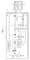
- UPS 10 serving as an "uninterruptible power supply" according to the present invention will be described while referring to FIG. 1 .
- FIG. 1 is a block diagram of the UPS 10.
- An ATX (Advanced Technology extended) power supply 20 serving as an "external power supply” is an apparatus which operates on electrical power supplied from a commercial power source and supplies DC power having a predetermined voltage to a server 30.
- the commonly-used ATX power supply 20 is provided with a general-purpose power failure detection circuit as a standard feature to output a power failure detection signal (PWOK, SMBALERT or the like) when the circuit detects a power failure in the commercial power source.
- the UPS 10 is an apparatus which supplies DC power having a predetermined voltage to the server 30 at the time of an instantaneous power failure in the commercial power source (not illustrated).
- the server 30 is connected to an output terminal 17 of the UPS 10 and an output terminal 21 of the ATX power supply 20.
- the UPS 10 is provided with a battery 11, a step-up chopper circuit 12, a voltage control circuit 13, and a charging circuit 14.
- the battery 11 is, for example, a rechargeable/dischargeable secondary battery, such as a nickel-hydrogen secondary battery.
- the positive electrode of the battery 11 is connected to one end of a switch SW1 and the negative electrode of the battery 11 is connected to the ground.
- the other end of the switch SW1 is connected to the anode terminal of a diode D1. By closing this switch SW1, the electrical power of the battery 11 is supplied to the step-up chopper circuit 12.
- the claimed invention can also be carried out by changing the battery 11 with, for example, a primary battery, without including the charging circuit 14 to be described later.
- the step-up chopper circuit 12 serving as a "power inverter circuit” is a publicly-known step-up circuit used to raise and invert the voltage of the battery 11 to a certain voltage.
- the "power inverter circuit” may alternatively be, for example, a publicly-known step-down chopper circuit or step-up/down chopper circuit.
- the power inverter circuit may be, for example, a publicly-known inverter circuit for inverting the DC power of the battery 11 to AC power according to the specifications of the server 30 or the like.
- the step-up chopper circuit 12 includes a coil L1, a switch SW2, a diode D3, and a switching controller 15.
- the cathode terminal of the diode D3 is connected to the anode terminal of a diode D4, and the cathode terminal of the diode D4 is connected to the output terminal 17.
- the other end of the switch SW2 is connected to the ground.
- the switch SW2 is, for example, a semiconductor switching element, such as a transistor or an FET (field effect transistor).
- the switching controller 15 serving as a "voltage regulator” undertakes the on/off-control of the switch SW2 to adjust the duty ratio thereof, thereby performing control for maintaining the output voltage of the step-up chopper circuit 12 at a constant level. More specifically, the switching controller 15 performs the on/off-control of the switch SW2 to adjust the output voltage, so that a reference voltage V1 to be described later equals a predetermined voltage.
- the voltage control circuit 13 includes a first resistor R1, a second resistor R2, a third resistor R3, a switch SW3 and a voltage controller 16.
- the first resistor R1 and the second resistor R2 constitute a voltage-dividing circuit for dividing the output voltage of the step-up chopper circuit 12.
- the third resistor R3 is connected in parallel with the second resistor R2.
- the switch SW3 is, for example, a semiconductor switching element, such as a transistor or an FET, used to cut off the parallel connection of the third resistor R3 with the second resistor R2.
- the voltage controller 16 is, for example, a publicly-known microcomputer control device used to perform the open/close-control of the switch SW3 on the basis of a power failure detection signal PWOK output by the ATX power supply 20.
- one end of the first resistor R1 is connected to the cathode terminal of the diode D3 and the other end of the first resistor R1 is connected to one end of the resistor R2.
- the other end of the second resistor R2 is connected to the ground.
- One end of the third resistor R3 is connected to the connection point between the first resistor R1 and the second resistor R2, and the other end of the third resistor R3 is connected to one end of the switch SW3.
- the other end of the switch SW3 is connected to the ground.
- the connection point between the first resistor R1 and the second resistor R2 is connected to the switching controller 15 of the step-up chopper circuit 12.
- the voltage of this connection point serves as the reference voltage V1 of the step-up chopper circuit 12.
- the charging circuit 14 is used to charge the battery 11 with the electrical power of the ATX power supply 20. More specifically, the charging circuit 14 is connected to the output terminal 17, and part of electrical power output by the ATX power supply 20 is supplied to the charging circuit 14 through the output terminal 17. In addition, the charging circuit 14 is connected to one end of the switch SW4, and the other end of the switch SW4 is connected to the positive electrode of the battery 11.
- the switch SW4 is, for example, a semiconductor switching element, such as a transistor or an FET.
- the battery 11 is charged by closing this switch SW4.
- the charging circuit 14 open/close-controls the switch SW4 on the basis of the charged state of the battery 11.
- the charging circuit 14 is further connected to the anode terminal of the diode D2, and the cathode terminal of the diode D2 is connected to the cathode terminal of the diode D1.
- the UPS 10 is preferably provided with the charging circuit 14 for charging the battery 11 with the electrical power of the ATX power supply 20. Consequently, the battery 11 can be maintained in a charged state ready to supply an adequate amount of electrical power at the time of an instantaneous power failure. It is therefore possible to prevent such a situation that the UPS 10 fails to supply an adequate amount of electrical power from the battery 11 at the time of an instantaneous power failure, and therefore, the voltage of electrical power supplied to the server 30 drops temporarily.
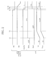
- the operation of the UPS 10 will be described while referring to FIG. 2 .
- FIG. 2 is a timing chart illustrating the operation of the UPS 10 and the ATX power supply 20.
- the UPS 10 is operative so that the step-up chopper circuit 12 starts voltage boosting as the result of the switch SW1 being placed in a closed state (ON) (timing T1). Consequently, the reference voltage V1 rises to a predetermined voltage, and the output voltage Vout (voltage of the output terminal 17) of the step-up chopper circuit 12 rises from 0 V to a standby voltage Vout1 (timing T2).
- the standby voltage Vout1 is lower than a rated voltage Vout2.
- the rated voltage Vout2 is 12 V
- the standby voltage Vout1 is set to a voltage of approximately 10.9 V which is nearly 90% of the rated voltage.
- the output voltage Vout of the step-up chopper circuit 12 is maintained at the standby voltage Vout1.
- the power failure detection signal PWOK of the ATX power supply 20 changes from a high (H) level to a low (L) level in approximately 12 ms at the minimum from the time supply of electrical power to the ATX power supply 20 stops (timing T4).
- the direct-current voltage output DC of the ATX power supply 20 begins to drop in approximately 13 ms at the minimum from the time supply of electrical power to the ATX power supply 20 stops (timing T6). That is, in the ATX power supply 20, the time difference from the time the power failure detection signal PWOK changes to a low (L) level to the time the voltage of the direct-current voltage output DC begins to drop is only approximately 1 ms.
- the UPS 10 places the SW3 in a closed state (ON) at the timing when the power failure detection signal PWOK changes from a high (H) level to a low (L) level (timing T4).
- the third resistor R3 is connected in parallel with the second resistor R2. Consequently, a voltage dividing ratio changes and the reference voltage V1 becomes lower than the predetermined voltage (timing T4).
- the switching controller 15 of the step-up chopper circuit 12 adjusts the duty ratio of a control signal applied to the switch SW2, so that the reference voltage V1 equals the predetermined voltage. Consequently, the output voltage Vout of the step-up chopper circuit 12 rises from the standby voltage Vout1 to the rated voltage Vout2 (timing T5). That is, under the condition of the power failure detection signal PWOK being output from the ATX power supply 20 (the power failure detection signal PWOK is in a low (L) level), the output voltage Vout of the step-up chopper circuit 12 equals the rated voltage Vout2.
- Timing T4 This time period from the time the switch SW3 is closed (timing T4) to the time the output voltage Vout of the step-up chopper circuit 12 rises to the rated voltage Vout2 (timing T5) is approximately 0.5 ms.
- This time lag is shorter than the time difference of 1 ms from the time the power failure detection signal PWOK changes to a low (L) level to the time the voltage of the direct-current voltage output DC begins to drop.
- the UPS 10 can set the output voltage of the step-up chopper circuit 12 to the rated voltage Vout2 (12 V DC) before the voltage of the direct-current voltage output DC of the ATX power supply 20 begins to drop. Accordingly, there hardly arises the possibility that in the UPS 10, the voltage of electrical power supplied to the server 30 drops temporarily at the time of an instantaneous power failure in the commercial power source.
- the UPS 10 maintains the output voltage Vout of the step-up chopper circuit 12 at the standby voltage Vout1 lower than the rated voltage under the condition of the power failure detection signal PWOK being not output from the ATX power supply 20.
- the UPS 10 controls the step-up chopper circuit 12, so that the output voltage Vout thereof equals the rated voltage Vout2. Consequently, it is possible to greatly reduce the time difference from the time the power failure detection signal PWOK is detected to the time the UPS 10 is ready to supply electrical power having the rated voltage Vout2.
- the UPS 10 maintains the output voltage Vout of the step-up chopper circuit 12 at the standby voltage Vout1 lower than the rated voltage Vout2 during standby. For this reason, the electrical power of the battery 11 of the UPS 10 is hardly consumed at all during the time electrical power is supplied from the ATX power supply 20 to the server 30. Accordingly, there arises no such a situation that the electrical power of the battery 11 is consumed during standby, thus failing to meet the essential requirement of supplying electrical power from the UPS 10 to the server 30 at the time of an instantaneous power failure.
- the UPS 10 it is possible to provide the UPS 10, at low cost, in which the voltage of electrical power supplied to electronic equipment, such as the server 30, is less likely to drop temporarily at the time of an instantaneous power failure in the commercial power source.
- the voltage control circuit 13 is configured so that the output voltage Vout of the step-up chopper circuit 12 can be raised from the standby voltage Vout1 to the rated voltage Vout2 simply by closing the switch SW3 to connect the third resistor R3 in parallel with the second resistor R2. Consequently, the output voltage Vout of the step-up chopper circuit 12 can be raised to the rated voltage Vout2 in a shorter period of time from the point in time when the power failure detection signal PWOK is output from the ATX power supply 20. Thus, it is possible to further reduce the possibility of the voltage of electrical power supplied to the server 30 dropping temporarily at the time of an instantaneous power failure in the commercial power source.
Landscapes
- Engineering & Computer Science (AREA)
- Power Engineering (AREA)
- Business, Economics & Management (AREA)
- Emergency Management (AREA)
- Stand-By Power Supply Arrangements (AREA)
- Measurement Of Current Or Voltage (AREA)
- Dc-Dc Converters (AREA)
- Charge And Discharge Circuits For Batteries Or The Like (AREA)
Abstract
Description
- The present invention relates to an uninterruptible power supply.
- In an external power supply for converting the electricity of a commercial power source to electrical power having a predetermined voltage to supply the power to electronic equipment, the voltage of the electrical power supplied to the electronic equipment temporarily drops if an instantaneous power failure occurs in the commercial power source, thus possibly causing problems with the operation of the electronic equipment. For this reason, there has been a publicly-known uninterruptible power supply used to detect the instantaneous power failure in the commercial power source by a power failure detection signal output by the external power supply and supply electrical power from a backup battery or the like to the electronic equipment in case of an instantaneous power failure.
- In general, a comparatively long time lag from the time an instantaneous power failure occurs to the time the external power supply outputs a power failure detection signal is in many cases associated with a general-purpose power failure detection circuit included in the external power supply as a standard feature. In addition, a conventional uninterruptible power supply starts up a converter circuit, an inverter circuit, and the like included therein only after detecting the power failure detection signal. This means that a certain period of time is required until the uninterruptible power supply is ready to supply electrical power having a rated voltage, from the time the power failure detection signal is detected. Accordingly, the uninterruptible power supply may fail to back up in time if electrical power supply from the commercial power source to the external power supply stops due to the instantaneous power failure, though there is more or less the time difference from when the instantaneous power failure occurs to when the output voltage of the external power supply drops. Consequently, the voltage of electrical power supplied to the electronic equipment may drop temporarily.
- As a related art intended to solve such problems as described above, there has been publicly known a power failure detector or the like for rapidly detecting an instantaneous power failure in a commercial power source (see Japanese Patent Laid-Open Nos.
10-19943 2001-13175 2006-126135 2007-225427 - The power failure detector for rapidly detecting the instantaneous power failure in the commercial power source is generally complex in configuration and large in scale and requires great amounts of cost and time for development, however. The power failure detector is thus extremely expensive in many cases.
- An object of the present invention, which has been accomplished in view of such circumstances as described above, is to provide an uninterruptible power supply, at low cost, in which the voltage of electrical power supplied to electronic equipment is less likely to drop temporarily even if an instantaneous power failure occurs in a commercial power source.
- A first aspect of the present invention is an uninterruptible power supply provided with a battery, a power inverter circuit for inverting the electrical power of the battery, and a voltage control circuit for controlling the power inverter circuit, so that the output voltage of the power inverter circuit is maintained at a standby voltage lower than a rated voltage under the condition of a power failure detection signal being not output from an external power supply and the output voltage of the power inverter circuit equals the rated voltage under the condition of the power failure detection signal being output from the external power supply.
- As described above, the power inverter circuit is controlled so that the output voltage of the power inverter circuit is maintained at the standby voltage lower than the rated voltage under the condition of a power failure detection signal being not output from the external power supply and the output voltage of the power inverter circuit equals the rated voltage when a power failure detection signal is output from the external power supply. Consequently, it is possible to greatly reduce the time difference from the time the power failure detection signal is detected to the time the uninterruptible power supply is ready to supply electrical power having the rated voltage. Accordingly, the possibility of the voltage of electrical power supplied to the electronic equipment dropping temporarily when an instantaneous power failure occurs in the commercial power source can be reduced without having to provide any expensive power failure detector.
- In addition, the uninterruptible power supply maintains the output voltage of the power inverter circuit at the standby voltage lower than the rated voltage during standby. For this reason, the electrical power of the battery of the uninterruptible power supply is hardly consumed at all during the time electrical power is supplied from the external power supply to the electronic equipment at the rated voltage. Accordingly, there arises no such a situation that the electrical power of the battery is consumed during standby, thus failing to meet the essential requirement of supplying electrical power from the uninterruptible power supply at the time of an instantaneous power failure.
- Thus, according to the first aspect of the present invention, there is obtained a working effect of being able to provide an uninterruptible power supply, at low cost, in which the voltage of electrical power supplied to the electronic equipment is less likely to drop temporarily at the time of an instantaneous power failure in the commercial power source.
- A second aspect of the present invention is an uninterruptible power supply characterized in that in the above-described first aspect of the present invention, the voltage control circuit includes: a first resistor and a second resistor for dividing the output voltage of the power inverter circuit; a third resistor connected in parallel with the second resistor; a switch for cutting off the parallel connection of the third resistor with the second resistor; and a voltage controller for controlling the switch on the basis of the power failure detection signal, and the power inverter circuit includes a voltage regulator for regulating the output voltage, so that the voltage of the connection point between the first resistor and the second resistor equals a predetermined voltage.
- According to such a characteristic as described above, the output voltage of the power inverter circuit can be controlled simply by changing a voltage dividing ratio by the open/close-control of the switch. More specifically, the output voltage of the power inverter circuit can be raised from the standby voltage to the rated voltage simply by changing the voltage dividing ratio by closing the switch to connect the third resistor in parallel with the second resistor when a power failure detection signal is output from the external power supply. Consequently, the output voltage of the power inverter circuit can be raised to the rated voltage in a shorter period of time from the point in time when the power failure detection signal is output from the external power supply. Thus, it is possible to further reduce the possibility of the voltage of electrical power supplied to the electronic equipment dropping temporarily at the time of an instantaneous power failure in a commercial power source.
- A third aspect of the present invention is an uninterruptible power supply characterized in that in the above-described first or second aspect of the present invention, the uninterruptible power supply further includes a charging circuit for charging the battery with the electrical power of the external power supply.
- According to such a characteristic as described above, the battery can be maintained in a charged state ready to supply an adequate amount of electrical power at the time of an instantaneous power failure. It is therefore possible to prevent such a situation that the uninterruptible power supply fails to supply an adequate amount of electrical power from the battery at the time of an instantaneous power failure, and therefore, the voltage of electrical power supplied to the electronic equipment drops temporarily.
-
-
FIG. 1 is a block diagram of a UPS; and -
FIG. 2 is a timing chart illustrating the operation of an UPS and an ATX power supply. - Hereinafter, embodiments of the present invention will be described while referring to the accompanying drawings.
- The configuration of a UPS 10 serving as an "uninterruptible power supply" according to the present invention will be described while referring to
FIG. 1 . -
FIG. 1 is a block diagram of the UPS 10. - An ATX (Advanced Technology extended)
power supply 20 serving as an "external power supply" is an apparatus which operates on electrical power supplied from a commercial power source and supplies DC power having a predetermined voltage to aserver 30. The commonly-used ATXpower supply 20 is provided with a general-purpose power failure detection circuit as a standard feature to output a power failure detection signal (PWOK, SMBALERT or the like) when the circuit detects a power failure in the commercial power source. The UPS 10 is an apparatus which supplies DC power having a predetermined voltage to theserver 30 at the time of an instantaneous power failure in the commercial power source (not illustrated). Theserver 30 is connected to anoutput terminal 17 of the UPS 10 and anoutput terminal 21 of the ATXpower supply 20. - The UPS 10 is provided with a
battery 11, a step-up chopper circuit 12, avoltage control circuit 13, and acharging circuit 14. - The
battery 11 is, for example, a rechargeable/dischargeable secondary battery, such as a nickel-hydrogen secondary battery. The positive electrode of thebattery 11 is connected to one end of a switch SW1 and the negative electrode of thebattery 11 is connected to the ground. The other end of the switch SW1 is connected to the anode terminal of a diode D1. By closing this switch SW1, the electrical power of thebattery 11 is supplied to the step-up chopper circuit 12. - Note that the claimed invention can also be carried out by changing the
battery 11 with, for example, a primary battery, without including thecharging circuit 14 to be described later. - The step-
up chopper circuit 12 serving as a "power inverter circuit" is a publicly-known step-up circuit used to raise and invert the voltage of thebattery 11 to a certain voltage. The "power inverter circuit" may alternatively be, for example, a publicly-known step-down chopper circuit or step-up/down chopper circuit. Yet alternatively, the power inverter circuit may be, for example, a publicly-known inverter circuit for inverting the DC power of thebattery 11 to AC power according to the specifications of theserver 30 or the like. - The step-
up chopper circuit 12 includes a coil L1, a switch SW2, a diode D3, and aswitching controller 15. - One end of the coil L1 is connected to the cathode terminal of the diode D1 and the other end of the coil L1 is connected to the anode terminal of the diode D3 and one end of the switch SW2. The cathode terminal of the diode D3 is connected to the anode terminal of a diode D4, and the cathode terminal of the diode D4 is connected to the
output terminal 17. The other end of the switch SW2 is connected to the ground. The switch SW2 is, for example, a semiconductor switching element, such as a transistor or an FET (field effect transistor). Theswitching controller 15 serving as a "voltage regulator" undertakes the on/off-control of the switch SW2 to adjust the duty ratio thereof, thereby performing control for maintaining the output voltage of the step-up chopper circuit 12 at a constant level. More specifically, theswitching controller 15 performs the on/off-control of the switch SW2 to adjust the output voltage, so that a reference voltage V1 to be described later equals a predetermined voltage. - The
voltage control circuit 13 includes a first resistor R1, a second resistor R2, a third resistor R3, a switch SW3 and avoltage controller 16. - The first resistor R1 and the second resistor R2 constitute a voltage-dividing circuit for dividing the output voltage of the step-up
chopper circuit 12. The third resistor R3 is connected in parallel with the second resistor R2. The switch SW3 is, for example, a semiconductor switching element, such as a transistor or an FET, used to cut off the parallel connection of the third resistor R3 with the second resistor R2. Thevoltage controller 16 is, for example, a publicly-known microcomputer control device used to perform the open/close-control of the switch SW3 on the basis of a power failure detection signal PWOK output by theATX power supply 20. - More specifically, one end of the first resistor R1 is connected to the cathode terminal of the diode D3 and the other end of the first resistor R1 is connected to one end of the resistor R2. The other end of the second resistor R2 is connected to the ground. One end of the third resistor R3 is connected to the connection point between the first resistor R1 and the second resistor R2, and the other end of the third resistor R3 is connected to one end of the switch SW3. The other end of the switch SW3 is connected to the ground. The connection point between the first resistor R1 and the second resistor R2 is connected to the switching
controller 15 of the step-upchopper circuit 12. The voltage of this connection point serves as the reference voltage V1 of the step-upchopper circuit 12. - The charging
circuit 14 is used to charge thebattery 11 with the electrical power of theATX power supply 20. More specifically, the chargingcircuit 14 is connected to theoutput terminal 17, and part of electrical power output by theATX power supply 20 is supplied to the chargingcircuit 14 through theoutput terminal 17. In addition, the chargingcircuit 14 is connected to one end of the switch SW4, and the other end of the switch SW4 is connected to the positive electrode of thebattery 11. The switch SW4 is, for example, a semiconductor switching element, such as a transistor or an FET. Thebattery 11 is charged by closing this switch SW4. The chargingcircuit 14 open/close-controls the switch SW4 on the basis of the charged state of thebattery 11. The chargingcircuit 14 is further connected to the anode terminal of the diode D2, and the cathode terminal of the diode D2 is connected to the cathode terminal of the diode D1. - As described above, the
UPS 10 is preferably provided with the chargingcircuit 14 for charging thebattery 11 with the electrical power of theATX power supply 20. Consequently, thebattery 11 can be maintained in a charged state ready to supply an adequate amount of electrical power at the time of an instantaneous power failure. It is therefore possible to prevent such a situation that theUPS 10 fails to supply an adequate amount of electrical power from thebattery 11 at the time of an instantaneous power failure, and therefore, the voltage of electrical power supplied to theserver 30 drops temporarily. - The operation of the
UPS 10 will be described while referring toFIG. 2 . -
FIG. 2 is a timing chart illustrating the operation of theUPS 10 and theATX power supply 20. - The
UPS 10 is operative so that the step-upchopper circuit 12 starts voltage boosting as the result of the switch SW1 being placed in a closed state (ON) (timing T1). Consequently, the reference voltage V1 rises to a predetermined voltage, and the output voltage Vout (voltage of the output terminal 17) of the step-upchopper circuit 12 rises from 0 V to a standby voltage Vout1 (timing T2). The standby voltage Vout1 is lower than a rated voltage Vout2. For example, in the present embodiment, the rated voltage Vout2 is 12 V, whereas the standby voltage Vout1 is set to a voltage of approximately 10.9 V which is nearly 90% of the rated voltage. Under the condition of the power failure detection signal PWOK being not output from the ATX power supply 20 (the power failure detection signal PWOK is in a high (H) level), the output voltage Vout of the step-upchopper circuit 12 is maintained at the standby voltage Vout1. - Note that a time period of approximately 5 ms is taken for the output voltage Vout of the step-up
chopper circuit 12 to rise from 0 V to the standby voltage Vout1 (timing T2) from the time the switch SW1 is closed (timing T1). - If an instantaneous power failure occurs in the commercial power source and supply of alternating-current power AC to the
ATX power supply 20 stops (timing T3), the power failure detection signal PWOK of theATX power supply 20 changes from a high (H) level to a low (L) level in approximately 12 ms at the minimum from the time supply of electrical power to theATX power supply 20 stops (timing T4). Then, the direct-current voltage output DC of theATX power supply 20 begins to drop in approximately 13 ms at the minimum from the time supply of electrical power to theATX power supply 20 stops (timing T6). That is, in theATX power supply 20, the time difference from the time the power failure detection signal PWOK changes to a low (L) level to the time the voltage of the direct-current voltage output DC begins to drop is only approximately 1 ms. - The
UPS 10 places the SW3 in a closed state (ON) at the timing when the power failure detection signal PWOK changes from a high (H) level to a low (L) level (timing T4). At the moment the SW3 is closed, the third resistor R3 is connected in parallel with the second resistor R2. Consequently, a voltage dividing ratio changes and the reference voltage V1 becomes lower than the predetermined voltage (timing T4). - When the reference voltage V1 becomes lower than the predetermined voltage, the switching
controller 15 of the step-upchopper circuit 12 adjusts the duty ratio of a control signal applied to the switch SW2, so that the reference voltage V1 equals the predetermined voltage. Consequently, the output voltage Vout of the step-upchopper circuit 12 rises from the standby voltage Vout1 to the rated voltage Vout2 (timing T5). That is, under the condition of the power failure detection signal PWOK being output from the ATX power supply 20 (the power failure detection signal PWOK is in a low (L) level), the output voltage Vout of the step-upchopper circuit 12 equals the rated voltage Vout2. - This time period from the time the switch SW3 is closed (timing T4) to the time the output voltage Vout of the step-up
chopper circuit 12 rises to the rated voltage Vout2 (timing T5) is approximately 0.5 ms. This time lag is shorter than the time difference of 1 ms from the time the power failure detection signal PWOK changes to a low (L) level to the time the voltage of the direct-current voltage output DC begins to drop. This means that if an instantaneous power failure occurs and the power failure detection signal PWOK of theATX power supply 20 changes to a low (L) level, theUPS 10 can set the output voltage of the step-upchopper circuit 12 to the rated voltage Vout2 (12 V DC) before the voltage of the direct-current voltage output DC of theATX power supply 20 begins to drop. Accordingly, there hardly arises the possibility that in theUPS 10, the voltage of electrical power supplied to theserver 30 drops temporarily at the time of an instantaneous power failure in the commercial power source. - As described above, the
UPS 10 according to the present invention maintains the output voltage Vout of the step-upchopper circuit 12 at the standby voltage Vout1 lower than the rated voltage under the condition of the power failure detection signal PWOK being not output from theATX power supply 20. When the power failure detection signal PWOK is output from theATX power supply 20, theUPS 10 controls the step-upchopper circuit 12, so that the output voltage Vout thereof equals the rated voltage Vout2. Consequently, it is possible to greatly reduce the time difference from the time the power failure detection signal PWOK is detected to the time theUPS 10 is ready to supply electrical power having the rated voltage Vout2. Accordingly, it is possible to reduce the possibility of the voltage of electrical power supplied to theserver 30 dropping temporarily at the time of an instantaneous power failure in the commercial power source and realize seamless backup by thevoltage control circuit 13 having an extremely simple configuration, without having to provide any expensive power failure detector. - In addition, the
UPS 10 maintains the output voltage Vout of the step-upchopper circuit 12 at the standby voltage Vout1 lower than the rated voltage Vout2 during standby. For this reason, the electrical power of thebattery 11 of theUPS 10 is hardly consumed at all during the time electrical power is supplied from theATX power supply 20 to theserver 30. Accordingly, there arises no such a situation that the electrical power of thebattery 11 is consumed during standby, thus failing to meet the essential requirement of supplying electrical power from theUPS 10 to theserver 30 at the time of an instantaneous power failure. - Thus, according to the present invention, it is possible to provide the
UPS 10, at low cost, in which the voltage of electrical power supplied to electronic equipment, such as theserver 30, is less likely to drop temporarily at the time of an instantaneous power failure in the commercial power source. - In addition, the
voltage control circuit 13 is configured so that the output voltage Vout of the step-upchopper circuit 12 can be raised from the standby voltage Vout1 to the rated voltage Vout2 simply by closing the switch SW3 to connect the third resistor R3 in parallel with the second resistor R2. Consequently, the output voltage Vout of the step-upchopper circuit 12 can be raised to the rated voltage Vout2 in a shorter period of time from the point in time when the power failure detection signal PWOK is output from theATX power supply 20. Thus, it is possible to further reduce the possibility of the voltage of electrical power supplied to theserver 30 dropping temporarily at the time of an instantaneous power failure in the commercial power source. - It should be noted that needless to say, the present invention is not limited to the above-described embodiments but may be modified in various other ways within the scope of the present invention as defined by the claims appended hereto.
Claims (3)
- An uninterruptible power supply (10) provided with a battery (11) and a power inverter circuit (12) for inverting the electrical power of the battery (11), characterized in that
the uninterruptible power supply (10) includes a voltage control circuit (13) for controlling the power inverter circuit (12), so that the output voltage of the power inverter circuit (12) is maintained at a standby voltage lower than a rated voltage under the condition of a power failure detection signal being not output from an external power supply and the output voltage of the power inverter circuit (12) equals the rated voltage under the condition of the power failure detection signal being output from the external power supply. - The uninterruptible power supply (10) according to claim 1, characterized in that
the voltage control circuit (13) includes a first resistor (R1) and a second resistor (R2) for dividing the output voltage of the power inverter circuit (12); a third resistor (R3) connected in parallel with the second resistor (R2); a switch (SW3) for cutting off the parallel connection of the third resistor (R3) with the second resistor (R2); and a voltage controller (16) for controlling the switch (SW3) on the basis of the power failure detection signal, and
the power inverter circuit (12) includes a voltage regulator (15) for regulating the output voltage, so that the voltage of the connection point between the first resistor (R1) and the second resistor (R2) equals a predetermined voltage. - The uninterruptible power supply (10) according to claim 1 or 2, characterized in that the uninterruptible power supply (10) further includes a charging circuit (14) for charging the battery (11) with the electrical power of the external power supply.
Applications Claiming Priority (1)
| Application Number | Priority Date | Filing Date | Title |
|---|---|---|---|
| JP2012284074A JP2014128142A (en) | 2012-12-27 | 2012-12-27 | Uninterruptible power supply unit |
Publications (2)
| Publication Number | Publication Date |
|---|---|
| EP2750262A1 true EP2750262A1 (en) | 2014-07-02 |
| EP2750262B1 EP2750262B1 (en) | 2018-04-11 |
Family
ID=49876368
Family Applications (1)
| Application Number | Title | Priority Date | Filing Date |
|---|---|---|---|
| EP13196926.3A Not-in-force EP2750262B1 (en) | 2012-12-27 | 2013-12-12 | Uninterruptible power supply |
Country Status (4)
| Country | Link |
|---|---|
| US (1) | US9490661B2 (en) |
| EP (1) | EP2750262B1 (en) |
| JP (1) | JP2014128142A (en) |
| CN (1) | CN103904771B (en) |
Cited By (4)
| Publication number | Priority date | Publication date | Assignee | Title |
|---|---|---|---|---|
| WO2016085844A1 (en) * | 2014-11-24 | 2016-06-02 | Technicolor Usa, Inc. | Battery backup arrangement |
| RU191699U1 (en) * | 2019-02-04 | 2019-08-16 | федеральное государственное бюджетное образовательное учреждение высшего образования "Ставропольский государственный аграрный университет" | Backup Power Device |
| EP3893360A1 (en) * | 2020-04-08 | 2021-10-13 | Rohde & Schwarz GmbH & Co. KG | Power supply, communication device and method for controlling a power supply |
| US11571534B2 (en) * | 2016-05-11 | 2023-02-07 | ResMed Pty Ltd | Power supply for respiratory therapy device |
Families Citing this family (7)
| Publication number | Priority date | Publication date | Assignee | Title |
|---|---|---|---|---|
| US9552031B2 (en) * | 2013-12-20 | 2017-01-24 | Facebook, Inc. | Power shelf for computer servers |
| CN104333113B (en) * | 2014-10-31 | 2017-12-05 | 许继电气股份有限公司 | A kind of power circuit |
| CN106119080A (en) * | 2016-07-06 | 2016-11-16 | 车团结 | A kind of instrument for extracting nucleic acid and power-supply system thereof |
| US10505390B2 (en) * | 2018-03-05 | 2019-12-10 | Ig Soo Kwon | Power blackout sensing system with a phantom voltage detector including a coupled inductor device |
| US10620692B2 (en) * | 2018-08-01 | 2020-04-14 | Dell Products L.P. | System and method of operating one or more information handling systems |
| JP7255249B2 (en) * | 2019-03-12 | 2023-04-11 | 富士通株式会社 | Power supply circuit and electronic device |
| JP2022020442A (en) * | 2020-07-20 | 2022-02-01 | Fdk株式会社 | Control device, battery pack, and power supply device |
Citations (8)
| Publication number | Priority date | Publication date | Assignee | Title |
|---|---|---|---|---|
| US4401895A (en) * | 1982-09-20 | 1983-08-30 | Reliance Electric Company | Supply for providing uninterruptible d-c power to a load |
| JPH1019943A (en) | 1996-07-04 | 1998-01-23 | Fuji Electric Co Ltd | Detecting circuit of interruption of power supply in uninterruptible power supply unit |
| US5894413A (en) * | 1997-01-28 | 1999-04-13 | Sony Corporation | Redundant power supply switchover circuit |
| JP2001013175A (en) | 1999-06-25 | 2001-01-19 | Shin Kobe Electric Mach Co Ltd | Service interruption detecting method and uninterruptible power source device using it |
| US20050121979A1 (en) * | 2003-12-09 | 2005-06-09 | Matsushita Electric Industrial Co., Ltd. | Direct-current uninterruptible power source unit |
| CN2715411Y (en) * | 2004-07-07 | 2005-08-03 | 杭州中信网络自动化有限公司 | Dedicated DC UPS for switch power supply input load |
| JP2006126135A (en) | 2004-11-01 | 2006-05-18 | Densei Lambda Kk | Power failure sensitive device, power source switching unit, uninterruptible power system, and program for power failure sensing |
| JP2007225427A (en) | 2006-02-23 | 2007-09-06 | Fuji Electric Systems Co Ltd | Power interruption detecting circuit and uninterruptible power supply unit |
Family Cites Families (7)
| Publication number | Priority date | Publication date | Assignee | Title |
|---|---|---|---|---|
| JPS61116969A (en) * | 1984-11-13 | 1986-06-04 | Nec Corp | Parallel operation switching power source |
| DE4323940C2 (en) * | 1993-07-16 | 1996-07-11 | Siemens Nixdorf Inf Syst | DC voltage supply system with at least one clocked DC voltage power supply |
| JP5170610B2 (en) * | 2006-02-28 | 2013-03-27 | 日立工機株式会社 | Charger |
| JP2009148110A (en) * | 2007-12-17 | 2009-07-02 | Nippon Telegr & Teleph Corp <Ntt> | Charger/discharger and power supply device using the same |
| JP2010068639A (en) * | 2008-09-11 | 2010-03-25 | Seiko Epson Corp | Battery unit and power supply device |
| JP5129788B2 (en) * | 2009-07-13 | 2013-01-30 | 富士通株式会社 | Power supply device and power supply control method |
| CN102751872B (en) * | 2011-04-21 | 2016-04-06 | 登丰微电子股份有限公司 | Feedback control circuit |
-
2012
- 2012-12-27 JP JP2012284074A patent/JP2014128142A/en active Pending
-
2013
- 2013-12-12 EP EP13196926.3A patent/EP2750262B1/en not_active Not-in-force
- 2013-12-20 US US14/137,836 patent/US9490661B2/en active Active
- 2013-12-26 CN CN201310733002.7A patent/CN103904771B/en not_active Expired - Fee Related
Patent Citations (8)
| Publication number | Priority date | Publication date | Assignee | Title |
|---|---|---|---|---|
| US4401895A (en) * | 1982-09-20 | 1983-08-30 | Reliance Electric Company | Supply for providing uninterruptible d-c power to a load |
| JPH1019943A (en) | 1996-07-04 | 1998-01-23 | Fuji Electric Co Ltd | Detecting circuit of interruption of power supply in uninterruptible power supply unit |
| US5894413A (en) * | 1997-01-28 | 1999-04-13 | Sony Corporation | Redundant power supply switchover circuit |
| JP2001013175A (en) | 1999-06-25 | 2001-01-19 | Shin Kobe Electric Mach Co Ltd | Service interruption detecting method and uninterruptible power source device using it |
| US20050121979A1 (en) * | 2003-12-09 | 2005-06-09 | Matsushita Electric Industrial Co., Ltd. | Direct-current uninterruptible power source unit |
| CN2715411Y (en) * | 2004-07-07 | 2005-08-03 | 杭州中信网络自动化有限公司 | Dedicated DC UPS for switch power supply input load |
| JP2006126135A (en) | 2004-11-01 | 2006-05-18 | Densei Lambda Kk | Power failure sensitive device, power source switching unit, uninterruptible power system, and program for power failure sensing |
| JP2007225427A (en) | 2006-02-23 | 2007-09-06 | Fuji Electric Systems Co Ltd | Power interruption detecting circuit and uninterruptible power supply unit |
Non-Patent Citations (1)
| Title |
|---|
| "2.25 MHz 400-mA Step Down Converter With Selectable VOUT", 1 January 2009 (2009-01-01), pages 1 - 25, XP055103159, Retrieved from the Internet <URL:http://www.ti.com/lit/ds/symlink/tps62272.pdf> [retrieved on 20140219] * |
Cited By (4)
| Publication number | Priority date | Publication date | Assignee | Title |
|---|---|---|---|---|
| WO2016085844A1 (en) * | 2014-11-24 | 2016-06-02 | Technicolor Usa, Inc. | Battery backup arrangement |
| US11571534B2 (en) * | 2016-05-11 | 2023-02-07 | ResMed Pty Ltd | Power supply for respiratory therapy device |
| RU191699U1 (en) * | 2019-02-04 | 2019-08-16 | федеральное государственное бюджетное образовательное учреждение высшего образования "Ставропольский государственный аграрный университет" | Backup Power Device |
| EP3893360A1 (en) * | 2020-04-08 | 2021-10-13 | Rohde & Schwarz GmbH & Co. KG | Power supply, communication device and method for controlling a power supply |
Also Published As
| Publication number | Publication date |
|---|---|
| EP2750262B1 (en) | 2018-04-11 |
| CN103904771B (en) | 2017-11-24 |
| US9490661B2 (en) | 2016-11-08 |
| CN103904771A (en) | 2014-07-02 |
| JP2014128142A (en) | 2014-07-07 |
| US20140183959A1 (en) | 2014-07-03 |
Similar Documents
| Publication | Publication Date | Title |
|---|---|---|
| US9490661B2 (en) | Uninterruptible power supply | |
| US7948212B2 (en) | Battery pack and charging method | |
| US6225708B1 (en) | Uninterruptable power supply | |
| JP3747381B2 (en) | Power supply control circuit for electronic devices with built-in batteries | |
| US9825478B2 (en) | Method for supplying power to a load within a portable electronic device | |
| US9502917B2 (en) | Charging method of electronic cigarettes and electronic cigarette box | |
| EP2515422B1 (en) | Analog current limit adjustment for linear and switching regulators | |
| US7932636B2 (en) | Automatic start-up circuit and uninterruptible power supply apparatus having such automatic start-up circuit | |
| US11290801B2 (en) | Headset charging system and headset charging method | |
| US9917466B2 (en) | DC power source and associated methods of operating same to efficiently supply a specification-compliant output voltage | |
| KR20130009599A (en) | Battery charging apparatus with a common control loop for a low drop-out voltage regulator and a boost regulator | |
| JP2013042627A (en) | Dc power supply control device and dc power supply control method | |
| US20150084581A1 (en) | Charging device configured to reduce power consumption during non-charging period | |
| EP3168961B1 (en) | Uninterruptible power source device | |
| JP4946226B2 (en) | DC-DC converter and power supply device | |
| EP4297232A1 (en) | Energy system, and charging and discharging control method | |
| EP3591801A1 (en) | Adaptive charger | |
| CN113572355B (en) | Power supply circuit with stable output voltage | |
| US9035622B2 (en) | Charging device with battery management system for rechargeable battery | |
| KR101663445B1 (en) | The uninterruptible power supply system using energy storage system, and operating method of the uninterruptible power supply system | |
| CN110838747B (en) | Power supply control method of mobile power supply and mobile power supply | |
| JP2015213384A (en) | Battery voltage compensation system | |
| US20120086393A1 (en) | Device and Method for an Intermittent Load | |
| JP2008035573A (en) | Electricity accumulation device employing electric double layer capacitor | |
| WO2019058821A1 (en) | Power storage apparatus |
Legal Events
| Date | Code | Title | Description |
|---|---|---|---|
| 17P | Request for examination filed |
Effective date: 20131212 |
|
| AK | Designated contracting states |
Kind code of ref document: A1 Designated state(s): AL AT BE BG CH CY CZ DE DK EE ES FI FR GB GR HR HU IE IS IT LI LT LU LV MC MK MT NL NO PL PT RO RS SE SI SK SM TR |
|
| AX | Request for extension of the european patent |
Extension state: BA ME |
|
| PUAI | Public reference made under article 153(3) epc to a published international application that has entered the european phase |
Free format text: ORIGINAL CODE: 0009012 |
|
| R17P | Request for examination filed (corrected) |
Effective date: 20141218 |
|
| RBV | Designated contracting states (corrected) |
Designated state(s): AL AT BE BG CH CY CZ DE DK EE ES FI FR GB GR HR HU IE IS IT LI LT LU LV MC MK MT NL NO PL PT RO RS SE SI SK SM TR |
|
| RAP1 | Party data changed (applicant data changed or rights of an application transferred) |
Owner name: FDK CORPORATION |
|
| 17Q | First examination report despatched |
Effective date: 20160226 |
|
| GRAP | Despatch of communication of intention to grant a patent |
Free format text: ORIGINAL CODE: EPIDOSNIGR1 |
|
| RIC1 | Information provided on ipc code assigned before grant |
Ipc: H02M 3/156 20060101ALN20170928BHEP Ipc: H02J 9/06 20060101AFI20170928BHEP |
|
| RIC1 | Information provided on ipc code assigned before grant |
Ipc: H02J 9/06 20060101AFI20171005BHEP Ipc: H02M 3/156 20060101ALN20171005BHEP |
|
| INTG | Intention to grant announced |
Effective date: 20171031 |
|
| GRAS | Grant fee paid |
Free format text: ORIGINAL CODE: EPIDOSNIGR3 |
|
| GRAA | (expected) grant |
Free format text: ORIGINAL CODE: 0009210 |
|
| AK | Designated contracting states |
Kind code of ref document: B1 Designated state(s): AL AT BE BG CH CY CZ DE DK EE ES FI FR GB GR HR HU IE IS IT LI LT LU LV MC MK MT NL NO PL PT RO RS SE SI SK SM TR |
|
| REG | Reference to a national code |
Ref country code: GB Ref legal event code: FG4D |
|
| REG | Reference to a national code |
Ref country code: CH Ref legal event code: EP |
|
| REG | Reference to a national code |
Ref country code: AT Ref legal event code: REF Ref document number: 989015 Country of ref document: AT Kind code of ref document: T Effective date: 20180415 |
|
| REG | Reference to a national code |
Ref country code: IE Ref legal event code: FG4D |
|
| REG | Reference to a national code |
Ref country code: DE Ref legal event code: R096 Ref document number: 602013035660 Country of ref document: DE |
|
| REG | Reference to a national code |
Ref country code: NL Ref legal event code: MP Effective date: 20180411 |
|
| REG | Reference to a national code |
Ref country code: LT Ref legal event code: MG4D |
|
| PG25 | Lapsed in a contracting state [announced via postgrant information from national office to epo] |
Ref country code: NL Free format text: LAPSE BECAUSE OF FAILURE TO SUBMIT A TRANSLATION OF THE DESCRIPTION OR TO PAY THE FEE WITHIN THE PRESCRIBED TIME-LIMIT Effective date: 20180411 |
|
| PG25 | Lapsed in a contracting state [announced via postgrant information from national office to epo] |
Ref country code: BG Free format text: LAPSE BECAUSE OF FAILURE TO SUBMIT A TRANSLATION OF THE DESCRIPTION OR TO PAY THE FEE WITHIN THE PRESCRIBED TIME-LIMIT Effective date: 20180711 Ref country code: FI Free format text: LAPSE BECAUSE OF FAILURE TO SUBMIT A TRANSLATION OF THE DESCRIPTION OR TO PAY THE FEE WITHIN THE PRESCRIBED TIME-LIMIT Effective date: 20180411 Ref country code: NO Free format text: LAPSE BECAUSE OF FAILURE TO SUBMIT A TRANSLATION OF THE DESCRIPTION OR TO PAY THE FEE WITHIN THE PRESCRIBED TIME-LIMIT Effective date: 20180711 Ref country code: SE Free format text: LAPSE BECAUSE OF FAILURE TO SUBMIT A TRANSLATION OF THE DESCRIPTION OR TO PAY THE FEE WITHIN THE PRESCRIBED TIME-LIMIT Effective date: 20180411 Ref country code: ES Free format text: LAPSE BECAUSE OF FAILURE TO SUBMIT A TRANSLATION OF THE DESCRIPTION OR TO PAY THE FEE WITHIN THE PRESCRIBED TIME-LIMIT Effective date: 20180411 Ref country code: AL Free format text: LAPSE BECAUSE OF FAILURE TO SUBMIT A TRANSLATION OF THE DESCRIPTION OR TO PAY THE FEE WITHIN THE PRESCRIBED TIME-LIMIT Effective date: 20180411 Ref country code: LT Free format text: LAPSE BECAUSE OF FAILURE TO SUBMIT A TRANSLATION OF THE DESCRIPTION OR TO PAY THE FEE WITHIN THE PRESCRIBED TIME-LIMIT Effective date: 20180411 Ref country code: PL Free format text: LAPSE BECAUSE OF FAILURE TO SUBMIT A TRANSLATION OF THE DESCRIPTION OR TO PAY THE FEE WITHIN THE PRESCRIBED TIME-LIMIT Effective date: 20180411 |
|
| PG25 | Lapsed in a contracting state [announced via postgrant information from national office to epo] |
Ref country code: RS Free format text: LAPSE BECAUSE OF FAILURE TO SUBMIT A TRANSLATION OF THE DESCRIPTION OR TO PAY THE FEE WITHIN THE PRESCRIBED TIME-LIMIT Effective date: 20180411 Ref country code: LV Free format text: LAPSE BECAUSE OF FAILURE TO SUBMIT A TRANSLATION OF THE DESCRIPTION OR TO PAY THE FEE WITHIN THE PRESCRIBED TIME-LIMIT Effective date: 20180411 Ref country code: GR Free format text: LAPSE BECAUSE OF FAILURE TO SUBMIT A TRANSLATION OF THE DESCRIPTION OR TO PAY THE FEE WITHIN THE PRESCRIBED TIME-LIMIT Effective date: 20180712 Ref country code: HR Free format text: LAPSE BECAUSE OF FAILURE TO SUBMIT A TRANSLATION OF THE DESCRIPTION OR TO PAY THE FEE WITHIN THE PRESCRIBED TIME-LIMIT Effective date: 20180411 |
|
| REG | Reference to a national code |
Ref country code: AT Ref legal event code: MK05 Ref document number: 989015 Country of ref document: AT Kind code of ref document: T Effective date: 20180411 |
|
| PG25 | Lapsed in a contracting state [announced via postgrant information from national office to epo] |
Ref country code: PT Free format text: LAPSE BECAUSE OF FAILURE TO SUBMIT A TRANSLATION OF THE DESCRIPTION OR TO PAY THE FEE WITHIN THE PRESCRIBED TIME-LIMIT Effective date: 20180813 |
|
| REG | Reference to a national code |
Ref country code: DE Ref legal event code: R097 Ref document number: 602013035660 Country of ref document: DE |
|
| PG25 | Lapsed in a contracting state [announced via postgrant information from national office to epo] |
Ref country code: EE Free format text: LAPSE BECAUSE OF FAILURE TO SUBMIT A TRANSLATION OF THE DESCRIPTION OR TO PAY THE FEE WITHIN THE PRESCRIBED TIME-LIMIT Effective date: 20180411 Ref country code: AT Free format text: LAPSE BECAUSE OF FAILURE TO SUBMIT A TRANSLATION OF THE DESCRIPTION OR TO PAY THE FEE WITHIN THE PRESCRIBED TIME-LIMIT Effective date: 20180411 Ref country code: RO Free format text: LAPSE BECAUSE OF FAILURE TO SUBMIT A TRANSLATION OF THE DESCRIPTION OR TO PAY THE FEE WITHIN THE PRESCRIBED TIME-LIMIT Effective date: 20180411 Ref country code: CZ Free format text: LAPSE BECAUSE OF FAILURE TO SUBMIT A TRANSLATION OF THE DESCRIPTION OR TO PAY THE FEE WITHIN THE PRESCRIBED TIME-LIMIT Effective date: 20180411 Ref country code: DK Free format text: LAPSE BECAUSE OF FAILURE TO SUBMIT A TRANSLATION OF THE DESCRIPTION OR TO PAY THE FEE WITHIN THE PRESCRIBED TIME-LIMIT Effective date: 20180411 Ref country code: SK Free format text: LAPSE BECAUSE OF FAILURE TO SUBMIT A TRANSLATION OF THE DESCRIPTION OR TO PAY THE FEE WITHIN THE PRESCRIBED TIME-LIMIT Effective date: 20180411 |
|
| PLBE | No opposition filed within time limit |
Free format text: ORIGINAL CODE: 0009261 |
|
| STAA | Information on the status of an ep patent application or granted ep patent |
Free format text: STATUS: NO OPPOSITION FILED WITHIN TIME LIMIT |
|
| PG25 | Lapsed in a contracting state [announced via postgrant information from national office to epo] |
Ref country code: SM Free format text: LAPSE BECAUSE OF FAILURE TO SUBMIT A TRANSLATION OF THE DESCRIPTION OR TO PAY THE FEE WITHIN THE PRESCRIBED TIME-LIMIT Effective date: 20180411 Ref country code: IT Free format text: LAPSE BECAUSE OF FAILURE TO SUBMIT A TRANSLATION OF THE DESCRIPTION OR TO PAY THE FEE WITHIN THE PRESCRIBED TIME-LIMIT Effective date: 20180411 |
|
| 26N | No opposition filed |
Effective date: 20190114 |
|
| PG25 | Lapsed in a contracting state [announced via postgrant information from national office to epo] |
Ref country code: SI Free format text: LAPSE BECAUSE OF FAILURE TO SUBMIT A TRANSLATION OF THE DESCRIPTION OR TO PAY THE FEE WITHIN THE PRESCRIBED TIME-LIMIT Effective date: 20180411 |
|
| REG | Reference to a national code |
Ref country code: CH Ref legal event code: PL |
|
| GBPC | Gb: european patent ceased through non-payment of renewal fee |
Effective date: 20181212 |
|
| PG25 | Lapsed in a contracting state [announced via postgrant information from national office to epo] |
Ref country code: LU Free format text: LAPSE BECAUSE OF NON-PAYMENT OF DUE FEES Effective date: 20181212 Ref country code: MC Free format text: LAPSE BECAUSE OF FAILURE TO SUBMIT A TRANSLATION OF THE DESCRIPTION OR TO PAY THE FEE WITHIN THE PRESCRIBED TIME-LIMIT Effective date: 20180411 |
|
| REG | Reference to a national code |
Ref country code: IE Ref legal event code: MM4A |
|
| REG | Reference to a national code |
Ref country code: BE Ref legal event code: MM Effective date: 20181231 |
|
| PG25 | Lapsed in a contracting state [announced via postgrant information from national office to epo] |
Ref country code: IE Free format text: LAPSE BECAUSE OF NON-PAYMENT OF DUE FEES Effective date: 20181212 Ref country code: FR Free format text: LAPSE BECAUSE OF NON-PAYMENT OF DUE FEES Effective date: 20181231 |
|
| PG25 | Lapsed in a contracting state [announced via postgrant information from national office to epo] |
Ref country code: BE Free format text: LAPSE BECAUSE OF NON-PAYMENT OF DUE FEES Effective date: 20181231 |
|
| PG25 | Lapsed in a contracting state [announced via postgrant information from national office to epo] |
Ref country code: GB Free format text: LAPSE BECAUSE OF NON-PAYMENT OF DUE FEES Effective date: 20181212 Ref country code: CH Free format text: LAPSE BECAUSE OF NON-PAYMENT OF DUE FEES Effective date: 20181231 Ref country code: LI Free format text: LAPSE BECAUSE OF NON-PAYMENT OF DUE FEES Effective date: 20181231 |
|
| PG25 | Lapsed in a contracting state [announced via postgrant information from national office to epo] |
Ref country code: MT Free format text: LAPSE BECAUSE OF NON-PAYMENT OF DUE FEES Effective date: 20181212 |
|
| PG25 | Lapsed in a contracting state [announced via postgrant information from national office to epo] |
Ref country code: TR Free format text: LAPSE BECAUSE OF FAILURE TO SUBMIT A TRANSLATION OF THE DESCRIPTION OR TO PAY THE FEE WITHIN THE PRESCRIBED TIME-LIMIT Effective date: 20180411 |
|
| PG25 | Lapsed in a contracting state [announced via postgrant information from national office to epo] |
Ref country code: MK Free format text: LAPSE BECAUSE OF NON-PAYMENT OF DUE FEES Effective date: 20180411 Ref country code: HU Free format text: LAPSE BECAUSE OF FAILURE TO SUBMIT A TRANSLATION OF THE DESCRIPTION OR TO PAY THE FEE WITHIN THE PRESCRIBED TIME-LIMIT; INVALID AB INITIO Effective date: 20131212 Ref country code: CY Free format text: LAPSE BECAUSE OF FAILURE TO SUBMIT A TRANSLATION OF THE DESCRIPTION OR TO PAY THE FEE WITHIN THE PRESCRIBED TIME-LIMIT Effective date: 20180411 |
|
| PG25 | Lapsed in a contracting state [announced via postgrant information from national office to epo] |
Ref country code: IS Free format text: LAPSE BECAUSE OF FAILURE TO SUBMIT A TRANSLATION OF THE DESCRIPTION OR TO PAY THE FEE WITHIN THE PRESCRIBED TIME-LIMIT Effective date: 20180811 |
|
| PGFP | Annual fee paid to national office [announced via postgrant information from national office to epo] |
Ref country code: DE Payment date: 20211102 Year of fee payment: 9 |
|
| REG | Reference to a national code |
Ref country code: DE Ref legal event code: R119 Ref document number: 602013035660 Country of ref document: DE |
|
| PG25 | Lapsed in a contracting state [announced via postgrant information from national office to epo] |
Ref country code: DE Free format text: LAPSE BECAUSE OF NON-PAYMENT OF DUE FEES Effective date: 20230701 |