EP2602897A1 - Reactive power compensator and method for reducing the associated flickering phenomenon - Google Patents
Reactive power compensator and method for reducing the associated flickering phenomenon Download PDFInfo
- Publication number
- EP2602897A1 EP2602897A1 EP20120195929 EP12195929A EP2602897A1 EP 2602897 A1 EP2602897 A1 EP 2602897A1 EP 20120195929 EP20120195929 EP 20120195929 EP 12195929 A EP12195929 A EP 12195929A EP 2602897 A1 EP2602897 A1 EP 2602897A1
- Authority
- EP
- European Patent Office
- Prior art keywords
- voltage
- current
- phase
- network
- value
- Prior art date
- Legal status (The legal status is an assumption and is not a legal conclusion. Google has not performed a legal analysis and makes no representation as to the accuracy of the status listed.)
- Granted
Links
- 238000000034 method Methods 0.000 title claims abstract description 13
- 238000012546 transfer Methods 0.000 claims abstract description 11
- 239000003990 capacitor Substances 0.000 claims description 12
- 230000001105 regulatory effect Effects 0.000 claims description 9
- 230000009467 reduction Effects 0.000 claims description 7
- 238000006243 chemical reaction Methods 0.000 description 15
- 235000021183 entrée Nutrition 0.000 description 7
- 230000007935 neutral effect Effects 0.000 description 5
- 101100536354 Drosophila melanogaster tant gene Proteins 0.000 description 2
- 230000002457 bidirectional effect Effects 0.000 description 2
- 230000001276 controlling effect Effects 0.000 description 2
- 238000007620 mathematical function Methods 0.000 description 2
- 230000010363 phase shift Effects 0.000 description 2
- 238000013459 approach Methods 0.000 description 1
- 229940015273 buspar Drugs 0.000 description 1
- QWCRAEMEVRGPNT-UHFFFAOYSA-N buspirone Chemical compound C1C(=O)N(CCCCN2CCN(CC2)C=2N=CC=CN=2)C(=O)CC21CCCC2 QWCRAEMEVRGPNT-UHFFFAOYSA-N 0.000 description 1
- 230000008859 change Effects 0.000 description 1
- 230000003247 decreasing effect Effects 0.000 description 1
- 230000000694 effects Effects 0.000 description 1
- 238000004146 energy storage Methods 0.000 description 1
- 238000005259 measurement Methods 0.000 description 1
- 238000012545 processing Methods 0.000 description 1
- 230000009466 transformation Effects 0.000 description 1
Images


Classifications
-
- H—ELECTRICITY
- H02—GENERATION; CONVERSION OR DISTRIBUTION OF ELECTRIC POWER
- H02J—CIRCUIT ARRANGEMENTS OR SYSTEMS FOR SUPPLYING OR DISTRIBUTING ELECTRIC POWER; SYSTEMS FOR STORING ELECTRIC ENERGY
- H02J3/00—Circuit arrangements for ac mains or ac distribution networks
- H02J3/002—Flicker reduction, e.g. compensation of flicker introduced by non-linear load
-
- H—ELECTRICITY
- H02—GENERATION; CONVERSION OR DISTRIBUTION OF ELECTRIC POWER
- H02J—CIRCUIT ARRANGEMENTS OR SYSTEMS FOR SUPPLYING OR DISTRIBUTING ELECTRIC POWER; SYSTEMS FOR STORING ELECTRIC ENERGY
- H02J3/00—Circuit arrangements for ac mains or ac distribution networks
- H02J3/12—Circuit arrangements for ac mains or ac distribution networks for adjusting voltage in ac networks by changing a characteristic of the network load
- H02J3/16—Circuit arrangements for ac mains or ac distribution networks for adjusting voltage in ac networks by changing a characteristic of the network load by adjustment of reactive power
-
- Y—GENERAL TAGGING OF NEW TECHNOLOGICAL DEVELOPMENTS; GENERAL TAGGING OF CROSS-SECTIONAL TECHNOLOGIES SPANNING OVER SEVERAL SECTIONS OF THE IPC; TECHNICAL SUBJECTS COVERED BY FORMER USPC CROSS-REFERENCE ART COLLECTIONS [XRACs] AND DIGESTS
- Y02—TECHNOLOGIES OR APPLICATIONS FOR MITIGATION OR ADAPTATION AGAINST CLIMATE CHANGE
- Y02E—REDUCTION OF GREENHOUSE GAS [GHG] EMISSIONS, RELATED TO ENERGY GENERATION, TRANSMISSION OR DISTRIBUTION
- Y02E40/00—Technologies for an efficient electrical power generation, transmission or distribution
- Y02E40/30—Reactive power compensation
Definitions
- a load 20, for example an arc furnace, is also connected to the electrical network 14.
- the current source 12 comprises a bank of two capacitors 32 separated by a neutral point 33.
- the figure 2 provides a vectorial presentation of a current I ond supplied by the conversion system 10 with respect to a voltage V ond delivered on the network 14 by the conversion system 10.
- the current I ond is out of phase with an angle ⁇ with respect to the voltage V ond .
- the active component (or real component) I ond_active of the current I ond parallel to the abscissa, in phase with the voltage V ond , and the reactive component (or imaginary component) I ond_reactive of the current I ond parallel to the current are distinguished . ordered.
- the inverter 18 further comprises, for each output terminal 28U, 28V, 28W, a switching branch 30 connected between the two input terminals 26A, 26B and a clamping branch 31 connecting the neutral to a midpoint of the associated switch branch.
- the current I ondU , I ondV , I ondW circulates on the phase respectively, U, V, W.
- All electrical switches 34 are, for example, identical.
- the transistor 36 is, for example, a bipolar transistor insulated gate, also called IGBT transistor (English Insulated Gate Bipolar Transistor).
- IGBT transistor English Insulated Gate Bipolar Transistor
- Transistors 40 are, for example, IGBT transistors.
- an inductance 21 U , 21 V , 21 W is arranged on the U, V, W. phase, respectively.
- the load 20 consumes a respective current I CHARGU , I CHARGV , I CHARGW on the channel respectively U, V, W.
- control means 22 are adapted on the one hand to drive and control the compensation of the reactive power flow on the network 14 and thus increase the power factor of the network, and on the other hand to control and control the reduction of flicker phenomena occurring on the network 14.
- ⁇ V ond VS ⁇ coast FTBF 1 1 + p K ⁇ VS DC p
- V ond is a value that can be considered as a constant in average value. This statement is true because this equation is developed from the formula (2) which is expressed in the Park coordinate system.
- the regulator C DC ( p ) is adjustable as a function of the current measured value of the voltage V c .
- This provision serves to ensure a regulation of the voltage V c in a fixed range of values around the value V ref , while allowing the voltage V c of the DC voltage bus 13 to fluctuate freely in this interval. This fluctuation has the effect of reducing the number of flicker events in the network 14.
- the regulator C DC ( p ) is very slow, of the order of one second. Conversely, the closer the value of the voltage approaches the terminals of the fluctuation interval, the faster the regulator C DC ( p ), so that the value of the voltage V c does not come out of the fluctuation interval .
- a and B are gains (not variable as a function of V c and V ref ) depending on several parameters of the system that one wishes to control, such as for example the storage capacity value of the DC bus, the speed of control of the compensator etc ...
- A, B, C, D are gains depending on several parameters of the system that one wishes to control, such as for example the storage capacity value of the DC bus, the speed of control of the compensator, etc.
- Such a corrector C DC (p) is of Proportional Integral type.
- a reactive power compensation block 50 receives, as input, measurements of the current I CHARG consumed by the load 20 and is adapted to implement an algorithm for determining a target value of the current Ir at the output of the inverter 18 making it possible to compensate the reactive power of the load 20 on the phase in question.
- Ir corresponds to the sum of these two currents determined in these steps 2 and 3.
- This current I ref is the target current to be supplied by the inverter on the phase in question which allows the compensation of the reactive load on the one hand and the reduction of flicker problem on the other hand.
- modulating voltage signals are provided at the input of a modulator 55 adapted to perform a pulse width modulation with pulse interleaving and phase shift corresponding to the phase considered (see http://en.wikipedia.org/wiki/ Pulse-width_modulation for a general description of such a modulator).
- the modulator is adapted to compare a modulating voltage received as input to a triangular signal.
- a current I CHARG flowing in the load 20 of the network 14, relating to a given phase, is measured.
- the steps relating to the compensation of the reactive load on the one hand and to the reduction of the flicker may, depending on the embodiments, be implemented sequentially or in parallel. In the case where this is done sequentially, the reactive component of the measured current I ond is subtracted from the target reactive current Ir, with a view to determining, as a function of this difference, the control signals to be applied to the switches 34 to compensate the energy reactive load.
Abstract
Description
La présente invention concerne un compensateur d'énergie réactive propre à être relié électriquement à un réseau électrique alternatif comportant M phase(s), M étant supérieur ou égal à 1, du type comprenant :
- M bornes de connexion au réseau électrique alternatif, la ou chaque borne de connexion correspondant à une phase du réseau,
- au moins un bus de tension continue d'entrée propre à fournir de l'énergie réactive,
- au moins un onduleur relié au bus de tension continue et comportant des interrupteurs électroniques commandables propres à convertir la tension continue d'entrée en un tension alternative intermédiaire comportant M phase(s) et correspondant à une phase du courant intermédiaire, les bornes intermédiaires correspondant à une même phase étant reliées à la borne de connexion correspondante,
- un dispositif de calcul de signaux de commande des interrupteurs électroniques des onduleurs.
- M connection terminals to the alternating electric network, the or each connection terminal corresponding to a phase of the network,
- at least one input DC voltage bus capable of supplying reactive energy,
- at least one inverter connected to the DC voltage bus and having controllable electronic switches capable of converting the DC input voltage into an intermediate AC voltage having M phase (s) and corresponding to a phase of the intermediate current, the intermediate terminals corresponding to the same phase being connected to the corresponding connection terminal,
- a device for calculating control signals of the electronic switches of the inverters.
On connaît du document
Un tel compensateur d'énergie réactive placé dans un réseau électrique permet de compenser la circulation de puissance réactive d'une charge connectée sur le réseau électrique qui affecte la qualité de la puissance électrique délivrée sur le réseau.Such a reactive energy compensator placed in an electrical network makes it possible to compensate the reactive power flow of a load connected to the electrical network which affects the quality of the electrical power delivered on the network.
Néanmoins, dans un tel réseau électrique, des problèmes de papillotement, encore appelé problèmes de scintillement (en anglais flicker) peuvent surgir sur les appareils connectés au réseau, par exemple les écrans d'ordinateur ou les sources lumineuses. Ils correspondent à des phénomènes de fluctuations de la tension électrique délivrée par le réseau, causés par des perturbations électromagnétiques ou des variations de puissance sur le réseau causées par exemple par les (dé)connexions d'appareils à forte consommation électrique, tels que des fours à arc, des moteurs etc.However, in such an electric network, flicker problems, also called flicker problems (in English flicker) can appear on the network devices, such as computer monitors or light sources. They correspond to phenomena of fluctuations of the electrical voltage delivered by the network, caused by electromagnetic disturbances or power variations on the network caused for example by the (de) connections of appliances with a high electrical consumption, such as ovens arc, motors etc.
L'invention a pour but de diminuer ces problèmes de papillotement.The object of the invention is to reduce these flicker problems.
A cet effet, suivant un premier aspect, l'invention a pour objet un compensateur d'énergie réactive du type précité, caractérisé en ce qu'il comporte en outre des moyens de régulation, adaptés pour déterminer une valeur de courant actif cible circulant entre l'onduleur et le réseau propre à réguler la tension courante continue d'entrée par rapport à une valeur de référence fixée ;
le dispositif de calcul de signaux de commande des interrupteurs déterminant des signaux de commande en fonction de la valeur dudit courant actif cible déterminée ;
la valeur de courant actif cible étant déterminée à partir de l'erreur entre la valeur de référence et le carré de la tension continue du bus par l'intermédiaire d'une fonction de transfert dont la définition varie en fonction de la valeur courante de ladite tension continue.For this purpose, according to a first aspect, the subject of the invention is a reactive energy compensator of the aforementioned type, characterized in that it further comprises regulating means adapted to determine a target active current value flowing between the inverter and the network adapted to regulate the continuous current input voltage with respect to a fixed reference value;
the device for calculating control signals of the switches determining control signals as a function of the value of said determined target active current;
the target active current value being determined from the error between the reference value and the square of the DC bus voltage by means of a transfer function whose definition varies according to the current value of said DC voltage.
Un tel compensateur d'énergie réactive permet de compenser l'énergie réactive de charges sur le réseau, tout en réduisant l'apparition de phénomènes de papillotement sur le réseau.Such a reactive energy compensator makes it possible to compensate the reactive energy of charges on the network, while reducing the occurrence of flicker phenomena on the network.
Dans des modes de réalisation, le compensateur d'énergie réactive suivant l'invention comporte en outre une ou plusieurs des caractéristiques suivantes :
- le bus de tension continue comprend un banc de condensateur(s), le banc de condensateur(s) comportant au moins un condensateur ;
- la transformée laplacienne de la fonction de transfert CDC(p) s'écrit :


avec
étant des constantes et f(Vc,Vref) étant une fonction dont les variables d'entrée sont les valeurs courantes de la tension d'entrée Vc et la valeur de référence Vref ; - les moyens de régulation sont adaptés en outre pour déterminer une valeur de courant réactif cible circulant entre l'onduleur et le réseau en vue de compenser une énergie réactive d'une charge sur le réseau, le dispositif de calcul de signaux de commande des interrupteurs déterminant des signaux de commande en fonction de la valeur dudit courant réactif cible déterminée.
- the DC voltage bus comprises a capacitor bank (s), the capacitor bank (s) comprising at least one capacitor;
- the Laplacian transform of the transfer function C DC (p) is written:
with
being constants and f (Vc, Vref) being a function whose input variables are the current values of the input voltage Vc and the reference value Vref; - the regulating means are furthermore adapted to determine a target reactive current value flowing between the inverter and the network in order to compensate a reactive energy of a load on the network, the device for calculating control signals for the switches determining control signals as a function of the value of said determined target reactive current.
Suivant un deuxième aspect, la présente invention propose un procédé de réduction du phénomène de papillotement dans un réseau électrique alternatif, ledit procédé étant destiné à être mis en oeuvre dans un compensateur d'énergie réactive propre à être relié électriquement au réseau électrique alternatif comportant M phase(s), M étant supérieur ou égal à 1, ledit compensateur comprenant :
- M bornes de connexion au réseau électrique alternatif, la ou chaque borne de connexion correspondant à une phase du réseau,
- au moins un bus de tension continue d'entrée propre à fournir de l'énergie réactive,
- au moins un onduleur relié au bus de tension continue et comportant des interrupteurs électroniques commandables propres à convertir la tension continue d'entrée en un tension alternative intermédiaire comportant M phase(s) et correspondant à une phase du courant intermédiaire, les bornes intermédiaires correspondant à une même phase étant reliées à la borne de connexion correspondante,
- un dispositif de calcul de signaux de commande des interrupteurs électroniques des onduleurs,
ledit procédé étant caractérisé en ce qu'il comporte les étapes suivantes : - détermination, par les moyens de régulation, d'une valeur de courant actif cible circulant entre l'onduleur et le réseau propre à réguler la tension courante continue d'entrée par rapport à une valeur de référence fixée, ladite valeur de courant actif cible étant déterminée à partir de l'erreur entre la valeur de référence et le carré de la tension continue du bus par l'intermédiaire d'une fonction de transfert dont la définition varie en fonction de la valeur courante de tension continue ;
- détermination, par le dispositif de calcul de signaux de commande des interrupteurs, des signaux de commande en fonction de la valeur dudit courant actif cible déterminée.
- M connection terminals to the alternating electric network, the or each connection terminal corresponding to a phase of the network,
- at least one input DC voltage bus capable of supplying reactive energy,
- at least one inverter connected to the DC voltage bus and having controllable electronic switches capable of converting the DC input voltage into an intermediate AC voltage having M phase (s) and corresponding to a phase of the intermediate current, the intermediate terminals corresponding to the same phase being connected to the corresponding connection terminal,
- a device for calculating control signals of the electronic switches of the inverters,
said method being characterized in that it comprises the following steps: - determining, by the regulating means, a target active current value flowing between the inverter and the network adapted to regulate the input DC current voltage with respect to a fixed reference value, said target active current value being determined from the error between the reference value and the square of the DC voltage of the bus via a transfer function whose definition varies as a function of the current value of DC voltage;
- determination, by the device for calculating control signals of the switches, of the control signals as a function of the value of said determined target active current.
Ces caractéristiques et avantages de l'invention apparaîtront à la lecture de la description qui va suivre, donnée uniquement à titre d'exemple, et faite en référence aux dessins annexés, sur lesquels :
- la
figure 1 représente un système de conversion dans un mode de réalisation de l'invention ; - la
figure 2 illustre les composantes actives et réactives d'un signal électrique de type courant ou tension ; - la
figure 3 représente un système linéaire en boucle fermée ; - la
figure 4 représente des moyens de commande dans un mode de réalisation de l'invention ; - la
figure 5 représente un système de conversion dans un mode de réalisation de l'invention ; - la
figure 6 est un organigramme d'un procédé dans un mode de réalisation de l'invention.
- the
figure 1 represents a conversion system in one embodiment of the invention; - the
figure 2 illustrates the active and reactive components of an electrical signal of the current or voltage type; - the
figure 3 represents a closed-loop linear system; - the
figure 4 represents control means in one embodiment of the invention; - the
figure 5 represents a conversion system in one embodiment of the invention; - the
figure 6 is a flowchart of a method in one embodiment of the invention.
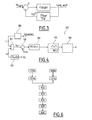
La
Le bus 13 de tension continue fournit une tension Vc, de valeur par exemple égale à 15 kV.The
Le réseau électrique 14 est, par exemple, un réseau alternatif triphasé de tension élevée, typiquement de l'ordre de 33000 V.The
Une charge, 20, par exemple un four à arc, est également reliée au réseau électrique 14.A load, 20, for example an arc furnace, is also connected to the
Le système de conversion 10 de courant comprend un onduleur de tension 18, propre à convertir un courant continu d'entrée en un courant alternatif polyphasé de sortie. Cet onduleur est relié à la source 12 de courant, via le bus de tension continue 13.The current conversion system comprises a
Dans le mode de réalisation considéré, la source de courant 12 comporte un banc de deux condensateurs 32 séparés par un point neutre 33.In the embodiment considered, the
Le courant Iond apparaissant sur la
Le système de conversion 10 comporte également des moyens 22 de commande de l'onduleur 18, adapté pour commander l'onduleur de manière à piloter le courant de sortie délivré par l'onduleur 18 pour chaque phase.The
Le système de conversion 10 comporte également des impédances sur chaque phase, qui sont représentées en
La
Dans le mode de réalisation considéré, le système de conversion 10 est un compensateur d'énergie réactive propre à compenser les variations d'énergie réactive sur le réseau alternatif 14, via la source 12 de courant continu et le bus 13 de tension continue, propres à fournir de l'énergie réactive, en ajustant les phases du courant électrique par rapport à celles de la tension électrique, délivrées sur le réseau.In the embodiment considered, the
L'onduleur de tension 18 comporte une borne positive d'entrée 26A, une borne négative d'entrée 26B, une borne au neutre 33 et M bornes de sortie. Chaque borne de sortie correspond à une phase respective du courant alternatif polyphasé de sortie propre à être délivré par l'onduleur. Le courant de sortie comporte une pluralité M de phases, M étant un nombre entier supérieur ou égal à un.The
Dans l'exemple de réalisation de la
L'onduleur triphasé 18 comprend une borne positive d'entrée 26A, une borne négative d'entrée 26B et trois bornes de sortie 28U, 28V, 28W correspondant chacune à une phase respective U, V, W.The three-
L'onduleur 18 comprend en outre, pour chaque borne de sortie 28U, 28V, 28W, une branche de commutation 30 reliée entre les deux bornes d'entrée 26A, 26B et une branche de clampage 31 reliant le neutre à un point milieu de la branche de commutation associée. En sortie de l'onduleur 18, le courant IondU, IondV, IondW circule sur la phase respectivement, U, V, W.The
La source de tension continue 12 comprend deux condensateurs 32 connectés en série entre les deux bornes d'entrée 26A, 26B, et reliés entre eux en un point milieu 33 formant le neutre.The
En variante, chaque condensateur 32 est remplacé par une source de tension continue.Alternatively, each
Chaque branche de commutation 30 comprend deux interrupteurs électriques commandables 34 connectés en série et dans le même sens, et reliés entre eux par un point milieu, chaque point milieu formant une borne de sortie 28U, 28V, 28W.Each switching
Comme connu en soi, chaque interrupteur électrique 34 est un interrupteur bidirectionnel en courant et unidirectionnel en tension. Chaque interrupteur électrique 34 comprend un transistor 36 et une diode 38 connectée en antiparallèle assurant ainsi des trajets de circulation bidirectionnelle de courant lorsque le transistor 36 est passant.As known per se, each
Tous les interrupteurs électriques 34 sont, par exemple, identiques. Le transistor 36 est, par exemple, un transistor bipolaire à grille isolée, également appelé transistor IGBT (de l'anglais Insulated Gate Bipolar Transistor). La grille de chaque transistor 36 est reliée aux moyens de commande 22 pour recevoir un signal de commande correspondant.All
Chaque branche de clampage 31 est connectée entre le point milieu 33 et une borne de sortie 28U, 28V, 28W. Chaque branche de clampage 31 comporte deux transistors 40 connectés tête-bêche et en série. Elle comporte également deux diodes 42, chacune étant connectée en antiparallèle d'un transistor 40 respectif, assurant ainsi des trajets de circulation bidirectionnelle de courant lorsque le transistor 40 correspondant est passant.Each clamping
Les transistors 40 sont, par exemple, des transistors IGBT.
Entre le système de conversion 10 et le transformateur 24, une inductance 21U, 21V, 21W, est disposée sur respectivement la phase U, V, W.Between the
La charge 20 consomme un courant respectif ICHARGU, ICHARGV, ICHARGW sur la voie respectivement U, V, W.The
Dans le mode de réalisation considéré, les moyens de commande 22 sont adaptés d'une part pour piloter et commander la compensation de la circulation de puissance réactive sur le réseau 14 et ainsi augmenter le facteur de puissance du réseau, et d'autre part pour piloter et commander la réduction des phénomènes de papillotement survenant sur le réseau 14.In the embodiment considered, the control means 22 are adapted on the one hand to drive and control the compensation of the reactive power flow on the
Soit C la valeur de la capacité de la source de tension continue 12 exprimée en Farad, la puissance active Pond (t), fonction du temps t, qui est échangée entre l'onduleur 18 et le réseau 14 sur une phase considérée quelconque U, V ou W, peut être exprimée ainsi : 
où Vc est la tension aux bornes de la source de tension continue 12.Let C be the value of the capacity of the
where V c is the voltage at the terminals of the
En utilisant la transformée de Concordia, puis la transformée de Park, cette équation (1) s'écrit de la manière suivante : 
où Vond est la tension de sortie de l'onduleur dans le repère de Park, et Iond_actif est la composante active courant dans le repère de Park en sortie de l'onduleur 18.Using the Concordia transform, then the Park transform, this equation (1) is written as follows:
where V ond is the output voltage of the inverter in the Park mark, and I ond_active is the current active component in the Park mark at the output of the
En utilisant la transformée de Laplace, l'équation (2) donne : ![]()
où p est l'opérateur de Laplace.Using the Laplace transform, equation (2) gives: ![]()
where p is the Laplace operator.
Dans le système de conversion 10 considéré, le pilotage de la valeur du courant Iond_actif permet de réguler la tension Vc de la source de tension 12. La formule (3) décrit la relation entre le courant actif de l'onduleur Iond_actif et la tension de la source de tension au carré. En contrôlant lond_actif, on contrôle Vc 2 et donc la tension Vc .In the
Pour mettre en oeuvre ce pilotage, on détermine une valeur cible de courant actif en sortie d'onduleur 18 selon l'équation (4) : ![]()
où CDC (p) est la fonction de transfert du régulateur CDC , exprimée à l'aide de la transformation de Lapace, liant la transformée de Laplace du courant Iond_actif (p) et la transformée de Laplace de l'erreur entre le carré de la tension aux bornes de la source de tension continue et une tension de référence de valeur fixée Vref telle qu'on souhaite stabiliser la tension Vc de la source de courant continu 12 à la valeur Vref. To implement this control, an active current target value is determined at the output of ![]()
where C DC ( p ) is the transfer function of the controller C DC , expressed by means of the Lapace transformation, linking the Laplace transform of the current I ond_active ( p ) and the Laplace transform of the error between the square of the voltage at the terminals of the DC voltage source and a reference voltage of fixed value V ref such that it is desired to stabilize the voltage V c of the
Le système linéaire en boucle fermé correspondant aux équations 3 et 4 est représenté en
La fonction de transfert correspondante en boucle ouverte FTBO(p) et la fonction de transfert correspondante en boucle fermée FTBF(p) s'écrivent donc : 
avec 

with
Dans ces formules, Vond est une valeur que l'on peut considérer comme une constante en valeur moyenne. Cette affirmation est vraie car cette équation est développée depuis la formule (2) qui est exprimée dans le repère de Park.In these formulas, V ond is a value that can be considered as a constant in average value. This statement is true because this equation is developed from the formula (2) which is expressed in the Park coordinate system.
La valeur de courant cible Iond_actif déterminée à l'aide de cette boucle de régulation représentée en
Selon l'invention, le régulateur CDC (p) est réglable en fonction de la valeur courante mesurée de la tension Vc . Cette disposition a pour fonction d'assurer une régulation de la tension Vc dans un intervalle fixé de valeurs autour de la valeur Vref , tout en laissant la tension Vc du bus de tension continue 13 fluctuer librement dans cet intervalle. Cette fluctuation a pour effet de diminuer le nombre de manifestations de scintillement dans le réseau 14.According to the invention, the regulator C DC ( p ) is adjustable as a function of the current measured value of the voltage V c . This provision serves to ensure a regulation of the voltage V c in a fixed range of values around the value V ref , while allowing the voltage V c of the
Ainsi, tant que la valeur de la tension Vc est bien à l'intérieur de l'intervalle de fluctuation, le régulateur CDC (p) est très lent, de l'ordre de la seconde. A l'inverse, plus la valeur de la tension approche des bornes de l'intervalle de fluctuation, plus le régulateur CDC (p) est rapide, afin que la valeur de la tension Vc ne sorte pas de l'intervalle de fluctuation.Thus, as long as the value of the voltage V c is indeed within the fluctuation interval, the regulator C DC ( p ) is very slow, of the order of one second. Conversely, the closer the value of the voltage approaches the terminals of the fluctuation interval, the faster the regulator C DC ( p ), so that the value of the voltage V c does not come out of the fluctuation interval .
Dans un mode de réalisation, la formule de CDC (p) est la suivante : 
où K est le terme décrit en (5) qui est constant. C'est KDC qui doit varier en fonction de Vc. Pour augmenter la rapidité du régulateur il faut changer la valeur de CDC(p) et donc de KDC en fonction de Vc. La loi de variation KDC dans la formule (7) est par exemple : Kdc=A*[1+B*f(Vc,Vref)],
où f(Vc,Vref) est une fonction mathématique (fonction valeur absolue, fonction au carré, fonctions linéraires ou non linéaires, etc ...), dont les variables sont Vc et Vref. A et B sont des gains (non variables en fonction de Vc et de Vref) dépendant de plusieurs paramètres du système que l'on souhaite contrôler, comme par exemple la valeur de capacité de stockage du bus DC, la rapidité de commande du compensateur etc ...In one embodiment, the formula of C DC ( p ) is as follows:
where K is the term described in (5) which is constant. It is K DC which must vary according to Vc. To increase the speed of the regulator it is necessary to change the value of C DC (p) and thus of K DC as a function of Vc. The law of variation K DC in the formula (7) is for example: Kdc = A * [1 + B * f ( Vc , V ref )],
where f (V c , V ref ) is a mathematical function (function absolute value, function squared, linear or nonlinear functions, etc ...), whose variables are V c and V ref . A and B are gains (not variable as a function of V c and V ref ) depending on several parameters of the system that one wishes to control, such as for example the storage capacity value of the DC bus, the speed of control of the compensator etc ...
Un tel correcteur CDC(p) est de type proportionnel.Such a corrector C DC (p) is proportional type.
Dans un autre mode de réalisation, la formule de CDC (p) est la suivante : 
où Kidc et Kdc peuvent varier selon plusieurs lois, par exemple : ![]()
![]()
où f(Vc,Vref) est une fonction mathématique (fonction valeur absolue, fonction au carré, fonctions linéraires ou non linéaires, etc ...), dont les variables sont Vc et Vref. A,B,C,D sont des gains dépendant de plusieurs paramètres du système que l'on souhaite contrôler, comme par exemple la valeur de capacité de stockage du bus DC, la rapidité de commande du compensateur etc ...In another embodiment, the formula of C DC ( p ) is as follows:
where K idc and K dc can vary according to several laws, for example: ![]()
![]()
where f (V c , V ref ) is a mathematical function (function absolute value, function squared, linear or nonlinear functions, etc ...), whose variables are V c and V ref . A, B, C, D are gains depending on several parameters of the system that one wishes to control, such as for example the storage capacity value of the DC bus, the speed of control of the compensator, etc.
Un tel correcteur CDC(p) est de type Proportionnel Intégral.Such a corrector C DC (p) is of Proportional Integral type.
Les modules de traitement des moyens de commande 22 adaptés d'une part pour permettre de compenser l'énergie réactive sur le réseau 14 et d'autre part de réduire les problèmes de scintillement, sont décrits en référence à la
On nommera ICHARG et Iond, respectivement le courant dans la charge 20 et le courant délivré par l'onduleur qui sont relatifs à une même phase.I will be named I CHARG and I ond , respectively the current in the
Un bloc de compensation de puissance réactive 50 reçoit en entrée des mesures du courant ICHARG consommé par la charge 20 et est adapté pour mettre en oeuvre un algorithme de détermination d'une valeur cible de courant Ir en sortie de l'onduleur 18 permettant de compenser la puissance réactive de la charge 20 sur la phase considérée.A reactive
Cet algorithme comprend les étapes suivantes :
- Etape 1 : Identifier à partir du courant ICHARG la valeur réactive et active de ce courant. La transformée de Park permet cette identification en séparant les courants sur deux axes en quadratures, qui correspondent aux parties réactive et active du courant mesuré.
- Etape 2 : La totalité du courant réactif identifié est envoyé en tant que référence de composante réactive au sommateur 51.
- Etape 3 : En fonction de la capacité de stockage d'énergie du bus DC, la totalité ou une partie du courant actif identifié à partir du courant ICHARG est envoyé en tant que référence de composante active au sommateur 51.
- Step 1: Identify from current I CHARG the reactive and active value of this current. The Park transform allows this identification by separating the currents on two axes in quadratures, which correspond to the reactive and active parts of the measured current.
- Step 2: The totality of the reactive stream identified is sent as a reactive component reference to the
summator 51. - Step 3: As a function of the energy storage capacity of the DC bus, all or a portion of the active current identified from the current I CHARG is sent as an active component reference to the
adder 51.
Ir correspond donc à la somme de ces deux courants déterminés en ces étapes 2 et 3.Ir corresponds to the sum of these two currents determined in these steps 2 and 3.
Un bloc de régulation 53 reçoit en entrée la valeur courante de la tension aux bornes de la source de tension continue 12.A
Le bloc de régulation 53 est adapté pour déterminer, en fonction de cette valeur, la formule du régulateur à appliquer CDC (p). Le bloc de régulation 53 est adapté pour calculer la valeur cible du courant actif la en sortie de l'onduleur 18, conformément à la formule 4, permettant de réguler la valeur de la tension Vc en diminuant les phénomènes de scintillement.The
Un sommateur 51 est adapté pour sommer les courants cibles Ir et la déterminés par le bloc de compensation de puissance réactive 50 et le bloc de régulation 53 et ainsi déterminer une valeur Iréf de courant cible résultant de cette somme.An
Ce courant Iréf est le courant cible à fournir par l'onduleur sur la phase considérée qui permet la compensation de la charge réactive d'une part et la réduction de problème de scintillement d'autre part.This current I ref is the target current to be supplied by the inverter on the phase in question which allows the compensation of the reactive load on the one hand and the reduction of flicker problem on the other hand.
Un soustracteur 52 permet de calculer la différence entre ce courant cible résultant Iréf et la valeur courante de courant Iond mesurée en sortie de l'onduleur.A
La valeur de cette différence calculée est fournie en entrée d'un régulateur de courant 54. Ce régulateur 54 est propre à calculer, en fonction de la différence calculée, des signaux de tension modulante pour la phase considérée.The value of this calculated difference is provided at the input of a
Ce régulateur est de type PI (Proportionnel Intégral) classiquement utilisé dans la régulation des systèmes bouclés (cf. par exemple http://en.wikipedia.org/wiki/PID controller).This regulator is of type PI (Proportional Integral) conventionally used in the regulation of the looped systems (cf for example http://en.wikipedia.org/wiki/PID controller ).
Ces signaux de tension modulante sont fournis en entrée d'un modulateur 55 adapté pour procéder à une modulation par largeur d'impulsion avec entrelacement des impulsions et déphasage correspondant à la phase considérée (cf http://en.wikipedia.org/wiki/Pulse-width_modulation pour une description générale d'un tel modulateur). Dans une étape, le modulateur est adapté pour comparer une tension modulante reçue en entrée à un signal triangulaire.These modulating voltage signals are provided at the input of a
Les résultats de cette comparaison sont fournis en entrée d'un module de commande 56 propres à déterminer en fonction desdits résultats des signaux de commande destinés aux interrupteurs 34 de la phase considérée et à les appliquer à ces interrupteurs 34.The results of this comparison are provided at the input of a
Sur la
Dans une étape 100a, un courant ICHARG circulant dans la charge 20 du réseau 14, relatif à une phase donnée, est mesuré.In a
Dans une étape 101 a, un courant cible réactif Ir à fournir par l'onduleur 18 est déterminé en fonction du courant circulant dans la charge 20 mesuré.In a
En parallèle de ces étapes 100a, 101 a, dans une étape 100b, un courant Iond circulant en sortie de l'onduleur 18 sur la phase considérée, est mesuré.In parallel with these
Dans une étape 101b, un courant cible actif la à fournir par l'onduleur 18 est déterminé en fonction du courant circulant dans la charge 20 mesuré, tel que décrit ci-dessus à l'aide du régulateur CDC (p), conformément à la formule 4, permettant de réguler la valeur de la tension Vc en diminuant les phénomènes de scintillement.In a
Dans une étape 102, les courants cibles Ir et la sont sommés, le résultat de cette somme déterminant une valeur Iréf de courant cible résultant de cette somme.In a
Ce courant Iréf est le courant cible, à fournir par l'onduleur 18 sur la phase considérée, qui permet la compensation de la charge réactive d'une part et la réduction de problème de scintillement d'autre part.This current I ref is the target current, to be provided by the
Dans une étape 103, la différence entre ce courant cible résultant Iréf et la valeur courante de courant Iond mesurée en sortie de l'onduleur est calculée.In a
Dans une étape 104, des signaux de tension modulante pour la phase considérée sont déterminés, en fonction de la différence calculée, comme décrits plus haut.In a
Dans une étape 105, une modulation par largeur d'impulsion avec entrelacement des impulsions avec déphasage correspondant à la phase considérée est réalisée en fonction de ces signaux de tension modulante, comprenant une opération de comparaison entre une tension modulante et un signal triangulaire.In a
Dans une étape 106, des signaux de commande destinés aux interrupteurs 34 de la phase considérée sont déterminés en fonction des signaux de modulation et appliqués aux interrupteurs 34 de la phase considérée.In a
Les étapes relatives à la compensation de la charge réactive d'une part et à la réduction du papillotement peuvent, suivant les modes de réalisation, être mises en oeuvre séquentiellement ou parallèlement. Dans le cas où cela serait réalisé de façon séquentielle, la composante réactive du courant mesuré Iond est soustraite au courant réactif cible Ir, en vue de déterminer en fonction de cette différence les signaux de commande à appliquer aux commutateurs 34 pour compenser l'énergie réactive de la charge.The steps relating to the compensation of the reactive load on the one hand and to the reduction of the flicker may, depending on the embodiments, be implemented sequentially or in parallel. In the case where this is done sequentially, the reactive component of the measured current I ond is subtracted from the target reactive current Ir, with a view to determining, as a function of this difference, the control signals to be applied to the
De même, la composante active du courant mesuré Iond est soustraite au courant actif cible la, en vue de déterminer en fonction de cette différence, les signaux de commande à appliquer aux commutateurs 34 pour réduire le papillotement sur le réseau.Likewise, the active component of the current measured I ond is subtracted from the target active current la, in order to determine, as a function of this difference, the control signals to be applied to the
L'invention permet donc à la fois de réduire l'apparition de phénomènes de scintillement sur le réseau 14, tout en compensant la puissance réactive de charges sur le réseau.The invention therefore makes it possible at the same time to reduce the appearance of flicker phenomena on the
Claims (8)
caractérisé en ce qu'il comporte en outre des moyens de régulation (22), adaptés pour déterminer une valeur de courant actif cible circulant entre l'onduleur et le réseau propre à réguler la tension courante continue d'entrée (Vc) par rapport à une valeur de référence fixée ;
le dispositif de calcul de signaux de commande des interrupteurs déterminant des signaux de commande en fonction de la valeur dudit courant actif cible déterminée ;
la valeur de courant actif cible étant déterminée à partir de l'erreur entre la valeur de référence et le carré de la tension continue du bus par l'intermédiaire d'une fonction de transfert dont la définition varie en fonction de la valeur courante de ladite tension continue.
characterized in that it further comprises regulating means (22), adapted to determine a target active current value flowing between the inverter and the network adapted to regulate the continuous current input voltage (V c ) relative to a fixed reference value;
the device for calculating control signals of the switches determining control signals as a function of the value of said determined target active current;
the target active current value being determined from the error between the reference value and the square of the DC bus voltage by means of a transfer function whose definition varies according to the current value of said DC voltage.
ou

avec
étant des constantes et f(Vc,Vref) étant une fonction dont les variables d'entrée sont les valeurs courantes de la tension d'entrée Vc et la tension de référence Vref.Reactive energy compensator (10) according to claim 1 or 2, wherein the Laplacian transform of the transfer function C DC (p) is written:
or
with
being constants and f (Vc, Vref) being a function whose input variables are the current values of the input voltage Vc and the reference voltage Vref.
ledit procédé étant caractérisé en ce qu'il comporte les étapes suivantes :
said method being characterized in that it comprises the following steps:
ou

avec
étant des constantes et f(Vc,Vref) étant une fonction dont les variables d'entrée sont les valeurs courantes de la tension d'entrée Vc et la tension de référence Vref.A flicker reduction method according to claim 5 or 6, wherein the Laplacian transform of the transfer function C DC (p) is written:
or
with
being constants and f (Vc, Vref) being a function whose input variables are the current values of the input voltage Vc and the reference voltage Vref.
Applications Claiming Priority (1)
| Application Number | Priority Date | Filing Date | Title |
|---|---|---|---|
| FR1161234A FR2983651B1 (en) | 2011-12-06 | 2011-12-06 | REACTIVE ENERGY COMPENSATOR AND METHOD FOR REDUCING THE ASSOCIATED PAPILLOTE PHENOMENON. |
Publications (2)
| Publication Number | Publication Date |
|---|---|
| EP2602897A1 true EP2602897A1 (en) | 2013-06-12 |
| EP2602897B1 EP2602897B1 (en) | 2014-09-17 |
Family
ID=47263198
Family Applications (1)
| Application Number | Title | Priority Date | Filing Date |
|---|---|---|---|
| EP20120195929 Active EP2602897B1 (en) | 2011-12-06 | 2012-12-06 | Reactive power compensator and method for reducing the associated flickering phenomenon |
Country Status (3)
| Country | Link |
|---|---|
| US (1) | US9197063B2 (en) |
| EP (1) | EP2602897B1 (en) |
| FR (1) | FR2983651B1 (en) |
Families Citing this family (10)
| Publication number | Priority date | Publication date | Assignee | Title |
|---|---|---|---|---|
| US10424935B2 (en) | 2009-09-15 | 2019-09-24 | Rajiv Kumar Varma | Multivariable modulator controller for power generation facility |
| US20150333566A1 (en) * | 2012-09-12 | 2015-11-19 | Schneider Electric It Corporation | A system and method for voltage regulation in a voltage supply |
| US10447073B2 (en) | 2013-01-07 | 2019-10-15 | Schneider Electric It Corporation | Power supply control |
| EP3090315A4 (en) | 2013-12-31 | 2017-08-09 | Schneider Electric IT Corporation | System and methods of grid stabilization |
| US20160158998A1 (en) * | 2014-12-08 | 2016-06-09 | Canon Kabushiki Kaisha | Imprint apparatus and method, and method of manufacturing article |
| WO2016200989A1 (en) * | 2015-06-09 | 2016-12-15 | Renewable Energy Systems Americas Inc. | Method and apparatus for preventing voltage flicker in a power system |
| FR3052308B1 (en) * | 2016-06-06 | 2018-06-15 | Moteurs Leroy-Somer | METHOD FOR CUSTOMIZING THE OPERATION OF AN ALTERNATOR REGULATOR |
| US10910876B2 (en) * | 2016-09-30 | 2021-02-02 | Toshiba Mitsubishi-Electric Industrial Systems Corporation | Uninterruptible power supply device |
| CN114123225B (en) * | 2021-11-19 | 2023-06-30 | 福州大学 | Control method of three-phase reactive power compensator based on double prediction control |
| CN117148709B (en) * | 2023-11-01 | 2024-02-13 | 季华实验室 | Vacuum butterfly valve control method, system, electronic equipment and storage medium |
Citations (3)
| Publication number | Priority date | Publication date | Assignee | Title |
|---|---|---|---|---|
| US6075350A (en) * | 1998-04-24 | 2000-06-13 | Lockheed Martin Energy Research Corporation | Power line conditioner using cascade multilevel inverters for voltage regulation, reactive power correction, and harmonic filtering |
| US20050035815A1 (en) * | 2003-08-13 | 2005-02-17 | Louis Cheng | Active filter for multi-phase ac power system |
| US20060044850A1 (en) * | 2004-08-30 | 2006-03-02 | Uis Abler Electronics Co., Ltd. | Active type harmonic suppression apparatus |
-
2011
- 2011-12-06 FR FR1161234A patent/FR2983651B1/en active Active
-
2012
- 2012-12-06 US US13/706,916 patent/US9197063B2/en active Active
- 2012-12-06 EP EP20120195929 patent/EP2602897B1/en active Active
Patent Citations (3)
| Publication number | Priority date | Publication date | Assignee | Title |
|---|---|---|---|---|
| US6075350A (en) * | 1998-04-24 | 2000-06-13 | Lockheed Martin Energy Research Corporation | Power line conditioner using cascade multilevel inverters for voltage regulation, reactive power correction, and harmonic filtering |
| US20050035815A1 (en) * | 2003-08-13 | 2005-02-17 | Louis Cheng | Active filter for multi-phase ac power system |
| US20060044850A1 (en) * | 2004-08-30 | 2006-03-02 | Uis Abler Electronics Co., Ltd. | Active type harmonic suppression apparatus |
Non-Patent Citations (1)
| Title |
|---|
| H. AKAGI: "Modern active filters and traditional passive filters", BULLETIN OF THE POLISH ACADEMY OF SCIENCES - TECHNICAL SCIENCES, vol. 4, no. 3, 2006 |
Also Published As
| Publication number | Publication date |
|---|---|
| US9197063B2 (en) | 2015-11-24 |
| FR2983651A1 (en) | 2013-06-07 |
| EP2602897B1 (en) | 2014-09-17 |
| FR2983651B1 (en) | 2014-01-03 |
| US20130162049A1 (en) | 2013-06-27 |
Similar Documents
| Publication | Publication Date | Title |
|---|---|---|
| EP2602897B1 (en) | Reactive power compensator and method for reducing the associated flickering phenomenon | |
| EP2613432B1 (en) | Reactive power compensator and associated method for balancing half-bus voltages | |
| EP1655827A1 (en) | Device and method for controlling an energy converter and converter with such device | |
| EP3332474B1 (en) | Virtual capacitance | |
| EP2812974A2 (en) | Control method, control device and mobile electric power storage apparatus | |
| WO2013164249A1 (en) | Nonlinear control device for a dc/dc converter used for conveying hvdc current | |
| EP3591784B1 (en) | Active electrical compensation device | |
| EP2562903B1 (en) | Reactive power compensator comprising N inverters in parallel, N banks of capacitor(s) and a means for connecting the banks via passive electrical components | |
| EP3649728A1 (en) | Converter provided with a module for managing power in an alternating part | |
| Azim et al. | Design of a dynamic phasors‐based droop controller for PV‐based islanded microgrids | |
| EP3539204B1 (en) | Method for controlling a three-phase rectifier for a charging device on board an electric or hybrid vehicle | |
| CA2337388C (en) | Control system adapted to control operation of an ac/dc converter | |
| EP3044865B1 (en) | Command system for an electric charge | |
| EP3520210B1 (en) | Method for controlling a three-phase rectifier for a charging device on board an electrical or hybrid vehicle | |
| Rohten et al. | Discrete nonlinear control based on a double dq transform of a multi-cell UPQC | |
| FR2882475A1 (en) | DEVICE AND METHOD FOR CONTROLLING A CONVERTER AND ELECTRIC CONVERTER COMPRISING SUCH A DEVICE | |
| FR3009771A1 (en) | METHOD FOR CONTROLLING A PERMANENT MAGNET SYNCHRONOUS ELECTRIC MACHINE AND ELECTRONIC CONTROL DEVICE THEREFOR | |
| FR3053854A1 (en) | MODULE FOR CONTROLLING THE INTERNAL ENERGY OF A CONVERTER | |
| EP2582002B1 (en) | Method for controlling the voltage in a grid comprising decentralised sources | |
| Uthayakumar et al. | Sensor fault control scheme for a variable speed wind energy system in a stand‐alone DC micro grid | |
| Hamasaki et al. | A novel method for active filter applying the deadbeat control and the repetitive control | |
| EP1691471A1 (en) | Inverter control apparatus and method thereof | |
| FR3056853B1 (en) | METHOD FOR CONTROLLING A THREE-PHASE RECTIFIER FOR AN ON-BOARD CHARGING DEVICE ON AN ELECTRIC OR HYBRID VEHICLE | |
| US20210104954A1 (en) | Improvements in or relating to the control of voltage source converters | |
| Al Buaijan et al. | Implementation for Controller to Unified Single Phase Power Flow Using Digital Signal Processor (DSP)-TMS320C31 |
Legal Events
| Date | Code | Title | Description |
|---|---|---|---|
| PUAI | Public reference made under article 153(3) epc to a published international application that has entered the european phase |
Free format text: ORIGINAL CODE: 0009012 |
|
| AK | Designated contracting states |
Kind code of ref document: A1 Designated state(s): AL AT BE BG CH CY CZ DE DK EE ES FI FR GB GR HR HU IE IS IT LI LT LU LV MC MK MT NL NO PL PT RO RS SE SI SK SM TR |
|
| AX | Request for extension of the european patent |
Extension state: BA ME |
|
| 17P | Request for examination filed |
Effective date: 20131105 |
|
| RBV | Designated contracting states (corrected) |
Designated state(s): AL AT BE BG CH CY CZ DE DK EE ES FI FR GB GR HR HU IE IS IT LI LT LU LV MC MK MT NL NO PL PT RO RS SE SI SK SM TR |
|
| RIC1 | Information provided on ipc code assigned before grant |
Ipc: H02J 3/16 20060101AFI20131217BHEP Ipc: H02J 3/18 20060101ALI20131217BHEP |
|
| GRAP | Despatch of communication of intention to grant a patent |
Free format text: ORIGINAL CODE: EPIDOSNIGR1 |
|
| INTG | Intention to grant announced |
Effective date: 20140409 |
|
| GRAS | Grant fee paid |
Free format text: ORIGINAL CODE: EPIDOSNIGR3 |
|
| GRAA | (expected) grant |
Free format text: ORIGINAL CODE: 0009210 |
|
| AK | Designated contracting states |
Kind code of ref document: B1 Designated state(s): AL AT BE BG CH CY CZ DE DK EE ES FI FR GB GR HR HU IE IS IT LI LT LU LV MC MK MT NL NO PL PT RO RS SE SI SK SM TR |
|
| REG | Reference to a national code |
Ref country code: GB Ref legal event code: FG4D Free format text: NOT ENGLISH |
|
| REG | Reference to a national code |
Ref country code: CH Ref legal event code: EP |
|
| REG | Reference to a national code |
Ref country code: IE Ref legal event code: FG4D Free format text: LANGUAGE OF EP DOCUMENT: FRENCH |
|
| REG | Reference to a national code |
Ref country code: AT Ref legal event code: REF Ref document number: 688074 Country of ref document: AT Kind code of ref document: T Effective date: 20141015 |
|
| REG | Reference to a national code |
Ref country code: DE Ref legal event code: R096 Ref document number: 602012003141 Country of ref document: DE Effective date: 20141030 |
|
| PG25 | Lapsed in a contracting state [announced via postgrant information from national office to epo] |
Ref country code: NO Free format text: LAPSE BECAUSE OF FAILURE TO SUBMIT A TRANSLATION OF THE DESCRIPTION OR TO PAY THE FEE WITHIN THE PRESCRIBED TIME-LIMIT Effective date: 20141217 Ref country code: GR Free format text: LAPSE BECAUSE OF FAILURE TO SUBMIT A TRANSLATION OF THE DESCRIPTION OR TO PAY THE FEE WITHIN THE PRESCRIBED TIME-LIMIT Effective date: 20141218 Ref country code: SE Free format text: LAPSE BECAUSE OF FAILURE TO SUBMIT A TRANSLATION OF THE DESCRIPTION OR TO PAY THE FEE WITHIN THE PRESCRIBED TIME-LIMIT Effective date: 20140917 Ref country code: LT Free format text: LAPSE BECAUSE OF FAILURE TO SUBMIT A TRANSLATION OF THE DESCRIPTION OR TO PAY THE FEE WITHIN THE PRESCRIBED TIME-LIMIT Effective date: 20140917 Ref country code: FI Free format text: LAPSE BECAUSE OF FAILURE TO SUBMIT A TRANSLATION OF THE DESCRIPTION OR TO PAY THE FEE WITHIN THE PRESCRIBED TIME-LIMIT Effective date: 20140917 |
|
| REG | Reference to a national code |
Ref country code: NL Ref legal event code: VDEP Effective date: 20140917 |
|
| REG | Reference to a national code |
Ref country code: LT Ref legal event code: MG4D |
|
| PG25 | Lapsed in a contracting state [announced via postgrant information from national office to epo] |
Ref country code: RS Free format text: LAPSE BECAUSE OF FAILURE TO SUBMIT A TRANSLATION OF THE DESCRIPTION OR TO PAY THE FEE WITHIN THE PRESCRIBED TIME-LIMIT Effective date: 20140917 Ref country code: HR Free format text: LAPSE BECAUSE OF FAILURE TO SUBMIT A TRANSLATION OF THE DESCRIPTION OR TO PAY THE FEE WITHIN THE PRESCRIBED TIME-LIMIT Effective date: 20140917 Ref country code: LV Free format text: LAPSE BECAUSE OF FAILURE TO SUBMIT A TRANSLATION OF THE DESCRIPTION OR TO PAY THE FEE WITHIN THE PRESCRIBED TIME-LIMIT Effective date: 20140917 Ref country code: CY Free format text: LAPSE BECAUSE OF FAILURE TO SUBMIT A TRANSLATION OF THE DESCRIPTION OR TO PAY THE FEE WITHIN THE PRESCRIBED TIME-LIMIT Effective date: 20140917 |
|
| REG | Reference to a national code |
Ref country code: AT Ref legal event code: MK05 Ref document number: 688074 Country of ref document: AT Kind code of ref document: T Effective date: 20140917 |
|
| PG25 | Lapsed in a contracting state [announced via postgrant information from national office to epo] |
Ref country code: NL Free format text: LAPSE BECAUSE OF FAILURE TO SUBMIT A TRANSLATION OF THE DESCRIPTION OR TO PAY THE FEE WITHIN THE PRESCRIBED TIME-LIMIT Effective date: 20140917 |
|
| PG25 | Lapsed in a contracting state [announced via postgrant information from national office to epo] |
Ref country code: ES Free format text: LAPSE BECAUSE OF FAILURE TO SUBMIT A TRANSLATION OF THE DESCRIPTION OR TO PAY THE FEE WITHIN THE PRESCRIBED TIME-LIMIT Effective date: 20140917 Ref country code: CZ Free format text: LAPSE BECAUSE OF FAILURE TO SUBMIT A TRANSLATION OF THE DESCRIPTION OR TO PAY THE FEE WITHIN THE PRESCRIBED TIME-LIMIT Effective date: 20140917 Ref country code: EE Free format text: LAPSE BECAUSE OF FAILURE TO SUBMIT A TRANSLATION OF THE DESCRIPTION OR TO PAY THE FEE WITHIN THE PRESCRIBED TIME-LIMIT Effective date: 20140917 Ref country code: PT Free format text: LAPSE BECAUSE OF FAILURE TO SUBMIT A TRANSLATION OF THE DESCRIPTION OR TO PAY THE FEE WITHIN THE PRESCRIBED TIME-LIMIT Effective date: 20150119 Ref country code: SK Free format text: LAPSE BECAUSE OF FAILURE TO SUBMIT A TRANSLATION OF THE DESCRIPTION OR TO PAY THE FEE WITHIN THE PRESCRIBED TIME-LIMIT Effective date: 20140917 Ref country code: IS Free format text: LAPSE BECAUSE OF FAILURE TO SUBMIT A TRANSLATION OF THE DESCRIPTION OR TO PAY THE FEE WITHIN THE PRESCRIBED TIME-LIMIT Effective date: 20150117 Ref country code: RO Free format text: LAPSE BECAUSE OF FAILURE TO SUBMIT A TRANSLATION OF THE DESCRIPTION OR TO PAY THE FEE WITHIN THE PRESCRIBED TIME-LIMIT Effective date: 20140917 |
|
| PG25 | Lapsed in a contracting state [announced via postgrant information from national office to epo] |
Ref country code: PL Free format text: LAPSE BECAUSE OF FAILURE TO SUBMIT A TRANSLATION OF THE DESCRIPTION OR TO PAY THE FEE WITHIN THE PRESCRIBED TIME-LIMIT Effective date: 20140917 Ref country code: AT Free format text: LAPSE BECAUSE OF FAILURE TO SUBMIT A TRANSLATION OF THE DESCRIPTION OR TO PAY THE FEE WITHIN THE PRESCRIBED TIME-LIMIT Effective date: 20140917 |
|
| REG | Reference to a national code |
Ref country code: DE Ref legal event code: R097 Ref document number: 602012003141 Country of ref document: DE |
|
| PG25 | Lapsed in a contracting state [announced via postgrant information from national office to epo] |
Ref country code: BE Free format text: LAPSE BECAUSE OF NON-PAYMENT OF DUE FEES Effective date: 20141231 |
|
| PLBE | No opposition filed within time limit |
Free format text: ORIGINAL CODE: 0009261 |
|
| STAA | Information on the status of an ep patent application or granted ep patent |
Free format text: STATUS: NO OPPOSITION FILED WITHIN TIME LIMIT |
|
| PG25 | Lapsed in a contracting state [announced via postgrant information from national office to epo] |
Ref country code: LU Free format text: LAPSE BECAUSE OF FAILURE TO SUBMIT A TRANSLATION OF THE DESCRIPTION OR TO PAY THE FEE WITHIN THE PRESCRIBED TIME-LIMIT Effective date: 20141206 Ref country code: DK Free format text: LAPSE BECAUSE OF FAILURE TO SUBMIT A TRANSLATION OF THE DESCRIPTION OR TO PAY THE FEE WITHIN THE PRESCRIBED TIME-LIMIT Effective date: 20140917 |
|
| 26N | No opposition filed |
Effective date: 20150618 |
|
| PG25 | Lapsed in a contracting state [announced via postgrant information from national office to epo] |
Ref country code: IT Free format text: LAPSE BECAUSE OF FAILURE TO SUBMIT A TRANSLATION OF THE DESCRIPTION OR TO PAY THE FEE WITHIN THE PRESCRIBED TIME-LIMIT Effective date: 20140917 |
|
| REG | Reference to a national code |
Ref country code: IE Ref legal event code: MM4A |
|
| PG25 | Lapsed in a contracting state [announced via postgrant information from national office to epo] |
Ref country code: IE Free format text: LAPSE BECAUSE OF NON-PAYMENT OF DUE FEES Effective date: 20141206 |
|
| PG25 | Lapsed in a contracting state [announced via postgrant information from national office to epo] |
Ref country code: SI Free format text: LAPSE BECAUSE OF FAILURE TO SUBMIT A TRANSLATION OF THE DESCRIPTION OR TO PAY THE FEE WITHIN THE PRESCRIBED TIME-LIMIT Effective date: 20140917 |
|
| REG | Reference to a national code |
Ref country code: FR Ref legal event code: PLFP Year of fee payment: 4 |
|
| PG25 | Lapsed in a contracting state [announced via postgrant information from national office to epo] |
Ref country code: MC Free format text: LAPSE BECAUSE OF FAILURE TO SUBMIT A TRANSLATION OF THE DESCRIPTION OR TO PAY THE FEE WITHIN THE PRESCRIBED TIME-LIMIT Effective date: 20140917 |
|
| PG25 | Lapsed in a contracting state [announced via postgrant information from national office to epo] |
Ref country code: BG Free format text: LAPSE BECAUSE OF FAILURE TO SUBMIT A TRANSLATION OF THE DESCRIPTION OR TO PAY THE FEE WITHIN THE PRESCRIBED TIME-LIMIT Effective date: 20140917 |
|
| PG25 | Lapsed in a contracting state [announced via postgrant information from national office to epo] |
Ref country code: TR Free format text: LAPSE BECAUSE OF FAILURE TO SUBMIT A TRANSLATION OF THE DESCRIPTION OR TO PAY THE FEE WITHIN THE PRESCRIBED TIME-LIMIT Effective date: 20140917 Ref country code: MT Free format text: LAPSE BECAUSE OF FAILURE TO SUBMIT A TRANSLATION OF THE DESCRIPTION OR TO PAY THE FEE WITHIN THE PRESCRIBED TIME-LIMIT Effective date: 20140917 Ref country code: HU Free format text: LAPSE BECAUSE OF FAILURE TO SUBMIT A TRANSLATION OF THE DESCRIPTION OR TO PAY THE FEE WITHIN THE PRESCRIBED TIME-LIMIT; INVALID AB INITIO Effective date: 20121206 |
|
| REG | Reference to a national code |
Ref country code: CH Ref legal event code: PL |
|
| PG25 | Lapsed in a contracting state [announced via postgrant information from national office to epo] |
Ref country code: CH Free format text: LAPSE BECAUSE OF NON-PAYMENT OF DUE FEES Effective date: 20151231 Ref country code: LI Free format text: LAPSE BECAUSE OF NON-PAYMENT OF DUE FEES Effective date: 20151231 |
|
| REG | Reference to a national code |
Ref country code: FR Ref legal event code: PLFP Year of fee payment: 5 |
|
| PG25 | Lapsed in a contracting state [announced via postgrant information from national office to epo] |
Ref country code: SM Free format text: LAPSE BECAUSE OF FAILURE TO SUBMIT A TRANSLATION OF THE DESCRIPTION OR TO PAY THE FEE WITHIN THE PRESCRIBED TIME-LIMIT Effective date: 20140917 |
|
| REG | Reference to a national code |
Ref country code: FR Ref legal event code: PLFP Year of fee payment: 6 |
|
| PG25 | Lapsed in a contracting state [announced via postgrant information from national office to epo] |
Ref country code: MK Free format text: LAPSE BECAUSE OF FAILURE TO SUBMIT A TRANSLATION OF THE DESCRIPTION OR TO PAY THE FEE WITHIN THE PRESCRIBED TIME-LIMIT Effective date: 20140917 |
|
| PG25 | Lapsed in a contracting state [announced via postgrant information from national office to epo] |
Ref country code: AL Free format text: LAPSE BECAUSE OF FAILURE TO SUBMIT A TRANSLATION OF THE DESCRIPTION OR TO PAY THE FEE WITHIN THE PRESCRIBED TIME-LIMIT Effective date: 20140917 |
|
| PGFP | Annual fee paid to national office [announced via postgrant information from national office to epo] |
Ref country code: GB Payment date: 20231121 Year of fee payment: 12 |
|
| PGFP | Annual fee paid to national office [announced via postgrant information from national office to epo] |
Ref country code: FR Payment date: 20231122 Year of fee payment: 12 Ref country code: DE Payment date: 20231121 Year of fee payment: 12 |