EP2543081B1 - Method and apparatus for fabricating monolithically-integrated photovoltaic modules and photovoltaic module - Google Patents
Method and apparatus for fabricating monolithically-integrated photovoltaic modules and photovoltaic module Download PDFInfo
- Publication number
- EP2543081B1 EP2543081B1 EP10707801.6A EP10707801A EP2543081B1 EP 2543081 B1 EP2543081 B1 EP 2543081B1 EP 10707801 A EP10707801 A EP 10707801A EP 2543081 B1 EP2543081 B1 EP 2543081B1
- Authority
- EP
- European Patent Office
- Prior art keywords
- film layer
- area
- photovoltaic
- properties
- deposition
- Prior art date
- Legal status (The legal status is an assumption and is not a legal conclusion. Google has not performed a legal analysis and makes no representation as to the accuracy of the status listed.)
- Active
Links
- 238000000034 method Methods 0.000 title claims description 50
- 238000000151 deposition Methods 0.000 claims description 78
- 230000008021 deposition Effects 0.000 claims description 71
- 239000000463 material Substances 0.000 claims description 65
- 238000000059 patterning Methods 0.000 claims description 44
- 238000004519 manufacturing process Methods 0.000 claims description 23
- 239000000203 mixture Substances 0.000 claims description 18
- 230000002441 reversible effect Effects 0.000 claims description 15
- 229910052802 copper Inorganic materials 0.000 claims description 11
- 230000015556 catabolic process Effects 0.000 claims description 10
- 238000001704 evaporation Methods 0.000 claims description 10
- 230000000737 periodic effect Effects 0.000 claims description 7
- 229910052733 gallium Inorganic materials 0.000 claims description 6
- 230000008020 evaporation Effects 0.000 claims description 5
- 229910052738 indium Inorganic materials 0.000 claims description 5
- 229910052782 aluminium Inorganic materials 0.000 claims description 4
- 229910052711 selenium Inorganic materials 0.000 claims description 4
- 229910052709 silver Inorganic materials 0.000 claims description 4
- 229910052717 sulfur Inorganic materials 0.000 claims description 4
- 229910052729 chemical element Inorganic materials 0.000 claims description 3
- 229910052714 tellurium Inorganic materials 0.000 claims description 2
- 239000010408 film Substances 0.000 description 95
- 239000010949 copper Substances 0.000 description 13
- 230000005693 optoelectronics Effects 0.000 description 12
- 230000008569 process Effects 0.000 description 10
- 230000000875 corresponding effect Effects 0.000 description 8
- 239000010409 thin film Substances 0.000 description 8
- RYGMFSIKBFXOCR-UHFFFAOYSA-N Copper Chemical compound [Cu] RYGMFSIKBFXOCR-UHFFFAOYSA-N 0.000 description 7
- 239000000758 substrate Substances 0.000 description 7
- 230000008901 benefit Effects 0.000 description 6
- 238000010586 diagram Methods 0.000 description 6
- 230000010354 integration Effects 0.000 description 6
- 230000000903 blocking effect Effects 0.000 description 5
- 230000005611 electricity Effects 0.000 description 5
- 239000006096 absorbing agent Substances 0.000 description 4
- 230000006378 damage Effects 0.000 description 4
- 230000002596 correlated effect Effects 0.000 description 3
- 238000005286 illumination Methods 0.000 description 3
- 238000012545 processing Methods 0.000 description 3
- 238000012360 testing method Methods 0.000 description 3
- 229910017612 Cu(In,Ga)Se2 Inorganic materials 0.000 description 2
- 238000004458 analytical method Methods 0.000 description 2
- 230000015572 biosynthetic process Effects 0.000 description 2
- 229910052796 boron Inorganic materials 0.000 description 2
- 229910052799 carbon Inorganic materials 0.000 description 2
- 238000006243 chemical reaction Methods 0.000 description 2
- 239000004020 conductor Substances 0.000 description 2
- 230000007423 decrease Effects 0.000 description 2
- 238000005137 deposition process Methods 0.000 description 2
- 238000013461 design Methods 0.000 description 2
- 230000001747 exhibiting effect Effects 0.000 description 2
- 230000000873 masking effect Effects 0.000 description 2
- 238000005096 rolling process Methods 0.000 description 2
- 239000004065 semiconductor Substances 0.000 description 2
- 238000004513 sizing Methods 0.000 description 2
- 230000007704 transition Effects 0.000 description 2
- 229910004613 CdTe Inorganic materials 0.000 description 1
- ZOKXTWBITQBERF-UHFFFAOYSA-N Molybdenum Chemical compound [Mo] ZOKXTWBITQBERF-UHFFFAOYSA-N 0.000 description 1
- XUIMIQQOPSSXEZ-UHFFFAOYSA-N Silicon Chemical compound [Si] XUIMIQQOPSSXEZ-UHFFFAOYSA-N 0.000 description 1
- 230000004075 alteration Effects 0.000 description 1
- 229910052795 boron group element Inorganic materials 0.000 description 1
- 230000005779 cell damage Effects 0.000 description 1
- 208000037887 cell injury Diseases 0.000 description 1
- 238000006731 degradation reaction Methods 0.000 description 1
- 230000001419 dependent effect Effects 0.000 description 1
- 230000001066 destructive effect Effects 0.000 description 1
- 238000009826 distribution Methods 0.000 description 1
- 230000000694 effects Effects 0.000 description 1
- 238000005516 engineering process Methods 0.000 description 1
- 230000002349 favourable effect Effects 0.000 description 1
- 230000004907 flux Effects 0.000 description 1
- 238000009432 framing Methods 0.000 description 1
- 230000006872 improvement Effects 0.000 description 1
- 238000009413 insulation Methods 0.000 description 1
- 238000001459 lithography Methods 0.000 description 1
- 229910052750 molybdenum Inorganic materials 0.000 description 1
- 239000011733 molybdenum Substances 0.000 description 1
- 238000013021 overheating Methods 0.000 description 1
- 229920000642 polymer Polymers 0.000 description 1
- 238000010248 power generation Methods 0.000 description 1
- 230000001681 protective effect Effects 0.000 description 1
- 230000005855 radiation Effects 0.000 description 1
- 229910052710 silicon Inorganic materials 0.000 description 1
- 239000010703 silicon Substances 0.000 description 1
- 238000005476 soldering Methods 0.000 description 1
- 230000002123 temporal effect Effects 0.000 description 1
- 238000000427 thin-film deposition Methods 0.000 description 1
- 238000009827 uniform distribution Methods 0.000 description 1
Images


Classifications
-
- C—CHEMISTRY; METALLURGY
- C23—COATING METALLIC MATERIAL; COATING MATERIAL WITH METALLIC MATERIAL; CHEMICAL SURFACE TREATMENT; DIFFUSION TREATMENT OF METALLIC MATERIAL; COATING BY VACUUM EVAPORATION, BY SPUTTERING, BY ION IMPLANTATION OR BY CHEMICAL VAPOUR DEPOSITION, IN GENERAL; INHIBITING CORROSION OF METALLIC MATERIAL OR INCRUSTATION IN GENERAL
- C23C—COATING METALLIC MATERIAL; COATING MATERIAL WITH METALLIC MATERIAL; SURFACE TREATMENT OF METALLIC MATERIAL BY DIFFUSION INTO THE SURFACE, BY CHEMICAL CONVERSION OR SUBSTITUTION; COATING BY VACUUM EVAPORATION, BY SPUTTERING, BY ION IMPLANTATION OR BY CHEMICAL VAPOUR DEPOSITION, IN GENERAL
- C23C14/00—Coating by vacuum evaporation, by sputtering or by ion implantation of the coating forming material
- C23C14/06—Coating by vacuum evaporation, by sputtering or by ion implantation of the coating forming material characterised by the coating material
- C23C14/0623—Sulfides, selenides or tellurides
-
- C—CHEMISTRY; METALLURGY
- C23—COATING METALLIC MATERIAL; COATING MATERIAL WITH METALLIC MATERIAL; CHEMICAL SURFACE TREATMENT; DIFFUSION TREATMENT OF METALLIC MATERIAL; COATING BY VACUUM EVAPORATION, BY SPUTTERING, BY ION IMPLANTATION OR BY CHEMICAL VAPOUR DEPOSITION, IN GENERAL; INHIBITING CORROSION OF METALLIC MATERIAL OR INCRUSTATION IN GENERAL
- C23C—COATING METALLIC MATERIAL; COATING MATERIAL WITH METALLIC MATERIAL; SURFACE TREATMENT OF METALLIC MATERIAL BY DIFFUSION INTO THE SURFACE, BY CHEMICAL CONVERSION OR SUBSTITUTION; COATING BY VACUUM EVAPORATION, BY SPUTTERING, BY ION IMPLANTATION OR BY CHEMICAL VAPOUR DEPOSITION, IN GENERAL
- C23C14/00—Coating by vacuum evaporation, by sputtering or by ion implantation of the coating forming material
- C23C14/22—Coating by vacuum evaporation, by sputtering or by ion implantation of the coating forming material characterised by the process of coating
- C23C14/24—Vacuum evaporation
-
- C—CHEMISTRY; METALLURGY
- C23—COATING METALLIC MATERIAL; COATING MATERIAL WITH METALLIC MATERIAL; CHEMICAL SURFACE TREATMENT; DIFFUSION TREATMENT OF METALLIC MATERIAL; COATING BY VACUUM EVAPORATION, BY SPUTTERING, BY ION IMPLANTATION OR BY CHEMICAL VAPOUR DEPOSITION, IN GENERAL; INHIBITING CORROSION OF METALLIC MATERIAL OR INCRUSTATION IN GENERAL
- C23C—COATING METALLIC MATERIAL; COATING MATERIAL WITH METALLIC MATERIAL; SURFACE TREATMENT OF METALLIC MATERIAL BY DIFFUSION INTO THE SURFACE, BY CHEMICAL CONVERSION OR SUBSTITUTION; COATING BY VACUUM EVAPORATION, BY SPUTTERING, BY ION IMPLANTATION OR BY CHEMICAL VAPOUR DEPOSITION, IN GENERAL
- C23C14/00—Coating by vacuum evaporation, by sputtering or by ion implantation of the coating forming material
- C23C14/22—Coating by vacuum evaporation, by sputtering or by ion implantation of the coating forming material characterised by the process of coating
- C23C14/54—Controlling or regulating the coating process
- C23C14/548—Controlling the composition
-
- C—CHEMISTRY; METALLURGY
- C23—COATING METALLIC MATERIAL; COATING MATERIAL WITH METALLIC MATERIAL; CHEMICAL SURFACE TREATMENT; DIFFUSION TREATMENT OF METALLIC MATERIAL; COATING BY VACUUM EVAPORATION, BY SPUTTERING, BY ION IMPLANTATION OR BY CHEMICAL VAPOUR DEPOSITION, IN GENERAL; INHIBITING CORROSION OF METALLIC MATERIAL OR INCRUSTATION IN GENERAL
- C23C—COATING METALLIC MATERIAL; COATING MATERIAL WITH METALLIC MATERIAL; SURFACE TREATMENT OF METALLIC MATERIAL BY DIFFUSION INTO THE SURFACE, BY CHEMICAL CONVERSION OR SUBSTITUTION; COATING BY VACUUM EVAPORATION, BY SPUTTERING, BY ION IMPLANTATION OR BY CHEMICAL VAPOUR DEPOSITION, IN GENERAL
- C23C14/00—Coating by vacuum evaporation, by sputtering or by ion implantation of the coating forming material
- C23C14/22—Coating by vacuum evaporation, by sputtering or by ion implantation of the coating forming material characterised by the process of coating
- C23C14/56—Apparatus specially adapted for continuous coating; Arrangements for maintaining the vacuum, e.g. vacuum locks
- C23C14/562—Apparatus specially adapted for continuous coating; Arrangements for maintaining the vacuum, e.g. vacuum locks for coating elongated substrates
-
- H—ELECTRICITY
- H01—ELECTRIC ELEMENTS
- H01L—SEMICONDUCTOR DEVICES NOT COVERED BY CLASS H10
- H01L31/00—Semiconductor devices sensitive to infrared radiation, light, electromagnetic radiation of shorter wavelength or corpuscular radiation and specially adapted either for the conversion of the energy of such radiation into electrical energy or for the control of electrical energy by such radiation; Processes or apparatus specially adapted for the manufacture or treatment thereof or of parts thereof; Details thereof
- H01L31/0248—Semiconductor devices sensitive to infrared radiation, light, electromagnetic radiation of shorter wavelength or corpuscular radiation and specially adapted either for the conversion of the energy of such radiation into electrical energy or for the control of electrical energy by such radiation; Processes or apparatus specially adapted for the manufacture or treatment thereof or of parts thereof; Details thereof characterised by their semiconductor bodies
- H01L31/0256—Semiconductor devices sensitive to infrared radiation, light, electromagnetic radiation of shorter wavelength or corpuscular radiation and specially adapted either for the conversion of the energy of such radiation into electrical energy or for the control of electrical energy by such radiation; Processes or apparatus specially adapted for the manufacture or treatment thereof or of parts thereof; Details thereof characterised by their semiconductor bodies characterised by the material
- H01L31/0264—Inorganic materials
- H01L31/032—Inorganic materials including, apart from doping materials or other impurities, only compounds not provided for in groups H01L31/0272 - H01L31/0312
- H01L31/0322—Inorganic materials including, apart from doping materials or other impurities, only compounds not provided for in groups H01L31/0272 - H01L31/0312 comprising only AIBIIICVI chalcopyrite compounds, e.g. Cu In Se2, Cu Ga Se2, Cu In Ga Se2
-
- H—ELECTRICITY
- H01—ELECTRIC ELEMENTS
- H01L—SEMICONDUCTOR DEVICES NOT COVERED BY CLASS H10
- H01L31/00—Semiconductor devices sensitive to infrared radiation, light, electromagnetic radiation of shorter wavelength or corpuscular radiation and specially adapted either for the conversion of the energy of such radiation into electrical energy or for the control of electrical energy by such radiation; Processes or apparatus specially adapted for the manufacture or treatment thereof or of parts thereof; Details thereof
- H01L31/04—Semiconductor devices sensitive to infrared radiation, light, electromagnetic radiation of shorter wavelength or corpuscular radiation and specially adapted either for the conversion of the energy of such radiation into electrical energy or for the control of electrical energy by such radiation; Processes or apparatus specially adapted for the manufacture or treatment thereof or of parts thereof; Details thereof adapted as photovoltaic [PV] conversion devices
- H01L31/042—PV modules or arrays of single PV cells
- H01L31/044—PV modules or arrays of single PV cells including bypass diodes
- H01L31/0443—PV modules or arrays of single PV cells including bypass diodes comprising bypass diodes integrated or directly associated with the devices, e.g. bypass diodes integrated or formed in or on the same substrate as the photovoltaic cells
-
- H—ELECTRICITY
- H01—ELECTRIC ELEMENTS
- H01L—SEMICONDUCTOR DEVICES NOT COVERED BY CLASS H10
- H01L31/00—Semiconductor devices sensitive to infrared radiation, light, electromagnetic radiation of shorter wavelength or corpuscular radiation and specially adapted either for the conversion of the energy of such radiation into electrical energy or for the control of electrical energy by such radiation; Processes or apparatus specially adapted for the manufacture or treatment thereof or of parts thereof; Details thereof
- H01L31/04—Semiconductor devices sensitive to infrared radiation, light, electromagnetic radiation of shorter wavelength or corpuscular radiation and specially adapted either for the conversion of the energy of such radiation into electrical energy or for the control of electrical energy by such radiation; Processes or apparatus specially adapted for the manufacture or treatment thereof or of parts thereof; Details thereof adapted as photovoltaic [PV] conversion devices
- H01L31/042—PV modules or arrays of single PV cells
- H01L31/0445—PV modules or arrays of single PV cells including thin film solar cells, e.g. single thin film a-Si, CIS or CdTe solar cells
- H01L31/046—PV modules composed of a plurality of thin film solar cells deposited on the same substrate
- H01L31/0463—PV modules composed of a plurality of thin film solar cells deposited on the same substrate characterised by special patterning methods to connect the PV cells in a module, e.g. laser cutting of the conductive or active layers
-
- H—ELECTRICITY
- H01—ELECTRIC ELEMENTS
- H01L—SEMICONDUCTOR DEVICES NOT COVERED BY CLASS H10
- H01L31/00—Semiconductor devices sensitive to infrared radiation, light, electromagnetic radiation of shorter wavelength or corpuscular radiation and specially adapted either for the conversion of the energy of such radiation into electrical energy or for the control of electrical energy by such radiation; Processes or apparatus specially adapted for the manufacture or treatment thereof or of parts thereof; Details thereof
- H01L31/04—Semiconductor devices sensitive to infrared radiation, light, electromagnetic radiation of shorter wavelength or corpuscular radiation and specially adapted either for the conversion of the energy of such radiation into electrical energy or for the control of electrical energy by such radiation; Processes or apparatus specially adapted for the manufacture or treatment thereof or of parts thereof; Details thereof adapted as photovoltaic [PV] conversion devices
- H01L31/06—Semiconductor devices sensitive to infrared radiation, light, electromagnetic radiation of shorter wavelength or corpuscular radiation and specially adapted either for the conversion of the energy of such radiation into electrical energy or for the control of electrical energy by such radiation; Processes or apparatus specially adapted for the manufacture or treatment thereof or of parts thereof; Details thereof adapted as photovoltaic [PV] conversion devices characterised by at least one potential-jump barrier or surface barrier
- H01L31/072—Semiconductor devices sensitive to infrared radiation, light, electromagnetic radiation of shorter wavelength or corpuscular radiation and specially adapted either for the conversion of the energy of such radiation into electrical energy or for the control of electrical energy by such radiation; Processes or apparatus specially adapted for the manufacture or treatment thereof or of parts thereof; Details thereof adapted as photovoltaic [PV] conversion devices characterised by at least one potential-jump barrier or surface barrier the potential barriers being only of the PN heterojunction type
- H01L31/073—Semiconductor devices sensitive to infrared radiation, light, electromagnetic radiation of shorter wavelength or corpuscular radiation and specially adapted either for the conversion of the energy of such radiation into electrical energy or for the control of electrical energy by such radiation; Processes or apparatus specially adapted for the manufacture or treatment thereof or of parts thereof; Details thereof adapted as photovoltaic [PV] conversion devices characterised by at least one potential-jump barrier or surface barrier the potential barriers being only of the PN heterojunction type comprising only AIIBVI compound semiconductors, e.g. CdS/CdTe solar cells
-
- H—ELECTRICITY
- H01—ELECTRIC ELEMENTS
- H01L—SEMICONDUCTOR DEVICES NOT COVERED BY CLASS H10
- H01L31/00—Semiconductor devices sensitive to infrared radiation, light, electromagnetic radiation of shorter wavelength or corpuscular radiation and specially adapted either for the conversion of the energy of such radiation into electrical energy or for the control of electrical energy by such radiation; Processes or apparatus specially adapted for the manufacture or treatment thereof or of parts thereof; Details thereof
- H01L31/04—Semiconductor devices sensitive to infrared radiation, light, electromagnetic radiation of shorter wavelength or corpuscular radiation and specially adapted either for the conversion of the energy of such radiation into electrical energy or for the control of electrical energy by such radiation; Processes or apparatus specially adapted for the manufacture or treatment thereof or of parts thereof; Details thereof adapted as photovoltaic [PV] conversion devices
- H01L31/06—Semiconductor devices sensitive to infrared radiation, light, electromagnetic radiation of shorter wavelength or corpuscular radiation and specially adapted either for the conversion of the energy of such radiation into electrical energy or for the control of electrical energy by such radiation; Processes or apparatus specially adapted for the manufacture or treatment thereof or of parts thereof; Details thereof adapted as photovoltaic [PV] conversion devices characterised by at least one potential-jump barrier or surface barrier
- H01L31/072—Semiconductor devices sensitive to infrared radiation, light, electromagnetic radiation of shorter wavelength or corpuscular radiation and specially adapted either for the conversion of the energy of such radiation into electrical energy or for the control of electrical energy by such radiation; Processes or apparatus specially adapted for the manufacture or treatment thereof or of parts thereof; Details thereof adapted as photovoltaic [PV] conversion devices characterised by at least one potential-jump barrier or surface barrier the potential barriers being only of the PN heterojunction type
- H01L31/0749—Semiconductor devices sensitive to infrared radiation, light, electromagnetic radiation of shorter wavelength or corpuscular radiation and specially adapted either for the conversion of the energy of such radiation into electrical energy or for the control of electrical energy by such radiation; Processes or apparatus specially adapted for the manufacture or treatment thereof or of parts thereof; Details thereof adapted as photovoltaic [PV] conversion devices characterised by at least one potential-jump barrier or surface barrier the potential barriers being only of the PN heterojunction type including a AIBIIICVI compound, e.g. CdS/CulnSe2 [CIS] heterojunction solar cells
-
- H—ELECTRICITY
- H01—ELECTRIC ELEMENTS
- H01L—SEMICONDUCTOR DEVICES NOT COVERED BY CLASS H10
- H01L31/00—Semiconductor devices sensitive to infrared radiation, light, electromagnetic radiation of shorter wavelength or corpuscular radiation and specially adapted either for the conversion of the energy of such radiation into electrical energy or for the control of electrical energy by such radiation; Processes or apparatus specially adapted for the manufacture or treatment thereof or of parts thereof; Details thereof
- H01L31/18—Processes or apparatus specially adapted for the manufacture or treatment of these devices or of parts thereof
- H01L31/1828—Processes or apparatus specially adapted for the manufacture or treatment of these devices or of parts thereof the active layers comprising only AIIBVI compounds, e.g. CdS, ZnS, CdTe
- H01L31/1836—Processes or apparatus specially adapted for the manufacture or treatment of these devices or of parts thereof the active layers comprising only AIIBVI compounds, e.g. CdS, ZnS, CdTe comprising a growth substrate not being an AIIBVI compound
-
- H—ELECTRICITY
- H01—ELECTRIC ELEMENTS
- H01L—SEMICONDUCTOR DEVICES NOT COVERED BY CLASS H10
- H01L21/00—Processes or apparatus adapted for the manufacture or treatment of semiconductor or solid state devices or of parts thereof
- H01L21/02—Manufacture or treatment of semiconductor devices or of parts thereof
- H01L21/02104—Forming layers
- H01L21/02365—Forming inorganic semiconducting materials on a substrate
- H01L21/02518—Deposited layers
- H01L21/02521—Materials
- H01L21/02568—Chalcogenide semiconducting materials not being oxides, e.g. ternary compounds
-
- Y—GENERAL TAGGING OF NEW TECHNOLOGICAL DEVELOPMENTS; GENERAL TAGGING OF CROSS-SECTIONAL TECHNOLOGIES SPANNING OVER SEVERAL SECTIONS OF THE IPC; TECHNICAL SUBJECTS COVERED BY FORMER USPC CROSS-REFERENCE ART COLLECTIONS [XRACs] AND DIGESTS
- Y02—TECHNOLOGIES OR APPLICATIONS FOR MITIGATION OR ADAPTATION AGAINST CLIMATE CHANGE
- Y02E—REDUCTION OF GREENHOUSE GAS [GHG] EMISSIONS, RELATED TO ENERGY GENERATION, TRANSMISSION OR DISTRIBUTION
- Y02E10/00—Energy generation through renewable energy sources
- Y02E10/50—Photovoltaic [PV] energy
- Y02E10/541—CuInSe2 material PV cells
-
- Y—GENERAL TAGGING OF NEW TECHNOLOGICAL DEVELOPMENTS; GENERAL TAGGING OF CROSS-SECTIONAL TECHNOLOGIES SPANNING OVER SEVERAL SECTIONS OF THE IPC; TECHNICAL SUBJECTS COVERED BY FORMER USPC CROSS-REFERENCE ART COLLECTIONS [XRACs] AND DIGESTS
- Y02—TECHNOLOGIES OR APPLICATIONS FOR MITIGATION OR ADAPTATION AGAINST CLIMATE CHANGE
- Y02E—REDUCTION OF GREENHOUSE GAS [GHG] EMISSIONS, RELATED TO ENERGY GENERATION, TRANSMISSION OR DISTRIBUTION
- Y02E10/00—Energy generation through renewable energy sources
- Y02E10/50—Photovoltaic [PV] energy
- Y02E10/543—Solar cells from Group II-VI materials
-
- Y—GENERAL TAGGING OF NEW TECHNOLOGICAL DEVELOPMENTS; GENERAL TAGGING OF CROSS-SECTIONAL TECHNOLOGIES SPANNING OVER SEVERAL SECTIONS OF THE IPC; TECHNICAL SUBJECTS COVERED BY FORMER USPC CROSS-REFERENCE ART COLLECTIONS [XRACs] AND DIGESTS
- Y02—TECHNOLOGIES OR APPLICATIONS FOR MITIGATION OR ADAPTATION AGAINST CLIMATE CHANGE
- Y02P—CLIMATE CHANGE MITIGATION TECHNOLOGIES IN THE PRODUCTION OR PROCESSING OF GOODS
- Y02P70/00—Climate change mitigation technologies in the production process for final industrial or consumer products
- Y02P70/50—Manufacturing or production processes characterised by the final manufactured product
Definitions
- the invention relates to a method and apparatus for fabricating monolithically-integrated photovoltaic modules, according to claims 1 and 9.
- the invention also relates to a photovoltaic module according to claim 10.
- the method comprises the steps of forming a film layer on a deposition area such that at least a portion of said film layer constitutes a photoactive layer, applying a patterning scheme for dividing said film layer into area sections and providing electrically interconnected components, each comprising at least one of said area sections.
- the photovoltaic module comprises at least one film layer, said film layer being divided into area sections, and electrically interconnected components, each comprising at least one of said area sections.
- the invention relates to the fabrication of photovoltaic modules with a film layer formed by, but not limited to, an ABC 2 material, wherein A represents elements in group 11 of the periodic table of chemical elements as defined by the International Union of Pure and Applied Chemistry including Cu or Ag, B represents elements in group 13 of the periodic table including In, Ga, or Al, and C represents elements in group 16 of the periodic table including S, Se, or Te.
- ABC 2 material wherein A represents elements in group 11 of the periodic table of chemical elements as defined by the International Union of Pure and Applied Chemistry including Cu or Ag, B represents elements in group 13 of the periodic table including In, Ga, or Al, and C represents elements in group 16 of the periodic table including S, Se, or Te.
- Thin-film photovoltaic cells such as Cu(In,Ga)Se 2 - (CIGS-) or CdTe-based photovoltaic cells show a high potential for cheaper solar electricity, lower energy payback time, and improved life cycle impact as compared to traditional wafer-based silicon photovoltaic cells. These advantages originate mostly from three factors: First, thin-film absorbers can absorb solar radiation within very thin layers of the order of micrometers. Second, thin-film photovoltaic modules can be produced in-line and in large sizes with a high degree of automation and thus little labor cost. Third, thin-film photovoltaic cells can be monolithically integrated to photovoltaic modules.
- Such a photovoltaic module essentially consists of an array of interconnected photovoltaic cells and optional additional devices such as bypass diodes, directly or indirectly connected to current collectors (busbars) and on, or in between, supporting structures for protective and/or mechanical reasons.
- the term "monolithical integration" means that several photovoltaic cells on the same substrate can be interconnected during manufacturing to form a module on that substrate, whereas non-monolithically-integrated modules (such as wafer-based modules) consist of individual photovoltaic cells requiring manual interconnection after cell manufacturing.
- photovoltaic module films need to be patterned in one or several processing steps at one or different stages of the manufacturing process, either during or after the deposition of individual layers or during or after deposition of groups of layers,see for example M. Powalla and D. Bonnet, Advances in OptoElectronics, vol. 2007, Article ID 97545, 2007 .
- Patterning is usually achieved by applying a predefined patterning scheme in order to divide the photoactive film layer and/or auxiliary layers, e.g. back contact, absorber, buffer, window, and front contact layers, in several area sections for defining location, size, and shape of module elements, in particular photovoltaic cells.
- Patterning is further performed such that at least two interconnects can be formed to each module element - typically to each element's plus and minus pole, respectively - such that the element is connected either in parallel or in series to other, typically adjacent, module elements or to the busbar.
- Common patterning techniques are scribing methods such as mechanical or laser scribing of one or several layers at a time, but also shadowing, lithography, or other methods are used, as described for example in WO 03/061013 A1 .
- Monolithic integration can also be achieved by structuring certain layers during their deposition e.g. by using shadow masks.
- Each photovoltaic cell has a maximum power point (MPP), which denotes the condition of a cell, under which it delivers the highest amount of electrical power under given illumination conditions.
- MPP maximum power point
- a large photovoltaic cell can be thought of as a submodule consisting of the parallel connection of smaller cells which together cover the same area as the large cell. As soon as the voltage across this submodule exceeds the diode threshold voltage of one of the smaller cells, the current produced by the other cells starts to flow back through that cell with the lowest diode threshold voltage. Hence, cells with a high MPP voltage cannot be operated at that voltage without losing too much current due to current reversal.
- the MPP voltage of the submodule is dragged towards the MPP voltage of the cell with the lowest diode threshold voltage. If the differences in MPP voltage between the small cells are large, many cells are operated below their MPP, thereby reducing submodule efficiency. In the extreme case, owing to the presence of one weak cell, all other cells connected in parallel may operate at non-optimum efficiency in order to operate the submodule at its MPP. Therefore, it is highly desirable that any photovoltaic cell possess homogeneous optoelectronic properties across its area in order to deliver maximum electrical power.
- a reverse bias protection can be employed, e.g.
- bypass diode In the form of a bypass diode: When a negative bias voltage builds up across a photovoltaic cell and the threshold voltage of the bypass diode is exceeded, then reverse current can flow through the bypass diode instead of through the weak spot of the weakest or shaded cell, provided that the threshold voltage of the bypass diode is lower than the reverse-breakdown voltage of the photovoltaic cell's weak spot.
- Bypass diodes can be incorporated into monolithically-integrated thin-film modules by connecting photovoltaic cells anti-parallel, i.e. with their polarities reversed.
- the diodes can be formed over single cells, lower- and higher-level submodules consisting of several cells, and also over the whole module, to another cell or to a string of other cells.
- These diodes traditionally have been discrete components attached to the photovoltaic module by soldering or similar techniques.
- Another technique for creating integrated diodes includes adding additional layers non-monolithically onto the bottom or surface of the cell, as described for example in U.S. patent no. US 6,635,507 .
- a diode can also be formed by monolithic integration into the module as described in patent no. US 6,690,041 .
- each of the described components of a photovoltaic module i.e. photovoltaic cells, submodules, bypass diodes, etc.
- photovoltaic cells, submodules, bypass diodes, etc. are ordinarily described by one or several characteristic values of their respective current-voltage characteristic curves.
- the open-circuit voltage and/or the current/voltage at the maximum power point are often quoted with respect to photovoltaic cell or photovoltaic submodule properties.
- a diode behavior is generally well described by the value of the threshold voltage.
- the reverse breakdown voltage is a characteristic value.
- WO 2008/042682 A2 describes a thin film photovoltaic module, in which an undesired non-uniformity of the film layer shall be compensated.
- the module is divided into single photovoltaic cells along the direction, in which the non-uniformity of the film layer occurs.
- such a division can also be carried out within several submodules of the module, wherein corresponding submodules in an area zone of a given film-layer uniformity are series connected to a set of submodules, and these different sets of submodules are mutually connected in parallel.
- protect diodes are fabricated on the film layer as a part of the lithographic process during which adjacent photovoltaic cells are connected.
- the protect diodes are arranged in parallel to the direction, in which the film layer is divided into single photovoltaic cells, such that they are fabricated from the same film layer properties as the photovoltaic cells. This has the disadvantage that deviating film properties, which may be required for a reliable functionality of these additional components, are not inherently accounted for, and additional processing steps may be required to improve their performance.
- the invention suggests that at least one compositional and/or structural property, in particular material percentage composition and/or thickness, of said film layer is varied over said deposition area and said patterning scheme is applied in such a way that at least one of said film layer variations in at least one of said area sections is reduced with respect to the corresponding film layer variation over said deposition area.
- at least two of said area sections are provided with substantially differing compositional and/or structural properties such that at least two of said components exhibit substantially differing current-voltage characteristics.
- said at least two components are interconnected in parallel for exploiting at least one advantage of said differing current-voltage characteristics:
- One of the advantages may arise from the possibility of voltage matching of at least two components consisting of single photovoltaic cells or submodules, each comprising several photovoltaic cells in a series connection, wherein said different current-voltage characteristics may comprise a different current value at a substantially equal voltage value at the maximum power point and/or a different open circuit voltage of these components.
- Another advantage may include the possibility of a simplified monolithic integration process of additional components, in particular bypass diodes, resistors and/or Zener diodes, wherein said different current-voltage characteristics may comprise a different diode threshold voltage and/or a different reverse breakdown voltage.
- said current-voltage characteristics of at least two of said components may differ by a factor of at least 2 percent, more preferred by a factor of at least 5 percent, and most preferred by a factor of at least 10 percent.
- compositional and/or structural property of said film layer may occur or be imposed over said deposition area.
- said compositional and/or structural and/or voltage properties may comprise the material percentage composition and/or the thickness of said film layer.
- film patterning processes may be correlated with spatial variations of film properties such as electronic, compositional, optoelectronic, or structural properties.
- this correlation of patterning with spatial variations of film properties may be exploited to tailor photovoltaic cell patterns and geometries such that each individual photovoltaic cell exhibits comparable photovoltaic properties and consequently good current and voltage matching can be achieved.
- the lifetime electricity generation of the module may be maximized and/or the temporal power output profile of the module may be optimized, while at the same time conditions and restrictions on thin-film deposition processes can be relaxed and/or material utilization yield during the deposition process may be improved.
- said correlation of patterning with spatial film variations may be exploited for creating further tailored units such as bypass diodes, resistances, or conductors. The aforementioned benefits may therefore advantageously contribute to a decrease of the cost of solar electricity generation.
- such a tailoring of photovoltaic cell patterns may be achieved by applying said patterning scheme in such a way that at least one geometrical property, in particular the size and/or shape and/or orientation and/or areal number, of said area sections is varied in dependence of at least one of said film layer variations.
- at least one geometrical property in particular the size and/or shape and/or orientation and/or areal number, of said area sections is varied in dependence of at least one of said film layer variations.
- single photovoltaic cells and/or submodules each comprising several photovoltaic cells in a series connection, may be provided with a substantially equal voltage value at their maximum power point.
- said patterning scheme may be applied in such a way as to subdivide said deposition area into area zones with different compositional and/or structural properties of said film layer, at least one of said area zones comprising area sections with essentially the same compositional and/or structural properties of said film layer.
- At least one of said components in at least one area zone may be provided by a submodule, each comprising several single photovoltaic cells in a series connection.
- said method may comprise the further steps of determining at least one of said film layer variations and adjusting said patterning scheme in dependence thereof.
- this step may comprise measuring of local properties of said film layer by means of non-destructive tests.
- said determination of at least one of said film layer variations may be based on empirical values and/or based on theoretical calculations and/or performed by testing of prior batches and/or by testing of periodic zones of said film layer, in particular of sacrificial zones, etc.
- At least one of said area sections with a larger size may be arranged in a region where said film layer variations are small as compared to at least one of said area sections with a smaller size that is arranged in a region where the corresponding film layer variations are larger.
- said patterning scheme may be applied such that the local single photovoltaic cell current-voltage characteristics in at least one submodule is reduced with respect to local photovoltaic cell current-voltage characteristics of another submodule by a factor of at least 2 percent, more preferred by a factor of at least 5 percent and most preferred by a factor of at least 10 percent.
- said application of said patterning scheme may subdivide the photovoltaic module into zones of improved homogeneity of photovoltaic properties such that particularly the voltage at the maximum power point (MPP) in the predominant zone is increased by at least the open circuit voltage of a photovoltaic cell thus created in the zone of lower open circuit voltage properties.
- MPP maximum power point
- said forming of a film layer comprises the steps of evaporating and depositing material on said deposition area from at least one material source, wherein said deposition area is moved with respect to said material source and said varying of at least one compositional and/or structural property of said film layer is carried out transverse to the respective moving direction.
- a continuous manufacturing process may be provided by varying said compositional and/or structural property in at least one or two dimensions and by moving said deposition area in a different direction.
- Such a method may be integrated in a so called roll-to-roll manufacturing technology for allowing continuous deposition of said film layer at high speeds under rolling of said deposition area.
- said deposition area may be constituted by a plastic substrate.
- At least two, more preferred at least three, of said area sections may be disposed in a transverse direction with respect to said moving direction.
- area sections with a larger size may be provided at a center portion of said deposition area with respect to said transverse direction as compared to area sections located at a side portion.
- said area sections at said center portion may cover at least two times, more preferred at least three times, more space in that transverse direction as compared to said area sections at said side portion.
- said forming of a film layer comprises evaporating and depositing materials on said deposition area from separated material sources, wherein the deposition rate of at least one of said sources is varied over said deposition area such that said varying of compositional properties comprises varying of a percentage composition and/or an absolute quantity of at least one of said deposited materials.
- said varying of compositional properties comprises varying of a percentage composition and/or an absolute quantity of at least one of said deposited materials.
- Said at least one source may be a point source or a linear source, wherein also sources of any other shape or nature are conceivable.
- said film variations may be produced by an inhomogeneous deposition profile of said source with respect to said deposition area, which results in variations of the deposition rate on said deposition area.
- the local deposition rate on said deposition area may vary with distance and angle from the part of said source or sources at which material is leaving the source or sources.
- said local deposition rates may vary from said source or sources by a Lambert-cosine law or with a similar behavior.
- deposition-source profiles may be adapted and correlated with suitable cell structuring patterns, such as to improve the optoelectronic properties of photovoltaic cells, bypass diodes, resistances, Zener diodes or conductors.
- means to control deposition in particular shielding means and/or masking means and/or material guiding means, are applied on or in the vicinity of said material source or sources to control at least one of said film layer variations.
- adequate control of said deposition rate combined with appropriate application of said patterning scheme may be used to optimize the output power of said module, in particular with respect to full illumination conditions and/or lifetime performance.
- the useful deposition width on said deposition area may be optimized thereby.
- optoelectronic properties on at least one specific position of said film layer may be altered to provide additional components such as bypass-diodes and/or resistances and/or Zener diodes.
- At least one of said compositional and/or structural properties of said film layer may be varied to provide at least one bypass-diode and/or resistance and/or Zener diode comprising at least a portion of said film layer on at least one of said area sections after application of said patterning scheme.
- said film layer may be altered on one or more regions such that degraded photovoltaic conversion properties are generated in these regions in which said additional components may be provided.
- at least one of said properties in at least one of said area sections may be altered such that a lower or a comparatively negligible photocurrent may be generated in this area section, or substantially no photocurrent at all.
- said diodes may be placed in a zone where the material composition deposited on said deposition area in essence does not generate a photocurrent.
- a resulting photovoltaic module may for example comprise several series-connected submodules, which in turn may consist of one or several parallel strings of series connected cells. Different strings may comprise different numbers of cells with individually designed sizes and/or shapes, and some or all of these strings may have properties resulting in reverse bias protection and bypass paths.
- at least one diode is connected so as to block reverse current flow through the module, thereby providing a blocking diode .
- said diodes are placed in zones in which said property variations of said film layer allow a small threshold voltage of said diodes.
- Applying said patterning scheme may enable the production of varieties of submodules that may include said diodes.
- Said diodes may be formed in such a way that they are connected anti-parallel to parts of the module and/or submodule for reverse bypass protection.
- the bypass protection may be advantageous when at least one parallel submodule produces less energy than another submodule in the parallel assembly.
- Said patterning scheme may therefore be used to produce submodules of matched voltage at MPP.
- Said submodules may contain a variety and a combination of series-connected cells, tandem cells, and/or multijunction cells. Matched MPP voltage may be advantageous when connecting submodules in parallel.
- the most powerful submodule of the parallel submodule circuit may be used as a guideline to form less powerful submodules whose MPP voltage is equal to or slightly greater than that of the most powerful submodule.
- the MPP voltage excess of the less powerful submodules as compared to the most powerful submodule may be capped by the open circuit voltage of one of its series-connected cells.
- said patterning scheme may be used to form one or several current producing submodules that exhibit a Zener-barrier reverse breakdown property or similar behavior, thereby avoiding reverse breakdown damage to the module.
- simple deposition sources with a low degree of sophistication may be used to deposit thin-film material onto wide substrates. Resulting spatial variations of film properties may then be tolerated in that they do not give rise to module performance losses as compared to prior art devices.
- the method is particularly suited for a film layer that is formed by, but not limited to, an ABC 2 material, wherein A represents Cu or Ag, B represents group 13 materials of the periodic table of elements as defined by the International Union of Pure and Applied Chemistry, including in particular In, Ga, or Al, and C represents S, Se, or Te.
- said film layer may be formed of Cu(In,Ga)Se 2 which is particularly suited for the implementation of this method.
- other materials are conceivable such as CdTe-layers.
- the deposition rate and distribution may be varied spatially so that in said area sections the material thickness deviates in at least two of said area sections by at least 5 percent and/or at most 30 percent, preferably at most 20 percent.
- the compositional ratio of Cu to group 13 material of the periodic table of chemical elements as defined by the International Union of Pure and Applied Chemistry may range from 0.6 to 0.9.
- Said application of a patterning scheme may be achieved by mechanical scribing or laser scribing. Application of any other adequate means is also conceivable. Said application of a patterning scheme may be executed between two or several successive production steps, in particular between successive deposition of various layers. Said application of a patterning scheme may also be executed after deposition of all layers. Alternatively, a formation of interconnections and/or insulation may be achieved by deposition of various materials, such as contact grids and/or polymers, wherein further materials are also conceivable. In particular, said patterning may result in interconnected cells, submodules with several cells, and/or diodes.
- an apparatus for the fabrication of monolithically-integrated photovoltaic modules comprising at least one evaporation source that is adapted to deposit a film layer with at least one compositional and/or structural property varying over said deposition area and a patterning means that is adapted to divide said film layer into at least two of said area sections with substantially differing compositional and/or structural properties, such that at least two of said components exhibit substantially differing current-voltage characteristics.
- said apparatus is adapted to interconnect said at least two components in parallel.
- said apparatus may in particular be adapted for a variation of the material percentage composition and/or the thickness of said film layer.
- said sources may comprise at least one of Cu, Ag, In, Ga, Al, S, Se and Te sources.
- said apparatus further comprises means to control deposition, in particular shielding means and/or masking means and/or material guiding means, for at least one of said material sources in order to control at least one of said film layer variations.
- said apparatus is in particular suited for execution of the above described method and may further comprise at least one additional appropriate means known in the art per se for conducting various steps of this method.
- a photovoltaic module as defined in claim 10 comprising at least one film layer divided into electrically interconnected area sections, wherein at least a portion of said film layer constitutes a photoactive layer.
- the module further comprises electrically interconnected components each comprising at least one of said area sections.
- At least two of said area sections of said film layer are provided with substantially differing compositional and/or structural properties, such that at least two of said components exhibit substantially differing current-voltage characteristics.
- Said at least two components are interconnected in parallel for exploiting at least one of the advantages arising from said differing current-voltage characteristics.
- photovoltaic properties may be improved in such a module, in particular according to the above described manner.
- a bypass diode and/or resistance comprising at least a portion of said film layer may be provided by at least one of said components.
- said area sections may vary in their material percentage composition and/or thickness of said film layer.
- said film layer may be divided into area zones with different compositional and/or structural properties of said film layer, at least one of said area zones comprising area sections with essentially the same compositional and/or structural properties of said film layer, and at least one of said components is provided by a submodule comprising a series connection of photovoltaic cells each comprising one of said area sections in said at least one area zone.
- at least two of said area sections may be provided with a different geometrical property comprising at least one of size, shape, orientation and areal number.
- such a photovoltaic module may exhibit advantageous performance properties according to which the voltage and/or current at the maximum power point (MPP) of said at least two photovoltaic cells and/or submodules may differ.
- MPP maximum power point
- this may be achieved if at least one of said area sections with a smaller areal size is provided more closely to a side portion of said photoactive layer as compared to at least one of said area sections with a larger areal size.
- several or each of said area sections may constitute a photoactive device, in particular a photovoltaic cell or above mentioned submodule.
- repeating arrangements of at least two of said area sections may be provided, in particular in the form of above mentioned submodules, said repeating arrangements being subsequently disposed in at least one direction of said film layer.
- various zones with substantially identical properties may be provided in a continuous fabrication process.
- all photoactive area sections enclosed in one of said repeating arrangements may be bypassed by at least one of said bypass diodes and/or resistances and/or Zener diodes. This allows comparatively stable operation of the module even if portions of its surface are shaded and/or one or several single cells exhibit poor photovoltaic performance properties.
- At least two rows of area sections may be disposed substantially parallel to each other on said film layer, wherein said differing compositional and/or structural properties of said film layer are provided for at least two of said area sections in different rows.
- several or each of said area sections may constitute a photoactive device, in particular a photovoltaic cell or submodule.
- Said area sections may be in series connection along said rows and/or in parallel connection in between said rows. In this way, matching of the voltages at the MPP of said area sections of each row may be achieved.
- said area sections in different rows may differ in their respective length in the direction of said variation of said compositional and/or structural property of said film layer. Such an arrangement may be particularly suited for voltage matching between different rows. Furthermore, said rows with shorter area sections in the direction of said variation of said compositional and/or structural property of said film layer may contain a larger number of area sections in order to achieve said voltage matching of said rows.
- repeating arrangements of said submodules may be disposed along the length of said film so as to constitute said module, said repeating arrangement of submodules being bypassed by at least one of said bypass diodes.
- the determination of local film properties may be based on theoretical considerations originating from knowledge about the source properties, on analysis of experimental data gathered from prior runs, or on methods that allow the local analysis of materials properties immediately before calculating and applying the optimal patterning scheme.
- one or several films on a substrate are patterned such that any so-defined lowest-level submodule contains current-matched photovoltaic cells.
- submodules connected in series and/or parallel can also be designed to be current and/or voltage matched, such that every photovoltaic cell can be operated at its maximum power point, or at least such that no photovoltaic cell under operation delivers less than 90 percent of the power it could deliver at its maximum power point (MPP).
- MPP maximum power point
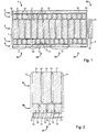
- Fig. 1 depicts a photovoltaic module 1.
- the module 1 comprises different homogeneous zones 2-6.
- Zones 2-6 substantially extend parallel to each other in one longitudinal direction essentially over the whole module length and thus cover most of the module surface. Both ends of each of the zones 2-6 are connected to busbars 7, 8, corresponding to a cathode 7 and an anode 8 for a total collection of the photocurrent generated by module 1.
- Zones 2-6 comprise a module bypass zone 2, a first photovoltaic cell zone 3, a second photovoltaic cell zone 4, a submodule bypass zone 5, a third photovoltaic cell zone 6, and a blocking diode zone 20.
- the first photovoltaic cell zone 3 comprises fifteen photovoltaic cells 9 interconnected in series via contacts 10 to a submodule 3 and constitutes a secondary power-generating submodule 3.
- the second photovoltaic cell zone 4 comprises twelve photovoltaic cells 11 which are series-connected via contacts 12 and 13 and constitutes a main power-generating submodule 4.
- the third photovoltaic cell zone 6 comprises sixteen photovoltaic cells 14 which are series-connected via contacts 15 and 13 and constitutes a second secondary power-generating submodule 6.
- the main power-generating submodule 4 is disposed at the center of the module 1 and its photovoltaic cells 11 are approximately six times larger compared to the substantially equally sized photovoltaic cells 9, 14, of the secondary power-generating submodule 3 and of the second secondary power-generating submodule 6 respectively.
- the total area covered by the main power-generating submodule 4 roughly corresponds to the summed up area covered by the other zones 2, 3, 5, 6.
- the submodule bypass zone 5 is disposed below the third photovoltaic cell zone 6 and comprises four bypass diodes 16 that are interconnected in series via contacts 17 and 13.
- the module bypass zone 2 comprises one bypass diode 18 extending essentially over the whole module length and being interconnected with cathode 7 and anode 8 via contacts 19.
- the widths of bypass diode 18 from module bypass zone 2 and bypass diodes 16 from submodule bypass zone 5 are essentially the same and roughly correspond to the side length of the essentially square shaped photovoltaic cells 9, 14, of the secondary power-generating submodules 3, 6.
- the end side at anode 8 is formed by a blocking diode zone 7, comprising a blocking diode 21 in which the anode busbar 8 is included and that is interconnected in series with all zones 2, 3, 4, 5, 6 via a contact 22.
- each parallel submodule consists of three series-connected photovoltaic cells 11 from main power-generating submodule 4, four series-connected photovoltaic cells 14 from the second secondary power-generating submodule 6, and one intermediate bypass-diode 16 from submodule bypass zone 5, that are interconnected in parallel via contacts 13 at the ends of each parallel submodule 23, 24, 25, 26.
- Each of the described zones 2, 3, 4, 5, 6 comprises at least one area section fabricated by application of a patterning scheme on a film layer 90 as depicted in Fig. 5 and further detailed below.
- Each of the described photovoltaic cells 9, 11, 14 and bypass diodes 16, 18 comprises one of these area sections which subsequently are - for simplicity reasons - denoted with the corresponding reference numeral 9, 11, 14, 16, 18.
- All area sections 9, 11, 14, 16, 18 in the same zone 2, 3, 4, 5, 6 substantially exhibit the same compositional and/or structural properties of film layer 90.
- area sections 9, 11, 14, 16, 18 in at least two different zones 2, 3, 4, 5, 6 exhibit different compositional and/or structural properties of film layer 90.
- area sections 11 differ in their film layer properties from area sections 9, 14, 16, 18 and area sections 9, 14 also differ in their film layer properties from area sections 16, 18.
- Fig. 2 depicts one parallel submodule 24.
- the single portions of zones 4 and 6 in each parallel submodule 23, 24, 25, 26 correspond to lowest-level submodules 34, 36.
- the lowest-level submodules 34, 36 and a submodule bypass diode 16 are connected in parallel.
- zones 2, 3, 6 correspond to different rows of photoactive area sections 9, 11, 14, wherein said rows 2, 3, 5 are disposed substantially parallel to each other.
- zones 2, 5 correspond to rows consisting of one or more bypass diodes 17, 18 that are also arranged essentially in parallel with respect to rows 2, 3, 5.
- All area sections of photovoltaic cells 9, 11, 14 as well as the diodes 16, 18, 21 are formed from the same film layer 90 by application of the patterning scheme, i.e. their respective surface area corresponds to different area sections of the same film layer 90.
- Contacts 10, 12, 15, 17 are formed from a different layer that is subsequently deposited on said film layer and by applying a different patterning scheme.
- the different sizing of said area sections of photovoltaic cells 9, 11, 14 allows matching of voltages at their maximum power point (MPP) despite variations of film layer properties in the upright direction.
- MPP maximum power point
- the different sizing of area sections with respect to film layer variations is further exploited for the formation of components with different properties, in particular which do not serve as photovoltaic generators, e.g., diodes 16, 18, 21.
- the secondary submodules 3, 6 are voltage matched to each other and to the main power-generating submodule 4.
- the lowest-level submodules 34, 36 are also voltage matched with respect to each other and with lowest-level submodules 34, 36 of other parallel submodules 23, 24, 25, 26.
- a module would typically contain more elements than shown in Fig. 1 , thereby easing voltage matching between individual submodules.
- the cell proportions could be different.
- both lowest-level submodules exhibit the same submodule voltage when all cells are operated at their MPP, i.e., they are voltage matched, which is ideal for the parallel connection. In this way, current generated by cells in zone 6 can be used to contribute to the total module current.
- the power output of a module is maximized, when the module contains submodules with different material properties connected in parallel.
- a submodule 36 with a lower (predicted) independent power output at its MPP is patterned to produce a different number of series connected cells so that its submodule MPP voltage at least equals the MPP voltage of the submodule 34 with superior power production properties, wherein within this restriction, the MPP voltage of secondary submodule 36 remains as closely matched to the MPP voltage of the main power producing submodule 34, as can be achieved by the described method of subdividing submodule 3, or 36, into the adequate number of series connected cells.
- the resulting difference in MPP voltage between main and secondary submodules will therefore be strongly reduced.
- the main submodule 4 can work at or close to its MPP at all times, while the secondary submodule 36 or submodules 3 and 6 remain close to their MPP and thus contribute to overall power generation even if they are made out of material yielding inferior cells.
- the MPP voltage of the most power-generating submodule 4 is chosen and subsequently serves as reference for the MPP voltage determination of the remaining submodules 3, 6, as described above. Patterning of modules that does not consider this, for example in modules with cells spanning over inhomogeneities, suffer extensively from power loss by current flowing back through the forward-biased junctions of the zones with lowest open-circuit voltage.
- Fig. 3 depicts a representation of a photovoltaic cell 40 in a circuit diagram.
- the photovoltaic cell 40 consists of a current generator 41 and a diode 42 connected anti-parallel, i.e., the diode's forward current flows in a direction opposite to the direction of the generator's current flow.
- a voltage exceeding the diode's 42 threshold voltage exists over the photovoltaic cell terminals 43, a significant part or all of the current generated by the current generator 41 can flow back through diode 42 and hence through the photovoltaic cell.
- a simple equivalent circuit of a non-ideal cell includes a shunting or parallel resistance 44 and a series resistance 45 to more adequately describe a real photovoltaic cell.
- An optional bypass diode 46 may also be integrated in the cell design.
- Fig. 4 is a circuit schematic diagram of a photovoltaic module 50 equivalent to module 1 depicted in Fig. 1 .
- elements in brackets 51, 52, 53 are understood as being series-connected with as many repetitions as the respective bracket index n, m, p, which represents a positive integer, indicates.
- the represented module 50 consists of a series connection of p submodules 53, a module bypass diode 54, and a blocking diode 55 to prevent any current from flowing back through the module.
- Each of the p submodules 53 is a parallel connection of two lower-level submodules 51, 52, and of a submodule bypass diode 56.
- One of the lower-level submodules is made of a series connection of n cells represented as ideal photovoltaic cells with a current generator 57 and a diode 58 for simplicity, each connected in parallel with an optional bypass diode 59 as in Fig. 2 .
- the other of the lower-level submodules 52 is made of a series connection of m cells with a current generator 60 and a diode 61, each connected in parallel with an optional bypass diode 62 as well.
- n would be equal to zero.
- the above-described patterning scheme suggests that the optoelectronic properties of different zones 2, 3, 4, 5, 6 of the deposited films are taken into account and patterning is performed accordingly, such that the voltage over the n cells of one submodule 51 equals the voltage over the m cells of the other submodule 52, thereby advantageously enabling all p submodules 53 to generate more electrical power as compared to common patterning methods.
- m and n would stand for larger numbers than 3 or 4, e.g. of the order of 10-50.
- the configuration shown in Fig. 4 is one example of countless combinations of submodules, cells, and/or bypass diodes, where every submodule again may consist of one or several submodules, cells, and/or bypass diodes. The most suitable combination depends on the optoelectronic properties of the material to be patterned and the geometry of the module.
- a partially shaded or damaged module is protected from significant and permanent or further damage while its power output is increased.
- the module is assumed to contain a zone (PV-Zener zone) where photovoltaic cells with low reverse-breakdown voltage can be created.
- photovoltaic cells correspond to a photovoltaic Zener diode, i.e., a Zener diode showing photovoltaic activity.
- Zener diode i.e., a Zener diode showing photovoltaic activity.
- Patterning is performed such that in a zone, one or several submodules are generated by parallel connection with main power-generating submodules. In this way, such a submodule serves as a reverse bias protection to the module section it spans. At the same time, said submodule still yields power under illumination.
- bypass diodes that are either permanently shaded from irradiation, or do not generate a photocurrent when illuminated, are formed in a zone where preferably the threshold voltage is less than the threshold voltage of the zones containing the main cells.
- a low threshold voltage is desirable because the electric losses in case of an active bypass are proportional to the voltage drop it creates.
- Shading of photoactive diodes is favorable because photocurrent generated in an anti-parallel connected element is opposed to the current produced in the cells of the module, thus eliminating part of the net current and power created by the module.
- Fig. 5 schematically illustrates an apparatus 70 for the fabrication of monolithically-integrated photovoltaic modules, such as module 1 depicted in Fig. 1 .
- the apparatus comprises three material sources 71-73, an In/Ga-source 71, a Se-source 72 and a Cu-source 73, which are suited to deposit a film layer consisting of Cu(In,Ga)Se 2 on a deposition area 74.
- the deposition area 74 may consist of a substrate that is continuously moved in a transport direction 75 that is transverse to the respective deposition profiles 76-78 of material sources 71-73.
- transverse direction 79 corresponds to the upright direction of module 1 also depicted in Fig. 1 .
- deposition control means 80 which are schematically illustrated on both sides of source 73 in Fig. 5 .
- Fig. 6 is an area chart that shows the total amount of the different materials 91-93 that are deposited on deposition area 74 in said transverse direction 79 after passing the three sources 71-73, respectively, such that a film layer 90 is formed on deposition area 74.
- Fig. 7 is an area chart that shows the corresponding material percentage composition of film layer 90 in said transverse direction 79.
- deposition control means 80 in the form of screens, shields, or shadow masks may be employed to alter the effective deposition profiles of certain sources, as illustrated in Fig. 5 .
- bypass diode The shading of a bypass diode on the other hand can be achieved as a post cell production step, and using bypass material similar to the cell material may be an adequate solution in this case.
- CIGS copper-indium-gallium-diselenide
- These cells typically consist of a molybdenum back contact, on which the CIGS absorber layer, forming the p-type semiconductor, is deposited.
- the CIGS layer is coated by a CdS buffer layer and one or two undoped or doped ZnO layers as n-type semiconductors and as a transparent conductive window layer, serving as front contact.
- the cells produced by this process show very important dependencies between copper content and photoelectric properties. More specifically, it has been measured that a standard Cu:In:Ga:Se atomic percentage composition of about 22:23:5:50 yields cells with a photovoltaic light to electricity conversion efficiency exceeding 10 percent. These cells typically show a short-circuit current density of about 30 mA/cm 2 and an open-circuit voltage of about 550 mV. Increasing the relative copper content reduces both short circuit current density and open circuit voltage of the cells. It is thus clear that the standard composition could be used for the main power generating elements in a module.
- zones with higher copper content may exist. Since cells in these zones exhibit reduced open-circuit voltage it is preferable to create parallel submodules 2, 3, 4, 5, 6 in these zones to avoid draining the voltage away from each zone's MPP as described above.
- the photocurrent becomes small or even zero while the open circuit voltage decreases to below 300 mV.
- Such material is well suited for shaded, or if negligible current is generated, unshaded bypass diodes as explained above.
- compositions with increased copper content can show Zener-diode behavior at voltages as low as -500 mV.
- a small additional copper flux towards the centerline of the module in its moving direction may generate a bypass diode zone along this line that does not require shading. Furthermore, since it is in the middle of the module, the bypass diode advantageously provides the least resistive losses when the current has to be collected over the module width to be passed through the diode.
- a copper-rich zone is created near the edges of the module where framing of the module could easily shade the diodes.
- a photovoltaic module optimized for a given application may this be lifetime energy yield, damage tolerance, process yield, manufacturing cost per kWh, manufacturing cost per Watt peak, or further demands.
Description
- The invention relates to a method and apparatus for fabricating monolithically-integrated photovoltaic modules, according to claims 1 and 9. The invention also relates to a photovoltaic module according to claim 10. The method comprises the steps of forming a film layer on a deposition area such that at least a portion of said film layer constitutes a photoactive layer, applying a patterning scheme for dividing said film layer into area sections and providing electrically interconnected components, each comprising at least one of said area sections. The photovoltaic module comprises at least one film layer, said film layer being divided into area sections, and electrically interconnected components, each comprising at least one of said area sections. More particularly, the invention relates to the fabrication of photovoltaic modules with a film layer formed by, but not limited to, an ABC2 material, wherein A represents elements in
group 11 of the periodic table of chemical elements as defined by the International Union of Pure and Applied Chemistry including Cu or Ag, B represents elements ingroup 13 of the periodic table including In, Ga, or Al, and C represents elements ingroup 16 of the periodic table including S, Se, or Te. - Thin-film photovoltaic cells such as Cu(In,Ga)Se2- (CIGS-) or CdTe-based photovoltaic cells show a high potential for cheaper solar electricity, lower energy payback time, and improved life cycle impact as compared to traditional wafer-based silicon photovoltaic cells. These advantages originate mostly from three factors: First, thin-film absorbers can absorb solar radiation within very thin layers of the order of micrometers. Second, thin-film photovoltaic modules can be produced in-line and in large sizes with a high degree of automation and thus little labor cost. Third, thin-film photovoltaic cells can be monolithically integrated to photovoltaic modules.
- Such a photovoltaic module essentially consists of an array of interconnected photovoltaic cells and optional additional devices such as bypass diodes, directly or indirectly connected to current collectors (busbars) and on, or in between, supporting structures for protective and/or mechanical reasons. The term "monolithical integration" means that several photovoltaic cells on the same substrate can be interconnected during manufacturing to form a module on that substrate, whereas non-monolithically-integrated modules (such as wafer-based modules) consist of individual photovoltaic cells requiring manual interconnection after cell manufacturing.
- For the sake of monolithical integration, some or all of the photovoltaic module films need to be patterned in one or several processing steps at one or different stages of the manufacturing process, either during or after the deposition of individual layers or during or after deposition of groups of layers,see for example M. Powalla and D. Bonnet, Advances in OptoElectronics, vol. 2007, Article ID 97545, 2007. Patterning is usually achieved by applying a predefined patterning scheme in order to divide the photoactive film layer and/or auxiliary layers, e.g. back contact, absorber, buffer, window, and front contact layers, in several area sections for defining location, size, and shape of module elements, in particular photovoltaic cells. Patterning is further performed such that at least two interconnects can be formed to each module element - typically to each element's plus and minus pole, respectively - such that the element is connected either in parallel or in series to other, typically adjacent, module elements or to the busbar. Common patterning techniques are scribing methods such as mechanical or laser scribing of one or several layers at a time, but also shadowing, lithography, or other methods are used, as described for example in
WO 03/061013 A1 - Each photovoltaic cell has a maximum power point (MPP), which denotes the condition of a cell, under which it delivers the highest amount of electrical power under given illumination conditions. When photovoltaic cells consist of material with inhomogeneous optoelectronic properties, the following problems may arise: A large photovoltaic cell can be thought of as a submodule consisting of the parallel connection of smaller cells which together cover the same area as the large cell. As soon as the voltage across this submodule exceeds the diode threshold voltage of one of the smaller cells, the current produced by the other cells starts to flow back through that cell with the lowest diode threshold voltage. Hence, cells with a high MPP voltage cannot be operated at that voltage without losing too much current due to current reversal. In other words, the MPP voltage of the submodule is dragged towards the MPP voltage of the cell with the lowest diode threshold voltage. If the differences in MPP voltage between the small cells are large, many cells are operated below their MPP, thereby reducing submodule efficiency. In the extreme case, owing to the presence of one weak cell, all other cells connected in parallel may operate at non-optimum efficiency in order to operate the submodule at its MPP. Therefore, it is highly desirable that any photovoltaic cell possess homogeneous optoelectronic properties across its area in order to deliver maximum electrical power.
- Since a real cell is typically not totally homogeneous in its optoelectronic properties and also shading of one or more cells may occur, the current difference will flow through the weakest spot of the weakest cell or shaded cell, where the local reverse-breakdown voltage is lowest. In that weak spot, a very large local current density may occur and induce permanent cell damage due to overheating. In order to avoid a resulting degradation of the whole photoactive area of the photovoltaic module, a reverse bias protection can be employed, e.g. in the form of a bypass diode: When a negative bias voltage builds up across a photovoltaic cell and the threshold voltage of the bypass diode is exceeded, then reverse current can flow through the bypass diode instead of through the weak spot of the weakest or shaded cell, provided that the threshold voltage of the bypass diode is lower than the reverse-breakdown voltage of the photovoltaic cell's weak spot.
- Bypass diodes can be incorporated into monolithically-integrated thin-film modules by connecting photovoltaic cells anti-parallel, i.e. with their polarities reversed. The diodes can be formed over single cells, lower- and higher-level submodules consisting of several cells, and also over the whole module, to another cell or to a string of other cells. These diodes traditionally have been discrete components attached to the photovoltaic module by soldering or similar techniques. Another technique for creating integrated diodes includes adding additional layers non-monolithically onto the bottom or surface of the cell, as described for example in
U.S. patent no. US 6,635,507 . A diode can also be formed by monolithic integration into the module as described in patent no.US 6,690,041 . These integration techniques of a diode generally require a number of additional processing steps and/or material to be applied on the device. Thus, one of their disadvantages lies in an increase of complexity and costs for device manufacturing. - The electrical performance of each of the described components of a photovoltaic module, i.e. photovoltaic cells, submodules, bypass diodes, etc., are ordinarily described by one or several characteristic values of their respective current-voltage characteristic curves. For instance, the open-circuit voltage and/or the current/voltage at the maximum power point are often quoted with respect to photovoltaic cell or photovoltaic submodule properties. A diode behavior is generally well described by the value of the threshold voltage. In the special case of a Zener diode, the reverse breakdown voltage is a characteristic value.
-
WO 2008/042682 A2 describes a thin film photovoltaic module, in which an undesired non-uniformity of the film layer shall be compensated. To this end, the module is divided into single photovoltaic cells along the direction, in which the non-uniformity of the film layer occurs. According to another embodiment, such a division can also be carried out within several submodules of the module, wherein corresponding submodules in an area zone of a given film-layer uniformity are series connected to a set of submodules, and these different sets of submodules are mutually connected in parallel. In another embodiment, protect diodes are fabricated on the film layer as a part of the lithographic process during which adjacent photovoltaic cells are connected. The protect diodes are arranged in parallel to the direction, in which the film layer is divided into single photovoltaic cells, such that they are fabricated from the same film layer properties as the photovoltaic cells. This has the disadvantage that deviating film properties, which may be required for a reliable functionality of these additional components, are not inherently accounted for, and additional processing steps may be required to improve their performance. - It is an object of the present invention to avoid at least one of the above mentioned disadvantages and to provide a method and/or an apparatus which allows the fabrication of monolithically-integrated photovoltaic modules comprising interconnected photovoltaic cells with requirement-matched photovoltaic properties, in particular such that deviations of the voltage and/or current at the maximum power point of said photovoltaic cells are substantially reduced and/or the power output of the total available photoactive area is optimized. It is another object of the invention to provide a method and/or an apparatus for monolithically integrating further components, such as bypass diodes and/or resistances, in a photovoltaic module, wherein the fabrication process and/or the structural composition of such a module is simplified and suitable film properties for the further components are accounted for. It is a further object of the invention to allow the fabrication of a photovoltaic module at reduced production costs and/or to provide a photovoltaic module exhibiting at least one of the above-mentioned properties.
- At least one of the above objects is achieved with a method comprising the features of patent claim 1, as well as an apparatus comprising the features of patent claim 9, as well as a photovoltaic module comprising the features of patent claim 10. Advantageous embodiments of the invention are defined in the dependent claims.
- In a method for fabricating monolithically-integrated photovoltaic modules, the invention suggests that at least one compositional and/or structural property, in particular material percentage composition and/or thickness, of said film layer is varied over said deposition area and said patterning scheme is applied in such a way that at least one of said film layer variations in at least one of said area sections is reduced with respect to the corresponding film layer variation over said deposition area. In this way, at least two of said area sections are provided with substantially differing compositional and/or structural properties such that at least two of said components exhibit substantially differing current-voltage characteristics. Furthermore, said at least two components are interconnected in parallel for exploiting at least one advantage of said differing current-voltage characteristics:
One of the advantages may arise from the possibility of voltage matching of at least two components consisting of single photovoltaic cells or submodules, each comprising several photovoltaic cells in a series connection, wherein said different current-voltage characteristics may comprise a different current value at a substantially equal voltage value at the maximum power point and/or a different open circuit voltage of these components. Another advantage may include the possibility of a simplified monolithic integration process of additional components, in particular bypass diodes, resistors and/or Zener diodes, wherein said different current-voltage characteristics may comprise a different diode threshold voltage and/or a different reverse breakdown voltage. - Advantageously, said current-voltage characteristics of at least two of said components may differ by a factor of at least 2 percent, more preferred by a factor of at least 5 percent, and most preferred by a factor of at least 10 percent.
- Said variations of at least one compositional and/or structural property of said film layer may occur or be imposed over said deposition area. In particular, said compositional and/or structural and/or voltage properties may comprise the material percentage composition and/or the thickness of said film layer. In this way, film patterning processes may be correlated with spatial variations of film properties such as electronic, compositional, optoelectronic, or structural properties.
- According to one embodiment, this correlation of patterning with spatial variations of film properties may be exploited to tailor photovoltaic cell patterns and geometries such that each individual photovoltaic cell exhibits comparable photovoltaic properties and consequently good current and voltage matching can be achieved. In particular, the lifetime electricity generation of the module may be maximized and/or the temporal power output profile of the module may be optimized, while at the same time conditions and restrictions on thin-film deposition processes can be relaxed and/or material utilization yield during the deposition process may be improved. According to another embodiment, said correlation of patterning with spatial film variations may be exploited for creating further tailored units such as bypass diodes, resistances, or conductors. The aforementioned benefits may therefore advantageously contribute to a decrease of the cost of solar electricity generation. Preferably, such a tailoring of photovoltaic cell patterns may be achieved by applying said patterning scheme in such a way that at least one geometrical property, in particular the size and/or shape and/or orientation and/or areal number, of said area sections is varied in dependence of at least one of said film layer variations. In this way, single photovoltaic cells and/or submodules, each comprising several photovoltaic cells in a series connection, may be provided with a substantially equal voltage value at their maximum power point.
- Advantageously, said patterning scheme may be applied in such a way as to subdivide said deposition area into area zones with different compositional and/or structural properties of said film layer, at least one of said area zones comprising area sections with essentially the same compositional and/or structural properties of said film layer. At least one of said components in at least one area zone may be provided by a submodule, each comprising several single photovoltaic cells in a series connection.
- In order to allow matching of said patterning scheme to specific requirements, said method may comprise the further steps of determining at least one of said film layer variations and adjusting said patterning scheme in dependence thereof. In particular, this step may comprise measuring of local properties of said film layer by means of non-destructive tests. Additionally or alternatively, said determination of at least one of said film layer variations may be based on empirical values and/or based on theoretical calculations and/or performed by testing of prior batches and/or by testing of periodic zones of said film layer, in particular of sacrificial zones, etc.
- To achieve a more uniform distribution of said compositional and/or structural and/or voltage property on said area sections of said film layer, at least one of said area sections with a larger size may be arranged in a region where said film layer variations are small as compared to at least one of said area sections with a smaller size that is arranged in a region where the corresponding film layer variations are larger.
- Advantageously, in particular for creating the desired photovoltaic properties on said area sections, said patterning scheme may be applied such that the local single photovoltaic cell current-voltage characteristics in at least one submodule is reduced with respect to local photovoltaic cell current-voltage characteristics of another submodule by a factor of at least 2 percent, more preferred by a factor of at least 5 percent and most preferred by a factor of at least 10 percent.
- Advantageously, said application of said patterning scheme may subdivide the photovoltaic module into zones of improved homogeneity of photovoltaic properties such that particularly the voltage at the maximum power point (MPP) in the predominant zone is increased by at least the open circuit voltage of a photovoltaic cell thus created in the zone of lower open circuit voltage properties. Thereby, the homogeneity improvement permits operating the entire zone closer to the local MPP conditions and thus improves efficiency.
- Preferably, said forming of a film layer comprises the steps of evaporating and depositing material on said deposition area from at least one material source, wherein said deposition area is moved with respect to said material source and said varying of at least one compositional and/or structural property of said film layer is carried out transverse to the respective moving direction. Thus, a continuous manufacturing process may be provided by varying said compositional and/or structural property in at least one or two dimensions and by moving said deposition area in a different direction. Such a method may be integrated in a so called roll-to-roll manufacturing technology for allowing continuous deposition of said film layer at high speeds under rolling of said deposition area. For allowing said rolling, said deposition area may be constituted by a plastic substrate.
- In order to account for said transverse variation of said film layer properties, at least two, more preferred at least three, of said area sections may be disposed in a transverse direction with respect to said moving direction. In order to account for an inhomogeneous deposition rate along said transverse direction, in particular for a smaller variation of deposed material at a center portion, area sections with a larger size may be provided at a center portion of said deposition area with respect to said transverse direction as compared to area sections located at a side portion. According to a specific embodiment, said area sections at said center portion may cover at least two times, more preferred at least three times, more space in that transverse direction as compared to said area sections at said side portion.
- Preferably, said forming of a film layer comprises evaporating and depositing materials on said deposition area from separated material sources, wherein the deposition rate of at least one of said sources is varied over said deposition area such that said varying of compositional properties comprises varying of a percentage composition and/or an absolute quantity of at least one of said deposited materials. In this way, a large variety of possible film layer variations may be achievable, since each source may be manipulated individually and also the relative positioning of the sources may be available as an adjustable parameter.
- Said at least one source may be a point source or a linear source, wherein also sources of any other shape or nature are conceivable. In particular, said film variations may be produced by an inhomogeneous deposition profile of said source with respect to said deposition area, which results in variations of the deposition rate on said deposition area. More preferred, the local deposition rate on said deposition area may vary with distance and angle from the part of said source or sources at which material is leaving the source or sources. In particular, said local deposition rates may vary from said source or sources by a Lambert-cosine law or with a similar behavior. Thus in an advantageous embodiment of the method, deposition-source profiles may be adapted and correlated with suitable cell structuring patterns, such as to improve the optoelectronic properties of photovoltaic cells, bypass diodes, resistances, Zener diodes or conductors.
- Moreover, means to control deposition, in particular shielding means and/or masking means and/or material guiding means, are applied on or in the vicinity of said material source or sources to control at least one of said film layer variations. Thus, adequate control of said deposition rate combined with appropriate application of said patterning scheme may be used to optimize the output power of said module, in particular with respect to full illumination conditions and/or lifetime performance. Alternatively or additionally, the useful deposition width on said deposition area may be optimized thereby. Alternatively or additionally, optoelectronic properties on at least one specific position of said film layer may be altered to provide additional components such as bypass-diodes and/or resistances and/or Zener diodes.
- More generally, at least one of said compositional and/or structural properties of said film layer may be varied to provide at least one bypass-diode and/or resistance and/or Zener diode comprising at least a portion of said film layer on at least one of said area sections after application of said patterning scheme. In particular, said film layer may be altered on one or more regions such that degraded photovoltaic conversion properties are generated in these regions in which said additional components may be provided. For instance, at least one of said properties in at least one of said area sections may be altered such that a lower or a comparatively negligible photocurrent may be generated in this area section, or substantially no photocurrent at all. For instance, said diodes may be placed in a zone where the material composition deposited on said deposition area in essence does not generate a photocurrent. A resulting photovoltaic module may for example comprise several series-connected submodules, which in turn may consist of one or several parallel strings of series connected cells. Different strings may comprise different numbers of cells with individually designed sizes and/or shapes, and some or all of these strings may have properties resulting in reverse bias protection and bypass paths. Preferably, at least one diode is connected so as to block reverse current flow through the module, thereby providing a blocking diode . Preferably, said diodes are placed in zones in which said property variations of said film layer allow a small threshold voltage of said diodes.
- Applying said patterning scheme may enable the production of varieties of submodules that may include said diodes. Said diodes may be formed in such a way that they are connected anti-parallel to parts of the module and/or submodule for reverse bypass protection. The bypass protection may be advantageous when at least one parallel submodule produces less energy than another submodule in the parallel assembly.
- Said patterning scheme may therefore be used to produce submodules of matched voltage at MPP. Said submodules may contain a variety and a combination of series-connected cells, tandem cells, and/or multijunction cells. Matched MPP voltage may be advantageous when connecting submodules in parallel. When differing submodules are connected in parallel, the most powerful submodule of the parallel submodule circuit may be used as a guideline to form less powerful submodules whose MPP voltage is equal to or slightly greater than that of the most powerful submodule. The MPP voltage excess of the less powerful submodules as compared to the most powerful submodule may be capped by the open circuit voltage of one of its series-connected cells.
- Furthermore, said patterning scheme may be used to form one or several current producing submodules that exhibit a Zener-barrier reverse breakdown property or similar behavior, thereby avoiding reverse breakdown damage to the module.
- According to a specific embodiment of the method, simple deposition sources with a low degree of sophistication may be used to deposit thin-film material onto wide substrates. Resulting spatial variations of film properties may then be tolerated in that they do not give rise to module performance losses as compared to prior art devices.
- The method is particularly suited for a film layer that is formed by, but not limited to, an ABC2 material, wherein A represents Cu or Ag, B represents
group 13 materials of the periodic table of elements as defined by the International Union of Pure and Applied Chemistry, including in particular In, Ga, or Al, and C represents S, Se, or Te. For instance, said film layer may be formed of Cu(In,Ga)Se2 which is particularly suited for the implementation of this method. However, also other materials are conceivable such as CdTe-layers. - For a film layer formed by said ABC2 material the deposition rate and distribution may be varied spatially so that in said area sections the material thickness deviates in at least two of said area sections by at least 5 percent and/or at most 30 percent, preferably at most 20 percent. Additionally or alternatively, the compositional ratio of Cu to
group 13 material of the periodic table of chemical elements as defined by the International Union of Pure and Applied Chemistry may range from 0.6 to 0.9. - Said application of a patterning scheme may be achieved by mechanical scribing or laser scribing. Application of any other adequate means is also conceivable. Said application of a patterning scheme may be executed between two or several successive production steps, in particular between successive deposition of various layers. Said application of a patterning scheme may also be executed after deposition of all layers. Alternatively, a formation of interconnections and/or insulation may be achieved by deposition of various materials, such as contact grids and/or polymers, wherein further materials are also conceivable. In particular, said patterning may result in interconnected cells, submodules with several cells, and/or diodes.
- According to a further aspect of the invention, an apparatus for the fabrication of monolithically-integrated photovoltaic modules is provided, said apparatus being defined in claim 10 and comprising at least one evaporation source that is adapted to deposit a film layer with at least one compositional and/or structural property varying over said deposition area and a patterning means that is adapted to divide said film layer into at least two of said area sections with substantially differing compositional and/or structural properties, such that at least two of said components exhibit substantially differing current-voltage characteristics. Furthermore, said apparatus is adapted to interconnect said at least two components in parallel.
- Advantageously, said apparatus may in particular be adapted for a variation of the material percentage composition and/or the thickness of said film layer. According to a specific embodiment, said sources may comprise at least one of Cu, Ag, In, Ga, Al, S, Se and Te sources. According to the invention, said apparatus further comprises means to control deposition, in particular shielding means and/or masking means and/or material guiding means, for at least one of said material sources in order to control at least one of said film layer variations.
- Preferably, said apparatus is in particular suited for execution of the above described method and may further comprise at least one additional appropriate means known in the art per se for conducting various steps of this method.
- According to another aspect of the invention, a photovoltaic module as defined in claim 10 is provided comprising at least one film layer divided into electrically interconnected area sections, wherein at least a portion of said film layer constitutes a photoactive layer. The module further comprises electrically interconnected components each comprising at least one of said area sections. At least two of said area sections of said film layer are provided with substantially differing compositional and/or structural properties, such that at least two of said components exhibit substantially differing current-voltage characteristics. Said at least two components are interconnected in parallel for exploiting at least one of the advantages arising from said differing current-voltage characteristics. Thus, photovoltaic properties may be improved in such a module, in particular according to the above described manner. Furthermore, an implementation of additional components, such as diodes and/or resistances may be provided, in particular according to the above described manner. Thus, a bypass diode and/or resistance comprising at least a portion of said film layer may be provided by at least one of said components. In particular, said area sections may vary in their material percentage composition and/or thickness of said film layer.
- Advantageously, said film layer may be divided into area zones with different compositional and/or structural properties of said film layer, at least one of said area zones comprising area sections with essentially the same compositional and/or structural properties of said film layer, and at least one of said components is provided by a submodule comprising a series connection of photovoltaic cells each comprising one of said area sections in said at least one area zone. Furthermore, at least two of said area sections may be provided with a different geometrical property comprising at least one of size, shape, orientation and areal number.
- Preferably, such a photovoltaic module may exhibit advantageous performance properties according to which the voltage and/or current at the maximum power point (MPP) of said at least two photovoltaic cells and/or submodules may differ. Alternatively or additionally, this may be achieved if at least one of said area sections with a smaller areal size is provided more closely to a side portion of said photoactive layer as compared to at least one of said area sections with a larger areal size. Thereby, several or each of said area sections may constitute a photoactive device, in particular a photovoltaic cell or above mentioned submodule.
- Advantageously, repeating arrangements of at least two of said area sections may be provided, in particular in the form of above mentioned submodules, said repeating arrangements being subsequently disposed in at least one direction of said film layer. In such a way, various zones with substantially identical properties may be provided in a continuous fabrication process. Advantageously, all photoactive area sections enclosed in one of said repeating arrangements may be bypassed by at least one of said bypass diodes and/or resistances and/or Zener diodes. This allows comparatively stable operation of the module even if portions of its surface are shaded and/or one or several single cells exhibit poor photovoltaic performance properties.
- Advantageously, at least two rows of area sections may be disposed substantially parallel to each other on said film layer, wherein said differing compositional and/or structural properties of said film layer are provided for at least two of said area sections in different rows. As such, several or each of said area sections may constitute a photoactive device, in particular a photovoltaic cell or submodule. Said area sections may be in series connection along said rows and/or in parallel connection in between said rows. In this way, matching of the voltages at the MPP of said area sections of each row may be achieved.
- Advantageously, said area sections in different rows may differ in their respective length in the direction of said variation of said compositional and/or structural property of said film layer. Such an arrangement may be particularly suited for voltage matching between different rows. Furthermore, said rows with shorter area sections in the direction of said variation of said compositional and/or structural property of said film layer may contain a larger number of area sections in order to achieve said voltage matching of said rows.
- Advantageously, repeating arrangements of said submodules may be disposed along the length of said film so as to constitute said module, said repeating arrangement of submodules being bypassed by at least one of said bypass diodes.
- The invention is described in more detail in the following description of preferred exemplary embodiments with reference to the accompanying drawings.
-
- Fig. 1
- is a schematic view of a photovoltaic module comprising several submodules;
- Fig. 2
- is a schematic view of a submodule of the photovoltaic module shown in
Fig. 1 ; - Fig. 3
- is a circuit diagram representing an ideal and a real photovoltaic cell;
- Fig. 4
- is a circuit diagram representing a photovoltaic module comprising several submodules;
- Fig. 5
- is a schematic view of an apparatus for the fabrication of monolithically-integrated photovoltaic modules;
- Fig. 6
- is a diagram representing the amount of material deposited on a deposition area by means of the apparatus shown in
Fig. 5 ; and - Fig. 7
- is a diagram representing the corresponding material percentage composition of the deposition profile according to
Fig. 6 . - Subsequently, a manufacturing method and resulting monolithically integrated thin-film photovoltaic modules are described, where film patterning processes are correlated with spatial variations of film properties such as electronic, compositional, optoelectronic, or structural properties. As a result, units with homogeneous properties across their area, e.g., photovoltaic cells with homogeneous optoelectronic performance, can be created. Properties may vary from unit to unit, however. In this way, a potentially inhomogeneous large-area film or film stack can be divided into comparatively homogeneous zones. This, on the one hand, allows to improve the electricity generation performance of a module relative to the performance of a conventionally-scribed module exhibiting some inhomogeneous film properties, while on the other hand it also allows to relax the demands on the deposition sources. The latter is because inhomogeneous material deposition profiles no longer lead to degraded module performance. This is advantageous in that one may then employ less sophisticated and more robust and less expensive deposition sources while improving material utilization yield.
- The determination of local film properties may be based on theoretical considerations originating from knowledge about the source properties, on analysis of experimental data gathered from prior runs, or on methods that allow the local analysis of materials properties immediately before calculating and applying the optimal patterning scheme.
- In one embodiment of the invention, one or several films on a substrate are patterned such that any so-defined lowest-level submodule contains current-matched photovoltaic cells. Furthermore, such submodules connected in series and/or parallel can also be designed to be current and/or voltage matched, such that every photovoltaic cell can be operated at its maximum power point, or at least such that no photovoltaic cell under operation delivers less than 90 percent of the power it could deliver at its maximum power point (MPP).
-
Fig. 1 depicts a photovoltaic module 1. The module 1 comprises different homogeneous zones 2-6. Zones 2-6 substantially extend parallel to each other in one longitudinal direction essentially over the whole module length and thus cover most of the module surface. Both ends of each of the zones 2-6 are connected tobusbars cathode 7 and ananode 8 for a total collection of the photocurrent generated by module 1. Zones 2-6 comprise a module bypass zone 2, a first photovoltaic cell zone 3, a second photovoltaic cell zone 4, a submodule bypass zone 5, a thirdphotovoltaic cell zone 6, and a blockingdiode zone 20. - In
Fig. 1 , the first photovoltaic cell zone 3 comprises fifteen photovoltaic cells 9 interconnected in series via contacts 10 to a submodule 3 and constitutes a secondary power-generating submodule 3. The second photovoltaic cell zone 4 comprises twelvephotovoltaic cells 11 which are series-connected viacontacts photovoltaic cell zone 6 comprises sixteenphotovoltaic cells 14 which are series-connected viacontacts submodule 6. The main power-generating submodule 4 is disposed at the center of the module 1 and itsphotovoltaic cells 11 are approximately six times larger compared to the substantially equally sizedphotovoltaic cells 9, 14, of the secondary power-generating submodule 3 and of the second secondary power-generatingsubmodule 6 respectively. Thus, the total area covered by the main power-generating submodule 4 roughly corresponds to the summed up area covered by theother zones 2, 3, 5, 6. - The submodule bypass zone 5 is disposed below the third
photovoltaic cell zone 6 and comprises fourbypass diodes 16 that are interconnected in series viacontacts - The module bypass zone 2 comprises one bypass diode 18 extending essentially over the whole module length and being interconnected with
cathode 7 andanode 8 viacontacts 19. The widths of bypass diode 18 from module bypass zone 2 andbypass diodes 16 from submodule bypass zone 5 are essentially the same and roughly correspond to the side length of the essentially square shapedphotovoltaic cells 9, 14, of the secondary power-generatingsubmodules 3, 6. The end side atanode 8 is formed by a blockingdiode zone 7, comprising a blockingdiode 21 in which theanode busbar 8 is included and that is interconnected in series with allzones 2, 3, 4, 5, 6 via acontact 22. - The positions of the three
contacts 13 define four parallelupright zones parallel submodules parallel submodules photovoltaic cells 11 from main power-generating submodule 4, four series-connectedphotovoltaic cells 14 from the second secondary power-generatingsubmodule 6, and one intermediate bypass-diode 16 from submodule bypass zone 5, that are interconnected in parallel viacontacts 13 at the ends of eachparallel submodule - Each of the described
zones 2, 3, 4, 5, 6 comprises at least one area section fabricated by application of a patterning scheme on afilm layer 90 as depicted inFig. 5 and further detailed below. Each of the describedphotovoltaic cells bypass diodes 16, 18 comprises one of these area sections which subsequently are - for simplicity reasons - denoted with thecorresponding reference numeral area sections same zone 2, 3, 4, 5, 6 substantially exhibit the same compositional and/or structural properties offilm layer 90. However,area sections different zones 2, 3, 4, 5, 6 exhibit different compositional and/or structural properties offilm layer 90. For instance,area sections 11 differ in their film layer properties fromarea sections area sections 9, 14 also differ in their film layer properties fromarea sections 16, 18. -
Fig. 2 depicts oneparallel submodule 24. The single portions ofzones 4 and 6 in eachparallel submodule level submodules level submodules submodule bypass diode 16 are connected in parallel. - Accordingly, the
zones 2, 3, 6 correspond to different rows ofphotoactive area sections more bypass diodes 17, 18 that are also arranged essentially in parallel with respect to rows 2, 3, 5. All area sections ofphotovoltaic cells diodes same film layer 90 by application of the patterning scheme, i.e. their respective surface area corresponds to different area sections of thesame film layer 90.Contacts photovoltaic cells diodes - The
secondary submodules 3, 6 are voltage matched to each other and to the main power-generating submodule 4. The lowest-level submodules level submodules parallel submodules Fig. 1 , thereby easing voltage matching between individual submodules. Furthermore, the cell proportions could be different. - It is assumed in this example depicted in
Fig. 2 that the material properties ofzone 6 are such that the cells in this zone have an MPP voltage that is about 75 percent lower than the MPP voltage of the cells in zone 4. Hence, both lowest-level submodules exhibit the same submodule voltage when all cells are operated at their MPP, i.e., they are voltage matched, which is ideal for the parallel connection. In this way, current generated by cells inzone 6 can be used to contribute to the total module current. - If current common state-of-the-art patterning methods were applied, this would have the disadvantage of producing larger cells compared to the advantageous structuring of cells into
zones 4 and 6 according to the above described method combined with parallel connection of cells fromzones 4 and 6. A further disadvantage of applying current common state-of-the-art methods would result in the operating voltage being dragged away from the local maximum power points of both zones, therefore effecting a low power output of the module. - In a further embodiment, the power output of a module is maximized, when the module contains submodules with different material properties connected in parallel. For example, with reference to
Fig. 2 , asubmodule 36 with a lower (predicted) independent power output at its MPP is patterned to produce a different number of series connected cells so that its submodule MPP voltage at least equals the MPP voltage of the submodule 34 with superior power production properties, wherein within this restriction, the MPP voltage ofsecondary submodule 36 remains as closely matched to the MPP voltage of the mainpower producing submodule 34, as can be achieved by the described method of subdividingsubmodule 3, or 36, into the adequate number of series connected cells. The resulting difference in MPP voltage between main and secondary submodules will therefore be strongly reduced. - In such a way it is guaranteed that the main submodule 4 can work at or close to its MPP at all times, while the
secondary submodule 36 orsubmodules 3 and 6 remain close to their MPP and thus contribute to overall power generation even if they are made out of material yielding inferior cells. There may be more than twosubmodules submodules 3, 6, as described above. Patterning of modules that does not consider this, for example in modules with cells spanning over inhomogeneities, suffer extensively from power loss by current flowing back through the forward-biased junctions of the zones with lowest open-circuit voltage. -
Fig. 3 depicts a representation of aphotovoltaic cell 40 in a circuit diagram. In an idealized case thephotovoltaic cell 40 consists of acurrent generator 41 and adiode 42 connected anti-parallel, i.e., the diode's forward current flows in a direction opposite to the direction of the generator's current flow. Once a voltage exceeding the diode's 42 threshold voltage exists over thephotovoltaic cell terminals 43, a significant part or all of the current generated by thecurrent generator 41 can flow back throughdiode 42 and hence through the photovoltaic cell. A simple equivalent circuit of a non-ideal cell includes a shunting orparallel resistance 44 and aseries resistance 45 to more adequately describe a real photovoltaic cell. Anoptional bypass diode 46 may also be integrated in the cell design. -
Fig. 4 is a circuit schematic diagram of aphotovoltaic module 50 equivalent to module 1 depicted inFig. 1 . InFig. 4 , elements inbrackets module 50 consists of a series connection ofp submodules 53, amodule bypass diode 54, and a blockingdiode 55 to prevent any current from flowing back through the module. Each of thep submodules 53 is a parallel connection of two lower-level submodules submodule bypass diode 56. One of the lower-level submodules is made of a series connection of n cells represented as ideal photovoltaic cells with acurrent generator 57 and adiode 58 for simplicity, each connected in parallel with anoptional bypass diode 59 as inFig. 2 . The other of the lower-level submodules 52 is made of a series connection of m cells with acurrent generator 60 and adiode 61, each connected in parallel with anoptional bypass diode 62 as well. - Common patterning methods would result in an equal number of cells per submodule m and n, irrespective of the optoelectronic properties of the cells, or there would be no splitting at all into two parallel-connected submodules, i.e., n would be equal to zero. In contrast, the above-described patterning scheme suggests that the optoelectronic properties of
different zones 2, 3, 4, 5, 6 of the deposited films are taken into account and patterning is performed accordingly, such that the voltage over the n cells of onesubmodule 51 equals the voltage over the m cells of theother submodule 52, thereby advantageously enabling allp submodules 53 to generate more electrical power as compared to common patterning methods. - In
Fig. 2 , an example of one of thep submodules 53 according toFig. 4 is illustrated, where n = 3 forsubmodule 34 and m = 4 forsubmodule 36 and an additionalsubmodule bypass diode 17 is added. Typically, m and n would stand for larger numbers than 3 or 4, e.g. of the order of 10-50. The configuration shown inFig. 4 is one example of countless combinations of submodules, cells, and/or bypass diodes, where every submodule again may consist of one or several submodules, cells, and/or bypass diodes. The most suitable combination depends on the optoelectronic properties of the material to be patterned and the geometry of the module. - In a further embodiment, a partially shaded or damaged module is protected from significant and permanent or further damage while its power output is increased. The module is assumed to contain a zone (PV-Zener zone) where photovoltaic cells with low reverse-breakdown voltage can be created. Such photovoltaic cells correspond to a photovoltaic Zener diode, i.e., a Zener diode showing photovoltaic activity. One could also speak of a parallel connection of a Zener diode with a photovoltaic cell, where the reverse breakdown is determined by the Zener diode and the forward current flow threshold is determined by the photovoltaic cell. Patterning is performed such that in a zone, one or several submodules are generated by parallel connection with main power-generating submodules. In this way, such a submodule serves as a reverse bias protection to the module section it spans. At the same time, said submodule still yields power under illumination.
- In yet another embodiment concerning the patterning scheme, thereby protecting partially shaded or damaged modules from permanent or further damage and allowing to increase their power output, bypass diodes that are either permanently shaded from irradiation, or do not generate a photocurrent when illuminated, are formed in a zone where preferably the threshold voltage is less than the threshold voltage of the zones containing the main cells. A low threshold voltage is desirable because the electric losses in case of an active bypass are proportional to the voltage drop it creates. Shading of photoactive diodes is favorable because photocurrent generated in an anti-parallel connected element is opposed to the current produced in the cells of the module, thus eliminating part of the net current and power created by the module. These properties can be achieved by depositing films with inhomogeneous composition in this zone. There are many film compositions that give rise to devices with diode behavior generating only small amounts of or no photocurrent.
-
Fig. 5 schematically illustrates anapparatus 70 for the fabrication of monolithically-integrated photovoltaic modules, such as module 1 depicted inFig. 1 . The apparatus comprises three material sources 71-73, an In/Ga-source 71, a Se-source 72 and a Cu-source 73, which are suited to deposit a film layer consisting of Cu(In,Ga)Se2 on adeposition area 74. Thedeposition area 74 may consist of a substrate that is continuously moved in atransport direction 75 that is transverse to the respective deposition profiles 76-78 of material sources 71-73. As becomes apparent from the particular shape of each of the deposition rate profiles 76-78, the deposition rate of each of the materials is varied in atransverse direction 79 with respect to thetransport direction 75. Therefore,transverse direction 79 corresponds to the upright direction of module 1 also depicted inFig. 1 . The variation of material deposition rate of sources 71-73 can be controlled by applying deposition control means 80, which are schematically illustrated on both sides ofsource 73 inFig. 5 . -
Fig. 6 is an area chart that shows the total amount of the different materials 91-93 that are deposited ondeposition area 74 in saidtransverse direction 79 after passing the three sources 71-73, respectively, such that afilm layer 90 is formed ondeposition area 74. -
Fig. 7 is an area chart that shows the corresponding material percentage composition offilm layer 90 in saidtransverse direction 79. - In order to achieve suitable film properties for bypass diode elements, which are typically very different from the film properties aimed at for photovoltaic cells, it may be necessary to influence a deposition process to induce different material properties in the bypass diode zone 2, 5 of the films. A rapid material deposition transition from cell zones to bypass zones is desirable for exploiting the largest possible part of the module with high quality cells so that a rapid spatial transition to zones with low threshold voltages for the bypass can be achieved. For example, deposition control means 80 in the form of screens, shields, or shadow masks may be employed to alter the effective deposition profiles of certain sources, as illustrated in
Fig. 5 . - The shading of a bypass diode on the other hand can be achieved as a post cell production step, and using bypass material similar to the cell material may be an adequate solution in this case.
- The practicability of the described method and apparatus may be demonstrated on the example of a CIGS (copper-indium-gallium-diselenide) absorber based photovoltaic cell. These cells typically consist of a molybdenum back contact, on which the CIGS absorber layer, forming the p-type semiconductor, is deposited. Typically, the CIGS layer is coated by a CdS buffer layer and one or two undoped or doped ZnO layers as n-type semiconductors and as a transparent conductive window layer, serving as front contact.
- The cells produced by this process show very important dependencies between copper content and photoelectric properties. More specifically, it has been measured that a standard Cu:In:Ga:Se atomic percentage composition of about 22:23:5:50 yields cells with a photovoltaic light to electricity conversion efficiency exceeding 10 percent. These cells typically show a short-circuit current density of about 30 mA/cm2 and an open-circuit voltage of about 550 mV. Increasing the relative copper content reduces both short circuit current density and open circuit voltage of the cells. It is thus clear that the standard composition could be used for the main power generating elements in a module.
- If for example in an evaporation process the homogeneity over the width of the entire substrate is poor, whether originating from deliberate placement of shields, from source design, or from any other intentional or unintentional reason, zones with higher copper content may exist. Since cells in these zones exhibit reduced open-circuit voltage it is preferable to create
parallel submodules 2, 3, 4, 5, 6 in these zones to avoid draining the voltage away from each zone's MPP as described above. By further increasing the copper content above 24% the photocurrent becomes small or even zero while the open circuit voltage decreases to below 300 mV. Such material is well suited for shaded, or if negligible current is generated, unshaded bypass diodes as explained above. Furthermore, compositions with increased copper content can show Zener-diode behavior at voltages as low as -500 mV. - In one exemplary embodiment of the present invention related to CIGS photovoltaic cells, a small additional copper flux towards the centerline of the module in its moving direction may generate a bypass diode zone along this line that does not require shading. Furthermore, since it is in the middle of the module, the bypass diode advantageously provides the least resistive losses when the current has to be collected over the module width to be passed through the diode.
- In another embodiment of the present invention related to CIGS photovoltaic cells, a copper-rich zone is created near the edges of the module where framing of the module could easily shade the diodes.
- In yet a further embodiment, previously described embodiments may be combined as illustrated in
Fig. 1 , for example, to yield a photovoltaic module optimized for a given application, may this be lifetime energy yield, damage tolerance, process yield, manufacturing cost per kWh, manufacturing cost per Watt peak, or further demands. - Numerous alterations of the method, apparatus, and module described herein will suggest themselves to those skilled in the art. It is to be understood that the present disclosure relates to preferred embodiments of the invention which are for purposes of illustration only and are not to be construed as a limitation of the invention as defined by the claims.
Claims (11)
- A method for fabricating monolithically-integrated photovoltaic modules (1, 50) comprising the steps of forming a film layer (90) on a deposition area (74) such that at least a portion of said film layer (90) constitutes a photoactive layer, applying a patterning scheme for dividing said film layer into area sections (9, 11, 14, 16, 18, 21) and providing electrically interconnected components each comprising at least one of said area sections (9, 11, 14, 16, 18, 21), wherein at least one compositional and/or structural property, material percentage composition and/or thickness, of said film layer (90) is varied over said deposition area (74), and said patterning scheme is applied in such a way- that at least one of said film layer variations in at least one of said area sections (9, 11, 14, 16, 18, 21) is reduced with respect to the corresponding film layer variation over said deposition area (74) for providing at least two of said area sections (9, 11, 14, 16, 18, 21) with substantially differing compositional and/or structural properties, and- that said deposition area is subdivided into area zones (2, 3, 4, 5, 6) with different compositional and/or structural properties of said film layer, at least one of said area zones (2, 3, 4, 5, 6) comprising area sections (9, 11, 14, 16, 18, 21) with essentially the same compositional and/or structural properties of said film layer,characterized in that at least one of said compositional and/or structural properties of said film layer (90) is varied such that in a region comprising at least one of said area zones (2, 3, 4, 5, 6) photovoltaic properties are generated that are degraded with respect to the photovoltaic properties of another area zone (2, 3, 4, 5, 6), for providing at least one bypass diode (16, 18, 54, 56, 59, 62) and/or resistor and/or Zener diode comprising at least a portion of said film layer (90) on at least one of said area sections (9, 11, 14, 16, 18, 21) in said area zone (2, 3, 4, 5, 6) of degraded photovoltaic properties after applying of said patterning scheme, such that at least two of said components including said bypass diode (16, 18, 54, 56, 59, 62) and/or resistor and/or Zener diode exhibit substantially differing current-voltage characteristics, a different diode threshold voltage and/or different reverse breakdown voltage, wherein said at least two components are interconnected in parallel,
whereby said forming of a film layer (90) comprises evaporating and depositing material on said deposition area from at least one material source (71, 72, 73) provided with deposition controlling means (80) in the form of screens, shields, or shadow masks, configured to be applied on said material source or sources (71, 72, 73) to control at least one of said film layer (90) variations such that degraded photovoltaic properties can be generated in at least one region of said film layer (90), wherein said deposition area (74) is moved with respect to said material source (71, 72, 73) and said varying of at least one compositional and/or structural property of said film layer (90) is carried out transverse to the respective moving direction (75). - The method according to claim 1, characterized in that at least one of said components is provided by a submodule comprising a series connection of photovoltaic cells each comprising one of said area sections (9, 11, 14, 16, 18, 21) in said at least one area zone (2, 3, 4, 5, 6).
- The method according to claim 2, characterized in that said patterning scheme is applied in such a way that area sections (9, 11, 14, 16, 18, 21) in at least two of said different area zones (2, 3, 4, 5, 6) are provided with a different geometrical property comprising at least one of size, shape, orientation, and areal number such that at least two of said submodules exhibit a substantially equal voltage value at their maximum power point.
- The method according to at least one of claims 1 to 3, characterized in that said different current-voltage characteristics comprises at least one of the current value at a substantially equal voltage value at the maximum power point, the open circuit voltage, the reverse breakdown voltage, and the diode threshold voltage.
- The method according to at least one of claims 1 to 4, characterized in that said current-voltage characteristics of at least two of said components differs by a factor of at least 2 percent, more preferred by a factor of at least 5 percent, and most preferred by a factor of at least 10 percent.
- The method according to at least one of claims 1 to 5, characterized in that the compositional ratio of Cu is varied in said film layer in a range of 0.6 to 0.9 with respect to group 13 material of the periodic table of chemical elements as defined by the International Union of Pure and Applied Chemistry, in particular In, Ga, or Al.
- The method according to at least one of claims 1 to 6, characterized in that said forming of a film layer (90) comprises evaporating and depositing material on said deposition area from at least one material source (71, 72, 73), wherein said deposition area (74) is moved roll-to-roll with respect to said material source (71, 72, 73) and said varying of at least one compositional and/or structural property of said film layer (90) is carried out transverse to the respective moving direction (75).
- The method according to at least one of claims 1 to 7, characterized in that said forming of a film layer (90) comprises evaporating and depositing materials on said deposition area from separated material sources (71, 72, 73), wherein the deposition rate of at least one of said sources (71, 72, 73) is varied over said deposition area (74) such that said varying of compositional properties comprises varying of a percentage composition and/or an absolute quantity of at least one of said deposited materials.
- An apparatus for the fabrication of monolithically-integrated photovoltaic modules (1, 50), for executing the method according to at least one of claims 1 to 8, comprising at least one evaporation source (71, 72, 73), in particular at least one of Cu, Ag, In, Ga, Al, S, Se and Te sources, for forming a film layer (90) on a deposition area (74), at least a portion of said film layer (90) constituting a photoactive layer, and a patterning means for dividing said film layer (90) into electrically interconnectable area sections (9, 11, 14, 16, 18, 21), wherein said evaporation source (71, 72, 73) is adapted for depositing said film layer (90) with at least one compositional and/or structural property, material percentage composition and/or thickness, varying over said deposition area (74) according to a particular shape of a deposition rate profile (76, 77, 78),
characterized in that said evaporation source (71, 72, 73) is provided with deposition controlling means (80) in the form of screens, shields, or shadow masks, configured to be applied on said material source or sources (71, 72, 73) to control at least one of said film layer (90) variations such that degraded photovoltaic properties can be generated in at least one region of said film layer (90), and said patterning means is adapted for dividing said film layer (90) into at least two of said area sections (9, 11, 14, 16, 18, 21) with substantially differing compositional and/or structural properties such that at least two of said components exhibit substantially differing current-voltage characteristics, a different diode threshold voltage and/or different reverse breakdown voltage, and that at least one of said components is provided in said region of degraded photovoltaic properties as a bypass diode (16, 18, 54, 56, 59, 62) and/or resistor and/or Zener diode, wherein said apparatus is adapted for interconnecting said at least two components in parallel. - A photovoltaic module produced with the method according to at least one of claims 1 to 8, comprising at least one film layer (90), at least a portion of said film layer (90) constituting a photoactive layer, said film layer (90) being divided into area sections (9, 11, 14, 16, 18, 21), and electrically interconnected components each comprising at least one of said area sections (9, 11, 14, 16, 18, 21), wherein at least two of said area sections (9, 11, 14, 16, 18, 21) of said film layer (90) are provided with substantially differing compositional and/or structural properties, material percentage composition and/or thickness, and said film layer is divided into area zones (2, 3, 4, 5, 6) with different compositional and/or structural properties of said film layer, at least one of said area zones (2, 3, 4, 5, 6) comprising area sections (9, 11, 14, 16, 18, 21) with essentially the same compositional and/or structural properties of said film layer,
wherein in at least one of said area zones (2, 3, 4, 5, 6) photovoltaic properties are provided that are degraded with respect to the photovoltaic properties of another area zone (2, 3, 4, 5, 6), wherein at least one of said components is provided as a bypass diode (16, 18, 54, 56, 59, 62) and/or resistor and/or Zener diode comprising at least a portion of said film layer (90) in said area zone (2, 3, 4, 5, 6) of degraded photovoltaic properties, such that at least two of said components including said bypass diode (16, 18, 54, 56, 59, 62) and/or resistor and/or Zener diode exhibit substantially differing current-voltage characteristics, a different diode threshold voltage and/or different reverse breakdown voltage, said at least two components being interconnected in parallel,
characterized in that at least two of said area sections (9, 11, 14, 16, 18, 21) are provided with a different geometrical property comprising at least one of size, shape, orientation, and areal number. - The photovoltaic module according to claim 10, characterized in that at least one of said components is provided by a submodule comprising a series connection of photovoltaic cells each comprising one of said area sections (9, 11, 14, 16, 18, 21) in said at least one area zone (2, 3, 4, 5, 6).
Priority Applications (1)
| Application Number | Priority Date | Filing Date | Title |
|---|---|---|---|
| HUE10707801A HUE049949T2 (en) | 2010-03-05 | 2010-03-05 | Method and apparatus for fabricating monolithically-integrated photovoltaic modules and photovoltaic module |
Applications Claiming Priority (1)
| Application Number | Priority Date | Filing Date | Title |
|---|---|---|---|
| PCT/CH2010/000057 WO2011106902A2 (en) | 2010-03-05 | 2010-03-05 | Method and apparatus for fabricating monolithically-integrated photovoltaic modules and photovoltaic module |
Publications (2)
| Publication Number | Publication Date |
|---|---|
| EP2543081A2 EP2543081A2 (en) | 2013-01-09 |
| EP2543081B1 true EP2543081B1 (en) | 2020-04-29 |
Family
ID=43598204
Family Applications (1)
| Application Number | Title | Priority Date | Filing Date |
|---|---|---|---|
| EP10707801.6A Active EP2543081B1 (en) | 2010-03-05 | 2010-03-05 | Method and apparatus for fabricating monolithically-integrated photovoltaic modules and photovoltaic module |
Country Status (3)
| Country | Link |
|---|---|
| EP (1) | EP2543081B1 (en) |
| HU (1) | HUE049949T2 (en) |
| WO (1) | WO2011106902A2 (en) |
Families Citing this family (7)
| Publication number | Priority date | Publication date | Assignee | Title |
|---|---|---|---|---|
| EP3327170B1 (en) | 2007-09-12 | 2020-11-04 | Flisom AG | Apparatus for manufacturing a compound film |
| US10181541B2 (en) | 2011-11-20 | 2019-01-15 | Tesla, Inc. | Smart photovoltaic cells and modules |
| US9293619B2 (en) | 2011-11-20 | 2016-03-22 | Solexel, Inc. | Smart photovoltaic cells and modules |
| US10784815B2 (en) | 2013-04-13 | 2020-09-22 | Sigmagen, Inc. | Solar photovoltaic module remote access module switch and real-time temperature monitoring |
| US20150349708A1 (en) * | 2013-04-13 | 2015-12-03 | Solexel, Inc. | Solar photovoltaic module power control and status monitoring system utilizing laminate-embedded remote access module switch |
| CN104660038A (en) * | 2015-03-09 | 2015-05-27 | 中利腾晖光伏科技有限公司 | Intelligent solar photovoltaic module circuit and control/protection method thereof |
| CN106129147B (en) * | 2016-09-19 | 2017-06-27 | 中国电子科技集团公司第十八研究所 | Flexible CIGS thin film solar cell module interconnection method |
Family Cites Families (7)
| Publication number | Priority date | Publication date | Assignee | Title |
|---|---|---|---|---|
| JP3431388B2 (en) * | 1995-03-15 | 2003-07-28 | 松下電器産業株式会社 | Method for producing chalcopyrite structure semiconductor thin film |
| US6635507B1 (en) | 1999-07-14 | 2003-10-21 | Hughes Electronics Corporation | Monolithic bypass-diode and solar-cell string assembly |
| WO2003061013A1 (en) | 2002-01-07 | 2003-07-24 | Bp Corporation North America Inc. | Method of manufacturing thin film photovoltaic modules |
| US6690041B2 (en) | 2002-05-14 | 2004-02-10 | Global Solar Energy, Inc. | Monolithically integrated diodes in thin-film photovoltaic devices |
| US20080083448A1 (en) * | 2006-09-29 | 2008-04-10 | Borden Peter G | Interconnect for thin film photovoltaic modules |
| KR20100051738A (en) * | 2007-08-31 | 2010-05-17 | 어플라이드 머티어리얼스, 인코포레이티드 | Photovoltaic production line |
| US20090291231A1 (en) * | 2008-05-21 | 2009-11-26 | Applied Materials, Inc. | Method and apparatus for producing a solar cell module with integrated laser patterning |
-
2010
- 2010-03-05 HU HUE10707801A patent/HUE049949T2/en unknown
- 2010-03-05 EP EP10707801.6A patent/EP2543081B1/en active Active
- 2010-03-05 WO PCT/CH2010/000057 patent/WO2011106902A2/en active Application Filing
Non-Patent Citations (1)
| Title |
|---|
| None * |
Also Published As
| Publication number | Publication date |
|---|---|
| HUE049949T2 (en) | 2020-11-30 |
| WO2011106902A3 (en) | 2012-05-18 |
| WO2011106902A2 (en) | 2011-09-09 |
| EP2543081A2 (en) | 2013-01-09 |
Similar Documents
| Publication | Publication Date | Title |
|---|---|---|
| EP2543081B1 (en) | Method and apparatus for fabricating monolithically-integrated photovoltaic modules and photovoltaic module | |
| US20080216886A1 (en) | Solar Cell Module | |
| Werner et al. | Learning from existing photovoltaic technologies to identify alternative perovskite module designs | |
| US7786376B2 (en) | High efficiency solar cells and manufacturing methods | |
| JP6689456B2 (en) | Photovoltaic device with transparent tunnel junction | |
| US20050253142A1 (en) | Solar cell and its manufacturing method | |
| US20080023065A1 (en) | Thin film photovoltaic module wiring for improved efficiency | |
| US20120180844A1 (en) | Photovoltaic module having a front support structure for redirecting incident light onto a photovoltaic cell | |
| WO2010144165A1 (en) | Cell isolation on photovoltaic modules for hot spot reduction | |
| JP6338990B2 (en) | Multi-junction solar cell | |
| Bergveld et al. | Module-level DC/DC conversion for photovoltaic systems | |
| Wi et al. | Spectral response of CuGaSe 2/Cu (In, Ga) Se 2 Monolithic tandem solar cell with open-circuit voltage over 1 V | |
| Brecl et al. | A detailed study of monolithic contacts and electrical losses in a large‐area thin‐film module | |
| US8658883B2 (en) | Solar cell module and method for manufacturing the same | |
| JP7175993B2 (en) | Thin-film solar modules with improved shunt resistance | |
| US20120103387A1 (en) | Photovoltaic component | |
| US20100147353A1 (en) | Integrated Shunt Protection Diodes For Thin-Film Photovoltaic Cells And Modules | |
| JP4975528B2 (en) | Integrated solar cell | |
| CN113889554A (en) | Solar cell device and manufacturing method thereof | |
| Mil'Shtein et al. | Design and fabrication steps of silicon heterostructured piin solar cell with corrugated surface | |
| Johansson | Modelling and optimization of CIGS solar cell modules | |
| KR101262576B1 (en) | Solar cell module and method of fabircating the same | |
| KR102186560B1 (en) | Solar cell module for road block amd manufacturing method thereof | |
| KR20120111657A (en) | Solar cell | |
| Ngoy et al. | Impact of doping concentration, thickness, and band-gap on individual layer efficiency of CIGS solar cell |
Legal Events
| Date | Code | Title | Description |
|---|---|---|---|
| PUAI | Public reference made under article 153(3) epc to a published international application that has entered the european phase |
Free format text: ORIGINAL CODE: 0009012 |
|
| 17P | Request for examination filed |
Effective date: 20120914 |
|
| AK | Designated contracting states |
Kind code of ref document: A2 Designated state(s): AT BE BG CH CY CZ DE DK EE ES FI FR GB GR HR HU IE IS IT LI LT LU LV MC MK MT NL NO PL PT RO SE SI SK SM TR |
|
| DAX | Request for extension of the european patent (deleted) | ||
| STAA | Information on the status of an ep patent application or granted ep patent |
Free format text: STATUS: EXAMINATION IS IN PROGRESS |
|
| 17Q | First examination report despatched |
Effective date: 20170908 |
|
| GRAP | Despatch of communication of intention to grant a patent |
Free format text: ORIGINAL CODE: EPIDOSNIGR1 |
|
| STAA | Information on the status of an ep patent application or granted ep patent |
Free format text: STATUS: GRANT OF PATENT IS INTENDED |
|
| INTG | Intention to grant announced |
Effective date: 20191129 |
|
| RIN1 | Information on inventor provided before grant (corrected) |
Inventor name: KAELIN, MARC Inventor name: STUDER, THOMAS Inventor name: BUDDE, FELIX Inventor name: RUDMANN, DOMINIK |
|
| GRAJ | Information related to disapproval of communication of intention to grant by the applicant or resumption of examination proceedings by the epo deleted |
Free format text: ORIGINAL CODE: EPIDOSDIGR1 |
|
| GRAP | Despatch of communication of intention to grant a patent |
Free format text: ORIGINAL CODE: EPIDOSNIGR1 |
|
| INTG | Intention to grant announced |
Effective date: 20200131 |
|
| RAP1 | Party data changed (applicant data changed or rights of an application transferred) |
Owner name: FLISOM AG |
|
| GRAS | Grant fee paid |
Free format text: ORIGINAL CODE: EPIDOSNIGR3 |
|
| INTG | Intention to grant announced |
Effective date: 20200131 |
|
| GRAA | (expected) grant |
Free format text: ORIGINAL CODE: 0009210 |
|
| STAA | Information on the status of an ep patent application or granted ep patent |
Free format text: STATUS: THE PATENT HAS BEEN GRANTED |
|
| AK | Designated contracting states |
Kind code of ref document: B1 Designated state(s): AT BE BG CH CY CZ DE DK EE ES FI FR GB GR HR HU IE IS IT LI LT LU LV MC MK MT NL NO PL PT RO SE SI SK SM TR |
|
| REG | Reference to a national code |
Ref country code: GB Ref legal event code: FG4D |
|
| REG | Reference to a national code |
Ref country code: CH Ref legal event code: EP |
|
| REG | Reference to a national code |
Ref country code: DE Ref legal event code: R096 Ref document number: 602010064093 Country of ref document: DE |
|
| REG | Reference to a national code |
Ref country code: AT Ref legal event code: REF Ref document number: 1264600 Country of ref document: AT Kind code of ref document: T Effective date: 20200515 |
|
| REG | Reference to a national code |
Ref country code: IE Ref legal event code: FG4D |
|
| REG | Reference to a national code |
Ref country code: CH Ref legal event code: NV Representative=s name: DENNEMEYER AG, CH |
|
| REG | Reference to a national code |
Ref country code: NL Ref legal event code: MP Effective date: 20200429 |
|
| REG | Reference to a national code |
Ref country code: LT Ref legal event code: MG4D |
|
| PG25 | Lapsed in a contracting state [announced via postgrant information from national office to epo] |
Ref country code: NO Free format text: LAPSE BECAUSE OF FAILURE TO SUBMIT A TRANSLATION OF THE DESCRIPTION OR TO PAY THE FEE WITHIN THE PRESCRIBED TIME-LIMIT Effective date: 20200729 Ref country code: FI Free format text: LAPSE BECAUSE OF FAILURE TO SUBMIT A TRANSLATION OF THE DESCRIPTION OR TO PAY THE FEE WITHIN THE PRESCRIBED TIME-LIMIT Effective date: 20200429 Ref country code: IS Free format text: LAPSE BECAUSE OF FAILURE TO SUBMIT A TRANSLATION OF THE DESCRIPTION OR TO PAY THE FEE WITHIN THE PRESCRIBED TIME-LIMIT Effective date: 20200829 Ref country code: PT Free format text: LAPSE BECAUSE OF FAILURE TO SUBMIT A TRANSLATION OF THE DESCRIPTION OR TO PAY THE FEE WITHIN THE PRESCRIBED TIME-LIMIT Effective date: 20200831 Ref country code: SE Free format text: LAPSE BECAUSE OF FAILURE TO SUBMIT A TRANSLATION OF THE DESCRIPTION OR TO PAY THE FEE WITHIN THE PRESCRIBED TIME-LIMIT Effective date: 20200429 Ref country code: GR Free format text: LAPSE BECAUSE OF FAILURE TO SUBMIT A TRANSLATION OF THE DESCRIPTION OR TO PAY THE FEE WITHIN THE PRESCRIBED TIME-LIMIT Effective date: 20200730 Ref country code: LT Free format text: LAPSE BECAUSE OF FAILURE TO SUBMIT A TRANSLATION OF THE DESCRIPTION OR TO PAY THE FEE WITHIN THE PRESCRIBED TIME-LIMIT Effective date: 20200429 |
|
| REG | Reference to a national code |
Ref country code: AT Ref legal event code: MK05 Ref document number: 1264600 Country of ref document: AT Kind code of ref document: T Effective date: 20200429 |
|
| PG25 | Lapsed in a contracting state [announced via postgrant information from national office to epo] |
Ref country code: HR Free format text: LAPSE BECAUSE OF FAILURE TO SUBMIT A TRANSLATION OF THE DESCRIPTION OR TO PAY THE FEE WITHIN THE PRESCRIBED TIME-LIMIT Effective date: 20200429 Ref country code: LV Free format text: LAPSE BECAUSE OF FAILURE TO SUBMIT A TRANSLATION OF THE DESCRIPTION OR TO PAY THE FEE WITHIN THE PRESCRIBED TIME-LIMIT Effective date: 20200429 Ref country code: BG Free format text: LAPSE BECAUSE OF FAILURE TO SUBMIT A TRANSLATION OF THE DESCRIPTION OR TO PAY THE FEE WITHIN THE PRESCRIBED TIME-LIMIT Effective date: 20200729 |
|
| REG | Reference to a national code |
Ref country code: HU Ref legal event code: AG4A Ref document number: E049949 Country of ref document: HU |
|
| PG25 | Lapsed in a contracting state [announced via postgrant information from national office to epo] |
Ref country code: NL Free format text: LAPSE BECAUSE OF FAILURE TO SUBMIT A TRANSLATION OF THE DESCRIPTION OR TO PAY THE FEE WITHIN THE PRESCRIBED TIME-LIMIT Effective date: 20200429 |
|
| PG25 | Lapsed in a contracting state [announced via postgrant information from national office to epo] |
Ref country code: ES Free format text: LAPSE BECAUSE OF FAILURE TO SUBMIT A TRANSLATION OF THE DESCRIPTION OR TO PAY THE FEE WITHIN THE PRESCRIBED TIME-LIMIT Effective date: 20200429 Ref country code: AT Free format text: LAPSE BECAUSE OF FAILURE TO SUBMIT A TRANSLATION OF THE DESCRIPTION OR TO PAY THE FEE WITHIN THE PRESCRIBED TIME-LIMIT Effective date: 20200429 Ref country code: DK Free format text: LAPSE BECAUSE OF FAILURE TO SUBMIT A TRANSLATION OF THE DESCRIPTION OR TO PAY THE FEE WITHIN THE PRESCRIBED TIME-LIMIT Effective date: 20200429 Ref country code: SM Free format text: LAPSE BECAUSE OF FAILURE TO SUBMIT A TRANSLATION OF THE DESCRIPTION OR TO PAY THE FEE WITHIN THE PRESCRIBED TIME-LIMIT Effective date: 20200429 Ref country code: IT Free format text: LAPSE BECAUSE OF FAILURE TO SUBMIT A TRANSLATION OF THE DESCRIPTION OR TO PAY THE FEE WITHIN THE PRESCRIBED TIME-LIMIT Effective date: 20200429 Ref country code: EE Free format text: LAPSE BECAUSE OF FAILURE TO SUBMIT A TRANSLATION OF THE DESCRIPTION OR TO PAY THE FEE WITHIN THE PRESCRIBED TIME-LIMIT Effective date: 20200429 Ref country code: RO Free format text: LAPSE BECAUSE OF FAILURE TO SUBMIT A TRANSLATION OF THE DESCRIPTION OR TO PAY THE FEE WITHIN THE PRESCRIBED TIME-LIMIT Effective date: 20200429 Ref country code: CZ Free format text: LAPSE BECAUSE OF FAILURE TO SUBMIT A TRANSLATION OF THE DESCRIPTION OR TO PAY THE FEE WITHIN THE PRESCRIBED TIME-LIMIT Effective date: 20200429 |
|
| REG | Reference to a national code |
Ref country code: CH Ref legal event code: PVP |
|
| REG | Reference to a national code |
Ref country code: DE Ref legal event code: R097 Ref document number: 602010064093 Country of ref document: DE |
|
| PG25 | Lapsed in a contracting state [announced via postgrant information from national office to epo] |
Ref country code: PL Free format text: LAPSE BECAUSE OF FAILURE TO SUBMIT A TRANSLATION OF THE DESCRIPTION OR TO PAY THE FEE WITHIN THE PRESCRIBED TIME-LIMIT Effective date: 20200429 Ref country code: SK Free format text: LAPSE BECAUSE OF FAILURE TO SUBMIT A TRANSLATION OF THE DESCRIPTION OR TO PAY THE FEE WITHIN THE PRESCRIBED TIME-LIMIT Effective date: 20200429 |
|
| PLBE | No opposition filed within time limit |
Free format text: ORIGINAL CODE: 0009261 |
|
| STAA | Information on the status of an ep patent application or granted ep patent |
Free format text: STATUS: NO OPPOSITION FILED WITHIN TIME LIMIT |
|
| 26N | No opposition filed |
Effective date: 20210201 |
|
| PG25 | Lapsed in a contracting state [announced via postgrant information from national office to epo] |
Ref country code: SI Free format text: LAPSE BECAUSE OF FAILURE TO SUBMIT A TRANSLATION OF THE DESCRIPTION OR TO PAY THE FEE WITHIN THE PRESCRIBED TIME-LIMIT Effective date: 20200429 |
|
| PG25 | Lapsed in a contracting state [announced via postgrant information from national office to epo] |
Ref country code: MC Free format text: LAPSE BECAUSE OF FAILURE TO SUBMIT A TRANSLATION OF THE DESCRIPTION OR TO PAY THE FEE WITHIN THE PRESCRIBED TIME-LIMIT Effective date: 20200429 |
|
| GBPC | Gb: european patent ceased through non-payment of renewal fee |
Effective date: 20210305 |
|
| REG | Reference to a national code |
Ref country code: BE Ref legal event code: MM Effective date: 20210331 |
|
| PG25 | Lapsed in a contracting state [announced via postgrant information from national office to epo] |
Ref country code: GB Free format text: LAPSE BECAUSE OF NON-PAYMENT OF DUE FEES Effective date: 20210305 Ref country code: IE Free format text: LAPSE BECAUSE OF NON-PAYMENT OF DUE FEES Effective date: 20210305 Ref country code: FR Free format text: LAPSE BECAUSE OF NON-PAYMENT OF DUE FEES Effective date: 20210331 Ref country code: LU Free format text: LAPSE BECAUSE OF NON-PAYMENT OF DUE FEES Effective date: 20210305 |
|
| PGFP | Annual fee paid to national office [announced via postgrant information from national office to epo] |
Ref country code: DE Payment date: 20220322 Year of fee payment: 13 |
|
| PG25 | Lapsed in a contracting state [announced via postgrant information from national office to epo] |
Ref country code: BE Free format text: LAPSE BECAUSE OF NON-PAYMENT OF DUE FEES Effective date: 20210331 |
|
| PG25 | Lapsed in a contracting state [announced via postgrant information from national office to epo] |
Ref country code: CY Free format text: LAPSE BECAUSE OF FAILURE TO SUBMIT A TRANSLATION OF THE DESCRIPTION OR TO PAY THE FEE WITHIN THE PRESCRIBED TIME-LIMIT Effective date: 20200429 |
|
| PGFP | Annual fee paid to national office [announced via postgrant information from national office to epo] |
Ref country code: HU Payment date: 20230323 Year of fee payment: 14 |
|
| PGFP | Annual fee paid to national office [announced via postgrant information from national office to epo] |
Ref country code: CH Payment date: 20230505 Year of fee payment: 14 |
|
| REG | Reference to a national code |
Ref country code: DE Ref legal event code: R119 Ref document number: 602010064093 Country of ref document: DE |
|
| PG25 | Lapsed in a contracting state [announced via postgrant information from national office to epo] |
Ref country code: DE Free format text: LAPSE BECAUSE OF NON-PAYMENT OF DUE FEES Effective date: 20231003 |
|
| PG25 | Lapsed in a contracting state [announced via postgrant information from national office to epo] |
Ref country code: MK Free format text: LAPSE BECAUSE OF FAILURE TO SUBMIT A TRANSLATION OF THE DESCRIPTION OR TO PAY THE FEE WITHIN THE PRESCRIBED TIME-LIMIT Effective date: 20200429 |