EP2511959A1 - Photovoltaic module - Google Patents
Photovoltaic module Download PDFInfo
- Publication number
- EP2511959A1 EP2511959A1 EP12002331A EP12002331A EP2511959A1 EP 2511959 A1 EP2511959 A1 EP 2511959A1 EP 12002331 A EP12002331 A EP 12002331A EP 12002331 A EP12002331 A EP 12002331A EP 2511959 A1 EP2511959 A1 EP 2511959A1
- Authority
- EP
- European Patent Office
- Prior art keywords
- solar cell
- junction box
- photovoltaic module
- power
- module
- Prior art date
- Legal status (The legal status is an assumption and is not a legal conclusion. Google has not performed a legal analysis and makes no representation as to the accuracy of the status listed.)
- Granted
Links
- 239000003990 capacitor Substances 0.000 claims abstract description 46
- 238000007789 sealing Methods 0.000 claims description 16
- 239000000758 substrate Substances 0.000 claims description 15
- 238000001514 detection method Methods 0.000 claims description 6
- 238000010586 diagram Methods 0.000 description 10
- 239000004065 semiconductor Substances 0.000 description 7
- XUIMIQQOPSSXEZ-UHFFFAOYSA-N Silicon Chemical compound [Si] XUIMIQQOPSSXEZ-UHFFFAOYSA-N 0.000 description 5
- 229910052710 silicon Inorganic materials 0.000 description 5
- 239000010703 silicon Substances 0.000 description 5
- XEEYBQQBJWHFJM-UHFFFAOYSA-N Iron Chemical compound [Fe] XEEYBQQBJWHFJM-UHFFFAOYSA-N 0.000 description 4
- 238000012986 modification Methods 0.000 description 4
- 230000004048 modification Effects 0.000 description 4
- 230000008901 benefit Effects 0.000 description 2
- 239000003245 coal Substances 0.000 description 2
- 239000010949 copper Substances 0.000 description 2
- 239000010931 gold Substances 0.000 description 2
- 238000009434 installation Methods 0.000 description 2
- 229910052742 iron Inorganic materials 0.000 description 2
- 239000003921 oil Substances 0.000 description 2
- 229920002620 polyvinyl fluoride Polymers 0.000 description 2
- 239000005341 toughened glass Substances 0.000 description 2
- 229910004613 CdTe Inorganic materials 0.000 description 1
- RYGMFSIKBFXOCR-UHFFFAOYSA-N Copper Chemical compound [Cu] RYGMFSIKBFXOCR-UHFFFAOYSA-N 0.000 description 1
- BQCADISMDOOEFD-UHFFFAOYSA-N Silver Chemical compound [Ag] BQCADISMDOOEFD-UHFFFAOYSA-N 0.000 description 1
- 229910052782 aluminium Inorganic materials 0.000 description 1
- XAGFODPZIPBFFR-UHFFFAOYSA-N aluminium Chemical compound [Al] XAGFODPZIPBFFR-UHFFFAOYSA-N 0.000 description 1
- 230000003667 anti-reflective effect Effects 0.000 description 1
- 238000006243 chemical reaction Methods 0.000 description 1
- 150000001875 compounds Chemical class 0.000 description 1
- 229910052802 copper Inorganic materials 0.000 description 1
- 230000002950 deficient Effects 0.000 description 1
- 230000005611 electricity Effects 0.000 description 1
- 239000005038 ethylene vinyl acetate Substances 0.000 description 1
- 238000001914 filtration Methods 0.000 description 1
- PCHJSUWPFVWCPO-UHFFFAOYSA-N gold Chemical compound [Au] PCHJSUWPFVWCPO-UHFFFAOYSA-N 0.000 description 1
- 229910052737 gold Inorganic materials 0.000 description 1
- 230000008595 infiltration Effects 0.000 description 1
- 238000001764 infiltration Methods 0.000 description 1
- 238000003475 lamination Methods 0.000 description 1
- 239000007769 metal material Substances 0.000 description 1
- 238000000034 method Methods 0.000 description 1
- 238000010248 power generation Methods 0.000 description 1
- 229910052709 silver Inorganic materials 0.000 description 1
- 239000004332 silver Substances 0.000 description 1
- 238000002834 transmittance Methods 0.000 description 1
- WFKWXMTUELFFGS-UHFFFAOYSA-N tungsten Chemical compound [W] WFKWXMTUELFFGS-UHFFFAOYSA-N 0.000 description 1
- 229910052721 tungsten Inorganic materials 0.000 description 1
- 239000010937 tungsten Substances 0.000 description 1
- 238000004078 waterproofing Methods 0.000 description 1
- 238000004804 winding Methods 0.000 description 1
Images


Classifications
-
- H—ELECTRICITY
- H02—GENERATION; CONVERSION OR DISTRIBUTION OF ELECTRIC POWER
- H02S—GENERATION OF ELECTRIC POWER BY CONVERSION OF INFRARED RADIATION, VISIBLE LIGHT OR ULTRAVIOLET LIGHT, e.g. USING PHOTOVOLTAIC [PV] MODULES
- H02S40/00—Components or accessories in combination with PV modules, not provided for in groups H02S10/00 - H02S30/00
- H02S40/30—Electrical components
- H02S40/34—Electrical components comprising specially adapted electrical connection means to be structurally associated with the PV module, e.g. junction boxes
-
- H—ELECTRICITY
- H02—GENERATION; CONVERSION OR DISTRIBUTION OF ELECTRIC POWER
- H02S—GENERATION OF ELECTRIC POWER BY CONVERSION OF INFRARED RADIATION, VISIBLE LIGHT OR ULTRAVIOLET LIGHT, e.g. USING PHOTOVOLTAIC [PV] MODULES
- H02S40/00—Components or accessories in combination with PV modules, not provided for in groups H02S10/00 - H02S30/00
- H02S40/30—Electrical components
- H02S40/32—Electrical components comprising DC/AC inverter means associated with the PV module itself, e.g. AC modules
-
- G—PHYSICS
- G01—MEASURING; TESTING
- G01R—MEASURING ELECTRIC VARIABLES; MEASURING MAGNETIC VARIABLES
- G01R19/00—Arrangements for measuring currents or voltages or for indicating presence or sign thereof
-
- G—PHYSICS
- G01—MEASURING; TESTING
- G01R—MEASURING ELECTRIC VARIABLES; MEASURING MAGNETIC VARIABLES
- G01R19/00—Arrangements for measuring currents or voltages or for indicating presence or sign thereof
- G01R19/165—Indicating that current or voltage is either above or below a predetermined value or within or outside a predetermined range of values
- G01R19/16566—Circuits and arrangements for comparing voltage or current with one or several thresholds and for indicating the result not covered by subgroups G01R19/16504, G01R19/16528, G01R19/16533
- G01R19/1659—Circuits and arrangements for comparing voltage or current with one or several thresholds and for indicating the result not covered by subgroups G01R19/16504, G01R19/16528, G01R19/16533 to indicate that the value is within or outside a predetermined range of values (window)
-
- H—ELECTRICITY
- H01—ELECTRIC ELEMENTS
- H01L—SEMICONDUCTOR DEVICES NOT COVERED BY CLASS H10
- H01L31/00—Semiconductor devices sensitive to infrared radiation, light, electromagnetic radiation of shorter wavelength or corpuscular radiation and specially adapted either for the conversion of the energy of such radiation into electrical energy or for the control of electrical energy by such radiation; Processes or apparatus specially adapted for the manufacture or treatment thereof or of parts thereof; Details thereof
- H01L31/02—Details
- H01L31/02002—Arrangements for conducting electric current to or from the device in operations
- H01L31/02005—Arrangements for conducting electric current to or from the device in operations for device characterised by at least one potential jump barrier or surface barrier
- H01L31/02008—Arrangements for conducting electric current to or from the device in operations for device characterised by at least one potential jump barrier or surface barrier for solar cells or solar cell modules
- H01L31/0201—Arrangements for conducting electric current to or from the device in operations for device characterised by at least one potential jump barrier or surface barrier for solar cells or solar cell modules comprising specially adapted module bus-bar structures
-
- H—ELECTRICITY
- H01—ELECTRIC ELEMENTS
- H01L—SEMICONDUCTOR DEVICES NOT COVERED BY CLASS H10
- H01L31/00—Semiconductor devices sensitive to infrared radiation, light, electromagnetic radiation of shorter wavelength or corpuscular radiation and specially adapted either for the conversion of the energy of such radiation into electrical energy or for the control of electrical energy by such radiation; Processes or apparatus specially adapted for the manufacture or treatment thereof or of parts thereof; Details thereof
- H01L31/04—Semiconductor devices sensitive to infrared radiation, light, electromagnetic radiation of shorter wavelength or corpuscular radiation and specially adapted either for the conversion of the energy of such radiation into electrical energy or for the control of electrical energy by such radiation; Processes or apparatus specially adapted for the manufacture or treatment thereof or of parts thereof; Details thereof adapted as photovoltaic [PV] conversion devices
- H01L31/042—PV modules or arrays of single PV cells
- H01L31/044—PV modules or arrays of single PV cells including bypass diodes
- H01L31/0443—PV modules or arrays of single PV cells including bypass diodes comprising bypass diodes integrated or directly associated with the devices, e.g. bypass diodes integrated or formed in or on the same substrate as the photovoltaic cells
-
- H—ELECTRICITY
- H01—ELECTRIC ELEMENTS
- H01L—SEMICONDUCTOR DEVICES NOT COVERED BY CLASS H10
- H01L31/00—Semiconductor devices sensitive to infrared radiation, light, electromagnetic radiation of shorter wavelength or corpuscular radiation and specially adapted either for the conversion of the energy of such radiation into electrical energy or for the control of electrical energy by such radiation; Processes or apparatus specially adapted for the manufacture or treatment thereof or of parts thereof; Details thereof
- H01L31/04—Semiconductor devices sensitive to infrared radiation, light, electromagnetic radiation of shorter wavelength or corpuscular radiation and specially adapted either for the conversion of the energy of such radiation into electrical energy or for the control of electrical energy by such radiation; Processes or apparatus specially adapted for the manufacture or treatment thereof or of parts thereof; Details thereof adapted as photovoltaic [PV] conversion devices
- H01L31/042—PV modules or arrays of single PV cells
- H01L31/048—Encapsulation of modules
-
- H—ELECTRICITY
- H01—ELECTRIC ELEMENTS
- H01L—SEMICONDUCTOR DEVICES NOT COVERED BY CLASS H10
- H01L31/00—Semiconductor devices sensitive to infrared radiation, light, electromagnetic radiation of shorter wavelength or corpuscular radiation and specially adapted either for the conversion of the energy of such radiation into electrical energy or for the control of electrical energy by such radiation; Processes or apparatus specially adapted for the manufacture or treatment thereof or of parts thereof; Details thereof
- H01L31/04—Semiconductor devices sensitive to infrared radiation, light, electromagnetic radiation of shorter wavelength or corpuscular radiation and specially adapted either for the conversion of the energy of such radiation into electrical energy or for the control of electrical energy by such radiation; Processes or apparatus specially adapted for the manufacture or treatment thereof or of parts thereof; Details thereof adapted as photovoltaic [PV] conversion devices
- H01L31/042—PV modules or arrays of single PV cells
- H01L31/05—Electrical interconnection means between PV cells inside the PV module, e.g. series connection of PV cells
- H01L31/0504—Electrical interconnection means between PV cells inside the PV module, e.g. series connection of PV cells specially adapted for series or parallel connection of solar cells in a module
- H01L31/0508—Electrical interconnection means between PV cells inside the PV module, e.g. series connection of PV cells specially adapted for series or parallel connection of solar cells in a module the interconnection means having a particular shape
-
- H—ELECTRICITY
- H02—GENERATION; CONVERSION OR DISTRIBUTION OF ELECTRIC POWER
- H02S—GENERATION OF ELECTRIC POWER BY CONVERSION OF INFRARED RADIATION, VISIBLE LIGHT OR ULTRAVIOLET LIGHT, e.g. USING PHOTOVOLTAIC [PV] MODULES
- H02S40/00—Components or accessories in combination with PV modules, not provided for in groups H02S10/00 - H02S30/00
- H02S40/30—Electrical components
- H02S40/38—Energy storage means, e.g. batteries, structurally associated with PV modules
-
- H—ELECTRICITY
- H02—GENERATION; CONVERSION OR DISTRIBUTION OF ELECTRIC POWER
- H02S—GENERATION OF ELECTRIC POWER BY CONVERSION OF INFRARED RADIATION, VISIBLE LIGHT OR ULTRAVIOLET LIGHT, e.g. USING PHOTOVOLTAIC [PV] MODULES
- H02S40/00—Components or accessories in combination with PV modules, not provided for in groups H02S10/00 - H02S30/00
- H02S40/40—Thermal components
- H02S40/42—Cooling means
-
- H—ELECTRICITY
- H02—GENERATION; CONVERSION OR DISTRIBUTION OF ELECTRIC POWER
- H02S—GENERATION OF ELECTRIC POWER BY CONVERSION OF INFRARED RADIATION, VISIBLE LIGHT OR ULTRAVIOLET LIGHT, e.g. USING PHOTOVOLTAIC [PV] MODULES
- H02S50/00—Monitoring or testing of PV systems, e.g. load balancing or fault identification
- H02S50/10—Testing of PV devices, e.g. of PV modules or single PV cells
-
- Y—GENERAL TAGGING OF NEW TECHNOLOGICAL DEVELOPMENTS; GENERAL TAGGING OF CROSS-SECTIONAL TECHNOLOGIES SPANNING OVER SEVERAL SECTIONS OF THE IPC; TECHNICAL SUBJECTS COVERED BY FORMER USPC CROSS-REFERENCE ART COLLECTIONS [XRACs] AND DIGESTS
- Y02—TECHNOLOGIES OR APPLICATIONS FOR MITIGATION OR ADAPTATION AGAINST CLIMATE CHANGE
- Y02E—REDUCTION OF GREENHOUSE GAS [GHG] EMISSIONS, RELATED TO ENERGY GENERATION, TRANSMISSION OR DISTRIBUTION
- Y02E10/00—Energy generation through renewable energy sources
- Y02E10/50—Photovoltaic [PV] energy
-
- Y—GENERAL TAGGING OF NEW TECHNOLOGICAL DEVELOPMENTS; GENERAL TAGGING OF CROSS-SECTIONAL TECHNOLOGIES SPANNING OVER SEVERAL SECTIONS OF THE IPC; TECHNICAL SUBJECTS COVERED BY FORMER USPC CROSS-REFERENCE ART COLLECTIONS [XRACs] AND DIGESTS
- Y02—TECHNOLOGIES OR APPLICATIONS FOR MITIGATION OR ADAPTATION AGAINST CLIMATE CHANGE
- Y02E—REDUCTION OF GREENHOUSE GAS [GHG] EMISSIONS, RELATED TO ENERGY GENERATION, TRANSMISSION OR DISTRIBUTION
- Y02E70/00—Other energy conversion or management systems reducing GHG emissions
- Y02E70/30—Systems combining energy storage with energy generation of non-fossil origin
Definitions
- the present disclosure relates to a photovoltaic module (or a solar module) and, more particularly, to a photovoltaic module capable of easily supplying power
- a photovoltaic module refers to a device in which solar cells for photovoltaic power generation are connected in series or in parallel, and the photovoltaic module may include a junction box collecting electricity produced by the solar cells.
- one aspect provides a photovoltaic module capable of easily supply power through a junction box.
- Another aspect provides a photovoltaic module which may be easily installed and is advantageous for increasing capacity in constituting a system.
- a photovoltaic module including: a solar cell module including a plurality of solar cells; and a junction box including a capacitor unit attached to one face of the solar cell module and that stores DC power supplied from the solar cell module, and a dc/dc converter unit to convert the level of the stored DC power and output the same.
- FIG. 1 is a front view of a photovoltaic module according to an embodiment of the present invention.
- FIG. 2 is a rear view of the photovoltaic module of FIG. 1 .
- FIG. 3 is an exploded perspective view of the photovoltaic module of FIG. 1 .
- a photovoltaic module 50 includes a solar cell module 100 and a junction box 200 positioned on one surface of the solar cell module 100.
- the solar cell module 50 may further include a heat releasing member (not shown) disposed between the solar cell module 100 and the junction box 200.
- the solar cell module 100 may include a plurality of solar cells 130. Also, the solar cell module 100 may further include a first sealing member 120 and a second sealing member 150 positioned on lower and upper surfaces of the plurality of solar cells 130, a rear substrate 110 positioned on a lower surface of the first sealing member 120, and a front substrate 160 positioned on an upper surface of the second sealing member 150.
- Each of the solar cells 130 is a semiconductor device converting solar energy into electric energy and may be a silicon solar cell, a compound semiconductor solar cell, a tandem solar cell, a dye-sensitized solar cell, a CdTe or CIGS type solar cell, or the like.
- Each of the solar cells 130 is configured to have a light receiving face to which solar light is made incident and a rear face, which is opposite to the light receiving face.
- each of the solar cells 130 may include a silicon substrate having a first conductivity type, a semiconductor layer formed on the silicon substrate and having a second conductivity type which is opposite to the first conductivity type, an anti-reflective film having one or more openings that expose a portion of the second conductivity type semiconductor layer and formed on the second conductivity type semiconductor layer, a front electrode in contact with the portion of the second conductivity type semiconductor layer through the one or more openings, and a rear electrode formed on a rear surface of the silicon substrate.
- the respective solar cells 130 may be electrically connected in series, in parallel, or in series and parallel.
- the plurality of solar cells 130 may be electrically connected by a ribbon 133.
- the ribbon 133 may be bonded to the front electrode formed on a light receiving face of a solar cell and to the rear electrode formed on a rear surface of an adjacent solar cell 130.
- the ribbons 133 are formed in two rows, and the solar cells 130 are connected in a row by the ribbons 133, forming solar cell strings 140. Accordingly, six strings 140a, 140b, 140c, 140d, 140e, and 140f are formed, and each string includes ten solar cells.
- various modifications may be made, unlike that of the drawing.
- FIG. 1 illustrates that the first solar cell string 140a and the second solar cell string 140b, the third solar cell string 140c and the fourth solar cell string 140d, and the fifth solar string 140e and the sixth solar cell string 140f are electrically connected by bus ribbons 145a, 145c, and 145e disposed at a lower portion of the solar cell module 100, respectively. Also, FIG. 1 illustrates that the second solar cell string 140b and the third solar cell string 140c, and the fourth solar cell string 140d and the fifth solar cell string 140e are electrically connected by bus ribbons 145b and 145d disposed at an upper portion of the solar cell module 100, respectively.
- the ribbon connected to the first string, the bus ribbons 145b and 145d, and the ribbon connected to the sixth string are electrically connected to the first to fourth conductive lines 135a, 135b, 135c, and 135d, respectively, and the first to fourth conductive lines 135a, 135b, 135c, and 135d are connected with bypass diodes Da, Db, and Dc (see, for example, FIG. 4 ) within the junction box 200 disposed on the rear surface of the solar cell module 100.
- the first to fourth conductive lines 135a, 135b, 135c, and 135d extend to the rear surface of the solar cell module 100 through openings formed on the solar cell module 100.
- the junction box 200 is disposed to be adjacent to be closer to an end portion, among both end portions of the solar cell module 100, where the conductive lines extend.
- the first to fourth conductive lines 135a, 135b, 135c, and 135d extend from the upper portion of the solar cell module 100 to the rear surface of the solar cell module 100, so the junction box 200 is illustrated to be positioned at the upper portion of the rear surface of the solar cell module 100. Accordingly, the length of the conductive lines may be reduced, and thus, a power lost may be reduced.
- the junction box 200 may be positioned at a lower portion of the rear surface of the solar cell module 100.
- the rear substrate 110 as a back sheet, performs functions such as waterproofing, insulating, and filtering of ultraviolet rays.
- the rear substrate 110 may be a TPT (Tedlar/PET/Tedlar) type rear substrate, but is not meant to be limited thereto.
- the rear substrate 110 has a rectangular shape but it may be fabricated to have various shapes such as a circular shape, a semicircular shape, or the like, according to an environment in which the solar cell module 100 is installed.
- the first sealing member 120 may have the same size as that of the rear substrate 110 and attached to the rear substrate 110, and the plurality of solar cells 130 may be positioned to adjoin each other in several number of rows on the first sealing member 120.
- the second sealing member 150 is positioned on the solar cells 130 and may be bonded to the first sealing member 120 through lamination.
- first sealing member 120 and the second sealing member 150 may enable respective elements of the solar cells to be chemically bonded.
- the first sealing member 120 and the second sealing member 150 may be, for example, an ethylene vinyl acetate (EVA) film, or the like.
- the front substrate 160 is positioned on the second sealing member 150 to allow solar light to be transmitted therethrough, and may be tempered glass in order to protect the solar cells 130 against external impact, or the like. Also, more preferably, in order to prevent a reflection of solar light and increase transmittance of solar light, the front substrate may be a low iron tempered glass including a small amount of iron.
- the junction box 200 is attached to the rear surface of the solar cell module 100, and may convert power by using DC power supplied from the solar cell module 100.
- the junction box 200 may include a capacitor unit (520 in FIG. 5 ) for storing DC power and a dc/dc converter unit (530 in FIG. 5 ) for converting the level of the DC power and outputting the same.
- the junction box 200 may further include bypass diodes Da, Db, and Dc (510 in FIG. 5 ) for preventing a back flow of current among solar cell strings.
- the junction box 200 may further include an inverter unit (540 in FIG. 5 ) for converting DC power into AC power. This will be described later with reference to FIG. 5 .
- the junction box 200 may include at least the bypass diodes Da, Db, and Dc, the capacitor unit for storing DC power, and the dc/dc converter unit.
- junction box 200 When the junction box 200 is integrally formed with the solar cell module 100, a loss of DC power generated by each solar cell module 100 may be minimized and effectively managed, like a solar photovoltaic system of FIG. 8 or 9 . Meanwhile, the integrally formed junction box 200 may be called an MIC (Module Integrated Converter).
- MIC Mode Integrated Converter
- the interior of the junction box may be coated with silicon, or the like.
- openings are formed on the junction box 200 in order to allow the foregoing first to fourth conductive lines 135a, 135b, 135c, and 135d to be connected with the bypass diodes Da, Db, and Dc in the junction box 200.
- junction box 200 When the junction box 200 operates, heat having a high temperature is generated from the bypass diodes Da, Db, and Dc, or the like. The generated heat may reduce the efficiency of particular solar cells 130 arranged at the position where the junction box 200 is attached.
- the photovoltaic module 50 may further include a heat releasing member (not shown) disposed between the solar cell model 100 and the junction box 200.
- the heat releasing member may have a larger sectional area than that of a plate (not shown).
- the heat releasing member may be formed on the entirety of the rear surface of the solar cell module 100.
- the heat releasing member is made of a metal material such as gold (Au), silver (Ag), copper (Cu), aluminum (Al), tungsten (W), or the like.
- An external connection terminal (not shown) may be formed at one side of the junction box 160 in order to output power-converted DC power or AC power to the outside.
- FIG. 4 is a view showing an example of bypass diodes of the photovoltaic module of FIG. 1 .
- the bypass diodes Da, Db, Dc may be connected correspondingly according to the six solar cell strings 140a, 140b, 140c, 140d, 140e, and 140f.
- the first bypass diode Da is connected between the first solar cell string 140a and the first bus ribbon 145b to bypass the first solar cell string 140a and the second solar cell string 140b when a reverse voltage occurs in the first solar cell string 140a or the second solar cell string 140b.
- a reverse voltage (about 15V), not the voltage of about 0.6V, is generated from the solar cell. Accordingly, the potential of the anode electrode of the first bypass diode Da is higher by about 15V than that of the cathode electrode. Then, the first bypass diode Da performs a bypassing operation. Thus, the voltage generated in the solar cells in the first solar cell string 140a and the second solar cell string 140b is not supplied to the junction box 200. In this manner, when a reverse voltage is generated in some of the solar cells, it is bypassed, thus preventing the corresponding solar cells, or the like, from being damaged. Also, generated DC power may be supplied, except for the hot spot area.
- the second bypass diode Db is connected between the first bus ribbon 145b and the second bus ribbon 145d, and when a reverse voltage is generated in the third solar cell string 140c or the fourth solar cell string 140d, the second bypass diode Db bypasses the third solar cell string 140c and the fourth solar cell string 140d.
- the third bypass diode Dc is connected between the sixth solar cell string and the second bus ribbon 145d, and when a reverse voltage is generated in the fifth solar cell string 140e or the sixth solar cell string 140f, the third bypass diode Dc bypasses the fifth solar cell string and the sixth solar cell string.
- bypass diodes may be connected correspondingly according to six solar cell strings, and various other modifications may also be implemented.
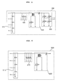
- FIG. 5 is a view showing an example of an internal circuit diagram of a junction box of the photovoltaic module of FIG. 1 .
- the junction box 200 may include a bypass diode unit 510, the capacitor unit 520, the dc/dc converter unit 530, and the inverter unit 540.
- the junction box 200 outputs AC power.
- Such a junction box 200 may be called a micro-inverter.
- the bypass diode unit 510 includes first to third bypass diodes Da, Db, and Dc disposed between a, b, c, and d nodes which correspond to the first to fourth conductive lines 135a, 135b, 135c, and 135d, respectively.
- the capacitor unit 520 stores DC power supplied from the solar cell module 100.
- FIG. 5 it is illustrated that three capacitors Ca, Cb, and Cc are connected in parallel, but the capacitor unit is not limited thereto and the three capacitors may be connected in series or may be connected in series and parallel.
- the capacitor unit 520 is detachably attached to the junction box 200.
- each of the capacitors Ca, Cb, and Cc have a stacked structure in which they are disposed in parallel with each other within a frame.
- the capacitor unit 520 may be detachably mounted as a module in a recess within the junction box 200. According to this structure, when the capacitor unit 520 is to be replaced due to its life span or when the capacitor unit 520 is broken down, the capacitor unit 520 may be easily replaced.
- the dc/dc converter unit 530 performs conversion of DC power level by using the DC power stored in the capacitor unit 520.
- a flyback converter using a turn-on timing of a switching element S1 and a winding ratio of a transformer T is illustrated. Accordingly, voltage boosting of a dc level may be performed.
- a boost converter, a buck converter, a forward converter, or the like may also be used as the dc/dc converter unit 530, or a combination thereof (e.g., a cascaded buck-boost converter, or the like) may also be used as the dc/dc converter unit 530.
- the inverter unit 540 converts the level-converted DC power into AC power.
- a full-bridge inverter is illustrated. Namely, upper arm switching elements Sa and Sb connected in series and lower arm switching elements S'a and S'b connected in series are paired, and a total of two pairs of upper and lower arm switching elements are connected in parallel (Sa&S'a, Sb&S'b). Diodes are connected reversely parallel to the respective switching elements Sa, S'a, Sb, and S'b.
- the switching elements in the inverter unit 540 are turned on or off based on an inverter switching control signal from an inverter controller (not shown). Accordingly, AC power having a certain frequency is outputted.
- the AC power has the same frequency (about 60Hz) as an AC frequency of grid.
- a capacitor unit (not shown) for storing the level-converted dc power may be further provided between the dc/dc converter unit 530 and the inverter unit 540.
- the capacitor unit (not shown) may include a plurality of capacitors, like the foregoing capacitor unit 520 does.
- the junction box 200 includes the capacitor unit storing DC power, the dc/dc converter unit for converting the level of the stored DC power and outputting the same, and the inverter unit for converting the level-converted DC power into AC power and outputting the same, AC power may be simply supplied through the junction box 200. Also, the installation of the photovoltaic module 50 may be facilitated, and the capacitor may be easily increased in configuring a solar photovoltaic system including a plurality of photovoltaic modules.
- FIG. 6 is a view showing another example of an internal circuit diagram of a junction box of the photovoltaic module of FIG. 1 .
- the junction box 200 may include the bypass diode unit 510, the capacitor unit 520, and the dc/dc converter unit 530. Unlike the internal circuit diagram of FIG. 5 , the internal circuit diagram of FIG. 6 does not include the inverter unit 540.
- the junction box 200 may be able to output DC power.
- a power optimizer when the junction box 200 executes a power optimizing function, such a junction box 200 may be called a power optimizer.
- the junction box 200 includes the capacitor unit storing DC power and the dc/dc converter unit converting the level of the stored DC power and outputting the same, the DC power may be simply supplied through the junction box 200. Also, the installation of the photovoltaic module 50 may be facilitated, and the capacitor may be easily increased in configuring a solar photovoltaic system including a plurality of photovoltaic modules.
- FIG. 7 is a view showing an example of a circuit diagram related to a capacitor unit of FIG. 5 .
- the capacitor unit 520 stores DC power supplied from the solar cell module 100.
- an overcurrent such as peak current is instantly generated.
- the capacitor elements C1, Cb, and Cc within the capacitor unit 520 are highly likely to be damaged.
- an overcurrent preventing unit 515 is disposed between the bypass diode unit 510 and the capacitor unit 520, and a controller 550 may be further provided to control the overcurrent preventing unit 515.
- the junction box 200 may further include an overcurrent preventing unit 515 and a controller 550.
- the overcurrent preventing unit 515 may include a first switching element Sf1 turned on during the initial operation, a second switching element Sf2 turned on after the initial operation, and a resistor element Rf connected in series to the first switching element Sf1.
- a first current detection unit A detects current ic1 flowing to the capacitor unit 520
- a voltage detection unit B detects voltage vc1 stored in the capacitor unit 520.
- the detected current ic1 and the voltage vc1 are inputted to the controller 550.
- the second current detection unit C detects current ic2 supplied to the dc/dc converter unit 530.
- the detected current ic2 is inputted to the controller 550.
- the controller 550 outputs turn-on timing signals Sc1 and Sc2 of the first switching element Sf1 and the second switching element Sf2 based on the detected current ic1 or ic2 or the voltage vc1.
- the controller 550 may turn off the first switching element Sf1 and turn on the second switching element Sf2.
- the controller 550 may turn off both the first switching element S1 and the second switching element Sf2 to prevent supply of DC power supplied from the solar cell module 100 to the capacitor unit 520.
- the controller 550 may output a converter control signal for controlling the switching element of the dc/dc converter unit 530 of FIG. 5 . Also, the controller 550 may output an inverter control signal for controlling the switching elements of the inverter unit 540.
- controller 550 may control the switching element of the dc/dc converter unit 530 of FIG. 5 to perform power optimizing (to be described).
- the overcurrent preventing unit 515 and the controller 550 may applicable to the junction box of FIG. 6 as well as to the junction box of FIG. 5 .
- FIG. 8 is a view showing an example of the configuration of a photovoltaic system.
- the solar photovoltaic system may include a plurality of photovoltaic modules 50a, 50b, ..., 50n.
- the photovoltaic modules 50a, 50b, ..., 50n may include junction boxes 200a, 200b, ..., 200n outputting AC power, respectively.
- the junction boxes 200a, 200b, ..., 200n may be micro-inverters, and AC power output from the respective junction boxes 200a, 200b, ..., 200n is supplied to a grid.
- the internal circuit of the junction box 200 illustrated in FIG. 5 may be applied to the micro-inverter of FIG. 8 .
- FIG. 9 is a view showing another example of the configuration of a solar photovoltaic system according to an embodiment of the present invention.
- the solar photovoltaic system may include a plurality of photovoltaic modules 50a, 50b, ..., 50n.
- the photovoltaic modules 50a, 50b, ..., 50n may include junction boxes 1200a, 1200b, ..., 1200n outputting DC power, respectively.
- an inverter unit 1210 for converting DC power output from the respective photovoltaic modules 50a, 50b, ..., 50n into AC power may be further provided.
- the junction boxes 1200a, 1200b, ..., 1200n may perform power optimizing in order to effectively output DC power.
- the internal circuit of the junction box 200 of FIG. 6 may be applied to the power optimizer of FIG. 9 .
- FIGS. 10A and 10B are schematic diagrams referred to in explaining power optimizing of the solar photovoltaic system according to an embodiment of the present invention.
- each of the solar cell modules in particular, the controller 550 of each of the solar cell modules, may control a voltage output, or the like, of its own upon receiving a current value or a voltage value supplied from a different solar cell module.
- junction box 200 illustrated in FIG. 6 may be applicable to the power optimizing of FIG. 10B .
- the junction box since the junction box includes the capacitor unit storing DC power and the dc/dc converter converting the level of the stored DC power and outputting the same, power may be easily supplied through the junction box.
- the photovoltaic module having such a junction box may be easily installed, and when a solar photovoltaic system including a plurality of photovoltaic modules is configured, the capacity may be easily increased.
- the junction box includes the capacitor unit storing DC power, the dc/dc converter unit converting the level of the stored DC power and outputting the same, and the inverter unit converting the level-converted DC power into AC power and outputting the same, AC power may be simply supplied through the junction box.
- the capacitor unit is detachably mounted, when the capacitor unit is defective, it may be easily replaced.
- the photovoltaic module according to the embodiments of the present disclosure is not limited in its application of the configurations and methods, but the entirety or a portion of the embodiments may be selectively combined to be configured into various modifications.
Abstract
Description
- his application claims the priority benefit of Korean Patent Application No.
10-2011-0033728, filed on April 12, 2011 - The present disclosure relates to a photovoltaic module (or a solar module) and, more particularly, to a photovoltaic module capable of easily supplying power
- Recently, as existing energy resources such as oil or coal are expected to be exhausted, an interest in alternative energy for replacing oil or coal is increasing. In particular, a solar cell which directly converts (or transforms) solar energy into electric energy by using a semiconductor element is getting the spotlight as a next-generation cell.
- Meanwhile, a photovoltaic module refers to a device in which solar cells for photovoltaic power generation are connected in series or in parallel, and the photovoltaic module may include a junction box collecting electricity produced by the solar cells.
- one aspect provides a photovoltaic module capable of easily supply power through a junction box.
- Another aspect provides a photovoltaic module which may be easily installed and is advantageous for increasing capacity in constituting a system.
- According to another aspect, there is provided a photovoltaic module including: a solar cell module including a plurality of solar cells; and a junction box including a capacitor unit attached to one face of the solar cell module and that stores DC power supplied from the solar cell module, and a dc/dc converter unit to convert the level of the stored DC power and output the same.
- The foregoing and other objects, features, aspects and advantages according to the disclosure will become more apparent from the following detailed description when taken in conjunction with the accompanying drawings.
-
-
FIG. 1 is a front view of a photovoltaic module according to an embodiment of the present invention. -
FIG. 2 is a rear view of the photovoltaic module ofFIG. 1 . -
FIG. 3 is an exploded perspective view of the photovoltaic module ofFIG. 1 . -
FIG. 4 is a view showing an example of bypass diodes of the photovoltaic module ofFIG. 1 . -
FIG. 5 is a view showing an example of an internal circuit diagram of a junction box of the photovoltaic module according to an embodiment of the invention. -
FIG. 6 is a view showing another example of an internal circuit diagram of a junction box of the photovoltaic module according to another embodiment of the invention. -
FIG. 7 is a view showing an example of a circuit diagram related to a capacitor unit according to an embodiment of the invention. -
FIG. 8 is a view showing an example of the configuration of a photovoltaic system. -
FIG. 9 is a view showing another example of the configuration of a photovoltaic system. -
FIGS. 10A and10B are schematic diagrams referred to explain power optimizing of the photovoltaic system according to an embodiment of the present invention. - Exemplary embodiments of the present invention will now be described in detail with reference to the accompanying drawings.
- In the following description, usage of suffixes such as `module', `part' or 'unit' used for referring to elements is given merely to facilitate explanation of the present disclosure, without having any significant meaning in itself. Thus, the 'module' and `part' may be interchangeably used.
-
FIG. 1 is a front view of a photovoltaic module according to an embodiment of the present invention.FIG. 2 is a rear view of the photovoltaic module ofFIG. 1 .FIG. 3 is an exploded perspective view of the photovoltaic module ofFIG. 1 . - With reference to
FIGS. 1 to 3 , aphotovoltaic module 50 according to an embodiment of the present invention includes asolar cell module 100 and ajunction box 200 positioned on one surface of thesolar cell module 100. Thesolar cell module 50 may further include a heat releasing member (not shown) disposed between thesolar cell module 100 and thejunction box 200. - The
solar cell module 100 may include a plurality ofsolar cells 130. Also, thesolar cell module 100 may further include afirst sealing member 120 and asecond sealing member 150 positioned on lower and upper surfaces of the plurality ofsolar cells 130, arear substrate 110 positioned on a lower surface of thefirst sealing member 120, and afront substrate 160 positioned on an upper surface of thesecond sealing member 150. - Each of the
solar cells 130 is a semiconductor device converting solar energy into electric energy and may be a silicon solar cell, a compound semiconductor solar cell, a tandem solar cell, a dye-sensitized solar cell, a CdTe or CIGS type solar cell, or the like. - Each of the
solar cells 130 is configured to have a light receiving face to which solar light is made incident and a rear face, which is opposite to the light receiving face. For example, each of thesolar cells 130 may include a silicon substrate having a first conductivity type, a semiconductor layer formed on the silicon substrate and having a second conductivity type which is opposite to the first conductivity type, an anti-reflective film having one or more openings that expose a portion of the second conductivity type semiconductor layer and formed on the second conductivity type semiconductor layer, a front electrode in contact with the portion of the second conductivity type semiconductor layer through the one or more openings, and a rear electrode formed on a rear surface of the silicon substrate. - The respective
solar cells 130 may be electrically connected in series, in parallel, or in series and parallel. In detail, the plurality ofsolar cells 130 may be electrically connected by aribbon 133. Theribbon 133 may be bonded to the front electrode formed on a light receiving face of a solar cell and to the rear electrode formed on a rear surface of an adjacentsolar cell 130. - In the drawing, it is illustrated that the
ribbons 133 are formed in two rows, and thesolar cells 130 are connected in a row by theribbons 133, formingsolar cell strings 140. Accordingly, sixstrings - Meanwhile, the respective solar cell strings may be electrically connected by bus ribbons.
FIG. 1 illustrates that the firstsolar cell string 140a and the secondsolar cell string 140b, the thirdsolar cell string 140c and the fourthsolar cell string 140d, and the fifthsolar string 140e and the sixthsolar cell string 140f are electrically connected bybus ribbons solar cell module 100, respectively. Also,FIG. 1 illustrates that the secondsolar cell string 140b and the thirdsolar cell string 140c, and the fourthsolar cell string 140d and the fifthsolar cell string 140e are electrically connected bybus ribbons solar cell module 100, respectively. - Meanwhile, the ribbon connected to the first string, the bus ribbons 145b and 145d, and the ribbon connected to the sixth string are electrically connected to the first to fourth
conductive lines conductive lines FIG. 4 ) within thejunction box 200 disposed on the rear surface of thesolar cell module 100. In the drawing, it is illustrated that the first to fourthconductive lines solar cell module 100 through openings formed on thesolar cell module 100. - Meanwhile, preferably, the
junction box 200 is disposed to be adjacent to be closer to an end portion, among both end portions of thesolar cell module 100, where the conductive lines extend. - In
FIGS. 1 and2 , the first to fourthconductive lines solar cell module 100 to the rear surface of thesolar cell module 100, so thejunction box 200 is illustrated to be positioned at the upper portion of the rear surface of thesolar cell module 100. Accordingly, the length of the conductive lines may be reduced, and thus, a power lost may be reduced. - Unlike the configuration illustrated in
FIGS. 1 and2 , if the first to fourthconductive lines solar cell module 100 to the rear surface of thesolar cell module 100, thejunction box 200 may be positioned at a lower portion of the rear surface of thesolar cell module 100. - The
rear substrate 110, as a back sheet, performs functions such as waterproofing, insulating, and filtering of ultraviolet rays. Therear substrate 110 may be a TPT (Tedlar/PET/Tedlar) type rear substrate, but is not meant to be limited thereto. Also, inFIG. 3 , therear substrate 110 has a rectangular shape but it may be fabricated to have various shapes such as a circular shape, a semicircular shape, or the like, according to an environment in which thesolar cell module 100 is installed. - Meanwhile, the
first sealing member 120 may have the same size as that of therear substrate 110 and attached to therear substrate 110, and the plurality ofsolar cells 130 may be positioned to adjoin each other in several number of rows on thefirst sealing member 120. - The
second sealing member 150 is positioned on thesolar cells 130 and may be bonded to the first sealingmember 120 through lamination. - Here, the
first sealing member 120 and thesecond sealing member 150 may enable respective elements of the solar cells to be chemically bonded. Thefirst sealing member 120 and thesecond sealing member 150 may be, for example, an ethylene vinyl acetate (EVA) film, or the like. - Meanwhile, preferably, the
front substrate 160 is positioned on thesecond sealing member 150 to allow solar light to be transmitted therethrough, and may be tempered glass in order to protect thesolar cells 130 against external impact, or the like. Also, more preferably, in order to prevent a reflection of solar light and increase transmittance of solar light, the front substrate may be a low iron tempered glass including a small amount of iron. - The
junction box 200 is attached to the rear surface of thesolar cell module 100, and may convert power by using DC power supplied from thesolar cell module 100. In detail, thejunction box 200 may include a capacitor unit (520 inFIG. 5 ) for storing DC power and a dc/dc converter unit (530 inFIG. 5 ) for converting the level of the DC power and outputting the same. Also, thejunction box 200 may further include bypass diodes Da, Db, and Dc (510 inFIG. 5 ) for preventing a back flow of current among solar cell strings. Also, thejunction box 200 may further include an inverter unit (540 inFIG. 5 ) for converting DC power into AC power. This will be described later with reference toFIG. 5 . - In this manner, the
junction box 200 according to an embodiment of the present invention may include at least the bypass diodes Da, Db, and Dc, the capacitor unit for storing DC power, and the dc/dc converter unit. - When the
junction box 200 is integrally formed with thesolar cell module 100, a loss of DC power generated by eachsolar cell module 100 may be minimized and effectively managed, like a solar photovoltaic system ofFIG. 8 or9 . Meanwhile, the integrally formedjunction box 200 may be called an MIC (Module Integrated Converter). - Meanwhile, in order to prevent an infiltration of moisture to circuit elements in the
junction box 200, the interior of the junction box may be coated with silicon, or the like. - Meanwhile, openings (not shown) are formed on the
junction box 200 in order to allow the foregoing first to fourthconductive lines junction box 200. - When the
junction box 200 operates, heat having a high temperature is generated from the bypass diodes Da, Db, and Dc, or the like. The generated heat may reduce the efficiency of particularsolar cells 130 arranged at the position where thejunction box 200 is attached. - Thus, in order to prevent the efficiency problem, the
photovoltaic module 50 according to an embodiment of the present invention may further include a heat releasing member (not shown) disposed between thesolar cell model 100 and thejunction box 200. In order to dissipate heat generated by thejunction box 200, preferably, the heat releasing member may have a larger sectional area than that of a plate (not shown). For example, the heat releasing member may be formed on the entirety of the rear surface of thesolar cell module 100. Preferably, the heat releasing member is made of a metal material such as gold (Au), silver (Ag), copper (Cu), aluminum (Al), tungsten (W), or the like. - An external connection terminal (not shown) may be formed at one side of the
junction box 160 in order to output power-converted DC power or AC power to the outside. -
FIG. 4 is a view showing an example of bypass diodes of the photovoltaic module ofFIG. 1 . - With reference to
FIG. 4 , the bypass diodes Da, Db, Dc may be connected correspondingly according to the sixsolar cell strings solar cell string 140a and thefirst bus ribbon 145b to bypass the firstsolar cell string 140a and the secondsolar cell string 140b when a reverse voltage occurs in the firstsolar cell string 140a or the secondsolar cell string 140b. - For example, when a voltage of about 0.6V, which is generated in a normal solar cell, is generated, the potential of a cathode electrode of the first bypass diode D1 is higher by about 12V (=0.6V*20) than that of an anode electrode of the first bypass diode D1. Namely, the first bypass diode D1 performs a normal operation, rather than a bypassing operation.
- Meanwhile, when a hot spot occurs such as when shade occurs in a solar cell of the first
solar cell string 140a or when a foreign object is attached, a reverse voltage (about 15V), not the voltage of about 0.6V, is generated from the solar cell. Accordingly, the potential of the anode electrode of the first bypass diode Da is higher by about 15V than that of the cathode electrode. Then, the first bypass diode Da performs a bypassing operation. Thus, the voltage generated in the solar cells in the firstsolar cell string 140a and the secondsolar cell string 140b is not supplied to thejunction box 200. In this manner, when a reverse voltage is generated in some of the solar cells, it is bypassed, thus preventing the corresponding solar cells, or the like, from being damaged. Also, generated DC power may be supplied, except for the hot spot area. - The second bypass diode Db is connected between the
first bus ribbon 145b and thesecond bus ribbon 145d, and when a reverse voltage is generated in the thirdsolar cell string 140c or the fourthsolar cell string 140d, the second bypass diode Db bypasses the thirdsolar cell string 140c and the fourthsolar cell string 140d. - The third bypass diode Dc is connected between the sixth solar cell string and the
second bus ribbon 145d, and when a reverse voltage is generated in the fifthsolar cell string 140e or the sixthsolar cell string 140f, the third bypass diode Dc bypasses the fifth solar cell string and the sixth solar cell string. - Meanwhile, unlike the case of
FIG. 4 , six bypass diodes may be connected correspondingly according to six solar cell strings, and various other modifications may also be implemented. -
FIG. 5 is a view showing an example of an internal circuit diagram of a junction box of the photovoltaic module ofFIG. 1 . - With reference to
FIG. 5 , thejunction box 200 according to an embodiment of the present invention may include abypass diode unit 510, thecapacitor unit 520, the dc/dc converter unit 530, and theinverter unit 540. - The
junction box 200 outputs AC power. Such ajunction box 200 may be called a micro-inverter. - The
bypass diode unit 510 includes first to third bypass diodes Da, Db, and Dc disposed between a, b, c, and d nodes which correspond to the first to fourthconductive lines - The
capacitor unit 520 stores DC power supplied from thesolar cell module 100. InFIG. 5 , it is illustrated that three capacitors Ca, Cb, and Cc are connected in parallel, but the capacitor unit is not limited thereto and the three capacitors may be connected in series or may be connected in series and parallel. - According to an embodiment of the present invention, preferably, the
capacitor unit 520 is detachably attached to thejunction box 200. For example, each of the capacitors Ca, Cb, and Cc have a stacked structure in which they are disposed in parallel with each other within a frame. Thecapacitor unit 520 may be detachably mounted as a module in a recess within thejunction box 200. According to this structure, when thecapacitor unit 520 is to be replaced due to its life span or when thecapacitor unit 520 is broken down, thecapacitor unit 520 may be easily replaced. - The dc/
dc converter unit 530 performs conversion of DC power level by using the DC power stored in thecapacitor unit 520. InFIG. 5 , a flyback converter using a turn-on timing of a switching element S1 and a winding ratio of a transformer T is illustrated. Accordingly, voltage boosting of a dc level may be performed. - Besides the flyback converter illustrated in
FIG. 5 , a boost converter, a buck converter, a forward converter, or the like, may also be used as the dc/dc converter unit 530, or a combination thereof (e.g., a cascaded buck-boost converter, or the like) may also be used as the dc/dc converter unit 530. - The
inverter unit 540 converts the level-converted DC power into AC power. InFIG. 5 , a full-bridge inverter is illustrated. Namely, upper arm switching elements Sa and Sb connected in series and lower arm switching elements S'a and S'b connected in series are paired, and a total of two pairs of upper and lower arm switching elements are connected in parallel (Sa&S'a, Sb&S'b). Diodes are connected reversely parallel to the respective switching elements Sa, S'a, Sb, and S'b. - The switching elements in the
inverter unit 540 are turned on or off based on an inverter switching control signal from an inverter controller (not shown). Accordingly, AC power having a certain frequency is outputted. Preferably, the AC power has the same frequency (about 60Hz) as an AC frequency of grid. - Meanwhile, a capacitor unit (not shown) for storing the level-converted dc power may be further provided between the dc/
dc converter unit 530 and theinverter unit 540. The capacitor unit (not shown) may include a plurality of capacitors, like the foregoingcapacitor unit 520 does. - As shown in
FIG. 5 , because thejunction box 200 includes the capacitor unit storing DC power, the dc/dc converter unit for converting the level of the stored DC power and outputting the same, and the inverter unit for converting the level-converted DC power into AC power and outputting the same, AC power may be simply supplied through thejunction box 200. Also, the installation of thephotovoltaic module 50 may be facilitated, and the capacitor may be easily increased in configuring a solar photovoltaic system including a plurality of photovoltaic modules. -
FIG. 6 is a view showing another example of an internal circuit diagram of a junction box of the photovoltaic module ofFIG. 1 . - With reference to
FIG. 6 , thejunction box 200 according to an embodiment of the present invention may include thebypass diode unit 510, thecapacitor unit 520, and the dc/dc converter unit 530. Unlike the internal circuit diagram ofFIG. 5 , the internal circuit diagram ofFIG. 6 does not include theinverter unit 540. - Thus, the
junction box 200 may be able to output DC power. In this case, when thejunction box 200 executes a power optimizing function, such ajunction box 200 may be called a power optimizer. - As shown in
FIG. 6 , since thejunction box 200 includes the capacitor unit storing DC power and the dc/dc converter unit converting the level of the stored DC power and outputting the same, the DC power may be simply supplied through thejunction box 200. Also, the installation of thephotovoltaic module 50 may be facilitated, and the capacitor may be easily increased in configuring a solar photovoltaic system including a plurality of photovoltaic modules. -
FIG. 7 is a view showing an example of a circuit diagram related to a capacitor unit ofFIG. 5 . - With reference to
FIG. 7 , thecapacitor unit 520 stores DC power supplied from thesolar cell module 100. In particular, in an initial operation, when current flows from thesolar cell module 100 to thecapacitor unit 520, an overcurrent such as peak current is instantly generated. Then, the capacitor elements C1, Cb, and Cc within thecapacitor unit 520 are highly likely to be damaged. - In an embodiment of the present invention, in order to prevent an introduction of an inrush current or an overcurrent, an
overcurrent preventing unit 515 is disposed between thebypass diode unit 510 and thecapacitor unit 520, and acontroller 550 may be further provided to control theovercurrent preventing unit 515. Namely, thejunction box 200 may further include anovercurrent preventing unit 515 and acontroller 550. - The
overcurrent preventing unit 515 may include a first switching element Sf1 turned on during the initial operation, a second switching element Sf2 turned on after the initial operation, and a resistor element Rf connected in series to the first switching element Sf1. - For example, during the first operation, when the first switching element Sf1 is turned on, an input overcurrent component is partially consumed in the resistor element Rf and stored in the
capacitor unit 520. - Next, when the second switching element Sf2 is turned on after the initial operation, the DC power supplied from the
solar cell module 100 is stored in thecapacitor unit 520. - Meanwhile, a first current detection unit A detects current ic1 flowing to the
capacitor unit 520, and a voltage detection unit B detects voltage vc1 stored in thecapacitor unit 520. The detected current ic1 and the voltage vc1 are inputted to thecontroller 550. - Also, the second current detection unit C detects current ic2 supplied to the dc/
dc converter unit 530. The detected current ic2 is inputted to thecontroller 550. - The
controller 550 outputs turn-on timing signals Sc1 and Sc2 of the first switching element Sf1 and the second switching element Sf2 based on the detected current ic1 or ic2 or the voltage vc1. - For example, when the detected current ic1 or ic2 or the voltage vc1 is higher than a pre-set value, the
controller 550 may turn off the first switching element Sf1 and turn on the second switching element Sf2. - Meanwhile, when the detected current ic1 or ic2 or the voltage vc1 is higher than an allowable value, the
controller 550 may turn off both the first switching element S1 and the second switching element Sf2 to prevent supply of DC power supplied from thesolar cell module 100 to thecapacitor unit 520. - Meanwhile, the
controller 550 may output a converter control signal for controlling the switching element of the dc/dc converter unit 530 ofFIG. 5 . Also, thecontroller 550 may output an inverter control signal for controlling the switching elements of theinverter unit 540. - Meanwhile, the
controller 550 may control the switching element of the dc/dc converter unit 530 ofFIG. 5 to perform power optimizing (to be described). - Meanwhile, the
overcurrent preventing unit 515 and thecontroller 550 may applicable to the junction box ofFIG. 6 as well as to the junction box ofFIG. 5 . -
FIG. 8 is a view showing an example of the configuration of a photovoltaic system. - With reference to
FIG. 8 , the solar photovoltaic system according to an embodiment of the present invention may include a plurality ofphotovoltaic modules photovoltaic modules junction boxes junction boxes respective junction boxes - Meanwhile, the internal circuit of the
junction box 200 illustrated inFIG. 5 according to an embodiment of the present invention may be applied to the micro-inverter ofFIG. 8 . -
FIG. 9 is a view showing another example of the configuration of a solar photovoltaic system according to an embodiment of the present invention. - With reference to
FIG. 9 , the solar photovoltaic system according to an embodiment of the present invention may include a plurality ofphotovoltaic modules photovoltaic modules junction boxes inverter unit 1210 for converting DC power output from the respectivephotovoltaic modules junction boxes - Meanwhile, the internal circuit of the
junction box 200 ofFIG. 6 according to an embodiment of the present invention may be applied to the power optimizer ofFIG. 9 . -
FIGS. 10A and10B are schematic diagrams referred to in explaining power optimizing of the solar photovoltaic system according to an embodiment of the present invention. - First, a case in which power optimizing is not employed will now be described with reference to
FIG. 10A . As illustrated, in a state in which a plurality of solar cell modules are connected in series, when a hot spot occurs insolar cell modules 1320 so that a power loss is made (e.g., 70W power supply), a power loss is also made even in a normal solar cell module 1310 (e.g., 70W power supply). Thus, only power totaling 980 W is supplied. - Next, a case in which power optimizing is employed will now be described with reference to
FIG. 10B . When a hot spot occurs insolar cell modules 1320 so that a power loss is made (e.g., 70W power supply), voltage output from the correspondingsolar cell modules 1320 is lowered so that current supplied from the correspondingsolar cell modules 1320 may be equal to the current supplied from a differentsolar cell module 1310. Thus, although a power loss (e.g., 70W power supply) is made in thesolar cell modules 1320 in which a hot spot occurs, there is no power loss in the normal solar cell module 1310 (e.g., 100W power supply). Thus, power totaling 1340 W may be supplied. - Through power optimizing, the voltage supplied from a solar cell module in which a hot spot occurs may be adjusted according to the current supplied from a different solar cell module. To this end, each of the solar cell modules, in particular, the
controller 550 of each of the solar cell modules, may control a voltage output, or the like, of its own upon receiving a current value or a voltage value supplied from a different solar cell module. - Meanwhile, the
junction box 200 illustrated inFIG. 6 according to an embodiment of the present invention may be applicable to the power optimizing ofFIG. 10B . - According to embodiments of the present invention, since the junction box includes the capacitor unit storing DC power and the dc/dc converter converting the level of the stored DC power and outputting the same, power may be easily supplied through the junction box.
- Also, the photovoltaic module having such a junction box may be easily installed, and when a solar photovoltaic system including a plurality of photovoltaic modules is configured, the capacity may be easily increased.
- Meanwhile, since the junction box includes the capacitor unit storing DC power, the dc/dc converter unit converting the level of the stored DC power and outputting the same, and the inverter unit converting the level-converted DC power into AC power and outputting the same, AC power may be simply supplied through the junction box.
- Also, since the capacitor unit is detachably mounted, when the capacitor unit is defective, it may be easily replaced.
- The photovoltaic module according to the embodiments of the present disclosure is not limited in its application of the configurations and methods, but the entirety or a portion of the embodiments may be selectively combined to be configured into various modifications.
- As the present invention may be embodied in several forms without departing from the characteristics thereof, it should also be understood that the above-described embodiments are not limited by any of the details of the foregoing description, unless otherwise specified, but rather should be construed broadly within its scope as defined in the appended claims, and therefore all changes and modifications that fall within the metes and bounds of the claims, or equivalents of such metes and bounds are therefore intended to be embraced by the appended claims.
Claims (14)
- A photovoltaic module (50) comprising:a solar cell module (100) including a plurality of solar cells; anda junction box (200) including a capacitor unit (520) attached to one face of the solar cell module (100) and that stores DC power supplied from the solar cell module (100), and a dc/dc converter unit (530) to convert the level of the stored DC power and output the same.
- The photovoltaic module of claim 1, wherein the junction box further comprises:a bypass diode (510) to bypass a solar cell in which a reverse voltage occurs among the plurality of solar cells.
- The photovoltaic module of claim 1, wherein the junction box further comprises:an inverter unit (540) to convert the level-converted DC power into AC power and output the same.
- The photovoltaic module of claim 1, further comprising:An overcurrent preventing unit (515) to limit a current based on a DC current supplied from the solar cell module.
- The photovoltaic module of claim 1, wherein the dc/dc converter (530) comprises at least one of a flyback converter, a boost converter, a buck converter, or a forward converter.
- The photovoltaic module of claim 1, wherein the junction box further comprises:A first current detection unit (A) to detect a current supplied to the capacitor unit.
- The photovoltaic module of claim 1, wherein the junction box (200) further comprises:a second current detection unit (C) to detect a current supplied to the dc/dc converter unit.
- The photovoltaic module of claim 1, wherein the junction box (200) further comprises:a voltage detection unit (B) to detect a voltage at both ends of the capacitor unit.
- The photovoltaic module of claim 1, wherein the junction box (200) further comprises:a controller (550) to provide control to stop supplying of the DC power when a voltage at both ends of the capacitor unit is higher than an allowable value.
- The photovoltaic module of claim 1, wherein the capacitor unit (520) is detachably attached to the junction box (200).
- The photovoltaic module of claim 1, wherein the solar cell module (100) further comprises:first and second sealing members (120,150) formed on upper and lower surfaces of the plurality of solar cells (130), respectively;a rear substrate (110) formed on a lower surface of the first sealing member (120); anda front substrate (160) formed on an upper surface of the second sealing member (150).
- The photovoltaic module of claim 1, wherein the solar cell module (100) further comprises a solar cell string (140) formed with some of the plurality of solar cells connected in a row, and a conductive line (135a, 135d) electrically connecting the solar cell string (140) and the junction box (200).
- The photovoltaic module of claim 12, wherein the solar cell module further comprises:a bus ribbon (145a,145b,145c,145d,145e) connected to at least two solar cell strings; andanother conductive line (135b,135c) electrically connecting the bus ribbon and the junction box (200).
- The photovoltaic module of claim 13, wherein the junction box (200) is disposed to be closer to an end portion, to which the conductive line extends, among both end portions of the solar cell module (100).
Applications Claiming Priority (1)
| Application Number | Priority Date | Filing Date | Title |
|---|---|---|---|
| KR1020110033728A KR101796045B1 (en) | 2011-04-12 | 2011-04-12 | Photovoltaic module |
Publications (2)
| Publication Number | Publication Date |
|---|---|
| EP2511959A1 true EP2511959A1 (en) | 2012-10-17 |
| EP2511959B1 EP2511959B1 (en) | 2015-11-18 |
Family
ID=46025300
Family Applications (1)
| Application Number | Title | Priority Date | Filing Date |
|---|---|---|---|
| EP12002331.2A Not-in-force EP2511959B1 (en) | 2011-04-12 | 2012-03-30 | Photovoltaic module |
Country Status (3)
| Country | Link |
|---|---|
| US (2) | US9397609B2 (en) |
| EP (1) | EP2511959B1 (en) |
| KR (1) | KR101796045B1 (en) |
Cited By (4)
| Publication number | Priority date | Publication date | Assignee | Title |
|---|---|---|---|---|
| CN108033250A (en) * | 2017-11-27 | 2018-05-15 | 苏州索力旺新能源科技有限公司 | A kind of photovoltaic junction box transmission detection device |
| US10003194B2 (en) | 2014-10-24 | 2018-06-19 | Enphase Energy, Inc. | Parallel battery system |
| US10749060B2 (en) | 2013-07-05 | 2020-08-18 | Rec Solar Pte. Ltd. | Solar cell assembly |
| WO2020181342A1 (en) * | 2019-03-14 | 2020-09-17 | Maré Brasil Energia E Equipamentos Ltda | Optimized junction box |
Families Citing this family (17)
| Publication number | Priority date | Publication date | Assignee | Title |
|---|---|---|---|---|
| US9755099B2 (en) | 2013-08-14 | 2017-09-05 | Globalfoundries Inc. | Integrated micro-inverter and thin film solar module and manufacturing process |
| GB2522408A (en) | 2014-01-14 | 2015-07-29 | Ibm | Monolithically integrated thin-film device with a solar cell, an integrated battery and a controller |
| US9735699B2 (en) | 2014-01-15 | 2017-08-15 | Lg Electronics Inc. | Integral inverter and solar cell module including the same |
| KR102205161B1 (en) * | 2014-01-15 | 2021-01-19 | 엘지전자 주식회사 | Power converting apparatus, and photovoltaic module |
| US9602048B2 (en) * | 2014-01-15 | 2017-03-21 | Lg Electronics Inc. | Photovoltaic module |
| KR102317140B1 (en) * | 2014-02-19 | 2021-10-22 | 엘지전자 주식회사 | Power converting apparatus, and photovoltaic module |
| US20190036484A1 (en) * | 2015-08-10 | 2019-01-31 | Patton Engineering, Inc. | Efficient Back Supported Solar Panel Systems and Methods |
| KR102000062B1 (en) * | 2016-03-15 | 2019-10-01 | 엘지전자 주식회사 | Photovoltaic module |
| US20170279402A1 (en) * | 2016-03-25 | 2017-09-28 | X Development Llc | Photovoltaic macro-module for solar power generation |
| KR20170124257A (en) * | 2016-05-02 | 2017-11-10 | 엘지전자 주식회사 | Photovoltaic module, and photovoltaic system including the same |
| KR101898587B1 (en) * | 2016-05-04 | 2018-09-13 | 엘지전자 주식회사 | Photovoltaic module and photovoltaic system including the same |
| US20170373635A1 (en) * | 2016-06-24 | 2017-12-28 | Sunpower Corporation | Photovoltaic systems comprising docking assemblies |
| KR101695381B1 (en) * | 2016-07-14 | 2017-01-11 | 에스제이주식회사 | Apparatus for Photovoltaic Junction Box |
| FR3085540B1 (en) * | 2018-08-31 | 2020-09-25 | St Microelectronics Rousset | INTEGRATED DEVICE FOR TEMPORAL MEASUREMENT WITH ULTRA LONG TIME CONSTANT AND MANUFACTURING PROCESS |
| WO2022082769A1 (en) * | 2020-10-23 | 2022-04-28 | 华为数字能源技术有限公司 | Backward flowing slow-start circuit of string photovoltaic inverter |
| KR102553810B1 (en) * | 2021-12-17 | 2023-07-10 | 한국생산기술연구원 | Regenerative load Tester of Distributed Power Architecture for Power Supply Load Test |
| JP2024039854A (en) * | 2022-09-12 | 2024-03-25 | シャープ株式会社 | solar module |
Citations (3)
| Publication number | Priority date | Publication date | Assignee | Title |
|---|---|---|---|---|
| WO2009143253A2 (en) * | 2008-05-20 | 2009-11-26 | Greenray, Inc. | An ac photovoltaic module and inverter assembly |
| US20100206378A1 (en) * | 2009-02-13 | 2010-08-19 | Miasole | Thin-film photovoltaic power system with integrated low-profile high-efficiency inverter |
| WO2010132369A1 (en) * | 2009-05-11 | 2010-11-18 | The Regents Of The University Of Colorado, A Body Corporate | Integrated photovoltaic module |
Family Cites Families (20)
| Publication number | Priority date | Publication date | Assignee | Title |
|---|---|---|---|---|
| JP2001044465A (en) * | 1999-07-28 | 2001-02-16 | Tokico Ltd | Power supply device and power supply system of solar battery |
| US7586770B2 (en) * | 2006-02-24 | 2009-09-08 | Mitsubishi Electric Corporation | Interconnection inverter device |
| JP2007294866A (en) * | 2006-03-31 | 2007-11-08 | Sanyo Electric Co Ltd | Photovoltaic module |
| US20080144294A1 (en) * | 2006-12-06 | 2008-06-19 | Meir Adest | Removal component cartridge for increasing reliability in power harvesting systems |
| FR2912848B1 (en) * | 2007-02-20 | 2010-09-17 | Commissariat Energie Atomique | VOLTAGE LIMITER AND PROTECTION OF A PHOTOVOLTAIC MODULE |
| ES2432380T5 (en) | 2008-03-11 | 2023-03-01 | Cnbm Bengbu Design & Res Institute For Glass Industry Co Ltd | solar module |
| DE102008028462A1 (en) | 2008-06-14 | 2009-12-17 | Kostal Industrie Elektrik Gmbh | Electrical connection and connection box for a solar cell module |
| US20100043868A1 (en) * | 2008-08-06 | 2010-02-25 | David Sun | System and method for integrated solar power generator |
| DE102008050543A1 (en) * | 2008-10-06 | 2010-04-15 | Siemens Aktiengesellschaft | Protection circuit for a DC link of an inverter, in particular a solar inverter, against overvoltages |
| US8435056B2 (en) * | 2009-04-16 | 2013-05-07 | Enphase Energy, Inc. | Apparatus for coupling power generated by a photovoltaic module to an output |
| JP2012527786A (en) * | 2009-05-25 | 2012-11-08 | デイ4 エネルギー インコーポレイテッド | Photovoltaic module string device and protection from shadows therefor |
| KR20100136091A (en) | 2009-06-18 | 2010-12-28 | 다담마이크로 주식회사 | Junction box of solar photovoltaic |
| TW201124684A (en) * | 2010-01-14 | 2011-07-16 | Axuntek Solar Energy | Solar panel heat-dissipating device and related solar panel module |
| US8194375B2 (en) * | 2010-01-19 | 2012-06-05 | General Electric Company | Open circuit voltage protection system and method |
| KR100990116B1 (en) * | 2010-05-17 | 2010-10-29 | 엘지전자 주식회사 | Solar cell module |
| US8837097B2 (en) * | 2010-06-07 | 2014-09-16 | Eaton Corporation | Protection, monitoring or indication apparatus for a direct current electrical generating apparatus or a plurality of strings |
| GB2482653B (en) * | 2010-06-07 | 2012-08-29 | Enecsys Ltd | Solar photovoltaic systems |
| US8395919B2 (en) * | 2010-07-29 | 2013-03-12 | General Electric Company | Photovoltaic inverter system and method of starting same at high open-circuit voltage |
| US20120033392A1 (en) * | 2010-08-09 | 2012-02-09 | Tyco Electronics Corporation | Modular Junction Box for a Photovoltaic Module |
| US8953350B2 (en) * | 2011-04-08 | 2015-02-10 | Sunedison, Inc. | Photovoltaic power converters |
-
2011
- 2011-04-12 KR KR1020110033728A patent/KR101796045B1/en active IP Right Grant
-
2012
- 2012-03-22 US US13/427,139 patent/US9397609B2/en not_active Expired - Fee Related
- 2012-03-30 EP EP12002331.2A patent/EP2511959B1/en not_active Not-in-force
-
2016
- 2016-06-16 US US15/184,143 patent/US10270387B2/en active Active
Patent Citations (3)
| Publication number | Priority date | Publication date | Assignee | Title |
|---|---|---|---|---|
| WO2009143253A2 (en) * | 2008-05-20 | 2009-11-26 | Greenray, Inc. | An ac photovoltaic module and inverter assembly |
| US20100206378A1 (en) * | 2009-02-13 | 2010-08-19 | Miasole | Thin-film photovoltaic power system with integrated low-profile high-efficiency inverter |
| WO2010132369A1 (en) * | 2009-05-11 | 2010-11-18 | The Regents Of The University Of Colorado, A Body Corporate | Integrated photovoltaic module |
Cited By (6)
| Publication number | Priority date | Publication date | Assignee | Title |
|---|---|---|---|---|
| US10749060B2 (en) | 2013-07-05 | 2020-08-18 | Rec Solar Pte. Ltd. | Solar cell assembly |
| EP3017520B1 (en) * | 2013-07-05 | 2020-10-14 | REC Solar Pte. Ltd. | Solar cell assembly |
| US10003194B2 (en) | 2014-10-24 | 2018-06-19 | Enphase Energy, Inc. | Parallel battery system |
| CN108033250A (en) * | 2017-11-27 | 2018-05-15 | 苏州索力旺新能源科技有限公司 | A kind of photovoltaic junction box transmission detection device |
| CN108033250B (en) * | 2017-11-27 | 2024-01-12 | 苏州索力旺新能源科技有限公司 | Conveying detection device for photovoltaic junction box |
| WO2020181342A1 (en) * | 2019-03-14 | 2020-09-17 | Maré Brasil Energia E Equipamentos Ltda | Optimized junction box |
Also Published As
| Publication number | Publication date |
|---|---|
| KR20120116152A (en) | 2012-10-22 |
| US20120262948A1 (en) | 2012-10-18 |
| US10270387B2 (en) | 2019-04-23 |
| US20160301360A1 (en) | 2016-10-13 |
| US9397609B2 (en) | 2016-07-19 |
| EP2511959B1 (en) | 2015-11-18 |
| KR101796045B1 (en) | 2017-11-10 |
Similar Documents
| Publication | Publication Date | Title |
|---|---|---|
| US10270387B2 (en) | Photovoltaic module | |
| US9577573B2 (en) | Photovoltaic module | |
| US10277165B2 (en) | Photovoltaic module | |
| EP2621075B1 (en) | Power converting apparatus and photovoltaic module | |
| US9397610B2 (en) | Photovoltaic module and control method thereof | |
| KR101898587B1 (en) | Photovoltaic module and photovoltaic system including the same | |
| JP6612281B2 (en) | Solar module | |
| KR20120140023A (en) | Photovoltaic module | |
| KR101954194B1 (en) | Power converting apparatus, and photovoltaic module | |
| KR101824983B1 (en) | Photovoltaic module, photovoltaic system and method for controlling the same | |
| KR20130011689A (en) | Photovoltaic module | |
| KR101788013B1 (en) | Photovoltaic module | |
| KR101249899B1 (en) | Photovoltaic module | |
| KR101893816B1 (en) | Photovoltaic module | |
| KR101959302B1 (en) | Photovoltaic module, and photovoltaic system | |
| KR101954195B1 (en) | Power converting apparatus, and photovoltaic module | |
| KR20120134810A (en) | Photovoltaic module | |
| KR20130137926A (en) | Photovoltaic module | |
| KR20120129112A (en) | Combined photovoltaic and photovoltaic thermal system | |
| KR20130019987A (en) | Combined photovoltaic and photovoltaic thermal module |
Legal Events
| Date | Code | Title | Description |
|---|---|---|---|
| PUAI | Public reference made under article 153(3) epc to a published international application that has entered the european phase |
Free format text: ORIGINAL CODE: 0009012 |
|
| 17P | Request for examination filed |
Effective date: 20120330 |
|
| AK | Designated contracting states |
Kind code of ref document: A1 Designated state(s): AL AT BE BG CH CY CZ DE DK EE ES FI FR GB GR HR HU IE IS IT LI LT LU LV MC MK MT NL NO PL PT RO RS SE SI SK SM TR |
|
| AX | Request for extension of the european patent |
Extension state: BA ME |
|
| 17Q | First examination report despatched |
Effective date: 20130409 |
|
| REG | Reference to a national code |
Ref country code: DE Ref legal event code: R079 Ref document number: 602012012273 Country of ref document: DE Free format text: PREVIOUS MAIN CLASS: H01L0031042000 Ipc: H02S0040340000 |
|
| GRAP | Despatch of communication of intention to grant a patent |
Free format text: ORIGINAL CODE: EPIDOSNIGR1 |
|
| RIC1 | Information provided on ipc code assigned before grant |
Ipc: H02S 40/32 20140101ALI20150519BHEP Ipc: H02S 40/34 20140101AFI20150519BHEP |
|
| INTG | Intention to grant announced |
Effective date: 20150616 |
|
| GRAS | Grant fee paid |
Free format text: ORIGINAL CODE: EPIDOSNIGR3 |
|
| GRAA | (expected) grant |
Free format text: ORIGINAL CODE: 0009210 |
|
| AK | Designated contracting states |
Kind code of ref document: B1 Designated state(s): AL AT BE BG CH CY CZ DE DK EE ES FI FR GB GR HR HU IE IS IT LI LT LU LV MC MK MT NL NO PL PT RO RS SE SI SK SM TR |
|
| REG | Reference to a national code |
Ref country code: GB Ref legal event code: FG4D |
|
| REG | Reference to a national code |
Ref country code: CH Ref legal event code: EP |
|
| REG | Reference to a national code |
Ref country code: AT Ref legal event code: REF Ref document number: 761990 Country of ref document: AT Kind code of ref document: T Effective date: 20151215 |
|
| REG | Reference to a national code |
Ref country code: IE Ref legal event code: FG4D |
|
| REG | Reference to a national code |
Ref country code: DE Ref legal event code: R096 Ref document number: 602012012273 Country of ref document: DE |
|
| REG | Reference to a national code |
Ref country code: NL Ref legal event code: FP |
|
| REG | Reference to a national code |
Ref country code: LT Ref legal event code: MG4D |
|
| REG | Reference to a national code |
Ref country code: AT Ref legal event code: MK05 Ref document number: 761990 Country of ref document: AT Kind code of ref document: T Effective date: 20151118 |
|
| PG25 | Lapsed in a contracting state [announced via postgrant information from national office to epo] |
Ref country code: LT Free format text: LAPSE BECAUSE OF FAILURE TO SUBMIT A TRANSLATION OF THE DESCRIPTION OR TO PAY THE FEE WITHIN THE PRESCRIBED TIME-LIMIT Effective date: 20151118 Ref country code: ES Free format text: LAPSE BECAUSE OF FAILURE TO SUBMIT A TRANSLATION OF THE DESCRIPTION OR TO PAY THE FEE WITHIN THE PRESCRIBED TIME-LIMIT Effective date: 20151118 Ref country code: NO Free format text: LAPSE BECAUSE OF FAILURE TO SUBMIT A TRANSLATION OF THE DESCRIPTION OR TO PAY THE FEE WITHIN THE PRESCRIBED TIME-LIMIT Effective date: 20160218 Ref country code: HR Free format text: LAPSE BECAUSE OF FAILURE TO SUBMIT A TRANSLATION OF THE DESCRIPTION OR TO PAY THE FEE WITHIN THE PRESCRIBED TIME-LIMIT Effective date: 20151118 Ref country code: IS Free format text: LAPSE BECAUSE OF FAILURE TO SUBMIT A TRANSLATION OF THE DESCRIPTION OR TO PAY THE FEE WITHIN THE PRESCRIBED TIME-LIMIT Effective date: 20160318 |
|
| PG25 | Lapsed in a contracting state [announced via postgrant information from national office to epo] |
Ref country code: LV Free format text: LAPSE BECAUSE OF FAILURE TO SUBMIT A TRANSLATION OF THE DESCRIPTION OR TO PAY THE FEE WITHIN THE PRESCRIBED TIME-LIMIT Effective date: 20151118 Ref country code: SE Free format text: LAPSE BECAUSE OF FAILURE TO SUBMIT A TRANSLATION OF THE DESCRIPTION OR TO PAY THE FEE WITHIN THE PRESCRIBED TIME-LIMIT Effective date: 20151118 Ref country code: PT Free format text: LAPSE BECAUSE OF FAILURE TO SUBMIT A TRANSLATION OF THE DESCRIPTION OR TO PAY THE FEE WITHIN THE PRESCRIBED TIME-LIMIT Effective date: 20160318 Ref country code: PL Free format text: LAPSE BECAUSE OF FAILURE TO SUBMIT A TRANSLATION OF THE DESCRIPTION OR TO PAY THE FEE WITHIN THE PRESCRIBED TIME-LIMIT Effective date: 20151118 Ref country code: RS Free format text: LAPSE BECAUSE OF FAILURE TO SUBMIT A TRANSLATION OF THE DESCRIPTION OR TO PAY THE FEE WITHIN THE PRESCRIBED TIME-LIMIT Effective date: 20151118 Ref country code: FI Free format text: LAPSE BECAUSE OF FAILURE TO SUBMIT A TRANSLATION OF THE DESCRIPTION OR TO PAY THE FEE WITHIN THE PRESCRIBED TIME-LIMIT Effective date: 20151118 Ref country code: GR Free format text: LAPSE BECAUSE OF FAILURE TO SUBMIT A TRANSLATION OF THE DESCRIPTION OR TO PAY THE FEE WITHIN THE PRESCRIBED TIME-LIMIT Effective date: 20160219 Ref country code: AT Free format text: LAPSE BECAUSE OF FAILURE TO SUBMIT A TRANSLATION OF THE DESCRIPTION OR TO PAY THE FEE WITHIN THE PRESCRIBED TIME-LIMIT Effective date: 20151118 |
|
| PG25 | Lapsed in a contracting state [announced via postgrant information from national office to epo] |
Ref country code: CZ Free format text: LAPSE BECAUSE OF FAILURE TO SUBMIT A TRANSLATION OF THE DESCRIPTION OR TO PAY THE FEE WITHIN THE PRESCRIBED TIME-LIMIT Effective date: 20151118 |
|
| REG | Reference to a national code |
Ref country code: DE Ref legal event code: R097 Ref document number: 602012012273 Country of ref document: DE |
|
| PG25 | Lapsed in a contracting state [announced via postgrant information from national office to epo] |
Ref country code: EE Free format text: LAPSE BECAUSE OF FAILURE TO SUBMIT A TRANSLATION OF THE DESCRIPTION OR TO PAY THE FEE WITHIN THE PRESCRIBED TIME-LIMIT Effective date: 20151118 Ref country code: BE Free format text: LAPSE BECAUSE OF NON-PAYMENT OF DUE FEES Effective date: 20160331 Ref country code: SM Free format text: LAPSE BECAUSE OF FAILURE TO SUBMIT A TRANSLATION OF THE DESCRIPTION OR TO PAY THE FEE WITHIN THE PRESCRIBED TIME-LIMIT Effective date: 20151118 Ref country code: RO Free format text: LAPSE BECAUSE OF FAILURE TO SUBMIT A TRANSLATION OF THE DESCRIPTION OR TO PAY THE FEE WITHIN THE PRESCRIBED TIME-LIMIT Effective date: 20151118 Ref country code: DK Free format text: LAPSE BECAUSE OF FAILURE TO SUBMIT A TRANSLATION OF THE DESCRIPTION OR TO PAY THE FEE WITHIN THE PRESCRIBED TIME-LIMIT Effective date: 20151118 Ref country code: SK Free format text: LAPSE BECAUSE OF FAILURE TO SUBMIT A TRANSLATION OF THE DESCRIPTION OR TO PAY THE FEE WITHIN THE PRESCRIBED TIME-LIMIT Effective date: 20151118 |
|
| PLBE | No opposition filed within time limit |
Free format text: ORIGINAL CODE: 0009261 |
|
| STAA | Information on the status of an ep patent application or granted ep patent |
Free format text: STATUS: NO OPPOSITION FILED WITHIN TIME LIMIT |
|
| 26N | No opposition filed |
Effective date: 20160819 |
|
| PG25 | Lapsed in a contracting state [announced via postgrant information from national office to epo] |
Ref country code: LU Free format text: LAPSE BECAUSE OF FAILURE TO SUBMIT A TRANSLATION OF THE DESCRIPTION OR TO PAY THE FEE WITHIN THE PRESCRIBED TIME-LIMIT Effective date: 20160330 Ref country code: MC Free format text: LAPSE BECAUSE OF FAILURE TO SUBMIT A TRANSLATION OF THE DESCRIPTION OR TO PAY THE FEE WITHIN THE PRESCRIBED TIME-LIMIT Effective date: 20151118 |
|
| REG | Reference to a national code |
Ref country code: CH Ref legal event code: PL |
|
| GBPC | Gb: european patent ceased through non-payment of renewal fee |
Effective date: 20160330 |
|
| PG25 | Lapsed in a contracting state [announced via postgrant information from national office to epo] |
Ref country code: SI Free format text: LAPSE BECAUSE OF FAILURE TO SUBMIT A TRANSLATION OF THE DESCRIPTION OR TO PAY THE FEE WITHIN THE PRESCRIBED TIME-LIMIT Effective date: 20151118 |
|
| REG | Reference to a national code |
Ref country code: IE Ref legal event code: MM4A |
|
| PG25 | Lapsed in a contracting state [announced via postgrant information from national office to epo] |
Ref country code: BE Free format text: LAPSE BECAUSE OF FAILURE TO SUBMIT A TRANSLATION OF THE DESCRIPTION OR TO PAY THE FEE WITHIN THE PRESCRIBED TIME-LIMIT Effective date: 20151118 |
|
| REG | Reference to a national code |
Ref country code: FR Ref legal event code: ST Effective date: 20161130 |
|
| PG25 | Lapsed in a contracting state [announced via postgrant information from national office to epo] |
Ref country code: GB Free format text: LAPSE BECAUSE OF NON-PAYMENT OF DUE FEES Effective date: 20160330 Ref country code: LI Free format text: LAPSE BECAUSE OF NON-PAYMENT OF DUE FEES Effective date: 20160331 Ref country code: IE Free format text: LAPSE BECAUSE OF NON-PAYMENT OF DUE FEES Effective date: 20160330 Ref country code: CH Free format text: LAPSE BECAUSE OF NON-PAYMENT OF DUE FEES Effective date: 20160331 Ref country code: FR Free format text: LAPSE BECAUSE OF NON-PAYMENT OF DUE FEES Effective date: 20160331 |
|
| PG25 | Lapsed in a contracting state [announced via postgrant information from national office to epo] |
Ref country code: MT Free format text: LAPSE BECAUSE OF FAILURE TO SUBMIT A TRANSLATION OF THE DESCRIPTION OR TO PAY THE FEE WITHIN THE PRESCRIBED TIME-LIMIT Effective date: 20151118 |
|
| PGFP | Annual fee paid to national office [announced via postgrant information from national office to epo] |
Ref country code: NL Payment date: 20180207 Year of fee payment: 7 |
|
| PG25 | Lapsed in a contracting state [announced via postgrant information from national office to epo] |
Ref country code: CY Free format text: LAPSE BECAUSE OF FAILURE TO SUBMIT A TRANSLATION OF THE DESCRIPTION OR TO PAY THE FEE WITHIN THE PRESCRIBED TIME-LIMIT Effective date: 20151118 Ref country code: HU Free format text: LAPSE BECAUSE OF FAILURE TO SUBMIT A TRANSLATION OF THE DESCRIPTION OR TO PAY THE FEE WITHIN THE PRESCRIBED TIME-LIMIT; INVALID AB INITIO Effective date: 20120330 |
|
| PGFP | Annual fee paid to national office [announced via postgrant information from national office to epo] |
Ref country code: IT Payment date: 20180313 Year of fee payment: 7 |
|
| PG25 | Lapsed in a contracting state [announced via postgrant information from national office to epo] |
Ref country code: TR Free format text: LAPSE BECAUSE OF FAILURE TO SUBMIT A TRANSLATION OF THE DESCRIPTION OR TO PAY THE FEE WITHIN THE PRESCRIBED TIME-LIMIT Effective date: 20151118 Ref country code: MK Free format text: LAPSE BECAUSE OF FAILURE TO SUBMIT A TRANSLATION OF THE DESCRIPTION OR TO PAY THE FEE WITHIN THE PRESCRIBED TIME-LIMIT Effective date: 20151118 Ref country code: MT Free format text: LAPSE BECAUSE OF FAILURE TO SUBMIT A TRANSLATION OF THE DESCRIPTION OR TO PAY THE FEE WITHIN THE PRESCRIBED TIME-LIMIT Effective date: 20160331 |
|
| PG25 | Lapsed in a contracting state [announced via postgrant information from national office to epo] |
Ref country code: BG Free format text: LAPSE BECAUSE OF FAILURE TO SUBMIT A TRANSLATION OF THE DESCRIPTION OR TO PAY THE FEE WITHIN THE PRESCRIBED TIME-LIMIT Effective date: 20151118 |
|
| PG25 | Lapsed in a contracting state [announced via postgrant information from national office to epo] |
Ref country code: AL Free format text: LAPSE BECAUSE OF FAILURE TO SUBMIT A TRANSLATION OF THE DESCRIPTION OR TO PAY THE FEE WITHIN THE PRESCRIBED TIME-LIMIT Effective date: 20151118 |
|
| PGFP | Annual fee paid to national office [announced via postgrant information from national office to epo] |
Ref country code: DE Payment date: 20190207 Year of fee payment: 8 |
|
| REG | Reference to a national code |
Ref country code: NL Ref legal event code: MM Effective date: 20190401 |
|
| PG25 | Lapsed in a contracting state [announced via postgrant information from national office to epo] |
Ref country code: NL Free format text: LAPSE BECAUSE OF NON-PAYMENT OF DUE FEES Effective date: 20190401 |
|
| PG25 | Lapsed in a contracting state [announced via postgrant information from national office to epo] |
Ref country code: IT Free format text: LAPSE BECAUSE OF NON-PAYMENT OF DUE FEES Effective date: 20190330 |
|
| REG | Reference to a national code |
Ref country code: DE Ref legal event code: R119 Ref document number: 602012012273 Country of ref document: DE |
|
| PG25 | Lapsed in a contracting state [announced via postgrant information from national office to epo] |
Ref country code: DE Free format text: LAPSE BECAUSE OF NON-PAYMENT OF DUE FEES Effective date: 20201001 |